WO2012160909A1 - 直流昇圧装置及びこれを用いた太陽光発電システム - Google Patents
直流昇圧装置及びこれを用いた太陽光発電システム Download PDFInfo
- Publication number
- WO2012160909A1 WO2012160909A1 PCT/JP2012/060365 JP2012060365W WO2012160909A1 WO 2012160909 A1 WO2012160909 A1 WO 2012160909A1 JP 2012060365 W JP2012060365 W JP 2012060365W WO 2012160909 A1 WO2012160909 A1 WO 2012160909A1
- Authority
- WO
- WIPO (PCT)
- Prior art keywords
- capacitor
- booster
- power
- converter
- output
- Prior art date
- Legal status (The legal status is an assumption and is not a legal conclusion. Google has not performed a legal analysis and makes no representation as to the accuracy of the status listed.)
- Ceased
Links
Images





Classifications
-
- H—ELECTRICITY
- H02—GENERATION; CONVERSION OR DISTRIBUTION OF ELECTRIC POWER
- H02M—APPARATUS FOR CONVERSION BETWEEN AC AND AC, BETWEEN AC AND DC, OR BETWEEN DC AND DC, AND FOR USE WITH MAINS OR SIMILAR POWER SUPPLY SYSTEMS; CONVERSION OF DC OR AC INPUT POWER INTO SURGE OUTPUT POWER; CONTROL OR REGULATION THEREOF
- H02M3/00—Conversion of DC power input into DC power output
- H02M3/02—Conversion of DC power input into DC power output without intermediate conversion into AC
- H02M3/04—Conversion of DC power input into DC power output without intermediate conversion into AC by static converters
- H02M3/06—Conversion of DC power input into DC power output without intermediate conversion into AC by static converters using resistors or capacitors, e.g. potential divider
- H02M3/07—Conversion of DC power input into DC power output without intermediate conversion into AC by static converters using resistors or capacitors, e.g. potential divider using capacitors charged and discharged alternately by semiconductor devices with control electrode, e.g. charge pumps
-
- Y—GENERAL TAGGING OF NEW TECHNOLOGICAL DEVELOPMENTS; GENERAL TAGGING OF CROSS-SECTIONAL TECHNOLOGIES SPANNING OVER SEVERAL SECTIONS OF THE IPC; TECHNICAL SUBJECTS COVERED BY FORMER USPC CROSS-REFERENCE ART COLLECTIONS [XRACs] AND DIGESTS
- Y02—TECHNOLOGIES OR APPLICATIONS FOR MITIGATION OR ADAPTATION AGAINST CLIMATE CHANGE
- Y02B—CLIMATE CHANGE MITIGATION TECHNOLOGIES RELATED TO BUILDINGS, e.g. HOUSING, HOUSE APPLIANCES OR RELATED END-USER APPLICATIONS
- Y02B10/00—Integration of renewable energy sources in buildings
- Y02B10/10—Photovoltaic [PV]
-
- Y—GENERAL TAGGING OF NEW TECHNOLOGICAL DEVELOPMENTS; GENERAL TAGGING OF CROSS-SECTIONAL TECHNOLOGIES SPANNING OVER SEVERAL SECTIONS OF THE IPC; TECHNICAL SUBJECTS COVERED BY FORMER USPC CROSS-REFERENCE ART COLLECTIONS [XRACs] AND DIGESTS
- Y02—TECHNOLOGIES OR APPLICATIONS FOR MITIGATION OR ADAPTATION AGAINST CLIMATE CHANGE
- Y02E—REDUCTION OF GREENHOUSE GAS [GHG] EMISSIONS, RELATED TO ENERGY GENERATION, TRANSMISSION OR DISTRIBUTION
- Y02E10/00—Energy generation through renewable energy sources
- Y02E10/50—Photovoltaic [PV] energy
- Y02E10/56—Power conversion systems, e.g. maximum power point trackers
Definitions
- the present invention relates to a DC booster and a photovoltaic power generation system using the same.
- FIG. 9A is a diagram showing a conventional example of a transformerless step-up chopper.
- the transformerless booster chopper of this conventional example is a circuit combining a switch, a reactor (coil), and a diode, and boosts the DC input voltage DCIN to generate a DC output voltage DCOUT.
- the transformerless step-up chopper of this conventional example is used as a power supply circuit for weak electricity (for signal processing circuits), for example.
- FIG. 9B is a diagram showing a conventional example of a transformer booster circuit.
- the transformer booster circuit of this conventional example converts the DC input voltage DCIN into a pulse waveform (AC power) once using a switching element, boosts this AC power with a high frequency transformer, and then converts it back to DC power again.
- the DC output voltage DCOUT is generated.
- the transformer booster circuit of this conventional example is used, for example, in a power conditioner of a solar power generation system to perform maximum power point tracking control and the like.
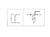
- FIG. 10A and FIG. 10B are diagrams showing a conventional example of a switched capacitor booster circuit using a switched capacitor.
- FIG. 10A shows a state when the capacitor is charged
- FIG. 10B shows a state when the capacitor is discharged.
- a switched capacitor (refer to the left side of FIGS. 10A and 10B) is configured by alternately repeating a state in which the capacitor is charged by switching the switch to the power supply side and a state in which the capacitor is discharged by switching the switch to the load side. This circuit supplies power to a load.
- a switched capacitor booster circuit (refer to the right side of FIGS. 10A and 10B) using this switched capacitor includes a plurality of capacitors. The capacitors are connected in parallel and charged, and the capacitors are connected in series and discharged. In this circuit, the input voltage is boosted and supplied to the load by alternately repeating the state.
- Non-Patent Document 1 can be cited as an example of the related art related to the above.
- the transformerless booster chopper of FIG. 9A When the transformerless booster chopper of FIG. 9A is used as the DC booster described above, the DC power can be boosted without AC conversion, but the input and output cannot be insulated. Therefore, when an accident current flows to the solar cell side, a high voltage of tens of thousands of volts is applied to the solar cell, and the solar cell may be severely damaged. In addition, in the transformerless step-up chopper of FIG. 9A, it is difficult to reverse the polarity during the step-up.
- the transformer booster circuit of FIG. 9B When the transformer booster circuit of FIG. 9B is used as the DC booster, the DC power generated by the solar cell array is once converted into AC power, and this AC power is boosted by a transformer. After that, it is necessary to convert it back to DC power again using an AC / DC converter (such as a thyristor valve), which causes a reduction in efficiency due to AC conversion and cannot be said to be a true DC / DC converter.
- an AC / DC converter such as a thyristor valve
- the capacitor is disconnected from the power supply when the capacitor is discharged, so that the capacitor can receive power from the power supply. Disappear.
- the power source is a solar cell
- the output end of the solar cell is opened and the power generation is stopped, so that the power generation efficiency is lowered.
- the capacitor is disconnected from the load when the capacitor is charged, the boosted output cannot be continuously performed from the capacitor.
- the present invention provides a DC booster capable of continuously boosting output while insulating input and output without using a transformer, and a photovoltaic power generation system using the same. With the goal.
- a DC booster according to the present invention has at least one boost DC / DC converter that boosts the output of a DC power supply, and the boost DC / DC converter uses charge / discharge of a capacitor.
- a transformer-less first capacitor booster circuit and a second capacitor booster circuit that perform a boosting operation, and a path changeover switch that switches each input / output path of the first capacitor booster circuit and the second capacitor booster circuit.
- each of the first capacitor booster circuit and the second capacitor booster circuit includes a plurality of capacitors, and each capacitor is connected in parallel and charged.
- a configuration (second configuration) that is a switched capacitor boosting circuit that boosts the input voltage supplied from the previous stage and supplies it to the subsequent stage by alternately repeating the state in which the capacitors are connected in series is discharged.
- the first capacitor booster circuit and the second capacitor booster circuit are controlled so that their charge / discharge states are reversed (third configuration). It is good to make it.
- the path changeover switch connects the charged state of the first capacitor booster circuit and the second capacitor booster circuit to the front stage and shuts off the rear stage.
- a configuration (fourth configuration) may be employed in which the input / output paths of the first capacitor booster circuit and the second capacitor booster circuit are switched so that the discharge state is connected to the subsequent stage and disconnected from the previous stage. .
- the path changeover switch may be configured to use an analog switch such as a relay (fifth configuration).
- the path changeover switch may be configured to use a semiconductor switch such as a power transistor or a thyristor (sixth configuration).
- the DC booster having any one of the first to sixth configurations may have a configuration (seventh configuration) further including a plurality of power storage devices that store DC power output from the boost DC / DC converter. .
- the DC booster having the seventh configuration at least one of the plurality of power storage devices is charged from the boost DC / DC converter, and at least another is discharged to the DC power system. In addition, it is preferable that each charge / discharge state is rotated (eighth configuration).
- the DC booster having any one of the first to eighth configurations is a cooling device that cools the first capacitor booster circuit, the second capacitor booster circuit, or the semiconductor switch that constitutes the path switch. It is good to make it the structure which has further (9th structure).
- the cooling device may be an electrical refrigeration device (tenth configuration).
- the cooling device may be configured to cool the semiconductor switch by immersing it in a refrigerant liquid (an eleventh configuration).
- the cooling device may be configured to use liquid nitrogen as the refrigerant liquid (a twelfth configuration).
- the cooling device may be configured to cool the semiconductor switches one by one (a thirteenth configuration).
- the cooling device may be configured to cool a plurality of the semiconductor switches together (fourteenth configuration).
- the cooling device may be configured to cool the boost DC / DC converters together (fifteenth configuration).
- the DC booster having any one of the first to fifteenth configurations, as the boost DC / DC converter, boosts an input voltage of 2 kV to 100 V to generate an output voltage of 30 kV to 3 kV.
- DC / DC converter a second boost DC / DC converter that boosts an input voltage of 30 kV to 3 kV to generate an output voltage of 250 kV to 60 kV, and an input voltage of 250 kV to 60 kV to boost an output of ⁇ 1000 kV to ⁇ 150 kV
- a configuration including a third step-up DC / DC converter that generates a voltage (sixteenth configuration) is preferable.
- a photovoltaic power generation system includes a solar cell array and a DC booster configured by any one of the first to sixteenth configurations for boosting the output of the solar cell array (a seventeenth aspect). Composition).
- the solar power generation system having the seventeenth configuration may be configured to have a voltage control device that performs voltage stability control and maximum power point tracking control (eighteenth configuration).
- the solar cell array may have a configuration (a nineteenth configuration) including a solar cell panel, a connection box, and a current collector. .
- the present invention it is possible to provide a DC booster capable of performing continuous boosting output while insulating between input and output without using a transformer, and a solar power generation system using the DC booster.
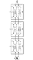
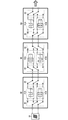
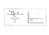
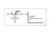
- Diagram showing the overall configuration of the photovoltaic power generation system The figure which shows 1st Embodiment of a photovoltaic power generation system (1st switching state) The figure which shows 1st Embodiment of a photovoltaic power generation system (2nd switching state) Conceptual diagram of switched capacitor booster circuit (charged state) Conceptual diagram of switched capacitor booster circuit (discharge state) The figure which shows 2nd Embodiment of a solar energy power generation system.
- FIG. 1 is a diagram illustrating an overall configuration of a photovoltaic power generation system.
- the photovoltaic power generation system of this configuration example includes a solar cell array 10 (hereinafter referred to as a PV [photovoltaic] array 10), a voltage control device 20, and step-up DC / DC converters 30 to 50.
- the configuration including the three-step boost DC / DC converters 30 to 50 will be described as an example.
- the photovoltaic power generation system of this configuration example has a configuration including at least one step-up DC / DC converter, and the number of boosting steps is not limited to a plurality of steps.
- a photovoltaic power generation system that obtains a 1 GW DC output by laying a PV array 10 on a power generation site of 5 km in length and 6 km in width
- 100 voltage control devices 20 and step-up DC / DC converters 30 are scattered in the power generation site.
- 10 step-up DC / DC converters 40 are scattered within the power generation site.
- the total length of electric wires (overhead transmission line, power cable, etc.) connecting the step-up DC / DC converter 30 and the step-up DC / DC converter 40 is about 1 km
- the total length of the electric wire connecting the step-up DC / DC converter 50 is about 3.9 km.
- the PV array 10 includes a solar cell panel 10A (hereinafter referred to as a PV panel 10A), a connection box 10B, and a current collector panel 10C.
- the PV panel 10A converts light energy into electrical energy (DC power) using the photovoltaic effect.
- the junction box 10B connects in parallel DC power input from the plurality of PV panels 10A or a string in which a plurality of PV panels 10A are connected in series, and outputs the DC power to the subsequent stage.
- the current collector panel 10C connects the DC power input from the plurality of connection boxes 10B in parallel and outputs the DC power to the subsequent stage. In this way, a total of 10 MW of power is collected to the subsequent voltage control device 20.
- the connection box 10B and the current collector panel 10C may be omitted.
- the voltage control device 20 receives the DC power input from the PV array 10 and performs voltage stability control and maximum power point tracking control (so-called MPPT [maximum power point tracking] control).
- the step-up DC / DC converter 30 boosts a direct-current voltage (for example, DC 1 kV) input from the voltage control device 20 at a predetermined boost ratio (for example, 1:10) to generate a first boost voltage (for example, DC 10 kV).
- the value of the input DC voltage is set so as to be DC 1 kV depending on the specifications of the PV array 10 and the number of strings in series, but the above voltage value and boost ratio are only examples, and the boost DC / DC converter 30 is 2 kV. Any device that boosts an input voltage of ⁇ 100 V (preferably 1.5 kV to 200 V) and generates an output voltage of 30 kV to 3 kV (preferably 20 kV to 6 kV) may be used.
- the output power from the step-up DC / DC converter 30 is transmitted by electric wires to the position of the next step-up DC / DC converter 40 by 10 routes, and connected in parallel before the step-up DC / DC converter 40 is input.
- the current is collected to a total of 100 MW and then input to the step-up DC / DC converter 40.
- the step-up DC / DC converter 40 boosts the first boosted voltage (for example, DC 10 kV) at a predetermined boost ratio (for example, 1:10) to generate the second boosted voltage (for example, DC 100 kV).
- the above voltage values and boost ratios are examples, and the boost DC / DC converter 40 boosts an input voltage of 30 kV to 3 kV (preferably 20 kV to 6 kV) and outputs an output voltage of 250 kV to 60 kV (preferably 150 kV to 100 kV). As long as it generates
- the output power (10 routes) from the step-up DC / DC converter 40 is transmitted by electric wires to the position of the next step-up DC / DC converter 50 and connected in parallel before the input of the step-up DC / DC converter 50 to total. After collecting the current to 1 GW, the voltage is input to the step-up DC / DC converter 50.
- the step-up DC / DC converter 50 boosts the second boosted voltage (for example, DC 100 kV) at a predetermined boost ratio (for example, 1: 5) to generate a third boosted voltage (for example, DC ⁇ 500 kV).
- the above voltage values and step-up ratios are examples, and the step-up DC / DC converter 50 boosts the input voltage of 250 kV to 60 kV (preferably 150 kV to 100 kV) to ⁇ 1000 kV to ⁇ 150 kV (preferably ⁇ 800 kV to ⁇ 250 kV). ) That generates the output voltage of ().
- the total generated power obtained by the PV array 10 can be boosted to an appropriate voltage value, then output to the DC power system, and transmitted toward the demand area. .
- the step-up DC / DC converter 30 includes capacitor step-up circuits 31A and 31B, an input side path switch 32, and an output side path switch 33.
- the step-up DC / DC converter 40 includes capacitor step-up circuits 41A and 41B, an input side path switch 42, and an output side path switch 43.
- the step-up DC / DC converter 50 includes capacitor step-up circuits 51A and 51B, an input side path changeover switch 52, and an output side path changeover switch 53.
- Capacitor boosting circuits 31A and 31B each perform a boosting operation without a transformer using charging and discharging of the capacitor.
- each of the capacitor boosting circuits 31A and 31B includes a plurality of capacitors, and alternately repeats a state in which the capacitors are connected in parallel and a state in which the capacitors are connected in series and a state in which the capacitors are connected in series.
- This is a switched capacitor booster circuit (see FIGS. 3A and 3B) that boosts the input voltage supplied from the previous stage and supplies it to the subsequent stage.
- Capacitor booster circuits 31A and 31B are controlled so that their charge / discharge states are reversed.
- the configurations and operations of the capacitor boost circuits 41A and 41B and the capacitor boost circuits 51A and 51B are basically the same as described above.
- the boost multiple of the capacitor boost circuit 31A and the number of capacitors do not simply match. Between the capacitor booster circuit 31A and the capacitor booster circuit 41A at the subsequent stage, no current flows when the input / output voltages of both circuits coincide. Therefore, the number of capacitors and the capacitor capacity of the capacitor booster circuit 31A may be set as appropriate so that the input / output voltage ratio of the capacitor booster circuit 31A in the current stop state becomes a desired booster ratio.
- the capacitor boost circuits 31B, 41A, and 41B are basically the same as described above.
- the input side path changeover switch 32 switches the input paths of the capacitor booster circuits 31A and 31B.
- the output side path switch 33 switches each output path of the capacitor booster circuits 31A and 31B. More specifically, the input side path changeover switch 32 and the output side path changeover switch 33 connect one of the capacitor boost circuits 31A and 31B that is in a charged state to the previous stage and cut off from the subsequent stage, while being in a discharged state. Each of the input / output paths of the capacitor booster circuits 31A and 31B is switched so that the one is connected to the subsequent stage and is cut off from the previous stage.
- the configuration and operation of the input side path changeover switches 42 and 52 and the output side path changeover switches 43 and 53 are basically the same as described above.
- the boosting operation of the boosting DC / DC converters 30 to 50 will be described.
- the power generation output (10 MW-1 kV) of the PV array 10 is the input side path changeover switch of the step-up DC / DC converter 30.
- the voltage is supplied to the capacitor booster circuit 31A via the reference numeral 32.
- the capacitor booster circuit 31A is charged by connecting a plurality of capacitors in parallel.
- the capacitor boosting circuit 31A enters a state of discharging a plurality of capacitors connected in series (step-up output state).
- the boost output of the capacitor boost circuit 31A is supplied to the capacitor boost circuit 41A via the output side path switch 33 of the boost DC / DC converter 30 and the input path switch 42 of the boost DC / DC converter 40.
- the capacitor booster circuit 41A is charged by connecting a plurality of capacitors in parallel.
- the capacitor boosting circuit 41A enters a state of discharging a plurality of capacitors connected in series (step-up output state).
- the boost output of the capacitor boost circuit 41A is supplied to the capacitor boost circuit 51A via the output side path switch 43 of the boost DC / DC converter 40 and the input path switch 52 of the boost DC / DC converter 50.
- the capacitor booster circuit 51A is charged by connecting a plurality of capacitors in parallel.
- the capacitor boosting circuit 51A enters a state of discharging a plurality of capacitors connected in series (step-up output state).
- the boost output of the capacitor boost circuit 51A is sent to the DC power system via the output side path switch 53 of the boost DC / DC converter 30.
- the generated power obtained by the PV array 10 is converted into an appropriate voltage value (for example, The voltage can be boosted to ⁇ 500 kV) and output to the DC power system.
- boost DC / DC converters 30 to 50 it is possible to realize a transformer-less boost circuit by adopting a switched capacitor boost circuit that has been used in the field of weak electricity such as a signal processing circuit. It is possible to obtain a desired boosted voltage without causing a reduction in efficiency due to AC conversion.
- each of the boost DC / DC converters 30 to 50 has the first system capacitor booster circuit.
- a second system capacitor booster circuit (31B, 41B, 51B) is provided in parallel with the circuit (31A, 41A, 51A), and a boost operation using the second system capacitor booster circuit (31B, 41B, 51B) is provided. Are also performed in parallel.
- the boost DC / DC converters 30 to 50 are in the second switching state (see FIG. 2B)
- the power generation output (10 MW-1 kV) of the PV array 10 is the boost DC / DC converter 30.
- the capacitor booster circuit 31B is charged by connecting a plurality of capacitors in parallel.
- the capacitor boosting circuit 31B enters a state of discharging a plurality of capacitors connected in series (step-up output state).
- the boosted output of the capacitor booster circuit 31B is supplied to the capacitor booster circuit 41B via the output side path selector switch 33 of the booster DC / DC converter 30 and the input side path selector switch 42 of the booster DC / DC converter 40.
- the capacitor booster circuit 41B is in a state of charging by connecting a plurality of capacitors in parallel.
- the capacitor boosting circuit 41B enters a state of discharging a plurality of capacitors connected in series (step-up output state).
- the boost output of the capacitor boost circuit 41B is supplied to the capacitor boost circuit 51B via the output side path switch 43 of the boost DC / DC converter 40 and the input path switch 52 of the boost DC / DC converter 50.
- the capacitor booster circuit 51B is charged by connecting a plurality of capacitors in parallel.
- the capacitor boosting circuit 51B enters a state of discharging a plurality of capacitors connected in series (step-up output state).
- the boosted output of the capacitor booster circuit 51B is sent to the DC power system via the output side path switch 53 of the boost DC / DC converter 30.
- the charge / discharge state of the first system capacitor boost circuit (31A, 41A, 51A) and the second system capacitor boost circuit (31B, 41B and 51B) are mutually reversed.
- the capacitor booster circuit of one system can be in a charged state while the capacitor booster circuit of the other system can be in a discharged state.
- the boost DC / DC converters 30 to 50 are respectively provided with input side path change-over switches 32, 42, 52 and output side path change-over switches 33, 43, 53, so that the capacitor boost circuit in a charged state is provided. Is connected to the previous stage and shut off from the subsequent stage, while switching control of the input / output path is performed so that the capacitor booster circuit in a discharged state is connected to the subsequent stage and shut off from the previous stage. With such a configuration, it is possible to insulate circuit between the PV array 10 at the front stage and the DC power system at the rear stage without using a transformer.
- an analog switch such as a relay may be used, or a semiconductor switch such as a power transistor or a thyristor may be used.
- a semiconductor switch it cannot be said that the input and output are electrically isolated, so that in the event of a problem, there is a possibility that an excessive current will flow backward from the output side to the input side. Therefore, it is desirable to use an analog switch such as a relay if the input and output are more reliably insulated.
- a semiconductor switch such as a power transistor when priority is given to preventing the destruction of the switch element, such as when the applied voltage is very high.
- the photovoltaic power generation system of the first embodiment it is possible to perform continuous boost output while insulating the input and output without using a transformer.
- FIG. 4 is a diagram illustrating a second embodiment of the solar power generation system.
- the photovoltaic power generation system of the second embodiment further includes direct current power output from the final boost DC / DC converter 50 (for example, There are a plurality of (two in FIG. 4) power storage devices 60A and 60B that store ( ⁇ 500 kV).
- the output voltage of the boost DC / DC converter 50 in the final stage is assumed to decrease in a relatively short time due to the characteristics of the capacitor. Therefore, in the photovoltaic power generation system of the first embodiment, it may be difficult to stabilize the output power to the DC power system.
- the plurality of power storage devices 60A and 60B are installed as power buffers, and the power storage devices 60A and 60B are configured to transmit power from the charged power storage devices to the DC power system 70.
- a configuration that performs 60B rotation is employed. With such a configuration, power transmission to the DC power system 70 can be stabilized.
- FIGS. 5A to 5C are diagrams showing a modification of the second embodiment (when three power storage devices 60A to 60C are installed), respectively.
- Each of the three power storage devices 60A to 60C is charged / discharged so that at least one of the power storage devices 60A to 60C is charged from the boost DC / DC converter 50 in the final stage and at least another is discharged to the DC power system 70. Is rotated.
- the state shifts to the third rotation state of FIG. 5C.
- the output power of power storage device 60A that has been fully charged in the previous rotation state (see FIG. 5A) while charging power storage device 60B using the output power of step-up DC / DC converter 50. Is used to transmit power to the DC power system 70.
- the power storage device 60C that has been fully charged in the previous rotation state (see FIG. 5B) is in a standby state in preparation for discharging in the next rotation state (see FIG. 5A).
- the power storage device it is desirable that three or more power storage devices be installed so that power transmission from the power storage device to the DC power system 70 can be maintained even when power generation in the PV array 10 is stopped, such as at night. From the viewpoint of stability (particularly voltage stability), it is desirable to install four or more power storage devices having charge / discharge characteristics capable of rapid charge and low-speed discharge. Note that a state other than the power storage device being charged and the power storage device being transmitted may be set in a standby state. Whether the standby power storage device is fully charged or discharged (waiting for charging) may be determined by the operation of the photovoltaic power generation system.
- a power storage device with a capacity as large as possible (ideally a 1 GW-500 kV class ultra-large power storage device) such as a large-capacity capacitor or NAS battery.
- FIG. 6A and FIG. 6B are diagrams each showing a configuration example (three times boost type) of the switched capacitor boost circuit.
- FIG. 6A shows a state when the capacitor is charged
- FIG. 6B shows a state when the capacitor is discharged.
- the switched capacitor booster circuit of this configuration example includes capacitors C11 to C13 and semiconductor switches SW10 to SW19.
- the switch SW10 conducts / cuts off between the first input terminal T11 and the first end of the capacitor C11.
- the switch SW11 conducts / cuts off between the second input terminal T12 and the second end of the capacitor C11.
- Switch SW12 conducts / cuts off between the second end of capacitor C11 and the second end of capacitor C12.
- Switch SW13 conducts / cuts off between the first end of capacitor C11 and the second end of capacitor C12.
- the switch SW14 conducts / cuts off between the first end of the capacitor C11 and the first end of the capacitor C12.
- Switch SW15 conducts / cuts off between the second end of capacitor C12 and the second end of capacitor C13.
- Switch SW16 conducts / cuts off between the first end of capacitor C12 and the second end of capacitor C13.
- Switch SW17 conducts / cuts off between the first end of capacitor C12 and the first end of capacitor C13.
- the switch SW18 conducts / cuts off between the first end of the capacitor C13 and the first output terminal T13.
- the switch SW19 conducts / cuts off between the second end of the capacitor C11 and the second output terminal T14.
- the switches SW10 to SW12, the switch SW14, the switch SW15, and the switch SW17 are turned on, and the switch SW13, the switch SW16, the switch SW18, and the switch SW19 are turned off.
- the capacitors C11 to C13 are connected in parallel between the first input terminal T11 and the second input terminal T12.
- the switches SW10 to SW12, the switch SW14, the switch SW15, and the switch SW17 are turned off, and the switch SW13, the switch SW16, the switch SW18, and the switch SW19 are turned on.
- the capacitors C11 to C13 are connected in series between the first output terminal T13 and the second output terminal T14.
- the number of necessary switch elements increases as the boost ratio increases.
- the switch element forming the switched capacitor booster circuit is required to have a fast on / off response, it is necessary to use a semiconductor switch such as a power transistor or a thyristor.
- the on-resistance of the semiconductor switch has a positive temperature characteristic (see FIG. 7). Therefore, it is considered effective to cool the semiconductor switch in order to avoid a decrease in power transmission efficiency due to an increase in the number of switch elements (and hence an increase in on-resistance).
- FIG. 8 is a diagram showing a third embodiment of the solar power generation system.
- the solar power generation system of the third configuration example includes the capacitor booster circuit (31A, 31B, 41A, 41B, 51A, 52B) and the path switch (32, 33, 42, 43, 52, 53) described above. It further includes a cooling device 80A or 80B that constantly cools the semiconductor switch to be configured.
- the cooling device is not a water cooling type cooling device applied to a conventional thyristor valve, but a cooling device capable of cooling the semiconductor switch more powerfully, for example, an electric refrigeration device 80A (left side in FIG. 8) It is desirable to employ a cooling device 80B (right side in FIG. 8) that cools the semiconductor switch by directly immersing it in a cryogenic refrigerant liquid (liquid nitrogen or the like).
- a cryogenic refrigerant liquid liquid nitrogen or the like.
- the cooling device 80B using liquid nitrogen can be realized with a simple structure and has already been applied to a semiconductor manufacturing apparatus or the like. There seems to be little problem.
- the type of refrigerant liquid is not limited to liquid nitrogen.
- the cooling devices 80A and 80B may be configured to cool the semiconductor switches one by one as shown in FIG. 8, or a plurality of semiconductor switches are gathered together as shown by the broken lines in FIGS. 6A and 6B. It is good also as a structure to cool.
- the cooling devices 80A and 80B may be configured to cool the step-up DC / DC converters 30 to 50 together.
- the semiconductor switch is cooled strongly, the on-resistance of the semiconductor switch can be reduced and the power transfer efficiency can be increased, so the conversion efficiency of the switched capacitor booster circuit using a large number of semiconductor switches can be improved. (Low power loss) can be realized.
- a transformer is used for AC transformation, it is necessary to insert an orthogonal transformer and an AC / DC converter before and after the transformer, respectively, and the conversion efficiency of the entire unit is 95% or less. If a structure is employ
- the DC booster according to the present invention can be used, for example, as a substation facility in a large-scale solar power plant (for example, a gigawatt class or a megawatt class). Further, the DC booster according to the present invention can be widely applied to other power networks such as a household solar power generation system and a small smart grid.
- the DC booster according to the present invention is not only a DC booster for a solar power generation system, but also, for example, a DC power generation system using renewable energy such as wind power, a DC power generation system using a rotating machine, or It can also be suitably used as a DC boosting means for a DC power supply system using a fuel cell, a storage battery or the like. Further, the DC booster according to the present invention can be suitably mounted on a train, an electric vehicle, and the like.
Landscapes
- Engineering & Computer Science (AREA)
- Power Engineering (AREA)
- Photovoltaic Devices (AREA)
- Dc-Dc Converters (AREA)
- Charge And Discharge Circuits For Batteries Or The Like (AREA)
Abstract
本発明に係る直流昇圧装置は、直流電源(10)の出力を昇圧する少なくとも一段(図2Aでは3段)の昇圧DC/DCコンバータ(30、40、50)を有し、昇圧DC/DCコンバータ(30、40、50)は、それぞれ、キャパシタの充放電を利用して昇圧動作を行うトランスレスの第1キャパシタ昇圧回路(31A、41A、51A)及び第2キャパシタ昇圧回路(31B、41B、51B)と、第1キャパシタ昇圧回路(31A、41A、51A)及び第2キャパシタ昇圧回路(31B、41B、51B)の各入出力経路を切り替える経路切替スイッチ(32、33、42、43、52、53)を含む。
Description
本発明は、直流昇圧装置及びこれを用いた太陽光発電システムに関するものである。
図9Aは、トランスレス昇圧チョッパの一従来例を示す図である。本従来例のトランスレス昇圧チョッパは、スイッチとリアクトル(コイル)とダイオードを組み合わせた回路であり、直流入力電圧DCINを昇圧して直流出力電圧DCOUTを生成する。なお、本従来例のトランスレス昇圧チョッパは、例えば、弱電向け(信号処理回路向け)の電源回路として用いられる。
図9Bは、トランス昇圧回路の一従来例を示す図である。本従来例のトランス昇圧回路は、スイッチング素子を用いて直流入力電圧DCINを一旦パルス波形(交流電力)に変換し、この交流電力を高周波トランスで昇圧した後、再び直流電力に変換し直すことで、直流出力電圧DCOUTを生成する。なお、本従来例のトランス昇圧回路は、例えば、太陽光発電システムのパワーコンディショナにおいて、最大電力点追従制御などを実施するために使用される。
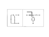
図10Aと図10Bは、スイッチトキャパシタを応用したスイッチトキャパシタ昇圧回路の一従来例を示す図である。なお、図10Aはキャパシタ充電時の様子を示しており、図10Bはキャパシタ放電時の様子を示している。スイッチトキャパシタ(図10A、図10Bの左側を参照)は、スイッチを電源側に切り替えてキャパシタを充電する状態と、スイッチを負荷側に切り替えてキャパシタを放電する状態と、を交互に繰り返すことにより、負荷に電力を供給する回路である。このスイッチトキャパシタを応用したスイッチトキャパシタ昇圧回路(図10A、図10Bの右側を参照)は、複数のキャパシタを含み、各キャパシタを並列接続して充電する状態と、各キャパシタを直列接続して放電する状態と、を交互に繰り返すことにより、入力電圧を昇圧して負荷に供給する回路である。
なお、上記に関連する従来技術の一例としては、非特許文献1を挙げることができる。
「大容量キャパシタを用いたEVの効率的充放電制御の検討」、電気学会自動車研究会, VT-07-20, 2007.12.11(東京大学)
近年、大規模な太陽光発電システム(例えばMW級のメガソーラー発電所)の建設が世界中で推進されている。このような太陽光発電システムでは、太陽電池アレイで発電された直流電力を交流電力系統(77kV、3相交流の特別高圧送電線など)に連系させて送電が行われている。一方、大電力を長距離送電することを目的とした直流電力系統も導入実績が拡大しつつあり、この直流電力系統へ大規模な太陽光発電システムを連系させることも今後視野に入れる必要がある。直流電力系統への連系に際しては、太陽電池アレイで発電された直流電力を交流電力に変換することなく昇圧することのできる直流昇圧装置を使うことが好ましい。
上記の直流昇圧装置として、図9Aのトランスレス昇圧チョッパを用いた場合には、AC変換を介することなく直流電力の昇圧を行うことができるが、入出力間を絶縁することができなくなる。従って、事故電流が太陽電池側に流れた場合には、太陽電池に数万Vもの高電圧が加わって、太陽電池が大破してしまうおそれがある。また、図9Aのトランスレス昇圧チョッパでは、昇圧途中での極性反転も困難となる。
また、上記の直流昇圧装置として、図9Bのトランス昇圧回路を用いた場合には、太陽電池アレイで発電された直流電力を一旦交流電力に変換し、この交流電力を変圧器(トランス)で昇圧した後、交直変換器(サイリスタバルブなど)を用いて再び直流電力に変換し直す必要があり、AC変換に伴う効率低下が生じる上、本当の意味でのDC/DCコンバータとは言えない。
また、上記の直流昇圧装置として、図10A及び図10Bのスイッチトキャパシタ昇圧回路を用いた場合には、キャパシタの放電時にキャパシタが電源から切り離されるので、キャパシタで電源からの電力供給を受けることができなくなる。電源が太陽電池の場合には、太陽電池の出力端が開放となって発電が停止することになるので、発電効率が低下してしまう。また、キャパシタの充電時にはキャパシタが負荷から切り離されるので、キャパシタから継続的に昇圧出力を行うことができなくなる。
本発明は、上記の問題点に鑑み、トランスを用いることなく入出力間を絶縁しながら継続的な昇圧出力を行うことが可能な直流昇圧装置及びこれを用いた太陽光発電システムを提供することを目的とする。
上記目的を達成するために、本発明に係る直流昇圧装置は、直流電源の出力を昇圧する少なくとも一段の昇圧DC/DCコンバータを有し、前記昇圧DC/DCコンバータは、キャパシタの充放電を利用して昇圧動作を行うトランスレスの第1キャパシタ昇圧回路及び第2キャパシタ昇圧回路と、前記第1キャパシタ昇圧回路と前記第2キャパシタ昇圧回路の各入出力経路を切り替える経路切替スイッチと、を含む構成(第1の構成)とされている。
なお、上記第1の構成から成る直流昇圧装置において、前記第1キャパシタ昇圧回路と前記第2キャパシタ昇圧回路は、それぞれ、複数のキャパシタを含み、各キャパシタを並列接続して充電する状態と、各キャパシタを直列接続して放電する状態と、を交互に繰り返すことにより、前段から供給される入力電圧を昇圧して後段に供給するスイッチトキャパシタ昇圧回路である構成(第2の構成)にするとよい。
また、上記第2の構成から成る直流昇圧装置において、前記第1キャパシタ昇圧回路と前記第2キャパシタ昇圧回路は、互いの充放電状態が逆となるように制御される構成(第3の構成)にするとよい。
また、上記第3の構成から成る直流昇圧装置において、前記経路切替スイッチは前記第1キャパシタ昇圧回路と前記第2キャパシタ昇圧回路のうち、充電状態である方を前段と接続して後段から遮断する一方、放電状態である方を後段と接続して前段から遮断するように、前記第1キャパシタ昇圧回路と前記第2キャパシタ昇圧回路の各入出力経路を切り替える構成(第4の構成)にするとよい。
また、上記第1~第4いずれかの構成から成る直流昇圧装置において、前記経路切替スイッチはリレーなどのアナログスイッチを用いて成る構成(第5の構成)にするとよい。
また、上記第1~第4いずれかの構成から成る直流昇圧装置において、前記経路切替スイッチは、パワートランジスタやサイリスタなどの半導体スイッチを用いて成る構成(第6の構成)にするとよい。
また、上記第1~第6いずれかの構成から成る直流昇圧装置は、前記昇圧DC/DCコンバータから出力される直流電力を蓄える複数の蓄電装置をさらに有する構成(第7の構成)にするとよい。
また、上記第7の構成から成る直流昇圧装置において、前記複数の蓄電装置は、少なくとも一つが前記昇圧DC/DCコンバータからの充電を行い、少なくとも別の一つが直流電力系統への放電を行うように、各々の充放電状態がローテーションされる構成(第8の構成)にするとよい。
また、上記第1~第8いずれかの構成から成る直流昇圧装置は、前記第1キャパシタ昇圧回路及び前記第2キャパシタ昇圧回路、乃至は、前記経路切替スイッチを構成する半導体スイッチを冷却する冷却装置をさらに有する構成(第9の構成)にするとよい。
また、上記第9の構成から成る直流昇圧装置において、前記冷却装置は、電気的な冷凍装置である構成(第10の構成)にするとよい。
また、上記第9の構成から成る直流昇圧装置において、前記冷却装置は、前記半導体スイッチを冷媒液に浸して冷却する構成(第11の構成)にするとよい。
また、上記第11の構成から成る直流昇圧装置において、前記冷却装置は、前記冷媒液として液体窒素を用いる構成(第12の構成)にするとよい。
また、上記第9~第12いずれかの構成から成る直流昇圧装置において、前記冷却装置は、前記半導体スイッチを一つずつ冷却する構成(第13の構成)にするとよい。
また、上記第9~第12いずれかの構成から成る直流昇圧装置において、前記冷却装置は、前記半導体スイッチを複数まとめて冷却する構成(第14の構成)にするとよい。
また、上記第9~第12いずれかの構成から成る直流昇圧装置において、前記冷却装置は、前記昇圧DC/DCコンバータをまとめて冷却する構成(第15の構成)にするとよい。
また、上記第1~第15いずれかの構成から成る直流昇圧装置は、前記昇圧DC/DCコンバータとして、2kV~100Vの入力電圧を昇圧して30kV~3kVの出力電圧を生成する第1昇圧DC/DCコンバータと、30kV~3kVの入力電圧を昇圧して250kV~60kVの出力電圧を生成する第2昇圧DC/DCコンバータと、250kV~60kVの入力電圧を昇圧して±1000kV~±150kVの出力電圧を生成する第3昇圧DC/DCコンバータを含む構成(第16の構成)にするとよい。
また、本発明に係る太陽光発電システムは、太陽電池アレイと、前記太陽電池アレイの出力を昇圧する上記第1~第16いずれかの構成から成る直流昇圧装置と、を有する構成(第17の構成)とされている。
また、上記第17の構成から成る太陽光発電システムは、電圧安定制御と最大電力点追従制御を行う電圧制御装置を有する構成(第18の構成)にするとよい。
また、上記第17または第18の構成から成る太陽光発電システムにおいて、前記太陽電池アレイは、太陽電池パネルと、接続箱と、集電盤と、を含む構成(第19の構成)にするとよい。
本発明によれば、トランスを用いることなく入出力間を絶縁しながら継続的な昇圧出力を行うことが可能な直流昇圧装置及びこれを用いた太陽光発電システムを提供することが可能となる。
以下では、1GWの発電容量を有する太陽光発電システムの直流昇圧装置について、本発明を適用した構成を例に挙げて説明を行う。
<全体構成>
図1は、太陽光発電システムの全体構成を示す図である。本構成例の太陽光発電システムは、太陽電池アレイ10(以下では、PV[photovoltaic]アレイ10と呼ぶ)と、電圧制御装置20と、昇圧DC/DCコンバータ30~50とを有する。なお、以下では、3段の昇圧DC/DCコンバータ30~50を備えた構成を例に挙げて説明を行うが、例えば発電容量が1MW程度までであれば、5kV~20kVへの昇圧出力で済むため、昇圧DC/DCコンバータを1段だけ備えれば足りる場合も想定される。すなわち、本構成例の太陽光発電システムは、少なくとも一段の昇圧DC/DCコンバータを有する構成であって、昇圧段数は複数段に限定されるものではない。
図1は、太陽光発電システムの全体構成を示す図である。本構成例の太陽光発電システムは、太陽電池アレイ10(以下では、PV[photovoltaic]アレイ10と呼ぶ)と、電圧制御装置20と、昇圧DC/DCコンバータ30~50とを有する。なお、以下では、3段の昇圧DC/DCコンバータ30~50を備えた構成を例に挙げて説明を行うが、例えば発電容量が1MW程度までであれば、5kV~20kVへの昇圧出力で済むため、昇圧DC/DCコンバータを1段だけ備えれば足りる場合も想定される。すなわち、本構成例の太陽光発電システムは、少なくとも一段の昇圧DC/DCコンバータを有する構成であって、昇圧段数は複数段に限定されるものではない。
例えば、縦5km×横6kmの発電サイトにPVアレイ10を敷き詰めて1GWのDC出力を得る太陽光発電システムでは、電圧制御装置20及び昇圧DC/DCコンバータ30を発電サイト内に100か所点在させ、昇圧DC/DCコンバータ40を同発電サイト内に10か所点在させることになる。また、同規模の発電サイトでは、昇圧DC/DCコンバータ30と昇圧DC/DCコンバータ40とを接続する電線(架空送電線や電力ケーブルなど)の総延長が1km程度となり、昇圧DC/DCコンバータ40と昇圧DC/DCコンバータ50とを接続する電線の総延長が3.9km程度となる。
PVアレイ10は、太陽電池パネル10A(以下、PVパネル10Aと呼ぶ)と、接続箱10Bと、集電盤10Cと、を含む。PVパネル10Aは、光起電力効果を利用して光エネルギを電気エネルギ(直流電力)に変換する。接続箱10Bは、複数のPVパネル10Aまたはそれらを複数枚直列接続させたストリングスから入力される直流電力を並列接続させて後段に出力する。集電盤10Cは、複数の接続箱10Bから入力される直流電力を並列接続させて後段に出力する。このようにして、後段の電圧制御装置20へ合計10MW分の電力を集電する。なお、システムの構成によっては、接続箱10Bや集電盤10Cが省略されることもある。
電圧制御装置20は、PVアレイ10から入力される直流電力を受けて、その電圧安定制御と最大電力点追従制御(いわゆるMPPT[maximum power point tracking]制御)を行う。
昇圧DC/DCコンバータ30は、電圧制御装置20から入力される直流電圧(例えばDC1kV)を所定の昇圧比(例えば1:10)で昇圧して第1昇圧電圧(例えばDC10kV)を生成する。入力される直流電圧の値は、PVアレイ10の仕様やストリングスの直列数によってDC1kVとなるように設定するが、上記の電圧値や昇圧比は例示であり、昇圧DC/DCコンバータ30は、2kV~100V(好ましくは1.5kV~200V)の入力電圧を昇圧して30kV~3kV(好ましくは20kV~6kV)の出力電圧を生成するものであればよい。
次に、昇圧DC/DCコンバータ30からの出力電力を各10ルートずつ、次段の昇圧DC/DCコンバータ40の位置まで電線により送電し、昇圧DC/DCコンバータ40の入力前において並列接続させて合計100MWに集電した後に昇圧DC/DCコンバータ40へ入力する。
昇圧DC/DCコンバータ40は、第1昇圧電圧(例えばDC10kV)を所定の昇圧比(例えば1:10)で昇圧して第2昇圧電圧(例えばDC100kV)を生成する。上記の電圧値や昇圧比は例示であり、昇圧DC/DCコンバータ40は、30kV~3kV(好ましくは20kV~6kV)の入力電圧を昇圧して250kV~60kV(好ましくは150kV~100kV)の出力電圧を生成するものであればよい。
さらに、昇圧DC/DCコンバータ40からの出力電力(10ルート)を、次段の昇圧DC/DCコンバータ50の位置まで電線により送電し、昇圧DC/DCコンバータ50の入力前において並列接続させて合計1GWに集電した後に昇圧DC/DCコンバータ50へ入力する。
昇圧DC/DCコンバータ50は、第2昇圧電圧(例えばDC100kV)を所定の昇圧比(例えば1:5)で昇圧して第3昇圧電圧(例えばDC±500kV)を生成する。上記の電圧値や昇圧比は例示であり、昇圧DC/DCコンバータ50は、250kV~60kV(好ましくは150kV~100kV)の入力電圧を昇圧して±1000kV~±150kV(好ましくは±800kV~±250kV)の出力電圧を生成するものであればよい。
本構成例の太陽光発電システムによれば、PVアレイ10で得られたトータルの発電電力を適切な電圧値まで昇圧した上で直流電力系統に出力し、需要地に向けて送電することができる。
以下では、上記構成例の太陽光発電システムについて、第1~第3実施形態を参照しながら、その要部の構成や動作を具体的に説明する。
<第1実施形態>
図2A及び図2Bは、いずれも、太陽光発電システムの第1実施形態(特に昇圧DC/DCコンバータ30~50の内部構成)を示す図である。昇圧DC/DCコンバータ30は、キャパシタ昇圧回路31A及び31Bと、入力側経路切替スイッチ32と、出力側経路切替スイッチ33と、を含む。昇圧DC/DCコンバータ40は、キャパシタ昇圧回路41A及び41Bと、入力側経路切替スイッチ42と、出力側経路切替スイッチ43と、を含む。昇圧DC/DCコンバータ50は、キャパシタ昇圧回路51A及び51Bと、入力側経路切替スイッチ52と、出力側経路切替スイッチ53と、を含む。
図2A及び図2Bは、いずれも、太陽光発電システムの第1実施形態(特に昇圧DC/DCコンバータ30~50の内部構成)を示す図である。昇圧DC/DCコンバータ30は、キャパシタ昇圧回路31A及び31Bと、入力側経路切替スイッチ32と、出力側経路切替スイッチ33と、を含む。昇圧DC/DCコンバータ40は、キャパシタ昇圧回路41A及び41Bと、入力側経路切替スイッチ42と、出力側経路切替スイッチ43と、を含む。昇圧DC/DCコンバータ50は、キャパシタ昇圧回路51A及び51Bと、入力側経路切替スイッチ52と、出力側経路切替スイッチ53と、を含む。
キャパシタ昇圧回路31A及び31Bは、それぞれ、キャパシタの充放電を利用してトランスレスで昇圧動作を行う。具体的に述べると、キャパシタ昇圧回路31A及び31Bは、それぞれ、複数のキャパシタを含み、各キャパシタを並列接続して充電する状態と、各キャパシタを直列接続して放電する状態と、を交互に繰り返すことにより、前段から供給される入力電圧を昇圧して後段に供給するスイッチトキャパシタ昇圧回路(図3A及び図3Bを参照)である。キャパシタ昇圧回路31A及び31Bは、互いの充放電状態が逆となるように制御される。キャパシタ昇圧回路41A及び41B、並びに、キャパシタ昇圧回路51A及び51Bについても、その構成や動作は基本的に上記と同様である。
なお、キャパシタ昇圧回路31Aの昇圧倍数とキャパシタ数は単純に一致しない。キャパシタ昇圧回路31Aと後段のキャパシタ昇圧回路41Aとの間では、両回路の入出力電圧が一致したときに電流が流れなくなる。従って、キャパシタ昇圧回路31Aのキャパシタ数やキャパシタ容量は、上記の電流停止状態におけるキャパシタ昇圧回路31Aの入出力電圧比が所望の昇圧比となるように適宜設定すればよいことになる。キャパシタ昇圧回路31B、41A、及び、41Bについても基本的に上記と同様である。
入力側経路切替スイッチ32は、キャパシタ昇圧回路31A及び31Bの各入力経路を切り替える。出力側経路切替スイッチ33は、キャパシタ昇圧回路31A及び31Bの各出力経路を切り替える。より具体的に述べると、入力側経路切替スイッチ32及び出力側経路切替スイッチ33は、キャパシタ昇圧回路31A及び31Bのうち、充電状態である方を前段と接続して後段から遮断する一方、放電状態である方を後段と接続して前段から遮断するように、キャパシタ昇圧回路31A及び31Bの各入出力経路を切り替える。入力側経路切替スイッチ42及び52、並びに、出力側経路切替スイッチ43及び53についても、その構成や動作については基本的に上記と同様である。
次に、昇圧DC/DCコンバータ30~50の昇圧動作について説明する。昇圧DC/DCコンバータ30~50が第1切替状態(図2Aを参照)とされている場合、PVアレイ10の発電出力(10MW-1kV)は、昇圧DC/DCコンバータ30の入力側経路切替スイッチ32を介してキャパシタ昇圧回路31Aに供給される。このとき、キャパシタ昇圧回路31Aは、複数のキャパシタを並列接続して充電する状態となる。
その後、昇圧DC/DCコンバータ30~50が第2切替状態(図2Bを参照)に切り替えられると、キャパシタ昇圧回路31Aは、複数のキャパシタを直列接続して放電する状態(昇圧出力状態)となり、キャパシタ昇圧回路31Aの昇圧出力は、昇圧DC/DCコンバータ30の出力側経路切替スイッチ33と、昇圧DC/DCコンバータ40の入力側経路切替スイッチ42を介して、キャパシタ昇圧回路41Aに供給される。このとき、キャパシタ昇圧回路41Aは、複数のキャパシタを並列接続して充電する状態となる。
その後、昇圧DC/DCコンバータ30~50が第1切替状態(図2Aを参照)に切り替えられると、キャパシタ昇圧回路41Aは、複数のキャパシタを直列接続して放電する状態(昇圧出力状態)となり、キャパシタ昇圧回路41Aの昇圧出力は、昇圧DC/DCコンバータ40の出力側経路切替スイッチ43と、昇圧DC/DCコンバータ50の入力側経路切替スイッチ52を介して、キャパシタ昇圧回路51Aに供給される。このとき、キャパシタ昇圧回路51Aは、複数のキャパシタを並列接続して充電する状態となる。
その後、昇圧DC/DCコンバータ30~50が第2切替状態(図2Bを参照)に切り替えられると、キャパシタ昇圧回路51Aは、複数のキャパシタを直列接続して放電する状態(昇圧出力状態)となり、キャパシタ昇圧回路51Aの昇圧出力は、昇圧DC/DCコンバータ30の出力側経路切替スイッチ53を介して、直流電力系統に送り出される。
このように、昇圧DC/DCコンバータ30~50であれば、上記の第1切替状態と第2切替状態を交互に繰り返すことにより、PVアレイ10で得られた発電電力を適切な電圧値(例えば±500kV)まで昇圧して直流電力系統に出力することができる。
また、昇圧DC/DCコンバータ30~50であれば、信号処理回路などの弱電分野で使用実績のあるスイッチトキャパシタ昇圧回路を採用することにより、昇圧回路のトランスレス化を実現することができるので、AC変換に伴う効率低下を招くことなく、所望の昇圧電圧を得ることが可能となる。
また、上記では、第1系統のキャパシタ昇圧回路(31A、41A、51A)に着目して昇圧動作の説明を行ったが、昇圧DC/DCコンバータ30~50は、それぞれ、第1系統のキャパシタ昇圧回路(31A、41A、51A)と並列に、第2系統のキャパシタ昇圧回路(31B、41B、51B)を備えており、第2系統のキャパシタ昇圧回路(31B、41B、51B)を用いた昇圧動作も同時並行的に行われる。
具体的に述べると、昇圧DC/DCコンバータ30~50が第2切替状態(図2Bを参照)とされている場合、PVアレイ10の発電出力(10MW-1kV)は、昇圧DC/DCコンバータ30の入力側経路切替スイッチ32を介してキャパシタ昇圧回路31Bに供給される。このとき、キャパシタ昇圧回路31Bは、複数のキャパシタを並列接続して充電する状態となる。
その後、昇圧DC/DCコンバータ30~50が第1切替状態(図2Aを参照)に切り替えられると、キャパシタ昇圧回路31Bは、複数のキャパシタを直列接続して放電する状態(昇圧出力状態)となり、キャパシタ昇圧回路31Bの昇圧出力は、昇圧DC/DCコンバータ30の出力側経路切替スイッチ33と、昇圧DC/DCコンバータ40の入力側経路切替スイッチ42を介して、キャパシタ昇圧回路41Bに供給される。このとき、キャパシタ昇圧回路41Bは、複数のキャパシタを並列接続して充電する状態となる。
その後、昇圧DC/DCコンバータ30~50が第2切替状態(図2Bを参照)に切り替えられると、キャパシタ昇圧回路41Bは、複数のキャパシタを直列接続して放電する状態(昇圧出力状態)となり、キャパシタ昇圧回路41Bの昇圧出力は、昇圧DC/DCコンバータ40の出力側経路切替スイッチ43と、昇圧DC/DCコンバータ50の入力側経路切替スイッチ52を介して、キャパシタ昇圧回路51Bに供給される。このとき、キャパシタ昇圧回路51Bは、複数のキャパシタを並列接続して充電する状態となる。
その後、昇圧DC/DCコンバータ30~50が第1切替状態(図2Aを参照)に切り替えられると、キャパシタ昇圧回路51Bは、複数のキャパシタを直列接続して放電する状態(昇圧出力状態)となり、キャパシタ昇圧回路51Bの昇圧出力は、昇圧DC/DCコンバータ30の出力側経路切替スイッチ53を介して、直流電力系統に送り出される。
ここで重要なポイントとなるのは、昇圧DC/DCコンバータ30~50では、第1系統のキャパシタ昇圧回路(31A、41A、51A)の充放電状態と、第2系統のキャパシタ昇圧回路(31B、41B、51B)の充放電タイミングと、が互いに逆転されていることである。このような構成とすることにより、昇圧DC/DCコンバータ30~50の各々において、一方の系統のキャパシタ昇圧回路を充電状態としながら、他方の系統のキャパシタ昇圧回路を放電状態とすることができるので、昇圧DC/DCコンバータ30~50全体で見た場合には、前段のPVアレイ10から後段の直流電力系統に対して、継続的に昇圧出力を行うことが可能となる。従って、PVアレイ10の発電電力を余すことなく利用し、直流電力系統に安定した送電を行うことが可能となる。
また、昇圧DC/DCコンバータ30~50には、それぞれ、入力側経路切替スイッチ32、42、52と、出力側経路切替スイッチ33、43、53が設けられており、充電状態であるキャパシタ昇圧回路を前段と接続して後段から遮断する一方、放電状態であるキャパシタ昇圧回路を後段と接続して前段から遮断するように、入出力経路の切替制御が行われる。このような構成とすることにより、トランスを用いることなく、前段のPVアレイ10と後段の直流電力系統との間を回路的に絶縁することが可能となる。
なお、上記の経路切替スイッチとしては、リレーなどのアナログスイッチを用いてもよいし、パワートランジスタやサイリスタなどの半導体スイッチを用いてもよい。半導体スイッチを用いた場合、入出力間が電気的に絶縁されているとは言い切れないので、トラブル発生時には、出力側から入力側に過大電流が逆流するおそれも否めない。そのため、入出力間をより確実に絶縁するのであれば、リレーなどのアナログスイッチを用いることが望ましい。ただし、印加電圧が非常に高い場合など、スイッチ素子の破壊防止を優先すべき場合には、パワートランジスタなどの半導体スイッチを用いることも有効である。
上記のように、第1実施形態の太陽光発電システムによれば、トランスを用いることなく入出力間を絶縁しながら継続的な昇圧出力を行うことが可能となる。
<第2実施形態>
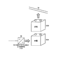
図4は、太陽光発電システムの第2実施形態を示す図である。第2実施形態の太陽光発電システムは、第1実施形態(図1、図2を参照)の構成要素に加えて、さらに、最終段の昇圧DC/DCコンバータ50から出力される直流電力(例えば±500kV)を蓄える複数台(図4では2台)の蓄電装置60A及び60Bを有する。
図4は、太陽光発電システムの第2実施形態を示す図である。第2実施形態の太陽光発電システムは、第1実施形態(図1、図2を参照)の構成要素に加えて、さらに、最終段の昇圧DC/DCコンバータ50から出力される直流電力(例えば±500kV)を蓄える複数台(図4では2台)の蓄電装置60A及び60Bを有する。
第1実施形態の太陽光発電システムでは、キャパシタの特性上、最終段の昇圧DC/DCコンバータ50の出力電圧が比較的短い時間で低下することが想定される。そのため、第1実施形態の太陽光発電システムでは、直流電力系統への出力電力を安定させることが困難な場合もあり得る。
そこで、第2実施形態の太陽光発電システムでは、電力バッファとして複数台の蓄電装置60A及び60Bを設置し、充電済みの蓄電装置から直流電力系統70への送電を行うように、蓄電装置60A及び60Bのローテーションを行う構成が採用されている。このような構成とすることにより、直流電力系統70への送電を安定化させることができる。
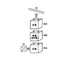
図5A~図5Cは、それぞれ、第2実施形態の一変形例(3台の蓄電装置60A~60Cを設置した場合)を示す図である。3台の蓄電装置60A~60Cは、少なくとも一つが最終段の昇圧DC/DCコンバータ50からの充電を行い、少なくとも別の一つが直流電力系統70への放電を行うように、各々の充放電状態がローテーションされる。
図5Aの第1ローテーション状態では、昇圧DC/DCコンバータ50の出力電力を用いて蓄電装置60Aを充電しつつ、前々回のローテーション状態(図5Bを参照)で満充電とされた蓄電装置60Cの出力電力を用いて直流電力系統70への送電が行われる。なお、前回のローテーション状態(図5Cを参照)で満充電とされた蓄電装置60Bは、次回のローテーション状態(図5Bを参照)での放電に備えて待機状態とされている。
蓄電装置60Cの放電が進むと、図5Bの第2ローテーション状態に移行される。この第2ローテーション状態では、昇圧DC/DCコンバータ50の出力電力を用いて蓄電装置60Cを充電しつつ、前々回のローテーション状態(図5Cを参照)で満充電状態とされた蓄電装置60Bの出力電力を用いて直流電力系統70への送電が行われる。なお、前回のローテーション状態(図5Aを参照)で満充電とされた蓄電装置60Aは、次回のローテーション状態(図5Cを参照)での放電に備えて待機状態とされている。
蓄電装置60Bの放電が進むと、図5Cの第3ローテーション状態に移行される。この第3ローテーション状態では、昇圧DC/DCコンバータ50の出力電力を用いて蓄電装置60Bを充電しつつ、前々回のローテーション状態(図5Aを参照)で満充電状態とされた蓄電装置60Aの出力電力を用いて直流電力系統70への送電が行われる。なお、前回のローテーション状態(図5Bを参照)で満充電とされた蓄電装置60Cは、次回のローテーション状態(図5Aを参照)での放電に備えて待機状態とされている。
蓄電装置60Aの放電が進むと、図5Aの第1ローテーション状態に移行され、その後も上記のローテーションが繰り返される。このような構成とすることにより、3台の蓄電装置60A~60Cのうち、少なくとも一つを昇圧DC/DCコンバータ50の出力電力によって充電しつつ、少なくとも別の一つから直流電力系統70への送電を行うことができるので、安定した送電を実現することが可能となる。
なお、夜間など、PVアレイ10での発電が停止したときでも、蓄電装置から直流電力系統70への送電を維持できるように、蓄電装置は3台以上設置されていることが望ましく、特に、送電安定性(特に電圧安定性)の観点から、急速充電かつ低速放電が可能な充放電特性を持つ蓄電装置を4台以上設置することが望ましい。なお、充電中の蓄電装置と送電中の蓄電装置以外は待機状態としておけばよい。待機状態の蓄電装置が満充電状態であるか放電済み状態(充電待ち状態)であるかは、太陽光発電システムの運用によって決定すればよい。
また、送電安定性を高めるためには、大規模容量のキャパシタやNAS電池など、できるだけ大容量の蓄電装置(理想的には1GW-500kV級の超大規模蓄電装置)を使用することが望ましい。
<第3実施形態>
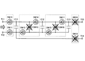
図6A及び図6Bは、それぞれ、スイッチトキャパシタ昇圧回路の一構成例(3倍昇圧型)を示す図である。なお、図6Aはキャパシタ充電時の様子を示しており、図6Bはキャパシタ放電時の様子を示している。本構成例のスイッチトキャパシタ昇圧回路は、キャパシタC11~C13と、半導体スイッチSW10~SW19と、を含む。
図6A及び図6Bは、それぞれ、スイッチトキャパシタ昇圧回路の一構成例(3倍昇圧型)を示す図である。なお、図6Aはキャパシタ充電時の様子を示しており、図6Bはキャパシタ放電時の様子を示している。本構成例のスイッチトキャパシタ昇圧回路は、キャパシタC11~C13と、半導体スイッチSW10~SW19と、を含む。
スイッチSW10は、第1入力端子T11とキャパシタC11の第1端との間を導通/遮断する。スイッチSW11は、第2入力端子T12とキャパシタC11の第2端との間を導通/遮断する。スイッチSW12は、キャパシタC11の第2端とキャパシタC12の第2端との間を導通/遮断する。スイッチSW13は、キャパシタC11の第1端とキャパシタC12の第2端との間を導通/遮断する。スイッチSW14は、キャパシタC11の第1端とキャパシタC12の第1端との間を導通/遮断する。スイッチSW15は、キャパシタC12の第2端とキャパシタC13の第2端との間を導通/遮断する。スイッチSW16は、キャパシタC12の第1端とキャパシタC13の第2端との間を導通/遮断する。スイッチSW17は、キャパシタC12の第1端とキャパシタC13の第1端との間を導通/遮断する。スイッチSW18は、キャパシタC13の第1端と第1出力端子T13との間を導通/遮断する。スイッチSW19は、キャパシタC11の第2端と第2出力端子T14との間を導通/遮断する。
図6Aの充電状態では、スイッチSW10~SW12、スイッチSW14、スイッチSW15、及び、スイッチSW17がオンとなり、スイッチSW13、スイッチSW16、スイッチSW18、及び、スイッチSW19がオフとなる。その結果、キャパシタC11~C13が第1入力端子T11と第2入力端子T12との間に並列接続された形となる。
図6Bの放電状態では、スイッチSW10~SW12、スイッチSW14、スイッチSW15、及び、スイッチSW17がオフとなり、スイッチSW13、スイッチSW16、スイッチSW18、及び、スイッチSW19がオンとなる。その結果、キャパシタC11~C13が第1出力端子T13と第2出力端子T14との間に直列接続された形となる。
図6A及び図6Bから分かるように、スイッチトキャパシタ昇圧回路は、その昇圧比が高くなるほど、必要なスイッチ素子の個数が増大する。また、スイッチトキャパシタ昇圧回路を形成するスイッチ素子には、高速なオン/オフ応答性が求められるので、パワートランジスタやサイリスタなどの半導体スイッチを用いることが必要となる。一方、半導体スイッチのオン抵抗は正の温度特性を持つことが知られている(図7を参照)。従って、スイッチ素子の個数増大(延いてはオン抵抗の増大)に伴う電力伝達効率の低下を回避するためには、半導体スイッチを冷却することが有効であると考えられる。
図8は、太陽光発電システムの第3実施形態を示す図である。第3構成例の太陽光発電システムは、先に説明したキャパシタ昇圧回路(31A、31B、41A、41B、51A、52B)や経路切替スイッチ(32、33、42、43、52、53)を各々構成する半導体スイッチを常時冷却する冷却装置80Aまたは80Bをさらに有する。
冷却装置としては、従来のサイリスタバルブに適用される水冷式の冷却装置ではなく、より強力に半導体スイッチを冷却することのできる冷却装置、例えば、電気的な冷凍装置80A(図8の左側)や、半導体スイッチを極低温の冷媒液(液体窒素など)に直接浸して冷却する冷却装置80B(図8の右側)を採用することが望ましい。なお、液体窒素を用いた冷却装置80Bは、簡素な構造で実現することができる上、既に半導体製造装置などへの適用もされていることから、太陽光発電システムへの導入に際して、技術的な課題はほとんどないと考えられる。ただし、冷媒液の種類については、液体窒素に限定されるものではない。
また、冷却装置80A及び80Bは、図8で示したように、半導体スイッチを一つずつ冷却する構成としてもよいし、図6A及び図6Bの破線で示したように、半導体スイッチを複数まとめて冷却する構成としてもよい。或いは、冷却装置80A及び80Bは、昇圧DC/DCコンバータ30~50を各々まとめて冷却する構成としてもよい。
このように、半導体スイッチを強烈に冷却する構成であれば、半導体スイッチのオン抵抗を低減して電力伝達効率を高めることができるので、多数の半導体スイッチを使用するスイッチトキャパシタ昇圧回路の変換効率向上(低電力損失)を実現することができる。例えば、交流の変圧にトランスを用いる場合には、トランスの前後にそれぞれ直交変換器と交直変換器を挿入する必要があり、ユニット全体の変換効率は95%以下となるが、第3実施形態の構成を採用すれば、上記ユニットに匹敵する効率(95%以上の効率)を期待することができる。
<その他の変形例>
なお、本発明の構成は、上記実施形態のほか、発明の主旨を逸脱しない範囲で種々の変更を加えることが可能である。
なお、本発明の構成は、上記実施形態のほか、発明の主旨を逸脱しない範囲で種々の変更を加えることが可能である。
本発明に係る直流昇圧装置は、例えば大規模な太陽光発電所(例えばギガワット級やメガワット級)の変電設備として利用することが可能である。また、本発明に係る直流昇圧装置は、家庭用の太陽光発電システムや小規模なスマートグリッドなど、その他の電力網にも広く適用することが可能である。また、本発明に係る直流昇圧装置は、太陽光発電システムの直流昇圧手段としてだけでなく、例えば、風力などの再生可能エネルギを用いた直流発電システム、回転機を用いた直流発電システム、或いは、燃料電池や蓄電池などを用いた直流電源システムの直流昇圧手段としても好適に用いることができる。また、本発明に係る直流昇圧装置は、電車や電気自動車などにも好適に搭載することが可能である。
10 太陽電池アレイ
10A 太陽電池パネル
10B 接続箱
10C 集電盤
20 電圧制御装置
30、40、50 昇圧DC/DCコンバータ
31A、31B、41A、41B、51A、51B スイッチトキャパシタ昇圧回路
32、42、52 入力側経路切替スイッチ
33、43、53 出力側経路切替スイッチ
60A、60B、60C 蓄電装置
70 直流電力系統
80A、80B 冷却装置
SW10~SW19 半導体スイッチ
C11、C12、C13 キャパシタ
T11、T12、T13、T14 端子
10A 太陽電池パネル
10B 接続箱
10C 集電盤
20 電圧制御装置
30、40、50 昇圧DC/DCコンバータ
31A、31B、41A、41B、51A、51B スイッチトキャパシタ昇圧回路
32、42、52 入力側経路切替スイッチ
33、43、53 出力側経路切替スイッチ
60A、60B、60C 蓄電装置
70 直流電力系統
80A、80B 冷却装置
SW10~SW19 半導体スイッチ
C11、C12、C13 キャパシタ
T11、T12、T13、T14 端子
Claims (19)
- 直流電源の出力を昇圧する少なくとも一段の昇圧DC/DCコンバータを有し、
前記昇圧DC/DCコンバータは、
キャパシタの充放電を利用して昇圧動作を行うトランスレスの第1キャパシタ昇圧回路及び第2キャパシタ昇圧回路と、
前記第1キャパシタ昇圧回路と前記第2キャパシタ昇圧回路の各入出力経路を切り替える経路切替スイッチと、
を含むことを特徴とする直流昇圧装置。 - 前記第1キャパシタ昇圧回路と前記第2キャパシタ昇圧回路は、それぞれ、複数のキャパシタを含み、各キャパシタを並列接続して充電する状態と、各キャパシタを直列接続して放電する状態と、を交互に繰り返すことにより、前段から供給される入力電圧を昇圧して後段に供給するスイッチトキャパシタ昇圧回路であることを特徴とする請求項1に記載の直流昇圧装置。
- 前記第1キャパシタ昇圧回路と前記第2キャパシタ昇圧回路は、互いの充放電状態が逆となるように制御されることを特徴とする請求項2に記載の直流昇圧装置。
- 前記経路切替スイッチは、前記第1キャパシタ昇圧回路と前記第2キャパシタ昇圧回路のうち、充電状態である方を前段と接続して後段から遮断する一方、放電状態である方を後段と接続して前段から遮断するように、前記第1キャパシタ昇圧回路と前記第2キャパシタ昇圧回路の各入出力経路を切り替えることを特徴とする請求項3に記載の直流昇圧装置。
- 前記経路切替スイッチは、リレーなどのアナログスイッチを用いて構成されていることを特徴とする請求項1~請求項4のいずれか一項に記載の直流昇圧装置。
- 前記経路切替スイッチは、パワートランジスタやサイリスタなどの半導体スイッチを用いて構成されていることを特徴とする請求項1~請求項4のいずれか一項に記載の直流昇圧装置。
- 前記昇圧DC/DCコンバータから出力される直流電力を蓄える複数の蓄電装置をさらに有することを特徴とする請求項1~請求項6のいずれか一項に記載の直流昇圧装置。
- 前記複数の蓄電装置は、少なくとも一つが前記昇圧DC/DCコンバータからの充電を行い、少なくとも別の一つが直流電力系統への放電を行うように、各々の充放電状態がローテーションされることを特徴とする請求項7に記載の直流昇圧装置。
- 前記第1キャパシタ昇圧回路及び前記第2キャパシタ昇圧回路、ないしは、前記経路切替スイッチを構成する半導体スイッチを冷却する冷却装置をさらに有することを特徴とする請求項1~請求項8のいずれか一項に記載の直流昇圧装置。
- 前記冷却装置は、電気的な冷凍装置であることを特徴とする請求項9に記載の直流昇圧装置。
- 前記冷却装置は、前記半導体スイッチを冷媒液に浸して冷却することを特徴とする請求項9に記載の直流昇圧装置。
- 前記冷却装置は、前記冷媒液として液体窒素を用いることを特徴とする請求項11に記載の直流昇圧装置。
- 前記冷却装置は、前記半導体スイッチを一つずつ冷却することを特徴とする請求項9~請求項12のいずれか一項に記載の直流昇圧装置。
- 前記冷却装置は、前記半導体スイッチを複数まとめて冷却することを特徴とする請求項9~請求項12のいずれか一項に記載の直流昇圧装置。
- 前記冷却装置は、前記昇圧DC/DCコンバータをまとめて冷却することを特徴とする請求項9~請求項12のいずれか一項に記載の直流昇圧装置。
- 前記昇圧DC/DCコンバータとして、
2kV~100Vの入力電圧を昇圧して30kV~3kVの出力電圧を生成する第1昇圧DC/DCコンバータと、
30kV~3kVの入力電圧を昇圧して250kV~60kVの出力電圧を生成する第2昇圧DC/DCコンバータと、
250kV~60kVの入力電圧を昇圧して±1000kV~±150kVの出力電圧を生成する第3昇圧DC/DCコンバータと、
を含むことを特徴とする請求項1~請求項15のいずれか一項に記載の直流昇圧装置。 - 太陽電池アレイと、
前記太陽電池アレイの出力を昇圧する請求項1~請求項16のいずれか一項に記載の直流昇圧装置と、
を有することを特徴とする太陽光発電システム。 - 電圧安定制御と最大電力点追従制御を行う電圧制御装置をさらに有することを特徴とする請求項17に記載の太陽光発電システム。
- 前記太陽電池アレイは、太陽電池パネルと、接続箱と、集電盤と、を含むことを特徴とする請求項17または請求項18に記載の太陽光発電システム。
Applications Claiming Priority (2)
| Application Number | Priority Date | Filing Date | Title |
|---|---|---|---|
| JP2011-113742 | 2011-05-20 | ||
| JP2011113742A JP5064584B1 (ja) | 2011-05-20 | 2011-05-20 | 直流昇圧装置及びこれを用いた太陽光発電システム |
Publications (1)
| Publication Number | Publication Date |
|---|---|
| WO2012160909A1 true WO2012160909A1 (ja) | 2012-11-29 |
Family
ID=47189623
Family Applications (1)
| Application Number | Title | Priority Date | Filing Date |
|---|---|---|---|
| PCT/JP2012/060365 Ceased WO2012160909A1 (ja) | 2011-05-20 | 2012-04-17 | 直流昇圧装置及びこれを用いた太陽光発電システム |
Country Status (2)
| Country | Link |
|---|---|
| JP (1) | JP5064584B1 (ja) |
| WO (1) | WO2012160909A1 (ja) |
Families Citing this family (4)
| Publication number | Priority date | Publication date | Assignee | Title |
|---|---|---|---|---|
| KR102396138B1 (ko) * | 2014-07-22 | 2022-05-10 | 셔랫, 리처드 | Dc 에너지 전달 장치, 애플리케이션, 부품 및 방법 |
| JP6411114B2 (ja) * | 2014-07-25 | 2018-10-24 | 日比谷総合設備株式会社 | 太陽光発電設備システム |
| US9800143B2 (en) | 2016-03-03 | 2017-10-24 | The Regents Of The University Of Michigan | Moving-sum charge pump |
| US10476382B2 (en) | 2016-03-03 | 2019-11-12 | The Regents Of The University Of Michigan | Energy harvester |
Citations (5)
| Publication number | Priority date | Publication date | Assignee | Title |
|---|---|---|---|---|
| JPS6192164A (ja) * | 1984-10-08 | 1986-05-10 | Sharp Corp | Dc/dcコンバ−タ |
| JPH01147877A (ja) * | 1987-12-04 | 1989-06-09 | Toshiba Corp | 電力変換装置 |
| JPH0240455A (ja) * | 1988-08-01 | 1990-02-09 | Daikin Ind Ltd | 潤滑油冷却装置 |
| JPH02146955A (ja) * | 1988-08-30 | 1990-06-06 | Michiko Naito | 静電トランス |
| JP2011015501A (ja) * | 2009-06-30 | 2011-01-20 | Panasonic Electric Works Co Ltd | 配電システム |
-
2011
- 2011-05-20 JP JP2011113742A patent/JP5064584B1/ja not_active Expired - Fee Related
-
2012
- 2012-04-17 WO PCT/JP2012/060365 patent/WO2012160909A1/ja not_active Ceased
Patent Citations (5)
| Publication number | Priority date | Publication date | Assignee | Title |
|---|---|---|---|---|
| JPS6192164A (ja) * | 1984-10-08 | 1986-05-10 | Sharp Corp | Dc/dcコンバ−タ |
| JPH01147877A (ja) * | 1987-12-04 | 1989-06-09 | Toshiba Corp | 電力変換装置 |
| JPH0240455A (ja) * | 1988-08-01 | 1990-02-09 | Daikin Ind Ltd | 潤滑油冷却装置 |
| JPH02146955A (ja) * | 1988-08-30 | 1990-06-06 | Michiko Naito | 静電トランス |
| JP2011015501A (ja) * | 2009-06-30 | 2011-01-20 | Panasonic Electric Works Co Ltd | 配電システム |
Also Published As
| Publication number | Publication date |
|---|---|
| JP5064584B1 (ja) | 2012-10-31 |
| JP2012244811A (ja) | 2012-12-10 |
Similar Documents
| Publication | Publication Date | Title |
|---|---|---|
| US12083913B2 (en) | Systems, apparatus and methods for electric vehicle charging via a power conversion system | |
| CN104137376B (zh) | 用于具有内部mvdc收集网的风电场的dc连接方案 | |
| EP2770624B1 (en) | Method and apparatus for producing three-phase current | |
| US9525284B2 (en) | Medium voltage DC collection system with power electronics | |
| De Doncker et al. | Power electronics for future utility applications | |
| CN204103503U (zh) | 一种基于中高压直流接入的光伏并网发电系统 | |
| US20130003423A1 (en) | Multi-input bidirectional dc-dc converter with high voltage conversion ratio | |
| WO2019213546A1 (en) | Systems and methods of dc power conversion and transmission for solar fields | |
| US9825470B2 (en) | Multi-source power converter | |
| Sano et al. | A boost conversion system consisting of multiple DC-DC converter modules for interfacing wind farms and HVDC transmission | |
| Chen et al. | A comparison of medium voltage high power DC/DC converters with high step-up conversion ratio for offshore wind energy systems | |
| Sheridan et al. | Assessment of DC/DC converters for use in DC nodes for offshore grids | |
| Naghizadeh et al. | A comprehensive review of power electronic converter topologies to integrate photovoltaics (PV), AC grid, and electric vehicles | |
| CN111030118B (zh) | 一种海岛输电系统及其控制方法 | |
| Manojkumar et al. | Power electronics interface for hybrid renewable energy system—A survey | |
| JP5064584B1 (ja) | 直流昇圧装置及びこれを用いた太陽光発電システム | |
| US10270368B2 (en) | Bi-directional, transformerless voltage system | |
| Sinenian et al. | Advances in power converters | |
| Sun et al. | Identifying opportunities for medium voltage DC systems in Australia | |
| CN102646995A (zh) | 基于电流源型逆变器的风、光、超导磁储能混合发电系统 | |
| Singh et al. | Sustainable cost-effective solution of climate emergency with many more societal benefits | |
| US20180083453A1 (en) | Power converting module, power generating system, and control method thereof | |
| Choi et al. | High gain DC/DC converter for the grid integration of large-scale PV systems | |
| Alhuwaishel et al. | A single stage transformer-less micro inverter with integrated battery storage system for residential applications | |
| CN105656321A (zh) | 一种直流母线两单元串联式的风电变流器主电路拓扑结构 |
Legal Events
| Date | Code | Title | Description |
|---|---|---|---|
| 121 | Ep: the epo has been informed by wipo that ep was designated in this application |
Ref document number: 12790334 Country of ref document: EP Kind code of ref document: A1 |
|
| NENP | Non-entry into the national phase |
Ref country code: DE |
|
| 122 | Ep: pct application non-entry in european phase |
Ref document number: 12790334 Country of ref document: EP Kind code of ref document: A1 |