WO2012153822A1 - シャッタ眼鏡、立体映像表示システム、および、シャッタ眼鏡の調整方法 - Google Patents
シャッタ眼鏡、立体映像表示システム、および、シャッタ眼鏡の調整方法 Download PDFInfo
- Publication number
- WO2012153822A1 WO2012153822A1 PCT/JP2012/062068 JP2012062068W WO2012153822A1 WO 2012153822 A1 WO2012153822 A1 WO 2012153822A1 JP 2012062068 W JP2012062068 W JP 2012062068W WO 2012153822 A1 WO2012153822 A1 WO 2012153822A1
- Authority
- WO
- WIPO (PCT)
- Prior art keywords
- shutter
- eye
- liquid crystal
- eye shutter
- transmittance
- Prior art date
- Legal status (The legal status is an assumption and is not a legal conclusion. Google has not performed a legal analysis and makes no representation as to the accuracy of the status listed.)
- Ceased
Links
Images




Classifications
-
- G—PHYSICS
- G09—EDUCATION; CRYPTOGRAPHY; DISPLAY; ADVERTISING; SEALS
- G09G—ARRANGEMENTS OR CIRCUITS FOR CONTROL OF INDICATING DEVICES USING STATIC MEANS TO PRESENT VARIABLE INFORMATION
- G09G3/00—Control arrangements or circuits, of interest only in connection with visual indicators other than cathode-ray tubes
- G09G3/001—Control arrangements or circuits, of interest only in connection with visual indicators other than cathode-ray tubes using specific devices not provided for in groups G09G3/02 - G09G3/36, e.g. using an intermediate record carrier such as a film slide; Projection systems; Display of non-alphanumerical information, solely or in combination with alphanumerical information, e.g. digital display on projected diapositive as background
- G09G3/003—Control arrangements or circuits, of interest only in connection with visual indicators other than cathode-ray tubes using specific devices not provided for in groups G09G3/02 - G09G3/36, e.g. using an intermediate record carrier such as a film slide; Projection systems; Display of non-alphanumerical information, solely or in combination with alphanumerical information, e.g. digital display on projected diapositive as background to produce spatial visual effects
-
- G—PHYSICS
- G09—EDUCATION; CRYPTOGRAPHY; DISPLAY; ADVERTISING; SEALS
- G09G—ARRANGEMENTS OR CIRCUITS FOR CONTROL OF INDICATING DEVICES USING STATIC MEANS TO PRESENT VARIABLE INFORMATION
- G09G3/00—Control arrangements or circuits, of interest only in connection with visual indicators other than cathode-ray tubes
- G09G3/20—Control arrangements or circuits, of interest only in connection with visual indicators other than cathode-ray tubes for presentation of an assembly of a number of characters, e.g. a page, by composing the assembly by combination of individual elements arranged in a matrix no fixed position being assigned to or needed to be assigned to the individual characters or partial characters
- G09G3/34—Control arrangements or circuits, of interest only in connection with visual indicators other than cathode-ray tubes for presentation of an assembly of a number of characters, e.g. a page, by composing the assembly by combination of individual elements arranged in a matrix no fixed position being assigned to or needed to be assigned to the individual characters or partial characters by control of light from an independent source
- G09G3/36—Control arrangements or circuits, of interest only in connection with visual indicators other than cathode-ray tubes for presentation of an assembly of a number of characters, e.g. a page, by composing the assembly by combination of individual elements arranged in a matrix no fixed position being assigned to or needed to be assigned to the individual characters or partial characters by control of light from an independent source using liquid crystals
- G09G3/3611—Control of matrices with row and column drivers
- G09G3/3648—Control of matrices with row and column drivers using an active matrix
-
- H—ELECTRICITY
- H04—ELECTRIC COMMUNICATION TECHNIQUE
- H04N—PICTORIAL COMMUNICATION, e.g. TELEVISION
- H04N13/00—Stereoscopic video systems; Multi-view video systems; Details thereof
- H04N13/10—Processing, recording or transmission of stereoscopic or multi-view image signals
- H04N13/106—Processing image signals
- H04N13/144—Processing image signals for flicker reduction
-
- H—ELECTRICITY
- H04—ELECTRIC COMMUNICATION TECHNIQUE
- H04N—PICTORIAL COMMUNICATION, e.g. TELEVISION
- H04N13/00—Stereoscopic video systems; Multi-view video systems; Details thereof
- H04N13/30—Image reproducers
- H04N13/332—Displays for viewing with the aid of special glasses or head-mounted displays [HMD]
- H04N13/341—Displays for viewing with the aid of special glasses or head-mounted displays [HMD] using temporal multiplexing
-
- H—ELECTRICITY
- H04—ELECTRIC COMMUNICATION TECHNIQUE
- H04N—PICTORIAL COMMUNICATION, e.g. TELEVISION
- H04N13/00—Stereoscopic video systems; Multi-view video systems; Details thereof
- H04N13/30—Image reproducers
- H04N13/398—Synchronisation thereof; Control thereof
Definitions
- the present invention relates to shutter glasses for observing stereoscopic display (3D display).
- LCDs consume less power than CRT (CathodeubeRay Tube) displays and are easy to miniaturize, so they are widely used in TVs, mobile phones, portable game consoles, in-vehicle navigation devices, etc. .
- CRT CathodeubeRay Tube
- stereoscopic display 3D display
- left-eye video and right-eye video are alternately displayed for each frame period in a time-sharing manner, and the user wears shutter glasses and observes the video so that the user can view a stereoscopic video.
- Patent Document 1 The shutter glasses have a left eye shutter and a right eye shutter that shield and open the left eye and the right eye, respectively.
- the shutter glasses deliver the left-eye video and the right-eye video to the left eye and right eye of the user, respectively, by synchronizing the operations of the left-eye shutter and right-eye shutter with the display of the liquid crystal display device.
- Patent Document 1 in order to prevent the crosstalk between the left and right images, the first left-eye frame L1 and the first left-eye frame L1 in the display period of the left-eye image are displayed. 2 sequentially displays the left-eye frame L2, and sequentially displays the first right-eye frame R1 and the second right-eye frame R2 of the same image as the first right-eye frame R1 during the right-eye video display period. ing.
- the shutter glasses of Patent Document 1 open the left-eye shutter only during a period in which the first left-eye frame L1 is rewritten to the second left-eye frame L2, and the first right-eye frame R1 is used for the second right-eye.
- the right-eye shutter is opened only during the period of rewriting to the frame R2.
- the shutter when the shutter is opened during a period in which the left-eye video is rewritten to the right-eye video (the period in which the first right-eye frame R1 is written), the left and right videos are mixed (the lower side of the screen is for the left eye). This is because the user sees the video image and the upper side is the video image for the right eye.
- JP 2010-117437 A (published May 27, 2010)
- the transmittance of the shutter glasses when the shutter is opened may be different between the left-eye shutter and the right-eye shutter due to manufacturing errors and the like.
- the liquid crystal shutter of the shutter glasses includes a first polarizing plate, a first glass plate, a liquid crystal layer, a second glass plate, and a second polarizing plate that are stacked in order.
- the transmittance changes when the shutter is opened.
- the first polarizing plate is attached to the first glass plate and the second polarizing plate is attached to the second glass plate.
- the transmittance of the manufactured shutter glasses when the shutter is opened is not necessarily the same on the left and right.
- the conventional configuration does not take into account the case where the left and right transmittances of the shutter glasses are different when the shutter is opened.
- the present invention has been made in view of the above problems, and an object of the present invention is to realize shutter glasses that make the amount of light entering the left and right eyes of the user comparable.
- the shutter glasses according to the present invention include a left-eye shutter and a right-eye shutter that perform an operation of switching between an open state that transmits incident light and a closed state that does not transmit incident light.
- a shutter driving unit that drives the left-eye shutter and the right-eye shutter under different driving conditions according to the difference between the transmittance characteristic of the left-eye shutter and the transmittance characteristic of the right-eye shutter. It is characterized by providing.
- the shutter driving unit performs the left-eye shutter and the right-eye shutter according to the difference between the transmittance characteristics of the left-eye shutter and the transmittance characteristics of the right-eye shutter. Drive under different driving conditions. Therefore, even when the transmittance characteristics of the shutters are different between the left and right, the user does not feel the difference between the left and right brightness by driving with driving conditions that consider the difference in the characteristics of the transmittance. Can reduce fatigue. Therefore, manufacturing tolerances can be increased and yield can be increased. Therefore, the manufacturing cost can be reduced.
- the shutter eyeglass adjustment method performs a left eye shutter and a right eye shutter that perform an operation of switching between an open state that transmits incident light and a closed state that does not transmit incident light. And measuring the intensity of light transmitted through the left-eye shutter and the right-eye shutter in the open state with respect to shutter glasses including a shutter drive unit that drives the left-eye shutter and the right-eye shutter.
- the transmittance characteristic of the left-eye shutter and the transmittance characteristic of the right-eye shutter are different, the transmittance characteristic of the left-eye shutter and the right-eye shutter Different driving conditions for the left-eye shutter and right-eye shutter are determined in accordance with the difference from the transmittance characteristic, and each driving condition is set in the shutter driving unit. Therefore, even when the transmittance characteristics of the shutters are different between the left and right, the user does not feel the difference between the left and right brightness by driving with driving conditions that consider the difference in the characteristics of the transmittance. It is possible to manufacture shutter glasses that can reduce fatigue.
- the shutter driving unit has the left-eye shutter and the right-eye shutter according to the difference between the transmittance characteristic of the left-eye shutter and the transmittance characteristic of the right-eye shutter.
- Each of the eye shutters is driven under different driving conditions.
- the user's fatigue can be reduced without making the user feel the difference between the left and right contrasts. Therefore, manufacturing tolerances can be increased and yield can be increased. Therefore, the manufacturing cost can be reduced.
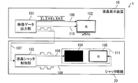
- FIG. 1 It is a figure which shows the structural example of the three-dimensional video display system which concerns on one Embodiment of this invention, and is a figure which shows the state which has closed the liquid-crystal shutter L (left). It is a figure which shows the structural example of the three-dimensional video display system which concerns on one Embodiment of this invention, and is a figure which shows the state which has closed liquid crystal shutter R (right). It is a block diagram which shows the functional structure of the shutter spectacles which concern on one Embodiment of this invention. It is a top view which shows the whole structure of a liquid crystal display device. It is an equivalent circuit diagram which shows one structure of the pixel which comprises the liquid crystal display panel. It is a top view which shows the structure of a pixel.
- shutter glasses used when observing stereoscopic image display by the shutter glasses method will be described.
- the shutter glasses-type stereoscopic image display technology is a left eye that alternately displays a left-eye image and a right-eye image for each frame period by time division, and closes and opens the left eye and the right eye, respectively.
- This is a technique for displaying a stereoscopic image to the user by wearing the shutter glasses having the shutter for the right eye and the shutter for the right eye.
- the stereoscopic image display system 1 includes a liquid crystal display device (display device) 10 and shutter glasses 20.
- the liquid crystal display device 10 includes a liquid crystal display panel 102 that alternately displays a left-eye image and a right-eye image for each frame period by time division.
- the user wears shutter glasses 20 having a left-eye shutter that closes and opens the left eye and a right-eye shutter that closes and opens the right eye, and observes the liquid crystal display panel 102, so that the user The video can be viewed.
- the liquid crystal display device 10 includes a video data output unit 101 and a liquid crystal display panel 102.
- the shutter glasses 20 include a liquid crystal shutter control unit 103 and a glasses unit 111.
- the eyeglass unit 111 includes a liquid crystal shutter L104 for the left eye and a liquid crystal shutter R105 for the right eye.
- the video data output unit 101 is a device that sends frame data 106 displayed as video from the liquid crystal display panel 102 to the liquid crystal display panel 102.
- the video data output unit 101 sequentially transmits left-eye video data and right-eye video data.
- the video data output unit 101 sends a backlight control signal 110 for controlling lighting of the backlight of the liquid crystal display panel 102 to the liquid crystal display panel 102.
- the video data output unit 101 sends a frame control signal 107 informing the frame status to the liquid crystal shutter control unit 103 of the shutter glasses 20 as an infrared signal.
- the frame control signal 107 is data for designating the opening / closing timing of the shutter.
- the liquid crystal display panel 102 displays the frame data 106 output from the video data output unit 101 as a video.
- the liquid crystal shutter control unit 103 controls OPEN / CLOSE of the liquid crystal shutter L104 and the liquid crystal shutter R105 according to the frame control signal 107.
- FIG. 1 shows a state in which the liquid crystal shutter R105 is OPEN (open) and the liquid crystal shutter L104 is CLOSE (closed).
- FIG. 2 shows a state in which the liquid crystal shutter L104 is OPEN (open) and the liquid crystal shutter R105 is CLOSE (closed).
- the liquid crystal shutter L104 of the glasses unit 111 is for use as a lens for the left eye of shutter glasses.
- the liquid crystal shutter L104 includes liquid crystal molecules therein, and opening / closing (transmission / non-transmission) of the shutter can be controlled by changing the alignment state of the liquid crystal molecules. That is, when the shutter state of the liquid crystal shutter L104 is OPEN, the display image of the liquid crystal display panel 102 can be seen by the user's left eye, but nothing can be seen when the shutter state is CLOSE.
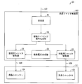
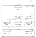
- FIG. 3 is a block diagram showing a functional configuration of the shutter glasses 20.
- the shutter glasses 20 include a liquid crystal shutter control unit (shutter driving unit) 103 and a glasses unit 111.
- the glasses unit 111 includes a liquid crystal shutter L104 and a liquid crystal shutter R105.
- the liquid crystal shutter control unit 103 includes a receiving unit 51, a driving timing signal generating unit 52, a driving voltage generating unit 53, a left eye shutter driving unit 54, and a right eye shutter driving unit 55.
- the liquid crystal shutter L104 and the liquid crystal shutter R105 of the shutter glasses 20 transmit incident light when no voltage is applied, and block incident light when a voltage is applied.
- the receiving unit 51 includes an infrared light receiving circuit that receives an infrared signal.
- the receiving unit 51 receives the frame control signal 107 output from the video data output unit 101 of the liquid crystal display device 10 and outputs the frame control signal 107 to the drive timing signal generating unit 52.
- the drive timing signal generation unit 52 Based on the frame control signal 107, the drive timing signal generation unit 52 generates a left eye drive timing signal indicating the timing for opening and closing the liquid crystal shutter L104 and a right eye drive timing signal indicating the timing for opening and closing the liquid crystal shutter R105. To do. For example, if the left-eye drive timing signal is L (Low), this indicates that the liquid crystal shutter L104 is opened. If the left-eye drive timing signal is H (High), the liquid crystal shutter L104 is closed. Indicates that The same applies to the right eye drive timing signal. The drive timing signal generation unit 52 transmits the liquid crystal shutter L104 when the voltage measured in advance (transmission state) is not applied and the transmission of the liquid crystal shutter R105 when the voltage is not applied (transmission state).
- the period during which the left and right liquid crystal shutters are open is set according to the ratio to the rate.
- the liquid crystal shutter L104 and the liquid crystal shutter R105 are alternately opened and closed. Details of the operation timing of each liquid crystal shutter will be described later.
- the drive timing signal generation unit 52 outputs the left eye drive timing signal to the left eye shutter drive unit 54 and outputs the right eye drive timing signal to the right eye shutter drive unit 55.
- the drive voltage generation unit 53 determines the voltage to be applied to the left and right liquid crystal shutters, and supplies the applied voltage to the left eye shutter drive unit 54 and the right eye shutter drive unit 55.
- the left-eye shutter drive unit 54 controls the liquid-crystal shutter L104 according to the left-eye drive timing signal received from the drive timing signal generation unit 52 and the applied voltage input from the drive voltage generation unit 53.
- the signal 108 is output.
- the left eye control signal 108 indicates a voltage applied to the liquid crystal shutter L104.
- the left-eye shutter drive unit 54 drives the liquid crystal shutter L104 to control opening / closing (transmission / non-transmission) of the liquid crystal shutter L104.
- the right-eye shutter drive unit 55 converts the right-eye drive timing signal received from the drive timing signal generation unit 52 and the applied voltage input from the drive voltage generation unit 53.
- the right eye control signal 109 is output to the liquid crystal shutter R105.
- the right-eye control signal 109 indicates a voltage applied to the liquid crystal shutter R105.
- the right-eye shutter drive unit 55 drives the liquid crystal shutter R105 to control opening / closing (transmission / non-transmission) of the liquid crystal shutter R105.
- the left-eye shutter drive unit 54 and the right-eye shutter drive unit 55 each liquid crystal shutter according to the difference in transmittance characteristics (transmittance when no voltage is applied (maximum transmittance)) between the left and right liquid crystal shutters.
- Different drive conditions refers to setting of the period of the open state and / or setting of the applied voltage in the open state. In the present embodiment, a case will be described in which the left and right liquid crystal shutters have different open periods.
- FIG. 4 is a plan view showing the overall configuration of the liquid crystal display device 10
- FIG. 5 is an equivalent circuit diagram showing one configuration of a pixel P (pixel portion) constituting the liquid crystal display panel 102.
- 6 is a plan view showing the configuration of the pixel P.
- the liquid crystal display device 10 includes an active matrix type liquid crystal display panel 102, a source line drive circuit 45s, a gate line drive circuit 45g, a storage capacitor line drive circuit 45c, a video data output unit 101, and a control.
- a circuit 45 is provided.
- the liquid crystal display panel 102 is configured by sandwiching a liquid crystal between an active matrix substrate and a counter substrate, and has a large number of pixels P arranged in a matrix.
- the liquid crystal display panel 102 includes a scanning gate line 11a, a collective charge gate line 11b, a collective discharge gate line 11c, and a source line 12 on an active matrix substrate.
- the transistor 31, the transistor 34, and the transistor 35, which are switching elements, the pixel electrode 30, and the storage capacitor line 16 (also referred to as CS wiring) are provided, and the counter electrode 14 is provided on the counter substrate.
- three types of gate wirings 11 a, 11 b, and 11 c are shown as one line, but each gate wiring is actually formed as a separate wiring (see FIGS. 5 and 6).
- the transistors 31, 34 and 35 are shown in FIGS. 5 and 6, but are omitted in FIG.
- the source wirings 12 (described as 12 (n) and 12 (n + 1) in FIG. 6) are formed one by one in the column direction (vertical direction) so as to be parallel to each other for each column of the pixels P.
- Scanning gate wirings 11a (indicated as 11a (n-1) and 11a (n) in FIG. 6) are formed one by one in the row direction (lateral direction) so as to be parallel to each other for each row of pixels P.
- the transistor 31 and the pixel electrode 30 are formed corresponding to each intersection of the source line 12 (12 (n)) and the scan gate line 11a (11a (n)). Further, the pixel electrode 30 forms a liquid crystal capacitor 32 through the liquid crystal between the counter electrode 14.
- One storage capacitor line 16 is formed in each row of the pixels P in the row direction (lateral direction) so as to be parallel to each other.
- the transistor 31 has a source electrode s connected to the source wiring 12 and a gate electrode g connected to the scanning gate wiring 11a.
- the drain electrode d of the transistor 31 is connected to the source electrode s of the transistor 34 and to one electrode 33 b of the storage capacitor 33.
- the transistor 34 has a source electrode s connected to the drain electrode d of the transistor 31 and a gate electrode g connected to the gate wiring 11b for batch charging.
- the drain electrode d of the transistor 34 is connected to the pixel electrode 30 and to the source electrode s of the transistor 35.
- the source electrode s is connected to the drain electrode d of the transistor 34, the gate electrode g is connected to the gate line 11c for collective discharge, and the drain electrode d is connected to the storage capacitor line 16.
- the pixel electrode 30 forms a liquid crystal capacitor (LC) 32 through a liquid crystal between the pixel electrode 30 and the counter electrode 14.
- the other electrode 33 a of the storage capacitor 33 is connected to the storage capacitor line 16.
- the storage capacitor 33 constituted by the electrode pairs 33 a and 33 b functions as a capacitor for charging in the pixel for temporarily charging the potential to be applied to the pixel electrode 30 before applying it to the pixel electrode 30.
- the gate of the transistor 31 is temporarily turned on by a gate signal (scanning signal) supplied to the scanning gate wiring 11a and the source signal (data signal) from the source wiring 12 is turned on.
- the held potential is once held in the holding capacitor 33.
- the pixel P is provided with a second transistor 35.
- a gate signal is supplied from the gate wiring 11c to the gate electrode g of the transistor 35 at such a timing that the transistors 35 of all the pixels in the liquid crystal display panel 102 are simultaneously turned on with the transistor 31 turned off. Thereby, each pixel electrode 30 in the liquid crystal display panel 102 can be discharged collectively. Therefore, the transistor 35 is called a collective discharge transistor, and the gate wiring 11c connected to the gate electrode g of the transistor 35 is called a collective discharge gate wiring.
- the pixel P is provided with a third transistor 34.
- the transistor 34 is turned on by a gate signal (control signal) supplied to the gate wiring 11 b and applies the potential held in the holding capacitor 33 to the pixel electrode 30. Accordingly, the pixel electrode 30 is set to a potential corresponding to the source signal, and a voltage corresponding to the source signal is applied to the liquid crystal interposed between the counter electrode 14 and the voltage corresponding to the source signal. Gray scale display can be realized.
- the gate wiring 11b supplies a gate signal to the gate electrode g of the transistor 34 at a timing such that the transistors 34 of all the pixels in the liquid crystal display panel 102 are simultaneously turned on with the transistors 31 and 35 turned off. Thereby, each pixel electrode 30 in the liquid crystal display panel 102 can be charged collectively. Therefore, the transistor 34 is called a collective charge transistor, and the gate wiring 11b connected to the gate electrode g of the transistor 34 is called a collective charge gate wiring.
- the liquid crystal display panel 102 configured as described above is driven by a source line drive circuit 45s, a gate line drive circuit 45g, a storage capacitor line drive circuit 45c, and a control circuit 45 for controlling them.
- the horizontal scanning period of each row is sequentially assigned, and each row is sequentially scanned.
- the gate wiring drive circuit 45g sequentially outputs a gate signal for turning on the transistor 31 to the scanning gate wiring 11a of the row in synchronization with the horizontal scanning period (1H) of each row.
- the gate wiring driving circuit 45g applies a gate signal for turning on the transistor 35 to each gate wiring 11c for collective discharge in order to discharge the pixel electrodes 30 of all the pixels P in the liquid crystal display panel 102 at once. Output.
- the gate wiring driving circuit 45g applies a gate signal for turning on the transistor 34 to each gate wiring 11b for batch charging in order to charge the pixel electrodes 30 of all the pixels P in the liquid crystal display panel 102 at once. Output.
- the source wiring drive circuit 45 s outputs a source signal to each source wiring 12.
- the video signal (frame data 106) supplied from the video data output unit 101 to the source wiring driving circuit 45s via the control circuit 45 is assigned to each column in the source wiring driving circuit 45s, and boosted or the like. Signal.
- the storage capacitor line drive circuit 45 c supplies a signal of a constant voltage to each storage capacitor line 16 and fixes the voltage of one electrode 33 a of the storage capacitor 33.
- the control circuit 45 controls the gate wiring driving circuit 45g, the source wiring driving circuit 45s, and the storage capacitor line driving circuit 45c described above based on the video signal (frame data 106) transmitted from the video data output unit 101. Thus, a gate signal, a source signal, and a CS signal are output from each of these circuits.
- the control circuit 45 also controls turning on / off of a backlight (not shown) based on the backlight control signal 110 transmitted from the video data output unit 101.
- an image based on the previous frame data of the current frame data is displayed on the liquid crystal display panel 102 (that is, the potential of the source signal based on the previous frame data in the liquid crystal capacitor 32 ((g in FIG. 7 In the pixel P, the plurality of gate wirings 11a are sequentially scanned by the gate signal (scanning signal) supplied to the scanning gate wiring 11a while the level A) is held in FIG. Is turned on (see (a) and (b) of FIG. 7).
- a potential corresponding to the source signal (data signal) from the source wiring 12 in the same horizontal scanning period (1H) this is called a data potential.
- FIG. 7E it is indicated by level b).
- the transistor 34 and the transistor 35 are in an off state.
- the data potential is held in the holding capacitor 33 of each pixel P by sequentially scanning the plurality of gate wirings 11a (n), 11a (n + 1).
- the transistor 35 is turned on by a gate signal supplied to the collective discharge gate wiring 11c while the transistor 34 is turned off (see FIG. 7D).
- the gate signal supplied to the gate line 11c for collective discharge is applied to the plurality of gate lines 11c at the same timing.
- the charges held in the liquid crystal capacitors 32 in all the pixels P of the liquid crystal display panel 102 are released to the holding capacitor lines 16, and the respective liquid crystal capacitors 32 are discharged together, as shown in FIG.
- the potential of the pixel electrode 30 is a common potential.
- the transistor 35 is turned off while the transistor 31 is turned off, and then the transistor 34 is turned on by a gate signal supplied to the gate wiring 11b for batch charge (see FIG. 7C).
- the gate signal supplied to the gate wiring 11b for batch charging is applied to the plurality of gate wirings 11b at the same timing.
- the charges held in the holding capacitors 33 in all the pixels P of the liquid crystal display panel 102 flow to the pixel electrodes 30, and the liquid crystal capacitors 32 are charged together.
- the potential of the pixel electrode 30 becomes a potential (eg, level B) based on the data potential (eg, level b).
- the liquid crystal capacitance 32 of each pixel can be charged and discharged in a unit of one frame (one vertical scanning period: 1 V). Therefore, even if the period during which the liquid crystal shutter L104 and the liquid crystal shutter R105 are opened is relatively long, it is possible to prevent the right-eye video and the left-eye video from being mixed. For example, in one vertical scanning period, the shutter can be opened during a period from when the liquid crystal capacitor 32 is collectively charged to when it is collectively discharged. Therefore, it is possible to suppress crosstalk and display a bright stereoscopic image without increasing the frame frequency.
- Vpx Q / C.
- Q is the total charge of the charge Q33 held in the holding capacitor 33 and the charge Q32 remaining in the pixel P.
- Cp is a parasitic capacitance with a bus line or the like. For this reason, in order to obtain a sufficient pixel voltage with respect to the voltage (data voltage) applied to the source s of the transistor 31, it is necessary to make C33 larger than C32.
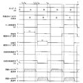
- FIG. 8 is a diagram showing the relationship between the frame data output to the liquid crystal display panel 102 and the timing of the control signal that controls the opening / closing of the shutter glasses 20.
- the horizontal axis indicates time.
- the video data output unit 101 outputs frame data 106 indicating video data to the liquid crystal display panel 102.
- the video data output unit 101 also sends a frame control signal 107 indicating the timing for switching between the right-eye video and the left-eye video to the shutter glasses 20 in units of one frame.
- the liquid crystal display panel 102 rewrites the display of each pixel to image data indicated by the input frame data at the end of the frame (one vertical scanning period) by collective discharge and collective charge (see FIG. 7). Therefore, the display of the liquid crystal display panel 102 is delayed by about one frame with respect to the frame data 106 input to the liquid crystal display panel 102.
- the video data output unit 101 transmits an infrared pulse signal indicating that the frame control signal 107 is H.
- the reception unit 51 of the liquid crystal shutter control unit 103 outputs the H-level frame control signal 107 to the drive timing signal generation unit 52 while receiving the infrared pulse signal indicating that the frame control signal 107 is H. .
- the video data output unit 101 does not transmit an infrared pulse signal when the frame control signal 107 is L.
- the reception unit 51 of the liquid crystal shutter control unit 103 outputs an L-level frame control signal 107 to the drive timing signal generation unit 52 while the infrared pulse signal is not received.
- the video data output unit 101 may transmit an infrared pulse signal indicating that the frame control signal 107 is L.
- the reception unit 51 outputs the L-level frame control signal 107 to the drive timing signal generation unit 52 while receiving the infrared pulse signal indicating that the frame control signal 107 is L.
- the display on the liquid crystal display panel 102 is rewritten from the right-eye image to the left-eye image by collective discharge and collective charge.
- frame control signal 107 is at the H level.
- the drive timing signal generation unit 52 outputs an H level left eye drive timing signal to the left eye shutter drive unit 54, and outputs an H level right eye drive timing signal to the right eye shutter drive unit 55. Output.
- the left-eye shutter drive unit 54 and the right-eye shutter drive unit 55 output the voltage V1 supplied from the drive voltage generation unit 53 to the respective liquid crystal shutters. .
- the liquid crystal shutter to which the voltage V1 is applied is in a non-transmissive state that does not transmit light.
- the left-eye shutter drive unit 54 and the right-eye shutter drive unit 55 output a voltage 0 (V) to the respective liquid crystal shutters when the drive timing signal is at the L level.
- the liquid crystal shutter to which no voltage is applied is in a transmissive state that transmits light.
- both the left and right liquid crystal shutters are in an opaque state.
- the frame control signal 107 is switched from the H level to the L level.
- the drive timing signal generation unit 52 switches the left-eye drive timing signal output to the left-eye shutter drive unit 54 from H to L. If the left-eye drive timing signal is L, the left-eye shutter drive unit 54 outputs a voltage 0 as the left-eye control signal 108 to the liquid crystal shutter L104. That is, no voltage is applied to the liquid crystal shutter L104. Therefore, the liquid crystal shutter L104 is in a transmissive state (open state). However, the transmittance of the liquid crystal shutter L104 increases continuously as shown in FIG. 8 according to the reaction speed of the liquid crystal. After a while, the transmittance of the liquid crystal shutter L104 reaches the maximum value Tl.
- the drive timing signal generation unit 52 changes the left-eye drive timing signal from L to H at time t3 after a preset period tl has elapsed from time t2 when the left-eye drive timing signal was switched from H to L. Switch. Therefore, the left-eye shutter drive unit 54 outputs the voltage V1 to the liquid crystal shutter L104 as the left-eye control signal 108. As a result, the liquid crystal shutter L104 enters a non-transmissive state (closed state). Note that the transmittance of the liquid crystal shutter L104 continuously decreases according to the reaction speed of the liquid crystal as shown in FIG. After a while, the transmittance of the liquid crystal shutter L104 becomes zero.
- period tl is set so that the liquid crystal shutter L104 is in a non-transmissive state by time t4 when the image displayed on the liquid crystal display panel 102 switches from the left eye to the right eye.
- the display on the liquid crystal display panel 102 is rewritten from the left-eye image to the right-eye image by collective discharge and collective charge.
- the frame control signal 107 is switched from the L level to the H level.
- the drive timing signal generation unit 52 switches the right-eye drive timing signal output to the right-eye shutter drive unit 55 from H to L. Therefore, the right-eye shutter drive unit 55 outputs a voltage 0 as the right-eye control signal 109 to the liquid crystal shutter R105. That is, no voltage is applied to the liquid crystal shutter R105. Therefore, the liquid crystal shutter R105 is in a transmissive state (open state).
- the transmittance of the liquid crystal shutter R105 continuously increases as shown in FIG. After a while, the transmittance of the liquid crystal shutter R105 reaches the maximum value Tr.
- the drive timing signal generation unit 52 changes the right-eye drive timing signal from L to H at time t6 after a preset period tr has elapsed from time t5 when the right-eye drive timing signal was switched from H to L. Switch. Therefore, the right-eye shutter drive unit 55 outputs the voltage V1 as the right-eye control signal 109 to the liquid crystal shutter R105. As a result, the liquid crystal shutter R105 enters a non-transmissive state (closed state). Note that the transmittance of the liquid crystal shutter R105 continuously decreases as shown in FIG. 8 according to the reaction speed of the liquid crystal. After a while, the transmittance of the liquid crystal shutter R105 becomes zero.
- the liquid crystal shutter control unit 103 repeats the above operation in accordance with the frame control signal 107.
- the maximum value Tr of the transmittance of the liquid crystal shutter R105 is larger than the maximum value Tl of the transmittance of the liquid crystal shutter L104. Therefore, the amount of transmitted light per unit time in the transmissive state is larger in the liquid crystal shutter R105 than in the liquid crystal shutter L104. Therefore, in the drive timing signal generation unit 52, the period tr for opening the liquid crystal shutter R105 is set shorter than the period tl for opening the liquid crystal shutter L104.
- a value obtained by integrating the transmittance with the time of the open state is proportional to the amount of transmitted light per frame of each liquid crystal shutter.
- FIG. 9 is a flowchart illustrating a process of adjusting the amount of light transmitted through the left and right liquid crystal shutters of the shutter glasses.
- the transmittance of the liquid crystal shutter L104 in a state where no voltage is applied (transmission state) and the transmittance of the liquid crystal shutter R105 may differ due to manufacturing errors or the like.
- a light source and a light intensity measuring device are prepared, and the intensity of light transmitted through the liquid crystal shutter L104 or the liquid crystal shutter R105 in an open state where no voltage is applied is measured by the light intensity measuring device (S1).
- the maximum transmittance Tl of the liquid crystal shutter L104 and the maximum transmittance Tr of the liquid crystal shutter R105 are specified (S2).
- the liquid crystal shutter correction drive condition is obtained according to the ratio between the maximum transmittance Tl of the liquid crystal shutter L104 and the maximum transmittance Tr of the liquid crystal shutter R105 (S3).
- the correction drive condition means, for example, a period tl for opening the liquid crystal shutter L104 and a period tr for opening the liquid crystal shutter R105.
- the correction drive conditions obtained in S3 (that is, the period tl for opening the liquid crystal shutter L104 and the period tr for opening the liquid crystal shutter R105) are written in the drive timing signal generation unit 52 of the shutter glasses 20 (S4).
- said adjustment process can be automatically performed by the adjustment apparatus provided with a light source, a light intensity measuring device, a correction drive condition writing apparatus, etc.
- a period (driving condition) in which each liquid crystal shutter is opened in each frame is set according to the difference in transmittance characteristics between the left and right liquid crystal shutters (maximum transmittance ratio), and the same on the left and right.
- the amount of transmitted light per frame is adjusted to be the same. Therefore, even if there is a difference in transmittance between the left and right liquid crystal shutters of the shutter glasses, the difference in brightness between the images viewed through the left and right liquid crystal shutters can be reduced. Therefore, the user's fatigue can be reduced without making the user feel the difference between the left and right contrasts. Therefore, manufacturing tolerances can be increased and yield can be increased. Therefore, the manufacturing cost can be reduced.
- the shutter glasses 20 can be used for a display device that rewrites each pixel for each row without performing collective discharge and collective charge.
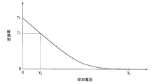
- FIG. 10 is a graph showing the relationship between the applied voltage and the transmittance in the liquid crystal shutter R105.
- the transmittance of the liquid crystal shutter R105 becomes the maximum value Tr.
- the transmittance decreases as the applied voltage increases, and the transmittance becomes 0 at the applied voltage V1.
- the transmittance of the liquid crystal shutter L104 when the applied voltage is 0 is Tl smaller than Tr.
- the transmittance can be set to Tl.
- the drive timing signal generation unit 52 sets the open state period tl of the liquid crystal shutter L104 and the open state period tr of the liquid crystal shutter R105 to be the same.
- the drive voltage generation unit 53 determines the voltage (V1) to be applied to the liquid crystal shutter L104 and the liquid crystal shutter R105 in the closed state, and uses the left eye shutter drive unit 54 and the right eye as an H level (closed) voltage. This is supplied to the shutter drive unit 55. Further, the drive voltage generation unit 53 determines a voltage (0) to be applied to the liquid crystal shutter L104 in the open state, and supplies it to the left-eye shutter drive unit 54 as an L level (open) voltage. The drive voltage generation unit 53 determines the voltage (V2) to be applied to the liquid crystal shutter R105 in the open state, and supplies the voltage (V2) to the right-eye shutter drive unit 55 as an L level (open) voltage. Here, 0 ⁇ V2 ⁇ V1.
- FIG. 11 is a diagram showing the relationship between the frame data output to the liquid crystal display panel 102 and the timing of the control signal for controlling the opening / closing of the shutter glasses 20.
- the horizontal axis indicates time.
- the relationship between the frame data 106, the display on the liquid crystal display panel 102, and the frame control signal 107 is the same as in the first embodiment (FIG. 8).
- the display on the liquid crystal display panel 102 is rewritten from the right-eye image to the left-eye image by batch discharge and batch charge.
- the frame control signal 107 is at the H level.
- the drive timing signal generation unit 52 outputs an H level left eye drive timing signal to the left eye shutter drive unit 54, and outputs an H level right eye drive timing signal to the right eye shutter drive unit 55. Output.
- the left eye shutter drive unit 54 and the right eye shutter drive unit 55 apply the H level voltage V1 supplied from the drive voltage generation unit 53 to the respective liquid crystal shutters. Output to.
- the liquid crystal shutter to which the voltage V1 is applied is in a non-transmissive state that does not transmit light.
- the left eye shutter drive unit 54 outputs the L level voltage 0 supplied from the drive voltage generation unit 53 to the liquid crystal shutter L104.
- the right eye shutter drive unit 55 outputs the L level voltage V2 supplied from the drive voltage generation unit 53 to the liquid crystal shutter R105.
- the liquid crystal shutter to which no voltage is applied and the liquid crystal shutter to which the voltage V2 is applied are in a transmissive state that transmits light.
- both the left and right liquid crystal shutters are in an opaque state.
- the frame control signal 107 is switched from the H level to the L level.
- the drive timing signal generation unit 52 switches the left-eye drive timing signal output to the left-eye shutter drive unit 54 from H to L. If the left-eye drive timing signal is L, the left-eye shutter drive unit 54 outputs a voltage 0 as the left-eye control signal 108 to the liquid crystal shutter L104. That is, no voltage is applied to the liquid crystal shutter L104. Therefore, the liquid crystal shutter L104 is in a transmissive state (open state). However, the transmittance of the liquid crystal shutter L104 increases continuously as shown in FIG. 11 according to the reaction speed of the liquid crystal. After a while, the transmittance of the liquid crystal shutter L104 reaches the maximum value Tl.
- the drive timing signal generation unit 52 changes the left-eye drive timing signal from L to H at time t13 after a preset period tl has elapsed from time t12 when the left-eye drive timing signal was switched from H to L. Switch. Therefore, the left-eye shutter drive unit 54 outputs the voltage V1 to the liquid crystal shutter L104 as the left-eye control signal 108. As a result, the liquid crystal shutter L104 enters a non-transmissive state (closed state). Note that the transmittance of the liquid crystal shutter L104 continuously decreases according to the reaction speed of the liquid crystal as shown in FIG. After a while, the transmittance of the liquid crystal shutter L104 becomes zero.
- period tl is set so that the liquid crystal shutter L104 is in a non-transmissive state by time t14 when the image displayed on the liquid crystal display panel 102 switches from the left eye to the right eye.
- the display on the liquid crystal display panel 102 is rewritten from the left-eye image to the right-eye image by batch discharge and batch charge.
- the frame control signal 107 is switched from the L level to the H level.
- the drive timing signal generation unit 52 switches the right-eye drive timing signal output to the right-eye shutter drive unit 55 from H to L. Therefore, the right-eye shutter drive unit 55 outputs the L-level voltage V2 as the right-eye control signal 109 to the liquid crystal shutter R105. Therefore, the liquid crystal shutter R105 is in a transmissive state (open state).
- the transmittance of the liquid crystal shutter R105 continuously increases as shown in FIG. After a while, the transmittance of the liquid crystal shutter R105 becomes Tr '.
- Tr ′ Tl.
- the drive timing signal generation unit 52 changes the right eye drive timing signal from L to H at time t16 after a preset period tr has elapsed from time t15 when the right eye drive timing signal was switched from H to L. Switch.
- tr tl. Therefore, the right-eye shutter drive unit 55 outputs the voltage V1 as the right-eye control signal 109 to the liquid crystal shutter R105.
- the liquid crystal shutter R105 enters a non-transmissive state (closed state). Note that the transmittance of the liquid crystal shutter R105 continuously decreases according to the liquid crystal reaction speed as shown in FIG. After a while, the transmittance of the liquid crystal shutter R105 becomes zero.
- the liquid crystal shutter control unit 103 repeats the above operation in accordance with the frame control signal 107.
- the transmittance of the left and right liquid crystal shutters in the open state is measured in advance, and the voltage supplied to each of the left-eye shutter drive unit 54 and the right-eye shutter drive unit 55 according to the ratio of the transmittance is determined as a drive voltage generation unit. 53 may be set.
- the applied voltage in the open state with respect to the liquid crystal shutter R105 having a high original transmittance is adjusted so that the transmittance in the open state is the same in the liquid crystal shutter L104 and the liquid crystal shutter R105.
- the transmittance in the open state of the liquid crystal shutter R105 is made the same as the transmittance in the open state of the liquid crystal shutter L104. Therefore, when the same image is viewed on the left and right, the transmitted light amount per frame is the same on the left and right.
- the liquid crystal shutter that transmits light in a state where no voltage is applied (normal white) is described.
- a liquid crystal shutter that transmits light according to the applied voltage normally black
- the transmittance can be adjusted. That is, in the case of normal black, the transmittance in the open state is made the same by applying an opening voltage smaller than that of the other liquid crystal shutter to the liquid crystal shutter having a large original transmittance (maximum transmittance). Can do.
- the present embodiment is a combination of the first embodiment and the second embodiment.
- the shutter glasses 20 of the present embodiment have different open period periods for the left and right liquid crystal shutters, and the applied voltage in the open state is different. Adjust the transmittance by making it different. When the applied voltage is 0, it is assumed that the transmittance Tl of the liquid crystal shutter L104 is smaller than the transmittance Tr of the liquid crystal shutter R105.
- the drive timing signal generation unit 52 makes the open state period tl of the liquid crystal shutter L104 different from the open state period tr of the liquid crystal shutter R105.
- the drive voltage generation unit 53 determines the voltage (V1) to be applied to the liquid crystal shutter L104 and the liquid crystal shutter R105 in the closed state, and uses the left eye shutter drive unit 54 and the right eye as an H level (closed) voltage. This is supplied to the shutter drive unit 55. Further, the drive voltage generation unit 53 determines a voltage (0) to be applied to the liquid crystal shutter L104 in the open state, and supplies it to the left-eye shutter drive unit 54 as an L level (open) voltage. The drive voltage generation unit 53 determines a voltage (V3) to be applied to the liquid crystal shutter R105 in the open state, and supplies the voltage (V3) to the right-eye shutter drive unit 55 as an L level (open) voltage. Here, 0 ⁇ V3 ⁇ V1.
- FIG. 12 is a diagram showing the relationship between the frame data output to the liquid crystal display panel 102 and the timing of the control signal that controls the opening / closing of the shutter glasses 20.
- the horizontal axis indicates time.
- the relationship between the frame data 106, the display on the liquid crystal display panel 102, and the frame control signal 107 is the same as in the first embodiment (FIG. 8).
- the display on the liquid crystal display panel 102 is rewritten from the right-eye image to the left-eye image by collective discharge and collective charge.
- the frame control signal 107 is at the H level.
- the drive timing signal generation unit 52 outputs an H level left eye drive timing signal to the left eye shutter drive unit 54, and outputs an H level right eye drive timing signal to the right eye shutter drive unit 55. Output.
- the left eye shutter drive unit 54 and the right eye shutter drive unit 55 apply the H level voltage V1 supplied from the drive voltage generation unit 53 to the respective liquid crystal shutters. Output to.
- the liquid crystal shutter to which the voltage V1 is applied is in a non-transmissive state that does not transmit light.
- the left eye shutter drive unit 54 outputs the L level voltage 0 supplied from the drive voltage generation unit 53 to the liquid crystal shutter L104.
- the right-eye shutter drive unit 55 outputs the L-level voltage V3 supplied from the drive voltage generation unit 53 to the liquid crystal shutter R105.
- the liquid crystal shutter to which no voltage is applied and the liquid crystal shutter to which the voltage V3 is applied are in a transmissive state that transmits light.
- both the left and right liquid crystal shutters are in an opaque state.
- the frame control signal 107 is switched from the H level to the L level.
- the drive timing signal generation unit 52 switches the left-eye drive timing signal output to the left-eye shutter drive unit 54 from H to L. If the left-eye drive timing signal is L, the left-eye shutter drive unit 54 outputs a voltage 0 as the left-eye control signal 108 to the liquid crystal shutter L104. That is, no voltage is applied to the liquid crystal shutter L104. Therefore, the liquid crystal shutter L104 is in a transmissive state (open state). However, the transmittance of the liquid crystal shutter L104 increases continuously as shown in FIG. 12 according to the reaction speed of the liquid crystal. After a while, the transmittance of the liquid crystal shutter L104 reaches the maximum value Tl.
- the drive timing signal generation unit 52 changes the left-eye drive timing signal from L to H at time t23 after a preset period tl has elapsed since time t22 when the left-eye drive timing signal was switched from H to L. Switch. Therefore, the left-eye shutter drive unit 54 outputs the voltage V1 to the liquid crystal shutter L104 as the left-eye control signal 108. As a result, the liquid crystal shutter L104 enters a non-transmissive state (closed state). Note that the transmittance of the liquid crystal shutter L104 continuously decreases according to the reaction speed of the liquid crystal as shown in FIG. After a while, the transmittance of the liquid crystal shutter L104 becomes zero.
- period tl is set so that the liquid crystal shutter L104 is in a non-transparent state by time t24 when the image displayed on the liquid crystal display panel 102 is switched from the left eye to the right eye.
- the display on the liquid crystal display panel 102 is rewritten from the left-eye image to the right-eye image by collective discharge and collective charge.
- the frame control signal 107 is switched from the L level to the H level.
- the drive timing signal generation unit 52 switches the right-eye drive timing signal output to the right-eye shutter drive unit 55 from H to L. Therefore, the right-eye shutter drive unit 55 outputs the L-level voltage V3 as the right-eye control signal 109 to the liquid crystal shutter R105. Therefore, the liquid crystal shutter R105 is in a transmissive state (open state).
- the transmittance of the liquid crystal shutter R105 continuously increases as shown in FIG. After a while, the transmittance of the liquid crystal shutter R105 becomes Tr ′′.
- the drive timing signal generation unit 52 changes the right eye drive timing signal from L to H at time t26 after a preset period tr has elapsed from time t25 when the right eye drive timing signal was switched from H to L. Switch.
- tr ⁇ tl. Therefore, the right-eye shutter drive unit 55 outputs the voltage V1 as the right-eye control signal 109 to the liquid crystal shutter R105.
- the liquid crystal shutter R105 enters a non-transmissive state (closed state). Note that the transmittance of the liquid crystal shutter R105 continuously decreases according to the reaction speed of the liquid crystal as shown in FIG. After a while, the transmittance of the liquid crystal shutter R105 becomes zero.
- the liquid crystal shutter control unit 103 repeats the above operation in accordance with the frame control signal 107.
- the period of the liquid crystal shutter in the open state and the applied voltage in the open state are adjusted so that the value obtained by integrating the transmittance with the time in the open state is the same on the left and right.
- the product Tl ⁇ tl of the transmittance of the liquid crystal shutter L104 and the open state period and the product Tr ′′ ⁇ tr of the transmittance of the liquid crystal shutter R105 and the open state period are the same.
- the transmittance of the liquid crystal shutter R105 and the period of the open state are set. Therefore, when the same image is viewed on the left and right, the transmitted light amount per frame is the same on the left and right.
- the shutter glasses can be adjusted in the same manner as in the first or second embodiment.
- FIG. 13 is a block diagram showing a functional configuration of the shutter glasses 21 of the present embodiment.
- the shutter glasses 21 include a liquid crystal shutter control unit (shutter driving unit) 112 and a glasses unit 111.
- the glasses unit 111 includes a liquid crystal shutter L104 and a liquid crystal shutter R105.
- the liquid crystal shutter control unit 112 includes a reception unit 51, a drive timing signal generation unit 52, a drive voltage generation unit 53, a left eye shutter drive unit 54, a right eye shutter drive unit 55, and a setting input unit (instruction input unit) 56. Is provided.
- the setting input unit 56 stores a period tl for opening the liquid crystal shutter L104 and a period tr for opening the liquid crystal shutter R105 in each frame.
- the setting input unit 56 includes input devices such as “+” and “ ⁇ ” buttons, and receives user inputs (instructions).
- the setting input unit 56 changes a period during which the left and right liquid crystal shutters are opened according to a user input. For example, when the user presses the “ ⁇ ” button, the period tl for opening the liquid crystal shutter L104 is changed to be longer, and the period tr for opening the liquid crystal shutter R105 is changed to be shorter.
- the setting input unit 56 writes the changed settings of the periods tl and tr into the drive timing signal generation unit 52. As a result, the amount of light transmitted through the liquid crystal shutter L104 per frame increases, and the amount of light transmitted through the liquid crystal shutter R105 decreases.
- the “+” button the period tl for opening the liquid crystal shutter L104 is changed short, and the period tr for opening the liquid crystal shutter R105 is changed long. As a result, the amount of light transmitted through the liquid crystal shutter L104 per frame is reduced, and the amount of light transmitted through the liquid crystal shutter R105 is increased.
- the setting input unit 56 may change the setting of the voltage that the drive voltage generation unit 53 supplies to the left-eye shutter drive unit 54 and the right-eye shutter drive unit 55 in accordance with a user input. That is, the voltage applied to the left and right liquid crystal shutters may be changed in accordance with a user instruction.
- the receiving unit 51 of the shutter glasses 21 may be configured to accept an input of a transmitted light amount change instruction from a remote controller.
- the setting input unit 56 receives the transmitted light amount change instruction from the receiving unit 51, adjusts the open state period in accordance with the change instruction, and sets the changed open state period in the drive timing signal generation unit 52. Write.
- Shutter glasses include a left-eye shutter and a right-eye shutter that perform an operation of switching between an open state that transmits incident light and a closed state that does not transmit incident light.
- a shutter drive unit that drives the left-eye shutter and the right-eye shutter under different driving conditions according to the difference between the transmittance characteristic and the transmittance characteristic of the right-eye shutter.
- the shutter driving unit performs the left-eye shutter and the right-eye shutter according to the difference between the transmittance characteristics of the left-eye shutter and the transmittance characteristics of the right-eye shutter. Drive under different driving conditions. Therefore, even when the transmittance characteristics of the shutters are different between the left and right, the user does not feel the difference between the left and right brightness by driving with driving conditions that consider the difference in the characteristics of the transmittance. Can reduce fatigue. Therefore, manufacturing tolerances can be increased and yield can be increased. Therefore, the manufacturing cost can be reduced.
- the shutter driving unit may change the left-eye shutter and the right-eye shutter under different driving conditions according to a ratio of the maximum transmittance of the left-eye shutter and the maximum transmittance of the right-eye shutter. It may be driven.
- the shutter driving unit drives the left-eye shutter and the right-eye shutter differently according to the ratio between the maximum transmittance of the left-eye shutter and the maximum transmittance of the right-eye shutter. Drive under conditions. Therefore, even if the transmissivity characteristics (maximum transmissivity) of each shutter are different between the left and right, the user feels the difference between the left and right brightness by driving under the driving conditions that take into account the ratio of the maximum transmissivity. The user's fatigue can be reduced.
- the shutter driving unit differs between the left-eye shutter and the right-eye shutter so that the transmitted light amount of the left-eye shutter and the transmitted light amount of the right-eye shutter are the same for the same incident light. You may drive on driving conditions.
- the amount of transmitted light on the left and right in each frame is approximately the same. Therefore, the user's fatigue can be reduced without making the user feel the difference between the left and right contrasts.
- the shutter driving unit may make the length of the open state period different between the left-eye shutter and the right-eye shutter.
- the shutter driving unit includes the left-eye shutter and the left-eye shutter so that a value obtained by integrating the transmittance in the open state in the open-state period is the same between the left-eye shutter and the right-eye shutter.
- the right eye shutter may be driven.
- the amount of transmitted light in the open state period is proportional to the value obtained by integrating the transmittance in the open period. According to the above configuration, each shutter is driven so that the value obtained by integrating the transmittance in the open state in the open state period is the same between the left and right shutters. Therefore, the amount of light transmitted through the left and right shutters can be made approximately the same.
- the transmittance of the left eye shutter and the right eye shutter changes according to the applied voltage
- the shutter driving unit is configured to apply the applied voltage of the left eye shutter in the open state to the left eye shutter.
- the configuration may be such that the applied voltage of the right-eye shutter in the open state is different.
- the transmittance ratio in the open state of the left and right shutters can be adjusted by changing the applied voltage of each shutter. Therefore, the amount of light transmitted through the left and right shutters can be made approximately the same.
- the shutter driving unit may be configured such that the transmittance of the left eye shutter in the open state and the transmittance of the right eye shutter in the open state are the same. Different applied voltages may be applied to the shutters for use.
- the applied voltage in the open state is adjusted to adjust the applied voltage in the open state.
- the transmittance of the left-eye shutter and the transmittance of the right-eye shutter in the open state can be made the same.
- the left-eye shutter and the right-eye shutter may be constituted by liquid crystal shutters.
- the open state and the closed state can be switched by applying a voltage to the liquid crystal shutter, and the open state of the left and right liquid crystal shutters can be adjusted by adjusting the applied voltage of the left and right liquid crystal shutters. It is possible to adjust the ratio of transmittance.
- the shutter glasses may be configured to include an instruction input unit that receives an instruction to change the driving condition from a user and changes the driving condition of the shutter driving unit in accordance with the user's instruction.
- the left and right shutter drive conditions can be changed in accordance with a user instruction. Therefore, even when the transmissivity of the left and right shutters has changed due to deterioration over time or the like, the driving conditions of the left and right shutters can be changed so that the user does not feel the difference between the left and right brightness.
- a stereoscopic video display system includes the shutter glasses and a display device that displays a left-eye image and a right-eye image by time division.
- a method for adjusting shutter glasses includes a left-eye shutter and a right-eye shutter that perform an operation of switching between an open state that transmits incident light and a closed state that does not transmit incident light, and the left-eye shutter.
- the transmittance characteristic of the left-eye shutter and the transmittance characteristic of the right-eye shutter are different, the transmittance characteristic of the left-eye shutter and the right-eye shutter Different driving conditions for the left-eye shutter and right-eye shutter are determined in accordance with the difference from the transmittance characteristic, and each driving condition is set in the shutter driving unit. Therefore, even when the transmittance characteristics of the shutters are different between the left and right, the user does not feel the difference between the left and right brightness by driving with driving conditions that consider the difference in the characteristics of the transmittance. It is possible to manufacture shutter glasses that can reduce fatigue.
- the present invention can be used for shutter glasses for observing stereoscopic display (3D display).
- Liquid crystal display device (display device) 11a (scanning) gate wiring 11b (collective charging) gate wiring 11c (collective discharging) gate wiring 12 source wiring 14 counter electrode 16 holding capacitance line 20, 21 shutter glasses 30 pixel electrode 31 transistor 32 liquid crystal capacitance 33 Holding capacity 34 Collective charge transistor 35 Collective discharge transistor 51 Receiver 52 Drive timing signal generator 53 Drive voltage generator 54 Left-eye shutter driver (shutter driver) 55 Shutter drive unit for right eye (shutter drive unit) 56 Setting input section (instruction input section) 101 Video data output unit 102 Liquid crystal display panels 103 and 112 Liquid crystal shutter control unit (shutter driving unit) 104 Liquid crystal shutter L 105 Liquid crystal shutter R 106 Frame data 107 Frame control signal 108 Left eye control signal 109 Right eye control signal 111 Eyeglass part P Pixel
Landscapes
- Engineering & Computer Science (AREA)
- Multimedia (AREA)
- Signal Processing (AREA)
- Physics & Mathematics (AREA)
- Computer Hardware Design (AREA)
- General Physics & Mathematics (AREA)
- Theoretical Computer Science (AREA)
- Chemical & Material Sciences (AREA)
- Crystallography & Structural Chemistry (AREA)
- Testing, Inspecting, Measuring Of Stereoscopic Televisions And Televisions (AREA)
Abstract
本発明の一態様に係るシャッタ眼鏡(20)は、入射光を透過させる開状態と入射光を透過させない閉状態とを切り替える動作を行う液晶シャッタL(104)および液晶シャッタR(105)を備え、液晶シャッタL(104)の透過率の特性と液晶シャッタR(105)の透過率の特性との違いに応じて、液晶シャッタL(104)および液晶シャッタR(105)を異なる駆動条件で駆動するシャッタ駆動部(54・55)を備える。
Description
本発明は、立体表示(3D表示)を観察するためのシャッタ眼鏡に関する。
近年、フラットパネルディスプレイとして、液晶ディスプレイ等の需要が急速に伸びている。液晶ディスプレイは、CRT(Cathode Ray Tube)ディスプレイに比べて、消費電力が少なく、小型化がしやすいため、テレビを始め、携帯電話、携帯型ゲーム機、車載用ナビゲーション装置等に幅広く利用されている。
ところで、昨今、各種表示装置において、立体表示(3D表示)を可能とする映像表示技術が提案されている。例えば、液晶表示装置において、左眼用映像と右眼用映像とを時分割によりフレーム期間毎に交互に表示し、ユーザが、シャッタ眼鏡を着用して映像を観察することにより、ユーザに立体映像を視認させる技術が提案されている(特許文献1)。シャッタ眼鏡は、左眼および右眼をそれぞれ遮蔽および開放する左眼用シャッタおよび右眼用シャッタを有する。シャッタ眼鏡は、左眼用シャッタおよび右眼用シャッタの動作を液晶表示装置の表示と同期させることにより、ユーザの左眼および右眼に、それぞれ左眼用映像および右眼用映像を届ける。
なお、特許文献1の構成では、左右の映像のクロストークを防止するために、左眼用映像の表示期間において第1左眼用フレームL1と、第1左眼用フレームL1と同じ映像の第2左眼用フレームL2を順次表示し、右眼用映像の表示期間において第1右眼用フレームR1と、第1右眼用フレームR1と同じ映像の第2右眼用フレームR2を順次表示している。そして、特許文献1のシャッタ眼鏡は、第1左眼用フレームL1を第2左眼用フレームL2に書き換える期間のみ左眼用シャッタを開放し、第1右眼用フレームR1を第2右眼用フレームR2に書き換える期間のみ右眼用シャッタを開放する。これは、例えば、左眼用映像を右眼用映像に書き換える期間(第1右眼用フレームR1を書き込む期間)にシャッタを開放すると、左右の映像が混在した状態(画面の下側が左眼用映像、上側が右眼用映像である状態)を視認してしまうためである。
ここで、製造時の誤差等に起因して、シャッタ眼鏡のシャッタ開放時における透過率は、左眼用シャッタおよび右眼用シャッタで異なることがある。例えば、シャッタ眼鏡の液晶シャッタは、第1偏光板と、第1ガラス板と、液晶層と、第2ガラス板と、第2偏光板とが順に重なって構成される。この液晶層を挟む2枚のガラス板の間隔が変化すると(液晶層の厚みが変化すると)、シャッタ開放時における透過率が変化する。また、第1偏光板は第1ガラス板に、第2偏光板は第2ガラス板に貼り付けられるが、第1偏光板の偏光方向と第2偏光板の偏光方向との角度が変化すると、シャッタ開放時における透過率が変化する。そのため、製造されたシャッタ眼鏡のシャッタ開放時における透過率は、左右で必ずしも同じではない。
しかしながら、上記従来の構成では、シャッタ開放時におけるシャッタ眼鏡の左右の透過率が異なる場合について、考慮されていない。
特許文献1に記載の構成では、右眼用シャッタも左眼用シャッタも所定の期間同様に開放するので、シャッタ眼鏡の左右の透過率が異なる場合、ユーザの眼に入る光量が左右で異なることになる。左眼用および右眼用の画像の輝度が異なると、3D映像の観察によってユーザの疲労が増大してしまう。
シャッタ開放時における透過率が均一であるシャッタ眼鏡を製造するためには、製造時の公差を小さくして管理する必要がある。しかしながら、製造時の公差を小さくすると歩留まりが悪くなり、製造コストが増大する。また、上記公差を満たさない製品は不良品として廃棄しなければならず、製造コストが増大する。
本発明は、上記の問題点に鑑みてなされたものであり、その目的は、ユーザの左右の眼に入る光量を同程度にするシャッタ眼鏡を実現することにある。
本発明に係るシャッタ眼鏡は、入射光を透過させる開状態と入射光を透過させない閉状態とを切り替える動作を行う左眼用シャッタおよび右眼用シャッタを備え、上記の課題を解決するために、上記左眼用シャッタの透過率の特性と上記右眼用シャッタの透過率の特性との違いに応じて、上記左眼用シャッタおよび上記右眼用シャッタを異なる駆動条件で駆動するシャッタ駆動部を備えることを特徴としている。
上記の構成によれば、シャッタ駆動部が、左眼用シャッタの透過率の特性と右眼用シャッタの透過率の特性との違いに応じて、左眼用シャッタおよび右眼用シャッタのそれぞれを異なる駆動条件で駆動する。よって、各シャッタの透過率の特性が左右で異なる場合であっても、その透過率の特性の違いを考慮した駆動条件で駆動することにより、ユーザに左右の明暗の差を感じさせず、ユーザの疲労を軽減することができる。またそれゆえ、製造における公差を大きくすることができ、歩留まりを高くすることができる。よって、製造コストを低減することができる。
本発明に係るシャッタ眼鏡の調整方法は、上記の課題を解決するために、入射光を透過させる開状態と入射光を透過させない閉状態とを切り替える動作を行う左眼用シャッタおよび右眼用シャッタと、上記左眼用シャッタおよび上記右眼用シャッタを駆動するシャッタ駆動部を備えるシャッタ眼鏡について、上記開状態における上記左眼用シャッタおよび上記右眼用シャッタを透過した光の強度をそれぞれ測定するステップと、上記測定された光の強度に基づいて、上記左眼用シャッタの透過率の特性と上記右眼用シャッタの透過率の特性とを特定するステップと、上記左眼用シャッタの透過率の特性と上記右眼用シャッタの透過率の特性との違いに応じて、互いに異なる上記左眼用シャッタの駆動条件および上記右眼用シャッタの駆動条件を決定するステップと、上記シャッタ駆動部に、上記各駆動条件を設定するステップとを含むことを特徴としている。
上記の構成によれば、左眼用シャッタの透過率の特性と右眼用シャッタの透過率の特性とが異なる場合であっても、左眼用シャッタの透過率の特性と右眼用シャッタの透過率の特性との違いに応じて、互いに異なる左眼用シャッタの駆動条件および右眼用シャッタの駆動条件を決定し、シャッタ駆動部に各駆動条件を設定する。よって、各シャッタの透過率の特性が左右で異なる場合であっても、その透過率の特性の違いを考慮した駆動条件で駆動することにより、ユーザに左右の明暗の差を感じさせず、ユーザの疲労を軽減することができるシャッタ眼鏡を製造することができる。
以上のように、本発明に係るシャッタ眼鏡は、シャッタ駆動部が、左眼用シャッタの透過率の特性と右眼用シャッタの透過率の特性との違いに応じて、左眼用シャッタおよび右眼用シャッタのそれぞれを異なる駆動条件で駆動する。
よって、ユーザに左右の明暗の差を感じさせず、ユーザの疲労を軽減することができる。またそれゆえ、製造における公差を大きくすることができ、歩留まりを高くすることができる。よって、製造コストを低減することができる。
[実施形態1]
以下、本発明の一実施形態について、図1~図9に基づいて説明する。
以下、本発明の一実施形態について、図1~図9に基づいて説明する。
本実施形態では、シャッタ眼鏡方式による立体映像表示を観察する際に用いるシャッタ眼鏡について、説明する。ここで、シャッタ眼鏡方式の立体映像表示技術とは、左眼用映像と右眼用映像とを時分割によりフレーム期間毎に交互に表示し、左眼および右眼をそれぞれ閉鎖および開放する左眼用シャッタおよび右眼用シャッタを有するシャッタ眼鏡をユーザが着用することにより、ユーザに立体映像を表示する技術のことである。
(立体映像表示システムの構成)
図1および図2は、本実施形態に係る立体映像表示システム1の構成例を示す図であり、それぞれ液晶シャッタL(左)、液晶シャッタR(右)を閉鎖している状態を示す図である。本実施形態の立体映像表示システム1は、液晶表示装置(表示装置)10とシャッタ眼鏡20とで構成されている。液晶表示装置10は、左眼用映像と右眼用映像とを時分割によりフレーム期間毎に交互に表示する液晶表示パネル102を有している。ユーザは、左眼を閉鎖および開放する左眼用シャッタと、右眼を閉鎖および開放する右眼用シャッタとを有するシャッタ眼鏡20を着用して液晶表示パネル102を観察することにより、ユーザは立体映像を視認することができる。
図1および図2は、本実施形態に係る立体映像表示システム1の構成例を示す図であり、それぞれ液晶シャッタL(左)、液晶シャッタR(右)を閉鎖している状態を示す図である。本実施形態の立体映像表示システム1は、液晶表示装置(表示装置)10とシャッタ眼鏡20とで構成されている。液晶表示装置10は、左眼用映像と右眼用映像とを時分割によりフレーム期間毎に交互に表示する液晶表示パネル102を有している。ユーザは、左眼を閉鎖および開放する左眼用シャッタと、右眼を閉鎖および開放する右眼用シャッタとを有するシャッタ眼鏡20を着用して液晶表示パネル102を観察することにより、ユーザは立体映像を視認することができる。
図1および図2に示すように、液晶表示装置10は、映像データ出力部101と、液晶表示パネル102とを備える。シャッタ眼鏡20は、液晶シャッタ制御部103と、眼鏡部111とを備える。眼鏡部111は、左眼用の液晶シャッタL104および右眼用の液晶シャッタR105を有している。
映像データ出力部101は、液晶表示パネル102から映像として表示されるフレームデータ106を、液晶表示パネル102に送出する装置である。本実施形態では、映像データ出力部101は、左眼用の映像データ、右眼用の映像データを順番に送出する。さらに、映像データ出力部101は、液晶表示パネル102のバックライトの点灯を制御するバックライト制御信号110を液晶表示パネル102に送出する。また、映像データ出力部101は、フレームのステータスを知らせるフレーム制御信号107を、シャッタ眼鏡20の液晶シャッタ制御部103に対して赤外線信号として送出する。フレーム制御信号107は、シャッタの開閉のタイミングを指定するためのデータである。
液晶表示パネル102は、映像データ出力部101より出力されたフレームデータ106を映像として表示する。
液晶シャッタ制御部103は、フレーム制御信号107に応じて、液晶シャッタL104および液晶シャッタR105のOPEN/CLOSE(開閉)を制御する。図1は、液晶シャッタR105がOPEN(開)であり、液晶シャッタL104がCLOSE(閉)である状態を示している。一方、図2は、液晶シャッタL104がOPEN(開)であり、液晶シャッタR105がCLOSE(閉)である状態を示している。
眼鏡部111の液晶シャッタL104は、シャッタ眼鏡の左眼用のレンズとして使用されるためのものである。この液晶シャッタL104には、内部に液晶分子が含まれており、この液晶分子の配向状態を変更することによって、シャッタの開閉(透過/不透過)を制御することができる。すなわち、液晶シャッタL104のシャッタ状態がOPENのときには、ユーザの左眼には、液晶表示パネル102の表示映像が見えるが、シャッタ状態がCLOSEのときには何も見えないようになっている。
(シャッタ眼鏡の構成)
次に、シャッタ眼鏡20のより詳細な構成について、図3を参照しながら説明する。
次に、シャッタ眼鏡20のより詳細な構成について、図3を参照しながら説明する。
図3は、シャッタ眼鏡20の機能的構成を示すブロック図である。シャッタ眼鏡20は、液晶シャッタ制御部(シャッタ駆動部)103および眼鏡部111を備える。眼鏡部111は、液晶シャッタL104および液晶シャッタR105を有している。液晶シャッタ制御部103は、受信部51、駆動タイミング信号生成部52、駆動電圧生成部53、左眼用シャッタ駆動部54、および右眼用シャッタ駆動部55を備える。
シャッタ眼鏡20の液晶シャッタL104および液晶シャッタR105は、電圧が印加されていない場合に入射する光を透過させ、電圧が印加されている場合に入射する光を遮断する。
受信部51は、赤外線信号を受信する赤外線受光回路を含む。受信部51は、液晶表示装置10の映像データ出力部101から出力されたフレーム制御信号107を受信し、フレーム制御信号107を駆動タイミング信号生成部52に出力する。
駆動タイミング信号生成部52は、フレーム制御信号107に基づき、液晶シャッタL104を開閉するタイミングを示す左眼用駆動タイミング信号と、液晶シャッタR105を開閉するタイミングを示す右眼用駆動タイミング信号とを生成する。例えば、左眼用駆動タイミング信号がL(Low)であれば、液晶シャッタL104を開状態にすることを示し、左眼用駆動タイミング信号がH(High)であれば、液晶シャッタL104を閉状態にすることを示す。右眼用駆動タイミング信号についても同様である。駆動タイミング信号生成部52は、あらかじめ測定された電圧を印加していないときの(透過状態の)液晶シャッタL104の透過率と電圧を印加していないときの(透過状態の)液晶シャッタR105の透過率との比に応じて、左右それぞれの液晶シャッタが開いている期間を設定する。本実施の形態では、液晶シャッタL104および液晶シャッタR105は、交互に開閉される。各液晶シャッタの動作タイミングの詳細は後述する。
駆動タイミング信号生成部52は、左眼用駆動タイミング信号を左眼用シャッタ駆動部54に出力し、右眼用駆動タイミング信号を右眼用シャッタ駆動部55に出力する。
駆動電圧生成部53は、左右それぞれの液晶シャッタに印加する電圧を決定し、印加電圧を左眼用シャッタ駆動部54および右眼用シャッタ駆動部55に供給する。
左眼用シャッタ駆動部54は、駆動タイミング信号生成部52から受け取った左眼用駆動タイミング信号と、駆動電圧生成部53から入力される印加電圧とに応じて、液晶シャッタL104に左眼用制御信号108を出力する。左眼用制御信号108は、液晶シャッタL104に印加する電圧を示す。これにより、左眼用シャッタ駆動部54は、液晶シャッタL104を駆動し、液晶シャッタL104の開閉(透過/不透過)を制御する。
右眼用シャッタ駆動部55は、左眼用シャッタ駆動部54と同様に、駆動タイミング信号生成部52から受け取った右眼用駆動タイミング信号と、駆動電圧生成部53から入力される印加電圧とに応じて、液晶シャッタR105に右眼用制御信号109を出力する。右眼用制御信号109は、液晶シャッタR105に印加する電圧を示す。これにより、右眼用シャッタ駆動部55は、液晶シャッタR105を駆動し、液晶シャッタR105の開閉(透過/不透過)を制御する。
左眼用シャッタ駆動部54および右眼用シャッタ駆動部55は、左右の液晶シャッタの透過率の特性(電圧を印加しないときの透過率(最大透過率))の違いに応じて、各液晶シャッタの駆動条件を異ならせる。ここで、駆動条件とは、開状態の期間の設定、および/または、開状態における印加電圧の設定を指す。本実施形態では、左右の液晶シャッタについて開状態の期間を異ならせる場合について説明する。
(液晶表示装置の構成)
ここで、液晶表示装置10およびその内部に備えられた液晶表示パネル102のより具体的な構成について、図4、図5、および図6を参照しながら説明する。図4は、液晶表示装置10の全体構成を示す平面図であり、図5は、液晶表示パネル102を構成している画素P(画素部)の一つの構成を示す等価回路図であり、図6は、画素Pの構成を示す平面図である。
ここで、液晶表示装置10およびその内部に備えられた液晶表示パネル102のより具体的な構成について、図4、図5、および図6を参照しながら説明する。図4は、液晶表示装置10の全体構成を示す平面図であり、図5は、液晶表示パネル102を構成している画素P(画素部)の一つの構成を示す等価回路図であり、図6は、画素Pの構成を示す平面図である。
図4に示すように、液晶表示装置10は、アクティブマトリクス型の液晶表示パネル102、ソース配線駆動回路45s、ゲート配線駆動回路45g、保持容量線駆動回路45c、映像データ出力部101、および、コントロール回路45を備えている。
液晶表示パネル102は、アクティブマトリクス基板と対向基板との間に液晶を挟持して構成されており、マトリクス状に配列された多数の画素Pを有している。
そして、図5および図6に示すように、液晶表示パネル102は、アクティブマトリクス基板上に、スキャン用のゲート配線11a、一括充電用のゲート配線11b、一括放電用のゲート配線11c、ソース配線12、スイッチング素子であるトランジスタ31・トランジスタ34・トランジスタ35、画素電極30、および保持容量線16(CS配線とも呼ぶ)を備え、対向基板上に対向電極14を備えている。なお、図4では、3種類のゲート配線11a・11b・11cを一本で示しているが、実際は、それぞれのゲート配線が別個の配線で形成されている(図5および図6参照)。また、トランジスタ31・34・35は、図5および図6では図示しているが、図4では省略している。
ソース配線12(図6では、12(n)、12(n+1)と記載)は、画素Pの各列について、互いに平行となるように列方向(縦方向)に1本ずつ形成されている。スキャン用のゲート配線11a(図6では、11a(n-1)、11a(n)と記載)は、画素Pの各行について、互いに平行となるように行方向(横方向)に1本ずつ形成されている。トランジスタ31および画素電極30は、ソース配線12(12(n))とスキャン用のゲート配線11a(11a(n))との各交点に対応してそれぞれ形成されている。また、画素電極30は、対向電極14との間に液晶を介して液晶容量32を形成している。保持容量線16は、画素Pの各行について、互いに平行となるように行方向(横方向)に1本ずつ形成されている。
(画素Pの具体的な構成)
続いて、一画素Pのより具体的な構成について、図5および図6を参照しながら説明する。図5および図6に示すように、画素P内には、3つのトランジスタ31・34・35と、液晶容量32を形成するための画素電極30および対向電極14と、保持容量33を形成するための保持容量電極対33a・33bとが設けられている。
続いて、一画素Pのより具体的な構成について、図5および図6を参照しながら説明する。図5および図6に示すように、画素P内には、3つのトランジスタ31・34・35と、液晶容量32を形成するための画素電極30および対向電極14と、保持容量33を形成するための保持容量電極対33a・33bとが設けられている。
トランジスタ31は、そのソース電極sがソース配線12に、ゲート電極gがスキャン用のゲート配線11aにそれぞれ接続されている。また、トランジスタ31のドレイン電極dは、トランジスタ34のソース電極sに接続されているとともに、保持容量33の一方の電極33bに接続されている。
トランジスタ34は、そのソース電極sがトランジスタ31のドレイン電極dに、ゲート電極gが一括充電用のゲート配線11bにそれぞれ接続されている。また、トランジスタ34のドレイン電極dは、画素電極30に接続されているとともに、トランジスタ35のソース電極sに接続されている。
トランジスタ35は、そのソース電極sがトランジスタ34のドレイン電極dに、ゲート電極gが一括放電用のゲート配線11cに、ドレイン電極dが保持容量線16にそれぞれ接続されている。
また、画素電極30は、対向電極14との間に液晶を介して液晶容量(LC)32を形成している。さらに、保持容量33の他方の電極33aは、保持容量線16に接続されている。電極対33a・33bで構成される保持容量33は、画素電極30に印加すべき電位を、画素電極30に印加する前に一旦充電しておくための画素内充電用のキャパシタとして機能する。
上記のような構成を有する画素Pでは、スキャン用のゲート配線11aに供給されるゲート信号(走査信号)によってトランジスタ31のゲートを一旦オンし、ソース配線12からのソース信号(データ信号)に応じた電位を、一旦保持容量33に保持する。
また、画素Pには2つ目のトランジスタ35が設けられている。このトランジスタ35のゲート電極gには、トランジスタ31をオフにした状態で、液晶表示パネル102内の全画素のトランジスタ35が同時にオンするようなタイミングでゲート配線11cからゲート信号が供給される。これにより、液晶表示パネル102内の各画素電極30を一括して放電することができる。そのため、トランジスタ35を一括放電用トランジスタと呼び、また、トランジスタ35のゲート電極gに接続されたゲート配線11cを一括放電用のゲート配線と呼ぶ。
さらに、画素Pには3つ目のトランジスタ34が設けられている。このトランジスタ34は、ゲート配線11bに供給されるゲート信号(制御信号)によってオンとなり、保持容量33に保持された電位を画素電極30に印加する。これにより、画素電極30を上記ソース信号に応じた電位に設定し、対向電極14との間に介在する液晶に対して上記ソース信号に応じた電圧を印加することによって、上記ソース信号に応じた階調表示を実現することができる。
なお、ゲート配線11bは、トランジスタ31・35をオフにした状態で、液晶表示パネル102内の全画素のトランジスタ34が同時にオンするようなタイミングでトランジスタ34のゲート電極gにゲート信号を供給する。これにより、液晶表示パネル102内の各画素電極30を一括して充電することができる。そのため、トランジスタ34を、一括充電用トランジスタと呼び、また、トランジスタ34のゲート電極gに接続されたゲート配線11bを一括充電用のゲート配線と呼ぶ。
なお、画素Pにおける各トランジスタ31・34・35のオン/オフの動作タイミングについては、後述する。
(液晶表示装置10内の各種回路)
上記構成の液晶表示パネル102は、ソース配線駆動回路45s、ゲート配線駆動回路45g、保持容量線駆動回路45c、およびこれらを制御するコントロール回路45によって駆動される。
上記構成の液晶表示パネル102は、ソース配線駆動回路45s、ゲート配線駆動回路45g、保持容量線駆動回路45c、およびこれらを制御するコントロール回路45によって駆動される。
本実施形態では、周期的に繰り返される垂直走査期間におけるアクティブ期間(有効走査期間)において、各行の水平走査期間を順次割り当て、各行を順次走査していく。
そのために、ゲート配線駆動回路45gは、トランジスタ31をオンするためのゲート信号を各行の水平走査期間(1H)に同期して当該行のスキャン用のゲート配線11aに対して順次出力する。
また、ゲート配線駆動回路45gは、液晶表示パネル102内の全画素Pの画素電極30を一括して放電するために、トランジスタ35をオンするためのゲート信号を一括放電用の各ゲート配線11cに対して出力する。
さらに、ゲート配線駆動回路45gは、液晶表示パネル102内の全画素Pの画素電極30を一括して充電するために、トランジスタ34をオンするためのゲート信号を一括充電用の各ゲート配線11bに対して出力する。
また、ソース配線駆動回路45sは、各ソース配線12に対してソース信号を出力する。このソース信号は、映像データ出力部101からコントロール回路45を介してソース配線駆動回路45sに供給された映像信号(フレームデータ106)を、ソース配線駆動回路45sにおいて各列に割り当て、昇圧等を施した信号である。
また、保持容量線駆動回路45cは、各保持容量線16に一定の電圧の信号を供給し、保持容量33の一方の電極33aの電圧を固定する。
コントロール回路45は、映像データ出力部101から送信された映像信号(フレームデータ106)に基づいて、上述したゲート配線駆動回路45g、ソース配線駆動回路45s、および保持容量線駆動回路45cを制御することにより、これら各回路から、ゲート信号、ソース信号、およびCS信号を出力させるものである。また、コントロール回路は45は、映像データ出力部101から送信されたバックライト制御信号110に基づいて、バックライト(図示せず)の点灯および消灯の制御も行う。
(画素P内の各トランジスタの動作タイミング)
以下には、上記のような画像表示面内における液晶容量32の一括充電および一括放電を実現するための各トランジスタ31・34・35の動作タイミングについて、図5および図7のタイミングチャートを参照しながら説明する。
以下には、上記のような画像表示面内における液晶容量32の一括充電および一括放電を実現するための各トランジスタ31・34・35の動作タイミングについて、図5および図7のタイミングチャートを参照しながら説明する。
まず、現フレームデータの一つ前のフレームデータに基づく画像が液晶表示パネル102に表示されている(すなわち、液晶容量32に一つ前のフレームデータに基づくソース信号の電位(図7の(g)においてレベルA)が保持されている)間に、画素Pでは、スキャン用のゲート配線11aに供給されるゲート信号(走査信号)によって、複数のゲート配線11aを順次走査してトランジスタ31のゲートをオンする(図7の(a)および(b)参照)。これにより、同じ水平走査期間(1H)におけるソース配線12からのソース信号(データ信号)に応じた電位(これをデータ電位と呼ぶ。また、図7の(e)ではレベルbで示す)を、一旦保持容量33に保持する(図7の(f)参照)。このとき、トランジスタ34およびトランジスタ35は、オフの状態になっている。
上記のように、複数のゲート配線11a(n)、11a(n+1)・・・を順次走査して行くことで、各画素Pの保持容量33にデータ電位が保持される。
続いて、トランジスタ31をオフした後、トランジスタ34をオフ状態のまま、一括放電用のゲート配線11cに供給されるゲート信号によってトランジスタ35をオンする(図7の(d)参照)。ここで、一括放電用のゲート配線11cに供給されるゲート信号は、複数のゲート配線11cに対して同じタイミングで印加される。これにより、液晶表示パネル102の全画素P内の液晶容量32に保持されていた電荷は保持容量線16へ逃がされ、各液晶容量32は一括して放電され、図7の(g)に示すように画素電極30の電位はコモン電位となる。
次に、トランジスタ31をオフ状態のまま、トランジスタ35をオフし、その後一括充電用のゲート配線11bに供給されるゲート信号によってトランジスタ34をオンする(図7の(c)参照)。ここで、一括充電用のゲート配線11bに供給されるゲート信号は、複数のゲート配線11bに対して同じタイミングで印加される。これにより、液晶表示パネル102の全画素P内の保持容量33に保持されていた電荷は画素電極30へ流れ、各液晶容量32は一括して充電される。そして、図7の(g)に示すように画素電極30の電位は、データ電位(例えば、レベルb)に基づく電位(例えば、レベルB)となる。
その後、トランジスタ34をオフすると、各液晶容量32には、現フレームデータに基づくデータ電位が保持され、現フレームデータに基づく画像が表示される。
このように、本実施形態の構成によれば、1フレーム(1垂直走査期間:1V)単位で一括して各画素の液晶容量32の充電および放電を行うことができる。したがって、液晶シャッタL104および液晶シャッタR105が開放している期間を比較的長くとっても、右眼用映像と左眼用映像との混在を防ぐことができる。例えば、1垂直走査期間のうち、液晶容量32が一括充電されてから一括放電されるまでの間、シャッタを開放することができる。そのため、フレーム周波数を上げることなくクロストークを抑え、明るい立体映像を表示することができる。
なお、画素Pに印加される電圧Vpxは、Vpx=Q/Cという関係になる。ここで、Qは、保持容量33に保持されていた電荷Q33と画素Pに残っている電荷Q32との合計電荷である。また、Cは、保持容量33の容量C33と液晶容量32の容量C32と、他の容量Cpとの和C=C33+C32+Cpである。ここで、Cpは、バスライン等との寄生容量である。このため、トランジスタ31のソースsに印加される電圧(データ電圧)に対し、十分な画素電圧を得るためには、C33をC32に対して大きくする必要がある。
(シャッタ眼鏡の制御)
次に、図8を参照し、液晶表示パネル102に出力されるフレームデータと、シャッタ眼鏡20の開閉のタイミングとの関係について説明する。以下では、透過状態における液晶シャッタL104の透過率Tlが、透過状態における液晶シャッタR105の透過率Trよりも低い場合について説明する。左右それぞれの液晶シャッタの透過状態における透過率は、あらかじめ測定され、透過率の比に応じて駆動タイミング信号生成部52におけるタイミングの設定が行われる。
次に、図8を参照し、液晶表示パネル102に出力されるフレームデータと、シャッタ眼鏡20の開閉のタイミングとの関係について説明する。以下では、透過状態における液晶シャッタL104の透過率Tlが、透過状態における液晶シャッタR105の透過率Trよりも低い場合について説明する。左右それぞれの液晶シャッタの透過状態における透過率は、あらかじめ測定され、透過率の比に応じて駆動タイミング信号生成部52におけるタイミングの設定が行われる。
図8は、液晶表示パネル102に出力されるフレームデータと、シャッタ眼鏡20の開閉を制御する制御信号のタイミングとの関係を示す図である。横軸は時刻を示す。
映像データ出力部101は、映像データを示すフレームデータ106を、液晶表示パネル102に出力する。また、映像データ出力部101は、右眼用の映像、左眼用の映像を切り替えるタイミングを示すフレーム制御信号107を1フレーム単位でシャッタ眼鏡20に送り出す。
液晶表示パネル102は、一括放電および一括充電によって、フレーム(1垂直走査期間)の最後に、各画素の表示を入力されたフレームデータの示す画像データに書き換える(図7参照)。そのため、液晶表示パネル102に入力されたフレームデータ106に対し、液晶表示パネル102の表示は、約1フレーム分遅延する。
フレーム制御信号107は、フレームデータ106のステータスを示すものである。図8に示すように、本実施形態においては、映像データ出力部101は、左眼用のフレームデータ106の出力時にフレーム制御信号107=Hを出力し、右眼用のフレームデータ106の出力時にフレーム制御信号107=Lを出力する。映像データ出力部101から出力されたフレーム制御信号107は、シャッタ眼鏡20の受信部51に送信される。
例えば、映像データ出力部101は、フレーム制御信号107がHである場合に、フレーム制御信号107がHであることを示す赤外線パルス信号を送る。液晶シャッタ制御部103の受信部51は、フレーム制御信号107がHであることを示す赤外線パルス信号を受信している間は、Hレベルのフレーム制御信号107を駆動タイミング信号生成部52に出力する。また、映像データ出力部101は、フレーム制御信号107がLである場合は、赤外線パルス信号を送信しない。液晶シャッタ制御部103の受信部51は、赤外線パルス信号を受信していない間は、Lレベルのフレーム制御信号107を駆動タイミング信号生成部52に出力する。なお、映像データ出力部101は、フレーム制御信号107がLである場合に、フレーム制御信号107がLであることを示す赤外線パルス信号を送信してもよい。この場合、受信部51は、フレーム制御信号107がLであることを示す赤外線パルス信号を受信している間は、Lレベルのフレーム制御信号107を駆動タイミング信号生成部52に出力する。
時刻t1において、一括放電および一括充電によって、液晶表示パネル102の表示が右眼用画像から左眼用画像に書き換えられる。また、時刻t1において、フレーム制御信号107は、Hレベルである。このとき、駆動タイミング信号生成部52は、Hレベルの左眼用駆動タイミング信号を左眼用シャッタ駆動部54に出力し、Hレベルの右眼用駆動タイミング信号を右眼用シャッタ駆動部55に出力している。
ここで、左眼用シャッタ駆動部54および右眼用シャッタ駆動部55は、駆動タイミング信号がHレベルであれば、駆動電圧生成部53から供給される電圧V1を、それぞれの液晶シャッタに出力する。電圧V1が印加されている液晶シャッタは、光を透過しない不透過状態である。また、左眼用シャッタ駆動部54および右眼用シャッタ駆動部55は、駆動タイミング信号がLレベルであれば、電圧0(V)を、それぞれの液晶シャッタに出力する。電圧が印加されていない液晶シャッタは、光を透過する透過状態である。
時刻t1においては、左右いずれの液晶シャッタも不透過状態である。
時刻t2において、フレーム制御信号107がHレベルからLレベルに切り替わる。このとき、駆動タイミング信号生成部52は、左眼用シャッタ駆動部54に出力する左眼用駆動タイミング信号をHからLに切り替える。左眼用シャッタ駆動部54は、左眼用駆動タイミング信号がLであれば、左眼用制御信号108として電圧0を液晶シャッタL104に出力する。すなわち、液晶シャッタL104には、電圧が印加されなくなる。よって、液晶シャッタL104は、透過状態(開状態)になる。ただし、液晶の反応速度に応じて、液晶シャッタL104の透過率は図8に示すように連続的に上昇する。そして、しばらく後には液晶シャッタL104の透過率は最大値Tlになる。
駆動タイミング信号生成部52は、左眼用駆動タイミング信号をHからLに切り替えた時刻t2からあらかじめ設定された期間tlが経過した後の時刻t3において、左眼用駆動タイミング信号をLからHに切り替える。よって、左眼用シャッタ駆動部54は、左眼用制御信号108として電圧V1を液晶シャッタL104に出力する。これにより、液晶シャッタL104は、不透過状態(閉状態)になる。なお、液晶の反応速度に応じて、液晶シャッタL104の透過率は図8に示すように連続的に下降する。そして、しばらく後には液晶シャッタL104の透過率は0になる。
なお、液晶表示パネル102に表示される映像が左眼用から右眼用に切り替わる時刻t4までに、液晶シャッタL104が不透過状態になるように、期間tlは設定される。
時刻t4において、一括放電および一括充電によって、液晶表示パネル102の表示が左眼用画像から右眼用画像に書き換えられる。
時刻t5において、フレーム制御信号107がLレベルからHレベルに切り替わる。このとき、駆動タイミング信号生成部52は、右眼用シャッタ駆動部55に出力する右眼用駆動タイミング信号をHからLに切り替える。よって、右眼用シャッタ駆動部55は、右眼用制御信号109として電圧0を液晶シャッタR105に出力する。すなわち、液晶シャッタR105には、電圧が印加されなくなる。よって、液晶シャッタR105は、透過状態(開状態)になる。液晶の反応速度に応じて、液晶シャッタR105の透過率は図8に示すように連続的に上昇する。そして、しばらく後には液晶シャッタR105の透過率は最大値Trになる。
駆動タイミング信号生成部52は、右眼用駆動タイミング信号をHからLに切り替えた時刻t5からあらかじめ設定された期間trが経過した後の時刻t6において、右眼用駆動タイミング信号をLからHに切り替える。よって、右眼用シャッタ駆動部55は、右眼用制御信号109として電圧V1を液晶シャッタR105に出力する。これにより、液晶シャッタR105は、不透過状態(閉状態)になる。なお、液晶の反応速度に応じて、液晶シャッタR105の透過率は図8に示すように連続的に下降する。そして、しばらく後には液晶シャッタR105の透過率は0になる。
液晶シャッタ制御部103は、フレーム制御信号107に合わせて、以上の動作を繰り返す。
液晶シャッタR105の透過率の最大値Trは、液晶シャッタL104の透過率の最大値Tlよりも大きい。そのため、透過状態における単位時間当たりの透過光量は、液晶シャッタR105の方が液晶シャッタL104よりも大きい。そこで、駆動タイミング信号生成部52において、液晶シャッタR105を開状態にする期間trを、液晶シャッタL104を開状態にする期間tlよりも短く設定する。ここで、左右の映像が同じ明るさであるとすると、透過率を開状態の時間で積分した値が、各液晶シャッタの1フレーム当たりの透過光量に比例する。透過率を開状態の時間で積分した値は、簡単には透過率と開状態の時間との積で表される。すなわち、1フレーム当たりの液晶シャッタL104の透過光量はTl×tlに比例し、液晶シャッタR105の透過光量はTr×trに比例する。ユーザの目の疲れを軽減するためには、1フレーム当たりの透過光量を左右で同程度にするのが好ましい。よって、Tl/Tr=tr/tlとなるように、tlおよびtrを設定すればよい。
(シャッタ眼鏡の調整)
以下に、シャッタ眼鏡の左右の液晶シャッタの透過光量を調整する工程について、図9を参照しながら説明する。図9は、シャッタ眼鏡の左右の液晶シャッタの透過光量を調整する工程を示すフロー図である。
以下に、シャッタ眼鏡の左右の液晶シャッタの透過光量を調整する工程について、図9を参照しながら説明する。図9は、シャッタ眼鏡の左右の液晶シャッタの透過光量を調整する工程を示すフロー図である。
組み立てられたシャッタ眼鏡20における、電圧を印加しない状態(透過状態)の液晶シャッタL104の透過率と液晶シャッタR105の透過率とは、製造誤差等により異なる場合がある。
まず、光源と光強度測定器を準備し、電圧を印加していない開状態における液晶シャッタL104または液晶シャッタR105を透過した光の強度をそれぞれ光強度測定器によって測定する(S1)。これより、液晶シャッタL104の最大透過率Tlと液晶シャッタR105の最大透過率Trとを特定する(S2)。
液晶シャッタL104の最大透過率Tlと液晶シャッタR105の最大透過率Trとの比に応じて、液晶シャッタの補正駆動条件を求める(S3)。補正駆動条件とは、例えば、液晶シャッタL104を開状態にする期間tlおよび液晶シャッタR105を開状態にする期間trを意味する。ここでは、Tl/Tr=tr/tlとなるように、各期間tl、trを決定する。
シャッタ眼鏡20の駆動タイミング信号生成部52に、S3で求めた補正駆動条件(すなわち液晶シャッタL104を開状態にする期間tlおよび液晶シャッタR105を開状態にする期間tr)を書き込む(S4)。
以上で、シャッタ眼鏡20の透過光量の調整が完了する。なお、上記の調整工程は、光源、光強度測定器、および補正駆動条件書き込み装置等を備える調整装置によって自動で行うことができる。
本実施形態では、左右の液晶シャッタの透過率の特性の違い(最大透過率の比)に応じて、各フレームにおいて各液晶シャッタを開状態にする期間(駆動条件)を設定し、左右で同じ画像を見た場合に(同じ強度の光が各液晶シャッタに入射する場合に)1フレーム当たりの透過光量が同じになるように調整する。そのため、シャッタ眼鏡の左右の液晶シャッタに透過率の差がある場合であっても、左右の液晶シャッタを通してみる各画像の明暗の差を緩和することができる。よって、ユーザに左右の明暗の差を感じさせず、ユーザの疲労を軽減することができる。それゆえ、製造における公差を大きくすることができ、歩留まりを高くすることができる。よって、製造コストを低減することができる。
なお、もちろん上記シャッタ眼鏡20は、一括放電および一括充電を行わず各画素を行毎に書き換える表示装置等に対しても用いることができる。
[実施形態2]
本発明の他の実施形態について、以下に説明する。なお、説明の便宜上、実施形態1にて説明した図面と同じ機能を有する部材・構成については、同じ符号を付記し、その詳細な説明を省略する。本実施形態では、開状態の期間ではなく、左右の液晶シャッタの印加電圧を調整する形態について説明する。液晶表示パネル102の構成は、実施形態1と同じである。
本発明の他の実施形態について、以下に説明する。なお、説明の便宜上、実施形態1にて説明した図面と同じ機能を有する部材・構成については、同じ符号を付記し、その詳細な説明を省略する。本実施形態では、開状態の期間ではなく、左右の液晶シャッタの印加電圧を調整する形態について説明する。液晶表示パネル102の構成は、実施形態1と同じである。
図10は、液晶シャッタR105における印加電圧と透過率との関係を示すグラフである。印加電圧が0のとき、液晶シャッタR105の透過率は最大値Trになる。透過率は印加電圧の増大に応じて減少し、印加電圧V1では透過率は0になる。ここで、印加電圧が0のときの液晶シャッタL104の透過率はTrより小さいTlであるとする。ここで、最大透過率が大きい液晶シャッタR105に、V1より小さい電圧V2を印加すると、透過率をTlにすることができる。このように、透過率の最大値が左右で異なる場合、開状態において一方の液晶シャッタに電圧を印加して、透過率が小さい他方の液晶シャッタに合わせて開状態における透過率を下げることにより、開状態における透過率を同じにすることができる。
(シャッタ眼鏡の構成)
シャッタ眼鏡20の機能構成は、図3に示す実施形態1のものと同じである。
シャッタ眼鏡20の機能構成は、図3に示す実施形態1のものと同じである。
ただし、駆動タイミング信号生成部52は、液晶シャッタL104の開状態の期間tlと液晶シャッタR105の開状態の期間trとを同じに設定する。
また、駆動電圧生成部53は、閉状態において液晶シャッタL104および液晶シャッタR105に印加する電圧(V1)を決定し、Hレベル用(閉用)電圧として左眼用シャッタ駆動部54および右眼用シャッタ駆動部55に供給する。さらに、駆動電圧生成部53は、開状態において液晶シャッタL104に印加する電圧(0)を決定し、Lレベル用(開用)電圧として左眼用シャッタ駆動部54に供給する。駆動電圧生成部53は、開状態において液晶シャッタR105に印加する電圧(V2)を決定し、Lレベル用(開用)電圧として右眼用シャッタ駆動部55に供給する。ここで、0<V2<V1である。
(フレームデータとシャッタ眼鏡の開閉タイミングとの関係)
次に、図11を参照し、本実施形態における液晶表示パネル102に出力されるフレームデータと、シャッタ眼鏡20の開閉のタイミングとの関係について説明する。以下では、電圧が印加されていない液晶シャッタL104の透過率(最大透過率)Tlが、電圧が印加されていない液晶シャッタR105の透過率(最大透過率)Trよりも低い場合について説明する。左右それぞれの液晶シャッタの最大透過率は、あらかじめ測定され、最大透過率の比に応じて、駆動電圧生成部53が左眼用シャッタ駆動部54および右眼用シャッタ駆動部55のそれぞれに供給する電圧の設定が行われる。
次に、図11を参照し、本実施形態における液晶表示パネル102に出力されるフレームデータと、シャッタ眼鏡20の開閉のタイミングとの関係について説明する。以下では、電圧が印加されていない液晶シャッタL104の透過率(最大透過率)Tlが、電圧が印加されていない液晶シャッタR105の透過率(最大透過率)Trよりも低い場合について説明する。左右それぞれの液晶シャッタの最大透過率は、あらかじめ測定され、最大透過率の比に応じて、駆動電圧生成部53が左眼用シャッタ駆動部54および右眼用シャッタ駆動部55のそれぞれに供給する電圧の設定が行われる。
図11は、液晶表示パネル102に出力されるフレームデータと、シャッタ眼鏡20の開閉を制御する制御信号のタイミングとの関係を示す図である。横軸は時刻を示す。
フレームデータ106、液晶表示パネル102の表示、およびフレーム制御信号107の関係は、実施形態1(図8)と同じである。
時刻t11において、一括放電および一括充電によって、液晶表示パネル102の表示が右眼用画像から左眼用画像に書き換えられる。また、時刻t11において、フレーム制御信号107は、Hレベルである。このとき、駆動タイミング信号生成部52は、Hレベルの左眼用駆動タイミング信号を左眼用シャッタ駆動部54に出力し、Hレベルの右眼用駆動タイミング信号を右眼用シャッタ駆動部55に出力している。
ここで、左眼用シャッタ駆動部54および右眼用シャッタ駆動部55は、駆動タイミング信号がHレベルであれば、駆動電圧生成部53から供給されるHレベル用電圧V1を、それぞれの液晶シャッタに出力する。電圧V1が印加されている液晶シャッタは、光を透過しない不透過状態である。左眼用シャッタ駆動部54は、駆動タイミング信号がLレベルであれば、駆動電圧生成部53から供給されるLレベル用電圧0を、液晶シャッタL104に出力する。また、右眼用シャッタ駆動部55は、駆動タイミング信号がLレベルであれば、駆動電圧生成部53から供給されるLレベル用電圧V2を、液晶シャッタR105に出力する。電圧が印加されていない液晶シャッタ、および電圧V2が印加されている液晶シャッタは、光を透過する透過状態である。
時刻t11においては、左右いずれの液晶シャッタも不透過状態である。
時刻t12において、フレーム制御信号107がHレベルからLレベルに切り替わる。このとき、駆動タイミング信号生成部52は、左眼用シャッタ駆動部54に出力する左眼用駆動タイミング信号をHからLに切り替える。左眼用シャッタ駆動部54は、左眼用駆動タイミング信号がLであれば、左眼用制御信号108として電圧0を液晶シャッタL104に出力する。すなわち、液晶シャッタL104には、電圧が印加されなくなる。よって、液晶シャッタL104は、透過状態(開状態)になる。ただし、液晶の反応速度に応じて、液晶シャッタL104の透過率は図11に示すように連続的に上昇する。そして、しばらく後には液晶シャッタL104の透過率は最大値Tlになる。
駆動タイミング信号生成部52は、左眼用駆動タイミング信号をHからLに切り替えた時刻t12からあらかじめ設定された期間tlが経過した後の時刻t13において、左眼用駆動タイミング信号をLからHに切り替える。よって、左眼用シャッタ駆動部54は、左眼用制御信号108として電圧V1を液晶シャッタL104に出力する。これにより、液晶シャッタL104は、不透過状態(閉状態)になる。なお、液晶の反応速度に応じて、液晶シャッタL104の透過率は図11に示すように連続的に下降する。そして、しばらく後には液晶シャッタL104の透過率は0になる。
なお、液晶表示パネル102に表示される映像が左眼用から右眼用に切り替わる時刻t14までに、液晶シャッタL104が不透過状態になるように、期間tlは設定される。
時刻t14において、一括放電および一括充電によって、液晶表示パネル102の表示が左眼用画像から右眼用画像に書き換えられる。
時刻t15において、フレーム制御信号107がLレベルからHレベルに切り替わる。このとき、駆動タイミング信号生成部52は、右眼用シャッタ駆動部55に出力する右眼用駆動タイミング信号をHからLに切り替える。よって、右眼用シャッタ駆動部55は、右眼用制御信号109としてLレベル用電圧V2を液晶シャッタR105に出力する。よって、液晶シャッタR105は、透過状態(開状態)になる。液晶の反応速度に応じて、液晶シャッタR105の透過率は図11に示すように連続的に上昇する。そして、しばらく後には液晶シャッタR105の透過率はTr’になる。ここで、Tr’=Tlである。これにより、開状態における液晶シャッタL104および液晶シャッタR105の透過率は、同じになる。
駆動タイミング信号生成部52は、右眼用駆動タイミング信号をHからLに切り替えた時刻t15からあらかじめ設定された期間trが経過した後の時刻t16において、右眼用駆動タイミング信号をLからHに切り替える。ここでtr=tlである。よって、右眼用シャッタ駆動部55は、右眼用制御信号109として電圧V1を液晶シャッタR105に出力する。これにより、液晶シャッタR105は、不透過状態(閉状態)になる。なお、液晶の反応速度に応じて、液晶シャッタR105の透過率は図11に示すように連続的に下降する。そして、しばらく後には液晶シャッタR105の透過率は0になる。
液晶シャッタ制御部103は、フレーム制御信号107に合わせて、以上の動作を繰り返す。
なお、シャッタ眼鏡の調整については、実施形態1と同様である。開状態における左右の液晶シャッタの透過率をあらかじめ測定し、透過率の比に応じて、左眼用シャッタ駆動部54および右眼用シャッタ駆動部55のそれぞれに供給する電圧を、駆動電圧生成部53に対して設定すればよい。
本実施形態では、開状態における透過率が、液晶シャッタL104と液晶シャッタR105において同じになるように、元々の透過率が高い液晶シャッタR105に対する開状態の印加電圧を調整する。これにより、液晶シャッタR105の開状態の透過率を、液晶シャッタL104の開状態の透過率と同じにする。よって、左右で同じ画像を見た場合に、1フレーム当たりの透過光量が左右で同じになる。
なお、上記では、電圧を印加しない状態において光を透過する(ノーマルホワイトの)液晶シャッタについて説明したが、印加した電圧に応じて光を透過する(ノーマルブラックの)液晶シャッタを用いる場合でも、同様に透過率を調整することができる。すなわち、ノーマルブラックの場合、元々の透過率(最大透過率)が大きい液晶シャッタに対して、他方の液晶シャッタよりも小さい開用の電圧を加えることで、開状態における透過率を同じにすることができる。
[実施形態3]
本発明のさらに他の実施形態について、以下に説明する。なお、説明の便宜上、実施形態1にて説明した図面と同じ機能を有する部材・構成については、同じ符号を付記し、その詳細な説明を省略する。本実施形態では、開状態の期間および左右の液晶シャッタの印加電圧を調整する形態について説明する。液晶表示パネル102の構成は、実施形態1と同じである。
本発明のさらに他の実施形態について、以下に説明する。なお、説明の便宜上、実施形態1にて説明した図面と同じ機能を有する部材・構成については、同じ符号を付記し、その詳細な説明を省略する。本実施形態では、開状態の期間および左右の液晶シャッタの印加電圧を調整する形態について説明する。液晶表示パネル102の構成は、実施形態1と同じである。
本実施形態は実施形態1および実施形態2を合わせた形態であり、本実施形態のシャッタ眼鏡20は、左右の液晶シャッタ毎に、開状態の期間を異ならせ、かつ、開状態における印加電圧を異ならせて、透過率を調整する。印加電圧が0のとき、液晶シャッタL104の透過率Tlは、液晶シャッタR105の透過率Trより小さいとする。
(シャッタ眼鏡の構成)
シャッタ眼鏡20の機能構成は、図3に示す実施形態1のものと同じである。
シャッタ眼鏡20の機能構成は、図3に示す実施形態1のものと同じである。
駆動タイミング信号生成部52は、液晶シャッタL104の開状態の期間tlと液晶シャッタR105の開状態の期間trとを異ならせる。
また、駆動電圧生成部53は、閉状態において液晶シャッタL104および液晶シャッタR105に印加する電圧(V1)を決定し、Hレベル用(閉用)電圧として左眼用シャッタ駆動部54および右眼用シャッタ駆動部55に供給する。さらに、駆動電圧生成部53は、開状態において液晶シャッタL104に印加する電圧(0)を決定し、Lレベル用(開用)電圧として左眼用シャッタ駆動部54に供給する。駆動電圧生成部53は、開状態において液晶シャッタR105に印加する電圧(V3)を決定し、Lレベル用(開用)電圧として右眼用シャッタ駆動部55に供給する。ここで、0<V3<V1である。
(フレームデータとシャッタ眼鏡の開閉タイミングとの関係)
次に、図12を参照し、本実施形態における液晶表示パネル102に出力されるフレームデータと、シャッタ眼鏡20の開閉のタイミングとの関係について説明する。以下では、電圧が印加されていない液晶シャッタL104の透過率(最大透過率)Tlが、電圧が印加されていない液晶シャッタR105の透過率(最大透過率)Trよりも低い場合について説明する。左右それぞれの液晶シャッタの最大透過率は、あらかじめ測定され、最大透過率の比に応じて、駆動電圧生成部53が左眼用シャッタ駆動部54および右眼用シャッタ駆動部55のそれぞれに供給する電圧の設定、および、駆動タイミング信号生成部52におけるタイミングの設定が行われる。
次に、図12を参照し、本実施形態における液晶表示パネル102に出力されるフレームデータと、シャッタ眼鏡20の開閉のタイミングとの関係について説明する。以下では、電圧が印加されていない液晶シャッタL104の透過率(最大透過率)Tlが、電圧が印加されていない液晶シャッタR105の透過率(最大透過率)Trよりも低い場合について説明する。左右それぞれの液晶シャッタの最大透過率は、あらかじめ測定され、最大透過率の比に応じて、駆動電圧生成部53が左眼用シャッタ駆動部54および右眼用シャッタ駆動部55のそれぞれに供給する電圧の設定、および、駆動タイミング信号生成部52におけるタイミングの設定が行われる。
図12は、液晶表示パネル102に出力されるフレームデータと、シャッタ眼鏡20の開閉を制御する制御信号のタイミングとの関係を示す図である。横軸は時刻を示す。
フレームデータ106、液晶表示パネル102の表示、およびフレーム制御信号107の関係は、実施形態1(図8)と同じである。
時刻t21において、一括放電および一括充電によって、液晶表示パネル102の表示が右眼用画像から左眼用画像に書き換えられる。また、時刻t21において、フレーム制御信号107は、Hレベルである。このとき、駆動タイミング信号生成部52は、Hレベルの左眼用駆動タイミング信号を左眼用シャッタ駆動部54に出力し、Hレベルの右眼用駆動タイミング信号を右眼用シャッタ駆動部55に出力している。
ここで、左眼用シャッタ駆動部54および右眼用シャッタ駆動部55は、駆動タイミング信号がHレベルであれば、駆動電圧生成部53から供給されるHレベル用電圧V1を、それぞれの液晶シャッタに出力する。電圧V1が印加されている液晶シャッタは、光を透過しない不透過状態である。左眼用シャッタ駆動部54は、駆動タイミング信号がLレベルであれば、駆動電圧生成部53から供給されるLレベル用電圧0を、液晶シャッタL104に出力する。また、右眼用シャッタ駆動部55は、駆動タイミング信号がLレベルであれば、駆動電圧生成部53から供給されるLレベル用電圧V3を、液晶シャッタR105に出力する。電圧が印加されていない液晶シャッタ、および電圧V3が印加されている液晶シャッタは、光を透過する透過状態である。
時刻t21においては、左右いずれの液晶シャッタも不透過状態である。
時刻t22において、フレーム制御信号107がHレベルからLレベルに切り替わる。このとき、駆動タイミング信号生成部52は、左眼用シャッタ駆動部54に出力する左眼用駆動タイミング信号をHからLに切り替える。左眼用シャッタ駆動部54は、左眼用駆動タイミング信号がLであれば、左眼用制御信号108として電圧0を液晶シャッタL104に出力する。すなわち、液晶シャッタL104には、電圧が印加されなくなる。よって、液晶シャッタL104は、透過状態(開状態)になる。ただし、液晶の反応速度に応じて、液晶シャッタL104の透過率は図12に示すように連続的に上昇する。そして、しばらく後には液晶シャッタL104の透過率は最大値Tlになる。
駆動タイミング信号生成部52は、左眼用駆動タイミング信号をHからLに切り替えた時刻t22からあらかじめ設定された期間tlが経過した後の時刻t23において、左眼用駆動タイミング信号をLからHに切り替える。よって、左眼用シャッタ駆動部54は、左眼用制御信号108として電圧V1を液晶シャッタL104に出力する。これにより、液晶シャッタL104は、不透過状態(閉状態)になる。なお、液晶の反応速度に応じて、液晶シャッタL104の透過率は図12に示すように連続的に下降する。そして、しばらく後には液晶シャッタL104の透過率は0になる。
なお、液晶表示パネル102に表示される映像が左眼用から右眼用に切り替わる時刻t24までに、液晶シャッタL104が不透過状態になるように、期間tlは設定される。
時刻t24において、一括放電および一括充電によって、液晶表示パネル102の表示が左眼用画像から右眼用画像に書き換えられる。
時刻t25において、フレーム制御信号107がLレベルからHレベルに切り替わる。このとき、駆動タイミング信号生成部52は、右眼用シャッタ駆動部55に出力する右眼用駆動タイミング信号をHからLに切り替える。よって、右眼用シャッタ駆動部55は、右眼用制御信号109としてLレベル用電圧V3を液晶シャッタR105に出力する。よって、液晶シャッタR105は、透過状態(開状態)になる。液晶の反応速度に応じて、液晶シャッタR105の透過率は図12に示すように連続的に上昇する。そして、しばらく後には液晶シャッタR105の透過率はTr’’になる。ここで、Tr’’>Tlである。
駆動タイミング信号生成部52は、右眼用駆動タイミング信号をHからLに切り替えた時刻t25からあらかじめ設定された期間trが経過した後の時刻t26において、右眼用駆動タイミング信号をLからHに切り替える。ここでtr<tlである。よって、右眼用シャッタ駆動部55は、右眼用制御信号109として電圧V1を液晶シャッタR105に出力する。これにより、液晶シャッタR105は、不透過状態(閉状態)になる。なお、液晶の反応速度に応じて、液晶シャッタR105の透過率は図12に示すように連続的に下降する。そして、しばらく後には液晶シャッタR105の透過率は0になる。
液晶シャッタ制御部103は、フレーム制御信号107に合わせて、以上の動作を繰り返す。
本実施形態では、透過率を開状態の時間で積分した値が、左右で同じになるように、液晶シャッタの開状態の期間および開状態の印加電圧を調整する。具体的には、液晶シャッタL104の透過率と開状態の期間との積Tl×tlと、液晶シャッタR105の透過率と開状態の期間との積Tr’’×trとが同じになるように、液晶シャッタR105の透過率および開状態の期間を設定する。よって、左右で同じ画像を見た場合に、1フレーム当たりの透過光量が左右で同じになる。
シャッタ眼鏡の調整については、実施形態1または実施形態2と同様に行うことができる。
[実施形態4]
本発明のさらに他の実施形態について、以下に説明する。なお、説明の便宜上、実施形態1にて説明した図面と同じ機能を有する部材・構成については、同じ符号を付記し、その詳細な説明を省略する。本実施形態では、開状態の期間をユーザが調整する形態について説明する。液晶表示パネル102の構成は、実施形態1と同じである。
本発明のさらに他の実施形態について、以下に説明する。なお、説明の便宜上、実施形態1にて説明した図面と同じ機能を有する部材・構成については、同じ符号を付記し、その詳細な説明を省略する。本実施形態では、開状態の期間をユーザが調整する形態について説明する。液晶表示パネル102の構成は、実施形態1と同じである。
図13は、本実施形態のシャッタ眼鏡21の機能的構成を示すブロック図である。シャッタ眼鏡21は、液晶シャッタ制御部(シャッタ駆動部)112および眼鏡部111を備える。眼鏡部111は、液晶シャッタL104および液晶シャッタR105を有している。液晶シャッタ制御部112は、受信部51、駆動タイミング信号生成部52、駆動電圧生成部53、左眼用シャッタ駆動部54、右眼用シャッタ駆動部55、および設定入力部(指示入力部)56を備える。
設定入力部56は、各フレームにおいて液晶シャッタL104を開状態にする期間tlおよび液晶シャッタR105を開状態にする期間trを記憶している。設定入力部56は、「+」「-」のボタン等の入力装置を有し、ユーザの入力(指示)を受け付ける。
設定入力部56は、ユーザの入力に応じて、左右の液晶シャッタを開状態にする期間を変更する。例えば、ユーザが「-」のボタンを押した場合、液晶シャッタL104を開状態にする期間tlを長く変更し、液晶シャッタR105を開状態にする期間trを短く変更する。設定入力部56は、変更された期間tl、trの設定を、駆動タイミング信号生成部52に書き込む。これにより、1フレーム当たりに液晶シャッタL104を透過する透過光量は大きくなり、液晶シャッタR105を透過する透過光量は小さくなる。また、ユーザが「+」のボタンを押した場合、液晶シャッタL104を開状態にする期間tlを短く変更し、液晶シャッタR105を開状態にする期間trを長く変更する。これにより、1フレーム当たりに液晶シャッタL104を透過する透過光量は小さくなり、液晶シャッタR105を透過する透過光量は大きくなる。
これにより、液晶シャッタを通して画像を観察する際の左右の明るさのバランスを、ユーザが変更することができる。そのため、経時劣化等により、製品の出荷後にシャッタ眼鏡21の左右の液晶シャッタの透過率のバランスが変化してしまった場合であっても、ユーザが設定入力部56から左右の透過光量を変更し、左右の明るさのバランスを適切に保つことができる。
なお、設定入力部56は、ユーザの入力に応じて、駆動電圧生成部53が左眼用シャッタ駆動部54および右眼用シャッタ駆動部55に供給する電圧の設定を変更してもよい。すなわち、ユーザの指示に応じて、左右の液晶シャッタの印加電圧を変更してもよい。
なお、シャッタ眼鏡21の受信部51は、リモートコントローラから透過光量の変更指示の入力を受け付ける構成であってもよい。この場合、設定入力部56は、受信部51から透過光量の変更指示を受け取り、その変更指示に応じて開状態の期間を調整し、駆動タイミング信号生成部52に変更後の開状態の期間を書き込む。
[変形例]
本発明の一態様に係るシャッタ眼鏡は、入射光を透過させる開状態と入射光を透過させない閉状態とを切り替える動作を行う左眼用シャッタおよび右眼用シャッタを備え、上記左眼用シャッタの透過率の特性と上記右眼用シャッタの透過率の特性との違いに応じて、上記左眼用シャッタおよび上記右眼用シャッタを異なる駆動条件で駆動するシャッタ駆動部を備える。
本発明の一態様に係るシャッタ眼鏡は、入射光を透過させる開状態と入射光を透過させない閉状態とを切り替える動作を行う左眼用シャッタおよび右眼用シャッタを備え、上記左眼用シャッタの透過率の特性と上記右眼用シャッタの透過率の特性との違いに応じて、上記左眼用シャッタおよび上記右眼用シャッタを異なる駆動条件で駆動するシャッタ駆動部を備える。
上記の構成によれば、シャッタ駆動部が、左眼用シャッタの透過率の特性と右眼用シャッタの透過率の特性との違いに応じて、左眼用シャッタおよび右眼用シャッタのそれぞれを異なる駆動条件で駆動する。よって、各シャッタの透過率の特性が左右で異なる場合であっても、その透過率の特性の違いを考慮した駆動条件で駆動することにより、ユーザに左右の明暗の差を感じさせず、ユーザの疲労を軽減することができる。またそれゆえ、製造における公差を大きくすることができ、歩留まりを高くすることができる。よって、製造コストを低減することができる。
また、上記シャッタ駆動部は、上記左眼用シャッタの最大透過率と上記右眼用シャッタの最大透過率との比に応じて、上記左眼用シャッタおよび上記右眼用シャッタを異なる駆動条件で駆動してもよい。
上記の構成によれば、シャッタ駆動部が、左眼用シャッタの最大透過率と右眼用シャッタの最大透過率との比に応じて、左眼用シャッタおよび右眼用シャッタのそれぞれを異なる駆動条件で駆動する。よって、各シャッタの透過率の特性(最大透過率)が左右で異なる場合であっても、その最大透過率の比を考慮した駆動条件で駆動することにより、ユーザに左右の明暗の差を感じさせず、ユーザの疲労を軽減することができる。
また、上記シャッタ駆動部は、同じ入射光に対する、上記左眼用シャッタの透過光量および上記右眼用シャッタの透過光量が同じになるように、上記左眼用シャッタおよび上記右眼用シャッタを異なる駆動条件で駆動してもよい。
上記の構成によれば、例えば表示装置に表示される立体映像を観察する際に、各フレームにおける左右の透過光量が同程度になる。よって、ユーザに左右の明暗の差を感じさせず、ユーザの疲労を軽減することができる。
また、上記シャッタ駆動部は、上記開状態の期間の長さを、上記左眼用シャッタと上記右眼用シャッタとで異ならせてもよい。
上記の構成によれば、左眼用シャッタの透過率の特性と右眼用シャッタの透過率の特性との違いに応じて、各シャッタの開状態の期間の長さを調整することにより、左右のシャッタの透過光量を同程度にすることができる。
また、上記シャッタ駆動部は、上記開状態における透過率を上記開状態の期間で積分した値が上記左眼用シャッタと上記右眼用シャッタとで同じになるように、上記左眼用シャッタおよび上記右眼用シャッタを駆動してもよい。
開状態の期間における透過光量は、透過率を開状態の期間で積分した値に比例する。上記の構成によれば、開状態における透過率を開状態の期間で積分した値が左右のシャッタで同じになるように、各シャッタを駆動する。よって、左右のシャッタの透過光量を同程度にすることができる。
また、上記左眼用シャッタおよび上記右眼用シャッタは、印加電圧に応じてその透過率が変化するものであり、上記シャッタ駆動部は、上記開状態における上記左眼用シャッタの印加電圧と上記開状態における上記右眼用シャッタの印加電圧とを異ならせる構成であってもよい。
上記の構成によれば、各シャッタの印加電圧を異ならせることにより、左右のシャッタの開状態における透過率の比を調整することができる。よって、左右のシャッタの透過光量を同程度にすることができる。
また、上記シャッタ駆動部は、上記開状態における上記左眼用シャッタの透過率と上記開状態における上記右眼用シャッタの透過率とが同じになるように、上記左眼用シャッタおよび上記右眼用シャッタのそれぞれに異なる印加電圧を加えてもよい。
上記の構成によれば、元々の(ノーマルホワイトなら電圧を印加していない状態の)透過率が左右のシャッタで異なる場合であっても、開状態における印加電圧を調整することで、開状態における左眼用シャッタの透過率と開状態における右眼用シャッタの透過率とを同じにすることができる。
また、上記左眼用シャッタおよび上記右眼用シャッタは、液晶シャッタで構成されていてもよい。
上記の構成によれば、液晶シャッタに電圧を印加することで、開状態と閉状態とを切り替えることができ、左右の各液晶シャッタの印加電圧を調整することで、左右の液晶シャッタの開状態における透過率の比を調整することができる。
また、上記シャッタ眼鏡は、ユーザからの上記駆動条件の変更の指示を受け付け、該ユーザの指示に応じて上記シャッタ駆動部の上記駆動条件を変更する指示入力部を備える構成であってもよい。
上記の構成によれば、ユーザの指示に応じて左右のシャッタの駆動条件を変更することができる。よって、経時劣化等により左右のシャッタの透過率が変化してしまった場合であっても、ユーザに左右の明暗の差を感じさせないように左右のシャッタの駆動条件を変更することができる。
本発明の一態様に係る立体映像表示システムは、上記シャッタ眼鏡と、左眼用画像と右眼用画像とを時分割により表示する表示装置とを含む。
本発明の一態様に係るシャッタ眼鏡の調整方法は、入射光を透過させる開状態と入射光を透過させない閉状態とを切り替える動作を行う左眼用シャッタおよび右眼用シャッタと、上記左眼用シャッタおよび上記右眼用シャッタを駆動するシャッタ駆動部を備えるシャッタ眼鏡について、上記開状態における上記左眼用シャッタおよび上記右眼用シャッタを透過した光の強度をそれぞれ測定するステップと、上記測定された光の強度に基づいて、上記左眼用シャッタの透過率の特性と上記右眼用シャッタの透過率の特性とを特定するステップと、上記左眼用シャッタの透過率の特性と上記右眼用シャッタの透過率の特性との違いに応じて、互いに異なる上記左眼用シャッタの駆動条件および上記右眼用シャッタの駆動条件を決定するステップと、上記シャッタ駆動部に、上記各駆動条件を設定するステップとを含む。
上記の構成によれば、左眼用シャッタの透過率の特性と右眼用シャッタの透過率の特性とが異なる場合であっても、左眼用シャッタの透過率の特性と右眼用シャッタの透過率の特性との違いに応じて、互いに異なる左眼用シャッタの駆動条件および右眼用シャッタの駆動条件を決定し、シャッタ駆動部に各駆動条件を設定する。よって、各シャッタの透過率の特性が左右で異なる場合であっても、その透過率の特性の違いを考慮した駆動条件で駆動することにより、ユーザに左右の明暗の差を感じさせず、ユーザの疲労を軽減することができるシャッタ眼鏡を製造することができる。
本発明は上述した各実施形態に限定されるものではなく、請求項に示した範囲で種々の変更が可能であり、異なる実施形態にそれぞれ開示された技術的手段を適宜組み合わせて得られる実施形態についても本発明の技術的範囲に含まれる。
本発明は、立体表示(3D表示)を観察するためのシャッタ眼鏡に利用することができる。
1 立体映像表示システム
10 液晶表示装置(表示装置)
11a (スキャン用の)ゲート配線
11b (一括充電用の)ゲート配線
11c (一括放電用の)ゲート配線
12 ソース配線
14 対向電極
16 保持容量線
20、21 シャッタ眼鏡
30 画素電極
31 トランジスタ
32 液晶容量
33 保持容量
34 一括充電用トランジスタ
35 一括放電用トランジスタ
51 受信部
52 駆動タイミング信号生成部
53 駆動電圧生成部
54 左眼用シャッタ駆動部(シャッタ駆動部)
55 右眼用シャッタ駆動部(シャッタ駆動部)
56 設定入力部(指示入力部)
101 映像データ出力部
102 液晶表示パネル
103、112 液晶シャッタ制御部(シャッタ駆動部)
104 液晶シャッタL
105 液晶シャッタR
106 フレームデータ
107 フレーム制御信号
108 左眼用制御信号
109 右眼用制御信号
111 眼鏡部
P 画素
10 液晶表示装置(表示装置)
11a (スキャン用の)ゲート配線
11b (一括充電用の)ゲート配線
11c (一括放電用の)ゲート配線
12 ソース配線
14 対向電極
16 保持容量線
20、21 シャッタ眼鏡
30 画素電極
31 トランジスタ
32 液晶容量
33 保持容量
34 一括充電用トランジスタ
35 一括放電用トランジスタ
51 受信部
52 駆動タイミング信号生成部
53 駆動電圧生成部
54 左眼用シャッタ駆動部(シャッタ駆動部)
55 右眼用シャッタ駆動部(シャッタ駆動部)
56 設定入力部(指示入力部)
101 映像データ出力部
102 液晶表示パネル
103、112 液晶シャッタ制御部(シャッタ駆動部)
104 液晶シャッタL
105 液晶シャッタR
106 フレームデータ
107 フレーム制御信号
108 左眼用制御信号
109 右眼用制御信号
111 眼鏡部
P 画素
Claims (11)
- 入射光を透過させる開状態と入射光を透過させない閉状態とを切り替える動作を行う左眼用シャッタおよび右眼用シャッタを備えるシャッタ眼鏡であって、
上記左眼用シャッタの透過率の特性と上記右眼用シャッタの透過率の特性との違いに応じて、上記左眼用シャッタおよび上記右眼用シャッタを異なる駆動条件で駆動するシャッタ駆動部を備えることを特徴とするシャッタ眼鏡。 - 上記シャッタ駆動部は、上記左眼用シャッタの最大透過率と上記右眼用シャッタの最大透過率との比に応じて、上記左眼用シャッタおよび上記右眼用シャッタを異なる駆動条件で駆動することを特徴とする請求項1に記載のシャッタ眼鏡。
- 上記シャッタ駆動部は、同じ入射光に対する、上記左眼用シャッタの透過光量および上記右眼用シャッタの透過光量が同じになるように、上記左眼用シャッタおよび上記右眼用シャッタを異なる駆動条件で駆動することを特徴とする請求項1または2に記載のシャッタ眼鏡。
- 上記シャッタ駆動部は、上記開状態の期間の長さを、上記左眼用シャッタと上記右眼用シャッタとで異ならせることを特徴とする請求項1から3のいずれか一項に記載のシャッタ眼鏡。
- 上記シャッタ駆動部は、上記開状態における透過率を上記開状態の期間で積分した値が上記左眼用シャッタと上記右眼用シャッタとで同じになるように、上記左眼用シャッタおよび上記右眼用シャッタを駆動することを特徴とする請求項4に記載のシャッタ眼鏡。
- 上記左眼用シャッタおよび上記右眼用シャッタは、印加電圧に応じてその透過率が変化するものであり、
上記シャッタ駆動部は、上記開状態における上記左眼用シャッタの印加電圧と上記開状態における上記右眼用シャッタの印加電圧とを異ならせることを特徴とする請求項1から5のいずれか一項に記載のシャッタ眼鏡。 - 上記シャッタ駆動部は、上記開状態における上記左眼用シャッタの透過率と上記開状態における上記右眼用シャッタの透過率とが同じになるように、上記左眼用シャッタおよび上記右眼用シャッタのそれぞれに異なる印加電圧を加えることを特徴とする請求項6に記載のシャッタ眼鏡。
- 上記左眼用シャッタおよび上記右眼用シャッタは、液晶シャッタで構成されていることを特徴とする請求項1から7のいずれか一項に記載のシャッタ眼鏡。
- ユーザからの上記駆動条件の変更の指示を受け付け、該ユーザの指示に応じて上記シャッタ駆動部の上記駆動条件を変更する指示入力部を備えることを特徴とする請求項1から7のいずれか一項に記載のシャッタ眼鏡。
- 請求項1から9のいずれか一項に記載のシャッタ眼鏡と、
左眼用画像と右眼用画像とを時分割により表示する表示装置とを含むことを特徴とする立体映像表示システム。 - 入射光を透過させる開状態と入射光を透過させない閉状態とを切り替える動作を行う左眼用シャッタおよび右眼用シャッタを備えるシャッタ眼鏡の調整方法であって、
上記シャッタ眼鏡は、上記左眼用シャッタおよび上記右眼用シャッタを駆動するシャッタ駆動部を備え、
上記開状態における上記左眼用シャッタおよび上記右眼用シャッタを透過した光の強度をそれぞれ測定するステップと、
上記測定された光の強度に基づいて、上記左眼用シャッタの透過率の特性と上記右眼用シャッタの透過率の特性とを特定するステップと、
上記左眼用シャッタの透過率の特性と上記右眼用シャッタの透過率の特性との違いに応じて、互いに異なる上記左眼用シャッタの駆動条件および上記右眼用シャッタの駆動条件を決定するステップと、
上記シャッタ駆動部に、上記各駆動条件を設定するステップとを含むことを特徴とするシャッタ眼鏡の調整方法。
Applications Claiming Priority (2)
| Application Number | Priority Date | Filing Date | Title |
|---|---|---|---|
| JP2011-107648 | 2011-05-12 | ||
| JP2011107648 | 2011-05-12 |
Publications (1)
| Publication Number | Publication Date |
|---|---|
| WO2012153822A1 true WO2012153822A1 (ja) | 2012-11-15 |
Family
ID=47139297
Family Applications (1)
| Application Number | Title | Priority Date | Filing Date |
|---|---|---|---|
| PCT/JP2012/062068 Ceased WO2012153822A1 (ja) | 2011-05-12 | 2012-05-10 | シャッタ眼鏡、立体映像表示システム、および、シャッタ眼鏡の調整方法 |
Country Status (1)
| Country | Link |
|---|---|
| WO (1) | WO2012153822A1 (ja) |
Citations (2)
| Publication number | Priority date | Publication date | Assignee | Title |
|---|---|---|---|---|
| JPH01149590A (ja) * | 1987-12-07 | 1989-06-12 | Toshiba Corp | 立体テレビ装置 |
| WO2011048993A1 (ja) * | 2009-10-19 | 2011-04-28 | シャープ株式会社 | 画像表示装置および立体画像表示システム |
-
2012
- 2012-05-10 WO PCT/JP2012/062068 patent/WO2012153822A1/ja not_active Ceased
Patent Citations (2)
| Publication number | Priority date | Publication date | Assignee | Title |
|---|---|---|---|---|
| JPH01149590A (ja) * | 1987-12-07 | 1989-06-12 | Toshiba Corp | 立体テレビ装置 |
| WO2011048993A1 (ja) * | 2009-10-19 | 2011-04-28 | シャープ株式会社 | 画像表示装置および立体画像表示システム |
Similar Documents
| Publication | Publication Date | Title |
|---|---|---|
| CN102378019B (zh) | 立体图像显示设备及其驱动方法 | |
| US8441528B2 (en) | Stereoscopic image display and driving method thereof | |
| US9418580B2 (en) | Display apparatus having a short gate line and method of driving the same | |
| JP5685101B2 (ja) | 立体映像表示装置 | |
| US8441585B2 (en) | Stereoscopic image display device | |
| KR101998631B1 (ko) | 입체 영상 표시 장치 및 그것의 구동 방법 | |
| US9829760B2 (en) | Array substrate, liquid crystal display panel and method for driving the same | |
| CN102540599A (zh) | 图像显示装置及其驱动方法 | |
| CN102298238B (zh) | 液晶显示器 | |
| US9886926B2 (en) | Array substrate, liquid crystal display panel and method for driving the same | |
| WO2011104965A1 (ja) | 立体映像表示装置、立体映像表示システム、および立体映像表示装置の駆動方法 | |
| US8854440B2 (en) | Three dimensional image display device and a method of driving the same | |
| EP2293137A1 (en) | Liquid crystal shutter device and picture display system | |
| US20120127160A1 (en) | Three Dimensional Image Display Device and Method of Driving the Same | |
| TW201304510A (zh) | 光電裝置及電子機器 | |
| US20140022471A1 (en) | Liquid crystal display device | |
| KR20150027604A (ko) | 입체 영상 표시 장치 및 그것의 구동 방법 | |
| US9305507B2 (en) | Liquid crystal display device capable of performing 2D display and 3D display, and drive method thereof | |
| US8928739B2 (en) | Three dimensional image display device | |
| KR101773609B1 (ko) | 입체 영상 표시장치와 그 구동 방법 | |
| KR101818251B1 (ko) | 입체 영상 표시장치 | |
| US8957841B2 (en) | Liquid crystal display | |
| CN102402026B (zh) | 液晶显示器 | |
| WO2012153822A1 (ja) | シャッタ眼鏡、立体映像表示システム、および、シャッタ眼鏡の調整方法 | |
| JP2011075668A (ja) | 画像表示装置およびその駆動方法 |
Legal Events
| Date | Code | Title | Description |
|---|---|---|---|
| 121 | Ep: the epo has been informed by wipo that ep was designated in this application |
Ref document number: 12782807 Country of ref document: EP Kind code of ref document: A1 |
|
| NENP | Non-entry into the national phase |
Ref country code: DE |
|
| 122 | Ep: pct application non-entry in european phase |
Ref document number: 12782807 Country of ref document: EP Kind code of ref document: A1 |
|
| NENP | Non-entry into the national phase |
Ref country code: JP |