WO2012141078A1 - 立体表示装置 - Google Patents
立体表示装置 Download PDFInfo
- Publication number
- WO2012141078A1 WO2012141078A1 PCT/JP2012/059385 JP2012059385W WO2012141078A1 WO 2012141078 A1 WO2012141078 A1 WO 2012141078A1 JP 2012059385 W JP2012059385 W JP 2012059385W WO 2012141078 A1 WO2012141078 A1 WO 2012141078A1
- Authority
- WO
- WIPO (PCT)
- Prior art keywords
- drive electrodes
- electrode
- drive
- pixels
- liquid crystal
- Prior art date
- Legal status (The legal status is an assumption and is not a legal conclusion. Google has not performed a legal analysis and makes no representation as to the accuracy of the status listed.)
- Ceased
Links
Images




Classifications
-
- G—PHYSICS
- G02—OPTICS
- G02F—OPTICAL DEVICES OR ARRANGEMENTS FOR THE CONTROL OF LIGHT BY MODIFICATION OF THE OPTICAL PROPERTIES OF THE MEDIA OF THE ELEMENTS INVOLVED THEREIN; NON-LINEAR OPTICS; FREQUENCY-CHANGING OF LIGHT; OPTICAL LOGIC ELEMENTS; OPTICAL ANALOGUE/DIGITAL CONVERTERS
- G02F1/00—Devices or arrangements for the control of the intensity, colour, phase, polarisation or direction of light arriving from an independent light source, e.g. switching, gating or modulating; Non-linear optics
- G02F1/01—Devices or arrangements for the control of the intensity, colour, phase, polarisation or direction of light arriving from an independent light source, e.g. switching, gating or modulating; Non-linear optics for the control of the intensity, phase, polarisation or colour
- G02F1/13—Devices or arrangements for the control of the intensity, colour, phase, polarisation or direction of light arriving from an independent light source, e.g. switching, gating or modulating; Non-linear optics for the control of the intensity, phase, polarisation or colour based on liquid crystals, e.g. single liquid crystal display cells
- G02F1/1323—Arrangements for providing a switchable viewing angle
-
- G—PHYSICS
- G02—OPTICS
- G02B—OPTICAL ELEMENTS, SYSTEMS OR APPARATUS
- G02B30/00—Optical systems or apparatus for producing three-dimensional [3D] effects, e.g. stereoscopic images
- G02B30/20—Optical systems or apparatus for producing three-dimensional [3D] effects, e.g. stereoscopic images by providing first and second parallax images to an observer's left and right eyes
- G02B30/26—Optical systems or apparatus for producing three-dimensional [3D] effects, e.g. stereoscopic images by providing first and second parallax images to an observer's left and right eyes of the autostereoscopic type
- G02B30/27—Optical systems or apparatus for producing three-dimensional [3D] effects, e.g. stereoscopic images by providing first and second parallax images to an observer's left and right eyes of the autostereoscopic type involving lenticular arrays
- G02B30/28—Optical systems or apparatus for producing three-dimensional [3D] effects, e.g. stereoscopic images by providing first and second parallax images to an observer's left and right eyes of the autostereoscopic type involving lenticular arrays involving active lenticular arrays
-
- H—ELECTRICITY
- H04—ELECTRIC COMMUNICATION TECHNIQUE
- H04N—PICTORIAL COMMUNICATION, e.g. TELEVISION
- H04N13/00—Stereoscopic video systems; Multi-view video systems; Details thereof
- H04N13/30—Image reproducers
- H04N13/302—Image reproducers for viewing without the aid of special glasses, i.e. using autostereoscopic displays
- H04N13/305—Image reproducers for viewing without the aid of special glasses, i.e. using autostereoscopic displays using lenticular lenses, e.g. arrangements of cylindrical lenses
-
- H—ELECTRICITY
- H04—ELECTRIC COMMUNICATION TECHNIQUE
- H04N—PICTORIAL COMMUNICATION, e.g. TELEVISION
- H04N13/00—Stereoscopic video systems; Multi-view video systems; Details thereof
- H04N13/30—Image reproducers
- H04N13/349—Multi-view displays for displaying three or more geometrical viewpoints without viewer tracking
- H04N13/351—Multi-view displays for displaying three or more geometrical viewpoints without viewer tracking for displaying simultaneously
-
- G—PHYSICS
- G02—OPTICS
- G02F—OPTICAL DEVICES OR ARRANGEMENTS FOR THE CONTROL OF LIGHT BY MODIFICATION OF THE OPTICAL PROPERTIES OF THE MEDIA OF THE ELEMENTS INVOLVED THEREIN; NON-LINEAR OPTICS; FREQUENCY-CHANGING OF LIGHT; OPTICAL LOGIC ELEMENTS; OPTICAL ANALOGUE/DIGITAL CONVERTERS
- G02F1/00—Devices or arrangements for the control of the intensity, colour, phase, polarisation or direction of light arriving from an independent light source, e.g. switching, gating or modulating; Non-linear optics
- G02F1/29—Devices or arrangements for the control of the intensity, colour, phase, polarisation or direction of light arriving from an independent light source, e.g. switching, gating or modulating; Non-linear optics for the control of the position or the direction of light beams, i.e. deflection
- G02F1/294—Variable focal length devices
Definitions
- the present invention relates to a stereoscopic display device including an image separation unit.
- a stereoscopic display device that uses an image separation unit to separate a plurality of images included in a composite image displayed on a display panel so that they can be viewed from different directions.
- a voltage is applied between a pair of substrates included in the image separation unit, and the position and shape of a pseudo lens formed in a liquid crystal layer sealed between the pair of substrates.
- Japanese Patent Application Laid-Open No. 2010-282090 proposes changing the position and shape of a cylindrical lens (lens) in the horizontal direction of the variable lens array element (image separation unit).
- An object of the present invention is to provide a stereoscopic display device in which the number of viewpoints can be switched and the voltage applied to the electrodes can be easily controlled.
- a pseudo lens is formed in the liquid crystal layer by applying a voltage different from the voltage applied to the common electrode to several drive electrodes selected from the above to change the refractive index distribution in the liquid crystal layer.
- a stereoscopic display device includes a display unit that displays a composite image formed by dividing a plurality of different images and arranging the divided images in a predetermined order, and the composite image
- An image separation unit that separates the plurality of images included in the display unit, the display unit includes a display panel on which a plurality of pixels used for displaying the composite image are formed, and the image separation unit includes a pair of substrates, A liquid crystal layer sealed between the pair of substrates; a common electrode formed on one of the pair of substrates; a plurality of drive electrodes formed on the other of the pair of substrates and extending in the same direction;
- a voltage different from the voltage applied to the common electrode to several drive electrodes selected from the plurality of drive electrodes, and changing the refractive index distribution in the liquid crystal layer, Pseudo-len
- Each of the plurality of drive electrodes is located on a boundary between two adjacent pixels in the direction in which the plurality of drive electrodes are arranged, and the control unit is
- the pixel includes a plurality of sub-pixels emitting different colors, and the plurality of drive electrodes extend in a direction in which the plurality of sub-pixels are arranged. is there.
- the color emitted by each sub-pixel is pseudo-formed in the liquid crystal layer. Separation can be prevented by the lens.
- the third configuration is the same as the first drive electrode in the first or second configuration, in which the plurality of drive electrodes extend in the same direction and are connected to each other at one end.
- a plurality of second drive electrodes that extend in the direction and are alternately arranged with the first drive electrodes, and end portions located on the opposite sides of the connection side end portions of the first drive electrodes are connected to each other. It is.
- wiring for applying a voltage to a plurality of drive electrodes is simplified.
- the fourth configuration is a configuration in which the display panel is a liquid crystal panel in any one of the first to third configurations.
- each figure referred below demonstrates the simplified main component required in order to demonstrate this invention among the structural members of embodiment of this invention for convenience of explanation. Therefore, the stereoscopic display device according to the present invention can include arbitrary constituent members that are not shown in the drawings referred to in this specification. Moreover, the dimension of the member in each figure does not represent the dimension of an actual structural member, the dimension ratio of each member, etc. faithfully.
- FIG. 1 shows a stereoscopic display device 10 as an embodiment of the present invention.
- the stereoscopic display device 10 includes a display unit 12, a backlight 14, and an image separation unit 16.
- the display unit 12 includes a display panel 18 and a drive control unit 20 that drives and controls the display panel 18.
- a column of pixels 28 for displaying an image shown on the right eye of the observer (image for the right eye) and an image shown on the left eye of the observer (left The column of the pixels 28 displaying the eye image) are alternately arranged.
- the right-eye image and the left-eye image are each divided into pixel columns (in a stripe shape). Then, a composite image obtained by alternately arranging the right eye image and the left eye image divided in the stripe shape is displayed on the display panel 18.
- each pixel 28 includes a plurality of sub-pixels 30 (for example, an R (red) pixel, a G (green) pixel, and a B (blue) pixel).
- a plurality of sub-pixels 30 are arranged along the vertical direction of the display area of the display panel 18.
- pixel electrodes (not shown) of the sub-pixels 30 are formed on the active matrix substrate 22.
- a color filter (not shown) is formed on the counter substrate 24.
- a colored layer (not shown) (for example, a red layer, a green layer, and a blue layer) formed on the color filter is located at a position corresponding to the pixel electrode of each sub-pixel 30.
- a plurality of source lines 40 are connected to the source driver 34. Each of the plurality of source lines 40 is connected to a source electrode (not shown) of the thin film transistor. Each source line 40 transmits a display signal output from the source driver 34.
- a display signal is input to the thin film transistor under the driving state of the thin film transistor, charges corresponding to the display signal are accumulated in a storage capacitor (not shown) connected to the thin film transistor.
- the storage capacitor includes a pixel electrode (not shown) connected to a drain electrode (not shown) of the thin film transistor, a common electrode (not shown) disposed opposite to the pixel electrode, and a pixel electrode in the liquid crystal layer 26. It is comprised by the part located between common electrodes.
- the backlight 14 in addition to the edge light type as shown in FIG. 1, for example, a direct type, a planar light source type, or the like can be adopted. Moreover, as the light source 42 of the backlight 14, a cold cathode tube, a light emitting diode (LED), etc. are employable, for example.
- the image separation unit 16 is disposed on the other side in the thickness direction of the display panel 18. As shown in FIG. 4, the image separation unit 16 includes a pair of substrates 46 a and 46 b, a liquid crystal layer 48 sealed between the pair of substrates 46 a and 46 b, and a control unit 50.
- each of the pair of substrates 46a and 46b for example, a glass substrate or the like can be employed.
- a common electrode 52 is formed on one substrate 46a.
- a transparent conductive film can be employed.
- an indium tin oxide film (ITO film) or the like can be employed.
- the common electrode 52 is formed over substantially the entire surface of one substrate 46a facing the other substrate 46b.
- Each of the plurality of first drive electrodes 54a extends with a substantially constant width dimension in the vertical direction of the other substrate 46b (the vertical direction of the display area of the display panel 18). That is, the plurality of first drive electrodes 54a are arranged in the horizontal direction of the other substrate 46b (the horizontal direction of the display area of the display panel 18).
- Each first drive electrode 54a is located on the boundary between two pixels 28 and 28 adjacent to each other in the direction in which the plurality of first drive electrodes 54a are arranged, as shown in FIG. 3 and FIGS. Yes. Note that each first drive electrode 54a is positioned on the boundary between two adjacent pixels 28 and 28 in the direction in which the plurality of first drive electrodes 54a are arranged in the planar view of the image separation unit 16. It means that the boundary between two pixels 28 adjacent to each other in the direction in which the electrodes 54a are arranged overlaps each first drive electrode 54a. Specifically, for example, when the black matrix (not shown) formed in the color filter and each of the first drive electrodes 54a overlap in a plan view of the image separation unit 16, the plurality of first drive electrodes 54a. Each first drive electrode 54a is positioned on the boundary between two pixels 28 and 28 that are adjacent in the direction in which they are arranged.
- the separation distance (arrangement pitch of the first drive electrodes 54a) between the two adjacent first drive electrodes 54a, 54a is a size corresponding to four pixels in the direction in which the plurality of first drive electrodes 54a are arranged. (See FIG. 3).
- each first drive electrode 54a is connected by a connection electrode 56a.
- the connecting electrode 56a extends with a substantially constant width dimension in the lateral direction of the other substrate 46b.
- a transparent conductive film can be employed.
- an indium tin oxide film (ITO film) or the like can be employed.
- a terminal portion 58a is formed at one end of the connecting electrode 56a.
- the control unit 50 is connected to the terminal unit 58a.
- Each second drive electrode 54b is located on the boundary between two pixels 28 and 28 adjacent to each other in the direction in which the plurality of second drive electrodes 54b are arranged, as shown in FIG. 3 and FIGS. Yes. Note that each second drive electrode 54b is positioned on the boundary between two adjacent pixels 28, 28 in the direction in which the plurality of second drive electrodes 54b are arranged. It means that the boundary between two pixels 28 adjacent to each other in the direction in which the electrodes 54b are arranged overlaps each second drive electrode 54b. Specifically, for example, in a plan view of the image separation unit 16, when a black matrix (not shown) formed in the color filter and each second drive electrode 54 b overlap each other, the plurality of second drive electrodes 54 b. Each second drive electrode 54b is positioned on the boundary between two adjacent pixels 28 in the direction in which the two are arranged.
- the separation distance between the two adjacent drive electrodes 54 and 54 (the separation distance between the first drive electrode 54a and the second drive electrode 54b), that is, the arrangement pitch of the drive electrodes 54 is the direction in which the plurality of drive electrodes 54 are arranged.
- the size corresponds to two pixels.
- a plurality of pseudo lenses 64 are formed in the liquid crystal layer 48.
- the plurality of pseudo lenses 64 are arranged in the direction in which the plurality of drive electrodes 54 are arranged.
- the width dimension of the pseudo lens 64 formed in the liquid crystal layer 48 (the plurality of drive electrodes).
- the length in the direction in which the plurality of drive electrodes 54 are arranged is a size corresponding to two pixels in the direction in which the plurality of drive electrodes 54 are arranged.
- the stereoscopic display device 10 has one viewpoint as shown in FIG.
- a voltage opposite in phase to the voltage applied to the common electrode 52 is applied to all of the plurality of first drive electrodes 54a, and a voltage applied to the common electrode 52 is applied to all of the plurality of second drive electrodes 54b.
- the width dimension of the pseudo lens 64 formed in the liquid crystal layer 48 (the length in the direction in which the plurality of drive electrodes 54 are arranged) is plural.
- the size corresponds to four pixels in the direction in which the drive electrodes 54 are arranged.
- the stereoscopic display device 10 has four viewpoints as shown in FIG. In FIG. 8, the second drive electrode 54b is indicated by a broken line.
- each drive electrode 54 is located on the boundary between two pixels 28 and 28 adjacent to each other in the direction in which the plurality of drive electrodes 54 are arranged. Thereby, the number of drive electrodes 54 required for forming a plurality of pseudo lenses 64 in the liquid crystal layer 48 included in the image separation unit 16 can be reduced.
- each drive electrode 54 Since there are only two types of voltages to be applied to each drive electrode 54, the magnitude of the voltage to be applied to each drive electrode 54 even when changing the position and size of the lens 64 in the direction in which the plurality of drive electrodes 54 are arranged. There is no need to change the size. As a result, voltage control is facilitated.
- Each drive electrode 54 extends in the direction in which the plurality of sub-pixels 30 are arranged. Therefore, it is possible to prevent the colors emitted from the sub-pixels 30 from being separated by the pseudo lens 64 formed in the liquid crystal layer 48.
- the longitudinal ends of the plurality of first drive electrodes 54a are connected to each other by a connecting electrode 56a. This simplifies wiring for supplying voltages to the first drive electrodes 54a all at once.
- the other ends in the length direction of the plurality of second drive electrodes 54b are connected by a connecting electrode 56b. This simplifies wiring for supplying voltages to the second drive electrodes 54b all at once.
- each of the plurality of drive electrodes 54 is on the boundary between two pixels 28 and 28 that are adjacent to each other in the direction in which the plurality of drive electrodes 54 are arranged.
- the separation distance (arrangement pitch of the drive electrodes 54) between the two adjacent drive electrodes 54, 54 has a size corresponding to one pixel in the direction in which the plurality of drive electrodes 54 are arranged.
- the plurality of drive electrodes 54 are independent of each other. A voltage is individually applied to the plurality of drive electrodes 54 by a control unit such as a driver. This facilitates switching to various viewpoint numbers.
- the display panel 18 may be a plasma display panel, an organic EL (Electro Luminescence) panel, an inorganic EL panel, or the like.
- the voltage applied to the common electrode 52 is made constant, and the voltage applied to each drive electrode 54 is changed to an alternating voltage (+ side and ⁇ side) of the voltage applied to the common electrode 52 alternately ( (Rectangular wave).
- Examples of the voltage applied to the common electrode 52 include GND.
- the pixels 28 may be in a mosaic arrangement or a delta arrangement.
- each of the plurality of drive electrodes 54 is located on the boundary between two pixels 28 and 28 adjacent to each other in the direction in which the plurality of drive electrodes 54 are arranged.
- a drive electrode 54 is arranged on the boundary between two adjacent pixels 28 and 28, and the drive electrode 54 is moved toward the end of the display panel 18 as shown in FIGS. You may make it shift to the center side of the display panel 18.
- FIG. Thereby, the light from the pixel 28 located toward the end of the display panel 18 can be condensed on the eyes of the observer. Shifting the drive electrode 54 toward the center of the display panel 18 toward the end of the display panel 18 is an arbitrary design matter.
Landscapes
- Physics & Mathematics (AREA)
- Nonlinear Science (AREA)
- General Physics & Mathematics (AREA)
- Optics & Photonics (AREA)
- Chemical & Material Sciences (AREA)
- Crystallography & Structural Chemistry (AREA)
- Engineering & Computer Science (AREA)
- Multimedia (AREA)
- Signal Processing (AREA)
- Liquid Crystal (AREA)
- Testing, Inspecting, Measuring Of Stereoscopic Televisions And Televisions (AREA)
Abstract
視点数が切り替え可能であって、且つ、電極に印加する電圧の制御が容易な立体表示装置を提供する。画像分離部(16)は、一対の基板(46a,46b)と、一対の基板間に封入された液晶層(48)と、一方の基板(46a)に形成された共通電極(52)と、他方の基板(46b)に形成された複数の駆動電極(54)と、複数の駆動電極から選択した幾つかの駆動電極に、共通電極に印加する電圧とは異なる電圧を印加して、液晶層内に疑似的なレンズ(64)を複数形成する制御部(50)とを備える。各駆動電極は、複数の駆動電極が並ぶ方向で隣り合う2つの画素(28,28)の境界上に位置する。制御部は、共通電極に印加する電圧とは異なる電圧を印加する駆動電極を変更することで、複数の駆動電極が並ぶ方向でのレンズの位置及び形状を変化させる。
Description
本発明は、画像分離部を備える立体表示装置に関する。
近年、画像分離部を用いて、表示パネルに表示された合成画像に含まれる複数の画像を互いに異なる方向から見られるように分離する立体表示装置が提案されている。
ところで、このような立体表示装置においては、画像分離部が備える一対の基板間に電圧を印加し、これら一対の基板間に封入された液晶層内に形成される疑似的なレンズの位置及び形状を変化させて、立体視の表示態様を最適化することが提案されている。例えば、特開2010-282090号公報には、可変レンズアレイ素子(画像分離部)の水平方向でのシリンドリカルレンズ(レンズ)の位置及び形状を変化させることが提案されている。
しかしながら、上記公報に記載の立体表示装置においては、複数の電極がサブピクセルの配列位置に対応して設けられ、各電極に印加する電圧を独立して制御するようになっている。その結果、電極に印加する電圧の制御が複雑になるという問題がある。
本発明の目的は、視点数が切り替え可能であって、且つ、電極に印加する電圧の制御が容易な立体表示装置を提供することにある。
本発明の立体表示装置は、互いに異なる複数の画像をそれぞれ分割し、これらの分割画像を所定の順番に並べることで形成された合成画像を表示する表示部と、前記合成画像に含まれる前記複数の画像を分離する画像分離部とを備え、前記表示部は、前記合成画像の表示に用いる画素が複数形成された表示パネルを備え、前記画像分離部は、一対の基板と、前記一対の基板間に封入された液晶層と、前記一対の基板の一方に形成された共通電極と、前記一対の基板の他方に形成されて、互いに同じ方向に延びる複数の駆動電極と、前記複数の駆動電極から選択した幾つかの駆動電極に、前記共通電極に印加する電圧とは異なる電圧を印加して、前記液晶層内の屈折率分布を変化させることで、前記液晶層内に疑似的なレンズを複数形成する制御部とを備え、前記複数の駆動電極は、それぞれ、前記複数の駆動電極が並ぶ方向で隣り合う2つの前記画素の境界上に位置し、前記制御部は、前記共通電極に印加する電圧とは異なる電圧を印加する前記駆動電極を変更することで、前記複数の駆動電極が並ぶ方向での前記レンズの位置及び形状を変化させる。
本発明の立体表示装置によれば、視点数が切り替え可能であるとともに、電極に印加する電圧の制御が容易になる。
本発明の一実施形態に係る立体表示装置は、互いに異なる複数の画像をそれぞれ分割し、これらの分割画像を所定の順番に並べることで形成された合成画像を表示する表示部と、前記合成画像に含まれる前記複数の画像を分離する画像分離部とを備え、前記表示部は、前記合成画像の表示に用いる画素が複数形成された表示パネルを備え、前記画像分離部は、一対の基板と、前記一対の基板間に封入された液晶層と、前記一対の基板の一方に形成された共通電極と、前記一対の基板の他方に形成されて、互いに同じ方向に延びる複数の駆動電極と、前記複数の駆動電極から選択した幾つかの駆動電極に、前記共通電極に印加する電圧とは異なる電圧を印加して、前記液晶層内の屈折率分布を変化させることで、前記液晶層内に疑似的なレンズを複数形成する制御部とを備え、前記複数の駆動電極は、それぞれ、前記複数の駆動電極が並ぶ方向で隣り合う2つの前記画素の境界上に位置し、前記制御部は、前記共通電極に印加する電圧とは異なる電圧を印加する前記駆動電極を変更することで、前記複数の駆動電極が並ぶ方向での前記レンズの位置及び形状を変化させる(第1の構成)。
第1の構成においては、複数の駆動電極が並ぶ方向で隣り合う2つの画素の境界上に、各駆動電極が位置しているとともに、液晶層内に疑似的なレンズを形成する際に駆動電極へ印加する電圧が、共通電極に印加する電圧とは異なる電圧になっている。これにより、液晶層内に形成される疑似的なレンズの位置及び形状を変化させる場合であっても、駆動電極に印加する電圧の大きさを変える必要がなくなる。その結果、視点数が切り替え可能であるとともに、駆動電極に印加する電圧の制御が容易になる。
第2の構成は、前記第1の構成において、前記画素が、互いに異なる色を発する複数のサブ画素を備え、前記複数の駆動電極は、それぞれ、前記複数のサブ画素が並ぶ方向に延びる構成である。このような構成においては、複数のサブ画素が並ぶ方向に対して直交する方向に各駆動電極が延びる場合に比して、各サブ画素の発する色が、液晶層内に形成される疑似的なレンズによって、分離されるのを防ぐことができる。
第3の構成は、前記第1又は第2の構成において、前記複数の駆動電極が、互いに同じ方向に延び、一方の端部同士が相互に連結された複数の第1駆動電極と、互いに同じ方向に延び、第1駆動電極と交互に配置され、前記第1駆動電極における連結側端部とは反対側に位置する端部同士が相互に連結された複数の第2駆動電極とを備える構成である。このような構成においては、複数の第1駆動電極及び複数の第2駆動電極のそれぞれに対して、一斉に電圧を供給することができる。その結果、複数の駆動電極に電圧を印加するための配線が簡単になる。
第4の構成は、前記第1~第3の構成の何れか1つにおいて、前記表示パネルが液晶パネルとされている構成である。
以下、本発明のより具体的な実施形態について、図面を参照しながら説明する。なお、以下で参照する各図は、説明の便宜上、本発明の実施形態の構成部材のうち、本発明を説明するために必要な主要部材のみを簡略化して示したものである。従って、本発明に係る立体表示装置は、本明細書が参照する各図に示されていない任意の構成部材を備え得る。また、各図中の部材の寸法は、実際の構成部材の寸法および各部材の寸法比率等を忠実に表したものではない。
[実施形態]
図1には、本発明の一実施形態としての立体表示装置10が示されている。立体表示装置10は、表示部12と、バックライト14と、画像分離部16とを備える。
図1には、本発明の一実施形態としての立体表示装置10が示されている。立体表示装置10は、表示部12と、バックライト14と、画像分離部16とを備える。
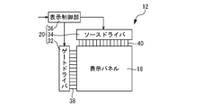
表示部12は、図2に示すように、表示パネル18と、表示パネル18を駆動制御する駆動制御部20とを備える。
表示パネル18は、液晶パネルである。簡単に説明すると、表示パネル18は、複数の画素電極(図示せず)がマトリクス状に形成されたアクティブマトリクス基板22と、対向電極(図示せず)が形成された対向基板24と、これらアクティブマトリクス基板22と対向基板24との間に封入された液晶層26とを備える。表示パネル18においては、画素電極毎に、画素28(図3参照)が形成される。複数の画素28がマトリクス状に形成された領域が、表示パネル18の表示領域になる。本実施形態では、後述する図6及び図8に示すように、観察者の右眼に映る画像(右眼用画像)を表示する画素28の列と、観察者の左眼に映る画像(左眼用画像)を表示する画素28の列とが、交互に配置される。
すなわち、本実施形態においては、右眼用画像と左眼用画像が、それぞれ、画素列毎に(ストライプ状に)分割される。そして、これらストライプ状に分割された右眼用画像及び左眼用画像を交互に並べた合成画像が表示パネル18に表示される。
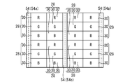
そこにおいて、本実施形態では、各画素28が複数のサブ画素30(例えば、R(赤)画素,G(緑)画素及びB(青)画素等)を備える。特に本実施形態では、図3に示すように、表示パネル18の表示領域の縦方向に沿って、複数のサブ画素30が並んでいる。アクティブマトリクス基板22には、各サブ画素30の画素電極(図示せず)が形成されている。対向基板24には、カラーフィルタ(図示せず)が形成されている。カラーフィルタに形成された、図示しない着色層(例えば、赤色層,緑色層及び青色層等)は、各サブ画素30の画素電極と対応する位置にある。
表示パネル18の駆動制御部20は、ゲートドライバ32と、ソースドライバ34と、表示制御部36とを備える。
ゲートドライバ32には、複数のゲート線38が接続されている。これら複数のゲート線38は、それぞれ、スイッチング素子としての薄膜トランジスタ(図示せず)のゲート電極(図示せず)に接続されている。薄膜トランジスタは、表示パネル18が有するアクティブマトリクス基板22上に形成されている。各ゲート線38は、ゲートドライバ32から出力される走査信号を伝送する。ゲート電極に入力される走査信号によって、薄膜トランジスタが駆動制御される。
ソースドライバ34には、複数のソース線40が接続されている。これら複数のソース線40は、それぞれ、薄膜トランジスタのソース電極(図示せず)に接続されている。各ソース線40は、ソースドライバ34から出力される表示信号を伝送する。薄膜トランジスタの駆動状態下において、薄膜トランジスタに表示信号が入力されると、表示信号に応じた電荷が、薄膜トランジスタに接続された蓄積容量(図示せず)に蓄積される。蓄積容量は、薄膜トランジスタのドレイン電極(図示せず)に接続された画素電極(図示せず)と、画素電極に対向配置された共通電極(図示せず)と、液晶層26のうち画素電極と共通電極との間に位置する部分とによって構成されている。表示信号に応じた電荷を蓄積容量に蓄積することにより、各サブ画素30の階調を制御することができる。その結果、表示パネル18において、画像を表示することができる。
表示制御部36は、外部から送られてくる表示データ信号と、タイミング制御信号とに基づいて、画像表示に必要な各種信号を生成し、ゲートドライバ32及びソースドライバ34に出力する。上述の合成画像は、表示制御部36において生成される。
表示パネル18の厚さ方向一方側には、バックライト14が配置される。バックライト14は、光源42と、反射部44とを備える。
このようなバックライト14においては、光源42から照射された光が、反射部44によって反射される。その結果、表示パネル18に、光が照射される。
なお、バックライト14としては、図1に示すようなエッジライト型の他、例えば、直下型、平面光源型等を採用することができる。また、バックライト14の光源42としては、例えば、冷陰極管や発光ダイオード(LED)等を採用することができる。
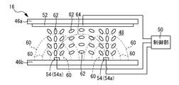
表示パネル18の厚さ方向他方側には、画像分離部16が配置される。画像分離部16は、図4に示すように、一対の基板46a,46bと、一対の基板46a,46b間に封入された液晶層48と、制御部50とを備える。
一対の基板46a,46bとしては、それぞれ、例えば、ガラス基板等を採用することができる。
一方の基板46aには、共通電極52が形成されている。共通電極52としては、例えば、透明な導電膜を採用することができる。透明な導電膜としては、例えば、インジウム酸化錫膜(ITO膜)等を採用することができる。共通電極52は、一方の基板46aにおいて他方の基板46bと対向する面の略全体に亘って形成されている。
他方の基板46bには、複数の駆動電極54が形成されている。各駆動電極54としては、例えば、透明な導電膜を採用することができる。透明な導電膜としては、例えば、インジウム酸化錫膜(ITO膜)等を採用することができる。
複数の駆動電極54は、図5に示すように、複数の第1駆動電極54aと、複数の第2駆動電極54bとを備える。なお、図5では、理解を容易にするために、第1及び第2の駆動電極54a,54bは、それぞれ、3つしか図示していないが、第1及び第2の駆動電極54a,54bの数は、任意の設計事項である。
複数の第1駆動電極54aは、それぞれ、他方の基板46bの縦方向(表示パネル18の表示領域の縦方向)に略一定の幅寸法で延びている。つまり、複数の第1駆動電極54aは、他方の基板46bの横方向(表示パネル18の表示領域の横方向)に並んでいる。
各第1駆動電極54aは、図3や、後述する図6及び図8に示すように、複数の第1駆動電極54aが並ぶ方向で隣り合う2つの画素28,28の境界上に位置している。なお、複数の第1駆動電極54aが並ぶ方向で隣り合う2つ画素28,28の境界上に各第1駆動電極54aが位置するとは、画像分離部16の平面視において、複数の第1駆動電極54aが並ぶ方向で隣り合う2つの画素28,28の境界が各第1駆動電極54aと重なることをいう。具体的には、例えば、画像分離部16の平面視において、カラーフィルタに形成されたブラックマトリクス(図示せず)と各第1駆動電極54aとが重なる場合には、複数の第1駆動電極54aが並ぶ方向で隣り合う2つ画素28,28の境界上に各第1駆動電極54aが位置することになる。
隣り合う2つの第1駆動電極54a,54aの離隔距離(第1駆動電極54aの配設ピッチ)は、複数の第1駆動電極54aが並ぶ方向での4画素分に相当する大きさとなっている(図3参照)。
各第1駆動電極54aの長さ方向一端(図5の下端)同士が、連結電極56aによって、連結されている。連結電極56aは、他方の基板46bの横方向に略一定の幅寸法で延びている。連結電極56aとしては、例えば、透明な導電膜を採用することができる。透明な導電膜としては、例えば、インジウム酸化錫膜(ITO膜)等を採用することができる。
連結電極56aの一端には、端子部58aが形成されている。端子部58aには、制御部50が接続される。
複数の第2駆動電極54bは、それぞれ、他方の基板46bの縦方向に略一定の幅寸法で延びている。つまり、複数の第2駆動電極54bは、他方の基板46bの横方向に並んでいる。
各第2駆動電極54bは、隣り合う2つの第1駆動電極54aの間に配置されている。これにより、第1駆動電極54aと第2駆動電極54bとが交互に並んでいる。
各第2駆動電極54bは、図3や、後述する図6及び図8に示すように、複数の第2駆動電極54bが並ぶ方向で隣り合う2つの画素28,28の境界上に位置している。なお、複数の第2駆動電極54bが並ぶ方向で隣り合う2つ画素28,28の境界上に各第2駆動電極54bが位置するとは、画像分離部16の平面視において、複数の第2駆動電極54bが並ぶ方向で隣り合う2つの画素28,28の境界が各第2駆動電極54bと重なることをいう。具体的には、例えば、画像分離部16の平面視において、カラーフィルタに形成されたブラックマトリクス(図示せず)と各第2駆動電極54bとが重なる場合には、複数の第2駆動電極54bが並ぶ方向で隣り合う2つの画素28,28の境界上に各第2駆動電極54bが位置することになる。
隣り合う2つの第2駆動電極54b,54bの離隔距離(第2駆動電極54bの配設ピッチ)は、複数の第2駆動電極54bが並ぶ方向での4画素分に相当する大きさとなっている。
隣り合う2つの駆動電極54,54の離隔距離(第1駆動電極54aと第2駆動電極54bの離隔距離)、即ち、駆動電極54の配設ピッチは、複数の駆動電極54が並ぶ方向での2画素分に相当する大きさとなっている。
各第2駆動電極54bの長さ方向他端(図5の上端)同士が、連結電極56bによって、連結されている。連結電極56bは、他方の基板46bの横方向に略一定の幅寸法で延びている。連結電極56bとしては、例えば、透明な導電膜を採用することができる。透明な導電膜としては、例えば、インジウム酸化錫膜(ITO膜)等を採用することができる。
連結電極56bの一端には、端子部58bが形成されている。端子部58bには、制御部50が接続される。
液晶層48の液晶としては、例えば、TN液晶、ホモジニアス液晶等を採用することができる。ホモジニアス液晶を採用する場合、一方の基板46aに形成されて、共通電極52を覆う配向膜(図示せず)の配向軸と、他方の基板46bに形成されて、複数の駆動電極54を覆う配向膜(図示せず)の配向軸とが平行になる。
制御部50は、後述する疑似的なレンズ64を液晶層48内に複数形成するために、共通電極52及び複数の駆動電極54のそれぞれに対して、適当な電圧を印加する。本実施形態では、各駆動電極54に印加する電圧として、共通電極52に印加する電圧と同じ位相の電圧と、共通電極52に印加する電圧とは逆位相の電圧とがある。なお、共通電極52及び複数の駆動電極54のそれぞれに印加する電圧としては、例えば、5Vの矩形波等がある。
制御部50は、例えば、外部からの信号に基づいて、共通電極52に印加する電圧とは逆位相の電圧を印加する駆動電極54を、複数の駆動電極54から幾つか選択する。制御部50が共通電極52に印加する電圧とは逆位相の電圧を印加する駆動電極54を選択する方法としては、例えば、(1)ユーザが操作可能な操作ボタンを立体表示装置10に設けて、ユーザによる操作内容に応じて選択する方法、(2)ユーザを撮影するカメラを立体表示装置10に設けて、当該立体表示装置10の表示画面を見ているユーザの数をカメラが撮影する画像から判断し、ユーザの数に応じて選択する方法等を採用することができる。
制御部50が、複数の駆動電極54から選択した幾つかの駆動電極54に対して、共通電極52に印加する電圧とは逆位相の電圧を印加すると、図4に示すように、等電位線60が液晶層48内に形成される。これにより、液晶層48内の液晶分子62の配向方向が変化する。その結果、疑似的なレンズ64が液晶層48内に形成される。
疑似的なレンズ64は、液晶層48内に複数形成される。これら複数の疑似的なレンズ64は、複数の駆動電極54が並ぶ方向に並んでいる。
電圧を印加する駆動電極54が変更されると、液晶層48内に形成される複数の疑似的なレンズ64は、複数の駆動電極54が並ぶ方向での位置及び大きさが変化する。これにより、立体表示装置10の視点数が変化する。
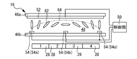
本実施形態では、液晶層48内に疑似的なレンズ64を複数形成する方法として、(1)複数の駆動電極54の全てに対して、共通電極52に印加する電圧とは逆位相の電圧を印加する方法と、(2)複数の第1駆動電極54aの全てに対して、共通電極52に印加する電圧とは逆位相の電圧を印加し、複数の第2駆動電極54bの全てに対して、共通電極52に印加する電圧と同じ位相の電圧を印加する方法とがある。
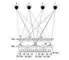
複数の駆動電極54の全てに対して、共通電極52に印加する電圧とは逆位相の電圧を印加する場合、液晶層48内に形成される疑似的なレンズ64の幅寸法(複数の駆動電極54が並ぶ方向での長さ)は、複数の駆動電極54が並ぶ方向での2画素分に相当する大きさとなっている。この場合、立体表示装置10は、図6に示すように、1視点となる。
複数の第1駆動電極54aの全てに対して、共通電極52に印加する電圧とは逆位相の電圧を印加し、複数の第2駆動電極54bの全てに対して、共通電極52に印加する電圧と同じ位相の電圧を印加する場合、図7に示すように、液晶層48内に形成される疑似的なレンズ64の幅寸法(複数の駆動電極54が並ぶ方向での長さ)は、複数の駆動電極54が並ぶ方向での4画素分に相当する大きさとなっている。この場合、立体表示装置10は、図8に示すように、4視点となる。なお、図8においては、第2駆動電極54bを破線で示している。
このような立体表示装置10においては、複数の駆動電極54が並ぶ方向で隣り合う2つの画素28,28の境界上に各駆動電極54が位置している。これにより、画像分離部16が備える液晶層48内に疑似的なレンズ64を複数形成するために必要な駆動電極54の数を少なくすることができる。
各駆動電極54に印加する電圧が2種類しかないので、複数の駆動電極54が並ぶ方向におけるレンズ64の位置及び大きさを変更する場合であっても、各駆動電極54に印加する電圧の大きさを変更する必要がなくなる。その結果、電圧の制御が容易になる。
各駆動電極54が、複数のサブ画素30が並ぶ方向に延びている。そのため、各サブ画素30の発する色が、液晶層48内に形成される疑似的なレンズ64によって、分離されるのを防ぐことができる。
複数の第1駆動電極54aの長さ方向一端同士が、連結電極56aによって、接続されている。これにより、各第1駆動電極54aに対して一斉に電圧を供給するための配線が簡単になる。
複数の第2駆動電極54bの長さ方向他端同士が、連結電極56bによって、接続されている。これにより、各第2駆動電極54bに対して一斉に電圧を供給するための配線が簡単になる。
[実施形態の応用例]
本応用例においては、図9に示すように、複数の駆動電極54のそれぞれが、これら複数の駆動電極54が並ぶ方向で隣に位置する2つの画素28,28の境界上にある。隣り合う2つの駆動電極54,54の離隔距離(駆動電極54の配設ピッチ)は、複数の駆動電極54が並ぶ方向での1画素分に相当する大きさとなっている。
本応用例においては、図9に示すように、複数の駆動電極54のそれぞれが、これら複数の駆動電極54が並ぶ方向で隣に位置する2つの画素28,28の境界上にある。隣り合う2つの駆動電極54,54の離隔距離(駆動電極54の配設ピッチ)は、複数の駆動電極54が並ぶ方向での1画素分に相当する大きさとなっている。
複数の駆動電極54は、互いに独立している。複数の駆動電極54は、例えばドライバ等の制御部により、個別に電圧が印加される。これにより、様々な視点数に切り替えることが容易になる。
以上、本発明の実施形態について、詳述してきたが、これらはあくまでも例示であって、本発明は、上述の実施形態によって、何等、限定されない。
例えば、前記実施形態において、表示パネル18は、プラズマディスプレイパネル、有機EL(Electro Luminescence)パネル、無機ELパネル等であっても良い。
前記実施形態において、共通電極52に印加する電圧を一定にし、且つ、各駆動電極54に印加する電圧を、共通電極52に印加する電圧の+側と-側とが交互に繰り返される交流電圧(矩形波)にしても良い。共通電極52に印加する電圧としては、例えば、GND等がある。
前記実施形態において、画素28は、モザイク配列であっても良いし、デルタ配列であっても良い。
図3及び図9においては、複数の駆動電極54のそれぞれが、これら複数の駆動電極54が並ぶ方向で隣り合う2つの画素28,28の境界上に位置しているが、例えば、表示パネル18の横方向の中央部分では、図3及び図9に示すように、隣り合う2つの画素28,28の境界上に駆動電極54を配置し、表示パネル18の端へ行くに従って、駆動電極54を表示パネル18の中央側へずらすようにしても良い。これにより、表示パネル18の端のほうに位置する画素28からの光を、観察者の眼に集光させることができる。表示パネル18の端へ行くに従って、駆動電極54を表示パネル18の中央側へずらすことは、任意の設計事項である。
Claims (4)
- 互いに異なる複数の画像をそれぞれ分割し、これらの分割画像を所定の順番に並べることで形成された合成画像を表示する表示部と、
前記合成画像に含まれる前記複数の画像を分離する画像分離部とを備え、
前記表示部は、
前記合成画像の表示に用いる画素が複数形成された表示パネルを備え、
前記画像分離部は、
一対の基板と、
前記一対の基板間に封入された液晶層と、
前記一対の基板の一方に形成された共通電極と、
前記一対の基板の他方に形成されて、互いに同じ方向に延びる複数の駆動電極と、
前記複数の駆動電極から選択した幾つかの駆動電極に、前記共通電極に印加する電圧とは異なる電圧を印加して、前記液晶層内の屈折率分布を変化させることで、前記液晶層内に疑似的なレンズを複数形成する制御部とを備え、
前記複数の駆動電極は、それぞれ、前記複数の駆動電極が並ぶ方向で隣り合う2つの前記画素の境界上に位置し、
前記制御部は、前記共通電極に印加する電圧とは異なる電圧を印加する前記駆動電極を変更することで、前記複数の駆動電極が並ぶ方向での前記レンズの位置及び形状を変化させる、立体表示装置。 - 前記画素が、互いに異なる色を発する複数のサブ画素を備え、
前記複数の駆動電極は、それぞれ、前記複数のサブ画素が並ぶ方向に延びる、請求項1に記載の立体表示装置。 - 前記複数の駆動電極が、
互いに同じ方向に延び、一方の端部同士が相互に連結された複数の第1駆動電極と、
互いに同じ方向に延び、第1駆動電極と交互に配置され、前記第1駆動電極における連結側端部とは反対側に位置する端部同士が相互に連結された複数の第2駆動電極とを備える、請求項1又は2に記載の立体表示装置。 - 前記表示パネルが液晶パネルである、請求項1~3の何れか1項に記載の立体表示装置。
Applications Claiming Priority (2)
| Application Number | Priority Date | Filing Date | Title |
|---|---|---|---|
| JP2011-088357 | 2011-04-12 | ||
| JP2011088357 | 2011-04-12 |
Publications (1)
| Publication Number | Publication Date |
|---|---|
| WO2012141078A1 true WO2012141078A1 (ja) | 2012-10-18 |
Family
ID=47009253
Family Applications (1)
| Application Number | Title | Priority Date | Filing Date |
|---|---|---|---|
| PCT/JP2012/059385 Ceased WO2012141078A1 (ja) | 2011-04-12 | 2012-04-05 | 立体表示装置 |
Country Status (1)
| Country | Link |
|---|---|
| WO (1) | WO2012141078A1 (ja) |
Cited By (2)
| Publication number | Priority date | Publication date | Assignee | Title |
|---|---|---|---|---|
| CN103901625A (zh) * | 2012-12-25 | 2014-07-02 | 联想(北京)有限公司 | 显示控制方法和显示设备 |
| EP3244259A4 (en) * | 2015-01-06 | 2018-01-24 | Huawei Technologies Co. Ltd. | Display apparatus, stereoscopic display apparatus, and terminal applying the same |
Citations (3)
| Publication number | Priority date | Publication date | Assignee | Title |
|---|---|---|---|---|
| JP2000102038A (ja) * | 1998-09-18 | 2000-04-07 | Sanyo Electric Co Ltd | 2次元映像/3次元映像互換型映像表示装置 |
| JP2010224191A (ja) * | 2009-03-23 | 2010-10-07 | Toshiba Corp | 立体画像表示装置 |
| JP2011154197A (ja) * | 2010-01-27 | 2011-08-11 | Sony Corp | 立体表示装置 |
-
2012
- 2012-04-05 WO PCT/JP2012/059385 patent/WO2012141078A1/ja not_active Ceased
Patent Citations (3)
| Publication number | Priority date | Publication date | Assignee | Title |
|---|---|---|---|---|
| JP2000102038A (ja) * | 1998-09-18 | 2000-04-07 | Sanyo Electric Co Ltd | 2次元映像/3次元映像互換型映像表示装置 |
| JP2010224191A (ja) * | 2009-03-23 | 2010-10-07 | Toshiba Corp | 立体画像表示装置 |
| JP2011154197A (ja) * | 2010-01-27 | 2011-08-11 | Sony Corp | 立体表示装置 |
Cited By (3)
| Publication number | Priority date | Publication date | Assignee | Title |
|---|---|---|---|---|
| CN103901625A (zh) * | 2012-12-25 | 2014-07-02 | 联想(北京)有限公司 | 显示控制方法和显示设备 |
| EP3244259A4 (en) * | 2015-01-06 | 2018-01-24 | Huawei Technologies Co. Ltd. | Display apparatus, stereoscopic display apparatus, and terminal applying the same |
| US10302958B2 (en) | 2015-01-06 | 2019-05-28 | Huawei Technologies Co., Ltd. | Display apparatus, stereoscopic display apparatus, and application terminal thereof |
Similar Documents
| Publication | Publication Date | Title |
|---|---|---|
| US9091884B2 (en) | Display apparatus | |
| US9213203B2 (en) | Three-dimensional image display | |
| RU2721752C2 (ru) | Устройство отображения и способ управления отображением | |
| KR101756671B1 (ko) | 입체 영상 표시 장치 및 그 구동 방법 | |
| US8587737B2 (en) | Display device | |
| JP2012234142A (ja) | 表示装置 | |
| JP2011043623A (ja) | 立体映像表示装置 | |
| CN102749715B (zh) | 可切换二维与三维显示模式的显示装置 | |
| US20130077037A1 (en) | Liquid crystal grating module and two dimension-three dimension switchable liquid crystal display device using the same | |
| CN106896519B (zh) | 一种三维显示装置及其驱动方法 | |
| WO2012137879A1 (ja) | 表示装置 | |
| US10061136B2 (en) | Display device and method for controlling the same | |
| KR102144733B1 (ko) | 입체 영상 디스플레이 장치 | |
| WO2015060011A1 (ja) | 立体表示装置 | |
| JP4200056B2 (ja) | 表示装置 | |
| WO2013080927A1 (ja) | 立体表示装置 | |
| JP2012037808A (ja) | 立体表示装置および液晶バリア装置 | |
| WO2012169466A1 (ja) | 表示装置 | |
| US8749742B2 (en) | Display device and liquid crystal element | |
| CN108370439B (zh) | 显示设备和显示控制方法 | |
| JP2013057824A (ja) | 表示装置、表示方法、および電子機器 | |
| WO2012070469A1 (ja) | 立体表示装置 | |
| KR20120070913A (ko) | 2d/3d영상 표시 장치 | |
| US9007363B2 (en) | Display apparatus and method of displaying three dimensional image | |
| KR20160004475A (ko) | 입체영상 표시장치 |
Legal Events
| Date | Code | Title | Description |
|---|---|---|---|
| 121 | Ep: the epo has been informed by wipo that ep was designated in this application |
Ref document number: 12770959 Country of ref document: EP Kind code of ref document: A1 |
|
| NENP | Non-entry into the national phase |
Ref country code: DE |
|
| 122 | Ep: pct application non-entry in european phase |
Ref document number: 12770959 Country of ref document: EP Kind code of ref document: A1 |
|
| NENP | Non-entry into the national phase |
Ref country code: JP |