WO2012132224A1 - Pressure-sensitive switch - Google Patents
Pressure-sensitive switch Download PDFInfo
- Publication number
- WO2012132224A1 WO2012132224A1 PCT/JP2012/001337 JP2012001337W WO2012132224A1 WO 2012132224 A1 WO2012132224 A1 WO 2012132224A1 JP 2012001337 W JP2012001337 W JP 2012001337W WO 2012132224 A1 WO2012132224 A1 WO 2012132224A1
- Authority
- WO
- WIPO (PCT)
- Prior art keywords
- electrodes
- pressure
- sensitive switch
- electrode
- pressing member
- Prior art date
Links
Images


Classifications
-
- H—ELECTRICITY
- H03—ELECTRONIC CIRCUITRY
- H03K—PULSE TECHNIQUE
- H03K17/00—Electronic switching or gating, i.e. not by contact-making and –breaking
- H03K17/94—Electronic switching or gating, i.e. not by contact-making and –breaking characterised by the way in which the control signals are generated
- H03K17/96—Touch switches
- H03K17/9625—Touch switches using a force resistance transducer
-
- H—ELECTRICITY
- H01—ELECTRIC ELEMENTS
- H01H—ELECTRIC SWITCHES; RELAYS; SELECTORS; EMERGENCY PROTECTIVE DEVICES
- H01H13/00—Switches having rectilinearly-movable operating part or parts adapted for pushing or pulling in one direction only, e.g. push-button switch
- H01H13/70—Switches having rectilinearly-movable operating part or parts adapted for pushing or pulling in one direction only, e.g. push-button switch having a plurality of operating members associated with different sets of contacts, e.g. keyboard
- H01H13/78—Switches having rectilinearly-movable operating part or parts adapted for pushing or pulling in one direction only, e.g. push-button switch having a plurality of operating members associated with different sets of contacts, e.g. keyboard characterised by the contacts or the contact sites
- H01H13/785—Switches having rectilinearly-movable operating part or parts adapted for pushing or pulling in one direction only, e.g. push-button switch having a plurality of operating members associated with different sets of contacts, e.g. keyboard characterised by the contacts or the contact sites characterised by the material of the contacts, e.g. conductive polymers
-
- H—ELECTRICITY
- H01—ELECTRIC ELEMENTS
- H01H—ELECTRIC SWITCHES; RELAYS; SELECTORS; EMERGENCY PROTECTIVE DEVICES
- H01H2201/00—Contacts
- H01H2201/022—Material
- H01H2201/032—Conductive polymer; Rubber
- H01H2201/036—Variable resistance
-
- H—ELECTRICITY
- H01—ELECTRIC ELEMENTS
- H01H—ELECTRIC SWITCHES; RELAYS; SELECTORS; EMERGENCY PROTECTIVE DEVICES
- H01H2203/00—Form of contacts
- H01H2203/02—Interspersed fingers
Definitions
- the present invention relates to a pressure sensitive switch mainly used for operation of various electronic devices.
- FIG. 7 is an exploded perspective view of a conventional pressure sensitive switch.
- FIG. 8 is a cross-sectional view of a conventional pressure sensitive switch.
- the pressure-sensitive switch 20 includes a pressure-sensitive conductive sheet 5, an electrode pair 15, and a pressing member 16.
- the pressure-sensitive conductive sheet 5 includes a substrate 1, a low resistance layer 2, a high resistance layer 3, and a spacer 4.
- the material of the flexible substrate 1 is polyethylene terephthalate or the like.
- the low resistance layer 2 and the high resistance layer 3 are formed on the lower surface of the substrate 1 by screen printing or the like.
- the annular spacer 4 is attached to the lower surface of the high resistance layer 3.
- the low resistance layer 2 has a sheet resistance value of 50 ⁇ / ⁇ to 30 k ⁇ / ⁇ and is formed of phenol or the like in which carbon powder is dispersed.
- the high resistance layer 3 has a sheet resistance value of 50 k ⁇ / ⁇ to 5 M ⁇ / ⁇ and is formed of phenol or the like in which carbon powder is dispersed. A large number of spherical particles 6 are mixed in the high resistance layer 3, and the particles 6 form irregularities on the lower surface of the high resistance layer 3.
- the comb-like electrode pair 15 is disposed on the substrate 11 and includes electrodes 12A to 12D and electrodes 13A to 13C.
- the pressure-sensitive conductive sheet 5 is disposed above the electrode pair 15, and the electrode pair 15 and the high resistance layer 3 face each other.
- the pressing member 16 moves up and down by the operation of the operator.
- the pressing member 16 is disposed on the upper surface of the pressure-sensitive conductive sheet 5.
- the pressure-sensitive switch 20 is disposed on the front surface of a casing of various electronic devices such as a mobile phone and a car navigation system, and moves and displays a cursor (not shown) displayed on a liquid crystal display (not shown) of the electronic device. Used for.
- the electrodes 12A to 12D and the electrodes 13A to 13C and the lower surface of the high resistance layer 3 come into contact with each other.
- the contact area between the high resistance layer 3 and the electrodes 12A to 12D and the electrodes 13A to 13C increases as the pressing force of the operator increases.
- the electrodes 12A to 12D and the electrodes 13A to 13C are electrically connected via the high resistance layer 3.
- the resistance value between the electrodes 12A to 12D and the electrodes 13A to 13C changes. Due to the change in the resistance value, the output voltage of the electrode pair 15 to the control circuit (not shown) of the electronic device changes.
- the control circuit changes, for example, the speed at which the cursor displayed on the liquid crystal display is moved and displayed in accordance with the change in voltage.
- Patent Document 1 is known as prior art document information related to the invention of this application.
- the present invention is a pressure-sensitive switch that can be easily operated by an operator when the input voltage to the control circuit changes gently with respect to the pressing force.
- the pressure-sensitive switch includes a pressing member pressed by an operator, a base material disposed below the pressing member, a resistor printed on the bottom surface of the base material, and an electric circuit facing the base material in parallel.
- the electrode that comes into contact with the resistor first by the pressing of the pressing member is electrically connected in parallel with the other electrode via the resistance element.
- the change in the resistance value of the electrode pair can be made gentle with respect to the change in the pressing force of the pressing member, and the input voltage to the control circuit changes gradually with respect to the pressing force.
- FIG. 1 is an exploded perspective view showing a pressure-sensitive switch according to an embodiment of the present invention.
- FIG. 2 is a cross-sectional view of the pressure-sensitive switch according to the embodiment of the present invention.
- FIG. 3A is a cross-sectional view showing a pressed state of the pressure-sensitive switch in the embodiment of the present invention.
- FIG. 3B is a cross-sectional view showing a pressed state of the pressure-sensitive switch according to the embodiment of the present invention.
- FIG. 4A is a circuit diagram of an electrode pair used in the pressure-sensitive switch according to the embodiment of the present invention.
- FIG. 4B is a circuit diagram for explaining the operation of the electrode pair used in the pressure-sensitive switch according to the embodiment of the present invention.
- FIG. 5A is a graph showing a change in resistance value with respect to the pressing force of the pressure-sensitive switch according to the embodiment of the present invention.
- FIG. 5B is a graph showing a change in voltage with respect to the pressing force of the pressure-sensitive switch according to the embodiment of the present invention.
- FIG. 6A is a top view of a substrate for explaining an electrode pattern used in the pressure-sensitive switch according to the embodiment of the present invention.
- FIG. 6B is a top view of the substrate for explaining another pattern of electrodes used in the pressure-sensitive switch according to the embodiment of the present invention.
- FIG. 6C is a top view of the substrate for explaining another pattern of the electrodes used in the pressure-sensitive switch according to the embodiment of the present invention.
- FIG. 7 is an exploded perspective view of a conventional pressure sensitive switch.
- FIG. 8 is a cross-sectional view of a conventional pressure sensitive switch.
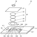
- FIG. 1 is an exploded perspective view showing a pressure-sensitive switch 40 according to an embodiment of the present invention.
- the pressure sensitive switch 40 includes a pressing member 36, a base member 21, a high resistance layer 24, a plurality of electrodes 32A to 32D and electrodes 33A to 33C, and a resistance connected to at least one electrode.
- An element 34 is provided.
- the base material 21 is disposed below the pressing member 36, and the high resistance layer 24 is a resistor and is printed on the lower surface of the base material 21.
- the electrode 33B that first contacts the resistor by the pressing of the pressing member is electrically connected in parallel with the other electrodes 33A and 33C via the resistance element 34.
- the resistance value of the electrode pair 35 including the electrodes 32A to 32D and the electrodes 33A to 33C can be moderately changed with respect to the pressing force of the pressing member 36.
- the pressure-sensitive switch 40 that allows easy operation of the electronic device such as adjusting the moving speed of a cursor (not shown) displayed on the electronic device (not shown) to a desired speed.
- the low resistance layer 2 and the high resistance layer 3 are very thin, and even if the pressing force on the upper surface of the pressing member 16 is small, The resistance value between the electrodes 12A to 12D and the electrodes 13A to 13C immediately decreases. Therefore, even if the operator tries to adjust the moving speed of the cursor or the like to a desired speed, it is difficult to press the pressing member 16 with an appropriate pressing force, which hinders easy operation.
- the pressure sensitive switch having the configuration of the present embodiment changes the resistance value of the electrode pair 35 including the electrodes 32A to 32D and the electrodes 33A to 33C with respect to the change of the pressing force of the pressing member 36. It can be gradual.
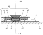
- FIG. 2 is a cross-sectional view of the pressure-sensitive switch 40 according to the embodiment of the present invention.
- the pressure-sensitive switch 40 includes a pressure-sensitive conductive sheet 26, an electrode pair 35, and a pressing member 36.
- the pressure-sensitive conductive sheet 26 includes a base material 21, a low resistance layer 22, a medium resistance layer 23, a high resistance layer 24, and a spacer 25.
- the flexible base material 21 is made of polyethylene terephthalate or the like.
- a low resistance layer 22, a medium resistance layer 23, and a high resistance layer 24 are formed on the lower surface of the substrate 21, and an annular spacer 25 is attached to the lower surface of the high resistance layer 24.
- the sheet resistance value of the middle resistor layer 23 is between the sheet resistance value of the high resistor layer 24 and the sheet resistance value of the low resistor layer 22, and the sheet resistance value of the low resistor layer 22 is the lowest.
- the sheet resistance value of the low resistance layer 22 is 50 ⁇ / ⁇ to 20 k ⁇ / ⁇
- the sheet resistance value of the medium resistance layer 23 is 20 k ⁇ / ⁇ to 80 k ⁇ / ⁇
- the sheet resistance value of the high resistance layer 24 is 80 k ⁇ / ⁇ .
- ⁇ ⁇ 5M ⁇ / ⁇ is more suitable.
- the thicknesses of the low resistance layer 22, the middle resistance layer 23, and the high resistance layer 24 are all about 1 to 50 ⁇ m and are formed by screen printing or the like.
- a large number of spherical particles 27 are mixed in the high resistance layer 24, which is an example of a resistor, and irregularities are formed on the lower surface of the high resistance layer 24 by the particles 27.
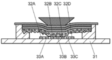
- the comb-like electrode pair 35 is configured on the upper surface of the substrate 31.
- the electrode pair 35 includes electrodes 32A to 32D, electrodes 33A to 33C, and a resistance element 34.
- the electrode pair 35 is electrically connected to the power source at the left terminal A11, and is connected to the ground potential via a pull-down resistor at the right terminal B11.
- the electrodes 32A to 32D are connected to the terminal A11.
- the electrodes 33A and 33C are connected to the terminal B11, and the electrode 33B is connected to the terminal B11 via the resistance element 34.
- the pressure-sensitive conductive sheet 26 is disposed above the electrode pair 35, and the electrode pair 35 and the high resistance layer 24 face each other.
- a pressing member 36 that moves up and down by an operator's operation is disposed on the upper surface of the pressure-sensitive conductive sheet 26.
- the pressure-sensitive switch 40 configured in this manner is arranged on the front surface of the casing of various electronic devices such as a mobile phone and a car navigation system. For example, a cursor (not shown) displayed on a liquid crystal display (not shown) of the electronic device. Used to move and display.
- the contact area between the high resistance layer 24 and the electrodes 32A to 32D and the electrodes 33A to 33C increases as the pressing force of the operator increases.
- the electrodes 32A to 32D and the electrodes 33A to 33C are electrically connected through the high resistance layer 24.
- a resistance value change between the electrodes 32A to 32D or the electrodes 33A to 33C causes an electrode pair to be connected to a control circuit (not shown) of the electronic device.
- the voltage input from 35 changes.
- the control circuit changes the speed of moving and displaying the cursor displayed on the liquid crystal display or the like in accordance with the change in voltage.
- FIG. 3A is a cross-sectional view of the pressure-sensitive switch 40 taken along the electrode 33B.
- 3B is a cross-sectional view of the 3B-3B cross section in FIG. 3A.
- the electrode 33B and the high resistance layer 24 first come into contact with each other.
- the high resistance layer 24 is also in contact with, for example, the electrodes 32B and 32C, and the electrode 33B is electrically connected to the electrodes 32B and 32C through the high resistance layer 24.
- the electrodes 32A, 32D, 33A, and 33C are sequentially increased from the electrode closer to the electrode 33B that first contacts the high resistance layer 24. Contact with the resistor layer 24.
- FIG. 4A is a circuit diagram of the electrode pair 35.
- 4B is a circuit diagram in which the connection between the electrode 33A and the resistance element 34 and the connection between the electrode 33C and the resistance element 34 are disconnected. Note that FIG. 4B is shown as a hypothesis, and is a diagram for explaining a change in resistance value regarding each of the electrodes 33A to 33C.
- terminal A11 is connected to a power source among both ends of electrode pair 35, and terminal B11 serving as an output terminal of electrode pair 35 is connected to the ground potential via a pull-down resistance element.
- terminals B12 to B14 are output terminals related to the electrode 33A, the electrode 33B, the resistance element 34, and the electrode 33C, respectively.
- the resistance value between the terminal A11 and the terminal B11 in FIG. 4A is the resistance value between the terminal A11 and the terminal B12 in FIG. 4B, the resistance value between the terminal A11 and the terminal B13, and the resistance value between the terminal A11 and the terminal B14.
- the combined resistance value is the resistance value between the terminal A11 and the terminal B12 in FIG. 4B.
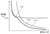
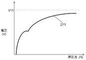
- FIG. 5A shows a graph showing changes in these resistance values with respect to the pressing force of the operator.
- FIG. 5B is a graph showing a change in the output voltage of the terminal B11 with respect to the pressing force of the operator.
- the curve C11 is the resistance value between the terminal A11 and the terminal B11
- the curve C12 is the resistance value between the terminal A11 and the terminal B13
- the curve C13 is the resistance value between the terminal A11 and the terminal B12
- the resistance value is shown. Note that the resistance value between the terminal A11 and the terminal B12 and the resistance value between the terminal A11 and the terminal B14 are substantially the same, and are represented by a curve C13.
- the curve D11 indicates the output voltage of the terminal B11.
- the curve D11 changes in inverse proportion to the change of the curve C11 in FIG. 5A.
- the curve C12 has a large contact area between the electrode 33B and the high resistance layer 24 even if the pressing force is small because the electrode 33B first contacts the lower surface of the high resistance layer 24. Therefore, it changes even with a small pressing force and converges to a resistance value R11 which is a predetermined resistance value of the resistance element 34.
- the resistance value R11 is preferably 10 k ⁇ or more and 10 M ⁇ or less.
- the contact resistance values of the electrodes 33A and 33C gradually decrease after the pressing force increases as shown by the curve C13.
- the resistance value between the terminal A11 and the terminal B11 indicated by the curve C11 is greatly influenced by the curve C12 in the region where the pressing force is small, whereas the influence of the curve C13 is large in the region where the pressing force is large. It changes gradually with respect to changes in
- the curve D11 changes gently with respect to the change in the pressing force as a whole, just like the curve C11 changes gently with respect to the change in the pressing force as a whole.
- the resistance element 34 is connected to the electrode 33B that first contacts the high resistance layer 24 as compared with the conventional pressure sensitive switch 20, and therefore, the pressure sensitive switch 40 is between the high resistance layer 24 and the electrode 33B.
- the influence of the change in the contact resistance value on the change in the resistance of the electrode pair 35 can be mitigated.
- the resistance value of the electrode pair 35 changes gently when the pressing force of the pressing member 36 changes.
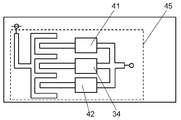
- FIG. 6A is a top view of the substrate 31 showing an example of the wiring pattern of the electrode pair 35.
- FIG. 6B is a top view of the substrate 31 showing an example of the wiring pattern of the electrode pair 45.
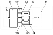
- FIG. 6C is a top view of the substrate 31 showing an example of the wiring pattern of the electrode pair 55.
- the line widths of the electrodes 32A to 32D and 33A to 33C are 0.1 mm, and the electrodes are arranged at intervals of 0.1 mm, such as between the electrodes 32A and 33A. .
- the electrodes 32A to 32D are arranged in parallel at the portions in contact with the high resistance layer 24, respectively.
- the electrodes 33A to 33C are also arranged in parallel at the portion in contact with the high resistance layer 24.
- the electrode 33B that first contacts the high resistance layer 24 is electrically connected in parallel to the electrodes 33A and 33C via the resistance element.
- the electrodes 33A to 33C are arranged in parallel at a portion in contact with the high-resistance body layer 24 serving as a resistor.
- the electrodes 33A to 33C are sequentially arranged from the electrode closest to the electrode in contact with the high-resistance body layer 24 by pressing of the pressing member 36 in order. Contact the body layer 24.
- FIG. 6B is different from FIG. 6A in that a resistance element 41 is connected to the electrode 33A and a resistance element 42 is connected to the electrode 33C. Even if the resistance elements 41 and 42 are connected to the electrodes 33A and 33C, the resistance values of the resistance elements 41 and 42 only need to be smaller than that of the resistance element 34.
- the electrode 51 in FIG. 6C is not a comb-teeth shape but a square shape, and the electrodes 52A to 52D have a change in width. As shown in FIG. 6C, the shape of the electrode may not be the shape of a comb-like electrode. The plurality of electrodes 52A to 52D may be electrically connected in parallel.
- Resistance elements 53 and 54 are electrically connected to the electrode 52B and the electrode 52C, respectively. Of the electrodes 52B and 52C, the resistance value of the resistance element connected to the electrode that first contacts the high resistance layer 24 is increased.
- the low resistor layer 22 or the medium resistor layer 23 is not necessarily required, and the high resistor layer 24 may be provided.
- the high resistance layer 24 does not necessarily require the mixing of the particles 27, and it is sufficient if the lower surface is provided with irregularities.
- the pressure-sensitive switch according to the present invention has an advantageous effect that it can be easily operated by an operator, and is mainly useful for operating various electronic devices.
Abstract
A pressure-sensitive switch has a pressing member, a base material disposed below the pressing member, a resistive element printed on the lower surface of the base material, and a plurality of electrodes facing the base material and electrically connected in parallel with each other. An electrode that first contacts the resistive element by pressing of the pressing member is electrically connected in parallel with the other electrodes through a resistor element. This makes it possible to mitigate the change in the resistance value of an electrode pair with respect to the change in the pressing force of the pressing member, so that an input voltage to a control circuit changes slowly with respect to the pressing force.
Description
本発明は、主に各種電子機器の操作に用いられる感圧スイッチに関する。
The present invention relates to a pressure sensitive switch mainly used for operation of various electronic devices.
近年、携帯電話やカーナビ等の各種電子機器の高機能化や多様化が進むに伴い、多様で確実な操作の可能な感圧スイッチが求められている。
In recent years, as electronic devices such as mobile phones and car navigation systems become more sophisticated and diversified, pressure sensitive switches that can be operated in a variety of ways are required.
従来の感圧スイッチについて、図7及び図8を用いて説明する。図7は従来の感圧スイッチの分解斜視図である。図8は従来の感圧スイッチの断面図である。
A conventional pressure-sensitive switch will be described with reference to FIGS. FIG. 7 is an exploded perspective view of a conventional pressure sensitive switch. FIG. 8 is a cross-sectional view of a conventional pressure sensitive switch.
感圧スイッチ20は、感圧導電シート5と電極対15と押圧部材16を備える。
The pressure-sensitive switch 20 includes a pressure-sensitive conductive sheet 5, an electrode pair 15, and a pressing member 16.
感圧導電シート5は、基材1と、低抵抗体層2と、高抵抗体層3と、スペーサ4を備える。
The pressure-sensitive conductive sheet 5 includes a substrate 1, a low resistance layer 2, a high resistance layer 3, and a spacer 4.
可撓性の基材1の材料は、ポリエチレンテレフタレートなどである。低抵抗体層2、高抵抗体層3は、基材1の下面にスクリーン印刷などで形成される。環状のスペーサ4は、高抵抗体層3の下面に貼り付けられる。
The material of the flexible substrate 1 is polyethylene terephthalate or the like. The low resistance layer 2 and the high resistance layer 3 are formed on the lower surface of the substrate 1 by screen printing or the like. The annular spacer 4 is attached to the lower surface of the high resistance layer 3.
低抵抗体層2は、シート抵抗値50Ω/□~30kΩ/□で、カーボン粉を分散したフェノールなどで形成される。
The low resistance layer 2 has a sheet resistance value of 50Ω / □ to 30 kΩ / □ and is formed of phenol or the like in which carbon powder is dispersed.
高抵抗体層3はシート抵抗値50kΩ/□~5MΩ/□で、カーボン粉を分散したフェノールなどで形成される。高抵抗体層3には多数の球状の粒子6が混合され、粒子6により高抵抗体層3の下面に凹凸が形成される。
The high resistance layer 3 has a sheet resistance value of 50 kΩ / □ to 5 MΩ / □ and is formed of phenol or the like in which carbon powder is dispersed. A large number of spherical particles 6 are mixed in the high resistance layer 3, and the particles 6 form irregularities on the lower surface of the high resistance layer 3.
櫛歯状の電極対15は基板11上に配置され、電極12A~12D、電極13A~13Cを備える。感圧導電シート5が電極対15の上方に配置され、電極対15と高抵抗体層3が対向する。
The comb-like electrode pair 15 is disposed on the substrate 11 and includes electrodes 12A to 12D and electrodes 13A to 13C. The pressure-sensitive conductive sheet 5 is disposed above the electrode pair 15, and the electrode pair 15 and the high resistance layer 3 face each other.
押圧部材16は、操作者の操作により上下動する。押圧部材16は感圧導電シート5の上面に配置される。
The pressing member 16 moves up and down by the operation of the operator. The pressing member 16 is disposed on the upper surface of the pressure-sensitive conductive sheet 5.
感圧スイッチ20は、携帯電話やカーナビ等の各種電子機器の筐体前面などに配置され、電子機器の液晶ディスプレイ(図示せず)などに表示されたカーソル(図示せず)などを移動表示するために用いられる。
The pressure-sensitive switch 20 is disposed on the front surface of a casing of various electronic devices such as a mobile phone and a car navigation system, and moves and displays a cursor (not shown) displayed on a liquid crystal display (not shown) of the electronic device. Used for.
操作者が感圧スイッチ20の押圧部材16の上面を押圧すると、電極12A~12D及び電極13A~13Cと高抵抗体層3の下面が接触する。
When the operator presses the upper surface of the pressing member 16 of the pressure sensitive switch 20, the electrodes 12A to 12D and the electrodes 13A to 13C and the lower surface of the high resistance layer 3 come into contact with each other.
高抵抗体層3の下面には凹凸が形成されているため、操作者の押圧力が大きいほど、高抵抗体層3と電極12A~12D及び電極13A~13Cの接触面積が増加する。
Since unevenness is formed on the lower surface of the high resistance layer 3, the contact area between the high resistance layer 3 and the electrodes 12A to 12D and the electrodes 13A to 13C increases as the pressing force of the operator increases.
電極12A~12Dと電極13A~13Cは高抵抗体層3を介して電気的に接続している。電極12A~12Dと高抵抗体層3との間、及び電極13A~13Cと高抵抗体層3との間の接触面積が大きいほど、電極12A~12Dと電極13A~13Cとの間の抵抗値は小さくなる。
The electrodes 12A to 12D and the electrodes 13A to 13C are electrically connected via the high resistance layer 3. The larger the contact area between the electrodes 12A to 12D and the high resistance layer 3 and between the electrodes 13A to 13C and the high resistance layer 3, the greater the resistance value between the electrodes 12A to 12D and the electrodes 13A to 13C. Becomes smaller.
操作者が感圧スイッチ20の押圧部材16の上面を押圧すると、電極12A~12Dと電極13A~13Cとの間の抵抗値が変化する。この抵抗値の変化により、電子機器の制御回路(図示せず)に対する電極対15の出力電圧が変化する。制御回路はこの電圧の変化に従って、例えば、液晶ディスプレイなどに表示されたカーソルを移動表示する速度を変化させる。
When the operator presses the upper surface of the pressing member 16 of the pressure sensitive switch 20, the resistance value between the electrodes 12A to 12D and the electrodes 13A to 13C changes. Due to the change in the resistance value, the output voltage of the electrode pair 15 to the control circuit (not shown) of the electronic device changes. The control circuit changes, for example, the speed at which the cursor displayed on the liquid crystal display is moved and displayed in accordance with the change in voltage.
なお、この出願の発明に関連する先行技術文献情報としては、例えば、特許文献1が知られている。
For example, Patent Document 1 is known as prior art document information related to the invention of this application.
しかしながら、従来の感圧スイッチ20においては、適切な押圧力で押圧部材16を押圧することが難しく、容易な操作の妨げとなっていた。
However, in the conventional pressure-sensitive switch 20, it is difficult to press the pressing member 16 with an appropriate pressing force, which hinders easy operation.
本発明は、押圧力に対して緩やかに制御回路への入力電圧が変化することにより、操作者が容易に操作できる感圧スイッチである。
The present invention is a pressure-sensitive switch that can be easily operated by an operator when the input voltage to the control circuit changes gently with respect to the pressing force.
本発明の感圧スイッチは、操作者が押圧する押圧部材と、押圧部材の下方に配置された基材と、基材の下面に印刷された抵抗体と、基材に対向し並列に電気的に接続された複数の電極と、少なくとも一つの電極に接続された抵抗素子とを備えている。ここで、押圧部材の押圧により最初に抵抗体に接する電極は、抵抗素子を介して他の電極と並列に電気的に接続される。
The pressure-sensitive switch according to the present invention includes a pressing member pressed by an operator, a base material disposed below the pressing member, a resistor printed on the bottom surface of the base material, and an electric circuit facing the base material in parallel. A plurality of electrodes connected to each other and a resistance element connected to at least one electrode. Here, the electrode that comes into contact with the resistor first by the pressing of the pressing member is electrically connected in parallel with the other electrode via the resistance element.
これにより、電極対の抵抗値の変化を押圧部材の押圧力の変化に対し緩やかなものとすることができ、押圧力に対して緩やかに制御回路への入力電圧が変化する。
Thereby, the change in the resistance value of the electrode pair can be made gentle with respect to the change in the pressing force of the pressing member, and the input voltage to the control circuit changes gradually with respect to the pressing force.
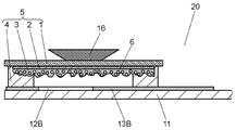
以下、本発明の実施の形態における感圧スイッチについて図面を参照しながら説明する。図面は構成を判り易くするために、部分的に寸法を拡大して示している。図1は、本発明の実施の形態における感圧スイッチ40を示す分解斜視図である。
Hereinafter, a pressure-sensitive switch according to an embodiment of the present invention will be described with reference to the drawings. In the drawings, the dimensions are partially enlarged for easy understanding of the configuration. FIG. 1 is an exploded perspective view showing a pressure-sensitive switch 40 according to an embodiment of the present invention.
本実施の形態における感圧スイッチ40は、押圧部材36と、基材21と、高抵抗体層24と、複数の電極32A~32D及び電極33A~33Cと、少なくとも一つの電極に接続された抵抗素子34を備える。
The pressure sensitive switch 40 according to the present embodiment includes a pressing member 36, a base member 21, a high resistance layer 24, a plurality of electrodes 32A to 32D and electrodes 33A to 33C, and a resistance connected to at least one electrode. An element 34 is provided.
ここで、基材21は押圧部材36の下方に配置され、高抵抗体層24は抵抗体で、基材21の下面に印刷される。また、並列に電気的に接続された複数の電極32A~32D及び電極33A~33Cは基材21に対向しており、そのうち、少なくとも一つの電極には、抵抗素子34が接続される。
Here, the base material 21 is disposed below the pressing member 36, and the high resistance layer 24 is a resistor and is printed on the lower surface of the base material 21. The plurality of electrodes 32A to 32D and the electrodes 33A to 33C electrically connected in parallel face the base member 21, and a resistance element 34 is connected to at least one of the electrodes.
また、押圧部材の押圧により最初に抵抗体に接する電極33Bは、抵抗素子34を介して他の電極33A及び33Cと並列に電気的に接続される。
Also, the electrode 33B that first contacts the resistor by the pressing of the pressing member is electrically connected in parallel with the other electrodes 33A and 33C via the resistance element 34.
このような構成により、電極32A~32D及び電極33A~33Cを備える電極対35の抵抗値の変化を押圧部材36の押圧力の変化に対し緩やかなものとすることができる。
With such a configuration, the resistance value of the electrode pair 35 including the electrodes 32A to 32D and the electrodes 33A to 33C can be moderately changed with respect to the pressing force of the pressing member 36.
したがって、電子機器(図示せず)に表示されたカーソル(図示せず)の移動速度を所望の速度に調整するなど電子機器の操作が容易な感圧スイッチ40が提供される。
Therefore, it is possible to provide the pressure-sensitive switch 40 that allows easy operation of the electronic device such as adjusting the moving speed of a cursor (not shown) displayed on the electronic device (not shown) to a desired speed.
即ち、図7、8に示すように、従来の感圧スイッチ20においては、低抵抗体層2や高抵抗体層3は非常に薄く、押圧部材16の上面への押圧力が小さくても、電極12A~12Dと電極13A~13Cとの間の抵抗値がすぐに小さくなる。そのため、カーソルなどが移動する速度を操作者が所望の速度に調整しようとしても、適切な押圧力で押圧部材16を押圧することが難しく、容易な操作の妨げとなっていた。
That is, as shown in FIGS. 7 and 8, in the conventional pressure sensitive switch 20, the low resistance layer 2 and the high resistance layer 3 are very thin, and even if the pressing force on the upper surface of the pressing member 16 is small, The resistance value between the electrodes 12A to 12D and the electrodes 13A to 13C immediately decreases. Therefore, even if the operator tries to adjust the moving speed of the cursor or the like to a desired speed, it is difficult to press the pressing member 16 with an appropriate pressing force, which hinders easy operation.
これに対し、本実施の形態の構成の感圧スイッチは、上述のとおり、電極32A~32D及び電極33A~33Cを備える電極対35の抵抗値の変化を押圧部材36の押圧力の変化に対し緩やかなものとすることができる。
In contrast, the pressure sensitive switch having the configuration of the present embodiment, as described above, changes the resistance value of the electrode pair 35 including the electrodes 32A to 32D and the electrodes 33A to 33C with respect to the change of the pressing force of the pressing member 36. It can be gradual.
以下、より具体的に本発明の実施の形態について、説明する。図2は、本発明の実施の形態による感圧スイッチ40の断面図である。
Hereinafter, embodiments of the present invention will be described more specifically. FIG. 2 is a cross-sectional view of the pressure-sensitive switch 40 according to the embodiment of the present invention.
図1及び図2において、感圧スイッチ40は、感圧導電シート26と、電極対35と、押圧部材36を備える。
1 and 2, the pressure-sensitive switch 40 includes a pressure-sensitive conductive sheet 26, an electrode pair 35, and a pressing member 36.
感圧導電シート26は、基材21と、低抵抗体層22と、中抵抗体層23と、高抵抗体層24と、スペーサ25を備える。
The pressure-sensitive conductive sheet 26 includes a base material 21, a low resistance layer 22, a medium resistance layer 23, a high resistance layer 24, and a spacer 25.
可撓性の基材21は、ポリエチレンテレフタレートなどを材料とする。基材21の下面に、低抵抗体層22、中抵抗体層23及び高抵抗体層24が形成され、高抵抗体層24の下面に環状のスペーサ25が貼り付けられる。
The flexible base material 21 is made of polyethylene terephthalate or the like. A low resistance layer 22, a medium resistance layer 23, and a high resistance layer 24 are formed on the lower surface of the substrate 21, and an annular spacer 25 is attached to the lower surface of the high resistance layer 24.
中抵抗体層23のシート抵抗値は、高抵抗体層24のシート抵抗値と低抵抗体層22のシート抵抗値の間であり、低抵抗体層22のシート抵抗値が最も低い。
The sheet resistance value of the middle resistor layer 23 is between the sheet resistance value of the high resistor layer 24 and the sheet resistance value of the low resistor layer 22, and the sheet resistance value of the low resistor layer 22 is the lowest.
低抵抗体層22のシート抵抗値は50Ω/□~20kΩ/□が、中抵抗体層23のシート抵抗値は20kΩ/□~80kΩ/□が、高抵抗体層24のシート抵抗値は80kΩ/□~5MΩ/□が、より適する。
The sheet resistance value of the low resistance layer 22 is 50Ω / □ to 20 kΩ / □, the sheet resistance value of the medium resistance layer 23 is 20 kΩ / □ to 80 kΩ / □, and the sheet resistance value of the high resistance layer 24 is 80 kΩ / □. □ ~ 5MΩ / □ is more suitable.
低抵抗体層22、中抵抗体層23、及び高抵抗体層24の厚さは、共に1~50μm程度で、スクリーン印刷などで形成される。
The thicknesses of the low resistance layer 22, the middle resistance layer 23, and the high resistance layer 24 are all about 1 to 50 μm and are formed by screen printing or the like.
抵抗体の一例となる高抵抗体層24には多数の球状の粒子27が混合され、粒子27により高抵抗体層24の下面に凹凸が形成される。
A large number of spherical particles 27 are mixed in the high resistance layer 24, which is an example of a resistor, and irregularities are formed on the lower surface of the high resistance layer 24 by the particles 27.
櫛歯状の電極対35は、基板31の上面に構成される。電極対35は、電極32A~32D、電極33A~33C、及び抵抗素子34を備える。
The comb-like electrode pair 35 is configured on the upper surface of the substrate 31. The electrode pair 35 includes electrodes 32A to 32D, electrodes 33A to 33C, and a resistance element 34.
次に電極対35について説明する。
Next, the electrode pair 35 will be described.
電極対35は左側の端子A11で電源に電気的に接続され、右側の端子B11でプルダウン用の抵抗を介してグランド電位に接続する。電極32A~32Dは端子A11に接続される。電極33A及び電極33Cは端子B11に接続され、電極33Bは抵抗素子34を介して端子B11に接続される。
The electrode pair 35 is electrically connected to the power source at the left terminal A11, and is connected to the ground potential via a pull-down resistor at the right terminal B11. The electrodes 32A to 32D are connected to the terminal A11. The electrodes 33A and 33C are connected to the terminal B11, and the electrode 33B is connected to the terminal B11 via the resistance element 34.
感圧導電シート26は、電極対35の上方に配置され、電極対35と高抵抗体層24が対向する。操作者の操作により上下動する押圧部材36が、感圧導電シート26の上面に配置される。
The pressure-sensitive conductive sheet 26 is disposed above the electrode pair 35, and the electrode pair 35 and the high resistance layer 24 face each other. A pressing member 36 that moves up and down by an operator's operation is disposed on the upper surface of the pressure-sensitive conductive sheet 26.
このように構成された感圧スイッチ40が携帯電話やカーナビ等の各種電子機器の筐体前面などに配置され、例えば、電子機器の液晶ディスプレイ(図示せず)などに表示されたカーソル(図示せず)を移動表示するために用いられる。
The pressure-sensitive switch 40 configured in this manner is arranged on the front surface of the casing of various electronic devices such as a mobile phone and a car navigation system. For example, a cursor (not shown) displayed on a liquid crystal display (not shown) of the electronic device. Used to move and display.
操作者が感圧スイッチ40の押圧部材36の上面を押圧すると、電極32A~32D、電極33A~33Cの上面と高抵抗体層24の下面が接触する。
When the operator presses the upper surface of the pressing member 36 of the pressure sensitive switch 40, the upper surfaces of the electrodes 32A to 32D and the electrodes 33A to 33C and the lower surface of the high resistance layer 24 come into contact with each other.
高抵抗体層24の下面には凹凸が形成されているため、操作者の押圧力が大きいほど、高抵抗体層24と電極32A~32D、電極33A~33Cの接触面積が増加する。
Since unevenness is formed on the lower surface of the high resistance layer 24, the contact area between the high resistance layer 24 and the electrodes 32A to 32D and the electrodes 33A to 33C increases as the pressing force of the operator increases.
電極32A~32Dと電極33A~33Cは高抵抗体層24を介して電気的に接続する。電極32A~32Dと高抵抗体層24との間、或いは電極33A~33Cと高抵抗体層24との間の接触面積が大きいほど、電極32A~32Dと電極33A~33Cとの間の抵抗値は小さくなる。
The electrodes 32A to 32D and the electrodes 33A to 33C are electrically connected through the high resistance layer 24. The larger the contact area between the electrodes 32A to 32D and the high resistance layer 24 or between the electrodes 33A to 33C and the high resistance layer 24, the greater the resistance value between the electrodes 32A to 32D and the electrodes 33A to 33C. Becomes smaller.
操作者が感圧スイッチ40の押圧部材36の上面を押圧すると、電極32A~32D、或いは電極33A~33Cとの間の抵抗値の変化により、電子機器の制御回路(図示せず)に電極対35から入力される電圧が変化する。制御回路はこの電圧の変化に従って、液晶ディスプレイなどに表示されたカーソルを移動表示する速度を変化させる。
When the operator presses the upper surface of the pressing member 36 of the pressure-sensitive switch 40, a resistance value change between the electrodes 32A to 32D or the electrodes 33A to 33C causes an electrode pair to be connected to a control circuit (not shown) of the electronic device. The voltage input from 35 changes. The control circuit changes the speed of moving and displaying the cursor displayed on the liquid crystal display or the like in accordance with the change in voltage.
以下、操作者が押圧部材36の上面を押圧した際の、電極対35の抵抗値の変化、及び電極対35からの出力電圧の変化について説明する。
Hereinafter, a change in the resistance value of the electrode pair 35 and a change in the output voltage from the electrode pair 35 when the operator presses the upper surface of the pressing member 36 will be described.
図3Aは感圧スイッチ40の電極33Bに沿った断面での断面図である。図3Bは図3Aにおける3B-3B断面の断面図である。
FIG. 3A is a cross-sectional view of the pressure-sensitive switch 40 taken along the electrode 33B. 3B is a cross-sectional view of the 3B-3B cross section in FIG. 3A.
操作者が押圧部材36の上面を押圧すると、出力側の電極33A~33Cのうち、最初に電極33Bと高抵抗体層24が接触する。
When the operator presses the upper surface of the pressing member 36, among the electrodes 33A to 33C on the output side, the electrode 33B and the high resistance layer 24 first come into contact with each other.
高抵抗体層24は、図3Bに示すように、例えば電極32B、32Cとも接触しており、電極33Bは、高抵抗体層24を介して電極32B、32Cに電気的に接続される。
As shown in FIG. 3B, the high resistance layer 24 is also in contact with, for example, the electrodes 32B and 32C, and the electrode 33B is electrically connected to the electrodes 32B and 32C through the high resistance layer 24.
こうして、電源からグランド電位に、電極32B、32C、33B、低抵抗体層22、中抵抗体層23、高抵抗体層24、および抵抗素子34を介して電流が流れ、端子B11から押圧部材36の押圧力を反映した電圧が出力される。
Thus, current flows from the power source to the ground potential via the electrodes 32B, 32C, 33B, the low resistance layer 22, the middle resistance layer 23, the high resistance layer 24, and the resistance element 34, and the pressing member 36 from the terminal B11. A voltage reflecting the pressing force of is output.
操作者が押圧部材36の上面の押圧力を強くしていくと、電極32A、32D、33A、33Cのうち、最初に高抵抗体層24に接触した電極33Bに近い側の電極から順次、高抵抗体層24と接触する。
As the operator increases the pressing force on the upper surface of the pressing member 36, the electrodes 32A, 32D, 33A, and 33C are sequentially increased from the electrode closer to the electrode 33B that first contacts the high resistance layer 24. Contact with the resistor layer 24.
高抵抗体層24の下面には凹凸が形成されているため、操作者による押圧部材36の上面の押圧力が強くなるにつれ、各電極と高抵抗体層24との接触する面積が増加する。操作者の押圧力の増加に伴い、各電極と高抵抗体層24との間の抵抗値は減少する。
Since the unevenness is formed on the lower surface of the high resistance layer 24, as the pressing force on the upper surface of the pressing member 36 by the operator increases, the contact area between each electrode and the high resistance layer 24 increases. As the pressing force of the operator increases, the resistance value between each electrode and the high resistance layer 24 decreases.
押圧部材36の上面の押圧力に対する電極対35の抵抗値および出力電圧の変化について以下に説明する。
A change in the resistance value of the electrode pair 35 and the output voltage with respect to the pressing force on the upper surface of the pressing member 36 will be described below.
図4Aは電極対35の回路図である。図4Bは電極33Aと抵抗素子34の間、及び電極33Cと抵抗素子34の間の接続を切断した回路図である。なお、図4Bは仮想として示すもので、個々の電極33A~33Cに関する抵抗値の変化を説明する図である。
FIG. 4A is a circuit diagram of the electrode pair 35. 4B is a circuit diagram in which the connection between the electrode 33A and the resistance element 34 and the connection between the electrode 33C and the resistance element 34 are disconnected. Note that FIG. 4B is shown as a hypothesis, and is a diagram for explaining a change in resistance value regarding each of the electrodes 33A to 33C.
図4Aにおいて電極対35の両端のうち、端子A11は電源と接続され、電極対35の出力端子となる端子B11はプルダウン用の抵抗素子を介してグランド電位と接続されている。
In FIG. 4A, terminal A11 is connected to a power source among both ends of electrode pair 35, and terminal B11 serving as an output terminal of electrode pair 35 is connected to the ground potential via a pull-down resistance element.
図4Bにおいて端子B12~B14は、それぞれ電極33A、電極33Bおよび抵抗素子34、電極33Cに関する出力端子である。
4B, terminals B12 to B14 are output terminals related to the electrode 33A, the electrode 33B, the resistance element 34, and the electrode 33C, respectively.
ここで、図4Aの端子A11-端子B11間の抵抗値は、図4Bの端子A11-端子B12間の抵抗値、端子A11-端子B13間の抵抗値、端子A11-端子B14間の抵抗値を合成した抵抗値である。
Here, the resistance value between the terminal A11 and the terminal B11 in FIG. 4A is the resistance value between the terminal A11 and the terminal B12 in FIG. 4B, the resistance value between the terminal A11 and the terminal B13, and the resistance value between the terminal A11 and the terminal B14. The combined resistance value.
操作者の押圧力に対するこれらの抵抗値の変化を示すグラフを図5Aで示す。
FIG. 5A shows a graph showing changes in these resistance values with respect to the pressing force of the operator.
図5Bは、操作者の押圧力に対する端子B11の出力電圧の変化を示すグラフである。
FIG. 5B is a graph showing a change in the output voltage of the terminal B11 with respect to the pressing force of the operator.
図5Aで、曲線C11は端子A11-端子B11間の抵抗値、曲線C12は端子A11-端子B13間の抵抗値、曲線C13は端子A11-端子B12間の抵抗値、および端子A11-端子B14間の抵抗値を示す。なお、端子A11-端子B12間の抵抗値と端子A11-端子B14間の抵抗値はほぼ同様であり曲線C13で代表して示す。
In FIG. 5A, the curve C11 is the resistance value between the terminal A11 and the terminal B11, the curve C12 is the resistance value between the terminal A11 and the terminal B13, the curve C13 is the resistance value between the terminal A11 and the terminal B12, and between the terminal A11 and the terminal B14. The resistance value is shown. Note that the resistance value between the terminal A11 and the terminal B12 and the resistance value between the terminal A11 and the terminal B14 are substantially the same, and are represented by a curve C13.
図5Bで、曲線D11は端子B11の出力電圧を示す。曲線D11は図5Aの曲線C11の変化と反比例して変化する。
In FIG. 5B, the curve D11 indicates the output voltage of the terminal B11. The curve D11 changes in inverse proportion to the change of the curve C11 in FIG. 5A.
図5Aにおいて、曲線C12は、高抵抗体層24の下面と最初に接するのが電極33Bであるため、押圧力が小さくても電極33Bと高抵抗体層24との接触面積が大きい。そのため、小さい押圧力でも変化し、抵抗素子34の所定の抵抗値である抵抗値R11に収束する。抵抗値R11は、10kΩ以上、10MΩ以下が好ましい。
In FIG. 5A, the curve C12 has a large contact area between the electrode 33B and the high resistance layer 24 even if the pressing force is small because the electrode 33B first contacts the lower surface of the high resistance layer 24. Therefore, it changes even with a small pressing force and converges to a resistance value R11 which is a predetermined resistance value of the resistance element 34. The resistance value R11 is preferably 10 kΩ or more and 10 MΩ or less.
それに対し、電極33A、電極33Cの接触抵抗値は曲線C13で示すように押圧力が大きくなってから緩やかに減少する。
On the other hand, the contact resistance values of the electrodes 33A and 33C gradually decrease after the pressing force increases as shown by the curve C13.
この結果、曲線C11で示す端子A11-端子B11間の抵抗値は、押圧力が小さい領域では曲線C12の影響が大きく、一方押圧力が大きい領域では曲線C13の影響が大きくなり、全体として押圧力の変化に対し、緩やかに変化する。
As a result, the resistance value between the terminal A11 and the terminal B11 indicated by the curve C11 is greatly influenced by the curve C12 in the region where the pressing force is small, whereas the influence of the curve C13 is large in the region where the pressing force is large. It changes gradually with respect to changes in
図5Bに示すように、曲線D11は、曲線C11が全体として押圧力の変化に対し緩やかに変化するのと同様、全体として押圧力の変化に対し、緩やかに変化する。
As shown in FIG. 5B, the curve D11 changes gently with respect to the change in the pressing force as a whole, just like the curve C11 changes gently with respect to the change in the pressing force as a whole.
つまり、感圧スイッチ40は従来の感圧スイッチ20に比べ、高抵抗体層24に最初に接触する電極33Bに抵抗素子34が接続されているため、高抵抗体層24と電極33Bとの間の接触抵抗値の変化が、電極対35の抵抗の変化に与える影響を緩和することができる。
That is, in the pressure sensitive switch 40, the resistance element 34 is connected to the electrode 33B that first contacts the high resistance layer 24 as compared with the conventional pressure sensitive switch 20, and therefore, the pressure sensitive switch 40 is between the high resistance layer 24 and the electrode 33B. The influence of the change in the contact resistance value on the change in the resistance of the electrode pair 35 can be mitigated.
これにより電極対35の抵抗値は、押圧部材36の押圧力が変化した際に、緩やかに変化する。
Thus, the resistance value of the electrode pair 35 changes gently when the pressing force of the pressing member 36 changes.
次に、電極対35、45、55として、配線パターンの一例について説明する。
Next, an example of a wiring pattern will be described as the electrode pairs 35, 45, and 55.
図6Aは電極対35の配線パターンの一例を示す基板31の上面図である。図6Bは電極対45の配線パターンの一例を示す基板31の上面図である。図6Cは電極対55の配線パターンの一例を示す基板31の上面図である。
FIG. 6A is a top view of the substrate 31 showing an example of the wiring pattern of the electrode pair 35. FIG. 6B is a top view of the substrate 31 showing an example of the wiring pattern of the electrode pair 45. FIG. 6C is a top view of the substrate 31 showing an example of the wiring pattern of the electrode pair 55.
図6Aにおいて、電極32A~32D、33A~33Cの線路幅は、0.1mmで配置されており、電極32Aと電極33Aとの間など、それぞれの電極は0.1mmの間隔で配列されている。
In FIG. 6A, the line widths of the electrodes 32A to 32D and 33A to 33C are 0.1 mm, and the electrodes are arranged at intervals of 0.1 mm, such as between the electrodes 32A and 33A. .
電極32A~32Dはそれぞれ高抵抗体層24と接触する部分で並行に配置される。電極33A~33Cも高抵抗体層24と接触する部分でそれぞれ並行に配置される。
The electrodes 32A to 32D are arranged in parallel at the portions in contact with the high resistance layer 24, respectively. The electrodes 33A to 33C are also arranged in parallel at the portion in contact with the high resistance layer 24.
高抵抗体層24に最初に接触する電極33Bは抵抗素子34を介して、電極33A、33Cに、並列に電気的に接続されている。
The electrode 33B that first contacts the high resistance layer 24 is electrically connected in parallel to the electrodes 33A and 33C via the resistance element.
電極33A~33Cは抵抗体となる高抵抗体層24と接触する部分で並行に配置されており、押圧部材36の押圧により最初に高抵抗体層24に接する電極に近い電極から順次、高抵抗体層24と接触する。電極33A~33Cが並行に配置されることで、それぞれの電極の間隔から、抵抗素子34の所定の抵抗値R11を想定しやすい。
The electrodes 33A to 33C are arranged in parallel at a portion in contact with the high-resistance body layer 24 serving as a resistor. The electrodes 33A to 33C are sequentially arranged from the electrode closest to the electrode in contact with the high-resistance body layer 24 by pressing of the pressing member 36 in order. Contact the body layer 24. By arranging the electrodes 33A to 33C in parallel, it is easy to assume a predetermined resistance value R11 of the resistance element 34 from the interval between the electrodes.
図6Bの電極対45は、図6Aと比べ、電極33Aに抵抗素子41が、電極33Cに抵抗素子42が接続されている点が異なる。電極33A、33Cはそれぞれ抵抗素子41、42が接続される場合であっても、抵抗素子41、42の抵抗値が抵抗素子34よりも小さければ良い。
6B is different from FIG. 6A in that a resistance element 41 is connected to the electrode 33A and a resistance element 42 is connected to the electrode 33C. Even if the resistance elements 41 and 42 are connected to the electrodes 33A and 33C, the resistance values of the resistance elements 41 and 42 only need to be smaller than that of the resistance element 34.
図6Cの電極51は櫛歯状ではなく方形で、電極52A~52Dは幅に変化を備えている。図6Cに示すように電極の形状は櫛歯状の電極の形状で無くても良い。複数の電極52A~52Dが並列に電気的に接続されていれば良い。
The electrode 51 in FIG. 6C is not a comb-teeth shape but a square shape, and the electrodes 52A to 52D have a change in width. As shown in FIG. 6C, the shape of the electrode may not be the shape of a comb-like electrode. The plurality of electrodes 52A to 52D may be electrically connected in parallel.
電極52B及び電極52Cにはそれぞれ抵抗素子53、54が電気的に接続されている。電極52B及び電極52Cのうち、高抵抗体層24と最初に接触する電極に接続する抵抗素子の抵抗値が大きくされている。
Resistance elements 53 and 54 are electrically connected to the electrode 52B and the electrode 52C, respectively. Of the electrodes 52B and 52C, the resistance value of the resistance element connected to the electrode that first contacts the high resistance layer 24 is increased.
抵抗体として、低抵抗体層22、或いは中抵抗体層23は必ずしも必要ではなく、高抵抗体層24を備えればよい。高抵抗体層24は必ずしも粒子27の混合を必要とするものではなく、下面に凹凸を備えれば良い。
As the resistor, the low resistor layer 22 or the medium resistor layer 23 is not necessarily required, and the high resistor layer 24 may be provided. The high resistance layer 24 does not necessarily require the mixing of the particles 27, and it is sufficient if the lower surface is provided with irregularities.
本発明による感圧スイッチは、操作者が容易に操作できるという有利な効果を有し、主に各種電子機器の操作のため有用である。
The pressure-sensitive switch according to the present invention has an advantageous effect that it can be easily operated by an operator, and is mainly useful for operating various electronic devices.
21 基材
22 低抵抗体層
23 中抵抗体層
24 高抵抗体層
25 スペーサ
26 感圧導電シート
31 基板
32A,32B,32C,32D,33A,33B,33C,51,52A~52D 電極
34,41,42,53,54 抵抗素子
35,45,55 電極対
36 押圧部材
40 感圧スイッチ 21Base material 22 Low resistance layer 23 Middle resistance layer 24 High resistance layer 25 Spacer 26 Pressure sensitive conductive sheet 31 Substrate 32A, 32B, 32C, 32D, 33A, 33B, 33C, 51, 52A to 52D Electrodes 34, 41 , 42, 53, 54 Resistance element 35, 45, 55 Electrode pair 36 Press member 40 Pressure-sensitive switch
22 低抵抗体層
23 中抵抗体層
24 高抵抗体層
25 スペーサ
26 感圧導電シート
31 基板
32A,32B,32C,32D,33A,33B,33C,51,52A~52D 電極
34,41,42,53,54 抵抗素子
35,45,55 電極対
36 押圧部材
40 感圧スイッチ 21
Claims (2)
- 押圧部材と、
前記押圧部材の下方に配置された基材と、
前記基材の下面に印刷された抵抗体と、
前記基材に対向し並列に電気的に接続された複数の電極と
少なくとも前記複数の電極の一つに接続された抵抗素子を備え、
前記押圧部材の押圧により最初に前記抵抗体に接する前記複数の電極の一つが、前記抵抗素子を介して他の前記複数の電極と並列に電気的に接続された感圧スイッチ。 A pressing member;
A base material disposed below the pressing member;
A resistor printed on the lower surface of the substrate;
A plurality of electrodes opposed to the substrate and electrically connected in parallel and a resistance element connected to at least one of the plurality of electrodes;
A pressure-sensitive switch in which one of the plurality of electrodes that contact the resistor first by pressing of the pressing member is electrically connected in parallel with the other plurality of electrodes through the resistance element. - 前記複数の電極は並行に配置され、前記押圧部材の押圧により最初に前記抵抗体に接する前記複数の電極の一つに近い前記複数の電極から順次、前記抵抗体と接触する請求項1記載の感圧スイッチ。 2. The plurality of electrodes are arranged in parallel, and come into contact with the resistor sequentially from the plurality of electrodes close to one of the plurality of electrodes that first contact the resistor when pressed by the pressing member. Pressure sensitive switch.
Priority Applications (1)
| Application Number | Priority Date | Filing Date | Title |
|---|---|---|---|
| US14/025,829 US20140015633A1 (en) | 2011-03-25 | 2013-09-13 | Pressure-sensitive switch |
Applications Claiming Priority (2)
| Application Number | Priority Date | Filing Date | Title |
|---|---|---|---|
| JP2011-067240 | 2011-03-25 | ||
| JP2011067240A JP5691020B2 (en) | 2011-03-25 | 2011-03-25 | Pressure sensitive switch |
Related Child Applications (1)
| Application Number | Title | Priority Date | Filing Date |
|---|---|---|---|
| US14/025,829 Continuation US20140015633A1 (en) | 2011-03-25 | 2013-09-13 | Pressure-sensitive switch |
Publications (1)
| Publication Number | Publication Date |
|---|---|
| WO2012132224A1 true WO2012132224A1 (en) | 2012-10-04 |
Family
ID=46930020
Family Applications (1)
| Application Number | Title | Priority Date | Filing Date |
|---|---|---|---|
| PCT/JP2012/001337 WO2012132224A1 (en) | 2011-03-25 | 2012-02-28 | Pressure-sensitive switch |
Country Status (3)
| Country | Link |
|---|---|
| US (1) | US20140015633A1 (en) |
| JP (1) | JP5691020B2 (en) |
| WO (1) | WO2012132224A1 (en) |
Families Citing this family (18)
| Publication number | Priority date | Publication date | Assignee | Title |
|---|---|---|---|---|
| US9460029B2 (en) * | 2012-03-02 | 2016-10-04 | Microsoft Technology Licensing, Llc | Pressure sensitive keys |
| US10466118B1 (en) | 2015-08-28 | 2019-11-05 | Multek Technologies, Ltd. | Stretchable flexible durable pressure sensor |
| US10993635B1 (en) | 2016-03-22 | 2021-05-04 | Flextronics Ap, Llc | Integrating biosensor to compression shirt textile and interconnect method |
| US10987573B2 (en) | 2016-10-11 | 2021-04-27 | Valve Corporation | Virtual reality hand gesture generation |
| US10888773B2 (en) * | 2016-10-11 | 2021-01-12 | Valve Corporation | Force sensing resistor (FSR) with polyimide substrate, systems, and methods thereof |
| US10691233B2 (en) | 2016-10-11 | 2020-06-23 | Valve Corporation | Sensor fusion algorithms for a handheld controller that includes a force sensing resistor (FSR) |
| US10391400B1 (en) | 2016-10-11 | 2019-08-27 | Valve Corporation | Electronic controller with hand retainer and finger motion sensing |
| US10307669B2 (en) | 2016-10-11 | 2019-06-04 | Valve Corporation | Electronic controller with finger sensing and an adjustable hand retainer |
| US10898797B2 (en) | 2016-10-11 | 2021-01-26 | Valve Corporation | Electronic controller with finger sensing and an adjustable hand retainer |
| US11625898B2 (en) | 2016-10-11 | 2023-04-11 | Valve Corporation | Holding and releasing virtual objects |
| US11185763B2 (en) | 2016-10-11 | 2021-11-30 | Valve Corporation | Holding and releasing virtual objects |
| CN110753900A (en) | 2017-06-16 | 2020-02-04 | 威尔乌集团 | Electronic controller with finger motion sensing |
| US10444094B1 (en) * | 2017-07-14 | 2019-10-15 | Flex Ltd. | Bladder system for force sensitive resistors (FSR) sensors |
| US10690559B1 (en) | 2018-03-28 | 2020-06-23 | Flex Ltd. | Pressure sensor array and the method of making |
| JP2021524916A (en) * | 2018-05-18 | 2021-09-16 | バルブ コーポレーション | Force Sensing Resistors (FSRs) with Polyimide Substrates, Systems, and Methods |
| US10650946B1 (en) | 2018-08-08 | 2020-05-12 | Flex Ltd. | Trimming method of DCR sensing circuits |
| US11022580B1 (en) | 2019-01-31 | 2021-06-01 | Flex Ltd. | Low impedance structure for PCB based electrodes |
| US11668686B1 (en) | 2019-06-17 | 2023-06-06 | Flex Ltd. | Batteryless architecture for color detection in smart labels |
Citations (4)
| Publication number | Priority date | Publication date | Assignee | Title |
|---|---|---|---|---|
| JPH0227627A (en) * | 1988-07-18 | 1990-01-30 | Bridgestone Corp | Push button switch |
| JP2003051227A (en) * | 2001-08-06 | 2003-02-21 | Nabco Ltd | Surface-formed sensitive sensor |
| JP2009016330A (en) * | 2007-06-04 | 2009-01-22 | Panasonic Corp | Movable contact body and switch using the same |
| JP2009218029A (en) * | 2008-03-10 | 2009-09-24 | Panasonic Corp | Pressure-sensitive conductive sheet and panel switch using the same |
Family Cites Families (8)
| Publication number | Priority date | Publication date | Assignee | Title |
|---|---|---|---|---|
| US3617666A (en) * | 1970-04-30 | 1971-11-02 | Data Appliance Corp | Pressure-operated layered electrical switch and switch array |
| JPS5482699A (en) * | 1977-12-15 | 1979-07-02 | Shinetsu Polymer Co | Pressure sensitive resistance element |
| JPH1078357A (en) * | 1996-09-04 | 1998-03-24 | Alps Electric Co Ltd | Pressure sensitive resistance element |
| LU90286B1 (en) * | 1998-09-11 | 2000-03-13 | Iee Sarl | Force transducer |
| JP3980300B2 (en) * | 2000-09-07 | 2007-09-26 | 株式会社フジクラ | Membrane pressure sensitive resistor and pressure sensor |
| US7528337B2 (en) * | 2007-05-15 | 2009-05-05 | Panasonic Corporation | Pressure sensitive conductive sheet and panel switch using same |
| JP2011014521A (en) * | 2009-06-02 | 2011-01-20 | Panasonic Corp | Pressure sensitive switch and input device using this |
| US8368505B2 (en) * | 2010-03-12 | 2013-02-05 | Almax Manufacturing Corporation | Switch using variable resistance layer to control state |
-
2011
- 2011-03-25 JP JP2011067240A patent/JP5691020B2/en active Active
-
2012
- 2012-02-28 WO PCT/JP2012/001337 patent/WO2012132224A1/en active Application Filing
-
2013
- 2013-09-13 US US14/025,829 patent/US20140015633A1/en not_active Abandoned
Patent Citations (4)
| Publication number | Priority date | Publication date | Assignee | Title |
|---|---|---|---|---|
| JPH0227627A (en) * | 1988-07-18 | 1990-01-30 | Bridgestone Corp | Push button switch |
| JP2003051227A (en) * | 2001-08-06 | 2003-02-21 | Nabco Ltd | Surface-formed sensitive sensor |
| JP2009016330A (en) * | 2007-06-04 | 2009-01-22 | Panasonic Corp | Movable contact body and switch using the same |
| JP2009218029A (en) * | 2008-03-10 | 2009-09-24 | Panasonic Corp | Pressure-sensitive conductive sheet and panel switch using the same |
Also Published As
| Publication number | Publication date |
|---|---|
| JP5691020B2 (en) | 2015-04-01 |
| JP2012204127A (en) | 2012-10-22 |
| US20140015633A1 (en) | 2014-01-16 |
Similar Documents
| Publication | Publication Date | Title |
|---|---|---|
| WO2012132224A1 (en) | Pressure-sensitive switch | |
| US20110221564A1 (en) | Switch using variable resistance layer to control state | |
| US7960667B2 (en) | Movable contact element and switch using the same | |
| US6690361B1 (en) | Touch panel | |
| US20080218492A1 (en) | Touch panel | |
| KR101878858B1 (en) | Input device and method for manufacturing same | |
| EP2494429B1 (en) | Method and device for providing a touch screen with equi-potential connection points | |
| US8441461B2 (en) | Touch panel and method of detecting press operation position thereof | |
| JP2009218029A (en) | Pressure-sensitive conductive sheet and panel switch using the same | |
| TWI476671B (en) | Touch panel | |
| EP3440508B1 (en) | Electro-active lenses with raised resistive bridges | |
| JP2015232490A (en) | Pressure sensitive sensor and input device using the same | |
| JP2010176297A (en) | Touch panel | |
| JP6438799B2 (en) | Capacitance type sensor, touch panel and electronic equipment | |
| JP2003241898A (en) | Touch panel | |
| KR20170141019A (en) | Touch force sensing sensor for flexible material | |
| JP2008070938A (en) | Touch panel | |
| JP3464306B2 (en) | Input tablet | |
| JP2019086811A (en) | Touch panel apparatus | |
| KR102099393B1 (en) | Reflective display device | |
| JP7122661B2 (en) | touch panel | |
| CN110928440B (en) | Touch panel | |
| KR100385401B1 (en) | 5 line electrode analog resistive layer type touch panel | |
| WO2023175291A1 (en) | Force sensing device | |
| JP2022176351A5 (en) |
Legal Events
| Date | Code | Title | Description |
|---|---|---|---|
| 121 | Ep: the epo has been informed by wipo that ep was designated in this application |
Ref document number: 12763384 Country of ref document: EP Kind code of ref document: A1 |
|
| NENP | Non-entry into the national phase |
Ref country code: DE |
|
| 122 | Ep: pct application non-entry in european phase |
Ref document number: 12763384 Country of ref document: EP Kind code of ref document: A1 |