WO2012124503A1 - 面状照明装置およびそれを備える液晶表示装置 - Google Patents
面状照明装置およびそれを備える液晶表示装置 Download PDFInfo
- Publication number
- WO2012124503A1 WO2012124503A1 PCT/JP2012/055332 JP2012055332W WO2012124503A1 WO 2012124503 A1 WO2012124503 A1 WO 2012124503A1 JP 2012055332 W JP2012055332 W JP 2012055332W WO 2012124503 A1 WO2012124503 A1 WO 2012124503A1
- Authority
- WO
- WIPO (PCT)
- Prior art keywords
- convex portion
- chassis
- backlight
- led
- substrate
- Prior art date
- Legal status (The legal status is an assumption and is not a legal conclusion. Google has not performed a legal analysis and makes no representation as to the accuracy of the status listed.)
- Ceased
Links
Images





Classifications
-
- G—PHYSICS
- G02—OPTICS
- G02B—OPTICAL ELEMENTS, SYSTEMS OR APPARATUS
- G02B6/00—Light guides; Structural details of arrangements comprising light guides and other optical elements, e.g. couplings
- G02B6/0001—Light guides; Structural details of arrangements comprising light guides and other optical elements, e.g. couplings specially adapted for lighting devices or systems
- G02B6/0011—Light guides; Structural details of arrangements comprising light guides and other optical elements, e.g. couplings specially adapted for lighting devices or systems the light guides being planar or of plate-like form
- G02B6/0081—Mechanical or electrical aspects of the light guide and light source in the lighting device peculiar to the adaptation to planar light guides, e.g. concerning packaging
- G02B6/0086—Positioning aspects
- G02B6/009—Positioning aspects of the light source in the package
-
- G—PHYSICS
- G02—OPTICS
- G02B—OPTICAL ELEMENTS, SYSTEMS OR APPARATUS
- G02B6/00—Light guides; Structural details of arrangements comprising light guides and other optical elements, e.g. couplings
- G02B6/0001—Light guides; Structural details of arrangements comprising light guides and other optical elements, e.g. couplings specially adapted for lighting devices or systems
- G02B6/0011—Light guides; Structural details of arrangements comprising light guides and other optical elements, e.g. couplings specially adapted for lighting devices or systems the light guides being planar or of plate-like form
- G02B6/0066—Light guides; Structural details of arrangements comprising light guides and other optical elements, e.g. couplings specially adapted for lighting devices or systems the light guides being planar or of plate-like form characterised by the light source being coupled to the light guide
- G02B6/0068—Arrangements of plural sources, e.g. multi-colour light sources
-
- G—PHYSICS
- G02—OPTICS
- G02B—OPTICAL ELEMENTS, SYSTEMS OR APPARATUS
- G02B6/00—Light guides; Structural details of arrangements comprising light guides and other optical elements, e.g. couplings
- G02B6/0001—Light guides; Structural details of arrangements comprising light guides and other optical elements, e.g. couplings specially adapted for lighting devices or systems
- G02B6/0011—Light guides; Structural details of arrangements comprising light guides and other optical elements, e.g. couplings specially adapted for lighting devices or systems the light guides being planar or of plate-like form
- G02B6/0066—Light guides; Structural details of arrangements comprising light guides and other optical elements, e.g. couplings specially adapted for lighting devices or systems the light guides being planar or of plate-like form characterised by the light source being coupled to the light guide
- G02B6/0073—Light emitting diode [LED]
Definitions
- the present invention relates to an edge light type planar illumination device and a liquid crystal display device including the same, and more particularly to an edge light type planar illumination device using an LED (Light Emitting Diode) as a light source and the planar illumination.
- the present invention relates to a liquid crystal display device including the device as a backlight.
- liquid crystal display devices using a liquid crystal panel are known.
- image display is performed by irradiating the liquid crystal panel with light from a backlight disposed on the back surface of the liquid crystal panel.
- a backlight method an edge light method using a light guide plate (also referred to as a side light method) is widely adopted.
- a small-sized LED that can be driven with low power consumption has been used as a light source of the edge light type backlight.
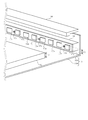
- FIG. 8 and 9 are an exploded cross-sectional perspective view and a cross-sectional view, respectively, showing the main configuration of such a conventional backlight of the edge light system.
- This backlight has a substrate (hereinafter referred to as “LED substrate”) 12 on which a plurality of LEDs 12a are mounted at a predetermined interval, a heat conductive member 14 disposed on the back surface of the LED substrate 12, and a plurality of LEDs 12a on one side.
- the chassis 11 and a rectangular frame-shaped panel frame 18 disposed on the backlight chassis 11 are configured.
- illustration of the reflective sheet 15 and the optical sheet 17 is abbreviate
- an LED 12a as a light source is arranged at a position close to one side surface of the light guide plate 16 so that light incident on the light guide plate 16 from the one side surface faces the liquid crystal panel.
- the light guide plate 16 is configured to emit light from the surface.
- one side surface of the light guide plate 16 on which the light from the LED 12a enters may be referred to as a “light incident surface”.
- the LED 12a is a point light source, if the position of the LED 12a with respect to the light guide plate 16 is shifted, the luminance in the light guide plate 16 becomes non-uniform. That is, optical unevenness occurs. Therefore, conventionally, a method of fixing the LED substrate 12 to the heat conducting member 14 using a screw 13a as shown in FIG. 8 is known.
- the LED board 12 is provided with screw holes at predetermined intervals. In FIG. 8, from the right side of the figure, between the first LED 12a and the second LED 12a, between the fourth LED 12a and the fifth LED 12a, and between the seventh LED 12a and the eighth LED 12a, respectively.
- the example in which the screw hole is provided is shown.
- the LED board 12 is fixed to the heat conducting member 14 by screwing screws 13a into the respective screw holes.
- the heat conducting member 14 is fixed to the backlight chassis 11 by means not shown (for example, screws). According to such a structure, position shift of LED12a can be prevented.
- FIGS. 10 and 11 are an exploded perspective view and a cross-sectional view, respectively, showing the main configuration of a conventional backlight using a double-sided tape 13b for fixing the LED substrate 12 and the heat conducting member 14.
- FIG. Since the configuration other than the double-sided tape 13b is the same as that of the backlight shown in FIGS. 8 and 9, the same reference numerals are used and description thereof is omitted. Even with such a configuration, the positional deviation of the LED 12a can be prevented.
- a technique for bonding the substrate and the heat conducting member using a double-sided tape is disclosed in, for example, Patent Document 1.
- Patent Document 2 a bent light source FPC (Flexible Printed Circuit: flexible printed circuit board) and a backlight chassis are bonded to each other with a double-sided tape, and the upper surface of the double-sided tape is pressed with a panel provided with a spacer. A backlight is disclosed. According to such a configuration, since the floating of the FPC is suppressed, the positional deviation of the LED 12a can be prevented.
- FPC Flexible Printed Circuit: flexible printed circuit board
- a light guide plate 16 having a thickness L1 (length in the vertical direction in FIG. 8) of 3 to 4 mm is conventionally used. Since the LED 12a used in this case has a width L2 (length in the vertical direction in FIG. 8) of about 3 mm, the width of the LED substrate 12 (length in the vertical direction in FIG. 8) also has a size corresponding thereto. Here, the size of each screw hole is about 2 mm in diameter. In this case, since the area of the screw hole with respect to the width of the LED substrate 12 is small, even if the screw 13a is used, the wiring of the LED substrate 12 is not affected.
- the ratio of the weight of the light guide plate 16 to the total weight is large.
- the width L2 of the LED 12a is about 1.5 mm.
- the light guide plate 16 can be reduced in weight by about 2.5 kg by changing the thickness L1 of the light guide plate 16 from 4 mm to 2 mm.
- the width of the LED 12 substrate is also reduced accordingly. If the size of each screw hole is about 2 mm in diameter as described above, the area of the screw hole with respect to the width of the LED substrate 12 becomes large. As a result, the use of the screw 13a increases the influence on the wiring of the LED board 12. That is, the wiring of the LED substrate 12 becomes difficult. Further, even if the mounting interval between the LEDs 12a is increased and the screws 13a are used in order to secure a wiring space, optical unevenness occurs due to the difference in reflectance between the screws 13a and the LED substrate 12.
- the LED 12 substrate is warped by the heat generated from the LED 12a, and the LED substrate 12 is removed from the heat conducting member 14. Peel off. That is, the LED substrate 12 floats from the heat conducting member 14. Thereby, since the distance between the LED 12a and the light guide plate 16 varies, optical unevenness occurs. Moreover, since the heat generated from the LED 12a is not transferred to the heat conducting member 14, this heat is concentrated on the LED 12a. As a result, the life of the LED 12a is deteriorated.
- the above-described method of adhering the LED substrate 12 and the heat conducting member 14 with the double-sided tape 13b is used.
- the LED 12 substrate is warped by the heat generated from the LED 12a, and the LED substrate 12 is lifted from the heat conducting member 14.
- the backlight described in Patent Document 2 uses an FPC for the LED substrate. Therefore, when a metal substrate is used as the LED substrate, the configuration described in Patent Document 2 cannot be employed.
- an object of the present invention is to provide a planar illumination device in which optical unevenness is suppressed and lifetime deterioration of a light emitting diode is suppressed, and a liquid crystal display device including the same.
- a first aspect of the present invention is an edge light type planar illumination device, A dish-shaped chassis including a rectangular bottom surface and a side wall surrounding the bottom surface; A substrate disposed inside the chassis along the side wall portion, and a plurality of light emitting diodes mounted on the first main surface at a predetermined interval; A light guide plate having one side face close to the plurality of light emitting diodes; A first heat conducting member disposed on a second main surface side of the substrate; A rectangular frame-like frame disposed on the chassis, On one longitudinal side surface of the substrate, first convex portions are provided at predetermined intervals, Second protrusions are provided at predetermined intervals on the other longitudinal side surface of the substrate, A first hole portion having a shape corresponding to the first convex portion is provided at a position corresponding to the first convex portion of the bottom surface portion, A second hole having a shape corresponding to the second convex portion is provided at a position corresponding to the second convex portion of the frame; The first convex portion is fitted into the
- the substrate and the first thermal conductive member are fixed to each other by an adhesive member having thermal conductivity.
- the adhesive member has a cushioning property
- the first hole portion is larger in the vertical direction of the first main surface than the first convex portion facing the first hole portion
- the second hole portion is larger in a direction perpendicular to the first main surface than the second convex portion facing the second hole portion.
- the substrate and the first heat conducting member are fixed to each other by screws.
- the chassis is made of resin.
- a sixth aspect of the present invention is the fifth aspect of the present invention, A second heat conductive member disposed on the outer surface of the bottom surface portion and having a higher thermal conductivity than the chassis; A part of the second heat conducting member is in contact with the first convex portion.
- a seventh aspect of the present invention is a liquid crystal display device, LCD panel, It is arrange
- the planar illuminating device which concerns on either from the 1st aspect of this invention which irradiates light to the said liquid crystal panel is provided, It is characterized by the above-mentioned.
- the first convex portion and the second convex portion are fitted into the first hole portion and the second hole portion, respectively, thereby fixing the substrate on which the plurality of light emitting diodes are mounted.
- the floating of the substrate from the first heat conducting member is more reliably prevented. Thereby, the effect of suppressing optical unevenness can be further enhanced.
- the position of the substrate can be changed in the direction perpendicular to the first main surface. Accordingly, when the light guide plate is thermally expanded, the light emitting diode is hardly damaged, the substrate is not easily cracked, and the like.
- the floating of the substrate from the first heat conducting member is more reliably prevented.
- the effect of suppressing optical unevenness can be further enhanced. Therefore, the distance between the light guide plate and the light emitting diode can be made smaller than before. Thereby, the incident efficiency of the light from the light emitting diode to the one side surface of the light guide plate can be increased as compared with the conventional case.
- the fifth aspect of the present invention it is possible to reduce the weight of the backlight by using a resin as the chassis material.
- the heat generated in the light emitting diode is sufficiently dissipated to the outside.
- the seventh aspect of the present invention even when the liquid crystal display device is reduced in thickness and weight, optical unevenness can be suppressed and at the same time deterioration of the life of the light emitting diode can be suppressed.
- (B) is sectional drawing at the time of thermal expansion. It is sectional drawing which shows the reference example of a backlight provided with the backlight chassis which consists of resin. It is sectional drawing which shows the principal part structure of the backlight which concerns on the 3rd Embodiment of this invention. It is a disassembled cross-sectional perspective view which shows the principal part structure of the conventional backlight. It is sectional drawing which shows the principal part structure of the conventional backlight. It is a disassembled cross-sectional perspective view which shows the principal part structure of the conventional backlight. It is sectional drawing which shows the principal part structure of the conventional backlight.
- FIG. 1 is an exploded perspective view showing a configuration of a liquid crystal display device including a backlight (planar illumination device) according to the first embodiment of the present invention.
- the liquid crystal display device 100 includes the backlight 10, the liquid crystal panel 20, and the bezel 30 according to the present embodiment.
- the configuration of the backlight 10 will be described in detail later.
- the liquid crystal panel 20 is composed of a pair of electrode substrates that sandwich a liquid crystal layer, and a polarizing plate is attached to the outer surface of each electrode substrate.
- One of the pair of electrode substrates is an active matrix substrate called a TFT (Thin Film Transistor) substrate.
- TFT substrate a plurality of data signal lines and a plurality of scanning signal lines are formed in a lattice shape on an insulating substrate such as a glass substrate so as to intersect each other.
- a plurality of pixel circuits are formed corresponding to the intersections of the plurality of data signal lines and the plurality of scanning signal lines, respectively.
- the other of the pair of electrode substrates is called a counter substrate, and a common electrode and an alignment film are sequentially stacked over an entire surface of an insulating substrate such as glass.
- the bezel 30 is a rectangular frame-shaped member for holding the liquid crystal panel 20, and is made of a metal material such as aluminum.
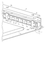
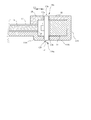
- FIGS. 2 and 3 are an exploded cross-sectional perspective view and a cross-sectional view, respectively, showing the main configuration of the backlight 10 according to the present embodiment.
- the backlight 10 irradiates light from the back surface of the liquid crystal panel 20 (the surface opposite to the surface to be viewed), thereby giving the display of the liquid crystal panel 20 a predetermined luminance.
- the backlight 10 includes a backlight chassis 11 as a dish-shaped chassis, an LED substrate 12, a double-sided tape 13b as an adhesive member, and a heat conducting member 14 as a first heat conducting member.
- the reflection sheet 15, the light guide plate 16, the optical sheet 17, and the rectangular frame-shaped panel frame 18 are included.
- the backlight chassis 11 is made of an aluminum material or an electrogalvanized steel plate. As shown in FIGS. 1 to 3, the backlight chassis 11 includes a rectangular bottom surface portion 11B and a side wall portion 11S surrounding the bottom surface portion 11B. A plurality of chassis hole portions 11Ba as first hole portions are provided in the bottom surface portion 11B of the backlight chassis 11. The details of the chassis hole 11Ba will be described later. As shown in FIG. 3, in the bottom surface portion 11 ⁇ / b> B, the portion where the LED substrate 12, the double-sided tape 13 b, and the heat conducting member 14 are disposed is preferably formed to be slightly recessed from the other portions.
- the backlight chassis 11 is a member for holding the rigidity of the liquid crystal display device 100 and holding the above-described members such as the LED substrate 12 inside.
- the backlight chassis 11 also functions as a heat radiating member for radiating heat generated from the LEDs 12a.
- the LED substrate 12 is a metal substrate such as an aluminum substrate from the viewpoint of heat dissipation and strength. As shown in FIGS. 1 to 3, the LED substrate 12 is disposed inside the backlight chassis 11 along the side wall portion 11S of the backlight chassis 11. A plurality of LEDs 12a as light sources are mounted on the front surface as the first main surface of the LED substrate 12 at a predetermined interval. A part of the LED substrate 12 is formed in a convex shape. That is, on the long side surface of the LED substrate 12 facing the bottom surface portion 11B of the backlight chassis 11 (hereinafter referred to as “lower long side surface”), a lower convex portion 12b as a convex first convex portion is provided at a predetermined interval. A plurality are provided.
- a plurality of upper convex portions 12c as convex second convex portions are provided at predetermined intervals on the longitudinal side surface (hereinafter referred to as “upper longitudinal side surface”) of the LED substrate 12 facing the panel frame 18. . Details of the lower convex portion 12b and the upper convex portion 12c will be described later.
- the double-sided tape 13b is a double-sided adhesive tape having thermal conductivity. As shown in FIGS. 1 to 3, the double-sided tape 13b is disposed on the back surface (surface opposite to the front surface) as the second main surface of the LED substrate 12. The LED substrate 12 and the heat conducting member 14 are fixed to each other by the double-sided tape 13b.
- the heat conducting member 14 is made of an aluminum material or the like.
- the heat conducting member 14 is a member for absorbing heat generated from the LED 12a and dissipating it to the backlight chassis 11 or the like. As shown in FIGS. 1 to 3, the heat conducting member 14 is disposed on the back side of the LED substrate 12 via a double-sided tape 13b.
- the heat conducting member 14 is fixed to the backlight chassis 11 by means (not shown) such as screws.
- the light guide plate 16 is made of a highly transparent resin such as acrylic and is formed in a flat plate shape. As shown in FIGS. 1 to 3, the light guide plate 16 is disposed so as to face the back surface of the liquid crystal panel 20 and one side surface (light incident surface) thereof is close to the plurality of LEDs 12a. It is desirable that the thickness L1 (length in the vertical direction in FIG. 2) of the light guide plate 16 and the width L2 (length in the vertical direction in FIG. 2) of each LED 12a are substantially equal to each other. Further, from the viewpoint of preventing the LED 12a from being damaged by the thermal expansion of the light guide plate 16 and the cracking of the LED substrate 12, it is desirable to provide a slight gap between the light incident surface of the light guide plate 16 and the LED 12a.
- this gap is referred to as “light guide plate-LED distance L3”. If the distance L3 between the light guide plate and the LED is too large, the incident efficiency from the LED 12a to the light incident surface of the light guide plate 16 is deteriorated. On the other hand, if the distance L3 between the light guide plate and the LED is too small, the LED 12a may be damaged or the LED substrate 12 may be cracked due to thermal expansion of the light guide plate 16, as described above. Therefore, in this embodiment, the distance L3 between the light guide plate and the LED is set to 1 mm, for example.
- a reflective sheet 15 is disposed on the back side of the light guide plate 16 (the side facing the bottom surface portion 11B of the backlight chassis 11).
- the reflection sheet 15 reflects light leaking from the back side of the light guide plate 16 to the front side (side facing the liquid crystal panel 20).
- An optical sheet 17 composed of a lens sheet, a diffusion sheet or the like is disposed on the front side of the light guide plate 16 (the side facing the liquid crystal panel 20).
- the optical sheet 17 condenses and diffuses light emitted from the front side of the light guide plate 16 and efficiently emits the light to the liquid crystal panel 20.
- the panel frame 18 is made of a resin such as polycarbonate. As shown in FIGS. 1 to 3, the panel frame 18 is disposed on the backlight chassis 11 so as to cover the ends of the LED substrate 12, the double-sided tape 13b, the heat conducting member 14, and the optical sheet 17.
- the panel frame 18 is a member for holding the liquid crystal panel 20 while keeping the distance therebetween so that the optical sheet 17 and the liquid crystal panel 20 do not come into contact with each other.
- the panel frame 18 is provided with a plurality of frame hole portions 18a as second hole portions. The details of the frame hole 18a will be described later.
- the heat generated from the LED 12a serving as the light source is first transmitted to the LED substrate 12, and then transmitted to the double-sided tape 13b, the heat conducting member 14, and the backlight chassis 11 in this order to dissipate heat. Further, in the present embodiment, the heat transmitted to the LED substrate 12 is directly radiated to the outside from the lower convex portion 12b. Therefore, in this embodiment, the heat generated from the LED 12a can be radiated more efficiently than in the past. Such a heat dissipation effect increases as the number of the lower convex portions 12b increases.
- each chassis hole portion 11Ba is formed in a shape corresponding to the corresponding lower convex portion 12b. That is, each chassis hole part 11Ba is formed in the position and shape which can engage
- the upper convex portion 12a is provided at a position corresponding to each lower convex portion 12b in the upper longitudinal side surface.
- the frame hole 18a is provided in the panel frame 18 at a position corresponding to each upper protrusion 12c.
- Each frame hole 18a is formed in a shape corresponding to the corresponding upper convex portion 12c. That is, each frame hole 18a is formed in a position and a shape in which the corresponding upper projection 12c can be fitted.
- the chassis hole 11Ba is formed slightly larger in the vertical direction (lateral direction in FIG. 3) of the front surface of the LED board 12 than the lower convex part 12b corresponding to the chassis hole 11Ba.
- the frame hole 18 a is formed to be slightly larger in the vertical direction on the front surface of the LED substrate 12 than the upper convex portion 12 c corresponding to the frame hole 18.
- Each lower convex portion 12b is fitted into the corresponding chassis hole portion 11Ba.
- Each upper convex portion 12c is fitted into the corresponding frame hole portion 18a.
- the height of the lower convex portion 12b (vertical length in FIG. 3) and the height of the upper convex portion 12c (vertical length in FIG. 3) are respectively set.
- the depth of the chassis hole portion 11Ba (the thickness of the bottom surface portion 11B of the backlight chassis 11) and the depth of the frame hole portion 18a (the thickness of the panel frame 18) are the same. It is not limited.
- the height of the lower convex portion 12b and the height of the upper convex portion 12c may be larger than the depth of the chassis hole portion 11Ba and the depth of the frame hole portion 18a, respectively.
- portions protruding from the chassis hole portion 11Ba and the frame hole portion 18a may be claw-shaped. Further, the height of the lower convex portion 12b and the height of the upper convex portion 12c may be smaller than the depth of the chassis hole portion 11Ba and the depth of the frame hole portion 18a, respectively.
- the number of the lower protrusions 12b and the number of the upper protrusions 12c are the same, but the present invention is not limited to this.
- the number of the lower protrusions 12b and the number of the upper protrusions 12c may be different from each other (the same applies to modified examples described later).
- the number of chassis hole portions 11Ba and the number of frame hole portions 18a are different from each other.
- each of the lower convex portions 12b (the size in the vertical direction of the front surface of the LED substrate 12 or the direction perpendicular thereto) and the size of the chassis hole portion 11Ba facing this need only correspond to each other. Therefore, the sizes of the plurality of lower convex portions 12b may be different from each other. Similarly, since the size of each upper convex portion 12c and the size of the frame hole portion 18a opposite to each other need only correspond to each other, the sizes of the plurality of upper convex portions 12c may be different from each other.
- each lower side convex part 12b and each upper side convex part 12c are formed as a part of LED board 12,
- This invention is not limited to this.
- each lower convex part 12b and each upper convex part 12c which are members different from this may be joined to the LED substrate 12.
- the LED substrate 12 is fixed by fitting the lower convex portion 12b and the upper convex portion 12c of the LED substrate 12 into the chassis hole portion 11Ba and the frame hole portion 18a, respectively. Therefore, even if heat is generated by driving the LED 12a, the warpage of the LED substrate 12 is suppressed. Therefore, the LED substrate 12 is prevented from floating from the heat conducting member 14. Thereby, optical unevenness can be suppressed. Furthermore, at the same time, the life deterioration of the LED 12a can be suppressed.
- This embodiment is suitable for a thin and light backlight.
- the LED substrate 12 and the heat conducting member 14 are fixed to each other by the double-sided tape 13b.
- the double-sided tape 13b is not an essential configuration.
- the double-sided tape 13b is not used, for example, by providing a large number of lower convex portions 12b and upper convex portions 12c, the same effects as in the present embodiment can be achieved.
- FIG. 4 is an exploded cross-sectional perspective view showing the main configuration of the backlight 10 according to a modification of the present embodiment.
- a screw 13a is used as a fixing means for the LED substrate 12 and the heat conducting member 14 instead of the double-sided tape 13b.
- the LED board 12 is provided with a screw hole at an intermediate position between the lower convex portions 12b adjacent to each other (the same applies to the upper convex portion 12c).
- the LED board 12 is fixed to the heat conducting member 14 by screwing screws 13a into the respective screw holes.
- the backlight 10 according to the present modification reduces the number of screws 13a used in the conventional backlight shown in FIGS. 8 and 9 described above, and the lower convex portion 12b and the upper projection according to the reduced amount.
- the protrusion 12c, the chassis hole 11Ba, and the frame hole 18a are provided. Each lower convex portion 12b is fitted into the corresponding chassis hole portion 11Ba.
- each upper side convex part 12c is engage
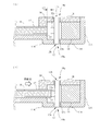
- FIG. 5A is a cross-sectional view showing a main configuration of the backlight 10 according to the present embodiment when the light guide plate 16 is not thermally expanded (hereinafter referred to as “normal time”).
- FIG. 5B is a cross-sectional view showing a main configuration of the backlight 10 according to the present embodiment when the light guide plate 16 is thermally expanded (hereinafter referred to as “thermal expansion”).
- thermal expansion a main configuration of the backlight 10 according to the present embodiment when the light guide plate 16 is thermally expanded
- the backlight 10 according to the present embodiment has the same configuration as the backlight 10 according to the first embodiment except that a double-sided tape 13b having a cushioning property is used.
- a double-sided tape 13b what applied the adhesive material to both surfaces of the foam which consists of resin with high heat conductivity, for example can be used.
- the cushioning property of the double-sided tape 13b is not too high.
- the chassis hole portion 11Ba has a vertical direction (see FIG. 5 (FIG. 5 (B)) that is lower than the lower convex portion 12b corresponding to the chassis hole portion 11Ba. A) and slightly larger in the horizontal direction in FIG.
- the frame hole 18 a is formed to be slightly larger in the vertical direction on the front surface of the LED substrate 12 than the upper convex portion 12 c corresponding to the frame hole 18.
- Each lower convex portion 12b is fitted into the corresponding chassis hole portion 11Ba.
- Each upper convex portion 12c is fitted into the corresponding frame hole portion 18a.
- a predetermined distance L3 between the light guide plate and the LED (for example, about 1 mm) is normally maintained.
- the light incident surface of the light guide plate 16 contacts the LED 12a during thermal expansion. The thermal expansion of the light guide plate 16 is caused by an increase in ambient temperature.
- the chassis hole portion 11Ba is formed slightly larger in the vertical direction of the front surface of the LED board 12 than the lower convex portion 12b corresponding to the chassis hole portion 11Ba, and the frame hole portion 18a is formed in the frame.
- a double-sided tape 13b having a cushioning property is disposed on the back surface of the LED substrate 12 while being slightly larger in the vertical direction of the front surface of the LED substrate 12 than the upper convex portion 12c corresponding to the hole 18. Therefore, as shown in FIG. 5B, even if the light incident surface of the light guide plate 16 contacts the LED 12a during thermal expansion, the position of the LED substrate 12 can be changed in the vertical direction of the front surface of the LED substrate 12. ing.
- the conventional light guide plate-LED substrate distance L3 in the conventional backlight shown in FIGS. 10 and 11 and the backlight 10 according to the present embodiment are equal to each other. Since the position of the LED substrate 12 does not change in the conventional backlight, when the light incident surface of the light guide plate 16 contacts the LED 12a during thermal expansion, the LED 12a and the LED substrate 12 are in contact with the LED 12 in the vertical direction (thermal conducting member). 14 side) load. Therefore, the LED 12a may be damaged or the LED substrate 12 may be cracked.
- the position of the LED substrate 12 can be changed in the vertical direction of the front surface of the LED substrate 12 as described above. Even if it contacts the LED 12a, the LED 12a is hardly damaged, the LED substrate 12 is not easily cracked, and the like. In other words, in the present embodiment, the distance L3 between the light guide plate and the LED can be made smaller than in the prior art.
- the position of the LED substrate 12 can be changed in the vertical direction of the front surface of the LED substrate 12, so that the LED 12a is hardly damaged or the LED substrate 12 is not easily cracked during thermal expansion. Therefore, the distance L3 between the light guide plate and the LED can be made smaller than before. Thereby, the incident efficiency of the light from the LED 12a to the light incident surface of the light guide plate 16 can be improved as compared with the conventional case.
- the backlight chassis 11 should also function as a heat radiating member for radiating the heat generated from the LEDs 12a.
- the resin is more thermally conductive than an aluminum material or an electrogalvanized steel sheet. Low. Therefore, the backlight chassis 11 made of resin cannot sufficiently dissipate the heat generated from the LEDs 12a as compared with the backlight chassis 11 made of aluminum material, electrogalvanized steel plate or the like.
- FIG. 6 shows a conventional backlight shown in FIGS. 10 and 11, in which the material of the backlight chassis 11 is replaced with a resin instead of an aluminum material and the like, and the LED board 12 on which the LEDs 12a are mounted and the bottom surface of the backlight chassis 11.
- FIG. 6 shows a conventional backlight shown in FIGS. 10 and 11, in which the material of the backlight chassis 11 is replaced with a resin instead of an aluminum material and the like, and the LED board 12 on which the LEDs 12a are mounted and the bottom surface of the backlight chassis 11.
- the backlight according to this reference example has the same configuration as the conventional backlight shown in FIGS. 10 and 11 except that the backlight chassis 11 is made of resin and the graphite sheet 19 is provided. .
- the graphite sheet 19 is disposed between the LED substrate 12, the double-sided tape 13 b, the heat conducting member 14, and the reflective sheet 15 and the bottom surface portion 11 ⁇ / b> B of the backlight chassis 11. Is provided.
- the heat generated from the LED 12a is first transmitted to the LED substrate 12.
- the backlight chassis 11 is made of a resin having low thermal conductivity, the heat transmitted to the LED board 12 is not easily radiated from the backlight chassis 11 after being transmitted in the order of the double-sided tape 13b and the heat conductive member 14. Become.
- the graphite sheet 19 is in contact with the lower longitudinal side surface of the LED substrate 12, the heat transmitted to the LED substrate 12 is transmitted to the graphite sheet 19.
- the thermal conductivity of the graphite sheet 19 is superior in the plane direction (lateral direction in FIG. 6) than in the thickness direction (vertical direction in FIG. 6). Furthermore, the thermal conductivity of the backlight chassis 11 made of resin is low as described above. Therefore, in the reference example shown in FIG. 6, the heat generated in the LED 12 a is not easily dissipated to the outside of the backlight, and this heat is transmitted to the reflective sheet 15, the light guide plate 16, and the optical sheet 17 through the graphite sheet 19. It is transmitted. As a result, the reflection sheet 15, the light guide plate 16, and the optical sheet 17 are warped and bent.
- the material of the backlight chassis 11 is replaced with an aluminum material or the like, and an LED substrate on which an LED 12a is further mounted. The same problem occurs when a graphite sheet is provided between 12 and the bottom surface portion 11B of the backlight chassis 11.
- the backlight 10 according to the third embodiment of the present invention described below even if a resin is used as the material of the backlight chassis 11, the heat generated by the LED 12a is sufficiently dissipated to the outside.
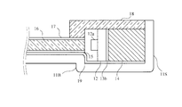
- FIG. 7 is a cross-sectional view showing a main configuration of the backlight 10 according to the present embodiment.
- the same referential mark is attached
- the backlight 10 according to the present embodiment is the same as the backlight 10 according to the first embodiment except that the backlight chassis 11 is made of resin and further includes a graphite sheet 19 as a second heat conducting member. It is the composition.
- the outer surface of the bottom surface portion 11B of the backlight chassis 11 covers the chassis hole portion 11Ba and touches the lower convex portion 12b of the LED substrate 12.
- a graphite sheet 19 is arranged.
- the thermal conductivity of the graphite sheet 19 is higher than the thermal conductivity of the backlight chassis 11 made of resin.
- the heat generated in the LED 12a is first transmitted to the LED substrate 12, and then transmitted to the graphite sheet 19 from the lower convex portion 12b.
- the heat transferred to the graphite sheet 19 spreads in the plane direction of the graphite sheet 19 (lateral direction in FIG. 7) and is radiated to the outside.
- the thermal conductivity of the backlight chassis 11 is low, the heat transmitted to the graphite sheet 19 is not easily transmitted to the reflection sheet 15, the light guide plate 16, and the optical sheet 17. Therefore, it is possible to prevent the reflection sheet 15, the light guide plate 16, and the optical sheet 17 from being warped or bent.
- planar lighting device according to the present invention has been described by way of example as the backlight of a liquid crystal display device, but the present invention is not limited to this.
- the planar lighting device according to the present invention may be used alone as a lighting device.
- the present invention it is possible to provide a planar illumination device in which optical unevenness is suppressed and lifetime deterioration of a light emitting diode is suppressed, and a liquid crystal display device including the same.
- the present invention can be applied to an edge light type planar illumination device using an LED as a light source.
Landscapes
- Physics & Mathematics (AREA)
- General Physics & Mathematics (AREA)
- Optics & Photonics (AREA)
- Liquid Crystal (AREA)
- Planar Illumination Modules (AREA)
Abstract
光学的なムラが抑制されると共に、発光ダイオードの寿命劣化が抑制された面状照明装置およびそれを備えた液晶表示装置を提供する。 複数のLED(12a)が実装されたLED基板(12)とその背面に配置された熱伝導部材(14)とは、両面テープ(13b)により互いに固定される。LED基板(12)の下側長手側面には複数の下側凸部(12b)が、上側長手側面には複数の上側凸部(12c)が設けられる。バックライトシャーシ(11)の底面部(11B)のうち、各下側凸部(12b)に対応する位置にはシャーシ穴部(11Ba)が設けられる。パネルフレーム(18)のうち、各上側凸部(12c)に対応する位置にはフレーム穴部(18a)が設けられる。各下側凸部(12b)は対応するシャーシ穴部(11Ba)に嵌め込まれる。各上側凸部(12c)は対応するフレーム穴部(18a)に嵌め込まれる。
Description
本発明は、エッジライト方式の面状照明装置およびそれを備える液晶表示装置に関し、特に、LED(Light Emitting Diode:発光ダイオード)を光源として用いたエッジライト方式の面状照明装置および当該面状照明装置をバックライトとして備える液晶表示装置に関する。
従来から、液晶パネルを用いた液晶表示装置が知られている。この液晶表示装置では、液晶パネルの背面に配置されたバックライトから、液晶パネルに光を照射することにより画像表示が行われる。バックライトの方式として、導光板を用いたエッジライト方式(サイドライト方式ともいう)が広く採用されている。また近年、このエッジライト方式のバックライトの光源として、小型で低消費電力駆動が可能なLEDが用いられている。
図8および図9はそれぞれ、このようなエッジライト方式の従来のバックライトの要部構成を示す分解断面斜視図および断面図である。このバックライトは、複数のLED12aが所定間隔に実装された基板(以下、「LED基板」という)12と、LED基板12の背面に配置された熱伝導部材14と、複数のLED12aに一側面が近接した導光板16と、導光板16の背面側に配置された反射シート15と、導光板16の前面側に配置された光学シート17と、これらの部材を内部に保持する皿状のバックライトシャーシ11と、バックライトシャーシ11上に配置された矩形枠状のパネルフレーム18とにより構成されている。なお、図8では、反射シート15および光学シート17の図示を便宜上省略している。
このようなエッジライト方式のバックライトは、導光板16の一側面に近接した位置に光源としてのLED12aを配置することにより、当該一側面から導光板16に入射した光を液晶パネルに対向する側の導光板16の面から出射するように構成されている。以下の説明では、LED12aからの光が入射する導光板16の一側面を「光入射面」ということがある。
LED12aは点光源であるため、導光板16に対するLED12aの位置がずれると、導光板16内での輝度が不均一になってしまう。すなわち、光学的なムラが生じてしまう。そこで従来、図8に示すような、ネジ13aを用いてLED基板12を熱伝導部材14に固定する方法が知られている。
LED基板12には所定間隔でネジ穴が設けられている。図8では、図の右側から1番目のLED12aと2番目のLED12aとの間、4番目のLED12aと5番目のLED12aとの間、および7番目のLED12aと8番目のLED12aとの間のそれぞれにネジ穴が設けられている例を示している。各ネジ穴にネジ13aを螺合することにより、LED基板12が熱伝導部材14に固定されている。なお、熱伝導部材14は、図示しない手段(例えばネジ)によりバックライトシャーシ11に固定されている。このような構成によれば、LED12aの位置ずれを防止することができる。
また、ネジ13aに代えて、LED基板12と熱伝導部材14とを両面テープ13bにより互いに固定する方法が知られている。図10および図11はそれぞれ、LED基板12と熱伝導部材14との固定に両面テープ13bを用いた従来のバックライトの要部構成を示す分解斜視図および断面図である。なお、両面テープ13b以外の構成は図8および図9に示すバックライトと同様であるので、同一の参照符号を付して説明を省略する。このような構成によっても、LED12aの位置ずれを防止することができる。このように基板と熱伝導部材を両面テープを用いて接着する技術は、例えば特許文献1に開示されている。
また、特許文献2には、屈曲させた光源用FPC(Flexible Printed Circuit:フレキシブルプリント基板)とバックライトシャーシとを両面テープで接着すると共に、この両面テープの上面を、スペーサを配したパネルで押さえたバックライトが開示されている。このような構成によれば、FPCの浮きが抑制されるので、LED12aの位置ずれを防止することができる。
大型バックライトでは、厚さL1(図8における縦方向の長さ)が3~4mmの導光板16が従来用いられている。この場合に用いられるLED12aの幅L2(図8における縦方向の長さ)は3mm程度となるので、LED基板12の幅(図8における縦方向の長さ)もこれに応じた大きさとなる。ここで、各ネジ穴のサイズは直径2mm程度である。この場合、LED基板12の幅に対するネジ穴の面積が小さいので、ネジ13aを用いてもLED基板12の配線に影響を与えない。
大型バックライトでは、全体の重量の中で導光板16の重量の占める割合が大きい。バックライトの薄型化および軽量化を図るために導光板16の厚さL1を1.5~2.0mmに変更した場合、LED12aの幅L2は1.5mm程度となる。なお、例えば60型のバックライトでは、導光板16の厚さL1を4mmから2mmに変更することにより約2.5kgの軽量化を図ることができる。
LED12aの幅L2を1.5mmまで小さくすると、LED12基板の幅もこれに合わせて小さくなる。各ネジ穴のサイズが上述のような直径2mm程度であるとすると、LED基板12の幅に対するネジ穴の面積が大きくなる。その結果、ネジ13aの使用によりLED基板12の配線に与える影響が大きくなる。すなわち、LED基板12の配線が困難になる。また、配線スペースを確保するためにLED12aの実装間隔を広くしてネジ13aを用いたとしても、ネジ13aとLED基板12との反射率の違いにより光学的なムラが生じる。さらに、この反射率の違いの影響を低減するために、使用するネジ13aの数を削減した場合には、LED12aから発生した熱によりLED12基板に反りが生じ、LED基板12が熱伝導部材14から剥がれる。すなわち、LED基板12が熱伝導部材14から浮く。これにより、LED12aと導光板16との間の距離が変動するので、光学的なムラが生じる。また、LED12aから発生した熱が熱伝導部材14に伝達されなくなるので、この熱がLED12aに集中する。その結果、LED12aの寿命が劣化する。
そこで、薄型化・軽量化を図るために導光板16の厚さL1を小さくしたバックライトでは、LED基板12と熱伝導部材14とを両面テープ13bにより接着する上述の方法が用いられる。しかし、この場合にも上述の少ない数のネジ13aを使用した場合と同様に、LED12aから発生した熱によりLED12基板に反りが生じ、LED基板12が熱伝導部材14から浮く。
すなわち、薄型化・軽量化されたバックライトでは、ネジ13aまたは両面テープ13bのいずれを使用しても、光学的なムラが生じ、また、LED12aの寿命が劣化する。
また、特許文献2に記載のバックライトはLED基板にFPCを用いたものである。そのため、LED基板として金属基板を用いる場合には特許文献2に記載の構成を採用することができない。
そこで、本発明は、光学的なムラが抑制されると共に、発光ダイオードの寿命劣化が抑制された面状照明装置およびそれを備えた液晶表示装置を提供することを目的とする。
本発明の第1の局面は、エッジライト方式の面状照明装置であって、
矩形状の底面部および当該底面部を取り囲む側壁部を含む皿状のシャーシと、
前記側壁部に沿って前記シャーシ内部に配置され、複数の発光ダイオードが所定間隔に第1主面に実装された基板と、
前記複数の発光ダイオードに一側面が近接した導光板と、
前記基板における第2主面側に配置された第1熱伝導部材と、
前記シャーシ上に配置された矩形枠状のフレームとを備え、
前記基板の一方の長手側面に、所定間隔に第1凸部が設けられ、
前記基板の他方の長手側面に、所定間隔に第2凸部が設けられ、
前記底面部の前記第1凸部に対応する位置に、当該第1凸部に対応した形状の第1穴部が設けられ、
前記フレームの前記第2凸部に対応する位置に、当該第2凸部に対応した形状の第2穴部が設けられ、
前記第1凸部は、当該第1凸部に対応する前記第1穴部に嵌め込まれ、
前記第2凸部は、当該第2凸部に対応する前記第2穴部に嵌め込まれていることを特徴とする。
矩形状の底面部および当該底面部を取り囲む側壁部を含む皿状のシャーシと、
前記側壁部に沿って前記シャーシ内部に配置され、複数の発光ダイオードが所定間隔に第1主面に実装された基板と、
前記複数の発光ダイオードに一側面が近接した導光板と、
前記基板における第2主面側に配置された第1熱伝導部材と、
前記シャーシ上に配置された矩形枠状のフレームとを備え、
前記基板の一方の長手側面に、所定間隔に第1凸部が設けられ、
前記基板の他方の長手側面に、所定間隔に第2凸部が設けられ、
前記底面部の前記第1凸部に対応する位置に、当該第1凸部に対応した形状の第1穴部が設けられ、
前記フレームの前記第2凸部に対応する位置に、当該第2凸部に対応した形状の第2穴部が設けられ、
前記第1凸部は、当該第1凸部に対応する前記第1穴部に嵌め込まれ、
前記第2凸部は、当該第2凸部に対応する前記第2穴部に嵌め込まれていることを特徴とする。
本発明の第2の局面は、本発明の第1の局面において、
前記基板と前記第1熱伝導部材とは、熱伝導性を有する接着部材により互いに固定されていることを特徴とする。
前記基板と前記第1熱伝導部材とは、熱伝導性を有する接着部材により互いに固定されていることを特徴とする。
本発明の第3の局面は、本発明の第2の局面において、
前記接着部材はクッション性を有し、
前記第1穴部は、当該第1穴部に対向する前記第1凸部よりも前記第1主面の垂直方向に大きく、
前記第2穴部は、当該第2穴部に対向する前記第2凸部よりも前記第1主面の垂直方向に大きいことを特徴とする。
前記接着部材はクッション性を有し、
前記第1穴部は、当該第1穴部に対向する前記第1凸部よりも前記第1主面の垂直方向に大きく、
前記第2穴部は、当該第2穴部に対向する前記第2凸部よりも前記第1主面の垂直方向に大きいことを特徴とする。
本発明の第4の局面は、本発明の第1の局面において、
前記基板と前記第1熱伝導部材とはネジにより互いに固定されていることを特徴とする。
前記基板と前記第1熱伝導部材とはネジにより互いに固定されていることを特徴とする。
本発明の第5の局面は、本発明の第1の局面において、
前記シャーシは樹脂からなることを特徴とする。
前記シャーシは樹脂からなることを特徴とする。
本発明の第6の局面は、本発明の第5の局面において、
前記底面部の外面に配置された、前記シャーシよりも熱伝導性は高い第2熱伝導部材をさらに備え、
前記第2熱伝導部材の一部は前記第1凸部に接することを特徴とする。
前記底面部の外面に配置された、前記シャーシよりも熱伝導性は高い第2熱伝導部材をさらに備え、
前記第2熱伝導部材の一部は前記第1凸部に接することを特徴とする。
本発明の第7の局面は、液晶表示装置であって、
液晶パネルと、
前記液晶パネルの背面側に配置され、当該液晶パネルに光を照射する本発明の第1の局面から第6の局面までのいずれかに係る面状照明装置とを備えることを特徴とする。
液晶パネルと、
前記液晶パネルの背面側に配置され、当該液晶パネルに光を照射する本発明の第1の局面から第6の局面までのいずれかに係る面状照明装置とを備えることを特徴とする。
本発明の第1の局面によれば、第1凸部および第2凸部がそれぞれ、第1穴部および第2穴部に嵌め込まれることにより、複数の発光ダイオードが実装された基板が固定される。そのため、発光ダイオードの駆動により熱が生じても、基板の反りが抑制される。したがって、第1熱伝導部材からの基板の浮きが防止される。これにより、光学的なムラを抑制することができる。さらに、これと同時に発光ダイオードの寿命劣化を抑制することができる。
本発明の第2の局面によれば、第1熱伝導部材からの基板の浮きがより確実に防止される。これにより、光学的なムラの抑制効果をより高めることができる。
本発明の第3の局面によれば、基板の位置が第1主面の垂直方向に変動可能となる。これにより、導光板が熱膨張したときに、発光ダイオードの損傷や基板の割れ等が生じにくくなる。
本発明の第4の局面によれば、第1熱伝導部材からの基板の浮きがより確実に防止される。これにより、光学的なムラの抑制効果をより高めることができる。したがって、導光板と発光ダイオードとの間の距離を従来よりも小さくすることができる。これにより、発光ダイオードから導光板の一側面への光の入射効率を従来よりも高めることができる。
本発明の第5の局面によれば、シャーシの材料として樹脂を用いることにより、バックライトを軽量化することができる。
本発明の第6の局面によれば、面状照明装置を軽量化した場合でも、発光ダイオードで発生した熱が十分に外部に放熱される。
本発明の第7の局面によれば、液晶表示装置を薄型化・軽量化した場合であっても、光学的なムラを抑制すると同時に、発光ダイオードの寿命劣化を抑制することができる。
以下、本発明の実施形態について、添付図面を参照しながら説明する。
<1.第1の実施形態>
<1.1 液晶表示装置の構成>
図1は、本発明の第1の実施形態に係るバックライト(面状照明装置)を備えた液晶表示装置の構成を示す分解斜視図である。この液晶表示装置100は、本実施形態に係るバックライト10、液晶パネル20、およびベゼル30により構成されている。バックライト10の構成については、後で詳しく説明する。
<1.1 液晶表示装置の構成>
図1は、本発明の第1の実施形態に係るバックライト(面状照明装置)を備えた液晶表示装置の構成を示す分解斜視図である。この液晶表示装置100は、本実施形態に係るバックライト10、液晶パネル20、およびベゼル30により構成されている。バックライト10の構成については、後で詳しく説明する。
液晶パネル20は、液晶層を挟持する1対の電極基板からなり、各電極基板の外表面には偏光板が貼り付けられている。上記1対の電極基板の一方はTFT(Thin Film Transistor)基板と呼ばれるアクティブマトリクス型の基板である。このTFT基板では、ガラス基板等の絶縁性基板上に、複数のデータ信号線と複数の走査信号線とが互いに交差するように格子状に形成されている。また、複数のデータ信号線と複数の走査信号線との交差点にそれぞれ対応して複数の画素回路が形成されている。上記1対の電極基板の他方は対向基板と呼ばれ、ガラス等の絶縁性基板上に、全面にわたって共通電極、配向膜が順次積層されている。
ベゼル30は液晶パネル20を保持するための矩形枠状の部材であり、アルミ等の金属素材からなる。
<1.2 バックライトの構成>
本実施形態に係るバックライト10について、図1~図3を参照しつつ説明する。図2および図3はそれぞれ、本実施形態に係るバックライト10の要部構成を示す分解断面斜視図および断面図である。
本実施形態に係るバックライト10について、図1~図3を参照しつつ説明する。図2および図3はそれぞれ、本実施形態に係るバックライト10の要部構成を示す分解断面斜視図および断面図である。
本実施形態に係るバックライト10は、液晶パネル20の背面(視認される面と反対側の面)から光を照射することにより、液晶パネル20の表示に所定の輝度を持たせる。図1~図3に示すように、このバックライト10は、皿状のシャーシとしてのバックライトシャーシ11、LED基板12、接着部材としての両面テープ13b、第1熱伝導部材としての熱伝導部材14、反射シート15、導光板16、光学シート17と、矩形枠状のパネルフレーム18とにより構成されている。
バックライトシャーシ11はアルミ材または電気亜鉛メッキ鋼板等からなる。図1~図3に示すように、このバックライトシャーシ11は、矩形状の底面部11Bおよび当該底面部11Bを取り囲む側壁部11Sにより構成されている。このバックライトシャーシ11の底面部11Bには第1穴部としてのシャーシ穴部11Baが複数個設けられている。なお、シャーシ穴部11Baの詳細は後述する。図3に示すように、底面部11Bのうち、LED基板12、両面テープ13b、および熱伝導部材14が配置される部分は、他の部分よりも少し凹ませて形成されていることが望ましい。バックライトシャーシ11は、液晶表示装置100の剛性を保持し、上述のLED基板12等の部材を内部に保持するため部材である。また、このバックライトシャーシ11は、LED12aから発生した熱を放熱するための放熱部材としても機能する。
LED基板12には、放熱および強度の観点からアルミ基板等の金属基板が用いられる。図1~図3に示すように、このLED基板12は、バックライトシャーシ11の側壁部11Sに沿って、当該バックライトシャーシ11内部に配置されている。LED基板12の第1主面としての前面には、光源としての複数のLED12aが所定間隔に実装されている。このLED基板12の一部は凸形状に形成されている。すなわち、バックライトシャーシ11の底面部11Bに対向するLED基板12の長手側面(以下、「下側長手側面」という)には、凸形状の第1凸部としての下側凸部12bが所定間隔に複数個設けられている。さらに、パネルフレーム18に対向するLED基板12の長手側面(以下、「上側長手側面」という)には、凸形状の第2凸部としての上側凸部12cが所定間隔に複数個設けられている。なお、下側凸部12bおよび上側凸部12cの詳細は後述する。
両面テープ13bは、熱伝導性を有する両面粘着テープである。図1~図3に示すように、この両面テープ13bは、LED基板12の第2主面としての背面(前面と反対側の面)に配置されている。この両面テープ13bにより、LED基板12と熱伝導部材14とが互いに固定されている。
熱伝導部材14はアルミ材等からなる。この熱伝導部材14は、LED12aから発生した熱を吸収しバックライトシャーシ11等に放熱するための部材である。図1~図3に示すように、この熱伝導部材14は、両面テープ13bを介してLED基板12の背面側に配置されている。なお、この熱伝導部材14は、図示しない手段(例えばネジ)によりバックライトシャーシ11に固定されている。
導光板16は、アクリル等の透明度の高い樹脂からなり、平板状に形成されている。図1~図3に示すように、この導光板16は、液晶パネル20の背面と対向すると共に、その一側面(光入射面)が上述の複数のLED12aに近接するように配置されている。この導光板16の厚さL1(図2における縦方向の長さ)と各LED12aの幅L2(図2の縦方向の長さ)とは互いにほぼ等しいことが望ましい。また、導光板16の熱膨張によるLED12aの損傷やLED基板12の割れ等を防止する観点から、導光板16の光入射面とLED12aとの間には僅かな隙間を設けることが望ましい。以下では、この隙間を「導光板-LED間距離L3」という。この導光板-LED間距離L3を大きくしすぎると、LED12aから導光板16の光入射面への入射効率が悪くなる。一方で、この導光板-LED間距離L3を小さくしすぎると上述のように、導光板16の熱膨張によるLED12aの損傷やLED基板12の割れ等が生じるおそれがある。そのため、本実施形態では、導光板-LED間距離L3を例えば1mmとする。
図1および図3に示すように、導光板16の背面側(バックライトシャーシ11の底面部11Bと対向する側)には反射シート15が配置されている。この反射シート15は、導光板16の背面側から漏れた光を前面側(液晶パネル20と対向する側)に反射する。また、導光板16の前面側(液晶パネル20と対向する側)には、レンズシートや拡散シート等により構成される光学シート17が配置されている。この光学シート17は、導光板16の前面側から出射される光を集光・拡散し、液晶パネル20にこの光を効率よく出射する。
パネルフレーム18は、ポリカーボネート等の樹脂からなる。図1~図3に示すように、このパネルフレーム18は、LED基板12、両面テープ13b、熱伝導部材14および光学シート17の端部を覆うようにバックライトシャーシ11上に配置されている。このパネルフレーム18は、光学シート17と液晶パネル20とが接触しないようにこれらの距離を保つと共に、液晶パネル20を保持するための部材である。このパネルフレーム18には第2穴部としてのフレーム穴部18aが複数個設けられている。なお、フレーム穴部18aの詳細は後述する。
光源であるLED12aから発生した熱は、まずLED基板12に伝達された後、両面テープ13b、熱伝導部材14、およびバックライトシャーシ11の順に伝達されて放熱される。また、本実施形態ではさらに、LED基板12に伝達された熱が、下側凸部12bから外部に直接放熱される。そのため、本実施形態では、LED12aから発生する熱を従来よりも効率的に放熱することができる。なお、このような放熱効果は、下側凸部12bの数を多くするほど高まる。
次に、下側凸部12b、上側凸部12c、シャーシ穴部11Ba、およびフレーム穴部18aについて詳細に説明する。下側凸部12bは、上述のように、LED基板12の下側長手側面に所定間隔に設けられている。シャーシ穴部11Baは、バックライトシャーシ11の底面部11Bのうち、各下側凸部12bに対応する位置に設けられている。各シャーシ穴部11Baは、対応する下側凸部12bに対応した形状に形成されている。すなわち、各シャーシ穴部11Baは、対応する下側凸部12bを嵌め込み可能な位置および形状に形成されている。上側凸部12aは、上側長手側面のうち、各下側凸部12bに対応する位置に設けられている。フレーム穴部18aは、パネルフレーム18のうち、各上側凸部12cに対応する位置に設けられている。各フレーム穴部18aは、対応する上側凸部12cに対応した形状に形成されている。すなわち、各フレーム穴部18aは、対応する上側凸部12cを嵌め込み可能な位置および形状に形成されている。
図3に示すように、シャーシ穴部11Baは、このシャーシ穴部11Baに対応する下側凸部12bよりも、LED基板12の前面の垂直方向(図3における横方向)に僅かに大きく形成されている。同様に、フレーム穴部18aは、このフレーム穴部18に対応する上側凸部12cよりも、LED基板12の前面の垂直方向に僅かに大きく形成されている。各下側凸部12bは、対応するシャーシ穴部11Baに嵌め込まれている。また、各上側凸部12cは、対応するフレーム穴部18aに嵌め込まれている。
本実施形態では、図3に示すように、下側凸部12bの高さ(図3における縦方向の長さ)および上側凸部12cの高さ(図3における縦方向の長さ)をそれぞれ、シャーシ穴部11Baの深さ(バックライトシャーシ11の底面部11Bの厚さ)およびフレーム穴部18aの深さ(パネルフレーム18の厚さ)と同じ大きさとしているが、本発明はこれに限定されるものではない。例えば、下側凸部12bの高さおよび上側凸部12cの高さをそれぞれ、シャーシ穴部11Baの深さおよびフレーム穴部18aの深さよりも大きくしてもよく、さらに、下側凸部12bおよび上側凸部12cのうち、シャーシ穴部11Baおよびフレーム穴部18aからそれぞれ出っ張った部分を爪形状としてもよい。また、下側凸部12bの高さおよび上側凸部12cの高さをそれぞれ、シャーシ穴部11Baの深さおよびフレーム穴部18aの深さよりも小さくしてもよい。
また、本実施形態では、図3に示すように、下側凸部12bの数と上側凸部12cの数とが互いに同じであるが、本発明はこれに限定されるものではない。下側凸部12bの数と上側凸部12cの数とを互いに異ならせてもよい(後述の変形例でも同様である。)。この場合、シャーシ穴部11Baの数とフレーム穴部18aの数とも互いに異なることとなる。
また、各下側凸部12bの大きさ(LED基板12の前面の垂直方向またはこれに直交する方向の大きさ)とこれに対向するシャーシ穴部11Baの大きさとが互いに対応していればよいので、複数の下側凸部12bの大きさを互いに異ならせてもよい。同様に、各上側凸部12cの大きさとこれに対向するフレーム穴部18aの大きさとが互いに対応していればよいので、複数の上側凸部12cの大きさを互いに異ならせてもよい。
また、本実施形態では、各下側凸部12bおよび各上側凸部12cをLED基板12の一部として形成しているが、本発明はこれに限定されるものではない。例えば、LED基板12に、これと別部材である各下側凸部12bおよび各上側凸部12cを接合してもよい。
<1.3 効果>
本実施形態によれば、LED基板12の下側凸部12bおよび上側凸部12cがそれぞれ、シャーシ穴部11Baおよびフレーム穴部18aに嵌め込まれることにより、LED基板12が固定される。そのため、LED12aの駆動により熱が生じても、LED基板12の反りが抑制される。したがって、熱伝導部材14からのLED基板12の浮きが防止される。これにより、光学的なムラを抑制することができる。さらに、これと同時にLED12aの寿命劣化を抑制することができる。本実施形態は、薄型化・軽量化されたバックライトに好適である。
本実施形態によれば、LED基板12の下側凸部12bおよび上側凸部12cがそれぞれ、シャーシ穴部11Baおよびフレーム穴部18aに嵌め込まれることにより、LED基板12が固定される。そのため、LED12aの駆動により熱が生じても、LED基板12の反りが抑制される。したがって、熱伝導部材14からのLED基板12の浮きが防止される。これにより、光学的なムラを抑制することができる。さらに、これと同時にLED12aの寿命劣化を抑制することができる。本実施形態は、薄型化・軽量化されたバックライトに好適である。
本実施形態では、LED基板12と熱伝導部材14とを両面テープ13bにより互いに固定している。これにより、熱伝導部材14からのLED基板12の浮きがより確実に防止される。しかし、この両面テープ13bは必須の構成でない。両面テープ13bを用いない場合には、例えば、下側凸部12bおよび上側凸部12cを多く設けることにより、本実施形態と同様の効果を奏することができる。
<1.4 変形例>
図4は、本実施形態の変形例に係るバックライト10の要部構成を示す分解断面斜視図である。図4に示すように、本変形例に係るバックライト10では、LED基板12と熱伝導部材14との固定手段として、上記両面テープ13bに代えてネジ13aが用いられている。
図4は、本実施形態の変形例に係るバックライト10の要部構成を示す分解断面斜視図である。図4に示すように、本変形例に係るバックライト10では、LED基板12と熱伝導部材14との固定手段として、上記両面テープ13bに代えてネジ13aが用いられている。
LED基板12には、互いに隣接する下側凸部12b(上側凸部12cについても同様)の中間位置にネジ穴が設けられている。各ネジ穴にネジ13aを螺合することにより、LED基板12が熱伝導部材14に固定されている。言い換えると、本変形例に係るバックライト10は、上述の図8および図9に示す従来のバックライトにおいて使用するネジ13aの数を削減し、その削減分に応じて下側凸部12b、上側凸部12c、シャーシ穴部11Ba、およびフレーム穴部18aを設けたものである。各下側凸部12bは、対応するシャーシ穴部11Baに嵌め込まれている。また、各上側凸部12cは、対応するフレーム穴部18aに嵌め込まれている。このような構成により、LED基板12の反りが抑制される。したがって、熱伝導部材14からのLED基板12の浮きが防止される。なお、ネジ穴を設ける位置はここで説明した例に限定されるものではなく、種々変更可能である。
本変形例によれば、LED基板12と熱伝導部材14とをネジ13aにより固定する態様においてネジ13aの数を削減した場合でも、光学的なムラを抑制すると共に、LED12aの寿命劣化を抑制することができる。
<2.第2の実施形態>
<2.1 バックライトの構成>
本発明の第2の実施形態に係るバックライト10について、図5(A)および図5(B)を参照しつつ説明する。図5(A)は、導光板16が熱膨張していないとき(以下、「通常時」という)の本実施形態に係るバックライト10の要部構成を示す断面図である。図5(B)は、導光板16が熱膨張しているとき(以下、「熱膨張時」という)の本実施形態に係るバックライト10の要部構成を示す断面図である。なお、本実施形態の構成要素のうち第1の実施形態と同一の要素については、同一の参照符号を付して説明を省略する。
<2.1 バックライトの構成>
本発明の第2の実施形態に係るバックライト10について、図5(A)および図5(B)を参照しつつ説明する。図5(A)は、導光板16が熱膨張していないとき(以下、「通常時」という)の本実施形態に係るバックライト10の要部構成を示す断面図である。図5(B)は、導光板16が熱膨張しているとき(以下、「熱膨張時」という)の本実施形態に係るバックライト10の要部構成を示す断面図である。なお、本実施形態の構成要素のうち第1の実施形態と同一の要素については、同一の参照符号を付して説明を省略する。
本実施形態に係るバックライト10は、両面テープ13bとしてクッション性を有するものを用いることを除き、上記第1の実施形態に係るバックライト10と同様の構成である。このような両面テープ13bとしては、例えば、熱伝導性の高い樹脂からなる発泡体の両面に粘着材を塗布したものを用いることができる。ただし、両面テープ13bの熱伝導性を保つためには、この両面テープ13bのクッション性を高めすぎない方が望ましい。
図5(A)および図5(B)に示すように、シャーシ穴部11Baは、このシャーシ穴部11Baに対応する下側凸部12bよりも、LED基板12の前面の垂直方向(図5(A)および図5(B)における横方向)に僅かに大きく形成されている。同様に、フレーム穴部18aは、このフレーム穴部18に対応する上側凸部12cよりも、LED基板12の前面の垂直方向に僅かに大きく形成されている。各下側凸部12bは、対応するシャーシ穴部11Baに嵌め込まれている。また、各上側凸部12cは、対応するフレーム穴部18aに嵌め込まれている。
図5(A)に示すように、通常時には、所定の導光板-LED間距離L3(例えば1mm程度)が保たれている。一方、図5(B)に示すように、熱膨張時には導光板16の光入射面がLED12aに接触することとなる。なお、導光板16の熱膨張は周囲の温度上昇によって生じる。
本実施形態では、シャーシ穴部11Baが、このシャーシ穴部11Baに対応する下側凸部12bよりも、LED基板12の前面の垂直方向に僅かに大きく形成され、フレーム穴部18aが、このフレーム穴部18に対応する上側凸部12cよりも、LED基板12の前面の垂直方向に僅かに大きく形成されると共に、クッション性のある両面テープ13bがLED基板12の背面に配置されている。そのため、図5(B)に示すように、熱膨張時に導光板16の光入射面がLED12aに接触しても、LED基板12の位置が、LED基板12の前面の垂直方向に変動可能となっている。
ここで、上述の図10および図11に示す従来のバックライトと本実施形態に係るバックライト10とで、通常時の導光板-LED基板距離L3が互いに等しい場合を考える。従来のバックライトではLED基板12の位置が変動しないので、熱膨張時に導光板16の光入射面がLED12aに接触すると、LED12aおよびLED基板12に、LED基板12の前面の垂直方向(熱伝導部材14側向き)の負荷がかかる。そのため、LED12aの損傷やLED基板12の割れ等が生じるおそれがある。一方、本実施形態に係るバックライト10では、上述のようにLED基板12の位置がLED基板12の前面の垂直方向に変動可能となっているので、熱膨張時に導光板16の光入射面がLED12aに接触したとしても、LED12aの損傷やLED基板12の割れ等が生じにくくなる。言い換えると、本実施形態では、導光板-LED間距離L3を従来よりも小さくすることができる。
<2.2 効果>
本実施形態によれば、LED基板12の位置が、このLED基板12の前面の垂直方向に変動可能となっているので、熱膨張時にLED12aの損傷やLED基板12の割れ等が生じにくくなる。したがって、導光板-LED間距離L3を従来よりも小さくすることができる。これにより、LED12aから導光板16の光入射面への光の入射効率を従来よりも高めることができる。
本実施形態によれば、LED基板12の位置が、このLED基板12の前面の垂直方向に変動可能となっているので、熱膨張時にLED12aの損傷やLED基板12の割れ等が生じにくくなる。したがって、導光板-LED間距離L3を従来よりも小さくすることができる。これにより、LED12aから導光板16の光入射面への光の入射効率を従来よりも高めることができる。
<3.第3の実施形態>
<3.1 従来構造で軽量化を図った場合の問題点>
従来、アルミ材または電気亜鉛メッキ鋼板等からなるバックライトシャーシ11が用いられていたが、このようなバックライトシャーシ11のサイズを変更することなくその軽量化を図ることは困難である。そこで、バックライトシャーシ11の材料として樹脂を用いることが考えられる。これにより、バックライトシャーシ11を軽量化することができる。
<3.1 従来構造で軽量化を図った場合の問題点>
従来、アルミ材または電気亜鉛メッキ鋼板等からなるバックライトシャーシ11が用いられていたが、このようなバックライトシャーシ11のサイズを変更することなくその軽量化を図ることは困難である。そこで、バックライトシャーシ11の材料として樹脂を用いることが考えられる。これにより、バックライトシャーシ11を軽量化することができる。
しかし、上述のように、バックライトシャーシ11はLED12aから発生した熱を放熱するための放熱部材としても機能すべきものであるが、アルミ材または電気亜鉛メッキ鋼板等に比べて樹脂は熱伝導性が低い。したがって、樹脂からなるバックライトシャーシ11は、アルミ材または電気亜鉛メッキ鋼板等からなるバックライトシャーシ11に比べて、LED12aから発生した熱を十分に放熱することができない。
そこで、グラファイトシート等の熱伝導性の高い部材を用いて、LED12aから発生した熱を放熱することが考えられる。図6は、図10および図11に示す従来のバックライトにおいて、バックライトシャーシ11の材料をアルミ材等に代えて樹脂とし、さらに、LED12aが実装されたLED基板12とバックライトシャーシ11の底面部11Bとの間にグラファイトシートを設けた参考例を示す断面図である。なお、この参考例に係るバックライトは、バックライトシャーシ11が樹脂からなることおよびグラファイトシート19が設けられていることを除き、図10および図11に示す従来のバックライトと同様の構成である。
図6に示すように、参考例に係るバックライトでは、グラファイトシート19が、LED基板12、両面テープ13b、熱伝導部材14、および反射シート15とバックライトシャーシ11の底面部11Bとの間に設けられている。
上述のように、LED12aから発生した熱はまずLED基板12に伝達される。ところが、バックライトシャーシ11が熱伝導性の低い樹脂からなるので、LED基板12に伝達された熱が、両面テープ13b、熱伝導部材14の順に伝達された後、バックライトシャーシ11から放熱されにくくなる。一方、LED基板12の下側長手側面にはグラファイトシート19が接しているので、LED基板12に伝達された熱は、このグラファイトシート19に伝達される。
グラファイトシート19の熱伝導性は、厚さ方向(図6の縦方向)のよりも平面方向(図6の横方向)の方が優れている。さらに、樹脂からなるバックライトシャーシ11の熱伝導性は上述のように低い。したがって、図6に示す参考例では、LED12aで発生した熱がバックライトの外部に放熱されにくく、さらに、この熱は、グラファイトシート19を通じて反射シート15、導光板16、および光学シート17に熱が伝わる。その結果、反射シート15、導光板16、および光学シート17の反りや撓みが発生する。なお、図6に示す参考例のみならず、図8および図9に示す従来のバックライトにおいて、バックライトシャーシ11の材料をアルミ材等に代えて樹脂とし、さらに、LED12aが実装されたLED基板12とバックライトシャーシ11の底面部11Bとの間にグラファイトシートを設けた場合にも同様の問題が生じる。
これに対して、以下に示す本発明の第3の実施形態に係るバックライト10では、バックライトシャーシ11の材料として樹脂を用いても、LED12aで発生した熱が十分に外部に放熱される。
<3.2 バックライトの構成>
本発明の第3の実施形態に係るバックライト10について、図7を参照しつつ説明する。図7は、本実施形態に係るバックライト10の要部構成を示す断面図である。なお、本実施形態の構成要素のうち第1の実施形態と同一の要素については、同一の参照符号を付して説明を省略する。
本発明の第3の実施形態に係るバックライト10について、図7を参照しつつ説明する。図7は、本実施形態に係るバックライト10の要部構成を示す断面図である。なお、本実施形態の構成要素のうち第1の実施形態と同一の要素については、同一の参照符号を付して説明を省略する。
本実施形態に係るバックライト10は、バックライトシャーシ11が樹脂からなることおよび第2熱伝導部材としてのグラファイトシート19をさらに備えることを除き、上記第1の実施形態に係るバックライト10と同様の構成である。
図7に示すように、バックライトシャーシ11の底面部11Bの外面(バックライト10の外部側の面)には、シャーシ穴部11Baを覆うとともにLED基板12の下側凸部12bに接するようにグラファイトシート19が配置されている。このグラファイトシート19の熱伝導性は、樹脂からなるバックライトシャーシ11の熱伝導性よりも高い。
LED12aで発生した熱は、まずLED基板12に伝達された後、下側凸部12bからグラファイトシート19に伝達される。グラファイトシート19に伝達された熱は、このグラファイトシート19の平面方向(図7の横方向)に広がり、外部に放熱される。上述のようにバックライトシャーシ11の熱伝導性は低いので、グラファイトシート19に伝達された熱は、反射シート15、導光板16、および光学シート17に伝達されにくい。したがって、反射シート15、導光板16、および光学シート17の反りや撓みの発生を防止することができる。
<3.3 効果>
本実施形態によれば、バックライトシャーシ11の材料として樹脂を用いた場合でも、LED12aで発生した熱が十分に外部に放熱される。これにより、軽量化されたバックライト10において、上記第1の実施形態と同様の効果を奏することができる。
本実施形態によれば、バックライトシャーシ11の材料として樹脂を用いた場合でも、LED12aで発生した熱が十分に外部に放熱される。これにより、軽量化されたバックライト10において、上記第1の実施形態と同様の効果を奏することができる。
なお、グラファイトシート19に代えて、バックライトシャーシ11よりも熱伝導性の高い他の放熱部材を用いてもよい。
<4.その他>
上記第3の実施形態におけるグラファイトシート19を、第1の実施形態または第2の実施形態に係るバックライト10に設けてもよい。この場合、LED12aで発生した熱をより効率的に放熱することができる。
上記第3の実施形態におけるグラファイトシート19を、第1の実施形態または第2の実施形態に係るバックライト10に設けてもよい。この場合、LED12aで発生した熱をより効率的に放熱することができる。
上記各実施形態では、本発明に係る面状照明装置を液晶表示装置のバックライトとして用いることを例に挙げて説明したが、本発明はこれに限定されるものではない。例えば、本発明に係る面状照明装置が単体で照明装置として使用されてもよい。
その他、本発明の趣旨を逸脱しない範囲で上記各実施形態を種々変形して実施することができる。
以上より、本発明によれば、光学的なムラが抑制されると共に、発光ダイオードの寿命劣化が抑制された面状照明装置およびそれを備えた液晶表示装置を提供することができる。
本発明は、LEDを光源として用いたエッジライト方式の面状照明装置に適用することができる。
10…バックライト(面状照明装置)
11…バックライトシャーシ
11B…底面部
11Ba…シャーシ穴部(第1穴部)
11S…側壁部
12…LED基板
12a…LED(発光ダイオード)
12b…下側凸部(第1凸部)
12c…上側凸部(第2凸部)
13a…ネジ
13b…両面テープ(接着部材)
14…熱伝導部材(第1熱伝導部材)
15…反射シート
16…導光板
17…光学シート
18…パネルフレーム
18a…フレーム穴部(第2穴部)
19…グラファイトシート(第2熱伝導部材)
20…液晶パネル
30…ベゼル
100…液晶表示装置
11…バックライトシャーシ
11B…底面部
11Ba…シャーシ穴部(第1穴部)
11S…側壁部
12…LED基板
12a…LED(発光ダイオード)
12b…下側凸部(第1凸部)
12c…上側凸部(第2凸部)
13a…ネジ
13b…両面テープ(接着部材)
14…熱伝導部材(第1熱伝導部材)
15…反射シート
16…導光板
17…光学シート
18…パネルフレーム
18a…フレーム穴部(第2穴部)
19…グラファイトシート(第2熱伝導部材)
20…液晶パネル
30…ベゼル
100…液晶表示装置
Claims (7)
- 矩形状の底面部および当該底面部を取り囲む側壁部を含む皿状のシャーシと、
前記側壁部に沿って前記シャーシ内部に配置され、複数の発光ダイオードが所定間隔に第1主面に実装された基板と、
前記複数の発光ダイオードに一側面が近接した導光板と、
前記基板における第2主面側に配置された第1熱伝導部材と、
前記シャーシ上に配置された矩形枠状のフレームとを備え、
前記基板の一方の長手側面に、所定間隔に第1凸部が設けられ、
前記基板の他方の長手側面に、所定間隔に第2凸部が設けられ、
前記底面部の前記第1凸部に対応する位置に、当該第1凸部に対応した形状の第1穴部が設けられ、
前記フレームの前記第2凸部に対応する位置に、当該第2凸部に対応した形状の第2穴部が設けられ、
前記第1凸部は、当該第1凸部に対応する前記第1穴部に嵌め込まれ、
前記第2凸部は、当該第2凸部に対応する前記第2穴部に嵌め込まれていることを特徴とする、エッジライト方式の面状照明装置。 - 前記基板と前記第1熱伝導部材とは、熱伝導性を有する接着部材により互いに固定されていることを特徴とする、請求項1に記載の面状照明装置。
- 前記接着部材はクッション性を有し、
前記第1穴部は、当該第1穴部に対向する前記第1凸部よりも前記第1主面の垂直方向に大きく、
前記第2穴部は、当該第2穴部に対向する前記第2凸部よりも前記第1主面の垂直方向に大きいことを特徴とする、請求項2に記載の面状照明装置。 - 前記基板と前記第1熱伝導部材とはネジにより互いに固定されていることを特徴とする、請求項1に記載の面状照明装置。
- 前記シャーシは樹脂からなることを特徴とする、請求項1に記載の面状照明装置。
- 前記底面部の外面に配置された、前記シャーシよりも熱伝導性は高い第2熱伝導部材をさらに備え、
前記第2熱伝導部材の一部は前記第1凸部に接することを特徴とする、請求項5に記載の面状照明装置。 - 液晶パネルと、
前記液晶パネルの背面側に配置され、当該液晶パネルに光を照射する請求項1から6までのいずれか一項に記載の面状照明装置とを備えることを特徴とする、液晶表示装置。
Applications Claiming Priority (2)
| Application Number | Priority Date | Filing Date | Title |
|---|---|---|---|
| JP2011-053727 | 2011-03-11 | ||
| JP2011053727 | 2011-03-11 |
Publications (1)
| Publication Number | Publication Date |
|---|---|
| WO2012124503A1 true WO2012124503A1 (ja) | 2012-09-20 |
Family
ID=46830578
Family Applications (1)
| Application Number | Title | Priority Date | Filing Date |
|---|---|---|---|
| PCT/JP2012/055332 Ceased WO2012124503A1 (ja) | 2011-03-11 | 2012-03-02 | 面状照明装置およびそれを備える液晶表示装置 |
Country Status (1)
| Country | Link |
|---|---|
| WO (1) | WO2012124503A1 (ja) |
Cited By (3)
| Publication number | Priority date | Publication date | Assignee | Title |
|---|---|---|---|---|
| JP2014229604A (ja) * | 2013-05-20 | 2014-12-08 | 華宏新技股▲分▼有限公司 | 折り曲げ可能な熱放射複合体及び該熱放射複合体を備えるバックライトユニット |
| US11353648B2 (en) * | 2017-07-27 | 2022-06-07 | Beijing Boe Optoelectronics Technology Co., Ltd. | Backlight module and display device |
| JP2022172617A (ja) * | 2021-05-06 | 2022-11-17 | 株式会社ジャパンディスプレイ | 液晶表示装置 |
Citations (2)
| Publication number | Priority date | Publication date | Assignee | Title |
|---|---|---|---|---|
| JP2006208722A (ja) * | 2005-01-27 | 2006-08-10 | Minebea Co Ltd | 液晶表示装置 |
| WO2009107275A1 (ja) * | 2008-02-28 | 2009-09-03 | シャープ株式会社 | バックライトユニットおよび液晶表示装置 |
-
2012
- 2012-03-02 WO PCT/JP2012/055332 patent/WO2012124503A1/ja not_active Ceased
Patent Citations (2)
| Publication number | Priority date | Publication date | Assignee | Title |
|---|---|---|---|---|
| JP2006208722A (ja) * | 2005-01-27 | 2006-08-10 | Minebea Co Ltd | 液晶表示装置 |
| WO2009107275A1 (ja) * | 2008-02-28 | 2009-09-03 | シャープ株式会社 | バックライトユニットおよび液晶表示装置 |
Cited By (4)
| Publication number | Priority date | Publication date | Assignee | Title |
|---|---|---|---|---|
| JP2014229604A (ja) * | 2013-05-20 | 2014-12-08 | 華宏新技股▲分▼有限公司 | 折り曲げ可能な熱放射複合体及び該熱放射複合体を備えるバックライトユニット |
| US11353648B2 (en) * | 2017-07-27 | 2022-06-07 | Beijing Boe Optoelectronics Technology Co., Ltd. | Backlight module and display device |
| JP2022172617A (ja) * | 2021-05-06 | 2022-11-17 | 株式会社ジャパンディスプレイ | 液晶表示装置 |
| JP7539341B2 (ja) | 2021-05-06 | 2024-08-23 | 株式会社ジャパンディスプレイ | 液晶表示装置 |
Similar Documents
| Publication | Publication Date | Title |
|---|---|---|
| CN107209411B (zh) | 显示装置 | |
| CN102879951B (zh) | 显示装置、电子设备以及照明装置 | |
| US8550689B2 (en) | Backlight assembly | |
| US9195087B2 (en) | Display device and television device | |
| US20100073959A1 (en) | Backlight device and flat display using it | |
| JP5535764B2 (ja) | バックライトユニット及び液晶表示装置 | |
| JP5271649B2 (ja) | 液晶表示装置 | |
| CN101004517A (zh) | 面状光源装置 | |
| WO2010084644A1 (ja) | バックライトユニットおよび液晶表示装置 | |
| CN104730764A (zh) | 显示装置 | |
| WO2012081395A1 (ja) | 照明装置およびこれを備えた液晶表示装置 | |
| US8194208B2 (en) | Backlight module with a heat conductive block | |
| CN102954399A (zh) | 背光组件和具有该背光组件的显示设备 | |
| WO2011001718A1 (ja) | 表示装置 | |
| US9081126B2 (en) | Illumination device, display device, and television reception device | |
| US20130265520A1 (en) | Display device | |
| JP5556856B2 (ja) | 面状光源装置および液晶表示装置 | |
| WO2012124503A1 (ja) | 面状照明装置およびそれを備える液晶表示装置 | |
| WO2011052259A1 (ja) | 照明装置、及び表示装置 | |
| US20140132848A1 (en) | Illuminating device, display device, and television receiver | |
| US20120127393A1 (en) | Display device | |
| KR20120090301A (ko) | 백라이트 어셈블리 및 이를 갖는 표시장치 | |
| KR102047223B1 (ko) | 엘이디를 사용하는 백라이트유닛 및 이를 포함하는 액정표시장치 | |
| WO2012086510A1 (ja) | 照明装置、表示装置、及びテレビ受信装置 | |
| US20140125922A1 (en) | Backlight device and liquid-crystal display device comprising said backlight device |
Legal Events
| Date | Code | Title | Description |
|---|---|---|---|
| 121 | Ep: the epo has been informed by wipo that ep was designated in this application |
Ref document number: 12757284 Country of ref document: EP Kind code of ref document: A1 |
|
| NENP | Non-entry into the national phase |
Ref country code: DE |
|
| 122 | Ep: pct application non-entry in european phase |
Ref document number: 12757284 Country of ref document: EP Kind code of ref document: A1 |
|
| NENP | Non-entry into the national phase |
Ref country code: JP |