WO2012121112A1 - 金属イオンドープEu(II)化合物のナノ結晶及び薄膜 - Google Patents
金属イオンドープEu(II)化合物のナノ結晶及び薄膜 Download PDFInfo
- Publication number
- WO2012121112A1 WO2012121112A1 PCT/JP2012/055264 JP2012055264W WO2012121112A1 WO 2012121112 A1 WO2012121112 A1 WO 2012121112A1 JP 2012055264 W JP2012055264 W JP 2012055264W WO 2012121112 A1 WO2012121112 A1 WO 2012121112A1
- Authority
- WO
- WIPO (PCT)
- Prior art keywords
- thin film
- eus
- nanocrystal
- nanocrystals
- doped
- Prior art date
- Legal status (The legal status is an assumption and is not a legal conclusion. Google has not performed a legal analysis and makes no representation as to the accuracy of the status listed.)
- Ceased
Links
- 0 CCCCCN(CC)C1S2OS1C1(*CC/C=C/CCC1)C2=C Chemical compound CCCCCN(CC)C1S2OS1C1(*CC/C=C/CCC1)C2=C 0.000 description 1
Images






Classifications
-
- C—CHEMISTRY; METALLURGY
- C01—INORGANIC CHEMISTRY
- C01F—COMPOUNDS OF THE METALS BERYLLIUM, MAGNESIUM, ALUMINIUM, CALCIUM, STRONTIUM, BARIUM, RADIUM, THORIUM, OR OF THE RARE-EARTH METALS
- C01F17/00—Compounds of rare earth metals
- C01F17/20—Compounds containing only rare earth metals as the metal element
- C01F17/206—Compounds containing only rare earth metals as the metal element oxide or hydroxide being the only anion
- C01F17/224—Oxides or hydroxides of lanthanides
-
- B—PERFORMING OPERATIONS; TRANSPORTING
- B82—NANOTECHNOLOGY
- B82Y—SPECIFIC USES OR APPLICATIONS OF NANOSTRUCTURES; MEASUREMENT OR ANALYSIS OF NANOSTRUCTURES; MANUFACTURE OR TREATMENT OF NANOSTRUCTURES
- B82Y20/00—Nanooptics, e.g. quantum optics or photonic crystals
-
- B—PERFORMING OPERATIONS; TRANSPORTING
- B82—NANOTECHNOLOGY
- B82Y—SPECIFIC USES OR APPLICATIONS OF NANOSTRUCTURES; MEASUREMENT OR ANALYSIS OF NANOSTRUCTURES; MANUFACTURE OR TREATMENT OF NANOSTRUCTURES
- B82Y30/00—Nanotechnology for materials or surface science, e.g. nanocomposites
-
- B—PERFORMING OPERATIONS; TRANSPORTING
- B82—NANOTECHNOLOGY
- B82Y—SPECIFIC USES OR APPLICATIONS OF NANOSTRUCTURES; MEASUREMENT OR ANALYSIS OF NANOSTRUCTURES; MANUFACTURE OR TREATMENT OF NANOSTRUCTURES
- B82Y40/00—Manufacture or treatment of nanostructures
-
- C—CHEMISTRY; METALLURGY
- C01—INORGANIC CHEMISTRY
- C01B—NON-METALLIC ELEMENTS; COMPOUNDS THEREOF; METALLOIDS OR COMPOUNDS THEREOF NOT COVERED BY SUBCLASS C01C
- C01B19/00—Selenium; Tellurium; Compounds thereof
- C01B19/007—Tellurides or selenides of metals
-
- C—CHEMISTRY; METALLURGY
- C01—INORGANIC CHEMISTRY
- C01F—COMPOUNDS OF THE METALS BERYLLIUM, MAGNESIUM, ALUMINIUM, CALCIUM, STRONTIUM, BARIUM, RADIUM, THORIUM, OR OF THE RARE-EARTH METALS
- C01F17/00—Compounds of rare earth metals
- C01F17/20—Compounds containing only rare earth metals as the metal element
- C01F17/288—Sulfides
-
- G—PHYSICS
- G02—OPTICS
- G02F—OPTICAL DEVICES OR ARRANGEMENTS FOR THE CONTROL OF LIGHT BY MODIFICATION OF THE OPTICAL PROPERTIES OF THE MEDIA OF THE ELEMENTS INVOLVED THEREIN; NON-LINEAR OPTICS; FREQUENCY-CHANGING OF LIGHT; OPTICAL LOGIC ELEMENTS; OPTICAL ANALOGUE/DIGITAL CONVERTERS
- G02F1/00—Devices or arrangements for the control of the intensity, colour, phase, polarisation or direction of light arriving from an independent light source, e.g. switching, gating or modulating; Non-linear optics
- G02F1/0009—Materials therefor
- G02F1/0036—Magneto-optical materials
-
- G—PHYSICS
- G02—OPTICS
- G02F—OPTICAL DEVICES OR ARRANGEMENTS FOR THE CONTROL OF LIGHT BY MODIFICATION OF THE OPTICAL PROPERTIES OF THE MEDIA OF THE ELEMENTS INVOLVED THEREIN; NON-LINEAR OPTICS; FREQUENCY-CHANGING OF LIGHT; OPTICAL LOGIC ELEMENTS; OPTICAL ANALOGUE/DIGITAL CONVERTERS
- G02F1/00—Devices or arrangements for the control of the intensity, colour, phase, polarisation or direction of light arriving from an independent light source, e.g. switching, gating or modulating; Non-linear optics
- G02F1/01—Devices or arrangements for the control of the intensity, colour, phase, polarisation or direction of light arriving from an independent light source, e.g. switching, gating or modulating; Non-linear optics for the control of the intensity, phase, polarisation or colour
- G02F1/09—Devices or arrangements for the control of the intensity, colour, phase, polarisation or direction of light arriving from an independent light source, e.g. switching, gating or modulating; Non-linear optics for the control of the intensity, phase, polarisation or colour based on magneto-optical elements, e.g. exhibiting Faraday effect
- G02F1/093—Devices or arrangements for the control of the intensity, colour, phase, polarisation or direction of light arriving from an independent light source, e.g. switching, gating or modulating; Non-linear optics for the control of the intensity, phase, polarisation or colour based on magneto-optical elements, e.g. exhibiting Faraday effect used as non-reciprocal devices, e.g. optical isolators, circulators
-
- C—CHEMISTRY; METALLURGY
- C01—INORGANIC CHEMISTRY
- C01P—INDEXING SCHEME RELATING TO STRUCTURAL AND PHYSICAL ASPECTS OF SOLID INORGANIC COMPOUNDS
- C01P2002/00—Crystal-structural characteristics
- C01P2002/50—Solid solutions
- C01P2002/52—Solid solutions containing elements as dopants
- C01P2002/54—Solid solutions containing elements as dopants one element only
-
- C—CHEMISTRY; METALLURGY
- C01—INORGANIC CHEMISTRY
- C01P—INDEXING SCHEME RELATING TO STRUCTURAL AND PHYSICAL ASPECTS OF SOLID INORGANIC COMPOUNDS
- C01P2002/00—Crystal-structural characteristics
- C01P2002/70—Crystal-structural characteristics defined by measured X-ray, neutron or electron diffraction data
- C01P2002/72—Crystal-structural characteristics defined by measured X-ray, neutron or electron diffraction data by d-values or two theta-values, e.g. as X-ray diagram
-
- C—CHEMISTRY; METALLURGY
- C01—INORGANIC CHEMISTRY
- C01P—INDEXING SCHEME RELATING TO STRUCTURAL AND PHYSICAL ASPECTS OF SOLID INORGANIC COMPOUNDS
- C01P2002/00—Crystal-structural characteristics
- C01P2002/80—Crystal-structural characteristics defined by measured data other than those specified in group C01P2002/70
- C01P2002/84—Crystal-structural characteristics defined by measured data other than those specified in group C01P2002/70 by UV- or VIS- data
-
- C—CHEMISTRY; METALLURGY
- C01—INORGANIC CHEMISTRY
- C01P—INDEXING SCHEME RELATING TO STRUCTURAL AND PHYSICAL ASPECTS OF SOLID INORGANIC COMPOUNDS
- C01P2004/00—Particle morphology
- C01P2004/01—Particle morphology depicted by an image
- C01P2004/04—Particle morphology depicted by an image obtained by TEM, STEM, STM or AFM
-
- C—CHEMISTRY; METALLURGY
- C01—INORGANIC CHEMISTRY
- C01P—INDEXING SCHEME RELATING TO STRUCTURAL AND PHYSICAL ASPECTS OF SOLID INORGANIC COMPOUNDS
- C01P2004/00—Particle morphology
- C01P2004/51—Particles with a specific particle size distribution
-
- C—CHEMISTRY; METALLURGY
- C01—INORGANIC CHEMISTRY
- C01P—INDEXING SCHEME RELATING TO STRUCTURAL AND PHYSICAL ASPECTS OF SOLID INORGANIC COMPOUNDS
- C01P2004/00—Particle morphology
- C01P2004/60—Particles characterised by their size
- C01P2004/64—Nanometer sized, i.e. from 1-100 nanometer
-
- C—CHEMISTRY; METALLURGY
- C01—INORGANIC CHEMISTRY
- C01P—INDEXING SCHEME RELATING TO STRUCTURAL AND PHYSICAL ASPECTS OF SOLID INORGANIC COMPOUNDS
- C01P2006/00—Physical properties of inorganic compounds
- C01P2006/42—Magnetic properties
-
- Y—GENERAL TAGGING OF NEW TECHNOLOGICAL DEVELOPMENTS; GENERAL TAGGING OF CROSS-SECTIONAL TECHNOLOGIES SPANNING OVER SEVERAL SECTIONS OF THE IPC; TECHNICAL SUBJECTS COVERED BY FORMER USPC CROSS-REFERENCE ART COLLECTIONS [XRACs] AND DIGESTS
- Y10—TECHNICAL SUBJECTS COVERED BY FORMER USPC
- Y10S—TECHNICAL SUBJECTS COVERED BY FORMER USPC CROSS-REFERENCE ART COLLECTIONS [XRACs] AND DIGESTS
- Y10S977/00—Nanotechnology
- Y10S977/70—Nanostructure
- Y10S977/773—Nanoparticle, i.e. structure having three dimensions of 100 nm or less
-
- Y—GENERAL TAGGING OF NEW TECHNOLOGICAL DEVELOPMENTS; GENERAL TAGGING OF CROSS-SECTIONAL TECHNOLOGIES SPANNING OVER SEVERAL SECTIONS OF THE IPC; TECHNICAL SUBJECTS COVERED BY FORMER USPC CROSS-REFERENCE ART COLLECTIONS [XRACs] AND DIGESTS
- Y10—TECHNICAL SUBJECTS COVERED BY FORMER USPC
- Y10S—TECHNICAL SUBJECTS COVERED BY FORMER USPC CROSS-REFERENCE ART COLLECTIONS [XRACs] AND DIGESTS
- Y10S977/00—Nanotechnology
- Y10S977/84—Manufacture, treatment, or detection of nanostructure
- Y10S977/895—Manufacture, treatment, or detection of nanostructure having step or means utilizing chemical property
- Y10S977/896—Chemical synthesis, e.g. chemical bonding or breaking
-
- Y—GENERAL TAGGING OF NEW TECHNOLOGICAL DEVELOPMENTS; GENERAL TAGGING OF CROSS-SECTIONAL TECHNOLOGIES SPANNING OVER SEVERAL SECTIONS OF THE IPC; TECHNICAL SUBJECTS COVERED BY FORMER USPC CROSS-REFERENCE ART COLLECTIONS [XRACs] AND DIGESTS
- Y10—TECHNICAL SUBJECTS COVERED BY FORMER USPC
- Y10S—TECHNICAL SUBJECTS COVERED BY FORMER USPC CROSS-REFERENCE ART COLLECTIONS [XRACs] AND DIGESTS
- Y10S977/00—Nanotechnology
- Y10S977/902—Specified use of nanostructure
Definitions
- Various aspects and embodiments of the present invention relate to nanocrystals and thin films of Eu (II) compounds doped with metal ions.
- Bi-substituted garnets are known as materials for ultra-compact optical isolators corresponding to optical communication wavelength bands (1.3 ⁇ m, 1.55 ⁇ m) (see, for example, Patent Document 1).
- Patent Document 1 by combining nanoparticles such as Au, Al, and Ag inside a Bi-substituted garnet thin film, the electric polarization induced in the metal nanoparticles is increased by the surface plasmon resonance of the metal nanoparticles. This increases the magneto-optic effect of the Bi-substituted garnet.
- Eu (II) compounds Europium chalcogenide
- EuO show strong light absorption and emission due to fd transition in Eu (II) having seven unpaired f electrons, and ferromagnetic properties. Therefore, its magneto-optical characteristics are attracting attention and are expected to be used as optical isolator materials. Among these characteristics, the Faraday effect in which the polarization plane of light is rotated by applying a magnetic field has attracted attention (see, for example, Patent Documents 2 and 3).
- Patent Documents 2 and 3 suggest that EuO nanocrystals exhibit magneto-optical properties at room temperature due to the quantum size effect.
- An object of this invention is to provide the material which improved the magneto-optical characteristic.
- the inventors of the present invention have shown that the Faraday effect of the Eu (II) compound is greatly increased by doping the Eu (II) compound with ions of a transition metal. I found it.
- the nanocrystal according to one aspect of the present invention is a Eu (II) compound nanocrystal doped with transition metal ions.
- a transition metal ion can affect the magneto-optical characteristic of Eu (II) compound nanoparticle, exhibiting the quantum size effect of Eu (II) compound nanoparticle. For this reason, it is possible to improve the magneto-optical characteristics.
- the Eu (II) compound nanoparticles may be formed of a material selected from EuO, EuS, EuSe, or EuTe.
- the ions may be Mn, Fe or Co ions, and may be covered with a film containing Mn, Fe or Co.
- the thin film according to another aspect of the present invention is a thin film of an Eu (II) compound doped with transition metal ions.
- the thin film thus configured has the same effects as the nanocrystal.
- the magneto-optical material according to still another aspect of the present invention is formed using the nanocrystal or the thin film described above. Since Eu (II) compound nanoparticles have a characteristic that the magnetic susceptibility changes by light irradiation, for example, the above-mentioned composite nanocrystal or composite thin film is adopted as a Faraday rotator, and the polarization plane is rotated in response to light. It is possible to provide an optical device such as an optical isolator that can not be realized by conventional techniques.
- the inorganic glass thin film or polymer thin film according to still another aspect of the present invention is formed using the above composite nanocrystal or composite thin film.
- a magneto-optical material such as a novel optical isolator and a recording medium can be provided.
- an optical isolator includes a Faraday rotator formed using the nanocrystal, thin film, magneto-optical material, or inorganic glass thin film. By comprising in this way, the polarization plane rotation effect similar to an optical isolator provided with the Faraday rotator made from a garnet crystal can be acquired.
- the method for producing a nanocrystal according to still another aspect of the present invention includes a step of dispersing a complex containing Eu (III) and a complex containing a transition metal in a solvent, and subjecting the solvent to a thermal reduction reaction. Synthesizing Eu (II) compound nanocrystals doped with transition metal ions.
- Eu (II) doped with transition metal ions is prepared by mixing a complex containing Eu (III) and a complex containing a transition metal and simultaneously subjecting them to a thermal reduction reaction.
- Compound nanocrystals can be synthesized.
- a method for producing a thin film according to still another aspect of the present invention is a method for producing a thin film electrochemically, wherein a complex containing Eu (III) and a complex containing a transition metal are dispersed in a solvent.
- a thin film made of an Eu (II) compound doped with ions of the transition metal on the transparent electrode by applying a voltage by inserting the transparent electrode into the solvent and applying a voltage to the transparent electrode as a working electrode. Forming a step.
- the thin film can be formed by electrochemical action.
- FIG. 2 is a Berde constant spectrum diagram of EuS nanocrystals, Mn-doped EuS nanocrystals and Fe-doped EuS nanocrystals.
- the nanocrystal according to the embodiment of the present invention is a crystalline Eu (II) compound nanocrystal doped with a metal ion.
- the size of the Eu (II) compound nanoparticles doped with metal ions is, for example, an average particle diameter of about 5 nm to 100 nm.
- As a material for Eu (II) compound nanoparticles for example, EuO, EuS, EuSe, or EuTe europium chalcogenide is used.
- a transition metal is used as the metal ion material. For example, Mn, Cr, Fe, Co, Ni, Cu, Ag, Zn, Cd, or a combination thereof is used. Further, the concentration of the metal ions may be in the range of about 0.1% to 49% by mass percentage.
- Eu (II) compound nanoparticles doped with metal ions may be coated with the transition metal.
- transition metal ions doped in the nanocrystal affect the magneto-optical properties of the Eu (II) compound nanoparticles.
- the magneto-optical effect of the Eu (II) compound nanoparticles themselves can be increased.
- the Faraday effect in a wide range from the ultraviolet region to the infrared region can be exhibited at room temperature due to the quantum size effect. For this reason, it can be used as an optical element corresponding to a wide wavelength region.
- Eu (III) carbamide complex which is a raw material for synthesis of EuS nanocrystals: [Eu (PPh 4 ) (S 2 CNEt 2 )], and a complex for Mn doping: [Mn (S 2 CNEt 2 ) 3 )] Prepare.
- the Eu (III) carbamide complex and the complex for Mn doping are dispersed in a solvent.
- a solvent for example, oleylamine is used as the solvent.
- the heating condition is, for example, 140 ° C. for 10 minutes.
- heating is performed at a higher temperature in a nitrogen atmosphere.
- the heating condition is, for example, 300 ° C. for 6 hours.
- EuS Mn nanocrystals obtained in the above manufacturing process.
- the structure was evaluated with a transmission electron microscope (TEM) and X-ray diffraction (XRD), and the elemental components were evaluated with ICP emission analysis (CIP).
- TEM transmission electron microscope
- XRD X-ray diffraction
- CIP ICP emission analysis
- FIG. 2 is a TEM image of EuS: Mn nanocrystals. As shown in FIG. 2, it was confirmed that nanoparticles were formed and their average particle size was about 22.1 nm.
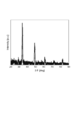
- FIG. 3 shows XRD measurement results. As shown in FIG. 3, peak shifts toward high angles were observed in all EuS nanocrystal-derived signals. The peak shift toward the high angle side is considered to reflect the structure due to Mn doping. Moreover, the average particle diameter calculated using the Scherrer equation from the result of XRD measurement was about 11.47 nm, which was different from the average particle diameter in the TEM image.
- FIG. 6 is a TEM image of EuS nanocrystals. As shown in FIG. 6, it was confirmed that the EuS crystal was nano-sized.
- FIG. 7 shows the particle size distribution of the TEM image of FIG. 6, where the horizontal axis is the particle size [nm] and the vertical axis is the number. As shown in FIG. 7, the average particle size was about 11.53 nm.
- 8 and 9 are the XRD measurement results of EuS nanocrystals and the XRD measurement results of MnS nanocrystals, respectively. As shown in FIGS. 8 and 9, both EuS and MnS had a NaCl structure.
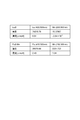
- FIG. 10 shows the measurement results of ICP emission analysis.
- the upper table in the figure is the measurement result of ICP emission analysis of EuS nanocrystals
- the lower table in the figure is the measurement result of ICP emission analysis of EuS: Mn nanocrystals.
- EuS nanocrystals do not contain Mn
- EuS: Mn nanocrystals have a Mn element concentration of 1.04 with respect to a Eu element concentration of 2.43 [ ⁇ mol / l]. [ ⁇ mol / l].
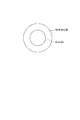
- EuS: Mn nanocrystals are in the form shown in FIG. That is, it is assumed that the EuS: Mn particle has a structure in which a film containing Mn covers the outside like a shell.
- the film containing Mn is assumed to be about 10.63 nm.
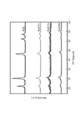
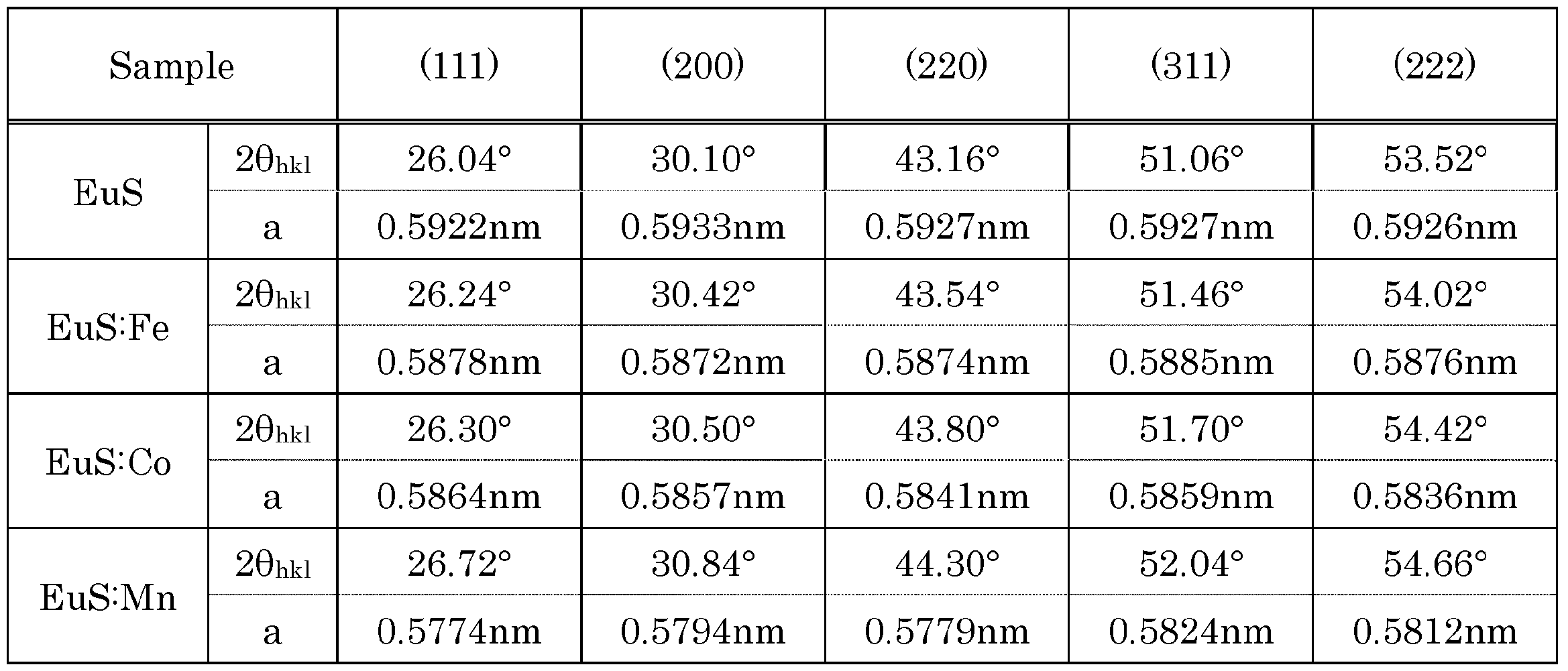
- FIG. 12 shows XRD measurement results of EuS: Fe nanocrystals and EuS: Co nanocrystals in addition to EuS nanocrystals and EuS: Mn nanocrystals.
- the lattice constant a can be obtained from the measurement result.
- 2 ⁇ hkl [°] and lattice constant a [nm] are as shown in Table 1 below.
- the upper stage in the frame shows the scattering angle 2 ⁇ hkl of (hkl)
- the lower part in the frame shows the lattice constant a calculated using the scattering angle 2 ⁇ hkl .
- the lattice constant a of EuS nanocrystals doped with Mn, Fe or Co was smaller than that of EuS nanocrystals alone.
- transition metals such as Mn, Fe, and Co
- Mn, Fe, and Co transition metals
- the doping of the transition metal acts to reduce the lattice constant a.
- the thin film according to the embodiment of the present invention is a thin film made of crystalline Eu (II) compound nanocrystals doped with metal ions.
- the film thickness is, for example, about 5 nm to 100 ⁇ m.
- the size of the Eu (II) compound nanoparticles doped with metal ions is, for example, an average particle diameter of about 5 nm to 100 nm.
- As a material for Eu (II) compound nanoparticles for example, EuO, EuS, EuSe, or EuTe europium chalcogenide is used. Transition metals are used. For example, Mn, Cr, Fe, Co, Ni, Cu, Ag, Zn, Cd, or a combination thereof is used. Further, the concentration of the metal ions may be in the range of about 0.1% to 49% by mass percentage.
- the metal ions doped in the nanocrystals affect the magneto-optical properties of the Eu (II) compound nanoparticles.
- the magneto-optical effect of the Eu (II) compound nanoparticles themselves can be increased.
- the Faraday effect in a wide range from the ultraviolet region to the infrared region can be exhibited at room temperature due to the quantum size effect. For this reason, it can be used as an optical element corresponding to a wide wavelength region.
- Eu (III) carbamide complex which is a raw material for synthesis of EuS nanocrystals: [Eu (PPh 4 ) (S 2 CNEt 2 )], and a complex for Mn doping: [Mn (S 2 CNEt 2 ) 3 )] Prepare.
- the Eu (III) carbamide complex, the complex for Mn doping, and the supporting electrolyte are dispersed in a solvent.
- a solvent for example, tetrabutylammonium (III) is used as the supporting electrolyte.
- acetonitrile is used as the solvent.
- a transparent electrode is used as the working electrode WE for thin-film electrochemical synthesis, and the transparent electrode WE, the reference electrode RE, and the counter electrode CE are inserted into a solvent and degassed with Ar. Apply.
- the transparent electrode for example, tin-doped indium oxide (ITO: Indium Tin Oxide) is used, and platinum (Pt) is used as the reference electrode and the counter electrode.
- ITO Indium Tin Oxide
- Pt platinum
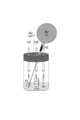
- FIG. 14 is a schematic configuration diagram of an optical isolator conventionally used. As shown in FIG. 14, the optical isolator has a structure in which a Faraday rotator 10 is placed between a polarizer 11 and an analyzer 12 and is sandwiched between permanent magnets 13 that apply a magnetic field to the Faraday rotator 10. .
- the forward light introduced from the optical fiber 14a is linearly polarized by the polarizer 11, and then the light whose polarization plane is rotated by the Faraday rotator 10 passes through the analyzer 12 to the optical fiber 14b. be introduced.
- the light in the reverse direction is linearly polarized by the analyzer 12 and its plane of polarization is rotated by the Faraday rotator 10, but the rotated light does not coincide with the plane of polarization of the polarizer 11. Cannot pass through the polarizer 11 and the return light is blocked there.
- a Faraday rotator 10 made of garnet crystal has been used.
- the Faraday rotator 10 is formed using the nanocrystal or thin film containing the Eu (II) compound described above, the same polarization plane rotation effect as that of the Faraday rotator 10 made of garnet crystal can be obtained. For this reason, it is possible to manufacture an optical isolator for home short-range communication at low cost.
- optical isolator currently on the market corresponds only to the near infrared region, but the optical isolator in which the Faraday rotator 10 is formed using the nanocrystal or thin film containing the Eu (II) compound described above is ultraviolet and It corresponds to the visible region, and can also be used when multiwavelength communication is to be performed in the near future.
- the composite nanocrystal and composite thin film containing the above-described Eu (II) compound can be applied to an optical switch using the magneto-optical effect.
- it can be employed as a Faraday rotation element of an optical switch.
- the thin film which has a new characteristic can be produced
- a solution containing the above-described composite nanocrystal is made into a colloidal solution by hydrolysis and condensation polymerization reaction, and further, the reaction is promoted to form a gel that loses fluidity.
- An inorganic glass thin film containing nanocrystals can be produced.
- a polymer thin film containing the composite nanocrystal can be generated by dispersing the above-described composite nanocrystal in a dissolved polymer and spraying it on a plate or the like to dry.
- a recording medium such as a magneto-optical disk capable of writing and reading data using the Kerr effect of the Eu (II) compound rotating the polarization direction of the reflected light
- a recording medium such as a magneto-optical disk capable of writing and reading data using the Kerr effect of the Eu (II) compound rotating the polarization direction of the reflected light
- It can be produced using nanocrystals containing.
- a laser beam is applied to a recording surface made of a resin thin film containing nanocrystals on the disk surface with a magnetic field not strong enough to reverse the magnetization direction applied in the direction opposite to the magnetization direction.
- the magnetization direction is reversed only in the portion irradiated with the laser beam, and data is written.
- a laser beam weaker than the writing light is applied to the recording surface, and the difference in the Kerr rotation angle of the reflected light is detected using the polar Kerr effect. That is, the recorded signal can be read by detecting the difference in Kerr rotation angle as a change in light intensity using a polarizer.
- the Faraday rotation coefficient can be arbitrarily increased in a wavelength band where the light transmission loss is small. For this reason, it is possible to provide an optical device that cannot be realized by conventional techniques, such as an optical isolator having two wavelengths formed by one optical isolator.
- Example 1 Mn-doped EuS nanocrystals were prepared by the manufacturing method shown in the embodiment.
- Example 2 Fe-doped EuS nanocrystals were prepared by the manufacturing method shown in the embodiment.
- Example 3 Co-doped EuS nanocrystals were prepared by the manufacturing method shown in the embodiment.
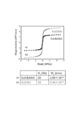
- Example 1 (Evaluation of magnetic properties) For Example 1 and Comparative Example 1, the MH loop was measured. The measurement results are shown in FIG. As shown in FIG. 15, the coercive force H C of Comparative Example 1 was 20 Oe, and the saturation magnetization M S was 2.89 ⁇ 10 ⁇ 21 emu. In contrast, the coercive force H C of the example was 24 Oe, and the saturation magnetization M S was 5.44 ⁇ 10 ⁇ 21 emu. Thus, large despite increased magnitude of the coercive force H C compared with Comparative Example 1 and Example 1 did not change. On the other hand, the saturation magnetization M S of Example 1, was about 1.88 times the saturation magnetization M S of Comparative Example 1. The increase in saturation magnetization is thought to be due to Eu 2+ -Mn 2+ interaction. Thus, since the improvement of the saturation magnetization was observed, it was shown that Mn doping into EuS is effective in improving the magnetic characteristics.
- Examples 1 to 3 and Comparative Example 2 were measured at a low temperature (1.8 K). As measurement samples, Examples 1 to 3 and Comparative Example 2 were used.
- FIG. 16 is a partially enlarged view of the MH loop. In FIG. 16, Example 1 is indicated by a solid line, and Comparative Example 2 is indicated by a dotted line.
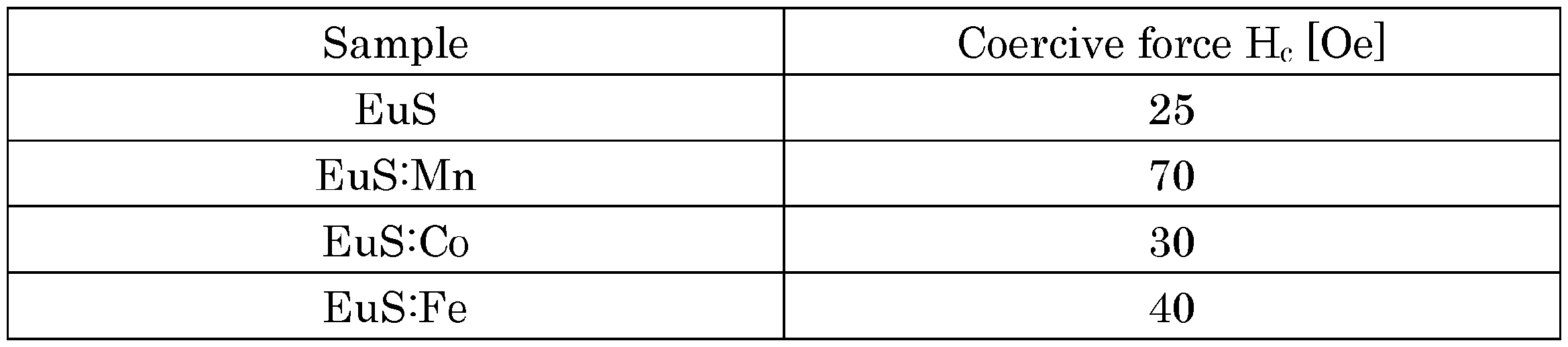
- the coercive force Hc of Example 1 was 70 Oe, which was larger than the coercive force Hc (25 Oe) of Comparative Example 2.
- the coercive force Hc was similarly evaluated for Examples 2 and 3. The results are shown in Table 2.
- the magnitude relationship of the coercive force Hc between the nanocrystals was Hc (EuS: Mn)> Hc (EuS: Fe)> Hc (EuS: Co)> Hc (EuS). It is presumed that the coercive force Hc is increased because the transition metal ions (Mn, Fe, Co) introduced into the crystal lattice hinder the rotation of the magnetic moment of Eu (II) ions. Thus, since the improvement of the coercive force was observed, it was shown that doping of transition metal ions (Mn, Fe, Co) into EuS is effective in improving the magnetic properties.
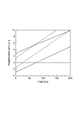
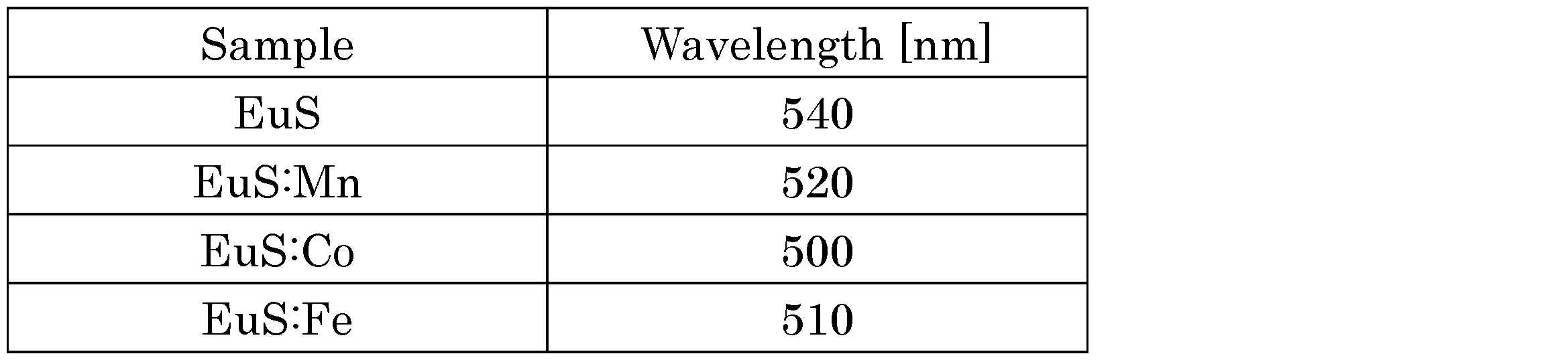
- Example 1 and Comparative Example 2 were dissolved in toluene, and light absorption in the wavelength range of ultraviolet-visible light was measured. The measurement results are shown in FIG. In FIG. 17, the horizontal axis represents wavelength and the vertical axis represents absorbance abs. As shown in FIG. 17, it was confirmed that Example 1 showed higher absorption characteristics than Comparative Example 2 at wavelengths of 350 nm to 650 nm. That is, it was confirmed that the absorption peak shifts to the short wavelength side by Mn doping. Next, Examples 1 to 3 and Comparative Example 2 were dissolved in toluene, and light absorption in the wavelength range of 300 nm to 800 nm was measured.
- the horizontal axis represents wavelength
- the vertical axis represents absorbance abs.
- the absorption peak shifts to the short wavelength side due to the transition metal ion (Mn, Fe, Co) doping. Details of the absorption peak are shown in Table 3 below. As shown in Table 3, it was confirmed that Examples 1 to 3 showed higher absorption characteristics than Comparative Example 2.
- Verde constant spectra were measured at room temperature.
- the Verde constant V can be calculated by the following formula (1) using the rotation angle (Faraday angle) ⁇ of linearly polarized light, the magnetic field H, and the thickness l of the sample.
- the thickness l of the sample has the relationship shown in the following equation (2) with the absorbance abs (Lambert Beer rule). Therefore, from Formula (1) and Formula (2), the Verde constant V normalized by the absorbance abs is expressed by the following Formula (3).
- the sample concentration c is also a standardized Verde constant. Therefore, the Verde constant can be evaluated without measuring the sample thickness l and the sample concentration c by first measuring the absorbance abs and normalizing the measured absorbance abs.
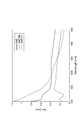
- Example 20 is the wavelength, and the vertical axis is the normalized Verde constant [degOe ⁇ 1 abs ⁇ 1 ].
- Table 5 shows the standardized Verde constant of each sample and the wavelength at that time. As shown in FIG. 20 and Table 5, it was confirmed that Examples 1 and 2 can obtain an enhancing effect on magneto-optical characteristics as compared with Comparative Example 2.
Landscapes
- Chemical & Material Sciences (AREA)
- Engineering & Computer Science (AREA)
- Physics & Mathematics (AREA)
- Nanotechnology (AREA)
- Organic Chemistry (AREA)
- General Physics & Mathematics (AREA)
- Nonlinear Science (AREA)
- Crystallography & Structural Chemistry (AREA)
- Inorganic Chemistry (AREA)
- Life Sciences & Earth Sciences (AREA)
- Optics & Photonics (AREA)
- Condensed Matter Physics & Semiconductors (AREA)
- Geology (AREA)
- Power Engineering (AREA)
- Composite Materials (AREA)
- Materials Engineering (AREA)
- Biophysics (AREA)
- Manufacturing & Machinery (AREA)
- Optical Modulation, Optical Deflection, Nonlinear Optics, Optical Demodulation, Optical Logic Elements (AREA)
- Compounds Of Alkaline-Earth Elements, Aluminum Or Rare-Earth Metals (AREA)
Abstract
Description
本発明の実施形態に係るナノ結晶は、金属イオンがドープされた結晶性のEu(II)化合物ナノ結晶である。金属イオンがドープされたEu(II)化合物ナノ粒子の大きさは、例えば平均粒径が約5nm~100nmである。Eu(II)化合物ナノ粒子の材料としては、例えば、EuO,EuS,EuSe又はEuTeのユーロピウムカルコゲナイドが用いられる。金属イオンの材料としては、遷移金属が用いられる。例えばMn、Cr、Fe、Co、Ni、Cu、Ag、ZnもしくはCd又はこれらの組み合わせが用いられる。また、金属イオンの濃度は、質量百分率で約0.1%~49%の範囲であればよい。さらに、金属イオンがドープされたEu(II)化合物ナノ粒子は、当該遷移金属により被覆されていてもよい。
実施形態に係るナノ結晶の製造方法について図1を用いて説明する。なお、以下では説明理解の容易性を考慮し、Eu(II)化合物としてEuS(硫化ユーロピウム)、金属としてMnを用いた場合を説明する。

本発明の実施形態に係る薄膜は、金属イオンがドープされた結晶性のEu(II)化合物ナノ結晶からなる薄膜である。膜厚は、例えば約5nm~100μmである。金属イオンがドープされたEu(II)化合物ナノ粒子の大きさは、例えば平均粒径が約5nm~100nmである。Eu(II)化合物ナノ粒子の材料としては、例えば、EuO,EuS,EuSe又はEuTeのユーロピウムカルコゲナイドが用いられる。遷移金属が用いられる。例えばMn、Cr、Fe、Co、Ni、Cu、Ag、ZnもしくはCd又はこれらの組み合わせが用いられる。また、金属イオンの濃度は、質量百分率で約0.1%~49%の範囲であればよい。
実施形態に係る薄膜の製造方法について説明する。なお、以下では説明理解の容易性を考慮し、Eu(II)化合物としてEuS(硫化ユーロピウム)、金属としてMnを用いた場合を説明する。
上述したEu(II)化合物を含む複合ナノ結晶及び複合薄膜は、大きなファラデー効果を奏するため、光磁気材料として応用することができる。例えば、戻り光を防止するために光通信などで用いられている光アイソレータなどへの適用が考えられる。図14は、従来から用いられている光アイソレータの概略構成図である。図14に示すように、光アイソレータは、ファラデー回転子10が偏光子11と検光子12の間に置かれ、ファラデー回転子10に磁場を印加する永久磁石13に挟まれた構造となっている。光アイソレータでは、光ファイバ14aから導入された順方向の光は偏光子11により直線偏光にされた後、ファラデー回転子10により偏光面が回転した光が検光子12を通過して光ファイバ14bに導入される。一方、逆方向の光(戻り光)は検光子12により直線偏光にされ、ファラデー回転子10によりその偏光面が回転するが、回転後の光は偏光子11とは偏光面が一致しないため光は偏光子11を通過できず、戻り光がそこで遮断されるようになっている。ファラデー回転子10として、従来はガーネット結晶製のもの等を用いていた。上述したEu(II)化合物を含むナノ結晶又は薄膜を用いてファラデー回転子10を形成した場合であっても、ガーネット結晶製のファラデー回転子10と同様の偏光面回転効果を得ることができる。このため、家庭用の短距離通信用光アイソレータを安価に作製することが可能である。
また、上述したEu(II)化合物を含む複合ナノ結晶を無機ガラス薄膜やポリマー薄膜に含有させることにより新たな特性を有する薄膜を生成することができる。例えば、上述した複合ナノ結晶を含有した溶液を、加水分解及び縮重合反応によりコロイド溶液とし、さらに反応を促進させることにより流動性を失ったゲルを形成し、このゲルを熱処理することにより、複合ナノ結晶を含有した無機ガラス薄膜を生成することができる。また、例えば、上述した複合ナノ結晶を溶解したポリマーに分散させて板等に吹き付けて乾かすことにより、複合ナノ結晶を含有したポリマー薄膜を生成することができる。
実施形態に示す製造方法でMnドープのEuSナノ結晶を作成した。
(実施例2)
実施形態に示す製造方法でFeドープのEuSナノ結晶を作成した。
(実施例3)
実施形態に示す製造方法でCoドープのEuSナノ結晶を作成した。
実施形態に示す製造方法でEuSナノ結晶及びMnSナノ結晶を作成し、これらの混合物を作成した。EuSとMnSとの混合比は、10:1とした。
(比較例2)
実施形態に示す製造方法でEuSナノ結晶を作成した。
実施例1及び比較例1について、MHループを測定した。測定結果を図15に示す。図15に示すように、比較例1の保磁力HCは20Oe、飽和磁化MSは2.89×10⁻²¹emuであった。これに対して、実施例の保磁力HCは24Oe、飽和磁化MSは5.44×10⁻²¹emuであった。このように、実施例1と比較例1とを比べると保磁力HCの大きさは増加したものの大きくは変化しなかった。一方、実施例1の飽和磁化MSは、比較例1の飽和磁化MSの約1.88倍となった。飽和磁化の増加は、Eu2+-Mn2+相互作用によるものと考えられる。このように、飽和磁化の向上が観測されたことから、EuS中へのMnドープは磁気特性向上に効果的であることが示された。
実施例1~3及び比較例2について光吸収を測定した。最初に、実施例1及び比較例2について、トルエンに溶解させて、紫外可視光の波長範囲での光吸収を測定した。測定結果を図17に示す。図17の横軸は波長、縦軸は吸収度absである。図17に示すように、波長350nm~650nmにおいて、実施例1は、比較例2に比べて高い吸収特性を示すことが確認された。すなわち、Mnドープによって吸収ピークが短波長側にシフトすることが確認された。次に、実施例1~3及び比較例2について、トルエンに溶解させて、波長300nm~800nmの範囲での光吸収を測定した。測定結果を図18に示す。図18の横軸は波長、縦軸は吸収度absである。図18に示すように、遷移金属イオン(Mn,Fe,Co)ドープによって吸収ピークが短波長側にシフトすることが確認された。吸収ピークの詳細を以下の表3に示す。
実施例1,2及び比較例2について、室温においてベルデ定数スペクトルを測定した。通常、ベルデ定数Vは、直線偏光の回転角(ファラデー角)α、磁場H、サンプルの厚さlを用いて、以下の数式(1)で算出することができる。





Claims (10)
- 遷移金属のイオンがドープされたEu(II)化合物のナノ結晶。
- 前記Eu(II)化合物のナノ粒子は、EuO,EuS,EuSe又はEuTeから選択される材料により形成される請求項1記載のナノ結晶。
- 前記イオンはMn,Fe又はCoのイオンであり、
Mn,Fe又はCoを含有する膜で被覆された請求項1又は2に記載のナノ結晶。 - 遷移金属のイオンがドープされたEu(II)化合物の薄膜。
- 請求項1~3の何れか一項に記載のナノ結晶又は請求項4の記載の薄膜を用いて形成された光磁気材料。
- 請求項1~3の何れか一項に記載のナノ結晶を含む無機ガラス薄膜。
- 請求項1~3の何れか一項に記載のナノ結晶を含むポリマー薄膜。
- 請求項1~3の何れか一項に記載のナノ結晶、請求項4の記載の薄膜、請求項5に記載の光磁気材料、請求項6に記載の無機ガラス薄膜又は請求項7に記載のポリマー薄膜を用いて形成されたファラデー回転子を備える光アイソレータ。
- Eu(III)を含有する錯体及び遷移金属を含有する錯体を溶媒に分散させるステップと、
前記溶媒を熱還元反応させることによって前記遷移金属のイオンがドープされたEu(II)化合物のナノ結晶を合成するステップと、
を備えるナノ結晶の製造方法。 - 電気化学的に薄膜を製造する製造方法であって、
Eu(III)を含有する錯体及び遷移金属を含有する錯体を溶媒に分散させるステップと、
透明電極を作用電極とし、前記溶媒中に前記透明電極を挿入して電圧を印加することにより前記透明電極に前記遷移金属のイオンがドープされたEu(II)化合物からなる薄膜を形成するステップと、
を備えることを特徴とする薄膜の製造方法。
Priority Applications (2)
| Application Number | Priority Date | Filing Date | Title |
|---|---|---|---|
| US14/002,895 US9280002B2 (en) | 2011-03-04 | 2012-03-01 | Thin film and nanocrystals of europium(II) compound doped with metal ions |
| JP2013503486A JP5896361B2 (ja) | 2011-03-04 | 2012-03-01 | 金属イオンドープEu(II)化合物のナノ結晶及び薄膜 |
Applications Claiming Priority (2)
| Application Number | Priority Date | Filing Date | Title |
|---|---|---|---|
| JP2011-047623 | 2011-03-04 | ||
| JP2011047623 | 2011-03-04 |
Publications (1)
| Publication Number | Publication Date |
|---|---|
| WO2012121112A1 true WO2012121112A1 (ja) | 2012-09-13 |
Family
ID=46798078
Family Applications (1)
| Application Number | Title | Priority Date | Filing Date |
|---|---|---|---|
| PCT/JP2012/055264 Ceased WO2012121112A1 (ja) | 2011-03-04 | 2012-03-01 | 金属イオンドープEu(II)化合物のナノ結晶及び薄膜 |
Country Status (3)
| Country | Link |
|---|---|
| US (1) | US9280002B2 (ja) |
| JP (1) | JP5896361B2 (ja) |
| WO (1) | WO2012121112A1 (ja) |
Citations (3)
| Publication number | Priority date | Publication date | Assignee | Title |
|---|---|---|---|---|
| JP2001354417A (ja) * | 2000-06-12 | 2001-12-25 | Japan Science & Technology Corp | ナノサイズの希土類酸化物又は硫化物及びそれらの光化学反応を用いた製法。 |
| JP2004354927A (ja) * | 2003-05-30 | 2004-12-16 | Kansai Tlo Kk | ナノサイズのEuO結晶又はEuS結晶を含有する光磁気応答性プラスチック |
| WO2007102271A1 (ja) * | 2006-03-09 | 2007-09-13 | National University Corporation NARA Institute of Science and Technology | ナノサイズEuSe結晶及びナノサイズEuSe結晶の製造方法 |
Family Cites Families (2)
| Publication number | Priority date | Publication date | Assignee | Title |
|---|---|---|---|---|
| US7993541B1 (en) * | 2002-05-10 | 2011-08-09 | Nanocrystals Technology Lp | Quantum confined atom (QCA) based nanomagnets |
| JP5392694B2 (ja) | 2007-03-28 | 2014-01-22 | 国立大学法人豊橋技術科学大学 | 磁気光学体 |
-
2012
- 2012-03-01 WO PCT/JP2012/055264 patent/WO2012121112A1/ja not_active Ceased
- 2012-03-01 US US14/002,895 patent/US9280002B2/en not_active Expired - Fee Related
- 2012-03-01 JP JP2013503486A patent/JP5896361B2/ja not_active Expired - Fee Related
Patent Citations (3)
| Publication number | Priority date | Publication date | Assignee | Title |
|---|---|---|---|---|
| JP2001354417A (ja) * | 2000-06-12 | 2001-12-25 | Japan Science & Technology Corp | ナノサイズの希土類酸化物又は硫化物及びそれらの光化学反応を用いた製法。 |
| JP2004354927A (ja) * | 2003-05-30 | 2004-12-16 | Kansai Tlo Kk | ナノサイズのEuO結晶又はEuS結晶を含有する光磁気応答性プラスチック |
| WO2007102271A1 (ja) * | 2006-03-09 | 2007-09-13 | National University Corporation NARA Institute of Science and Technology | ナノサイズEuSe結晶及びナノサイズEuSe結晶の製造方法 |
Non-Patent Citations (4)
| Title |
|---|
| HIROKI NAKAO ET AL.: "EuS-Au Fukugo Nano Ryushi no Gosei Oyobi Hikari Jiki Tokusei no Hyoka", KOEN YOKOSHU, vol. 90, no. 3, 2010, pages 921 * |
| MASASHI MAEDA ET AL.: "Hikari Jiki Tokusei o Yusuru EuS Nano Kessho eno Sen'i Kinzoku Dope", 2011 NEN SYMPOSIUM ON PHOTOCHEMISTRY, 1 September 2011 (2011-09-01), pages 51 * |
| SROTOSWINI KAR ET AL.: "Gadolinium Doped Europium Sulfide", J. AM. CHEM. SOC., vol. 132, no. 40, 2010, pages 13960 - 13962 * |
| T.R MCGUIRE ET AL.: "Magnetic and magneto- optical properties of Fe-doped EuO films", JOURNAL OF APPLIED PHYSICS, vol. 42, no. 4, 1971, pages 1775 - 1777 * |
Also Published As
| Publication number | Publication date |
|---|---|
| JP5896361B2 (ja) | 2016-03-30 |
| US9280002B2 (en) | 2016-03-08 |
| US20140071527A1 (en) | 2014-03-13 |
| JPWO2012121112A1 (ja) | 2014-07-17 |
Similar Documents
| Publication | Publication Date | Title |
|---|---|---|
| Iranizad et al. | Nonlinear optical properties of nematic liquid crystal doped with different compositional percentage of synthesis of Fe3O4 nanoparticles | |
| Drofenik et al. | Hydrothermal synthesis of Ba‐hexaferrite nanoparticles | |
| Moussa et al. | Chromium doped ZnO nanoparticles for energy storage, gas and humidity sensing and spin based electronic devices applications | |
| Regulacio et al. | Magnetic properties of lanthanide chalcogenide semiconducting nanoparticles | |
| Kim et al. | Dynamic magnetic field alignment and polarized emission of semiconductor nanoplatelets in a liquid crystal polymer | |
| Zhang et al. | XMCD and XMCD‐PEEM Studies on Magnetic‐Field‐Assisted Self‐Assembled 1D Nanochains of Spherical Ferrite Particles | |
| Chen et al. | Mixed valence effects in TbVO4: Y nanocrystals and diamagnetic materials: Structure, optical linear & nonlinear, magnetic and Faraday rotation properties | |
| Chen et al. | High polarizability enhanced EPR, optical linear & nonlinear and electric conductivity: Role of NiFe2O4 nanocrystals in transparent tellurite glass-ceramics | |
| Pazhanivelu et al. | Influence of Co ions doping in structural, vibrational, optical and magnetic properties of ZnO nanoparticles | |
| Mansour et al. | Structure, morphology, optical and magnetic studies of Fe3O4-doped CdS nanocomposite | |
| Kumar et al. | Tuning of structural, elastic, luminescence, magnetic, and multiferroic properties of rare earth Ce3+ substituted strontium hexaferrite Ceramic magnetic nanomaterials for its industrial applications | |
| Chen et al. | Giant Faraday rotation, magnetic and nonlinearity of diamagnetic glass tailored by plasmonic-magnetic bimetallic Au-Ni NPs | |
| Hasegawa et al. | First synthesis of EuS nanoparticle thin film with a wide energy gap and giant magneto-optical efficiency on a glass electrode | |
| Binish et al. | Defect state enhanced nonlinear absorption and optical limiting behaviour of erbium doped silver molybdate nanostructures | |
| Poornaprakash et al. | CdS: Eu quantum dots for spintronics and photocatalytic applications | |
| Chen et al. | Structure, EPR, and Mössbauer spectra of La0. 8Sr0. 2FeO3 nanocrystals modified magnetic glass-ceramics | |
| Egashira et al. | Effects of some transition metal ions on the visible and infrared Faraday rotation of gadolinium iron garnet | |
| JP5896361B2 (ja) | 金属イオンドープEu(II)化合物のナノ結晶及び薄膜 | |
| Bayappagari et al. | Structural, optical and magnetic properties of vacuum annealed Fe, Mn doped NiO nanoparticles | |
| Sharma et al. | Exchange-coupling enhanced: Tailoring structural and magnetic properties of Dy iron garnet ferrite nanoparticles via La substitution for switching devices | |
| JP6021113B2 (ja) | Eu(II)化合物及び金属を含有するナノ結晶及び薄膜 | |
| Kathiravan et al. | Mn doping nanoarchitectonics of NiO nanoparticles with various property impacts for optoelectronic devices and diluted magnetic semiconductor applications | |
| Panmand et al. | Growth of Bi 2 Te 3 quantum dots/rods in glass: a unique highly stable nanosystem with novel functionality for high performance magneto optical devices | |
| Pascu et al. | Magneto-optical characterization of colloidal dispersions. application to nickel nanoparticles | |
| Wang et al. | Polar Solvent‐Assisted Chiral Ligand and Cation Exchange for Bright, Strongly Circularly Polarized Emission in CsPbBr3 Perovskite Nanoplatelets |
Legal Events
| Date | Code | Title | Description |
|---|---|---|---|
| 121 | Ep: the epo has been informed by wipo that ep was designated in this application |
Ref document number: 12754376 Country of ref document: EP Kind code of ref document: A1 |
|
| DPE1 | Request for preliminary examination filed after expiration of 19th month from priority date (pct application filed from 20040101) | ||
| ENP | Entry into the national phase |
Ref document number: 2013503486 Country of ref document: JP Kind code of ref document: A |
|
| NENP | Non-entry into the national phase |
Ref country code: DE |
|
| WWE | Wipo information: entry into national phase |
Ref document number: 14002895 Country of ref document: US |
|
| 122 | Ep: pct application non-entry in european phase |
Ref document number: 12754376 Country of ref document: EP Kind code of ref document: A1 |