WO2012114501A1 - 脳プローブ及びその製造方法 - Google Patents
脳プローブ及びその製造方法 Download PDFInfo
- Publication number
- WO2012114501A1 WO2012114501A1 PCT/JP2011/054246 JP2011054246W WO2012114501A1 WO 2012114501 A1 WO2012114501 A1 WO 2012114501A1 JP 2011054246 W JP2011054246 W JP 2011054246W WO 2012114501 A1 WO2012114501 A1 WO 2012114501A1
- Authority
- WO
- WIPO (PCT)
- Prior art keywords
- electrode
- probe
- electrode plate
- brain
- arrangement pattern
- Prior art date
Links
Images


Classifications
-
- H—ELECTRICITY
- H01—ELECTRIC ELEMENTS
- H01R—ELECTRICALLY-CONDUCTIVE CONNECTIONS; STRUCTURAL ASSOCIATIONS OF A PLURALITY OF MUTUALLY-INSULATED ELECTRICAL CONNECTING ELEMENTS; COUPLING DEVICES; CURRENT COLLECTORS
- H01R11/00—Individual connecting elements providing two or more spaced connecting locations for conductive members which are, or may be, thereby interconnected, e.g. end pieces for wires or cables supported by the wire or cable and having means for facilitating electrical connection to some other wire, terminal, or conductive member, blocks of binding posts
- H01R11/11—End pieces or tapping pieces for wires, supported by the wire and for facilitating electrical connection to some other wire, terminal or conductive member
- H01R11/18—End pieces terminating in a probe
-
- A—HUMAN NECESSITIES
- A61—MEDICAL OR VETERINARY SCIENCE; HYGIENE
- A61B—DIAGNOSIS; SURGERY; IDENTIFICATION
- A61B5/00—Measuring for diagnostic purposes; Identification of persons
- A61B5/24—Detecting, measuring or recording bioelectric or biomagnetic signals of the body or parts thereof
-
- A—HUMAN NECESSITIES
- A61—MEDICAL OR VETERINARY SCIENCE; HYGIENE
- A61B—DIAGNOSIS; SURGERY; IDENTIFICATION
- A61B5/00—Measuring for diagnostic purposes; Identification of persons
- A61B5/24—Detecting, measuring or recording bioelectric or biomagnetic signals of the body or parts thereof
- A61B5/25—Bioelectric electrodes therefor
- A61B5/279—Bioelectric electrodes therefor specially adapted for particular uses
- A61B5/291—Bioelectric electrodes therefor specially adapted for particular uses for electroencephalography [EEG]
- A61B5/293—Invasive
-
- A—HUMAN NECESSITIES
- A61—MEDICAL OR VETERINARY SCIENCE; HYGIENE
- A61N—ELECTROTHERAPY; MAGNETOTHERAPY; RADIATION THERAPY; ULTRASOUND THERAPY
- A61N1/00—Electrotherapy; Circuits therefor
- A61N1/02—Details
- A61N1/04—Electrodes
- A61N1/05—Electrodes for implantation or insertion into the body, e.g. heart electrode
- A61N1/0526—Head electrodes
- A61N1/0529—Electrodes for brain stimulation
- A61N1/0534—Electrodes for deep brain stimulation
-
- A—HUMAN NECESSITIES
- A61—MEDICAL OR VETERINARY SCIENCE; HYGIENE
- A61B—DIAGNOSIS; SURGERY; IDENTIFICATION
- A61B2562/00—Details of sensors; Constructional details of sensor housings or probes; Accessories for sensors
- A61B2562/04—Arrangements of multiple sensors of the same type
- A61B2562/046—Arrangements of multiple sensors of the same type in a matrix array
-
- A—HUMAN NECESSITIES
- A61—MEDICAL OR VETERINARY SCIENCE; HYGIENE
- A61B—DIAGNOSIS; SURGERY; IDENTIFICATION
- A61B2562/00—Details of sensors; Constructional details of sensor housings or probes; Accessories for sensors
- A61B2562/12—Manufacturing methods specially adapted for producing sensors for in-vivo measurements
- A61B2562/125—Manufacturing methods specially adapted for producing sensors for in-vivo measurements characterised by the manufacture of electrodes
-
- H—ELECTRICITY
- H01—ELECTRIC ELEMENTS
- H01R—ELECTRICALLY-CONDUCTIVE CONNECTIONS; STRUCTURAL ASSOCIATIONS OF A PLURALITY OF MUTUALLY-INSULATED ELECTRICAL CONNECTING ELEMENTS; COUPLING DEVICES; CURRENT COLLECTORS
- H01R2201/00—Connectors or connections adapted for particular applications
- H01R2201/12—Connectors or connections adapted for particular applications for medicine and surgery
-
- Y—GENERAL TAGGING OF NEW TECHNOLOGICAL DEVELOPMENTS; GENERAL TAGGING OF CROSS-SECTIONAL TECHNOLOGIES SPANNING OVER SEVERAL SECTIONS OF THE IPC; TECHNICAL SUBJECTS COVERED BY FORMER USPC CROSS-REFERENCE ART COLLECTIONS [XRACs] AND DIGESTS
- Y10—TECHNICAL SUBJECTS COVERED BY FORMER USPC
- Y10T—TECHNICAL SUBJECTS COVERED BY FORMER US CLASSIFICATION
- Y10T29/00—Metal working
- Y10T29/49—Method of mechanical manufacture
- Y10T29/49002—Electrical device making
- Y10T29/49117—Conductor or circuit manufacturing
Definitions
- the present invention relates to a brain probe that detects an electrical signal from a brain cell and outputs an electrical signal that gives a stimulus to the brain cell, and a manufacturing method thereof.
- brain disorders for example, Parkinson's disease, motor paralysis, epilepsy, etc.
- diseases caused by brain disorders for example, Parkinson's disease, motor paralysis, epilepsy, etc.
- brain probes that are inserted into the brain and detect electrical signals (electroencephalograms) of brain cells have been used conventionally.
- brain probes are also used as means for applying electrical stimulation to the brain in order to identify the brain region where the disorder occurs.
- BMI Brain-Machine Interface
- BCI Brain-Computer Interface
- BMI is a system that directly connects the brain and machine to interact with each other, and is broadly divided into motor BMI, sensory BMI, and direct operation BMI.
- Motor BMI is a technology that controls external devices such as robots by detecting and using the activity that expresses motor output among the neural activities of the brain. For example, it is used to reconstruct motor function in patients with limb paralysis.
- Sensory BMI is a technology that generates and enhances various sensations by sending signals into the brain. Some sensory BMIs have already been put into practical use, and typical examples are cochlear implants and retinas.
- Directly operated BMI is a technology that restores various functions with disabilities by stimulating the brain directly.
- BCI is a general term for interfaces that allow computers to be operated simply by thinking by directly linking electrical signals that flow in the human brain to the computer.
- BCI there are two methods: reading a brain wave signal on the surface of the head using a hat-shaped electrode, and reading a neuron activity as a signal by embedding the electrode directly in the brain.
- DBS Deep Brain Stimulation
- a brain probe inserted into the brain to detect electrical signals in the brain and to apply electrical stimulation to the brain is, for example, manufactured by LSI (Large Scale Integration) as disclosed in Non-Patent Document 1 below.
- LSI Large Scale Integration
- an electrode is placed at the tip of a thin probe made of silicon of about several hundred microns, and the electrode is connected to a bonding pad on the other end side for connection to an external device via a lead wire.
- the brain probe proposed in Non-Patent Document 1 has a length (about 40 mm) that reaches the basal ganglia in the deep part of the cerebrum, and has an electrode on both sides as well as on one side of the tip. Yes. By arranging the electrodes on both sides, it becomes possible to detect electrical signals from both sides of the brain probe.
- the brain probe of Non-Patent Document 1 has the following problems. That is, the brain probe of Non-Patent Document 1 is fragile because it is entirely formed of a silicon substrate, and cannot be inserted alone when it is inserted deeply into the deep brain such as the basal ganglia. After inserting the metal tube into the brain using the metal tube as an auxiliary, the brain probe of Non-Patent Document 1 is inserted into the metal tube, thereby introducing the brain probe of Non-Patent Document 1 into the brain.
- Non-Patent Document 1 since the brain probe of Non-Patent Document 1 is arranged facing the front direction (normal direction) of each surface (front surface, back surface), the electrical signal from the front direction is compared with the electrical signal from the horizontal direction. Receiving with higher sensitivity, it is not possible to obtain sufficient reception sensitivity over the entire circumference of the brain probe. That is, there is a problem that even if electrodes are arranged on both sides, an electric signal from a specific direction cannot be received with sufficient sensitivity.
- an object of the present invention is to provide an omnidirectional brain probe that can be inserted independently up to the deep part of the brain and that can detect an electrical signal with higher sensitivity over the entire region, and a method for manufacturing the same.
- the configuration of the brain probe of the present invention that achieves the above object is a metal core probe and attached so as to cover the entire circumference of the side surface of the core probe, and the cross section is an n-gon (n is an integer of 3 or more). and n electrode plates forming n side surfaces, each electrode plate being provided with at least one electrode and a lead wiring extending from each electrode in the longitudinal direction of the side surface.
- a metal core probe By using a metal core probe, it has sufficient strength to be inserted deep into the brain, and by providing three or more electrode plates on the side surface, good sensitivity can be obtained over the entire 360 ° range with a single insertion. The result is an omnidirectional brain probe.
- the core probe has a tapered portion that narrows toward the tip and a same-diameter portion that extends from the tapered portion toward the other end, and the diameter of the same-diameter portion is smaller than the maximum diameter of the tapered portion.
- the diameter of the same diameter portion where the electrode plate is coated on the side surface of the core probe is substantially the same as or smaller than the maximum diameter of the tapered portion.
- the electrode plate is configured to have a silicon substrate.
- an electrode plate can be manufactured by an LSI manufacturing process.
- the electrode plate has six sides.
- the six surfaces have the advantage that two sets of three electrode plate arrangements for realizing omnidirectionality can be prepared, and the anisotropic etching of silicon single crystal can be used in the production of the electrode plates.
- Each of the three or more n electrode plates is arranged in, for example, a first electrode plate having a plurality of electrodes arranged in the first arrangement pattern, and a second arrangement pattern different from the first arrangement pattern.
- a second electrode plate having a plurality of electrodes.
- each of the n electrode plates includes, for example, a first electrode plate having a plurality of electrodes arranged in a first arrangement pattern and a plurality of electrodes arranged in a second arrangement pattern different from the first arrangement pattern. And a third electrode plate having a plurality of electrodes arranged in a third arrangement pattern different from the first arrangement pattern and the second arrangement pattern.
- n 6
- the first electrode plate, the second electrode plate, and the third electrode plate are attached so as to form two opposing side surfaces.
- the brain probe may further include a signal processing circuit that performs predetermined signal processing on a signal from the electrode and a signal output to the electrode, and is connected to a lead wiring extending from the electrode.
- the electrode plate includes a silicon substrate, and the signal processing circuit is formed on the silicon substrate. Thereby, the signal processing circuit and the brain probe can be integrated.
- the method of manufacturing a brain probe according to the present invention includes a step of manufacturing n (n is an integer of 3 or more) electrode plates each having at least one electrode and a lead wire extending from each electrode, and a cross section having an n-square shape (n And a step of attaching n electrode plates to the entire circumference of the side surface of the metal core probe so as to form n side surfaces that are an integer of 3 or more.
- a metal core probe By using a metal core probe, it has sufficient strength to be inserted deep into the brain, and by providing three or more electrode plates on the side surface, good sensitivity can be obtained over the entire 360 ° range with a single insertion. As a result, an omnidirectional brain probe can be manufactured.
- the n electrode plates are manufactured with their long sides connected, and attached so as to be wound around the side surface of the core probe. This makes it easy to attach a plurality of electrode plates.
- the n electrode plates are manufactured by connecting the long sides using a silicon substrate, and a groove is formed at the boundary between adjacent electrode plates by anisotropic etching.
- anisotropic etching property of silicon single crystal grooves can be easily formed at the boundary of connected electrode plates.
- the n electrode plates are manufactured using a silicon substrate, and a signal processing circuit that performs predetermined signal processing on a signal from the electrode and a signal output to the electrode and is connected to a lead wiring extending from the electrode, It is formed on the silicon substrate of each electrode plate.
- the signal processing circuit can be manufactured at the same time, and the signal processing circuit and the brain probe can be integrated.
- an omnidirectional brain probe that can be inserted independently up to the deep part of the brain and can detect and output an electrical signal with higher sensitivity over the entire circumference without variation in sensitivity depending on directions.
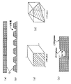
- FIG. 2 is a diagram illustrating an example of the shape of a core probe 10.
- FIG. It is a figure which shows the example of a shape of the electrode plate 12.
- FIG. 4 is a diagram for explaining a process of attaching an electrode plate 12 to the side surface of the core probe 10. It is an expanded sectional view of the same diameter part 10b where the electrode plate 12 was affixed.
- FIG. 5 is a view for explaining the structure of an electrode plate 12.
- 3 is a diagram illustrating an arrangement example of electrodes 14. It is a figure which shows another structural example of the brain probe in embodiment of this invention. It is a figure which shows the structural example of the brain probe which has four side surfaces.
- FIG. 1 It is a figure which shows the structural example of the brain probe which has a 3 side surface. It is a figure explaining the manufacturing process flow of the electrode plate. It is a figure explaining the manufacturing process flow of the electrode plate 12 (with a shield metal). It is a figure explaining the manufacturing process of the six electrode plates 12 with which the long side part was connected. It is a figure explaining arrangement
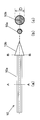
- FIG. 1 is a diagram showing a configuration example of a brain probe according to an embodiment of the present invention.
- 1A is an overview of the brain probe
- FIG. 1B is a cross-sectional view taken along the line AA in FIG. 1A
- FIG. 1C is a cross-sectional view taken along the line BB in FIG. is there.
- the brain probe 1 includes a core probe 10 and a plurality of electrode plates 12 that are attached to the side surface of the core probe 10 so as to cover the side surface of the core probe 10 and form six side surfaces.
- The By adopting a 6-sided electrode plate, an omnidirection brain probe that eliminates variations in receiving sensitivity depending on the direction and obtains good receiving sensitivity over the entire circumference compared to the 2-sided configuration is realized.
- the An omnidirectional brain probe can examine the neural activity in a fine area and adjust the stimulation position for the fine area. In order to achieve omnidirectionality, an electrode plate having three or more surfaces is required, but a six-surface electrode plate is the most preferable aspect in view of the manufacturing process and the possibility of use described later.
- the core probe 10 is made of a metal such as tungsten or platinum tungsten having sufficient hardness to be inserted into the deep part of the brain, and may be another metal or alloy that is hard and easy to process.
- the electrode plate 12 has at least one electrode on each side surface and a lead wiring extending from each electrode in the longitudinal direction of the side surface.
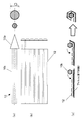
- FIG. 2 shows an example of the shape of the core probe 10 and FIG. 3 shows an example of the shape of the electrode plate 12.
- 2A is a schematic view of the core probe 10
- FIG. 2B is a cross-sectional view taken along the line AA in FIG. 2A
- FIG. 2C is a cross-sectional view taken along the line BB in FIG. It is.
- FIG. 3A shows a plane of the six electrode plates 12, and
- FIG. 3B shows a cross section of the six electrode plates.
- the core probe 10 has a tapered portion 10a that narrows toward the tip, and a same-diameter portion 10b that extends from the tapered portion toward the other end.
- the total length of the core probe 10 is about 40 mm
- the maximum diameter D of the tapered portion 10 a is about 200 ⁇ m
- the same diameter portion 10 b is about 140 ⁇ m.
- the side surface corresponding to the same diameter portion 10b is polished to form the same diameter portion 10b.
- the size is preferably as small as possible in consideration of the length to reach the basal ganglia of the cerebrum and invasiveness.
- the core is made of a metal probe, and a silicon substrate electrode plate is attached around the core, thereby ensuring the strength with which the brain probe can be inserted to the depth of the basal ganglia.
- the tapered portion 10a has a conical shape and has a circular cross section.
- the six side surfaces are provided in the same diameter portion 10b. That is, the cross section of the same-diameter portion 10b is hexagonal as shown in FIG. 2 (a), and the electrode plate 12 has a strip-like elongated shape, and the same-diameter portion 10b to which the electrode plate 12 is attached.
- the cross section of the electrode plate 12 is formed in a trapezoidal shape as shown in FIG. 3B so that the cross section also has a hexagonal shape.
- the six electrode plates 12 are attached to the respective side surfaces with an adhesive.
- the same-diameter portion 10b is preferably formed with six surfaces in accordance with the shape of the electrode plate 12, but is not limited thereto, and may be, for example, a circular cross section.
- the gap when the electrode plate 12 is attached can be filled with an adhesive.
- FIG. 4 is a diagram for explaining the process of attaching the electrode plate 12 to the side surface of the core probe 10.
- FIG. 4B six electrode plates 12 having long side portions connected to each other are formed, and as shown in FIG. 4C, the same-diameter portion 10b (FIG. 4A) of the core probe 10 is formed. Can be attached to the side of Of course, six electrode plates 12 may be generated one by one and attached individually to the side surface of the same diameter portion 10b of the core probe 10 one by one.
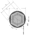
- FIG. 5 is an enlarged cross-sectional view of the same-diameter portion 10b to which the electrode plate 12 is attached.
- the cross section of the same diameter portion 10b is a regular hexagonal shape, and the diameter d1 is formed to be equal to or smaller than the maximum diameter D of the tapered portion 10a having a circular cross section, and the electrode plate 12 is attached to the side surface by the adhesive 13.
- the diameter d2 of the same diameter portion 10b to which the electrode plate 12 is attached does not exceed the maximum diameter D of the tapered portion 10a (preferably, the same diameter portion as the maximum diameter D).
- the thickness t1 of the electrode plate 12 and the thickness t2 of the adhesive 13 with respect to the diameter d1 are determined.
- FIG. 6 is a diagram for explaining the structure of the electrode plate 12.
- FIG. 6A is an electrode having four electrodes 14 and four bonding pads 18 connected to the electrodes 14 by lead wires 16.
- FIG. 6B is a plan view of the plate 12, and
- FIG. 6B is a cross-sectional view showing a wiring structure of electrodes and bonding pads. The wiring shown in FIG. 6A does not actually appear on the surface, but is shown for easy understanding of the explanation.
- the electrode plate 12 has an interlayer insulating film 12b on a silicon substrate 12a, and the electrode 14, the wiring 16, and the bonding pad 18 are formed on the interlayer insulating film 12b.
- the electrode plate 12 can be manufactured using an LSI manufacturing process, and the manufacturing process of the electrode plate 12 will be described later.
- the insulating substrate constituting the electrode plate 12 is not limited to the silicon substrate 12a and the interlayer insulating film 12b, and various insulating substrates using known insulating materials (alumina, ceramic, etc.) can be used. Any structure may be used as long as it has electrodes, wiring, and external connection terminals (bonding pads).
- a manufacturing process of LSI is used for manufacturing the electrode plate 12, a silicon substrate is used.
- An LSI that performs signal processing such as amplification and A / D conversion can be connected via a connector that is electrically connected to the bonding pad. That is, by mounting a very compact chip-like LSI at the base of the brain probe, a digital signal with less noise can be extracted from the brain probe itself without using an external large signal processing device.
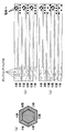
- FIG. 7 is a diagram illustrating an arrangement example of the electrodes 14. As shown in FIG. 7A, when the six electrode plates 12 are A to F planes, three arrangement patterns of the electrodes 14 are shown in FIGS. 7B and 7C.
- FIG. 7B shows an example in which electrodes are alternately arranged in two kinds of arrangement patterns every other surface.
- the A, C, and E planes are the first arrangement pattern in which the four electrodes 14 are arranged in a rhombus shape
- the B, D, and F planes are the first arrangement patterns in which the four electrodes 14 are arranged in series. This is a second arrangement pattern.
- simultaneous measurement with two types of arrangement patterns is possible, and each of the two types of arrangement patterns is arranged on three surfaces. Is possible.
- FIG. 7C shows an example in which the electrodes are arranged in three types of arrangement patterns in which the opposing surfaces have the same arrangement pattern.
- the A and D planes are the first arrangement pattern in which the four electrodes 14 are arranged in a diamond shape
- the B and E planes are the second arrangement pattern in which the four electrodes 14 are arranged in series.
- C and F planes are a third arrangement pattern in which the four electrodes 14 are arranged in a parallelogram shape.
- simultaneous measurement with three types of arrangement patterns is possible.
- all of the A to E planes may be the same arrangement pattern, or all may be different arrangement patterns. If all six surfaces have the same layout pattern, three surfaces are sufficient to ensure omnidirectionality. Therefore, in normal use, every other electrode plate is used, and the rest is reserved. Is possible.
- the number of electrodes per surface is not limited to the four illustrated, and the number is not limited. Furthermore, the number of electrodes may differ depending on the surface. Further, the arrangement pattern is not limited to that shown in the figure, and other patterns can be adopted according to the measurement / stimulation site, and the combination thereof can be determined as appropriate.
- Electrodes as many electrodes as possible and lead wires connected to them are formed on one electrode plate, and the electrode to be used is selected and electrically connected, so that one electrode plate can be electrically connected. , Can be used in various arrangement patterns.
- FIG. 8 is a diagram showing another configuration example of the brain probe according to the embodiment of the present invention.
- the configuration of FIG. 8A is a configuration in which a part of the side surface of the same diameter portion 10b of the core probe 10 is six as compared with the configuration of FIG.
- the tapered portion 10a has a conical shape as in the configuration of FIG.
- the tapered portion 10a has a hexagonal pyramid shape as compared with FIG.
- FIG. 9 shows a configuration example of a brain probe having four side surfaces
- FIG. 10 shows a configuration example of a brain probe having three side surfaces.
- the brain probe of the present invention is not limited to the six side surfaces described above, and may employ a configuration having three or more side surfaces.
- the cross section of the same-diameter portion 10b is a square, and the four electrode plates 12 are attached to the core probe 10 so as to form four side surfaces.
- the cross section of the same-diameter portion 10b is an equilateral triangle, and the three electrode plates are attached to the core probe 10 so as to form three side surfaces.
- the step between the tapered portion 10a and the same diameter portion 10b can be reduced by obliquely cutting the end portion of the electrode plate 12.
- FIG. 11 and FIG. 12 are diagrams for explaining the manufacturing process flow of the electrode plate 12. Since the electrode plate 12 in the present embodiment is manufactured using an LSI manufacturing process, a silicon substrate is used as an insulating material. FIG. 11 is a manufacturing process flow of an electrode plate having no metal shield, and FIG. 12 is a manufacturing process flow of the electrode plate 12 including a metal shield.
- an insulating film is formed on the surface of the silicon substrate.
- a silicon oxide film is generated.
- the silicon oxide film can also be generated by a CVD (Chemical Vapor Deposition) method.
- a lead wiring is formed. Specifically, after a Cr film and an Au film are formed on the silicon oxide film by sputtering in the order of Cr and Au, the Au / Cr film is subjected to photolithography to form wiring. That is, a resist is applied on the Au / Cr film, the mask of the wiring pattern is transferred to the resist by exposure, and then unnecessary Au / Cr film is removed by an etching process. The resist on the Cr film is removed.
- an insulating film is further formed on the silicon oxide film so as to cover the Au / Cr film formed as the lead wiring.
- the insulating film is formed, for example, by growing a silicon oxide film (SiO 2 ) by plasma CVD (P-CVD).
- a surface cover film is formed.
- the surface cover film is formed, for example, by spin coating a polyimide resin.
- electrode holes are formed in the process of FIG.
- the electrode hole is formed by a photolithography process. That is, a resist is applied on the polyimide coat, and a mask pattern corresponding to the position where the electrode hole is formed is transferred to the resist by exposure. Thereafter, the polyimide resin and the insulating film at the position where the electrode hole is formed (step of FIG. 11C) The film formed in step 1) is removed by etching to expose the Au / Cr film. Finally, the remaining resist is removed.
- an electrode is formed in the step of FIG. Specifically, after a resist is applied to the surface of the polyimide resin excluding a portion where the Au / Cr film is exposed, a gold film is grown by vapor deposition. The gold film is grown to such a thickness that gold deposited on the exposed Au / Cr film portion where the electrode is formed protrudes from the surface of the polyimide resin.
- the resist is removed (lifted off) together with the gold film deposited on the resist.
- an electrode plate having electrodes and lead wires is manufactured.
- the electrodes to be formed include a signal detection (or signal output) electrode on the tip side of the brain probe and an electrode connected to the bonding pad on the other end side, and the electrodes on both sides are generated in the same process by the above-described flow. Can do.
- steps related to the formation of the metal shield are added to the manufacturing process flow of FIG. .
- an insulating film is formed on the surface of the silicon substrate, as in the process of FIG. 12A.
- a silicon oxide film is generated.
- the silicon oxide film can also be generated by a CVD (Chemical Vapor Deposition) method.
- the lead wiring is formed in the same manner as in the step of FIG. 11B.
- the Au / Cr film is subjected to photolithography to form wiring. That is, a resist is coated on the Au / Cr film, the mask of the wiring pattern is transferred to the resist by exposure, and then unnecessary Au / Cr film is removed by etching, and finally the remaining Au / Cr The resist on the film is removed.
- an insulating film (inner insulating film) is further formed on the silicon oxide film so as to cover the Au / Cr film formed as the lead wiring. ).
- the inner insulating film is formed, for example, by growing a silicon oxide film by plasma CVD.
- a substrate contact hole is formed in the step of FIG.
- a resist is applied, the mask of the contact portion pattern is transferred to the resist by exposure, and then the silicon oxide film in the contact portion is removed by etching. Further, the remaining resist on the insulating film is removed.
- a shield metal is formed in the step of FIG.
- the material of the shield metal is, for example, Al-1% Si. Sputtering is used for forming the shield metal.
- an insulating film (outer insulating film) is further formed on the shield metal so as to cover the shield metal.
- the outer insulating film is formed by growing a silicon oxide film by plasma CVD, as in the process of FIG.
- electrode holes are formed in the process of FIG.
- the electrode hole is formed by a photolithography process. That is, a resist is applied on the insulating film, and a mask pattern corresponding to the position where the electrode hole is formed is transferred to the resist by exposure, and then the outer insulating film, shield metal and inner insulating film at the position where the electrode hole is formed are etched. Removed to expose the Au / Cr film. Finally, the remaining resist is removed.
- a surface cover film is formed in the same manner as in the step of FIG.
- the surface cover film is formed, for example, by spin coating a polyimide resin.
- an electrode hole is formed after coating of the polyimide resin, as in the step of FIG. 11 (e).
- the electrode hole is formed by a photolithography process. That is, a resist is applied on the polyimide coat, and a mask pattern corresponding to the position where the electrode hole is formed is transferred to the resist by exposure. Thereafter, the polyimide resin at the position where the electrode hole is formed is removed by etching, and the Au / Cr film is removed. Expose. Finally, the remaining resist is removed.
- an electrode is formed in the same manner as in the step of FIG. 11 (f). Specifically, after a resist is applied to the surface of the polyimide resin excluding a portion where the Au / Cr film is exposed, a gold film is grown by vapor deposition. The gold film is grown to such a thickness that gold deposited on the exposed Au / Cr film portion where the electrode is formed protrudes from the surface of the polyimide resin.
- the resist is removed (lifted off) together with the gold film deposited on the resist as in the step of FIG. 11 (g).
- an electrode plate having electrodes and lead wires and having a shield metal is manufactured.
- FIG. 13 is a diagram for explaining a manufacturing process of the six electrode plates 12 having long side portions connected to each other. As shown in FIG. 4 described above, by manufacturing the six electrode plates 12 having long side portions connected, the six electrode plates 12 can be attached so as to be wound around the side surface of the core probe 12.
- each electrode plate is applied to one silicon substrate having an area of six electrode plates according to the above-described manufacturing process flow. The electrodes and the lead wires are generated in parallel (FIG. 13A). Then, a process of forming a V-shaped groove between the electrode plates is performed so that the cross-section of each electrode plate is substantially trapezoidal so that the bottoms of the electrode plates are connected with a predetermined thickness ( FIG. 13B). In FIGS. 13A and 13B, only the cross-sectional shape of the electrode plate is shown, and the components such as the electrodes are not shown.
- the processing for forming the V-shaped groove uses anisotropic etching of single crystal silicon.
- Anisotropic etching is etching that uses the difference in the etching rate of the crystal plane of silicon.
- FIG. 13 (d) By utilizing the fact that the etching rate of the (111) plane (FIG. 13 (d)) is significantly slower than the etching rate of the (100) plane of silicon crystal (FIG. 13 (c)), FIG.
- a V-shaped groove can be formed in the depth direction by etching the (100) plane.
- the angle at that time is 54.74 degrees, and this angle is very close to the 60 degrees angle between trapezoids when a regular hexagon is formed with six electrode plates.
- Six electrode plates 12 having a cross-sectional shape capable of forming a square can be manufactured.
- FIG. 14 is a diagram for explaining the arrangement of signal processing circuits connected to the electrodes.
- FIG. 14A shows a configuration in which an analog signal processing LSI 22 is attached to the brain probe via a connector 20 that is electrically connected to the electrode 14 at the base of the brain probe.
- the analog signal processing LSI is a chip including various signal processing circuits such as an A / D converter, a multiplexer, a head amplifier, and a filter circuit, and is electrically connected to the connector 20.
- the analog signal processing LSI 22 performs predetermined signal processing such as amplification on the analog signal from the electrode 14, converts it into a digital signal, and outputs it.
- the analog signal processing LSI converts a digital electrical signal to the electrode 14 into an analog signal, performs predetermined signal processing, and outputs the signal to the electrode 14.
- FIGS. 14B and 14C show a configuration in which the signal processing circuit is directly formed on the electrode plate 12.
- 14B and 14C are a plan view and a cross-sectional view of the electrode plate 12 on which the signal processing circuit is formed, respectively.
- the electrode plate 12 is formed of a silicon substrate, and the electrodes 14 and lead wires 16 are formed on the silicon substrate.
- an LSI manufacturing process an A / D converter, a multiplexer, a head amplifier, etc. Active elements such as MOS transistors constituting the signal processing circuit are directly formed on the silicon substrate.
- the signal processing circuit is built in the brain probe itself, and it becomes possible to manufacture the signal processing circuit and the brain probe integrally.
- the brain probe according to the embodiment of the present invention is composed of a hard core probe, so that an auxiliary tube is not required, and the basal ganglia deep in the brain can be inserted alone, and is extremely invasive. Low.
- omnidirection can be obtained by an electrode plate having three or more surfaces.
- receiving the brain signal with three or more electrode plates it is possible to specify the transmission position of the brain signal from the difference in the reception level of each electrode plate.
- the position stimulated by the electrode may be a place where it works effectively, or a place where side effects may occur.
- the brain probe in the present embodiment is optimal for brain measurement and electrical stimulation to the brain, but is a biological electrode probe applicable to other biological parts other than the brain.
- the present invention can be applied to an electrode probe inserted into a brain in an apparatus for measuring an electroencephalogram and an apparatus for applying electrical stimulation to brain cells.
- 10 Core probe, 10a: Tapered portion, 10b: Same diameter portion, 12: Electrode plate, 12a: Silicon substrate, 12b: Interlayer insulating film, 13: Adhesive, 14: Electrode, 16: Lead wiring, 18: Bonding pad , 20: connector, 22: signal processing circuit
Abstract
脳プローブは,金属製のコアプローブと,当該コアプローブの側面全周にわたって被覆するように取り付けられ,断面がn角形(nは3以上の整数)となるn個の側面を形成するn個の電極プレートとを有して構成される。各電極プレートは,LSI製造プロセスを用いて製造され,少なくとも一つの電極と,各電極から側面の長手方向に延びる引出配線とが設けられる。
Description
本発明は,脳細胞からの電気信号を検出し,また,脳細胞に刺激を与える電気信号を出力する脳プローブ及びその製造方法に関する。
近年の社会の高齢化に伴い,脳障害による疾病(例えば,パーキンソン病,運動麻痺,癲癇など)を発症した患者が増大している。このような脳障害による疾患の治療法開発のために,脳機能の解明,特に,脳内の神経回路の活動の解明は不可欠である。そのために,脳内に挿入され,脳細胞の電気信号(脳波)を検出する脳プローブが従来より用いられてきた。また,脳障害のよる疾患の治療において,障害が発生している脳の部位を特定するため,さらに,脳内に電気刺激を与える手段としても脳プローブは利用される。
また,近年では,脳機能を回復させるために電気刺激を与える医療手段として脳プローブを用いることも実用化されつつあり,BMI(Brain-Machine Interface)又はBCI(Brain-Computer Interface)の研究の一環としてヒトへの臨床試験も行われている。
BMIは,脳と機械を直接つないで相互に作用させるシステムであり,運動系BMI,感覚系BMI,直接操作型BMIに大別される。運動系BMIは,脳の神経活動のうち,運動出力を表現する活動を検出・利用してロボットなどの外部装置を制御する技術である。例えば,四肢麻痺患者への運動機能再建のために使われている。感覚系BMIは,脳の中に信号を送り込んで,様々な感覚を生起・増強する技術である。感覚系BMIの中にはすでに実用化が始まっているものもあり,その代表例が人工内耳や人工網膜などである。直接操作型BMIは,脳内を直接刺激することで,障害をもつさまざまな機能を回復させる技術である。
BCIは,人の脳内に流れる電気信号をコンピュータに直接結びつけることで,考えるだけでコンピュータを操作できるインタフェースの総称である。BCIには,帽子型の電極を使って頭の表面で脳波信号を読み取る手法と,脳に電極を直接埋め込み,ニューロンの活動を信号として読み取る手法が考えられている。
また,パーキンソン病の治療ではさまざまな薬物治療法があるが,薬物治療法は長い時間が経つと効果が失われたり,副作用が出る場合もあり,薬物治療が困難な患者に対しては,大脳の基底核(basal ganglia)を刺激するDBS(Deep Brain Stimulation:脳深部刺激療法)が一つの治療選択肢になっている。
脳内の電気信号を検出し,また,脳に電気刺激を与えるために脳に挿入される脳プローブは,例えば,下記非特許文献1に開示されるように,LSI(Large Scale Integration)の製造技術を用いて,シリコン製の数百ミクロン程度の細いプローブの先端に電極を配置し,電極は,外部機器と接続するための他端側のボンディングパッドと引出配線を介して接続する。また,非特許文献1で提案されている脳プローブは,大脳深部の基底核まで届く長さ(約40mm)を有し,その先端部分の片面だけではなく,両面に電極を有する構成となっている。両面に電極が配置されることで,脳プローブの両面側からの電気信号を検出可能となる。
Japanese Journal of Applied Physics 48 (2009) 04C194
しかしながら,非特許文献1の脳プローブは,次のような問題点を有する。すなわち,非特許文献1の脳プローブは,全体がシリコン基板で形成されているために脆く,基底核などの脳深部に深く挿入する場合は,単独では挿入できない。金属チューブを補助的に用い,金属チューブを脳に挿入した後,その金属チューブ内に非特許文献1の脳プローブを挿入することで,非特許文献1の脳プローブを脳内に導入する。
また,非特許文献1の脳プローブは,各面(表面,裏面)の正面方向(法線方向)を向いて配置されるため,正面方向からの電気信号を水平方向からの電気信号と比べてより感度よく受信し,脳プローブの全周にわたって十分な受信感度を得ることができない。すなわち,電極を両面に配置しても,特定の方向からの電気信号を十分な感度で受信できない問題がある。
そこで,本発明の目的は,脳深部まで単独で挿入でき,全域にわたってより高感度で電気信号を検出できる無指向性の脳プローブ及びその製造方法を提供することにある。
上記目的を達成する本発明の脳プローブの構成は,金属製のコアプローブと,当該コアプローブの側面全周にわたって被覆するように取り付けられ,断面がn角形(nは3以上の整数)となるn個の側面を形成するn個の電極プレートとを備え,各電極プレートには,少なくとも一つの電極と,各電極から側面の長手方向に延びる引出配線とが設けられることを特徴とする。
金属製のコアプローブを用いることで,脳深部にまで挿入しうる十分な強度を有し,3面以上の電極プレートを側面に設けることで,1回の挿入で360°全域にわたって良好な感度が得られ,無指向性(Omnidirection)の脳プローブが実現される。
好ましくは,コアプローブは,先端に向けて細くなる先細部分と,当該先細部分から他端に向けて延びる同径部分とを有し,当該同径部分の径は,先細部分の最大径より小さく,電極プレートがコアプローブの側面に被覆された同径部分の径は,前記先細部分の最大径と実質的に同一又はそれより小さい。先細部分と同径部分の段差を小さくすることで,脳の侵襲性を抑えることができる。
例えば,電極プレートは,シリコン基板を有して構成される。シリコン基板を用いることで,LSIの製造プロセスにより電極プレートを製造することができる。
好ましくは,電極プレートは6面である。6面は,無指向性を実現する3面の電極プレートの配置を2組用意でき,さらに,電極プレートの製造上においても,シリコン単結晶の異方性エッチングを利用できるなどの利点を有する。
3以上のn個の電極プレートそれぞれは,例えば,第一の配置パターンで配置される複数の電極を有する第一の電極プレートと,第一の配置パターンと異なる第二の配置パターンで配置される複数の電極を有する第二の電極プレートとを有する。用途・目的に応じて,配置パターンを異なる電極プレートの使い分けが可能となる。例えば,nが6の場合,第一の電極プレートと第二の電極プレートが交互に取り付けられ,それぞれ3面ずつの側面を形成する。
または,n個の電極プレートそれぞれは,例えば,第一の配置パターンで配置される複数の電極を有する第一の電極プレートと,第一の配置パターンと異なる第二の配置パターンで配置される複数の電極を有する第二の電極プレートと,第一の配置パターン及び第二の配置パターンと異なる第三の配置パターンで配置される複数の電極を有する第三の電極プレートとを有する。上述同様に,用途・目的に応じて,配置パターンを異なる電極プレートの使い分けが可能となる。例えば,nが6の場合,前記第一の電極プレート,前記第二の電極プレート及び前記第三の電極プレートが,それぞれ対向する2つの側面を形成するように取り付けられる。
脳プローブは,さらに,電極からの信号及び電極へ出力する信号に対して所定の信号処理を行い且つ電極から延びる引出配線と接続する信号処理回路を備えていてもよい。好ましくは,電極プレートはシリコン基板を有して構成され,信号処理回路はシリコン基板に形成される。これにより,信号処理回路と脳プローブを一体化することができる。
本発明の脳プローブの製造方法は,少なくとも一つの電極と,各電極から延びる引出配線とを有するn枚(nは3以上の整数)の電極プレートを製造する工程と,断面がn角形(nは3以上の整数)となるn個の側面を形成するよう,金属製コアプローブの側面全周にn枚の電極プレートを取り付ける工程とを備えることを特徴とする。
金属製のコアプローブを用いることで,脳深部にまで挿入しうる十分な強度を有し,3面以上の電極プレートを側面に設けることで,1回の挿入で360°全域にわたって良好な感度が得られ,無指向性(Omni direction)の脳プローブを製造することができる。
n枚の電極プレートは,その長辺部がつながって製造され,コアプローブの側面に巻き付けるようにして取り付けられる。これにより,複数枚の電極プレートの貼り付けが容易となる。
また,n枚の電極プレートは,シリコン基板を用いてその長辺部がつながって製造され,隣接する電極プレートの境界は,異方性エッチングにより溝が形成される。シリコン単結晶の異方性エッチングの性質を利用して,つながった電極プレートの境界に容易に溝を形成することができる。
好ましくは,n枚の電極プレートはシリコン基板を用いて製造され,電極からの信号及び電極へ出力する信号に対して所定の信号処理を行い且つ電極から延びる引出配線と接続する信号処理回路が,各電極プレートのシリコン基板に形成される。電極プレートの製造において,信号処理回路も同時に製造でき,信号処理回路と脳プローブを一体化することができる。
本発明によれば,脳深部まで単独で挿入でき,方向による感度のばらつきなしに,全周にわたってより高感度で電気信号を検出・出力できる無指向性の脳プローブを得ることができる。
以下,図面を参照して本発明の実施の形態について説明する。しかしながら,かかる実施の形態例が,本発明の技術的範囲を限定するものではない。
図1は,本発明の実施の形態における脳プローブの構成例を示す図である。図1(a)は脳プローブの概観図,図1(b)は図1(a)のA-A線断面図,図1(c)は図1(a)のB-B線断面図である。
脳プローブ1は,コアプローブ10と,そのコアプローブ10の側面を被覆し且つその側面が6面を形成するようにコアプローブ10の側面に取り付けられる複数の電極プレート12とを有して構成される。電極プレートを6面構成とすることで,2面構成と比較して,方向による受信感度のばらつきがなくなり,全周にわたって良好な受信感度を得られる無指向性(omnidirection)の脳プローブが実現される。無指向性の脳プローブにより,細かな領域の神経活動を調べることができ,また,細かな領域に対して刺激位置を調整することができるようになる。無指向性とするには,3面以上の電極プレートが必要であるが,後述する製造プロセス及び利用の可能性から,6面の電極プレ-トが最も好ましい態様である。
コアプローブ10は,脳の深部に挿入するのに十分な硬度を有する例えばタングステン,白金タングステン製などの金属製であり,硬質で加工の容易な他の金属,合金であってもよい。電極プレート12は,後述するように,各側面上に少なくとも一つの電極と,各電極から側面の長手方向に延びる引出配線とを有する。
図2はコアプローブ10の形状例を示し,図3は電極プレート12の形状例を示す図である。図2(a)はコアプローブ10の概観図,図2(b)は図2(a)のA-A線断面図,図2(c)は図2(a)のB-B線断面図である。図3(a)は6枚の電極プレート12の平面を示し,図3(b)は6枚の電極プレートの断面を示す。
図2において,コアプローブ10は,先端に向けて細くなる先細部分10aと,当該先細部分から他端に向けて延びる同径部分10bとを有する。寸法例として,コアプローブ10の全長は約40mm,先細部分10aの最大径Dは約200μm,同径部分10bは約140μmである。先端が先細形状となっている円断面(直径200μm)のコアプローブに対して,同径部分10bに対応する側面を研磨加工して,同径部分10bを形成する。寸法については,大脳の基底核まで到達する程度の長さ,及び侵襲性を考慮して,できるだけ細い径とすることが好ましい。本発明では,コアを金属製プローブとし,その周囲にシリコン基板の電極プレートを貼り付ける構成とすることで,脳プローブを大脳の基底核の深さまで挿入可能とする強度を確保する。
先細部分10aは円錐形状であり,断面は円形状である。同径部分10bに上記6面の側面が設けられる。すなわち,同径部分10bの断面は,図2(a)に示すように6角形状であり,電極プレート12は,短冊状の細長形状を有し,それが貼り付けられた同径部分10bの断面も6角形状となるように,電極プレート12の断面は,図3(b)に示すように台形状に形成される。6枚の電極プレート12は,それぞれ各側面に接着剤により貼り付けられる。同径部分10bは,電極プレート12の形状に合わせて6面を形成することが好ましいが,これに限らず,例えば円断面であってもよい。電極プレート12を貼り付けた際の隙間は,接着剤により充填可能である。
図4は,コアプローブ10の側面に電極プレート12を貼り付ける処理について説明する図である。図4(b)に示すような,長辺部がつながった6枚の電極プレート12を形成し,図4(c)に示すように,コアプローブ10の同径部分10b(図4(a)参照)の側面に巻き付けるように取り付けることができる。もちろん,6枚の電極プレート12を1枚ずつ生成し,コアプローブ10の同径部分10bの側面に1枚1枚個別に貼り付けてもよい。
図5は,電極プレート12が貼り付けられた同径部分10bの拡大断面図である。同径部分10bの断面は正六角形状であり,その径d1は,断面が円形の先細部分10aの最大径Dと同一又はより小さく形成され,電極プレート12が接着剤13により側面に貼り付けられることで,電極プレート12が貼り付けられた同径部分10bの径d2が,先細部分10aの最大径Dを超えないように(好ましくは,最大径Dと同一となるように),同径部分の径d1に対する電極プレート12の厚さt1及び接着剤13の厚さt2が決められる。また,電極プレート12が貼り付けられた同径部分10bの径d2と先細部分10aの最大径Dとを同一の径とする場合,電極プレート12の外面側の幅Rは,R=D/2と表される。
図6は,電極プレート12の構造を説明するための図であり,図6(a)は,4つの電極14と,各電極14と引出配線16で接続される4つのボンディングパッド18を有する電極プレート12の平面図であり,図6(b)は,電極とボンディングパッドの配線構造を示す断面図である。図6(a)に示される配線は,実際は,表面上には現れないが,説明の理解の容易のために図示されている。
電極プレート12は,シリコン基板12a上に層間絶縁膜12bを有し,電極14,配線16及びボンディングパッド18は層間絶縁膜12bに形成される。電極プレート12は,LSIの製造プロセスを用いて製造可能であり,電極プレート12の製造プロセスについては後述する。
また,電極プレート12を構成する絶縁基板は,シリコン基板12a及び層間絶縁膜12bに限らず,既知の絶縁材料(アルミナ,セラミックなど)を用いた様々な絶縁基板を採用可能であり,絶縁基板上に電極,配線,外部接続用端子(ボンディングパッド)を備えている構成であればよい。本実施の形態においては,電極プレート12の製造に,LSIの製造プロセスを用いることから,シリコン基板を用いることとしている。ボンディングパッドに電気的に接続するコネクタを介して,増幅及びA/D変換などの信号処理を行うLSIが接続可能である。すなわち,脳プローブの根元に,非常にコンパクトなチップ状のLSIを搭載することで,外付けの大型信号処理装置を介することなく,脳プローブ自体からノイズの少ないデジタル信号を取り出せるようになる。
図7は,電極14の配置例を示す図である。図7(a)に示すように,6面の電極プレート12をそれぞれA~F面とした場合に,電極14の3通りの配置パターンが図7(b)及び(c)に示される。
図7(b)は,一面おきに交互に2種類の配置パターンで電極が配置される例である。具体的には,A,C及びE面は,4つの電極14が菱形状に配置される第一の配置パターン,B,D及びF面は,4つの電極14が直列状に配置される第二の配置パターンである。図7(b)の配置例では,2種類の配置パターンでの同時測定が可能となるとともに,2種類の配置パターンそれぞれが3面に配置されるので,各配置パターンについて,無指向性の測定が可能となる。
図7(c)は,対向面が同一の配置パターンとなる3種類の配置パターンで電極が配置される例である。具体的には,A及びD面は,4つの電極14が菱形状に配置される第一の配置パターン,B及びE面は,4つの電極14が直列状に配置される第二の配置パターン,C及びF面は,4つの電極14が平行四辺形状に配置される第三の配置パターンである。図7(c)の配置例では,3種類の配置パターンでの同時測定が可能となる。もちろん,A~E面すべてが同一の配置パターンであってもよいし,すべてが異なる配置パターンであってもよい。6面すべてを同一の配置パターンとする場合,無指向性を確保するには,3面あれば足りるので,通常使用時は,1面おきの電極プレートを用い,残りは予備とする利用方法も可能である。
また,一面あたりの電極数は,図示される4つに限らず,その数は限定されない。さらに,面によって,電極数が異なってもよい。また,配置パターンも図示されるものに限られず,測定・刺激部位に応じて,他のパターンも採用でき,その組み合わせも適宜決定しうる。
さらに,一つの電極プレート上に,可能な限り多数の電極とそれに接続する引出配線を形成しておき,使用する電極を選択して電気的に接続する構成とすることで,一つの電極プレートを,さまざまな配置パターンで使用することができる。
図8は,本発明の実施の形態における脳プローブの別の構成例を示す図である。図8(a)の構成は,図1の構成と比較して,コアプローブ10の同径部分10bの側面の一部を6面として,各面に電極プレートが貼り付けられる構成である。先細部分10aは,図1の構成と同様に,円錐形状である。図8(b)の構成は,図1の比較して,先細部分10aを6角錐形状としている。
図9は,4面の側面を有する脳プローブの構成例を示し,図10は,3面の側面を有する脳プローブの構成例を示す。本発明の脳プローブは,上述した6面の側面に限らず,3面以上の側面を有する構成を採用しうる。図9では,同径部分10bの断面は正方形となり,4枚の電極プレート12が4面の側面を形成するように,コアプローブ10に貼り付けられる。図10では,同径部分10bの断面は正三角形となり,3枚の電極プレートが3面の側面を形成するように,コアプローブ10に貼り付けられる。また,図9(b)及び図10(b)に示すように,電極プレート12の端部を斜めにカットすることで,先細部分10aと同径部分10bとの段差を低減することができる。
図11及び図12は,電極プレート12の製造プロセスフローを説明する図である。本実施の形態における電極プレート12は,LSIの製造プロセスを用いて製造するため,絶縁材料としてシリコン基板を利用する。図11はメタルシールドを有さない電極プレートの製造プロセスフローであり,図12はメタルシールドを含む電極プレート12の製造プロセスフローである。
まず,図11(a)の工程において,シリコン基板の表面に絶縁膜を形成する。シリコン基板を高温に加熱し,酸素を含む酸化雰囲気中でシリコン基板を酸化処理することで,シリコン酸化膜を生成する。シリコン酸化膜は,CVD(Chemical Vapor Deposition)法によっても生成することができる。
続いて,図11(b)の工程において,引出配線を形成する。具体的には,Cr及びAuの順にスパッタリングにより,シリコン酸化膜上にCr膜及びAu膜を形成した後,このAu/Cr膜をフォトリソグラフィ処理して,配線を形成する。すなわち,Au/Cr膜上にレジストを塗布し,露光により配線パターンのマスクをレジストに転写し,その後,エッチング工程により,不必要なAu/Cr膜を除去して,最後に,残ったAu/Cr膜上のレジストを除去する。
次に,図11(c)の工程において,引出配線として形成されたAu/Cr膜を被覆するようにシリコン酸化膜上にさらに絶縁膜を形成する。絶縁膜は,例えば,プラズマCVD(P-CVD)によりシリコン酸化膜(SiO2)を成長させることにより形成される。
次に,図11(d)の工程において,表面カバー膜を形成する。表面カバー膜は,例えば,ポリイミド樹脂をスピンコートすることにより形成される。
続いて,図11(e)の工程において,電極穴を形成する。電極穴は,フォトリソグラフィ工程により形成する。すなわち,ポリイミドコート上にレジストを塗布し,露光により電極穴の形成位置に対応するマスクパターンをレジストに転写し,その後,電極穴の形成位置におけるポリイミド樹脂及び絶縁膜(図11(c)の工程で形成された膜)をエッチングにより除去し,Au/Cr膜を露出させる。最後に,残ったレジストを除去する。
次に,図11(f)の工程において,電極を形成する。具体的には,Au/Cr膜が露出した部分を除いたポリイミド樹脂の表面にレジストを塗布した後,蒸着により金膜を成長させる。電極の形成位置である露出したAu/Cr膜の部分に堆積する金が,ポリイミド樹脂の表面を突出する程度の厚さに,金膜を成長させる。
最後に,図11(g)の工程において,レジスト上に堆積した金膜とともに,レジストを除去(リフトオフ)する。こうして,電極と引出配線を有する電極プレートが製造される。形成される電極は,脳プローブ先端側の信号検出(又は信号出力)用電極と,他端側のボンディングパッドに接続する電極を含み,両側の電極は上述したフローにより同一工程にて生成することができる。
図12の製造プロセスフローについて説明する。図12の製造プロセスフローは,図11の製造フロセスフローに対して,メタルシールドの形成に関連する工程(図12(d),(e),(f),(g)の工程)が追加される。
順に説明すると,まず,図12(a)の工程において,図11(a)の工程と同様に,シリコン基板の表面に絶縁膜を形成する。シリコン基板を高温に加熱し,酸素を含む酸化雰囲気中でシリコン基板を酸化処理することで,シリコン酸化膜を生成する。シリコン酸化膜は,CVD(Chemical Vapor Deposition)法によっても生成することができる。
続いて,図12(b)の工程において,図11(b)の工程と同様に,引出配線を形成する。具体的には,Cr及びAuの順にスパッタリングにより,シリコン酸化膜上にCr膜及びAu膜を形成した後,このAu/Cr膜をフォトリソグラフィ処理して,配線を形成する。すなわち,Au/Cr膜上にレジストを塗布し,露光により配線パターンのマスクをレジストに転写し,その後,エッチングにより,不必要なAu/Cr膜を除去して,最後に,残ったAu/Cr膜上のレジストを除去する。
次に,図12(c)の工程において,図11(c)の工程と同様に,引出配線として形成されたAu/Cr膜を被覆するようにシリコン酸化膜上にさらに絶縁膜(内側絶縁膜)を形成する。内側絶縁膜は,例えば,プラズマCVDによりシリコン酸化膜を成長させて形成される。
次に,図12(d)の工程において,基板コンタクト穴を形成する。レジストを塗布して,露光によりコンタクト部のパターンのマスクをレジストに転写し,その後,エッチングにより,コンタクト部のシリコン酸化膜を除去する。さらに,残った絶縁膜上のレジストを除去する。
次に,図12(e)の工程において,シールドメタルを形成する。シールドメタルの材料は,例えば,Al-1%Siである。シールドメタルの成膜にはスパッタリングを用いる。
次に,図12(f)の工程において,シールドメタルを被覆するようにシールドメタル上にさらに絶縁膜(外側絶縁膜)を形成する。外側絶縁膜は,図12(c)の工程と同様に,プラズマCVDによりシリコン酸化膜を成長させて形成される。
次に,図12(g)の工程において,電極穴を形成する。電極穴は,フォトリソグラフィ工程により形成する。すなわち,絶縁膜上にレジストを塗布し,露光により電極穴の形成位置に対応するマスクパターンをレジストに転写し,その後,電極穴の形成位置における外側絶縁膜,シールドメタル及び内側絶縁膜をエッチングにより除去し,Au/Cr膜を露出させる。最後に,残ったレジストを除去する。
次に,図12(h)の工程において,図11(d)の工程と同様に,表面カバー膜を形成する。表面カバー膜は,例えば,ポリイミド樹脂をスピンコートすることにより形成される。
続いて,図12(i)の工程において,図11(e)の工程と同様に,ポリイミド樹脂のコーティング後に電極穴を形成する。電極穴は,フォトリソグラフィ工程により形成する。すなわち,ポリイミドコート上にレジストを塗布し,露光により電極穴の形成位置に対応するマスクパターンをレジストに転写し,その後,電極穴の形成位置におけるポリイミド樹脂をエッチングにより除去し,Au/Cr膜を露出させる。最後に,残ったレジストを除去する。
次に,図12(j)の工程において,図11(f)の工程と同様に,電極を形成する。具体的には,Au/Cr膜が露出した部分を除いたポリイミド樹脂の表面にレジストを塗布した後,蒸着により金膜を成長させる。電極の形成位置である露出したAu/Cr膜の部分に堆積する金が,ポリイミド樹脂の表面を突出する程度の厚さに,金膜を成長させる。
最後に,図12(k)の工程において,図11(g)の工程と同様に,レジスト上に堆積した金膜とともに,レジストを除去(リフトオフ)する。こうして,電極と引出配線が形成され且つシールドメタルを有する電極プレートが製造される。
図13は,長辺部がつながった6枚の電極プレート12の製造プロセスを説明する図である。上述の図4に示したように,長辺部がつながった6枚の電極プレート12を製造することで,6枚の電極プレート12をコアプローブ12の側面に巻き付けるようにして取り付けることができる。長辺部がつながった6枚の電極プレート12を製造するためには,まず,6枚分の電極プレートの面積を有する1枚のシリコン基板に対して,上述の製造プロセスフローに従って,各電極プレートの電極及び引出配線を並列に生成する(図13(a))。そして,電極プレートの底部が所定の厚みでつながった状態を維持するように,各電極プレートの断面がほぼ台形状になるように,電極プレート間にV字形状の溝を形成する加工を行う(図13(b))。なお,図13(a),(b)では,電極プレートの断面形状のみを示し,電極などの各構成要素の図示は省略されている。
V字形状の溝を形成する加工は,単結晶シリコンの異方性エッチングを利用する。異方性エッチングは,シリコンの結晶面のエッチング速度の違いを利用したエッチングである。シリコン結晶の(100)面(図13(c))のエッチング速度に対して,(111)面(図13(d))のエッチング速度が著しく遅いことを利用することで,図13(e)に示すように,(100)面をエッチングすることで,深さ方向にV字形状の溝を形成することができる。その際の角度は54.74度であり,この角度は,6枚の電極プレートで正六角形を作る場合の台形間の角度60度に極めて近いため,他の特別な加工を行うことなく,正六角形を形成可能な断面形状を有する6枚の電極プレート12を製造することができる。
図14は,電極と接続する信号処理回路の配置を説明する図である。図14(a)は,脳プローブの根元部分で電極14と電気的に接続するコネクタ20を介して,アナログ信号処理LSI22が脳プローブに取り付けられる構成を示す。アナログ信号処理LSIは,A/Dコンバータ,マルチプレクサ,ヘッドアンプ,フィルタ回路など各種信号処理回路を備えるチップであり,コネクタ20と電気的に接続する。アナログ信号処理LSI22は,電極14からのアナログ信号を増幅など所定の信号処理を行い,デジタル信号に変換して出力する。また,アナログ信号処理LSIは,電極14へのデジタル電気信号を,アナログ信号に変換して,所定の信号処理を行って電極14に出力する。
図14(b),(c)は,信号処理回路を電極プレート12に直接形成する構成を示す。図14(b)及び(c)は,それぞれ信号処理回路が形成された電極プレート12の平面図及び断面図である。上述のように,電極プレート12をシリコン基板で構成し,電極14や引出配線16をシリコン基板に形成することに加えて,LSIの製造プロセスを用いて,A/Dコンバータ,マルチプレクサ,ヘッドアンプなどの信号処理回路を構成するMOSトランジスタなどのアクティブ素子が,シリコン基板に直接形成される。脳プローブ自体に信号処理回路が内蔵され,信号処理回路と脳プローブを一体で製造することが可能となる。
このように,本発明の実施の形態における脳プローブは,コアを硬質なコアプローブで構成しているため,補助用チューブを不要とし,脳深部の基底核まで単独で挿入でき,侵襲性が極めて低い。また,3面以上の電極プレートにより無指向性(omnidirection)を得られる。さらに,脳信号を3面以上の電極プレートで受信することで,各電極プレートでの受信レベルの相違から,脳信号の発信位置を特定することも可能となる。
電極により刺激する位置は,効果的に効く位置もあれば,副作用を起こす恐れのある場所もある。無指向性とすることで,1本の脳プローブで,全方位で位置を調整して刺激を与えることができるため,複数回の挿入又は複数本の挿入を行うことなく,最も効果的な位置を刺激でき,脳にダメージを与えずに,効果的な治療ができる。
本実施の形態における脳プローブは,上述のように,脳の測定及び脳への電気刺激に最適であるが,脳以外の他の生体部分にも適用可能な生体用電極プローブである。
本発明は,脳波を測定する装置及び脳細胞に電気的刺激を与える装置における脳内に挿入される電極プローブに適用可能である。
10:コアプローブ,10a:先細部分,10b:同径部分,12:電極プレート,12a:シリコン基板,12b:層間絶縁膜,13:接着剤,14:電極,16:引出配線,18:ボンディングパッド,20:コネクタ,22:信号処理回路
Claims (14)
- 金属製のコアプローブと,
当該コアプローブの側面全周にわたって被覆するように取り付けられ,断面がn角形(nは3以上の整数)となるn個の側面を形成するn個の電極プレートとを備え,
各電極プレートには,少なくとも一つの電極と,各電極から側面の長手方向に延びる引出配線とが設けられることを特徴とする脳プローブ。 - 請求項1において,
前記コアプローブは,先端に向けて細くなる先細部分と,当該先細部分から他端に向けて延びる同径部分とを有し,当該同径部分の径は,前記先細部分の最大径より小さく,前記電極プレートが前記コアプローブの側面に被覆された前記同径部分の径は,前記先細部分の最大径と実質的に同一又はそれより小さいことを特徴とする脳プローブ。 - 請求項1において,
前記電極プレートは,シリコン基板を有して構成されることを特徴とする脳プローブ。 - 請求項1において,
nは6であることを特徴とする脳プローブ。 - 請求項1において,
前記n個の電極プレートそれぞれは,第一の配置パターンで配置される複数の電極を有する第一の電極プレートと,前記第一の配置パターンと異なる第二の配置パターンで配置される複数の電極を有する第二の電極プレートとを有することを特徴とする脳プローブ。 - 請求項5において,
nが6の場合,前記第一の電極プレートと前記第二の電極プレートが交互に取り付けられ,それぞれ3面ずつの側面を形成することを特徴とする脳プローブ。 - 請求項1において,
前記n個の電極プレートそれぞれは,第一の配置パターンで配置される複数の電極を有する第一の電極プレートと,前記第一の配置パターンと異なる第二の配置パターンで配置される複数の電極を有する第二の電極プレートと,前記第一の配置パターン及び前記第二の配置パターンと異なる第三の配置パターンで配置される複数の電極を有する第三の電極プレートとを有することを特徴とする脳プローブ。 - 請求項7において,
nが6の場合,前記第一の電極プレート,前記第二の電極プレート及び前記第三の電極プレートが,それぞれ対向する2つの側面を形成するように取り付けられることを特徴とする脳プローブ。 - 請求項1において,
前記電極からの信号及び電極へ出力する信号に対して所定の信号処理を行い且つ前記電極から延びる前記引出配線と接続する信号処理回路をさらに備えることを特徴とする脳プローブ。 - 請求項9において,
前記電極プレートはシリコン基板を有して構成され,前記信号処理回路は前記シリコン基板に形成されることを特徴とする脳プローブ。 - 少なくとも一つの電極と,各電極から延びる引出配線とを有するn枚(nは3以上の整数)の電極プレートを製造する工程と,
断面がn角形(nは3以上の整数)となるn個の側面を形成するよう,金属製コアプローブの側面全周に前記n枚の電極プレートを取り付ける工程とを備えることを特徴とする脳プローブの製造方法。 - 請求項11において,
前記n枚の電極プレートは,その長辺部がつながって製造され,前記コアプローブの側面に巻き付けるようにして取り付けられることを特徴とする脳プローブの製造方法。 - 請求項11において,
前記n枚の電極プレートは,シリコン基板を用いてその長辺部がつながって製造され,隣接する電極プレートの境界は,異方性エッチングにより溝が形成されることを特徴とする脳プローブの製造方法。 - 前記n枚の電極プレートはシリコン基板を用いて製造され,前記電極からの信号及び電極へ出力する信号に対して所定の信号処理を行い且つ前記電極から延びる前記引出配線と接続する信号処理回路が,各電極プレートの前記シリコン基板に形成されることを特徴とする脳プローブの製造方法。
Priority Applications (3)
| Application Number | Priority Date | Filing Date | Title |
|---|---|---|---|
| EP11859473.8A EP2679152B1 (en) | 2011-02-25 | 2011-02-25 | Brain probe and method for manufacturing the same |
| PCT/JP2011/054246 WO2012114501A1 (ja) | 2011-02-25 | 2011-02-25 | 脳プローブ及びその製造方法 |
| US13/207,715 US8229539B1 (en) | 2011-02-25 | 2011-08-11 | Brain probe and method for manufacturing same |
Applications Claiming Priority (1)
| Application Number | Priority Date | Filing Date | Title |
|---|---|---|---|
| PCT/JP2011/054246 WO2012114501A1 (ja) | 2011-02-25 | 2011-02-25 | 脳プローブ及びその製造方法 |
Related Child Applications (1)
| Application Number | Title | Priority Date | Filing Date |
|---|---|---|---|
| US13/207,715 Continuation US8229539B1 (en) | 2011-02-25 | 2011-08-11 | Brain probe and method for manufacturing same |
Publications (1)
| Publication Number | Publication Date |
|---|---|
| WO2012114501A1 true WO2012114501A1 (ja) | 2012-08-30 |
Family
ID=46513123
Family Applications (1)
| Application Number | Title | Priority Date | Filing Date |
|---|---|---|---|
| PCT/JP2011/054246 WO2012114501A1 (ja) | 2011-02-25 | 2011-02-25 | 脳プローブ及びその製造方法 |
Country Status (3)
| Country | Link |
|---|---|
| US (1) | US8229539B1 (ja) |
| EP (1) | EP2679152B1 (ja) |
| WO (1) | WO2012114501A1 (ja) |
Cited By (2)
| Publication number | Priority date | Publication date | Assignee | Title |
|---|---|---|---|---|
| JP2018187434A (ja) * | 2014-05-28 | 2018-11-29 | コーニンクレッカ フィリップス エヌ ヴェKoninklijke Philips N.V. | 可撓性導電トラック構成の製造方法、可撓性導電トラック構成及び神経刺激システム |
| WO2023048077A1 (ja) * | 2021-09-24 | 2023-03-30 | 住友ベークライト株式会社 | 脳波検出用電極、脳波測定装置及び脳波測定方法 |
Families Citing this family (7)
| Publication number | Priority date | Publication date | Assignee | Title |
|---|---|---|---|---|
| EP2937036A4 (en) * | 2012-12-20 | 2016-08-17 | Tohoku Microtec Co Ltd | BRAIN ELECTRODE SYSTEM |
| US9986914B2 (en) * | 2013-05-24 | 2018-06-05 | University Of Houston System | Method of fabricating a probe |
| US20160199621A1 (en) * | 2013-08-14 | 2016-07-14 | Fort Wayne Metals Research Products Corp | Magnetically insertable wire materials |
| CN103494607B (zh) * | 2013-09-29 | 2016-03-02 | 中国人民解放军第三军医大学 | 一种可记录细胞外电位的脑给药埋管套管 |
| EP3111835B1 (en) * | 2015-06-30 | 2020-06-03 | IMEC vzw | Sensing device with array of microelectrodes |
| US10588526B2 (en) | 2016-09-16 | 2020-03-17 | International Business Machines Corporation | Flexible neural probes |
| WO2020072923A1 (en) * | 2018-10-04 | 2020-04-09 | Neuroone, Inc. | Improved neural depth probes and related systems and methods |
Citations (4)
| Publication number | Priority date | Publication date | Assignee | Title |
|---|---|---|---|---|
| JP2000325320A (ja) * | 1999-05-18 | 2000-11-28 | Tdk Corp | 生体内電流センサおよびその製造方法 |
| WO2009075625A1 (en) * | 2007-12-10 | 2009-06-18 | Neuronano Ab | Medical electrode, electrode bundle and electrode bundle array |
| JP2010522623A (ja) * | 2007-03-26 | 2010-07-08 | ボストン サイエンティフィック リミテッド | 高解像度電気生理学カテーテル |
| JP2011036360A (ja) * | 2009-08-10 | 2011-02-24 | Tohoku Univ | 神経用多機能電極 |
Family Cites Families (8)
| Publication number | Priority date | Publication date | Assignee | Title |
|---|---|---|---|---|
| US5524338A (en) * | 1991-10-22 | 1996-06-11 | Pi Medical Corporation | Method of making implantable microelectrode |
| GB9317099D0 (en) * | 1993-08-17 | 1993-09-29 | Medinnova Sf | Electrode assembly |
| US7190989B1 (en) * | 2001-06-21 | 2007-03-13 | Advanced Neuromodulation Systems, Inc. | Multi-channel flexible bio-probe and method of making the same |
| US20090069706A1 (en) * | 2001-06-21 | 2009-03-12 | Jerome Boogaard | Brain probe adapted to be introduced through a canula |
| US7010356B2 (en) * | 2001-10-31 | 2006-03-07 | London Health Sciences Centre Research Inc. | Multichannel electrode and methods of using same |
| WO2008048237A2 (en) * | 2005-09-08 | 2008-04-24 | Drexel University | Braided electrodes |
| EP1931419B1 (en) * | 2005-10-07 | 2016-08-10 | NeuroNexus Technologies, Inc. | Modular multichannel microelectrode array |
| US8958862B2 (en) * | 2007-10-17 | 2015-02-17 | Neuronexus Technologies, Inc. | Implantable device including a resorbable carrier |
-
2011
- 2011-02-25 WO PCT/JP2011/054246 patent/WO2012114501A1/ja active Application Filing
- 2011-02-25 EP EP11859473.8A patent/EP2679152B1/en not_active Not-in-force
- 2011-08-11 US US13/207,715 patent/US8229539B1/en active Active
Patent Citations (4)
| Publication number | Priority date | Publication date | Assignee | Title |
|---|---|---|---|---|
| JP2000325320A (ja) * | 1999-05-18 | 2000-11-28 | Tdk Corp | 生体内電流センサおよびその製造方法 |
| JP2010522623A (ja) * | 2007-03-26 | 2010-07-08 | ボストン サイエンティフィック リミテッド | 高解像度電気生理学カテーテル |
| WO2009075625A1 (en) * | 2007-12-10 | 2009-06-18 | Neuronano Ab | Medical electrode, electrode bundle and electrode bundle array |
| JP2011036360A (ja) * | 2009-08-10 | 2011-02-24 | Tohoku Univ | 神経用多機能電極 |
Non-Patent Citations (1)
| Title |
|---|
| RISATO KOBAYASHI ET AL.: "Development of Si Doubled-Sided Microelectrode for Platform of Brain Signal Processing System", JAPANESE JOURNAL OF APPLIED PHYSICS, vol. 48, 2009, pages 04C194-1 - 04C194-5, XP055127883 * |
Cited By (3)
| Publication number | Priority date | Publication date | Assignee | Title |
|---|---|---|---|---|
| JP2018187434A (ja) * | 2014-05-28 | 2018-11-29 | コーニンクレッカ フィリップス エヌ ヴェKoninklijke Philips N.V. | 可撓性導電トラック構成の製造方法、可撓性導電トラック構成及び神経刺激システム |
| WO2023048077A1 (ja) * | 2021-09-24 | 2023-03-30 | 住友ベークライト株式会社 | 脳波検出用電極、脳波測定装置及び脳波測定方法 |
| JP7375957B2 (ja) | 2021-09-24 | 2023-11-08 | 住友ベークライト株式会社 | 脳波検出用電極、脳波測定装置及び脳波測定方法 |
Also Published As
| Publication number | Publication date |
|---|---|
| US8229539B1 (en) | 2012-07-24 |
| EP2679152A1 (en) | 2014-01-01 |
| EP2679152A4 (en) | 2015-10-07 |
| EP2679152B1 (en) | 2018-09-12 |
Similar Documents
| Publication | Publication Date | Title |
|---|---|---|
| WO2012114501A1 (ja) | 脳プローブ及びその製造方法 | |
| EP2713863B1 (en) | Conformable actively multiplexed high-density surface electrode array for brain interfacing | |
| US20160128588A1 (en) | Deep-brain Probe and Method for Recording and Stimulating Brain Activity | |
| CN102544052A (zh) | 柔性颅内皮层微电极芯片及其制备和封装方法及封装结构 | |
| CN113057640A (zh) | 植入式微针电极、制备方法及功能仪芯片系统 | |
| US20220110565A1 (en) | Method of manufacturing a neural interface probe employing amorphous silicon carbide | |
| Chandra et al. | Performance evaluation of a wearable tattoo electrode suitable for high-resolution surface electromyogram recording | |
| KR20170082533A (ko) | 이식형 전극 장치 및 이의 제조 방법 | |
| WO2024046185A1 (zh) | 植入式探针装置及其制备方法、电极装置、电子设备 | |
| Gabran et al. | 3-D flexible nano-textured high-density microelectrode arrays for high-performance neuro-monitoring and neuro-stimulation | |
| Hetke et al. | Flexible miniature ribbon cables for long-term connection to implantable sensors | |
| US20210101009A1 (en) | Systems and methods for ultra-focal transcranial magnetic stimulation | |
| Lee et al. | A convex-shaped, PDMS-parylene hybrid multichannel ECoG-electrode array | |
| KR20110124575A (ko) | 관통 비아홀 연결을 포함하고 적어도 하나의 나노와이어를 이용하는 신경 소자 | |
| US20130190586A1 (en) | Multi-Terminal Nanoelectrode Array | |
| Anderson | Penetrating multichannel stimulation and recording electrodes in auditory prosthesis research | |
| CN114098740A (zh) | 一种微针 | |
| Pei et al. | Multi-channel micro neural probe fabricated with SOI | |
| US20240065604A1 (en) | Directional and scalable electrode array | |
| CN217338596U (zh) | 一种新型微针基底结构 | |
| KR102594605B1 (ko) | 주사기 주입형 뇌 신호 측정 및 자극용 구조체 및 이의 주사기 주입 방법 | |
| US20230064374A1 (en) | Apparatus and methods to provide a scalable and flexible high channel density neural interface | |
| Xiao et al. | A MEMS-based flexible high-density brain electrode for multi-modal neural encoding/decoding | |
| CN217793086U (zh) | 一种新型植入式微针结构 | |
| CN116636853B (zh) | 植入式微针电极阵列装置、生产方法及神经接口系统 |
Legal Events
| Date | Code | Title | Description |
|---|---|---|---|
| 121 | Ep: the epo has been informed by wipo that ep was designated in this application |
Ref document number: 11859473 Country of ref document: EP Kind code of ref document: A1 |
|
| WWE | Wipo information: entry into national phase |
Ref document number: 2011859473 Country of ref document: EP |
|
| NENP | Non-entry into the national phase |
Ref country code: DE |
|
| NENP | Non-entry into the national phase |
Ref country code: JP |