WO2012111357A1 - Composite sensor - Google Patents
Composite sensor Download PDFInfo
- Publication number
- WO2012111357A1 WO2012111357A1 PCT/JP2012/050214 JP2012050214W WO2012111357A1 WO 2012111357 A1 WO2012111357 A1 WO 2012111357A1 JP 2012050214 W JP2012050214 W JP 2012050214W WO 2012111357 A1 WO2012111357 A1 WO 2012111357A1
- Authority
- WO
- WIPO (PCT)
- Prior art keywords
- potential
- movable
- dummy
- sensor
- electrostatic force
- Prior art date
Links
- 239000002131 composite material Substances 0.000 title claims abstract description 43
- 239000000758 substrate Substances 0.000 claims abstract description 19
- 238000001514 detection method Methods 0.000 claims description 94
- 230000001133 acceleration Effects 0.000 claims description 54
- 238000006073 displacement reaction Methods 0.000 claims description 30
- 239000004020 conductor Substances 0.000 claims description 15
- 230000008859 change Effects 0.000 claims description 8
- 150000001875 compounds Chemical class 0.000 claims description 3
- 238000010030 laminating Methods 0.000 claims 1
- 230000035945 sensitivity Effects 0.000 abstract description 20
- 230000006866 deterioration Effects 0.000 abstract 1
- 238000012545 processing Methods 0.000 description 21
- 238000000034 method Methods 0.000 description 19
- 230000002093 peripheral effect Effects 0.000 description 18
- 230000000694 effects Effects 0.000 description 16
- 238000006243 chemical reaction Methods 0.000 description 11
- XUIMIQQOPSSXEZ-UHFFFAOYSA-N Silicon Chemical compound [Si] XUIMIQQOPSSXEZ-UHFFFAOYSA-N 0.000 description 9
- 238000005516 engineering process Methods 0.000 description 9
- 229910052710 silicon Inorganic materials 0.000 description 9
- 239000010703 silicon Substances 0.000 description 9
- 239000000725 suspension Substances 0.000 description 9
- 238000005530 etching Methods 0.000 description 8
- 229910021420 polycrystalline silicon Inorganic materials 0.000 description 8
- 229920005591 polysilicon Polymers 0.000 description 8
- KWYUFKZDYYNOTN-UHFFFAOYSA-M Potassium hydroxide Chemical compound [OH-].[K+] KWYUFKZDYYNOTN-UHFFFAOYSA-M 0.000 description 6
- 239000000853 adhesive Substances 0.000 description 6
- 230000001070 adhesive effect Effects 0.000 description 6
- 238000004519 manufacturing process Methods 0.000 description 6
- 230000007423 decrease Effects 0.000 description 5
- 238000013461 design Methods 0.000 description 5
- 239000000428 dust Substances 0.000 description 5
- 239000011521 glass Substances 0.000 description 5
- 239000000919 ceramic Substances 0.000 description 4
- PXHVJJICTQNCMI-UHFFFAOYSA-N Nickel Chemical compound [Ni] PXHVJJICTQNCMI-UHFFFAOYSA-N 0.000 description 3
- 230000015572 biosynthetic process Effects 0.000 description 3
- 238000005229 chemical vapour deposition Methods 0.000 description 3
- 238000005259 measurement Methods 0.000 description 3
- 229910021421 monocrystalline silicon Inorganic materials 0.000 description 3
- 238000001020 plasma etching Methods 0.000 description 3
- 239000004065 semiconductor Substances 0.000 description 3
- 239000000126 substance Substances 0.000 description 3
- KRHYYFGTRYWZRS-UHFFFAOYSA-N Fluorane Chemical compound F KRHYYFGTRYWZRS-UHFFFAOYSA-N 0.000 description 2
- 229910021418 black silicon Inorganic materials 0.000 description 2
- 239000003990 capacitor Substances 0.000 description 2
- 238000000708 deep reactive-ion etching Methods 0.000 description 2
- 238000010586 diagram Methods 0.000 description 2
- 238000010894 electron beam technology Methods 0.000 description 2
- 150000002500 ions Chemical class 0.000 description 2
- 229910052751 metal Inorganic materials 0.000 description 2
- 239000002184 metal Substances 0.000 description 2
- 230000003647 oxidation Effects 0.000 description 2
- 238000007254 oxidation reaction Methods 0.000 description 2
- 230000002265 prevention Effects 0.000 description 2
- 230000008569 process Effects 0.000 description 2
- 230000009467 reduction Effects 0.000 description 2
- XLYOFNOQVPJJNP-UHFFFAOYSA-N water Substances O XLYOFNOQVPJJNP-UHFFFAOYSA-N 0.000 description 2
- DGAQECJNVWCQMB-PUAWFVPOSA-M Ilexoside XXIX Chemical compound C[C@@H]1CC[C@@]2(CC[C@@]3(C(=CC[C@H]4[C@]3(CC[C@@H]5[C@@]4(CC[C@@H](C5(C)C)OS(=O)(=O)[O-])C)C)[C@@H]2[C@]1(C)O)C)C(=O)O[C@H]6[C@@H]([C@H]([C@@H]([C@H](O6)CO)O)O)O.[Na+] DGAQECJNVWCQMB-PUAWFVPOSA-M 0.000 description 1
- 229910004298 SiO 2 Inorganic materials 0.000 description 1
- VYPSYNLAJGMNEJ-UHFFFAOYSA-N Silicium dioxide Chemical compound O=[Si]=O VYPSYNLAJGMNEJ-UHFFFAOYSA-N 0.000 description 1
- BQCADISMDOOEFD-UHFFFAOYSA-N Silver Chemical compound [Ag] BQCADISMDOOEFD-UHFFFAOYSA-N 0.000 description 1
- 229910052782 aluminium Inorganic materials 0.000 description 1
- XAGFODPZIPBFFR-UHFFFAOYSA-N aluminium Chemical compound [Al] XAGFODPZIPBFFR-UHFFFAOYSA-N 0.000 description 1
- 230000000903 blocking effect Effects 0.000 description 1
- 238000003486 chemical etching Methods 0.000 description 1
- 238000009792 diffusion process Methods 0.000 description 1
- 238000001312 dry etching Methods 0.000 description 1
- 230000005611 electricity Effects 0.000 description 1
- 238000007667 floating Methods 0.000 description 1
- 230000005484 gravity Effects 0.000 description 1
- 239000012535 impurity Substances 0.000 description 1
- 238000009413 insulation Methods 0.000 description 1
- 239000012212 insulator Substances 0.000 description 1
- 239000007788 liquid Substances 0.000 description 1
- 239000000463 material Substances 0.000 description 1
- 230000007246 mechanism Effects 0.000 description 1
- 238000005459 micromachining Methods 0.000 description 1
- 238000012986 modification Methods 0.000 description 1
- 230000004048 modification Effects 0.000 description 1
- 229910052759 nickel Inorganic materials 0.000 description 1
- 230000035515 penetration Effects 0.000 description 1
- 238000000206 photolithography Methods 0.000 description 1
- 238000007747 plating Methods 0.000 description 1
- 238000005498 polishing Methods 0.000 description 1
- 230000003252 repetitive effect Effects 0.000 description 1
- 230000004044 response Effects 0.000 description 1
- 238000007789 sealing Methods 0.000 description 1
- 238000000926 separation method Methods 0.000 description 1
- 229910052814 silicon oxide Inorganic materials 0.000 description 1
- 229910052709 silver Inorganic materials 0.000 description 1
- 239000004332 silver Substances 0.000 description 1
- 229910052708 sodium Inorganic materials 0.000 description 1
- 239000011734 sodium Substances 0.000 description 1
- 230000003068 static effect Effects 0.000 description 1
- QEMXHQIAXOOASZ-UHFFFAOYSA-N tetramethylammonium Chemical compound C[N+](C)(C)C QEMXHQIAXOOASZ-UHFFFAOYSA-N 0.000 description 1
- 238000001039 wet etching Methods 0.000 description 1
Images

Classifications
-
- G—PHYSICS
- G01—MEASURING; TESTING
- G01P—MEASURING LINEAR OR ANGULAR SPEED, ACCELERATION, DECELERATION, OR SHOCK; INDICATING PRESENCE, ABSENCE, OR DIRECTION, OF MOVEMENT
- G01P15/00—Measuring acceleration; Measuring deceleration; Measuring shock, i.e. sudden change of acceleration
- G01P15/02—Measuring acceleration; Measuring deceleration; Measuring shock, i.e. sudden change of acceleration by making use of inertia forces using solid seismic masses
- G01P15/08—Measuring acceleration; Measuring deceleration; Measuring shock, i.e. sudden change of acceleration by making use of inertia forces using solid seismic masses with conversion into electric or magnetic values
- G01P15/125—Measuring acceleration; Measuring deceleration; Measuring shock, i.e. sudden change of acceleration by making use of inertia forces using solid seismic masses with conversion into electric or magnetic values by capacitive pick-up
-
- G—PHYSICS
- G01—MEASURING; TESTING
- G01C—MEASURING DISTANCES, LEVELS OR BEARINGS; SURVEYING; NAVIGATION; GYROSCOPIC INSTRUMENTS; PHOTOGRAMMETRY OR VIDEOGRAMMETRY
- G01C19/00—Gyroscopes; Turn-sensitive devices using vibrating masses; Turn-sensitive devices without moving masses; Measuring angular rate using gyroscopic effects
- G01C19/56—Turn-sensitive devices using vibrating masses, e.g. vibratory angular rate sensors based on Coriolis forces
- G01C19/5719—Turn-sensitive devices using vibrating masses, e.g. vibratory angular rate sensors based on Coriolis forces using planar vibrating masses driven in a translation vibration along an axis
- G01C19/5726—Signal processing
-
- G—PHYSICS
- G01—MEASURING; TESTING
- G01C—MEASURING DISTANCES, LEVELS OR BEARINGS; SURVEYING; NAVIGATION; GYROSCOPIC INSTRUMENTS; PHOTOGRAMMETRY OR VIDEOGRAMMETRY
- G01C19/00—Gyroscopes; Turn-sensitive devices using vibrating masses; Turn-sensitive devices without moving masses; Measuring angular rate using gyroscopic effects
- G01C19/56—Turn-sensitive devices using vibrating masses, e.g. vibratory angular rate sensors based on Coriolis forces
- G01C19/5719—Turn-sensitive devices using vibrating masses, e.g. vibratory angular rate sensors based on Coriolis forces using planar vibrating masses driven in a translation vibration along an axis
- G01C19/5733—Structural details or topology
-
- G—PHYSICS
- G01—MEASURING; TESTING
- G01P—MEASURING LINEAR OR ANGULAR SPEED, ACCELERATION, DECELERATION, OR SHOCK; INDICATING PRESENCE, ABSENCE, OR DIRECTION, OF MOVEMENT
- G01P15/00—Measuring acceleration; Measuring deceleration; Measuring shock, i.e. sudden change of acceleration
- G01P15/02—Measuring acceleration; Measuring deceleration; Measuring shock, i.e. sudden change of acceleration by making use of inertia forces using solid seismic masses
- G01P15/08—Measuring acceleration; Measuring deceleration; Measuring shock, i.e. sudden change of acceleration by making use of inertia forces using solid seismic masses with conversion into electric or magnetic values
- G01P15/0802—Details
-
- G—PHYSICS
- G01—MEASURING; TESTING
- G01C—MEASURING DISTANCES, LEVELS OR BEARINGS; SURVEYING; NAVIGATION; GYROSCOPIC INSTRUMENTS; PHOTOGRAMMETRY OR VIDEOGRAMMETRY
- G01C19/00—Gyroscopes; Turn-sensitive devices using vibrating masses; Turn-sensitive devices without moving masses; Measuring angular rate using gyroscopic effects
- G01C19/56—Turn-sensitive devices using vibrating masses, e.g. vibratory angular rate sensors based on Coriolis forces
- G01C19/5719—Turn-sensitive devices using vibrating masses, e.g. vibratory angular rate sensors based on Coriolis forces using planar vibrating masses driven in a translation vibration along an axis
- G01C19/5769—Manufacturing; Mounting; Housings
-
- G—PHYSICS
- G01—MEASURING; TESTING
- G01P—MEASURING LINEAR OR ANGULAR SPEED, ACCELERATION, DECELERATION, OR SHOCK; INDICATING PRESENCE, ABSENCE, OR DIRECTION, OF MOVEMENT
- G01P15/00—Measuring acceleration; Measuring deceleration; Measuring shock, i.e. sudden change of acceleration
- G01P15/02—Measuring acceleration; Measuring deceleration; Measuring shock, i.e. sudden change of acceleration by making use of inertia forces using solid seismic masses
- G01P15/08—Measuring acceleration; Measuring deceleration; Measuring shock, i.e. sudden change of acceleration by making use of inertia forces using solid seismic masses with conversion into electric or magnetic values
- G01P2015/0805—Measuring acceleration; Measuring deceleration; Measuring shock, i.e. sudden change of acceleration by making use of inertia forces using solid seismic masses with conversion into electric or magnetic values being provided with a particular type of spring-mass-system for defining the displacement of a seismic mass due to an external acceleration
- G01P2015/0808—Measuring acceleration; Measuring deceleration; Measuring shock, i.e. sudden change of acceleration by making use of inertia forces using solid seismic masses with conversion into electric or magnetic values being provided with a particular type of spring-mass-system for defining the displacement of a seismic mass due to an external acceleration for defining in-plane movement of the mass, i.e. movement of the mass in the plane of the substrate
- G01P2015/0811—Measuring acceleration; Measuring deceleration; Measuring shock, i.e. sudden change of acceleration by making use of inertia forces using solid seismic masses with conversion into electric or magnetic values being provided with a particular type of spring-mass-system for defining the displacement of a seismic mass due to an external acceleration for defining in-plane movement of the mass, i.e. movement of the mass in the plane of the substrate for one single degree of freedom of movement of the mass
- G01P2015/0814—Measuring acceleration; Measuring deceleration; Measuring shock, i.e. sudden change of acceleration by making use of inertia forces using solid seismic masses with conversion into electric or magnetic values being provided with a particular type of spring-mass-system for defining the displacement of a seismic mass due to an external acceleration for defining in-plane movement of the mass, i.e. movement of the mass in the plane of the substrate for one single degree of freedom of movement of the mass for translational movement of the mass, e.g. shuttle type
-
- H—ELECTRICITY
- H01—ELECTRIC ELEMENTS
- H01L—SEMICONDUCTOR DEVICES NOT COVERED BY CLASS H10
- H01L29/00—Semiconductor devices adapted for rectifying, amplifying, oscillating or switching, or capacitors or resistors with at least one potential-jump barrier or surface barrier, e.g. PN junction depletion layer or carrier concentration layer; Details of semiconductor bodies or of electrodes thereof ; Multistep manufacturing processes therefor
- H01L29/66—Types of semiconductor device ; Multistep manufacturing processes therefor
- H01L29/84—Types of semiconductor device ; Multistep manufacturing processes therefor controllable by variation of applied mechanical force, e.g. of pressure
Definitions
- the present invention relates to a composite sensor having a plurality of sensors on a substrate.
- An inertial amount measurement sensor and a control sensor used in a vehicle travel control device and a robot posture control device are created using, for example, a MEMS (Micro-Electro-Mechanical Systems) technology.
- MEMS Micro-Electro-Mechanical Systems
- an inertia amount measurement sensor there is one that measures an inertia amount using a change in capacitance.
- inertial sensors there is a so-called compound sensor that can simultaneously detect acceleration and angular velocity, which are a kind of inertia.
- compound sensor that can simultaneously detect acceleration and angular velocity, which are a kind of inertia.
- the composite sensor for example, the following is available.
- an automobile skid prevention system uses an angular velocity sensor and a biaxial acceleration sensor to detect rotation and longitudinal / left / right acceleration acting on the vehicle body, and adjusts the braking force of each of the four wheels together with the engine output. Control the running state of the car body.
- a sensor used in an automobile skid prevention system generally has an angular velocity sensor and an acceleration sensor having a plurality of detection axes mounted on a printed circuit board.
- the deep etching technique is a processing process technique in which chemical etching mainly including SF 6 gas and chemical film formation mainly including CF 4 gas are repeatedly performed. Due to the uniformity of film formation and local charge-up of ions (potential fluctuation due to inflow of electric charge), needle-like silicon debris called black silicon is generated in a portion where the etching area is wide, and conductive It becomes garbage. This dust is not preferable in terms of sensor characteristics.
- the etching rate will vary. .
- the processed pattern portion other than the finest pattern that takes the longest time is exposed to the chemical substance that is the etchant even though the etching is completed, and the processing proceeds excessively. Therefore, there is a difference between the dimension of the inertial body upper part and the dimension of the inertial body bottom, and the inertial body cannot be processed as designed, which is not preferable. Therefore, for the purpose of controlling the variation of the processing dimension by suppressing the variation of the opening in the etched region, the inertial mass body, the movable electrode and the fixed electrode constituting the detection electrode, and the support beam structure pattern on the same plane A dummy pattern that does not directly contribute to the sensor performance is arranged around the periphery.
- a conductor part such as a covering lid is referred to as a “peripheral conductor”.
- the peripheral conductor includes single crystal silicon and a semiconductor in which an insulating film and a conductive film are formed on the single crystal silicon.
- Peripheral conductors including dummy patterns arranged around the inertial mass body and support beam need to be fixed at a constant potential to prevent charge-up due to electromagnetic waves or static electricity.
- a potential different from the potential of the movable part such as the adjacent inertial mass body an electrostatic attractive force is generated between the peripheral conductor and the movable part, such as sensor offset, sensitivity fluctuation, stick, and short. Trouble occurs. Therefore, it is desirable that the peripheral conductor and the movable part adjacent to the peripheral conductor have the same potential.
- Patent Document 2 describes an example of a technique related to the inertia sensor as described above.
- each inertial mass constituting the angular velocity sensor and the acceleration sensor has a desirable reference potential.
- Vref / 2 which is an intermediate value of the power supply voltage Vref, is used as a reference potential, and when a positive acceleration is applied, a voltage of Vref / 2 + ⁇ V is output, and when a negative acceleration is applied. In general, a voltage of Vref / 2 ⁇ V is output.
- the angular velocity sensor may be controlled so that the natural angular frequency falls within a predetermined region, for example, by combining the driving angular frequency and the natural angular frequency on the detection side in order to obtain high sensitivity.
- an electrostatic force is applied by applying a DC voltage between a movable electrode installed on the inertial mass body and a fixed electrode arranged so as to face the movable electrode and fixed to the support layer.
- the frequency range that can be adjusted by this effect is limited by the potential difference between the movable electrode and the fixed electrode. Therefore, in order to absorb the variation in the natural angular frequency due to processing errors during manufacturing and improve the yield, it is necessary to secure the tuning voltage by reducing the potential applied to the inertial mass body of the angular velocity sensor as much as possible. .
- a potential applied to the adjacent inertial mass body to the dummy pattern arranged around the inertial mass body for both the acceleration sensor and the angular velocity sensor.
- the present invention has been made to solve the above-described problems, and an object thereof is to improve the S / N ratio and sensor sensitivity of a composite sensor.
- the composite sensor according to the present invention includes a first movable part and a second movable part, and a first dummy part and a second dummy part arranged around these parts formed in a layer of the multilayer substrate. .
- the first dummy portion and the second dummy portion are electrically separated, a first potential is applied to the first movable portion and the first dummy portion, and a second potential is applied to the second movable portion and the second dummy portion. Is applied.
- the composite sensor according to the present invention can further improve the S / N ratio and sensor sensitivity in the composite sensor.
- FIG. 3 is a cross-sectional view taken along the plane A-A ′ of FIG. 2.
- FIG. 3 is a B-B ′ sectional view of FIG. 2. It is a figure which shows the connection relation of acceleration detection part S1EG and a peripheral circuit. It is a figure which shows the connection relationship of angular velocity detection part S1EY and a peripheral circuit.
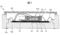
- a plastic package or the like can be used instead of the ceramic package 150 as a package in which contents such as the sensor element S1E and the IC 50 are placed. That is, any material can be used as long as it can protect contents such as the conductive wire 152 and can perform signal input / output with the outside.
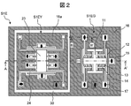
- FIG. 2 is a plan view of the sensor element S1E according to the first embodiment. For convenience, the description of the glass cap 100 described in FIG. 3 is omitted.
- the sensor element S1E has an acceleration detector S1EG and an angular velocity detector S1EY.
- the acceleration detection unit S1EG includes an inertial mass body 11, a support beam structure 12, a movable electrode 13, a fixed electrode 14, a suspension portion 15, a dummy pattern 16, and a through electrode 17.
- the inertial mass body 11 is a movable part that is displaced when an inertial force is applied to the acceleration detection part S1EG.
- the support beam structure 12 supports the inertial mass body 11.
- the movable electrode 13 is displaced together with the inertial mass body 11 to form a capacitance with the fixed electrode 14. This capacitance changes with the displacement of the inertial mass body 11, and based on this, the movement amount of the inertial mass body 11 can be detected.
- the suspension portion 15 fixes and suspends the inertial mass body 11 and the support beam structure 12 to the support layer 1a described with reference to FIG.
- the through electrode 17 penetrates the suspension portion 15 and is electrically connected to a pad 18 described later.
- the dummy pattern 16 is a portion that is arranged around the same plane of each of the above portions and does not directly contribute to the sensor function.
- the angular velocity detector S1EY includes a dummy pattern 16a, an inertial mass body 23, and a support beam structure 24.
- a gap 30 is formed between the dummy patterns 16a and 16 so that the two are electrically separated.
- the inertial mass body 23 is a movable part that is displaced when an inertial force is applied to the angular velocity detection part S1EY.
- the inertial mass body 23 can be displaced in the drive direction (x) and the detection direction (y).
- the support beam structure 24 supports the inertial mass body 23.
- the “first movable part” and the “second movable part” correspond to the inertia mass bodies 11 and 23 and the movable electrodes they have.
- the “fixed portion” corresponds to the fixed electrode 14 and a fixed electrode of the detection electrode 29 described later.
- the “first dummy part” and the “second dummy part” correspond to the dummy patterns 16 and 16a.
- the “potential generation circuit” corresponds to a circuit that supplies reference potentials 20a and 20b described later.
- FIG. 3 is a cross-sectional view of the A-A ′ plane of FIG.
- a mechanical component of the sensor element S1E such as the suspension 15 can be formed on a substrate such as an SOI (Silicon On On Insulator) substrate 1.
- SOI Silicon On On Insulator
- an intermediate insulating layer 1b is formed on the support layer 1a, and an active layer 1c is formed on the intermediate insulating layer 1b.
- the support layer 1a can be formed of, for example, silicon (Si).
- Intermediate insulating layer 1b may be formed, for example, silicon oxide (SiO 2).
- the active layer 1c can be formed of, for example, conductive silicon.
- the total thickness of the support layer 1a and the intermediate insulating layer 1b is, for example, several tens to several hundreds ⁇ m.
- the thickness of the active layer 1c is, for example, several to several tens ⁇ m.
- the SOI substrate is used in the first embodiment, the present invention is not limited to the SOI substrate, and various semiconductor substrates can be used.
- conductive polysilicon using surface MEMS technology or plating metal such as nickel (Ni) may be used as the active layer 1c.
- Each component of the composite sensor S1 according to the first embodiment is formed by processing the active layer 1c of the SOI substrate 1.
- a method for processing the active layer 1c for example, the following procedure can be considered.
- a part of the resist on the active layer 1c is removed by using photolithography or electron beam drawing technology.
- the exposed active layer 1c is removed by dry etching using RIE (Reactive Ion Etching), wet etching technology using an alkaline chemical such as TMAH (Tetra Methyl Ammonium Hydrooxide) or KOH (potassium hydroxide). To do.
- TMAH Tetra Methyl Ammonium Hydrooxide
- KOH potassium hydroxide
- the portion where the width of the active layer 1c is thin is completely free of the intermediate insulating layer 1b below, and is in a state of floating from the support layer 1a. Become.
- the intermediate insulating layer 1b below remains and is fixed to the support layer 1a.
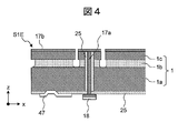
- FIG. 4 is a cross-sectional view taken along the line B-B ′ of FIG.
- a through electrode 17 is formed in the suspension portion 15.
- the through electrode 17 is connected to a pad 18 that penetrates the suspension portion 15 and is formed on the support layer 1a.
- the pad 18 is connected to the IC 50 by a conductive wire 152.
- the pad 47 is electrically connected to the support layer 1a, and a potential can be applied to the support layer 1a via the pad 47.
- the through electrode 17 can be applied with an electric signal from the support layer 1a via the pad 18 to apply a potential, or can be fixed at a constant potential.
- the through electrode 17 can be formed by the following procedure.
- the through electrode 17 can be formed.
- an electrical signal can be input / output between each component formed in the active layer 1c and the support layer 1a. Therefore, even when the cap 100 is installed on the active layer 1c using anodic bonding using glass or other adhesive, signals can be easily input / output from / to the outside of the composite sensor S1.
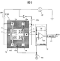
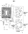
- FIG. 5 is a diagram illustrating a connection relationship between the acceleration detection unit S1EG and peripheral circuits.
- the inertial mass body 11 is displaced according to the law of inertia. The amount of displacement at this time can be calculated from the change in capacitance between the movable electrode 13 and the fixed electrode 14.
- the capacitance voltage (CV) of the IC 50 changes.
- the conversion circuit 19 converts the capacitance change into a voltage, and converts the voltage change amount into a displacement amount of the inertial mass body 11.
- the capacitance difference between the movable electrode 13 and the fixed electrode 14 can be measured by a carrier wave generated and demodulated by the carrier wave application circuit 22 and the demodulation circuit 21.
- the carrier wave uses a frequency band of several hundred kHz that the inertial mass body 11 cannot follow.
- the reason for using the high-frequency carrier wave (applying circuit) 22 is due to the following reasons (a) and (b).
- (A) The cutoff frequency of the vibration system configured as the inertial mass body 11 and the support beam structure 12 is generally 1 kHz or less, and does not follow the carrier wave 22 having a high frequency.
- the frequency of the carrier wave 22 is too high (for example, 1 MHz or more), the sensitivity of the sensor decreases due to the limitation due to the pass band of the OP-AMP 19a described later.
- the CV conversion circuit 19 includes an OP-AMP 19a and a reference capacitor Cf.
- an output Vo is obtained.
- the output Vo of the CV conversion circuit 17 satisfies the following relationship (Equation 1).
- ⁇ C Capacitance change between movable electrode 13 and fixed electrode 14
- Vc amplitude of carrier wave 22
- Vb potential 20a of positive terminal of OP-AMP 19a
- the reference potential 20a input to the plus terminal of the OP-AMP 19a constituting the CV conversion circuit 19 is also used as the reference potential of the carrier wave 22. That is, the carrier wave 22 is a signal in which the reference potential 20a is a DC voltage and an AC signal of several hundred kHz is superimposed. Since the DC components of the carrier wave 22 cancel each other during differential detection, in principle, even if there is a difference between the reference potential 20a of the OP-AMP 19a and the reference potential of the carrier wave 22, it does not affect the sensor output Vo. Absent.
- the inertial mass body 11 is caused by the difference in the reference potential 20a. Due to the displacement, an offset occurs.
- the reference potential 20b of the carrier wave 22 is the same as the reference potential 20a of the CV conversion circuit 19. Furthermore, when the power supply potential input to the sensor is Vref, the reference potentials 20a and 20b are desirably Vref / 2, that is, half of the power supply potential.
- a dummy pattern 16 is formed so as to surround the periphery of the inertial mass body 11, the support beam structure 12, the movable electrode 13, the fixed electrode 14, and the suspension portion 15.
- the main purpose of the dummy pattern 16 is to reduce the processing time when DRIE (Deep Reactive Ion Etching) of the active layer 1c, to manage the aspect ratio as uniformly as possible, and to suppress the microloading effect. Accordingly, it is intended to suppress notches whose bottom surface is excessively shaved due to overetching and conductive dust caused by black silicon.
- DRIE Deep Reactive Ion Etching
- the potential is applied to the dummy pattern 16 by connecting the pad 15 c formed on the support layer 1 a and the IC 50 with the conductive wire 152 through the through electrode 17.
- FIG. 6 is a diagram showing a connection relationship between the angular velocity detection unit S1EY and peripheral circuits.
- the angular velocity detection unit S1EY includes a drive electrode 27, a monitor electrode 28, a detection electrode 29, and a suspension unit 15 in addition to the configuration described in FIG.
- the drive electrode 27 vibrates the inertial mass body 23 in the drive direction.
- the monitor electrode 28 monitors the displacement of the inertial mass body 23 in the driving direction.
- the detection electrode 29 detects the amount of displacement when the inertial mass body 23 is displaced in the detection direction by applying an angular velocity from the outside.
- the drive signal generated by the drive circuit 32 is applied to the drive electrode 27.
- the drive electrode 27 is configured as a movable electrode provided in the inertial mass body 23 and a fixed electrode installed at a certain interval so as to face the movable electrode.
- the drive electrode 27 vibrates the inertial mass body 23 in the drive direction by an electrostatic force generated by a drive signal from the drive circuit 32.
- the effective potential difference acting on the drive electrode 27 is the potential difference between the drive signal and the reference potential of the inertial mass body 23.
- the reference potential of the inertial mass body 23 is a DC voltage 20c of a carrier wave (application circuit) 22a described later.
- the carrier wave 22a is several hundred kHz different from the carrier wave 22 for measuring the displacement of the inertial mass body 11 in order to prevent signal interference with the acceleration detector S1EG formed in the same active layer 1c.
- the carrier frequency of the band is used.
- the DC bias voltage (reference potential) 20c applied to the carrier wave 22a is the DC reference potential of the inertial mass body 23.
- an electrostatic spring effect is generated by a potential difference between a detection electrode 27 and an inertial mass body 23 described later, and the natural angular frequency in the detection direction can be adjusted. Therefore, in order to ensure a wide frequency adjustment range, the potential 20c is desirably as low as possible. In the first embodiment, it is set to about 1V.
- the Coriolis force Fc generated in the detection direction by applying the angular velocity ⁇ has the definition of (Expression 3), and the displacement y in the detection direction generated by the Coriolis force Fc has the relationship of (Expression 4). Therefore, when the sensitivity S of the angular velocity sensor is defined as the ratio of the displacement y in the detection direction to the input angular velocity ⁇ , and (Equation 3) is substituted into (Equation 4) and arranged, the sensitivity S (Equation 5) of the angular velocity sensor is obtained. It is done.
- m mass of inertial mass body
- ⁇ applied angular velocity
- v speed of inertial mass body 23 in driving direction
- the maximum sensitivity S can be obtained by matching the natural angular frequency ⁇ y of the detection vibration system to the drive angular frequency ⁇ d. Since the maximum sensitivity S means that the detected amplitude y per unit applied angular velocity is maximum, it means that the inputs to the CV conversion circuit 19 and the control IC 50 are also maximum. That is, since the displacement y which becomes a signal increases from the viewpoint of the sensor S1, the SN ratio is improved.
- the adjustment width ⁇ fy of the natural frequency fy due to the electrostatic spring effect is a function of the potential difference Vt ⁇ Vb as shown in the following (formula 6), and absorbs the variation of the natural frequency in a wider range, thereby improving the manufacturing yield.
- Vt ⁇ Vb potential difference
- the upper limit potential that can be supplied by the voltage adjustment circuit 31 is the power supply voltage Vref, in order to apply a large potential difference, it is necessary to make the reference potential 20c of the carrier wave 22a as low as possible.
- ⁇ fy Natural frequency adjustment range
- ⁇ k Spring constant adjustment amount in the detection direction of the support beam structure 24
- the potential 20a applied to the dummy pattern 16 of the acceleration detector S1EG and the potential 20c applied to the dummy pattern 16a of the angular velocity detector S1EY are not necessarily the same value.
- the active layer 1c between the acceleration detection unit S1EG and the angular velocity detection unit S1EY can be simply separated in the vertical direction, a plurality of sensor elements S1E are formed on one SOI substrate 1. Therefore, when separating each composite sensor S1 by dicing, water or dust during dicing may enter the groove, which may cause electrical leakage, which is not preferable.
- the dummy patterns 16 and 16a are electrically separated by extending the dummy pattern 16 of the acceleration detection unit S1EG into a shape surrounding the angular velocity detection unit S1EY and forming a gap 30. Since the cap 100 is hermetically sealed on the dummy pattern 16, it is possible to prevent water and dust from entering during dicing.
- the capacitance voltage (CV) conversion circuit 19 the circuit for applying the reference potentials 20a to 20d, the demodulation circuit 21, the carrier wave application circuits 22 and 22a, the voltage adjustment circuit 31, and the drive circuit 32 described with reference to FIGS. Can be formed inside.
- ⁇ Embodiment 1 Summary> As described above, in the composite sensor S1 according to the first embodiment, a plurality of movable parts that detect the amount of inertia are formed in the same layer, and the dummy patterns arranged around each movable part are electrically separated. ing. As a result, since the same potential can be applied to each movable part and the peripheral dummy pattern, a decrease in S / N ratio, an offset, and a sensitivity fluctuation caused by a potential difference between the peripheral dummy pattern and the movable part can be prevented. Can be suppressed.
- the composite sensor S1 according to the first embodiment can widen the adjustment range of the natural angular frequency variation caused by the processing error during manufacture by adjusting the reference potentials 20a and 20c. Thereby, a high yield and a reduction in manufacturing cost can be realized.
- the acceleration detection unit S1EG and the angular velocity detection unit S1EY are formed in the active layer 1c of the SOI substrate 1, and are fixed and suspended on the support layer 1a via the intermediate insulating layer 1b. . Therefore, the inertia mass bodies 11 and 23 and the support layer 1a are electrically separated from each other, and are mechanically arranged to face each other with a distance corresponding to the thickness of the intermediate insulating layer 1b. That is, like the dummy patterns 16 and 16a, it is necessary to fix the potential also in the support layer 1a.
- the support layer 1a is also positioned below the acceleration detection unit S1EG in the same manner that the dummy pattern 16 of the acceleration detection unit S1EG and the dummy pattern 16a of the angular velocity detection unit S1EY are electrically separated and applied with different potentials. It may be electrically separated into a part to be located and a part located below the angular velocity detection unit S1EY.
- the potential of the dummy pattern 16 is applied to the support layer 1a positioned below the acceleration detection unit S1EG, and the potential of the dummy pattern 16a is applied to the support layer 1a positioned below the angular velocity detection unit S1EY.
- the separation of the support layer 1a having a thickness of several hundreds of ⁇ m into two as in the second embodiment may be undesirable from the viewpoint of strength and the complexity of processing. Therefore, in the third embodiment of the present invention, the support layer 1a is not separated into two as in the second embodiment, but is set to have the same potential as the potential of the dummy pattern 16 of the acceleration detection unit S1EG. The reason will be described below.
- the detection vibration system constituting the acceleration detection unit S1EG can obtain a high sensitivity S by making the natural angular frequency ⁇ as low as possible as shown in (Expression 2).
- the natural angular frequency ⁇ should be low. Therefore, it is desirable to increase the sensitivity S and to make an overdamping design so that the mechanical cutoff frequency is lowered so as not to react to high-frequency vibration disturbances.
- the angular velocity detection unit S1EY matches the drive angular frequency ⁇ d with the natural angular frequency ⁇ y of the detection vibration system in order to obtain high sensitivity.
- the natural world there are many low-frequency vibration disturbances such as 1 / f noise and 1 / f ⁇ 2 noise. Therefore, in order to obtain an angular velocity sensor with excellent vibration resistance characteristics, it is necessary to increase the natural frequency ⁇ y of the detection vibration system as high as possible.
- the natural angular frequency of the detection vibration system of the acceleration detection unit S1EG is low, and the natural angular frequency of the angular velocity detection unit S1EY is high. It can be seen that it is preferable.
- the inertial mass body 11 of the acceleration detection unit S1EG and the inertial mass body 23 of the angular velocity detection unit S1EY are each about 30 to 100 ⁇ g, and the weight ratio is about 1: 5 at the maximum.
- these natural angular frequencies are about 6000 rad / s and 60000 rad / s, respectively, and the ratio is designed to be about 1:10. Therefore, the spring constant of the detection vibration system of the angular velocity detection unit S1EY is about 20 times or more than the spring constant of the detection vibration system of the acceleration detection unit S1EG. That is, even if there is a slight potential difference ⁇ V among the peripheral dummy pattern 16a, the support layer 1a, and the cap 100 in the angular velocity detection unit S1EY, the influence is limited.
- the DC potential is made to coincide.
- it may be adjusted to the reference potential 20a of the inertial mass body 11 having a large amount of movement due to electrostatic force between the “peripheral conductors”.
- the amount of movement due to the electrostatic force is generally the inertial mass body of the acceleration sensor.
- the dummy patterns 16 and 16a are separated and the respective potentials 20a and 20c are output to the IC 50.
- the potential generation circuit and the corresponding pad may be provided.
- the composite sensor S1 according to the third embodiment does not separate the support layer 1a, and the reference potential (20a or 20c) corresponding to the inertial mass 11 or 23 that has a larger amount of movement due to electrostatic force. Is applied. Thereby, it is possible to minimize the influence of the electrostatic force caused by the potential difference while suppressing problems related to the strength and processing difficulty of the composite sensor S1.
- the glass cap 100 containing sodium and the SOI substrate 1 are bonded together using an anodic bonding technique, but surface activated bonding, glass frit bonding, a bonding technique using a metal adhesive, or the like is used. Then, a substrate made of a conductive material such as a silicon substrate may be bonded to the SOI substrate 1.
- the cap 100 is also adjacent to the inertial mass body 11, the support beam structure 12, the movable electrode 13, and the like at a predetermined interval, and there is a possibility that an offset, a sensitivity variation, a stick, and the like are generated due to a potential difference between them.
- the potential of the cap 100 is set to the same potential as the reference potential 20a of the inertial mass body 11 like the dummy pattern 16 to prevent the above-described problems.
- the reason for matching the reference potential 20a is the same as that described in the third embodiment.
- the same potential as the dummy pattern 16 can be applied to the cap 100 by applying a conductive adhesive to the portion where the dummy pattern 16 and the cap 100 are in contact.
- a non-conductive adhesive such as a glass frit
- the sensor element S1E and the IC 50 are joined with a conductive adhesive such as silver paste.
- a potential can be applied from a potential application pad (not shown) formed on the IC 50.
- the cap 100, and the support layer 1a By applying a constant potential to the dummy pattern 16, the cap 100, and the support layer 1a, it serves as a shield for blocking electromagnetic waves from the outside, so that the reliability of the sensor S1 can be further improved.
- the composite sensor S ⁇ b> 1 applies the reference potential (20 a or 20 c) corresponding to the inertia mass bodies 11 and 23, which has the larger moving amount due to the electrostatic force, to the cap 100. Thereby, the influence of the electrostatic force caused by the potential difference can be minimized.
- the composite sensor S1 according to the fourth embodiment since all the potentials of the main components are set to the reference potential (20a or 20c), the number of wires connected to the potential generation circuit can be reduced. The circuit size can be reduced, and failures due to wire breakage can be reduced.
- the space between the cap 100 and the acceleration detection unit S1EG and the space between the cap 100 and the angular velocity detection unit S1EY are isolated, the former space is sealed with atmospheric pressure, and the latter The space may be vacuum sealed.
- the caps 100 may be provided for each of the spaces and electrically separated from each other, and each reference potential (20a or 20c) may be applied individually. Thereby, the influence of the electrostatic force caused by the potential difference can be further reduced.
- ⁇ Embodiment 6> Depending on the accuracy and application required for the composite sensor S1, it is not always necessary to separate the dummy patterns 16 and 16a, and a common potential may be applied. In this case, the potential applied to the dummy patterns 16 and 16a is applied to the inertial mass body having the larger moving amount due to the electrostatic force when a potential difference is generated between the inertial mass bodies 11 and 23 and the dummy patterns 16 and 16a. A reference potential may be used.
- the composite sensor S1 according to the present invention can be used as an inertia amount measurement and control sensor used in an automobile travel control device or a robot posture control device.
- it can be used as an inertial sensor having a plurality of inertia amounts and detection axes, which are created by using the MEMS technology and used to detect a change in capacitance.
Abstract
Description
図1は、本発明の実施形態1に係る複合センサS1の側断面図である。複合センサS1は、セラミックパッケージ150、信号処理用のIC50、センサエレメントS1Eを有する。まず、接着剤151を介してセラミックパッケージ150に信号処理用IC50を固定したあと、センサエレメントS1EをIC50上に接着固定する。その後、ワイヤボンディングを用いて、IC50、角速度センサエレメントS1E、セラミックパッケージ150の外部入出力端子154を導電性ワイヤ152で接続する。最後に蓋153で封止すると、複合センサS1が完成する。 <
FIG. 1 is a side sectional view of a composite sensor S1 according to
ΔC:可動電極13と固定電極14の間の静電容量変化分
Vc:搬送波22の振幅
Vb:OP-AMP19aのプラス端子の電位20a The
ΔC: Capacitance change between
x:加速度aが印加された時の変位量
ω:(k/m)1/2 m:慣性質量体11の質量
k:支持梁構造体のばね定数 Even if there is no processing error, the
x: displacement amount when acceleration a is applied ω: (k / m) 1/2 m: mass of inertial mass body 11 k: spring constant of support beam structure
m:慣性質量体23の質量
Ω:印加された角速度
v:慣性質量体23の駆動方向への速度 The Coriolis force Fc generated in the detection direction by applying the angular velocity Ω has the definition of (Expression 3), and the displacement y in the detection direction generated by the Coriolis force Fc has the relationship of (Expression 4). Therefore, when the sensitivity S of the angular velocity sensor is defined as the ratio of the displacement y in the detection direction to the input angular velocity Ω, and (Equation 3) is substituted into (Equation 4) and arranged, the sensitivity S (Equation 5) of the angular velocity sensor is obtained. It is done.
m: mass of inertial mass body Ω: applied angular velocity v: speed of inertial

ky:支持梁構造体24の検出方向におけるばね定数
ωd:駆動回路32から生成された駆動信号の角振動数
ωy:慣性質量体23と支持梁構造体24によって構成される検出振動系の
固有角振動数
Qy:検出振動系の機械品質係数
ky: spring constant in the detection direction of the


Δfy:固有振動数調整範囲
Δk:支持梁構造体24の検出方向におけるばね定数の調整分
ΔV=Vt-Vb
u:慣性質量体23と検出電極26との間のギャップ The adjustment width Δfy of the natural frequency fy due to the electrostatic spring effect is a function of the potential difference Vt−Vb as shown in the following (formula 6), and absorbs the variation of the natural frequency in a wider range, thereby improving the manufacturing yield. In order to achieve this, it is necessary to apply a potential difference (Vt−Vb) as large as possible. Since the upper limit potential that can be supplied by the
Δfy: Natural frequency adjustment range Δk: Spring constant adjustment amount in the detection direction of the
u: Gap between the inertial
以上のように、本実施形態1に係る複合センサS1では、慣性量を検出する複数の可動部を同一層内に形成し、各可動部の周辺に配置されたダミーパターンを電気的に分離している。これにより、各可動部と周辺ダミーパターンにはそれぞれ同電位を印加することができるので、周辺ダミーパターンと可動部の間の電位差に起因するS/N比の低下、オフセット、感度変動の発生を抑制することができる。 <Embodiment 1: Summary>
As described above, in the composite sensor S1 according to the first embodiment, a plurality of movable parts that detect the amount of inertia are formed in the same layer, and the dummy patterns arranged around each movable part are electrically separated. ing. As a result, since the same potential can be applied to each movable part and the peripheral dummy pattern, a decrease in S / N ratio, an offset, and a sensitivity fluctuation caused by a potential difference between the peripheral dummy pattern and the movable part can be prevented. Can be suppressed.
実施形態1で説明した複合センサS1において、加速度検知部S1EGと角速度検知部S1EYは、SOI基板1の活性層1c内に形成され、中間絶縁層1bを介して支持層1aに固定・懸架される。そのため、慣性質量体11および23と支持層1aの間は、電気的には分離され、機械的には中間絶縁層1bの厚さ分だけ離れた状態で対向する配置となる。すなわち、ダミーパターン16および16aと同様に、支持層1aにおいても電位を固定する必要がある。 <Embodiment 2>
In the composite sensor S1 described in the first embodiment, the acceleration detection unit S1EG and the angular velocity detection unit S1EY are formed in the
実施の形態2のように、数百μm厚さの支持層1aを2つに分離することは、強度的な観点と加工の煩雑さの観点で好ましくない場合も考えられる。そこで本発明の実施形態3では、実施形態2のように支持層1aを2つに分離せず、加速度検知部S1EGのダミーパターン16の電位と同電位になるよう設定する。以下、その理由について説明する。 <Embodiment 3>
The separation of the
以上のように、本実施形態3に係る複合センサS1は、支持層1aを分離せず、慣性質量体11および23のうち静電力による移動量が大きい方に対応する基準電位(20aまたは20c)を印加する。これにより、複合センサS1の強度や加工難度に関する問題を抑制しつつ、電位差によって生じる静電力の影響を最小限に抑えることができる。 <Embodiment 3: Summary>
As described above, the composite sensor S1 according to the third embodiment does not separate the
実施形態1~3では、陽極接合技術を用いてナトリウムを含むガラスキャップ100とSOI基板1を貼り合わせているが、表面活性化接合、ガラスフリット接合、金属接着剤を用いた接合技術などを用いて、シリコン基板など導電性材料の基板をSOI基板1に貼り合わせてもよい。この際、キャップ100も慣性質量体11、支持梁構造体12、可動電極13などと所定間隔をもって隣接することとなり、互いの電位差によるオフセット、感度変動、スティックなどが発生する可能性がある。 <Embodiment 4>
In the first to third embodiments, the
以上のように、本実施形態4に係る複合センサS1は、慣性質量体11および23のうち静電力による移動量が大きい方に対応する基準電位(20aまたは20c)をキャップ100に印加する。これにより、電位差によって生じる静電力の影響を最小限に抑えることができる。 <Embodiment 4: Summary>
As described above, the composite sensor S <b> 1 according to the fourth embodiment applies the reference potential (20 a or 20 c) corresponding to the
以上の実施形態1~4において、キャップ100および加速度検知部S1EGの間の空間と、キャップ100および角速度検知部S1EYの間の空間とを隔離し、前者の空間は大気圧封止し、後者の空間は真空封止するようにしてもよい。また、キャップ100を上記空間毎に設けた上で互いに電気的に分離し、それぞれの基準電位(20aまたは20c)を個別に印加するようにしてもよい。これにより、電位差によって生じる静電力の影響をさらに低減することができる。 <Embodiment 5>
In the above first to fourth embodiments, the space between the
複合センサS1に求められる精度や用途によっては、ダミーパターン16と16aを必ずしも分離する必要はなく、互いに共通な電位を付与してもよい。この場合、ダミーパターン16と16aに付与する電位は、慣性質量体11および23とダミーパターン16および16aの間に電位差が発生したとき、静電力による移動量が大きい方の慣性質量体に印加する基準電位を用いればよい。 <Embodiment 6>
Depending on the accuracy and application required for the composite sensor S1, it is not always necessary to separate the
S1E 複合センサのエレメント
S1EG 加速度検知部
S1EY 角速度検知部
1 SOI基板
1a 支持層
1b 中間絶縁層
1c 活性層
11 加速度検知部の慣性質量体
12 加速度検知部の支持梁構造体
13 可動電極
14 固定電極
15 固定部(懸架部)
16 加速度検知部のダミーパターン
16a 角速度検知部のダミーパターン
17 貫通電極
17a、17b ポリシリコン
18 パッド
19 容量電圧(CV)変換回路
19a OP-AMP
20a 基準電位
20b 基準電位
20c 基準電位
20d 基準電位
21 復調回路
22 搬送波印加回路
22a 搬送波印加回路
23 角速度検知部の慣性質量体
24 角速度検知部の支持梁構造体
25 酸化膜
27 駆動電極
28 モニタ電極
29 検出電極
30 ギャップ
31 電圧調整回路
32 駆動回路
47 パッド
100 キャップ
152 導電性ワイヤ
153 蓋
154 外部入出力端子 S1 Composite Sensor S1E Composite Sensor Element S1EG Acceleration Detection Unit S1EY Angular
16
20a Reference potential 20b Reference potential 20c Reference potential 20d Reference potential 21
Claims (13)
- 物理量の変化に応じて変位する第1可動部および第2可動部と、
前記第1可動部および前記第2可動部との間でそれぞれ静電容量を形成する固定部と、
前記静電容量の変化を用いて前記第1可動部の変位および前記第2可動部の変位を検出する検出部と、
前記第1可動部の周辺に配置されている第1ダミー部と、
前記第2可動部の周辺に配置されている第2ダミー部と、
前記第1可動部、前記第2可動部、前記第1ダミー部、および前記第2ダミー部に電位を印加する電位生成回路と、
を備え、
前記第1可動部、前記第2可動部、前記固定部、前記第1ダミー部、および前記第2ダミー部は、積層基板内の同一の導電層内に形成されており、
前記第1ダミー部と前記第2ダミー部は電気的に分離されており、
前記電位生成回路は、
前記第1可動部と前記第1ダミー部に第1電位を印加し、
前記第2可動部と前記第2ダミー部に第2電位を印加する
ことを特徴とする複合センサ。 A first movable part and a second movable part that are displaced according to a change in physical quantity;
A fixed part that forms capacitance between the first movable part and the second movable part,
A detection unit that detects a displacement of the first movable unit and a displacement of the second movable unit using a change in the capacitance;
A first dummy portion disposed around the first movable portion;
A second dummy portion disposed around the second movable portion;
A potential generating circuit for applying a potential to the first movable portion, the second movable portion, the first dummy portion, and the second dummy portion;
With
The first movable part, the second movable part, the fixed part, the first dummy part, and the second dummy part are formed in the same conductive layer in the multilayer substrate,
The first dummy part and the second dummy part are electrically separated;
The potential generation circuit includes:
Applying a first potential to the first movable part and the first dummy part;
A composite sensor, wherein a second potential is applied to the second movable part and the second dummy part. - 請求項1において、
前記積層基板は、支持層と、中間絶縁層と、活性層とが積層形成されてなり、
前記活性層内に、前記第1可動部、前記第2可動部、前記固定部、前記第1ダミー部、および前記第2ダミー部が形成されている
ことを特徴とする複合センサ。 In claim 1,
The laminated substrate is formed by laminating a support layer, an intermediate insulating layer, and an active layer,
The composite sensor, wherein the first movable part, the second movable part, the fixed part, the first dummy part, and the second dummy part are formed in the active layer. - 請求項2において、
前記活性層内の前記第1ダミー部と前記第2ダミー部と間の部分に配置され、前記第1ダミー部と前記第2ダミー部を電気的に分離するギャップ部を有する
ことを特徴とする複合センサ。 In claim 2,
The gap is disposed between the first dummy part and the second dummy part in the active layer, and electrically separates the first dummy part and the second dummy part. Compound sensor. - 請求項2において、
前記支持層は、
前記第1可動部の下方に配置された第1支持部と、
前記第2可動部の下方に配置された第2支持部と、
を有し、
前記第1支持部と前記第2支持部は電気的に分離されており、
前記電位生成回路は、
前記第1支持部に前記第1電位を印加し、前記第2支持部に前記第2電位を印加する
ことを特徴とする複合センサ。 In claim 2,
The support layer is
A first support portion disposed below the first movable portion;
A second support portion disposed below the second movable portion;
Have
The first support part and the second support part are electrically separated;
The potential generation circuit includes:
The composite sensor, wherein the first potential is applied to the first support portion, and the second potential is applied to the second support portion. - 請求項2において、
前記電位生成回路は、
前記第1可動部が静電力によって移動する変位量のほうが、前記第2可動部が静電力によって移動する変位量よりも大きい場合は、前記支持層に前記第1電位を印加し、
前記第2可動部が静電力によって移動する変位量のほうが、前記第1可動部が静電力によって移動する変位量よりも大きい場合は、前記支持層に前記第2電位を印加する
ことを特徴とする複合センサ。 In claim 2,
The potential generation circuit includes:
When the displacement amount that the first movable portion moves by electrostatic force is larger than the displacement amount that the second movable portion moves by electrostatic force, the first potential is applied to the support layer;
The second potential is applied to the support layer when the displacement amount by which the second movable portion moves by electrostatic force is larger than the displacement amount by which the first movable portion moves by electrostatic force. Combined sensor. - 請求項2において、
前記支持層は接地されていることを特徴とする複合センサ。 In claim 2,
The composite sensor, wherein the support layer is grounded. - 請求項1において、
前記第1可動部と前記第2可動部を覆う蓋部を備えたことを特徴とする複合センサ。 In claim 1,
A composite sensor comprising a lid that covers the first movable part and the second movable part. - 請求項7において、
前記蓋部は導電体で形成されており、
前記電位生成回路は、前記蓋部に前記第1電位または前記第2電位を印加する
ことを特徴とする複合センサ。 In claim 7,
The lid is formed of a conductor;
The composite sensor, wherein the potential generation circuit applies the first potential or the second potential to the lid. - 請求項7において、
前記蓋部は接地されていることを特徴とする複合センサ。 In claim 7,
The composite sensor, wherein the lid is grounded. - 請求項7において、
前記電位生成回路は、
前記第1可動部が静電力によって移動する変位量のほうが、前記第2可動部が静電力によって移動する変位量よりも大きい場合は、前記蓋部に前記第1電位を印加し、
前記第2可動部が静電力によって移動する変位量のほうが、前記第1可動部が静電力によって移動する変位量よりも大きい場合は、前記蓋部に前記第2電位を印加する
ことを特徴とする複合センサ。 In claim 7,
The potential generation circuit includes:
When the displacement amount that the first movable part moves by electrostatic force is larger than the displacement amount that the second movable part moves by electrostatic force, the first potential is applied to the lid part,
When the displacement amount by which the second movable part moves by electrostatic force is larger than the displacement amount by which the first movable part moves by electrostatic force, the second potential is applied to the lid portion. Combined sensor. - 請求項1において、
前記電位生成回路は、
前記第1可動部が静電力によって移動する変位量のほうが、前記第2可動部が静電力によって移動する変位量よりも大きい場合は、前記第1ダミー部と前記第2ダミー部に前記第1電位を印加し、
前記第2可動部が静電力によって移動する変位量のほうが、前記第1可動部が静電力によって移動する変位量よりも大きい場合は、前記第1ダミー部と前記第2ダミー部に前記第2電位を印加する
ことを特徴とする複合センサ。 In claim 1,
The potential generation circuit includes:
When the displacement amount by which the first movable portion is moved by electrostatic force is larger than the displacement amount by which the second movable portion is moved by electrostatic force, the first dummy portion and the second dummy portion are moved to the first dummy portion. Applying a potential,
When the displacement amount by which the second movable portion moves by electrostatic force is larger than the displacement amount by which the first movable portion moves by electrostatic force, the second dummy portion and the second dummy portion have the second displacement. A composite sensor characterized by applying an electric potential. - 請求項1において、
前記第1可動部は、
静電力によって所定の駆動方向に振動し、角速度が印加されるとコリオリ力によって前記駆動方向と直交する方向に変位する慣性体を有する、角速度検知部として構成されており、
前記第2可動部は、
角速度が印加されると変位する慣性体を有する加速度検知部として構成されている
ことを特徴とする複合センサ。 In claim 1,
The first movable part is
It is configured as an angular velocity detector having an inertial body that vibrates in a predetermined driving direction by electrostatic force and is displaced in a direction orthogonal to the driving direction by Coriolis force when an angular velocity is applied,
The second movable part is
A composite sensor characterized by being configured as an acceleration detection unit having an inertial body that is displaced when an angular velocity is applied. - 請求項12において、
前記第1可動部と前記第2可動部を覆う蓋部を備え、
前記蓋部と前記角速度検知部の間の空間は真空封止され、
前記蓋部と前記加速度検知部の間の空間は大気圧封止されている
ことを特徴とする複合センサ。 In claim 12,
A lid that covers the first movable part and the second movable part;
The space between the lid and the angular velocity detector is vacuum sealed,
A space between the lid and the acceleration detector is sealed with atmospheric pressure.
Priority Applications (2)
| Application Number | Priority Date | Filing Date | Title |
|---|---|---|---|
| DE112012000823.5T DE112012000823B4 (en) | 2011-02-16 | 2012-01-10 | Combined sensor |
| US13/983,828 US9151776B2 (en) | 2011-02-16 | 2012-01-10 | Combined sensor |
Applications Claiming Priority (2)
| Application Number | Priority Date | Filing Date | Title |
|---|---|---|---|
| JP2011030790A JP5425824B2 (en) | 2011-02-16 | 2011-02-16 | Compound sensor |
| JP2011-030790 | 2011-12-27 |
Publications (1)
| Publication Number | Publication Date |
|---|---|
| WO2012111357A1 true WO2012111357A1 (en) | 2012-08-23 |
Family
ID=46672300
Family Applications (1)
| Application Number | Title | Priority Date | Filing Date |
|---|---|---|---|
| PCT/JP2012/050214 WO2012111357A1 (en) | 2011-02-16 | 2012-01-10 | Composite sensor |
Country Status (4)
| Country | Link |
|---|---|
| US (1) | US9151776B2 (en) |
| JP (1) | JP5425824B2 (en) |
| DE (1) | DE112012000823B4 (en) |
| WO (1) | WO2012111357A1 (en) |
Cited By (1)
| Publication number | Priority date | Publication date | Assignee | Title |
|---|---|---|---|---|
| CN107923750A (en) * | 2015-08-21 | 2018-04-17 | 株式会社电装 | Compound sensor |
Families Citing this family (17)
| Publication number | Priority date | Publication date | Assignee | Title |
|---|---|---|---|---|
| JP5963567B2 (en) * | 2012-06-26 | 2016-08-03 | 日立オートモティブシステムズ株式会社 | Inertial sensor |
| JP6084473B2 (en) * | 2013-02-01 | 2017-02-22 | 日立オートモティブシステムズ株式会社 | Compound sensor |
| JP6123613B2 (en) * | 2013-09-26 | 2017-05-10 | 株式会社デンソー | Physical quantity sensor and manufacturing method thereof |
| JP6187305B2 (en) * | 2014-02-18 | 2017-08-30 | 株式会社デンソー | Gyro sensor |
| JP2015161640A (en) * | 2014-02-28 | 2015-09-07 | セイコーエプソン株式会社 | Electronic device, electronic apparatus, and moving body |
| KR101565684B1 (en) * | 2014-03-14 | 2015-11-03 | 삼성전기주식회사 | Detector module for MEMS Sensor and MEMS Sensor having the same |
| JP6451062B2 (en) | 2014-03-18 | 2019-01-16 | セイコーエプソン株式会社 | Electronic device, electronic module, electronic device, and moving object |
| JP6331535B2 (en) | 2014-03-18 | 2018-05-30 | セイコーエプソン株式会社 | Electronic devices, electronic devices, and moving objects |
| JP6380737B2 (en) * | 2014-04-18 | 2018-08-29 | セイコーエプソン株式会社 | Electronic devices, electronic devices, and moving objects |
| JP6372361B2 (en) * | 2015-01-16 | 2018-08-15 | 株式会社デンソー | Compound sensor |
| JP6572603B2 (en) * | 2015-04-13 | 2019-09-11 | セイコーエプソン株式会社 | Physical quantity sensor, electronic device and mobile object |
| US9505140B1 (en) | 2015-06-02 | 2016-11-29 | Irobot Corporation | Contact sensors for a mobile robot |
| JP6641878B2 (en) | 2015-10-21 | 2020-02-05 | セイコーエプソン株式会社 | Physical quantity sensors, electronic devices and moving objects |
| JP7155498B2 (en) * | 2017-03-29 | 2022-10-19 | セイコーエプソン株式会社 | optical filter device |
| JP6400795B1 (en) * | 2017-06-29 | 2018-10-03 | タイコエレクトロニクスジャパン合同会社 | Printed circuit board |
| JP7159548B2 (en) * | 2017-11-28 | 2022-10-25 | セイコーエプソン株式会社 | physical quantity sensors, physical quantity sensor devices, composite sensor devices, inertial measurement devices, mobile positioning devices, portable electronic devices, electronic devices and mobile objects |
| JP7456988B2 (en) * | 2021-09-15 | 2024-03-27 | 株式会社東芝 | Sensors and electrical equipment |
Citations (8)
| Publication number | Priority date | Publication date | Assignee | Title |
|---|---|---|---|---|
| JP2001091263A (en) * | 1999-09-22 | 2001-04-06 | Toyota Motor Corp | Semiconductor sensor and manufacturing method therefor |
| JP2002005950A (en) * | 2000-06-23 | 2002-01-09 | Murata Mfg Co Ltd | Combined sensor element and its manufacturing method |
| WO2004065968A1 (en) * | 2003-01-16 | 2004-08-05 | The Regents Of The University Of Michigan | Micromachined capacitive lateral accelerometer device and monolithic, three-axis accelerometer having same |
| JP2005114564A (en) * | 2003-10-08 | 2005-04-28 | Denso Corp | Semiconductor dynamic quantity sensor |
| JP2009145321A (en) * | 2007-11-19 | 2009-07-02 | Hitachi Ltd | Inertial sensor |
| JP2009168777A (en) * | 2008-01-21 | 2009-07-30 | Hitachi Ltd | Inertial sensor |
| JP2010145212A (en) * | 2008-12-18 | 2010-07-01 | Denso Corp | Semiconductor device |
| WO2010119573A1 (en) * | 2009-04-17 | 2010-10-21 | 株式会社日立製作所 | Inertial sensor and method for manufacturing the same |
Family Cites Families (7)
| Publication number | Priority date | Publication date | Assignee | Title |
|---|---|---|---|---|
| DE19530736B4 (en) * | 1995-02-10 | 2007-02-08 | Robert Bosch Gmbh | Acceleration sensor and method for manufacturing an acceleration sensor |
| JP3659160B2 (en) * | 2000-02-18 | 2005-06-15 | 株式会社デンソー | Angular velocity sensor |
| DE10060091B4 (en) * | 2000-12-02 | 2004-02-05 | Eads Deutschland Gmbh | Micromechanical inertial sensor |
| US7059190B2 (en) * | 2003-10-08 | 2006-06-13 | Denso Corporation | Semiconductor dynamic sensor having variable capacitor formed on laminated substrate |
| US7134336B2 (en) * | 2004-03-19 | 2006-11-14 | Denso Corporation | Vibration type angular velocity sensor |
| EP2060871A3 (en) * | 2007-11-19 | 2012-12-26 | Hitachi Ltd. | Inertial sensor |
| JP2010127763A (en) * | 2008-11-27 | 2010-06-10 | Hitachi Ltd | Semiconductor mechanical quantity detection sensor and controller using the same |
-
2011
- 2011-02-16 JP JP2011030790A patent/JP5425824B2/en not_active Expired - Fee Related
-
2012
- 2012-01-10 DE DE112012000823.5T patent/DE112012000823B4/en not_active Expired - Fee Related
- 2012-01-10 US US13/983,828 patent/US9151776B2/en not_active Expired - Fee Related
- 2012-01-10 WO PCT/JP2012/050214 patent/WO2012111357A1/en active Application Filing
Patent Citations (8)
| Publication number | Priority date | Publication date | Assignee | Title |
|---|---|---|---|---|
| JP2001091263A (en) * | 1999-09-22 | 2001-04-06 | Toyota Motor Corp | Semiconductor sensor and manufacturing method therefor |
| JP2002005950A (en) * | 2000-06-23 | 2002-01-09 | Murata Mfg Co Ltd | Combined sensor element and its manufacturing method |
| WO2004065968A1 (en) * | 2003-01-16 | 2004-08-05 | The Regents Of The University Of Michigan | Micromachined capacitive lateral accelerometer device and monolithic, three-axis accelerometer having same |
| JP2005114564A (en) * | 2003-10-08 | 2005-04-28 | Denso Corp | Semiconductor dynamic quantity sensor |
| JP2009145321A (en) * | 2007-11-19 | 2009-07-02 | Hitachi Ltd | Inertial sensor |
| JP2009168777A (en) * | 2008-01-21 | 2009-07-30 | Hitachi Ltd | Inertial sensor |
| JP2010145212A (en) * | 2008-12-18 | 2010-07-01 | Denso Corp | Semiconductor device |
| WO2010119573A1 (en) * | 2009-04-17 | 2010-10-21 | 株式会社日立製作所 | Inertial sensor and method for manufacturing the same |
Cited By (2)
| Publication number | Priority date | Publication date | Assignee | Title |
|---|---|---|---|---|
| CN107923750A (en) * | 2015-08-21 | 2018-04-17 | 株式会社电装 | Compound sensor |
| CN107923750B (en) * | 2015-08-21 | 2021-05-07 | 株式会社电装 | Composite sensor |
Also Published As
| Publication number | Publication date |
|---|---|
| US9151776B2 (en) | 2015-10-06 |
| JP2012168097A (en) | 2012-09-06 |
| DE112012000823T5 (en) | 2013-12-05 |
| DE112012000823B4 (en) | 2015-11-05 |
| JP5425824B2 (en) | 2014-02-26 |
| US20130312517A1 (en) | 2013-11-28 |
Similar Documents
| Publication | Publication Date | Title |
|---|---|---|
| JP5425824B2 (en) | Compound sensor | |
| US8739626B2 (en) | Micromachined inertial sensor devices | |
| JP4705229B2 (en) | Micromachining rotational angular acceleration sensor | |
| US8096180B2 (en) | Inertial sensor | |
| US9000543B2 (en) | Combined sensor | |
| JP5301767B2 (en) | Inertial sensor | |
| US9182421B2 (en) | Inertia sensor | |
| US8234920B2 (en) | Angular velocity sensor having drive member coupling beam spaced apart from drive members | |
| US20100127715A1 (en) | Semiconductor physical quantity sensor and control device using the same | |
| WO2011016859A2 (en) | Micromachined inertial sensor devices | |
| JP2012225920A (en) | Micro-electromechanical system (mems) device | |
| US9511993B2 (en) | Semiconductor physical quantity detecting sensor | |
| JP2019060794A (en) | Physical quantity measurement device, electronic apparatus and moving body | |
| WO2015115365A1 (en) | Sensor and production method for same | |
| US10338092B2 (en) | Physical quantity sensor and method for manufacturing the same | |
| JP2009145321A (en) | Inertial sensor | |
| US9568490B2 (en) | Angular velocity sensor | |
| JP2001133479A (en) | Inertia force sensor and method of manufacturing the same | |
| JPH09318656A (en) | Electrostatic capacity type acceleration sensor | |
| JP2011196966A (en) | Inertia sensor | |
| JPH10104266A (en) | Dynamic quantity sensor and integrated circuit using the same | |
| US20160091526A1 (en) | Sensor | |
| US10191078B2 (en) | Acceleration sensor | |
| KR100506073B1 (en) | A vacuum packaged microgyroscope and a fabricating method thereof | |
| WO2014208043A1 (en) | Physical quantity sensor |
Legal Events
| Date | Code | Title | Description |
|---|---|---|---|
| 121 | Ep: the epo has been informed by wipo that ep was designated in this application |
Ref document number: 12747052 Country of ref document: EP Kind code of ref document: A1 |
|
| WWE | Wipo information: entry into national phase |
Ref document number: 13983828 Country of ref document: US |
|
| WWE | Wipo information: entry into national phase |
Ref document number: 112012000823 Country of ref document: DE Ref document number: 1120120008235 Country of ref document: DE |
|
| 122 | Ep: pct application non-entry in european phase |
Ref document number: 12747052 Country of ref document: EP Kind code of ref document: A1 |