WO2012108877A1 - Organic light emitting device and materials for use in same - Google Patents
Organic light emitting device and materials for use in same Download PDFInfo
- Publication number
- WO2012108877A1 WO2012108877A1 PCT/US2011/024545 US2011024545W WO2012108877A1 WO 2012108877 A1 WO2012108877 A1 WO 2012108877A1 US 2011024545 W US2011024545 W US 2011024545W WO 2012108877 A1 WO2012108877 A1 WO 2012108877A1
- Authority
- WO
- WIPO (PCT)
- Prior art keywords
- ring
- light emitting
- phosphorescent
- group
- chemical structure
- Prior art date
Links
Classifications
-
- H—ELECTRICITY
- H10—SEMICONDUCTOR DEVICES; ELECTRIC SOLID-STATE DEVICES NOT OTHERWISE PROVIDED FOR
- H10K—ORGANIC ELECTRIC SOLID-STATE DEVICES
- H10K50/00—Organic light-emitting devices
- H10K50/10—OLEDs or polymer light-emitting diodes [PLED]
- H10K50/11—OLEDs or polymer light-emitting diodes [PLED] characterised by the electroluminescent [EL] layers
- H10K50/12—OLEDs or polymer light-emitting diodes [PLED] characterised by the electroluminescent [EL] layers comprising dopants
- H10K50/121—OLEDs or polymer light-emitting diodes [PLED] characterised by the electroluminescent [EL] layers comprising dopants for assisting energy transfer, e.g. sensitization
-
- H—ELECTRICITY
- H10—SEMICONDUCTOR DEVICES; ELECTRIC SOLID-STATE DEVICES NOT OTHERWISE PROVIDED FOR
- H10K—ORGANIC ELECTRIC SOLID-STATE DEVICES
- H10K85/00—Organic materials used in the body or electrodes of devices covered by this subclass
- H10K85/60—Organic compounds having low molecular weight
- H10K85/615—Polycyclic condensed aromatic hydrocarbons, e.g. anthracene
- H10K85/626—Polycyclic condensed aromatic hydrocarbons, e.g. anthracene containing more than one polycyclic condensed aromatic rings, e.g. bis-anthracene
-
- C—CHEMISTRY; METALLURGY
- C09—DYES; PAINTS; POLISHES; NATURAL RESINS; ADHESIVES; COMPOSITIONS NOT OTHERWISE PROVIDED FOR; APPLICATIONS OF MATERIALS NOT OTHERWISE PROVIDED FOR
- C09K—MATERIALS FOR MISCELLANEOUS APPLICATIONS, NOT PROVIDED FOR ELSEWHERE
- C09K11/00—Luminescent, e.g. electroluminescent, chemiluminescent materials
- C09K11/06—Luminescent, e.g. electroluminescent, chemiluminescent materials containing organic luminescent materials
-
- H—ELECTRICITY
- H10—SEMICONDUCTOR DEVICES; ELECTRIC SOLID-STATE DEVICES NOT OTHERWISE PROVIDED FOR
- H10K—ORGANIC ELECTRIC SOLID-STATE DEVICES
- H10K50/00—Organic light-emitting devices
- H10K50/10—OLEDs or polymer light-emitting diodes [PLED]
- H10K50/11—OLEDs or polymer light-emitting diodes [PLED] characterised by the electroluminescent [EL] layers
-
- H—ELECTRICITY
- H10—SEMICONDUCTOR DEVICES; ELECTRIC SOLID-STATE DEVICES NOT OTHERWISE PROVIDED FOR
- H10K—ORGANIC ELECTRIC SOLID-STATE DEVICES
- H10K85/00—Organic materials used in the body or electrodes of devices covered by this subclass
- H10K85/60—Organic compounds having low molecular weight
- H10K85/631—Amine compounds having at least two aryl rest on at least one amine-nitrogen atom, e.g. triphenylamine
- H10K85/636—Amine compounds having at least two aryl rest on at least one amine-nitrogen atom, e.g. triphenylamine comprising heteroaromatic hydrocarbons as substituents on the nitrogen atom
-
- H—ELECTRICITY
- H10—SEMICONDUCTOR DEVICES; ELECTRIC SOLID-STATE DEVICES NOT OTHERWISE PROVIDED FOR
- H10K—ORGANIC ELECTRIC SOLID-STATE DEVICES
- H10K85/00—Organic materials used in the body or electrodes of devices covered by this subclass
- H10K85/30—Coordination compounds
- H10K85/341—Transition metal complexes, e.g. Ru(II)polypyridine complexes
- H10K85/342—Transition metal complexes, e.g. Ru(II)polypyridine complexes comprising iridium
-
- H—ELECTRICITY
- H10—SEMICONDUCTOR DEVICES; ELECTRIC SOLID-STATE DEVICES NOT OTHERWISE PROVIDED FOR
- H10K—ORGANIC ELECTRIC SOLID-STATE DEVICES
- H10K85/00—Organic materials used in the body or electrodes of devices covered by this subclass
- H10K85/60—Organic compounds having low molecular weight
- H10K85/615—Polycyclic condensed aromatic hydrocarbons, e.g. anthracene
- H10K85/622—Polycyclic condensed aromatic hydrocarbons, e.g. anthracene containing four rings, e.g. pyrene
-
- H—ELECTRICITY
- H10—SEMICONDUCTOR DEVICES; ELECTRIC SOLID-STATE DEVICES NOT OTHERWISE PROVIDED FOR
- H10K—ORGANIC ELECTRIC SOLID-STATE DEVICES
- H10K85/00—Organic materials used in the body or electrodes of devices covered by this subclass
- H10K85/60—Organic compounds having low molecular weight
- H10K85/631—Amine compounds having at least two aryl rest on at least one amine-nitrogen atom, e.g. triphenylamine
-
- H—ELECTRICITY
- H10—SEMICONDUCTOR DEVICES; ELECTRIC SOLID-STATE DEVICES NOT OTHERWISE PROVIDED FOR
- H10K—ORGANIC ELECTRIC SOLID-STATE DEVICES
- H10K85/00—Organic materials used in the body or electrodes of devices covered by this subclass
- H10K85/60—Organic compounds having low molecular weight
- H10K85/649—Aromatic compounds comprising a hetero atom
- H10K85/657—Polycyclic condensed heteroaromatic hydrocarbons
- H10K85/6572—Polycyclic condensed heteroaromatic hydrocarbons comprising only nitrogen in the heteroaromatic polycondensed ring system, e.g. phenanthroline or carbazole
Definitions
- the present invention relates to an organic electroluminescent (EL) device such as an organic light emitting device (hereinafter abbreviated as an OLED) and materials capable of being used in such an OLED.
- an OLED organic light emitting device
- it relates to an OLED which comprises a light emitting layer which emits a red light, and materials for an OLED which are used for the same.
- OLEDs which comprise an organic thin film layer which includes a light emitting layer located between an anode and a cathode are known in the art. In such devices, emission of light may be obtained from exciton energy, produced by recombination of a hole injected into a light emitting layer with an electron.
- OLEDs are comprised of several organic layers in which at least one of the layers can be made to electroluminesce by applying a voltage across the device (see, e.g., Tang, et al, Appl. Phys. Lett. 1987, 51, 913 and Burroughes, et al, Nature, 1990, 347, 359).
- a voltage is applied across a device, the cathode effectively reduces the adjacent organic layers (i.e., injects electrons), and the anode effectively oxidizes the adjacent organic layers (i.e., injects holes).
- Holes and electrons migrate across the device toward their respective oppositely charged electrodes.
- a hole and electron meet on the same molecule recombination is said to occur, and an exciton is formed. Recombination of the hole and electron in luminescent compounds is accompanied by radiative emission, thereby producing electroluminescence.
- the exciton resulting from hole and electron recombination can have either a triplet or singlet spin state.
- Luminescence from a singlet exciton results in fluorescence
- luminescence from a triplet exciton results in phosphorescence.
- organic materials typically used in OLEDs one quarter of the excitons are singlets, and the remaining three-quarters are triplets (see, e.g., Baldo, et al, Phys. Rev. B, 1999, 60, 14422).
- phosphorescent materials that could be used to fabricate practical electro- phosphorescent OLEDs (U.S. Patent No.
- Electro-phosphorescent OLEDs have now been shown to have superior overall device efficiencies as compared with electro-fluorescent OLEDs (see, e.g., Baldo, et al, Nature, 1998, 395, 151 and Baldo, et al, Appl. Phys. Lett. 1999, 75(3), 4).
- OLEDs as described above, generally provide excellent luminous efficiency, image quality, power consumption and the ability to be incorporated into thin design products such as flat screens, and therefore hold many advantages over prior technology, such as cathode ray devices.
- OLEDs including, for example, the preparation of OLEDs having greater current efficiency are desirable.
- light emitting materials phosphorescent materials
- phosphorescent materials have been developed in which light emission is obtained from a triplet exciton in order to enhance internal quantum efficiency.
- Such OLEDs can have a theoretical internal quantum efficiency up to 100 % by using such phosphorescent materials in the light emitting layer (phosphorescent layer), and the resulting OLED will have a high efficiency and low power consumption.
- phosphorescent materials may be used as a dopant in a host material which comprises such a light emitting layer.
- excitons can efficiently be produced from a charge injected into a host material.
- Exciton energy of an exciton produced may be transferred to a dopant, and emission may be obtained from the dopant at high efficiency.
- Exitons may be formed either on the host materials or directly on the dopant.
- the excited triplet energy EgH of the host material must be greater than the excited triplet energy EgD of the phosphorescent dopant.
- an excited triplet energy Eg (T) of the host material has to be larger than an excited triplet energy Eg (S) of the phosphorescent dopant.
- CBP 4,4'-bis(N-carbazolyl)biphenyl
- CBP is known to be a representative example of a material having an efficient and large excited triplet energy. See, e.g., U.S. Patent No. 6,939,624.
- a phosphorescent dopant having a prescribed emission wavelength, such as red
- an OLED having a high efficiency can be obtained.
- the luminous efficiency is notably enhanced by phosphorescent emission.
- CBP is known to have a very short lifetime and therefore it is not suitable for practical use in EL devices such as an OLED. Without being bound by scientific theory, it is believed that this is because CBP may be heavily deteriorated by a hole due to its oxidative stability not being high, in terms of molecular structure.
- an excited singlet energy Eg (S) is larger than in a fluorescent dopant, but an excited triplet energy Eg (T) of such a host is not necessarily larger. Accordingly, a fluorescent host cannot simply be used in place of a phosphorescent host as a host material to provide a phosphorescent emitting layer.
- anthracene derivatives are known well as a fluorescent host.
- an excited state triplet energy Eg (T) of anthracene derivatives may be as small as about 1.9 eV.
- Eg (T) of anthracene derivatives may be as small as about 1.9 eV.
- energy transfer to a phosphorescent dopant having an emission wavelength in a visible light region of 500 nm to 720 nm cannot be achieved using such a host, since the excited state triplet energy would be quenched by a host having such a low triplet state energy. Accordingly, anthracene derivatives are unsuitable as a phosphorescent host.
- Perylene derivatives, pyrene derivatives and naphthacene derivatives are not preferred as phosphorescent hosts for the same reason.
- the aromatic hydrocarbon compounds described in Japanese Patent Application Laid-Open No. 142267/2003 assume a rigid molecular structure having a good symmetric property and provided with five aromatic rings in which molecules are arranged in a bilaterally symmetrical manner toward a central benzene skeleton. Such an arrangement has the drawback of a likelihood of crystallization of the light emitting layer.
- OLEDs in which various aromatic hydrocarbon compounds are used are disclosed in International Patent Application Publications WO 2007/046685; Japanese Patent Application Laid-Open No. 151966/2006; Japanese Patent Application Laid- Open No. 8588/2005; Japanese Patent Application Laid-Open No. 19219/2005; Japanese Patent Application Laid-Open No. 19219/2005; and Japanese Patent Application Laid-Open No. 75567/2004.
- the efficiency of these materials as a phosphorescent host is not disclosed.
- OLEDs prepared by using various fluorene compounds are disclosed in Japanese Patent Application Laid-Open No. 043349/2004; Japanese Patent Application Laid-Open No. 314506/2007; and Japanese Patent Application Laid-Open No. 042485/2004.
- the effectiveness of these materials as a phosphorescent host is not disclosed.
- Japanese Patent Application Laid-Open No. 042485/2004 discloses hydrocarbon compounds in which a condensed polycyclic aromatic ring is bonded directly to a fluorene ring.
- the effectiveness of an OLED prepared by combining such materials with a phosphorescent material is not disclosed, and the application discloses perylene and pyrene rings which are known to have a small triplet energy level as condensed polycyclic aromatic rings, and which are not preferred for use as a light emitting layer of a phosphorescent device, and materials which are effective for a phosphorescent device are not selected.
- phosphorescent emitter materials comprised in such OLEDs, described herein, help fulfill this objective.
- the OLEDs of the present invention are characterized by providing an organic thin film layer comprising a single layer or plural layers between a cathode and an anode, wherein the organic thin film layer comprises at least one organic light emitting layer, wherein at least one light emitting layer comprises at least one host material and at least one phosphorescent emitter material, wherein the host material comprises a substituted or unsubstituted hydrocarbon compound having the chemical structure represented by the following formula (1):
- R 2 represents a hydrogen atom, a benzene ring, a condensed aromatic hydrocarbon ring, a dibenzofuran ring or a group represented by Ar 3 -R 3 ;
- Ar 1 to Ar 3 each independently represent a benzene ring, a condensed aromatic hydrocarbon ring or a dibenzofuran ring;
- R 1 and R 3 each independently represent a hydrogen atom, a benzene ring, a condensed aromatic hydrocarbon ring, or a dibenzofuran ring;
- the condensed aromatic hydrocarbon ring represented by R 1 to R 3 and Ar 1 to Ar 3 is selected from the group consisting of a naphthalene ring, a chrysene ring, a fluoranthene ring, a triphenylene ring, a phenanthrene ring, a benzophenanthrene ring, a dibenzophenanthrene ring, a benzotriphenylene ring, a benzochrysene ring, and a benzo[b] fluoranthene ring; and R 1 to R 3 , Ar 1 to Ar 3 and 2,7- disubstituted naphthalene ring each independently may have one or more substituents; with the proviso that when Ar 1 and Ar 2 each represents a condensed aromatic hydrocarbon
- An alternative structure for the host material has the following formula (2): where Ar 4 - Ar 6 are each independently a benzene ring, fused aromatic hydrocarbon ring, or represent a dibenzofuran ring;
- R 4 , R 5 are each independently a hydrogen atom, benzene ring, fused aromatic hydrocarbon ring, or represent a dibenzofuran ring;
- R 4 , R 5 , Ar 4 - Ar 6 and fused aromatic hydrocarbon ring are each independently a naphthalene ring, chrysene ring, fluoranthene ring, triphenylene ring, phenanthrene ring, ring benzophenanthrene, or a benzophenanthrene ring, and additional structures as described below.
- the OLED comprises a host material having the chemical structure represented by the formula (RH-1):
- the phosphorescent emitter material comprises a phosphorescent organometallic complex having a substituted chemical structure represented by one of the following partial chemical structures represented by the following formulas (B-l), (B-2) and (B-3):
- each R is independently selected from the group consisting of H, alkyl, alkenyl, alkynyl, CN, CF 3 , C n F 2n+1 , trifluorovinyl, C0 2 R, C(0)R, NR 2 , N0 2 , OR, halo, aryl, heteroaryl, substituted heteroaryl or a heterocyclic group.
- the phosphorescent emitter material comprises a phosphorescent organometallic complex having a substituted chemical structure represented by the following partial chemical structure(3):
- the phosphorescent emitter material comprises a metal complex
- the metal complex comprises a metal atom selected from Ir, Pt, Os, Au, Cu, Re and Ru and a ligand.
- the metal complex has an ortho-metal bond.
- Ir is the metal atom.
- the phosphorescent emitter material comprises a phosphorescent organometallic compound having a substituted chemical structure represented by the following chemical structure (4):
- the present invention comprises an OLED which comprises a host material which comprises an unsubstituted aromatic hydrocarbon compound having the chemical structure represented by the following formula (RH-1):
- a phosphorescent emitter material which comprises a phosphorescent organometallic compound having a substituted chemical structure represented by the following chemical structure (4):
- the present invention comprises an OLED which comprises a host material which comprises an unsubstituted aromatic hydrocarbon compound having the chemical structure represented by the following formula (RH-1):
- a phosphorescent emitter material which comprises a phosphorescent organometallic compound having a substituted chemical structure represented by the following chemical structure (RD-1):
- the present invention comprises an OLED which comprises a host material, wherein the excited triplet energy of the host material is from about 2.0 eV to about 2.8 eV.
- the present invention comprises an OLED which comprises at least one phosphorescent material in the light emitting layer, wherein the phosphorescent material has a maximum value of 500 nm or more and 720 nm or less in a light emitting wavelength.
- the present invention comprises an OLED which provides improved voltage and working lifetime characteristics.
- improved characteristics of the OLEDs of the present invention may be achieved due to the serial bonding of two or more condensed poly cyclic aromatic rings to a monovalent fluorene skeleton and by bonding a group containing condensed polycyclic aromatic rings which are different from each other to a fluorene skeleton in a position in which a conjugate length is extended.
- the present invention comprises a phosphorescent OLED having high efficiency and long lifetime, which OLED comprises a material of general Formula (1) as a host material, and particularly as a phosphorescent host material.
- FIG. 1 is a drawing showing an outline constitution of one example of the OLED in the embodiment of the present invention. DETAILED DESCRIPTION
- the OLEDs of the present invention may comprise a plurality of layers located between an anode and a cathode.
- Representative OLEDs according to the invention include, but are not limited to, structures having constituent layers as described below:
- an OLED 1 comprises a transparent substrate 2, an anode 3, a cathode 4 and an organic thin film layer 10 disposed between the anode 3 and the cathode 4.
- the organic thin film layer 10 comprises a phosphorescence emitting layer 5 containing a phosphorescent host and a phosphorescent dopant, and can provide respectively a hole injecting'transporting layer 6 and the like between the phosphorescence emitting layer 5 and the anode 3, and an electron injecting'transporting layer 7 and the like between the phosphorescence emitting layer 5 and the cathode 4.
- an electron blocking layer disposed between the anode 3 and the phosphorescence emitting layer 5, and a hole blocking layer disposed between the cathode 4 and the phosphorescence emitting layer 5. This makes it possible to contain electrons and holes in the phosphorescence emitting layer 5 to enhance the production rate of excitons in the phosphorescence emitting layer 5.
- fluorescent host and "phosphorescent host” are referred to as a fluorescent host when combined with a fluorescent dopant and as a phosphorescent host when combined with a phosphorescent dopant, respectively, and should not be limited to a classification of the host material based solely on molecular structure.
- a fluorescent host in the present specification means a material constituting the fluorescence emitting layer containing a fluorescent dopant and does not mean a material which can be used only for a host of a fluorescent material.
- a phosphorescent host means a material constituting the phosphorescence emitting layer containing a phosphorescent dopant and does not mean a material which can be used only for a host of a phosphorescent material.
- a hole injecting'transporting layer means at least either one of a hole injecting layer and a hole transporting layer
- an electron injecting'transporting layer means at least either one of an electron injecting layer and an electron transporting layer
- the OLED of the present invention may be prepared on a substrate.
- the substrate referred to in this case is a substrate for supporting the OLED, and it is preferably a flat substrate in which light in the visible region of about 400 to about 700 nm has a transmittance of at least about 50 %.
- the substrate may include a glass plate, a polymer plate and the like.
- the glass plate may include soda lime glass, barium » strontium-containing glass, lead glass, aluminosilicate glass, borosilicate glass, barium borosilicate glass, quartz and the like.
- the polymer plate may include polycarbonate, acryl, polyethylene terephthalate, polyether sulfide, polysulfone and the like.
- An anode in the OLED of the present invention assumes the role of injecting a hole into the hole injecting layer, the hole transporting layer or the light emitting layer.
- the anode has a work function of 4.5 eV or more.
- a material suitable for use as the anode include indium tin oxide alloy (ITO), tin oxide (NESA), indium zinc oxide, gold, silver, platinum, copper and the like.
- ITO indium tin oxide alloy
- NESA tin oxide
- the anode can be prepared by forming a thin film from electrode substances, such as those discussed above, by a method such as a vapor deposition method, a sputtering method and the like.
- the transmittance of light in the visible light region in the anode is preferably larger than 10 %.
- the sheet resistance of the anode is preferably several hundred ⁇ /square or less.
- the film thickness of the anode is selected, depending on the material, and is typically in the range of from about 10 nm to about 1 ⁇ , and preferably from about 10 nm to about 200 nm.
- the cathode comprises preferably a material having a small work function for the purpose of injecting an electron into the electron injecting layer, the electron transporting layer or the light emitting layer.
- Materials suitable for use as the cathode include, but are not limited to indium, aluminum, magnesium, magnesium-indium alloys, magnesium-aluminum alloys, aluminum-lithium alloys, aluminum-scandium-lithium alloys, magnesium-silver alloys and the like.
- a TOLED cathode such as disclosed in U.S. Patent No. 6,548,956 is preferred.
- the cathode can be prepared, as is the case with the anode, by forming a thin film by a method such as a vapor deposition method, a sputtering method and the like.
- the light emitting layer in the OLED may be capable of carrying out the following functions singly or in combination:
- injecting function a function in which a hole can be injected from an anode or a hole injecting layer in applying an electric field and in which an electron can be injected from a cathode or an electron injecting layer;
- transporting function a function in which a charge (electron and hole) injected may be transferred by virtue of a force of an electric field
- (3) light emitting function a function in which a region for recombination of an electron and a hole may be provided, and which results in the emission of light.
- a difference may be present between ease of injection of a hole and ease of injection of an electron, and a difference may be present in the transporting ability shown by the mobilities of a hole and an electron.
- the light emitting layer is preferably a molecularly deposited film.
- the term "molecularly deposited film” means a thin film formed by depositing a compound from the gas phase and a film formed by solidifying a material compound in a solution state or a liquid phase state, and usually the above-referenced molecular deposit film can be distinguished from a thin film (molecular accumulation film) formed by an LB method by a difference in an aggregation structure and a higher order structure and a functional difference originating in it.
- the film thickness of the light emitting layer is preferably from about 5 to about 50 nm, more preferably from about 7 to about 50 nm and most preferably from about 10 to about 50 nm. If the film thickness is less than 5 nm, it is likely to be difficult to form the light emitting layer and control the chromaticity. On the other hand, if it exceeds about 50 nm, the operating voltage is likely to go up.
- an organic thin film layer comprising one layer or plural layers is provided between a cathode and an anode; the above organic thin film layer comprises at least one light emitting layer; and at least one of the organic thin film layers contains at least one phosphorescent material and at least one host material as described below. Further, at least one of the light emitting layers contains preferably at least one host material of the present invention for an organic electroluminescence device and at least one phosphorescent material.
- the light emitting layer comprises at least one phosphorescent material capable of phosphorescence emission, and a host material represented by the following formula (1):
- R 2 represents a hydrogen atom, a benzene ring, a condensed aromatic hydrocarbon ring, a dibenzofuran ring or a group represented by Ar 3 -R 3 ;
- Ar 1 to Ar 3 each independently represent a benzene ring, a condensed aromatic hydrocarbon ring or a dibenzofuran ring;
- R 1 and R 3 each independently represent a hydrogen atom, a benzene ring, a condensed aromatic hydrocarbon ring, or a dibenzofuran ring;
- the condensed aromatic hydrocarbon ring represented by R 1 to R 3 and Ar 1 to Ar 3 is selected from the group consisting of a naphthalene ring, a chrysene ring, a fluoranthene ring, a triphenylene ring, a phenanthrene ring, a benzophenanthrene ring, a dibenzophenanthrene ring, a benzotriphenylene ring, a benzochrysene ring, and a benzo[b] fluoranthene ring; and R 1 to R 3 , Ar 1 to Ar 3 and 2,7- disubstituted naphthalene ring each independently may have one or more substituents; with the proviso than when Ar 1 and Ar 2 each represents a condensed aromatic hydrocarbon
- a thin film for an OLED which demonstrates excellent stability can be formed by selecting a suitable ring structure for the host material, and using the ring structure together with a red phosphorescent material in order to provide a device having high efficiency and long lifetime.
- Anthracene derivatives which are well known fluorescent host materials, are typically unsuitable as host materials for a phosphorescent dopant for red light emission.
- the host material of the present invention has a large excited triplet energy gap and therefore makes it possible to allow a phosphorescent dopant which displays red light emission to effectively emit light.
- CBP which is well known as a phosphorescent host, functions as a host for phosphorescent dopants which have wavelengths greater than that of green light.
- the host materials of the present invention allow for light emission in phosphorescent dopants which exhibit emission at wavelengths above green light emission.
- the host material represented by the formula (1) described above provides a material which has a suitable number of ring carbon atoms and which therefore is suitable for use as a phosphorescent host for a phosphorescence emission layer having a useful light emitting wavelength and having a high stability, especially at higher operating temperatures.
- CBP and the like which have a wide excited triplet energy gap, have been used for a host material.
- CBP has a wide excited triplet energy gap Eg(T) but is associated with the problem that may have a short lifetime.
- the host material of the present invention cannot typically be applied to a host for a phosphorescent dopant having such a wide excited triplet energy gap as that of blue wavelength light, but it may function as a host for a phosphorescent dopant at wavelengths of, for example, red or green light.
- the excited triplet energy gap is wide, as is the case with CBP, the potential problem exists that intermolecular transfer of energy may not be efficiently carried out to a red phosphorescent dopant because of the large difference in energy gap.
- the energy gap maybe preferably selected in combination with red or green phosphorescent dopant, energy can efficiently be transferred to the phosphorescent dopant, and a phosphorescence emitting layer having a very high efficiency can be constituted.
- a phosphorescence emitting layer having high efficiency and long lifetime can be prepared according to the teachings of the present invention, especially a high stability at high operating temperatures.
- an excited triplet energy gap Eg(T) of the material constituting the OLED of the invention may be prescribed based on its phosphorescence emission spectrum, and it is given as an example in the present invention that the energy gap may be prescribed, as is commonly used, in the following manner.
- isopentane: ethanol 5:5:2 in terms of a volume ratio) in a concentration of 10 ⁇ /L to prepare a sample for measuring phosphorescence.
- This phosphorescence measuring sample is placed in a quartz cell and cooled to 77 K, and is subsequently irradiated with exciting light to measure the wavelength of a phosphorescence emitted.
- a tangent line is drawn based on the increase of phosphorescence emission spectrum thus obtained at the short wavelength side, and the wavelength value of the intersection point of the above tangent line and the base line is converted to an energy value, which is set as an excited triplet energy gap Eg(T).
- a commercially available measuring equipment F-4500 manufactured by Hitachi, Ltd. can be used for the measurement.
- triplet energy gap a value which can be defined as the triplet energy gap can be used without depending on the above procedure as long as it does not deviate from the scope of the present invention.
- a preferred host material has the chemical structure represented by the following formula (RH-1):
- the materials of the present invention for an organic electroluminescence device have a large triplet energy gap Eg(T) (excited triplet energy), and therefore phosphorescent light can be emitted by transferring energy to a phosphorescent dopant.
- Eg(T) excited triplet energy
- the excited triplet energy of the host material described above is preferably from about 2.0 eV to about 2.8 eV.
- the excited triplet energy of about 2.0 eV or more makes it possible to transfer energy to a phosphorescent dopant material which emits light at a wavelength of 500 nm or more and 720 nm or less.
- the excited triplet energy of about 2.8 eV or less makes it possible to avoid the problem that light emission is not efficiently carried out in a red phosphorescent dopant because of the large difference in an energy gap.
- the excited triplet energy of the host material is more preferably from about 2.1 eV to about 2.7 eV.
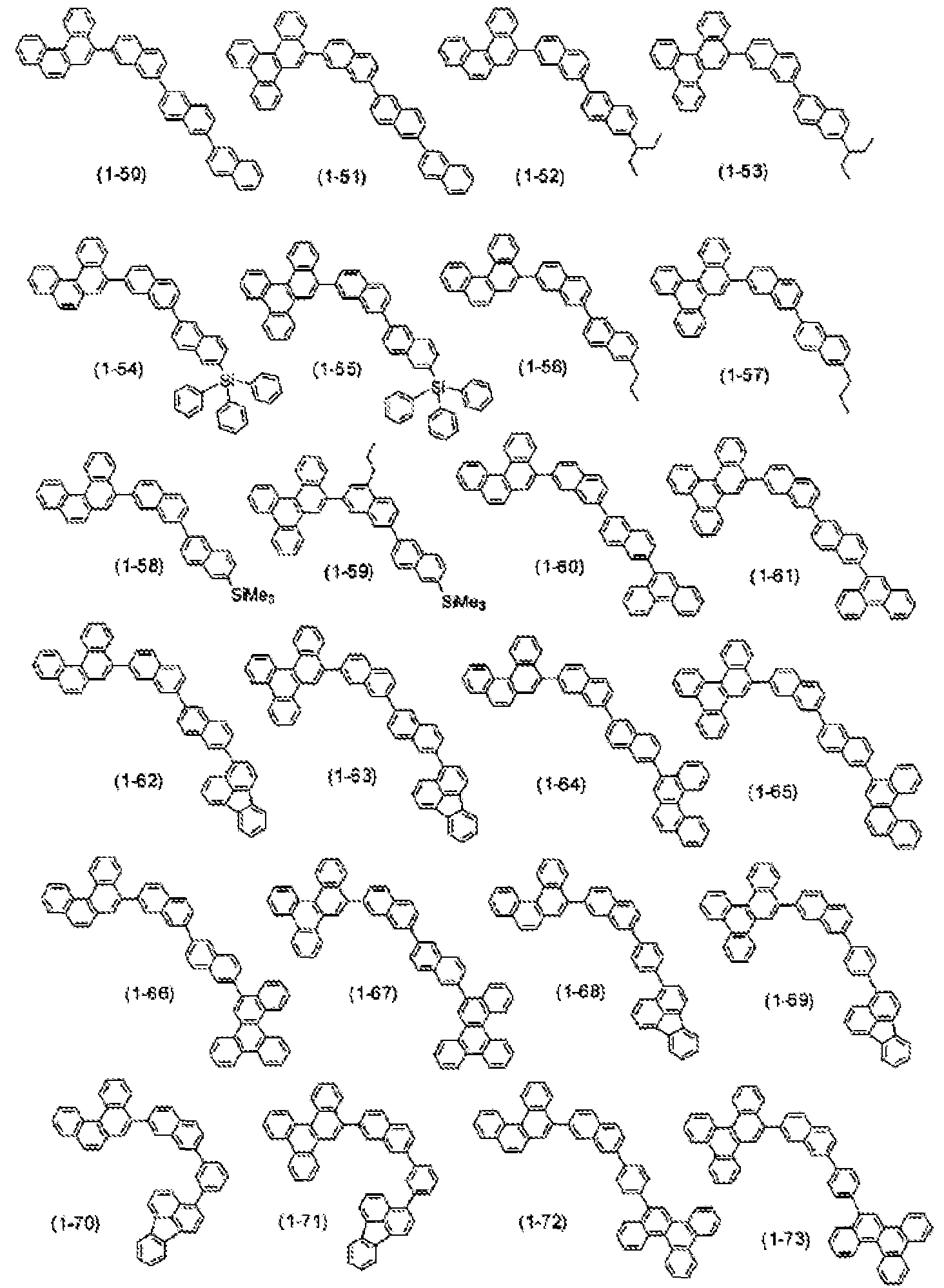
- suitable compounds for the host material accordinge present invention represented by the following formulas, include, but are not limited e following compounds:
- Ir(2-phenylquinoline) and Ir(l-phenylisoquinoline) type phosphorescent materials have been synthesized, and OLEDs incorporating them as the dopant emitters have been fabricated.
- Such devices may advantageously exhibit high current efficiency, high stability, narrow emission, high processibility (such as high solubility and low evaporation temperature), high luminous efficiency, and/or high luminous efficiency.
- the phosphorescent emitter material comprises a phosphorescent organometallic complex having a substituted chemical structure represented by one of the following partial chemical structures represented by the following formulas (B-l), (B-2) and (B-3):
- R is independently hydrogen or an alkyl substituent having 1-3 carbon atoms, and wherein at least one ring of the formula has one or more of said alkyl substituent.
- substituted structures include at least one methyl substituents, which may be substituted on any one of the rings.
- the phosphorescent organometallic complex according to the above structure may be substituted with any suitable number of methyl groups.
- the phosphorescent organometallic complex according to the above structure is substituted with at least two methyl groups.
- the phosphorescent organometallic complex according to the above structure is substituted with at least two methyl groups.
- the phosphorescent emitter material comprises a phosphorescent organometallic complex having a substituted chemical structure represented by the following partial chemical structure (3):
- the phosphorescent emitter material comprises a metal complex
- the metal complex comprises a metal atom selected from Ir, Pt, Os, Au, Cu, Re and Ru and a ligand.
- the metal complex has an ortho-metal bond.
- the metal atom is preferably Ir.
- the phosphorescent emitter material comprises a phosphorescent organometallic compound having a substituted chemical structure represented by the following chemical structure (4):
- the present invention relates to an OLED wherein the host material comprises an unsubstituted aromatic hydrocarbon compound having the chemical structure represented by the following formula (RH-1):
- the phosphorescent emitter material comprises a phosphorescent organometallic compound having a substituted chemical structure represented by the following chemical structure (RD-1):
- the OLEDs of the present invention may comprise a hole transporting layer (hole injecting layer), and the hole transporting layer (hole injecting layer) preferably contains the materials of the present invention. Also, the OLEDs of the present invention may comprise an electron transporting layer and/or a hole blocking layer, and the electron transporting layer and/or hole blocking layer preferably contains the materials of the present invention.
- the OLEDs of the present invention may contain a reductant dopant in an interlayer region between the cathode and the organic thin film layer.
- a reductant dopant in an interlayer region between the cathode and the organic thin film layer.
- Such an OLED having the described structural constitution may exhibit improved emission luminance and extended lifetime.
- the reductant dopant includes at least one dopant selected from alkali metals, alkali metal complexes, alkali metal compounds, alkali earth metals, alkali earth metal complexes, alkali earth metal compounds, rare earth metals, rare earth metal complexes, rare earth metal compounds and the like.
- Suitable alkali metals include Na (work function: 2.36 eV), K (work function: 2.28 eV), Rb (work function: 2.16 eV), Cs (work function: 1.95 eV) and the like, and the compounds having a work function of 2.9 eV or less are particularly preferred.
- K, Rb and Cs are preferred, more preferred are Rb or Cs, and even more preferred is Cs.
- the alkali earth metals include Ca (work function: 2.9 eV), Sr (work function: 2.0 to 2.5 eV), Ba (work function: 2.52 eV) and the like, and the compounds having a work function of 2.9 eV or less are particularly preferred.
- the rare earth metals include Sc, Y, Ce, Tb, Yb and the like, and the compounds having a work function of 2.9 eV or less are particularly preferred.
- metals described above it is preferred to select metals having a high reducing ability, and addition of a relatively small amount thereof to the electron injecting region may make it possible to enhance the emission luminance and extend the lifetime of the OLED.
- the alkali metal compounds include alkali metal oxides such as Li 2 0, CS2O, K2O and the like and alkali metal halides such as LiF, NaF, CsF, KF and the like.
- Preferred compounds include LiF, Li 2 0 and NaF.
- the alkali earth metal compounds include BaO, SrO, CaO and Ba x Sri_ x O (0 ⁇ x ⁇ l), Ba x Cai_ x O (0 ⁇ x ⁇ l) and the like which are obtained by mixing the above compounds, and BaO, SrO and CaO are preferred.
- the rare earth metals compound include YbF 3 , ScF 3 , SCO 3 , Y2O 3 , Ce 2 0 3 , GdF 3 , TbF 3 and the like, and YbF 3 , ScF 3 and TbF 3 are preferred.
- the alkali metal complex, the alkali earth metal complex and the rare earth metal complex shall not specifically be restricted as long as they contain at least one metal ion of alkali metal ions, alkali earth metal ions and rare earth metal ions.
- the ligand is preferably quinolinol, benzoquinolinol, acridinol, phenanthridinol, hydroxyphenyloxazole, hydroxyphenylthiazole, hydroxydiaryloxadiazole, hydroxydiarylthiadiazole,
- hydroxyfulvorane bipyridyl, phenanthroline, phthalocyanine, porphyrin, cyclopentadiene, ⁇ - diketones, azomethines and derivatives thereof.
- suitable materials are not restricted to the above-mentioned compounds.
- the reductant dopant may be formed in an interfacial region, and is preferably in a layer form or an island form.
- the forming method may be a method in which a light emitting material forming an interfacial region and an organic substance corresponding to an electron injecting material are deposited at the same time while depositing the reductant dopant by a resistance heating vapor deposition method to thereby disperse the reductant dopant in the organic substance.
- the dispersion concentration has a ratio of organic substance to reductant dopant of from about 100: 1 to 1 : 100, and preferably from about 5: 1 to 1 :5 in terms of the mole ratio.
- the reductant dopant When the reductant dopant is formed in a layer form, the light emitting material which is an organic layer in an interfacial region and the electron injecting material are formed in a layer form, and then the reductant dopant may be deposited alone by the resistance heating vapor deposition method to form the layer preferably in a thickness of 0.1 to 15 nm.
- the reductant dopant is formed in an island form
- the light emitting material which is an organic layer in an interfacial region and the electron injecting material are formed in an island form, and then the reductant dopant may be deposited alone by the resistance heating vapor deposition light emitting method to form the island preferably in a thickness of 0.05 to 1 nm.
- the OLEDs of the present invention preferably have an electron injecting layer between the light emitting layer and the cathode.
- the electron injecting layer may be a layer which functions as an electron transporting layer.
- the electron injecting layer or the electron transporting layer is a layer for assisting injection of an electron into the light emitting layer, and it has a large electron mobility.
- the electron injecting layer is provided to control an energy level including relaxation of a sudden change in the energy level.
- the forming methods of the respective layers in the OLEDs of the present invention shall not specifically be restricted, and forming methods carried out by a vacuum vapor deposition method, a spin coating method and the like which have so far publicly been known can be used.
- the organic thin film layer containing the host material compounds represented by the formula (1) described above which is used for the OLEDs of the present invention can be formed by known methods such as by vacuum vapor deposition, molecular beam evaporation (MBE method), and coating methods such as dipping, spin coating, casting, bar coating and roll coating, each using a solution prepared by dissolving the compound in a solvent.
- film thicknesses of the respective organic layers in the OLEDs of the present invention shall not specifically be restricted. In general, too small film thicknesses may be associated with defects such as pinholes and the like, while too large film thicknesses require application of high voltage, and may lower the OLED's efficiency. Accordingly, film thicknesses are typically in the a range of one to several nm to 1 ⁇ .
- the triplet energy level of the phosphorescent dopant and the triplet energy level of the host are properly regulated.
- an organic EL device with a high efficiency and an extended lifetime is obtained.
- the fluoranthene derivative is particularly effective for an extended lifetime. As compared with fluoranthene, the fluoranthene derivative has a small triplet energy level. It has been found, therefore, that the fluoranthene derivative exhibits the effect of the present invention when combined with the phosphorescent dopant of the present invention.
- the host material (1) for organic EL devices represented by the chemical formula (1) is asymmetric with respect to the 2,7-disubstituted naphthalene ring and the host material (2) for organic EL devices represented by the chemical formula (2) is asymmetric with respect to the 2,7-disubstituted naphthalene ring-Ar 5 -2,7-disubstituted naphthalene ring structure.
- the lifetimes and other performance of organic EL devices having those host materials in their light emitting layers are dramatically improved.
- each of the materials can transfer energy to a phosphorescent dopant to cause the dopant to emit phosphorescent light.
- an anthracene derivative well known as a fluorescent host is unsuitable as a host for the red light emitting phosphorescent dopant of the present invention.
- the triplet energy gap of each host materials (1) and (2) of the present invention is large, and hence the phosphorescent dopant that emits red light can be effectively caused to emit light.
- the skeleton of each material for organic EL devices is formed of a polycyclic condensed ring free of nitrogen atom, and hence the molecular stability can be improved and the lifetime of the organic EL device can be lengthened.
- the molecular stability is not sufficiently high when the number of ring atoms of the skeleton portion is excessively small.
- the conjugation system excessively extends to narrow the HOMO-LUMO gap, thereby making the triplet energy gap too small for emitting light with intended wavelength, in the red region.
- Each of the disclosed materials (1) and (2) for organic EL devices is suitable as a
- Ar 1 and Ar 2 in the host material compound formula (1) each independently represent preferably a benzene ring or the condensed aromatic hydrocarbon ring. More preferably, Ar 1 and Ar 2 represent different condensed aromatic hydrocarbon rings. In addition, Ar 1 preferably represents a ring selected from a phenanthrene ring, a fluoranthene ring, a benzophenanthrene ring, and a benzochrysene ring.
- Ar 1 is a ring selected from a phenanthrene ring, a fluoranthene ring, a benzophenanthrene ring, and a benzochrysene ring
- Ar 2 is a benzene ring or a naphthalene ring.
- Ar 4 and Ar 6 preferably each independently represent a condensed aromatic hydrocarbon ring selected from a chrysene ring, a fluoranthene ring, a benzophenanthrene ring, a dibenzophenanthrene ring, a benzotriphenylene ring, a benzochrysene ring, a benzo[b] fluoranthene ring, and a picene ring. More preferably, Ar 4 and Ar 6 are different condensed aromatic hydrocarbon rings.
- R 4 and R 5 each represent a hydrogen atom
- Ar 4 or Ar 6 represent a group selected from a phenanthrene ring, a fluoranthene ring, a benzophenanthrene ring, and a benzochrysene ring. More preferably, Ar 5 has 10 or more ring forming carbon atoms, and Ar 4 or Ar 6 represents a ring selected from a phenanthrene ring, a fluoranthene ring, a benzophenanthrene ring, and a benzochrysene ring.
- Ar 5 preferably represents a dibenzofuran ring.
- Ar 1 to Ar 3 , Ar 4 to Ar 6 each independently represent a group excellent in heat resistance, such as a substituted or unsubstituted phenanthrene ring, a substituted or unsubstituted fluoranthene ring, a substituted or unsubstituted benzophenanthrene ring, or a substituted or unsubstituted benzochrysene ring.
- Preferred examples of the one or more optional substituents for R 1 to R 3 , Ar 1 to Ar 3 , and the 2,7-disubstituted naphthalene ring in the host material formula (1), and R 4 and R 5 , Ar 4 to Ar 6 , and two 2,7-disubstituted naphthalene rings in the host material formula (2) include an aryl group having 6 to 22 carbon atoms, an alkyl group having 1 to 20 carbon atoms, a haloalkyl group having 1 to 20 carbon atoms, a cycloalkyl group having 5 to 18 carbon atoms, an unsubstituted or a substituted silyl group having 3 to 20 carbon atoms, a cyano group, and a halogen atom, with an aryl group having 6 to 14 carbon atoms exclusive of an anthracene ring, an alkyl group having 1 to 20 carbon atoms, a haloalkyl group having 1 to
- the number of substituents of R 1 to R 3 , Ar 1 to Ar 3 , and the 2,7- disubstituted naphthalene ring in the host formula (1), and R 4 , R 5 , Ar 4 to Ar 6 , and two 2,7- disubstituted naphthalene rings in the host formula (2) is preferably 2 or less, and more preferably 1 or less.
- Preferred examples of the aryl substituent having 6 to 22 carbon atoms include phenyl group, biphenyl group, terphenyl group, naphthyl group, phenylnaphthyl group, naphthylphenyl group, naphthylnaphthyl group, phenylphenanthrenyl group, chrysenyl group, fluoranthenyl group, 9,10-dialkylfluorenyl group, 9, 10-diarylfluorenyl group, triphenylenyl group, phenanthrenyl group, benzophenanthrenyl group, dibenzophenanthrenyl group, benzotriphenylenyl group, benzochrysenyl group, and dibenzofuranyl group, with an aryl group having 6 to 18 carbon atoms, such as phenyl group, biphenyl group, terphenyl group, naphthyl group, chrysenyl group,
- alkyl group having 1 to 20 carbon atoms examples include a methyl group, ethyl group, propyl group, isopropyl group, n-butyl group, s-butyl group, isobutyl group, t-butyl group, n-pentyl group, n-hexyl group, n-heptyl group, n-octyl group, n-nonyl group, n-decyl group, n-undecyl group, n-dodecyl group, n-tridecyl group, n-tetradecyl group, n-pentadecyl group, n-hexadecyl group, n-heptadecyl group, n-octadecyl group, neopentyl group, 1 -methylpentyl group, 2-methylpentyl group, 1-pentylhexyl group,
- haloalkyl group having 1 to 20 carbon atoms examples include chloromethyl group, 1 -chloroethyl group, 2-chloroethyl group, 2-chloroisobutyl group, 1,2- dichloroethyl group, 1,3-dichloroisopropyl group, 2,3-dichloro-t-butyl group, 1,2,3- trichloropropyl group, bromomethyl group, 1-bromoethyl group, 2-bromoethyl group, 2- bromoisobutyl group, 1 ,2-dibromoethyl group, 1,3-dibromoisopropyl group, 2,3-dibromo-t- butyl group, 1,2,3-tribromopropyl group, iodomethyl group, 1-iodoethyl group, 2-iodoethyl group, 2-iodoisobutyl group, 1 ,2-d
- Examples of the cycloalkyl group having 5 to 18 carbon atoms include cyclopentyl group, cyclohexyl group, cyclooctyl group, and 3,5-tetramethylcyclohexyl group, with cyclohexyl group, cyclooctyl group, and 3,5-tetramethylcyclohexyl group being preferred.
- the silyl group having 3 to 20 carbon atoms may preferably include an alkylsilyl group, an arylsilyl group, and an aralkylsilyl group.
- Examples thereof include trimethylsilyl group, triethylsilyl group, tributylsilyl group, trioctylsilyl group, triisobutylsilyl group, dimethylethylsilyl group, an unsubstituted or a dimethylisopropylsilyl group, dimethylpropylsilyl group, dimethylbutylsilyl group, dimethyl-t-butylsilyl group, diethylisopropylsilyl group, phenyldimethylsilyl group, diphenylmethylsilyl group, diphenyl- t-butylsilyl group, and triphenylsilyl group.
- the halogen atom include fluorine atom, chlorine atom, bromine atom, and
- Ar 3 in the host formula (1) is preferably a ring selected from a substituted or unsubstituted phenanthrene ring, a substituted or unsubstituted fluoranthene ring, and a substituted or unsubstituted benzophenanthrene ring.
- electroluminescence devices excellent in stability can be formed, and particularly, a high- efficiency, long-lifetime device is obtained when combinedly used with a red phosphorescent material.
- the host materials (1) and (2) for organic EL devices of the present invention preferably have excited triplet energy of 2.0 eV or more and 2.8 eV or less. If being 2.0 eV or more, the energy can be transferred to a phosphorescent light emitting material that emits light having a wavelength of 520 nm or more and 720 nm or less. If being 2.8 eV or less, the problem of inefficient light emission due to an excessively large difference in energy gap with respect to a red phosphorescent dopant can be avoided.
- the excited triplet energy of the host materials (1) and (2) is more preferably 2.0 eV or more and 2.7 eV or less, and still more preferably 2.1 eV or more and 2.7 eV or less.
- the present invention further provides an organic electroluminescence device which has an organic thin film layer with one or more layers between a cathode and an anode, in which the organic thin film layer contains the disclosed host material (1) or material (2) and at least one kind of a phosphorescent light emitting material.
- a glass substrate (size: 25 mm x 75 mm x 1.1 mm) having an ITO transparent electrode (manufactured by Geomatec Co., Ltd.) was ultrasonic-cleaned in isopropyl alcohol for five minutes, and then UV (Ultraviolet)/ozone-cleaned for 30 minutes.
- the glass substrate was mounted on a substrate holder of a vacuum deposition apparatus.
- a hole transporting layer was initially formed by vapor-depositing HT-1 in a thickness of 50 nm to cover a surface of the glass substrate where the transparent electrode lines were provided.
- a red phosphorescent-emitting layer was obtained by co-depositing RH-1 as a red phosphorescent host and RD-1 as a red phosphorescent dopant onto the hole transporting layer in a thickness of 40 nm.
- the concentration of RD-1 was 8 wt%.
- HT-1 and ET-1 are as follows:
- An organic EL device was prepared in the same manner as Example 1 except that CBP (4,4'-bis( -carbazolyl)biphenyl) was used instead of RH-1 as the red phosphorescent host and Ir(piq)3 was used instead of RD-1 as the red phosphorescent dopant.
- An organic EL device was prepared in the same manner as Example 1 except that Ir(piq)3 was used instead of RD-1 as the red phosphorescent dopant.
- Example 1 The organic EL devices each manufactured in Example 1 and Comparative Examples 1 to 3 were driven by direct-current electricity of 1 mA/cm 2 to emit light, to measure the emission chromaticity, the luminescence (L) and the voltage. Using the measured values, the current efficiency (L/J) and the luminance efficiency ⁇ (lm/W) were obtained. The results are shown in Table 2.
Landscapes
- Physics & Mathematics (AREA)
- Chemical & Material Sciences (AREA)
- Engineering & Computer Science (AREA)
- Materials Engineering (AREA)
- Spectroscopy & Molecular Physics (AREA)
- Optics & Photonics (AREA)
- Organic Chemistry (AREA)
- Electroluminescent Light Sources (AREA)
- Organic Low-Molecular-Weight Compounds And Preparation Thereof (AREA)
- Low-Molecular Organic Synthesis Reactions Using Catalysts (AREA)
Abstract
Description


Claims


Priority Applications (5)
| Application Number | Priority Date | Filing Date | Title |
|---|---|---|---|
| PCT/US2011/024545 WO2012108877A1 (en) | 2011-02-11 | 2011-02-11 | Organic light emitting device and materials for use in same |
| JP2013553409A JP2014511025A (en) | 2011-02-11 | 2011-02-11 | ORGANIC LIGHT EMITTING DEVICE AND MATERIAL FOR USE IN THE ORGANIC LIGHT EMITTING DEVICE |
| KR1020137017387A KR20140038925A (en) | 2011-02-11 | 2011-02-11 | Organic light emitting device and materials for use in same |
| US13/995,193 US20130306960A1 (en) | 2011-02-11 | 2011-02-11 | Organic light emitting device and materials for use in same |
| TW101101941A TW201233774A (en) | 2011-02-11 | 2012-01-18 | Organic light emitting device and materials for use in same |
Applications Claiming Priority (1)
| Application Number | Priority Date | Filing Date | Title |
|---|---|---|---|
| PCT/US2011/024545 WO2012108877A1 (en) | 2011-02-11 | 2011-02-11 | Organic light emitting device and materials for use in same |
Publications (2)
| Publication Number | Publication Date |
|---|---|
| WO2012108877A1 true WO2012108877A1 (en) | 2012-08-16 |
| WO2012108877A8 WO2012108877A8 (en) | 2013-06-13 |
Family
ID=44625207
Family Applications (1)
| Application Number | Title | Priority Date | Filing Date |
|---|---|---|---|
| PCT/US2011/024545 WO2012108877A1 (en) | 2011-02-11 | 2011-02-11 | Organic light emitting device and materials for use in same |
Country Status (5)
| Country | Link |
|---|---|
| US (1) | US20130306960A1 (en) |
| JP (1) | JP2014511025A (en) |
| KR (1) | KR20140038925A (en) |
| TW (1) | TW201233774A (en) |
| WO (1) | WO2012108877A1 (en) |
Cited By (1)
| Publication number | Priority date | Publication date | Assignee | Title |
|---|---|---|---|---|
| WO2020215564A1 (en) * | 2019-04-22 | 2020-10-29 | 吉林奥来德光电材料股份有限公司 | Organic light-emitting material and preparation method and application thereof |
Families Citing this family (2)
| Publication number | Priority date | Publication date | Assignee | Title |
|---|---|---|---|---|
| KR102314735B1 (en) | 2014-07-24 | 2021-10-21 | 삼성디스플레이 주식회사 | Organic light emitting device and display having the same |
| WO2017071791A1 (en) * | 2015-10-27 | 2017-05-04 | Merck Patent Gmbh | Materials for organic electroluminescent devices |
Citations (21)
| Publication number | Priority date | Publication date | Assignee | Title |
|---|---|---|---|---|
| US6303238B1 (en) | 1997-12-01 | 2001-10-16 | The Trustees Of Princeton University | OLEDs doped with phosphorescent compounds |
| US6548956B2 (en) | 1994-12-13 | 2003-04-15 | The Trustees Of Princeton University | Transparent contacts for organic devices |
| JP2003142267A (en) | 2001-08-24 | 2003-05-16 | Konica Corp | Material for organic electroluminescent element, electroluminescent element using the same, and display device |
| JP2004043349A (en) | 2002-07-11 | 2004-02-12 | Mitsui Chemicals Inc | Hydrocarbon compound, material for organic electroluminescent element and organic electroluminescent element |
| JP2004042485A (en) | 2002-07-12 | 2004-02-12 | Mitsui Chemicals Inc | Optical recording medium and hydrocarbon compound |
| JP2004075567A (en) | 2002-08-12 | 2004-03-11 | Idemitsu Kosan Co Ltd | Oligoarylene derivative and organic electroluminescent element using the same |
| US6830828B2 (en) | 1998-09-14 | 2004-12-14 | The Trustees Of Princeton University | Organometallic complexes as phosphorescent emitters in organic LEDs |
| US6835469B2 (en) | 2001-10-17 | 2004-12-28 | The University Of Southern California | Phosphorescent compounds and devices comprising the same |
| JP2005008588A (en) | 2003-06-20 | 2005-01-13 | Sony Corp | Quarter naphthyl and method for producing the same |
| JP2005019219A (en) | 2003-06-26 | 2005-01-20 | Sony Corp | Organic el light emitting element |
| US6911271B1 (en) | 2000-08-11 | 2005-06-28 | The University Of Southern California | Organometallic platinum complexes for phosphorescence based organic light emitting devices |
| US6939624B2 (en) | 2000-08-11 | 2005-09-06 | Universal Display Corporation | Organometallic compounds and emission-shifting organic electrophosphorescence |
| WO2005112519A1 (en) | 2004-05-14 | 2005-11-24 | Idemitsu Kosan Co., Ltd. | Organic electroluminescent device |
| US7001536B2 (en) | 1999-03-23 | 2006-02-21 | The Trustees Of Princeton University | Organometallic complexes as phosphorescent emitters in organic LEDs |
| JP2006151966A (en) | 2004-10-29 | 2006-06-15 | Semiconductor Energy Lab Co Ltd | Oligonaphthalene derivative, light-emitting element using oligonaphthalene derivative, and light-emitting apparatus |
| US20060204785A1 (en) | 2005-03-08 | 2006-09-14 | Kim Jung K | Red phosphorescene compounds and organic electroluminescence device using the same |
| US20060202194A1 (en) | 2005-03-08 | 2006-09-14 | Jeong Hyun C | Red phosphorescene compounds and organic electroluminescence device using the same |
| WO2007046685A1 (en) | 2005-10-17 | 2007-04-26 | Universiti Putra Malaysia | Starter kit for the production of pure and high quality microalgae |
| JP2007314506A (en) | 2006-04-27 | 2007-12-06 | Canon Inc | 4-aryl fluorene compound and organic light-emitting device using the same |
| US20080224603A1 (en) * | 2007-03-12 | 2008-09-18 | Canon Kabushiki Kaisha | Naphthalene compound and organic light-emitting device using the compound |
| WO2010076878A1 (en) * | 2009-01-05 | 2010-07-08 | 出光興産株式会社 | Organic electroluminescent element material and organic electroluminescent element comprising same |
Family Cites Families (6)
| Publication number | Priority date | Publication date | Assignee | Title |
|---|---|---|---|---|
| KR101634508B1 (en) * | 2007-03-08 | 2016-06-28 | 유니버셜 디스플레이 코포레이션 | Phosphorescent materials |
| JP2009147324A (en) * | 2007-11-22 | 2009-07-02 | Idemitsu Kosan Co Ltd | Organic el element and solution containing organic el material |
| TWI482756B (en) * | 2008-09-16 | 2015-05-01 | Universal Display Corp | Phosphorescent materials |
| CN102203975B (en) * | 2008-10-23 | 2014-04-30 | 通用显示公司 | Organic light emitting device and material used therein |
| JP4590020B1 (en) * | 2009-07-31 | 2010-12-01 | 富士フイルム株式会社 | Charge transport material and organic electroluminescent device |
| JP4617393B1 (en) * | 2010-01-15 | 2011-01-26 | 富士フイルム株式会社 | Organic electroluminescence device |
-
2011
- 2011-02-11 WO PCT/US2011/024545 patent/WO2012108877A1/en active Application Filing
- 2011-02-11 US US13/995,193 patent/US20130306960A1/en not_active Abandoned
- 2011-02-11 JP JP2013553409A patent/JP2014511025A/en active Pending
- 2011-02-11 KR KR1020137017387A patent/KR20140038925A/en not_active Application Discontinuation
-
2012
- 2012-01-18 TW TW101101941A patent/TW201233774A/en unknown
Patent Citations (22)
| Publication number | Priority date | Publication date | Assignee | Title |
|---|---|---|---|---|
| US6548956B2 (en) | 1994-12-13 | 2003-04-15 | The Trustees Of Princeton University | Transparent contacts for organic devices |
| US6303238B1 (en) | 1997-12-01 | 2001-10-16 | The Trustees Of Princeton University | OLEDs doped with phosphorescent compounds |
| US6830828B2 (en) | 1998-09-14 | 2004-12-14 | The Trustees Of Princeton University | Organometallic complexes as phosphorescent emitters in organic LEDs |
| US6902830B2 (en) | 1998-09-14 | 2005-06-07 | The Trustees Of Princeton University | Organometallic complexes as phosphorescent emitters in organic LEDs |
| US7001536B2 (en) | 1999-03-23 | 2006-02-21 | The Trustees Of Princeton University | Organometallic complexes as phosphorescent emitters in organic LEDs |
| US6911271B1 (en) | 2000-08-11 | 2005-06-28 | The University Of Southern California | Organometallic platinum complexes for phosphorescence based organic light emitting devices |
| US6939624B2 (en) | 2000-08-11 | 2005-09-06 | Universal Display Corporation | Organometallic compounds and emission-shifting organic electrophosphorescence |
| JP2003142267A (en) | 2001-08-24 | 2003-05-16 | Konica Corp | Material for organic electroluminescent element, electroluminescent element using the same, and display device |
| US6835469B2 (en) | 2001-10-17 | 2004-12-28 | The University Of Southern California | Phosphorescent compounds and devices comprising the same |
| JP2004043349A (en) | 2002-07-11 | 2004-02-12 | Mitsui Chemicals Inc | Hydrocarbon compound, material for organic electroluminescent element and organic electroluminescent element |
| JP2004042485A (en) | 2002-07-12 | 2004-02-12 | Mitsui Chemicals Inc | Optical recording medium and hydrocarbon compound |
| JP2004075567A (en) | 2002-08-12 | 2004-03-11 | Idemitsu Kosan Co Ltd | Oligoarylene derivative and organic electroluminescent element using the same |
| JP2005008588A (en) | 2003-06-20 | 2005-01-13 | Sony Corp | Quarter naphthyl and method for producing the same |
| JP2005019219A (en) | 2003-06-26 | 2005-01-20 | Sony Corp | Organic el light emitting element |
| WO2005112519A1 (en) | 2004-05-14 | 2005-11-24 | Idemitsu Kosan Co., Ltd. | Organic electroluminescent device |
| JP2006151966A (en) | 2004-10-29 | 2006-06-15 | Semiconductor Energy Lab Co Ltd | Oligonaphthalene derivative, light-emitting element using oligonaphthalene derivative, and light-emitting apparatus |
| US20060204785A1 (en) | 2005-03-08 | 2006-09-14 | Kim Jung K | Red phosphorescene compounds and organic electroluminescence device using the same |
| US20060202194A1 (en) | 2005-03-08 | 2006-09-14 | Jeong Hyun C | Red phosphorescene compounds and organic electroluminescence device using the same |
| WO2007046685A1 (en) | 2005-10-17 | 2007-04-26 | Universiti Putra Malaysia | Starter kit for the production of pure and high quality microalgae |
| JP2007314506A (en) | 2006-04-27 | 2007-12-06 | Canon Inc | 4-aryl fluorene compound and organic light-emitting device using the same |
| US20080224603A1 (en) * | 2007-03-12 | 2008-09-18 | Canon Kabushiki Kaisha | Naphthalene compound and organic light-emitting device using the compound |
| WO2010076878A1 (en) * | 2009-01-05 | 2010-07-08 | 出光興産株式会社 | Organic electroluminescent element material and organic electroluminescent element comprising same |
Non-Patent Citations (8)
| Title |
|---|
| ADACHI ET AL., APPL. PHYS. LETT., vol. 77, 2000, pages 904 |
| BALDO ET AL., APPL. PHYS. LETT., vol. 75, no. 3, 1999, pages 4 |
| BALDO ET AL., NATURE, vol. 395, 1998, pages 151 |
| BALDO ET AL., PHYS. REV. B, vol. 60, 1999, pages 14422 |
| BURROUGHES ET AL., NATURE, vol. 347, 1990, pages 359 |
| LAMANSKY ET AL., INORGANIC CHEMISTRY, vol. 40, 2001, pages 1704 |
| LAMANSKY ET AL., J. AM. CHEM. SOC., vol. 123, 2001, pages 4304 |
| TANG ET AL., APPL. PHYS. LETT., vol. 51, 1987, pages 913 |
Cited By (1)
| Publication number | Priority date | Publication date | Assignee | Title |
|---|---|---|---|---|
| WO2020215564A1 (en) * | 2019-04-22 | 2020-10-29 | 吉林奥来德光电材料股份有限公司 | Organic light-emitting material and preparation method and application thereof |
Also Published As
| Publication number | Publication date |
|---|---|
| KR20140038925A (en) | 2014-03-31 |
| US20130306960A1 (en) | 2013-11-21 |
| TW201233774A (en) | 2012-08-16 |
| JP2014511025A (en) | 2014-05-01 |
| WO2012108877A8 (en) | 2013-06-13 |
Similar Documents
| Publication | Publication Date | Title |
|---|---|---|
| US9601708B2 (en) | Organic light emitting device and materials for use in same | |
| JP6100368B2 (en) | Biscarbazole derivative host material and green light emitter for OLED light emitting region | |
| TWI580666B (en) | Aromatic amine derivatives, organic electroluminescent elements and electronic machines | |
| JP6357422B2 (en) | Organic electroluminescence device | |
| WO2014097711A1 (en) | Organic electroluminescent element and electronic device | |
| US9985232B2 (en) | Biscarbazole derivative host materials for OLED emissive region | |
| JP6133583B2 (en) | Organic electroluminescence device | |
| JP4947142B2 (en) | Light emitting device material and light emitting device | |
| KR20190014600A (en) | Light-emitting element | |
| TW201219539A (en) | Monoamine derivative and organic electroluminescent element using same | |
| TW201708209A (en) | Novel compound and organic electroluminescent device comprising same | |
| JP6376727B2 (en) | Organic electroluminescence device and electronic device | |
| TW201114320A (en) | Organic electroluminescent element | |
| US8941099B2 (en) | Organic light emitting device and materials for use in same | |
| US20130306960A1 (en) | Organic light emitting device and materials for use in same | |
| TW201718446A (en) | Organic compound and organic electroluminescence device using the same | |
| TWI589564B (en) | Organic light emitting device and materials for use in same | |
| WO2022131123A1 (en) | Organic electroluminescent element and method for manufacturing same | |
| KR20240019325A (en) | Organic electroluminescent devices, organic electroluminescent display devices and electronic devices | |
| KR20240021855A (en) | Organic electroluminescent devices, organic electroluminescent display devices and electronic devices | |
| WO2022154029A1 (en) | Organic electroluminescent element, organic electroluminescent display device, and electronic device | |
| CN117402130A (en) | 1,3, 4-triaryl substituted dibenzofuran compound and light-emitting device thereof |
Legal Events
| Date | Code | Title | Description |
|---|---|---|---|
| 121 | Ep: the epo has been informed by wipo that ep was designated in this application |
Ref document number: 11705129 Country of ref document: EP Kind code of ref document: A1 |
|
| WWE | Wipo information: entry into national phase |
Ref document number: 13995193 Country of ref document: US |
|
| ENP | Entry into the national phase |
Ref document number: 20137017387 Country of ref document: KR Kind code of ref document: A |
|
| ENP | Entry into the national phase |
Ref document number: 2013553409 Country of ref document: JP Kind code of ref document: A |
|
| NENP | Non-entry into the national phase |
Ref country code: DE |
|
| 122 | Ep: pct application non-entry in european phase |
Ref document number: 11705129 Country of ref document: EP Kind code of ref document: A1 |