WO2012105187A1 - Capacitance-varying type power-generation element - Google Patents
Capacitance-varying type power-generation element Download PDFInfo
- Publication number
- WO2012105187A1 WO2012105187A1 PCT/JP2012/000455 JP2012000455W WO2012105187A1 WO 2012105187 A1 WO2012105187 A1 WO 2012105187A1 JP 2012000455 W JP2012000455 W JP 2012000455W WO 2012105187 A1 WO2012105187 A1 WO 2012105187A1
- Authority
- WO
- WIPO (PCT)
- Prior art keywords
- power generation
- ferroelectric
- dielectric
- polarization
- generation element
- Prior art date
Links
- 238000010248 power generation Methods 0.000 title claims abstract description 52
- 239000013078 crystal Substances 0.000 claims abstract description 26
- 229920002595 Dielectric elastomer Polymers 0.000 claims abstract description 14
- 238000010030 laminating Methods 0.000 claims abstract 3
- 230000010287 polarization Effects 0.000 claims description 77
- 239000000463 material Substances 0.000 claims description 32
- 230000008859 change Effects 0.000 claims description 22
- 229910052797 bismuth Inorganic materials 0.000 claims description 4
- JCXGWMGPZLAOME-UHFFFAOYSA-N bismuth atom Chemical compound [Bi] JCXGWMGPZLAOME-UHFFFAOYSA-N 0.000 claims description 4
- 229910052721 tungsten Inorganic materials 0.000 claims description 3
- 239000010937 tungsten Substances 0.000 claims description 3
- 239000010408 film Substances 0.000 description 18
- 238000000034 method Methods 0.000 description 16
- 229920001971 elastomer Polymers 0.000 description 14
- 239000000806 elastomer Substances 0.000 description 14
- 229910052451 lead zirconate titanate Inorganic materials 0.000 description 9
- 239000000919 ceramic Substances 0.000 description 7
- 238000006243 chemical reaction Methods 0.000 description 5
- 229920005989 resin Polymers 0.000 description 5
- 239000011347 resin Substances 0.000 description 5
- RTAQQCXQSZGOHL-UHFFFAOYSA-N Titanium Chemical compound [Ti] RTAQQCXQSZGOHL-UHFFFAOYSA-N 0.000 description 4
- 239000004020 conductor Substances 0.000 description 4
- HFGPZNIAWCZYJU-UHFFFAOYSA-N lead zirconate titanate Chemical compound [O-2].[O-2].[O-2].[O-2].[O-2].[Ti+4].[Zr+4].[Pb+2] HFGPZNIAWCZYJU-UHFFFAOYSA-N 0.000 description 4
- 239000000203 mixture Substances 0.000 description 4
- 238000004544 sputter deposition Methods 0.000 description 4
- 239000010409 thin film Substances 0.000 description 4
- YCKRFDGAMUMZLT-UHFFFAOYSA-N Fluorine atom Chemical compound [F] YCKRFDGAMUMZLT-UHFFFAOYSA-N 0.000 description 3
- 230000015572 biosynthetic process Effects 0.000 description 3
- 230000006835 compression Effects 0.000 description 3
- 238000007906 compression Methods 0.000 description 3
- 230000005621 ferroelectricity Effects 0.000 description 3
- 229910052731 fluorine Inorganic materials 0.000 description 3
- 239000011737 fluorine Substances 0.000 description 3
- 230000006698 induction Effects 0.000 description 3
- 229910010272 inorganic material Inorganic materials 0.000 description 3
- 239000011147 inorganic material Substances 0.000 description 3
- 229910052751 metal Inorganic materials 0.000 description 3
- PXHVJJICTQNCMI-UHFFFAOYSA-N nickel Substances [Ni] PXHVJJICTQNCMI-UHFFFAOYSA-N 0.000 description 3
- 238000012546 transfer Methods 0.000 description 3
- 229910002113 barium titanate Inorganic materials 0.000 description 2
- 239000003990 capacitor Substances 0.000 description 2
- 239000002131 composite material Substances 0.000 description 2
- 238000013461 design Methods 0.000 description 2
- 230000006866 deterioration Effects 0.000 description 2
- 230000000694 effects Effects 0.000 description 2
- 230000005686 electrostatic field Effects 0.000 description 2
- 239000012535 impurity Substances 0.000 description 2
- 229910052746 lanthanum Inorganic materials 0.000 description 2
- FZLIPJUXYLNCLC-UHFFFAOYSA-N lanthanum atom Chemical compound [La] FZLIPJUXYLNCLC-UHFFFAOYSA-N 0.000 description 2
- 230000028161 membrane depolarization Effects 0.000 description 2
- 239000002184 metal Substances 0.000 description 2
- 229910052759 nickel Inorganic materials 0.000 description 2
- 239000002861 polymer material Substances 0.000 description 2
- 229910052719 titanium Inorganic materials 0.000 description 2
- 241000877463 Lanio Species 0.000 description 1
- 229920000459 Nitrile rubber Polymers 0.000 description 1
- 239000004793 Polystyrene Substances 0.000 description 1
- 229910004121 SrRuO Inorganic materials 0.000 description 1
- 239000004809 Teflon Substances 0.000 description 1
- 229920006362 Teflon® Polymers 0.000 description 1
- YPQJHZKJHIBJAP-UHFFFAOYSA-N [K].[Bi] Chemical compound [K].[Bi] YPQJHZKJHIBJAP-UHFFFAOYSA-N 0.000 description 1
- WOIHABYNKOEWFG-UHFFFAOYSA-N [Sr].[Ba] Chemical compound [Sr].[Ba] WOIHABYNKOEWFG-UHFFFAOYSA-N 0.000 description 1
- 229920000800 acrylic rubber Polymers 0.000 description 1
- 239000000443 aerosol Substances 0.000 description 1
- 229910052782 aluminium Inorganic materials 0.000 description 1
- QVGXLLKOCUKJST-UHFFFAOYSA-N atomic oxygen Chemical compound [O] QVGXLLKOCUKJST-UHFFFAOYSA-N 0.000 description 1
- JRPBQTZRNDNNOP-UHFFFAOYSA-N barium titanate Chemical compound [Ba+2].[Ba+2].[O-][Ti]([O-])([O-])[O-] JRPBQTZRNDNNOP-UHFFFAOYSA-N 0.000 description 1
- 239000011230 binding agent Substances 0.000 description 1
- FSAJRXGMUISOIW-UHFFFAOYSA-N bismuth sodium Chemical compound [Na].[Bi] FSAJRXGMUISOIW-UHFFFAOYSA-N 0.000 description 1
- 229910052804 chromium Inorganic materials 0.000 description 1
- 150000001875 compounds Chemical class 0.000 description 1
- 239000011231 conductive filler Substances 0.000 description 1
- 239000000470 constituent Substances 0.000 description 1
- 230000008602 contraction Effects 0.000 description 1
- 229910052802 copper Inorganic materials 0.000 description 1
- RKTYLMNFRDHKIL-UHFFFAOYSA-N copper;5,10,15,20-tetraphenylporphyrin-22,24-diide Chemical compound [Cu+2].C1=CC(C(=C2C=CC([N-]2)=C(C=2C=CC=CC=2)C=2C=CC(N=2)=C(C=2C=CC=CC=2)C2=CC=C3[N-]2)C=2C=CC=CC=2)=NC1=C3C1=CC=CC=C1 RKTYLMNFRDHKIL-UHFFFAOYSA-N 0.000 description 1
- 238000003851 corona treatment Methods 0.000 description 1
- 230000007423 decrease Effects 0.000 description 1
- 238000000151 deposition Methods 0.000 description 1
- 239000003989 dielectric material Substances 0.000 description 1
- NKZSPGSOXYXWQA-UHFFFAOYSA-N dioxido(oxo)titanium;lead(2+) Chemical compound [Pb+2].[O-][Ti]([O-])=O NKZSPGSOXYXWQA-UHFFFAOYSA-N 0.000 description 1
- 238000009826 distribution Methods 0.000 description 1
- 230000005684 electric field Effects 0.000 description 1
- 239000007772 electrode material Substances 0.000 description 1
- 230000007613 environmental effect Effects 0.000 description 1
- 239000010419 fine particle Substances 0.000 description 1
- 229920001973 fluoroelastomer Polymers 0.000 description 1
- 238000007429 general method Methods 0.000 description 1
- 229910052737 gold Inorganic materials 0.000 description 1
- 238000001027 hydrothermal synthesis Methods 0.000 description 1
- 229910052741 iridium Inorganic materials 0.000 description 1
- 229910052742 iron Inorganic materials 0.000 description 1
- 229920003049 isoprene rubber Polymers 0.000 description 1
- 238000003475 lamination Methods 0.000 description 1
- QNZFKUWECYSYPS-UHFFFAOYSA-N lead zirconium Chemical compound [Zr].[Pb] QNZFKUWECYSYPS-UHFFFAOYSA-N 0.000 description 1
- GQYHUHYESMUTHG-UHFFFAOYSA-N lithium niobate Chemical compound [Li+].[O-][Nb](=O)=O GQYHUHYESMUTHG-UHFFFAOYSA-N 0.000 description 1
- 238000004519 manufacturing process Methods 0.000 description 1
- 239000012528 membrane Substances 0.000 description 1
- 229910044991 metal oxide Inorganic materials 0.000 description 1
- 150000004706 metal oxides Chemical class 0.000 description 1
- 238000012986 modification Methods 0.000 description 1
- 230000004048 modification Effects 0.000 description 1
- 229910052760 oxygen Inorganic materials 0.000 description 1
- 239000001301 oxygen Substances 0.000 description 1
- 125000004430 oxygen atom Chemical group O* 0.000 description 1
- 229910052697 platinum Inorganic materials 0.000 description 1
- 229920000058 polyacrylate Polymers 0.000 description 1
- 229920000642 polymer Polymers 0.000 description 1
- 229920000098 polyolefin Polymers 0.000 description 1
- 229920002223 polystyrene Polymers 0.000 description 1
- -1 polytetrafluoroethylene Polymers 0.000 description 1
- 229920001343 polytetrafluoroethylene Polymers 0.000 description 1
- 239000004810 polytetrafluoroethylene Substances 0.000 description 1
- 229920002635 polyurethane Polymers 0.000 description 1
- 239000004814 polyurethane Substances 0.000 description 1
- UKDIAJWKFXFVFG-UHFFFAOYSA-N potassium;oxido(dioxo)niobium Chemical compound [K+].[O-][Nb](=O)=O UKDIAJWKFXFVFG-UHFFFAOYSA-N 0.000 description 1
- 230000008569 process Effects 0.000 description 1
- 238000007650 screen-printing Methods 0.000 description 1
- 229920002379 silicone rubber Polymers 0.000 description 1
- 239000004945 silicone rubber Substances 0.000 description 1
- 239000011734 sodium Substances 0.000 description 1
- UYLYBEXRJGPQSH-UHFFFAOYSA-N sodium;oxido(dioxo)niobium Chemical compound [Na+].[O-][Nb](=O)=O UYLYBEXRJGPQSH-UHFFFAOYSA-N 0.000 description 1
- 230000002269 spontaneous effect Effects 0.000 description 1
- 239000000126 substance Substances 0.000 description 1
- 229920003051 synthetic elastomer Polymers 0.000 description 1
- 239000005061 synthetic rubber Substances 0.000 description 1
- 229910052715 tantalum Inorganic materials 0.000 description 1
- 229920002725 thermoplastic elastomer Polymers 0.000 description 1
- 229920001187 thermosetting polymer Polymers 0.000 description 1
- 238000007740 vapor deposition Methods 0.000 description 1
- 239000012808 vapor phase Substances 0.000 description 1
- 230000000007 visual effect Effects 0.000 description 1
- 229910052726 zirconium Inorganic materials 0.000 description 1
Images
Classifications
-
- H—ELECTRICITY
- H02—GENERATION; CONVERSION OR DISTRIBUTION OF ELECTRIC POWER
- H02N—ELECTRIC MACHINES NOT OTHERWISE PROVIDED FOR
- H02N2/00—Electric machines in general using piezoelectric effect, electrostriction or magnetostriction
- H02N2/18—Electric machines in general using piezoelectric effect, electrostriction or magnetostriction producing electrical output from mechanical input, e.g. generators
-
- H—ELECTRICITY
- H01—ELECTRIC ELEMENTS
- H01G—CAPACITORS; CAPACITORS, RECTIFIERS, DETECTORS, SWITCHING DEVICES OR LIGHT-SENSITIVE DEVICES, OF THE ELECTROLYTIC TYPE
- H01G7/00—Capacitors in which the capacitance is varied by non-mechanical means; Processes of their manufacture
- H01G7/06—Capacitors in which the capacitance is varied by non-mechanical means; Processes of their manufacture having a dielectric selected for the variation of its permittivity with applied voltage, i.e. ferroelectric capacitors
-
- H—ELECTRICITY
- H02—GENERATION; CONVERSION OR DISTRIBUTION OF ELECTRIC POWER
- H02N—ELECTRIC MACHINES NOT OTHERWISE PROVIDED FOR
- H02N1/00—Electrostatic generators or motors using a solid moving electrostatic charge carrier
- H02N1/002—Electrostatic motors
- H02N1/006—Electrostatic motors of the gap-closing type
- H02N1/008—Laterally driven motors, e.g. of the comb-drive type
-
- Y—GENERAL TAGGING OF NEW TECHNOLOGICAL DEVELOPMENTS; GENERAL TAGGING OF CROSS-SECTIONAL TECHNOLOGIES SPANNING OVER SEVERAL SECTIONS OF THE IPC; TECHNICAL SUBJECTS COVERED BY FORMER USPC CROSS-REFERENCE ART COLLECTIONS [XRACs] AND DIGESTS
- Y02—TECHNOLOGIES OR APPLICATIONS FOR MITIGATION OR ADAPTATION AGAINST CLIMATE CHANGE
- Y02T—CLIMATE CHANGE MITIGATION TECHNOLOGIES RELATED TO TRANSPORTATION
- Y02T10/00—Road transport of goods or passengers
- Y02T10/60—Other road transportation technologies with climate change mitigation effect
- Y02T10/70—Energy storage systems for electromobility, e.g. batteries
Definitions
- the present invention relates to a power generation element that generates power by a change in capacitance between electrodes.
- fluorine-based resins such as polytetrafluoroethylene, Teflon (registered trademark), and CYTOP® (registered trademark) are mainly used as dielectrics used in electrets (Patent Documents 1 to 4).
- these resin materials cannot have a very high surface charge density.
- the surface charge density of the fluorine-based resin material is generally about 0.005 ⁇ C / cm 2 , and even a high one is about 0.15 ⁇ C / cm 2 .
- Patent Document 5 proposes an electromechanical conversion element using a dielectric polarization plate made of a ferroelectric material as an electret material having a high surface charge density.
- Patent Documents 1 to 4 there is a gap between the electret material and one electrode, and electrostatic induction is induced in the electrode with relative movement (movement in the horizontal direction) between the electret material and the electrode.
- An element that performs mechanical-electrical conversion by utilizing the change in the amount of charge is disclosed.
- Patent Document 5 as an electret is inserted between capacitors, one of the capacitor electrodes is used as a vibration plate, and the electrodes are displaced by being vibrated by sound. It is disclosed that a ferroelectric material having a high surface charge density is used as an electret in an electret condenser microphone (EMC) that converts it into a signal.
- EMC electret condenser microphone
- a ferroelectric For the surface charge density of a ferroelectric material, its remanent polarization value is one measure.
- a ferroelectric has a large remanent polarization value and is considered to be 10 ⁇ C / cm 2 or more. Therefore, by using an electret made of a ferroelectric ceramic described in Patent Document 5, it is larger than a polymer material.
- the electromechanical conversion efficiency can be achieved, and it is considered that there is a certain effect in the use as a microphone. However, when utilization as a power generation element is studied, sufficient power generation efficiency has not been obtained yet.
- the present invention has been made in view of the above circumstances, and an object of the present invention is to provide a capacitance change type power generation element with high power generation efficiency.
- a capacitance change type power generating element of the present invention includes a laminate in which a dielectric polarization body and a dielectric elastomer layer are laminated, and a pair of electrodes arranged above and below in the lamination direction of the laminate,
- the dielectric polarization body is made of a ferroelectric material having crystal orientation.
- Another dielectric layer may be provided between the laminate and the electrode.
- the ferroelectric material may contain inevitable impurities.
- orientation rate F measured by the Lottgering method being 50% or more.
- the orientation rate F is represented by the following formula.
- F (%) (P ⁇ P0) / (1 ⁇ P0) ⁇ 100 (i)
- P is the ratio of the total reflection intensity from the orientation plane to the total reflection intensity.
- P is the sum ⁇ I (00l) of the reflection intensity I (00l) from the (00l) plane and the sum ⁇ I (hkl) of the reflection intensity I (hkl) from each crystal plane (hkl). ( ⁇ I (00l) / ⁇ I (hkl) ⁇ ).
- P I (001) / [I (001) + I (100) + I (101) + I (110) + I (111)].
- P0 is P of a sample having a completely random orientation.
- F 0%
- F 100%.
- the polarization axis that minimizes the relative dielectric constant of the ferroelectric material is oriented substantially parallel to the layer thickness direction.
- the dielectric polarization body preferably has a remanent polarization value of 5 ⁇ C / cm 2 or more and a relative dielectric constant of 400 or less.
- the relative dielectric constant is more preferably less than 200.
- the ferroelectric is a single crystal.
- the Young's modulus of the dielectric elastomer layer is preferably 100 MPa or less, and more preferably 10 MPa or less.
- the crystal structure of the ferroelectric material is preferably a perovskite structure, a bismuth layer structure, or a tungsten bronze structure, and the ferroelectric material mainly contains a perovskite oxide that does not contain lead. preferable.
- a perovskite oxide a bismuth-containing perovskite oxide is preferable.
- the electrostatic capacity change type power generating element of the present invention uses a ferroelectric material having crystal orientation as a dielectric polarization body. According to such a configuration, a ferroelectric material having a large remanent polarization value is further oriented to form a dielectric polarization material, thereby having a very large surface charge density.
- a dielectric elastomer is disposed between the dielectric polarization body and one of the electrodes, and the distance between the electrode and the dielectric polarization body can be greatly changed by the elasticity of the dielectric elastomer, thereby improving the amount of power generation. be able to.
- the dielectric constant of the dielectric polarization layer may be lowered. And greater power generation characteristics can be achieved.
- a configuration using an inorganic material such as a perovskite oxide as a ferroelectric provides a capacitance change type power generation element having higher heat resistance and higher power generation characteristics than a resin material. be able to.
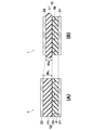
- FIG. 1 is a schematic cross-sectional view in the thickness direction showing the configuration of a capacitance change power generating element according to an embodiment of the present invention.
- FIG. 1 is a schematic cross-sectional view of a power generating element 1 according to an embodiment of the present invention, where (A) shows a state before element compression (state A), and (B) shows an element compression state (state B).
- A shows a state before element compression
- B shows an element compression state
- the scales of the constituent elements of each part are appropriately changed and shown.
- the power generating element 1 includes a laminated body 12 including a dielectric polarization body layer 10 made of a ferroelectric material having crystal orientation and a dielectric elastomer layer 11 laminated on the dielectric polarization body layer 10.
- a lower electrode 21 and an upper electrode 22 which are a pair of electrodes provided on the upper and lower surfaces of the laminate 12 are provided.
- the dielectric polarization layer 10 is made of a polarized ferroelectric layer and has a surface charge due to remanent polarization in the ferroelectric.
- the lower electrode 21 and the upper electrode 22 are electrically connected to a load (not shown), and the power generating element 1 generates electric energy by changing the capacitance by changing the distance between the electrodes 21 and 22.
- This is a capacitance change type power generating element.
- the distance between the electrodes 21 and 22 is changed in a state where charges are electrostatically induced in the electrodes 21 and 22 by the electrostatic field formed by the dielectric polarization layer 10. As the distance between the electrodes changes, an asymmetry occurs in the charge distribution, and a potential difference occurs between the electrodes. Charge transfer occurs so that this potential difference becomes 0, and this becomes a current flowing in the external circuit (load).
- the state B before the compressive force is applied to the power generating element 1 shown in FIG. 1A in the stacking direction from the state A before the compressive force shown in FIG.
- a potential difference is generated between the electrodes 21 and 22, and a function as a power generation element is obtained by taking out the change in the potential difference as electric power.
- the thickness of the elastomer layer 11 is changed by the external pressure (compression force), and the ferroelectric layer 10 is hardly changed.
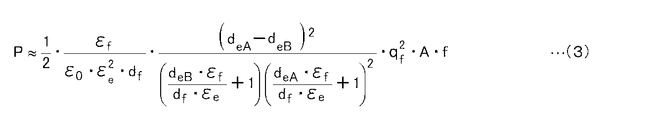
- the power generation amount P in the element of the present invention is defined by the following formula (1), where f is the frequency at which the compressive force is applied between the electrodes.
- q eA is the surface charge density of the elastomer in state A
- q eB is the surface charge density of the elastomer after charge transfer that occurs after becoming compressed state B.
- ⁇ V is the amount of change in potential difference when changing from state A to state B.
- the amount of change in potential difference is the potential difference of the elastomer layer.
- V eA is the potential of the elastomer side electrode in the state A
- ⁇ V eB is the potential of the elastomer side electrode before the charge transfer in the compressed state B.
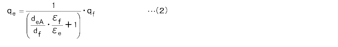
- the charge density q eA electrostatically induced on the surface of the elastomer layer by dielectric polarization by the ferroelectric layer and the charge density q f on the surface of the ferroelectric layer can be expressed by the following formula (2).
- the power generation amount P is expressed by the following expression (3).
- the dielectric polarization layer 10 has a higher surface charge density q f and a smaller relative dielectric constant ⁇ f because a higher power generation amount can be obtained. Further, the thickness d eA in the state A of the elastomeric layer, as the difference between the thickness d eB in state B (the amount of change in thickness) is large, it is also clear that the power generation amount increases.
- the lower electrode 21 is not particularly limited as long as it is a base material made of a conductor that does not impair the crystal orientation of the dielectric polarization layer 10 formed on the surface thereof.
- the upper electrode 22 is made of a hard material such as metal or conductive ceramic. Specifically, a metal or metal oxide such as Au, Pt, Ir, Al, Ta, Cr, Fe, Ni, Ti, Cu, IrO 2 , RuO 2 , LaNiO 3 , and SrRuO 3 , and combinations thereof are used. Can be mentioned.
- the dielectric polarization body 10 is a ferroelectric film formed on the lower electrode 21, it is preferable that the dielectric polarization body 10 has good lattice matching with the formed ferroelectric film.
- the upper electrode 22 is not particularly limited as long as it is a conductor, but is preferably made of a stretchable conductive material.
- a stretchable conductive material obtained by containing a conductive filler in an elastomer material can be used. If the electrode has elasticity, it is easy to follow the change in expansion and contraction of the dielectric elastomer, and the effect of suppressing peeling between the upper electrode 22 and the elastomer layer 11 can be obtained.
- the thicknesses of the lower electrode 21 and the upper electrode 22 are not particularly limited, and may be a minimum thickness for having sufficient conductivity for taking out a current generated by a change in potential difference between both electrodes.
- the thickness can be determined by the conductivity of the electrode material and the overall size of the power generating element 1, and is preferably, for example, 50 nm to 100 ⁇ m.
- Each electrode may have a multilayer structure.
- the dielectric elastomer layer 11 has a small Young's modulus, and the thickness can be greatly changed with respect to the force.
- the Young's modulus is preferably 100 MPa or less, more preferably 10 MPa or less.
- the external force is used to expand and contract the dielectric elastomer layer 11, and almost no external force is applied to the dielectric polarization layer made of a ferroelectric material, and the thickness hardly changes. Therefore, it is considered that the piezoelectricity hardly functions in the dielectric polarization layer.
- dielectric elastomer materials include thermosetting elastomers such as acrylic rubber, acrylonitrile butadiene rubber, isoprene rubber, silicone rubber and fluoro rubber, which are synthetic rubbers, and thermoplastic elastomers such as polystyrene, polyolefin and polyurethane. Can be used.
- the ferroelectric constituting the dielectric polarization layer 10 may be an organic ferroelectric, an inorganic ferroelectric, or a composite material thereof as long as it has crystal orientation. Since higher power generation efficiency can be obtained, it is preferable to use a ferroelectric having a higher remanent polarization value as the ferroelectric. Further, from the viewpoint of heat resistance, an inorganic ferroelectric is preferable, and a ferroelectric having a higher Curie temperature is preferable.
- the dielectric polarization layer 10 has a uniform polarization axis of the ferroelectric and is substantially parallel to the thickness direction.
- it is more preferably a single crystal, an oriented ceramic, or an epitaxial film.
- the dielectric polarization layer 10 is mainly composed of an inorganic ferroelectric material capable of giving a large remanent polarization value.
- Examples of the crystal structure of an inorganic ferroelectric that can give a large remanent polarization value (excellent ferroelectricity) include a perovskite structure, a bismuth layered structure, and a tungsten bronze structure, with a perovskite structure being preferred.
- perovskite type oxides having excellent ferroelectricity lead-based perovskite type oxides are known, but from the viewpoint of environmental impact, those containing a perovskite type oxide containing no lead as a main component are preferable. The containing perovskite oxide is more preferable.
- perovskite-type oxides include lead titanate, lead zirconate titanate (PZT), lead zirconate, lead lanthanum titanate, lead lanthanum zirconate titanate, lead zirconium titanate titanate niobate.
- Lead-containing compounds such as lead zirconium titanate nickel niobate and lead zirconium niobate titanate, and mixed crystals thereof;
- the polarization axis parallel to the thickness direction is preferably the polarization axis that minimizes the relative dielectric constant when the polarization treatment is performed.
- the surface charge density is high and the relative dielectric constant is small. It can be a dielectric polariser layer.
- the polarization axis having a large remanent polarization value and a small relative dielectric constant is the ⁇ 001> direction (c-axis) for tetragonal crystal, the ⁇ 110> direction for orthorhombic crystal, and the ⁇ 111> direction for rhombohedral It is.
- a c-axis oriented layer of a perovskite oxide such as PZT has a remanent polarization value of 10 ⁇ C / cm 2 or more and a relative dielectric constant of 400 or less, preferably less than 200, which is preferable.
- the thickness of the dielectric polarization layer 10 is preferably thicker from the viewpoint of increasing the amount of power generation. It is preferable to design the thickness in consideration of the required power generation amount and the size of the element depending on the application. Since the power generation element 1 of the present embodiment has high mechanical-electrical conversion efficiency, it can achieve the same amount of power generation with a relatively thin film thickness as compared with conventional electret materials.
- the dielectric polarization layer 10 is preferably a ferroelectric film formed on the lower electrode 21.
- the method of forming the ferroelectric film is not particularly limited, but a ferroelectric film having crystal orientation can be formed, and the direction of polarization should be made substantially uniform without polarization treatment. It is preferable to use a vapor deposition method capable of An example of such a film forming method is a sputtering method using plasma.
- a ferroelectric film formed by a vapor phase method has a crystalline orientation in which the polarization axis is substantially uniform and the orientation of polarization is uniform without special polarization treatment depending on the composition of the film.
- lead zirconate titanate (Pb (Zr, Ti) O 3 : PZT) having high ferroelectricity has a c-axis oriented film ⁇ 001> orientation in the as-depo state after sputter deposition, and is spontaneous
- a film in which the direction of polarization is substantially uniformly aligned upward in the c-axis direction is obtained. It is known that the relative dielectric constant when polarized in the c-axis direction is the smallest relative to that when polarized in another polarization axis.
- the dielectric polarization layer 10 having a high surface charge density and a relatively low dielectric constant by a simple process without requiring a polarization treatment.
- the dielectric polarization layer may be formed by performing polarization treatment.
- the polarization method of the ferroelectric layer is not particularly limited, and examples thereof include a corona discharge treatment that is a general method. From the viewpoint of preventing characteristic deterioration due to depolarization, the coercive electric field value of the ferroelectric constituting the dielectric polarization layer is preferably high. From the viewpoints of heat resistance and deterioration of characteristics due to depolarization, it is preferable that the Curie temperature of the ferroelectric constituting the dielectric polarization layer is higher.
- the electrostatic capacity change type power generating element 1 is configured as described above.
- the manufacturing method of the power generation element 1 is not particularly limited as long as it has the above configuration.
- a method for forming the ferroelectric layer (dielectric polarization layer before polarization treatment) 10 on the lower electrode 21 a suitable method may be used as appropriate depending on the mode of the ferroelectric layer 10.
- the lower electrode 21 may be vapor-deposited or coated with a conductive paste on the ferroelectric 10.
- the ferroelectric 10 when it is a film, it can be formed by a normal thin film forming technique such as the sputtering method described above. According to the thin film formation technique, the orientation can be controlled relatively easily, and the advantages relating to the polarization treatment in the film formation by sputtering or the like are as already described.
- the power generating element 1 uses a ferroelectric material having crystal orientation as the dielectric polarization layer 10. At this time, the polarization axis having the smallest relative dielectric constant is oriented so as to be substantially parallel to the thickness direction. According to such a configuration, not only has a very large surface charge density but also a low dielectric constant, it is possible to achieve greater power generation characteristics. In addition, in a configuration using an inorganic material such as a perovskite oxide as the ferroelectric, the power generating element 1 having higher heat resistance and higher power generation efficiency than the resin material can be obtained.
- Table 1 shows the power generation amount of the capacitance change type power generation element when the dielectric polarization layer 10 is formed using various ferroelectrics, and the surface charge density and the dielectric constant values in the above formula (1). The value estimated by substituting is shown.
- the power generation amount is the relative power generation amount when the power generation amount obtained as the dielectric polarization layer 10 made of a fluorine-based polymer (Cytop (registered trademark), manufactured by Asahi Glass Co., Ltd.) is set to the reference value “1”. It is shown.
- the composition of the ferroelectrics in Table 1 is as follows: PbTTi ceramics and c-PZT are Pb (Ti 0.5 , Zr 0.5 ) O 3 , c-BFO-BTO is (Bi 0.8 , Ba 0.2). ) (Fe 0.8 , Ti 0.2 ) O 3 , BFO-BTO ceramics are (Bi 0.7 , Ba 0.3 ) (Fe 0.7 , Ti 0.3 ) O 3 , KNN ceramics are ( K 0.5 , Na 0.5 ) NbO 3 and c-BFO were BiTiO 3 .
- the notation c- means c-axis orientation.
- the PZT component was obtained by dispersing Pb (Ti 0.5 , Zr 0.5 ) O 3 fine particles in an organic binder at a rate of 60 vol%.
- a power generation amount that is significantly larger than a general electret material amount can be obtained.
- the amount of power generation is estimated several hundred times that of Cytop, and further, the amount of power generation is estimated to be several thousand times that of membranes and 16,000 times that of single crystals. It was. Further, a PZT composite in which PZT is dispersed in a polymer material can also generate a power generation amount several tens of times that of Cytop.
- a power generation apparatus in which a plurality of the above-described electrodes, dielectric polarization bodies, and dielectric elastomers are stacked and connected in series or in parallel may improve the power generation amount.
- the power generation element of the present invention can be used for power generation by natural energy such as wave power, hydraulic power, wind power, etc., power generation by walking of people embedded in shoes and floors, power generation by running of automobiles embedded in automobile tires, etc. It is.
Abstract
[Objective] To attain a capacitance-varying type power generation element having high power-generation efficiency. [Solution] A power generation element (1) is provided with a laminate (12) that is constituted by laminating a dielectric-polarization body (10) and a dielectric elastomer layer (11), and a pair of electrodes (21, 22) that are arranged at the upper and lower sides in the laminating direction of the laminate (12). The dielectric-polarization body (10) comprises a ferroelectric that has crystal orientation.
Description
本発明は、電極間の静電容量の変化により発電する発電素子に関するものである。
The present invention relates to a power generation element that generates power by a change in capacitance between electrodes.
誘電体を帯電させて半永久的に静電場を発生させることを可能としたエレクトレットを用いて、静電誘導により運動エネルギーと電気エネルギーとを変換する静電誘導型変換素子が提案されている。
There has been proposed an electrostatic induction conversion element that converts kinetic energy and electric energy by electrostatic induction using an electret capable of generating an electrostatic field semi-permanently by charging a dielectric.
現在、エレクトレットに用いられる誘電体としては、ポリテトラフルオロエチレンやテフロン(登録商標)、CYTOP (登録商標)等のフッ素系樹脂が主に用いられている(特許文献1~4)。
At present, fluorine-based resins such as polytetrafluoroethylene, Teflon (registered trademark), and CYTOP® (registered trademark) are mainly used as dielectrics used in electrets (Patent Documents 1 to 4).
エレクトレット材としては、帯電後の表面電荷密度が高いほど好ましいが、これらの樹脂材料は、表面電荷密度はあまり高くすることができない。現在までの報告では、フッ素系樹脂材料の表面電荷密度は、一般に0.005μC/cm2程度、高いものでも0.15μC/cm2程度である。
As the electret material, the higher the surface charge density after charging, the better. However, these resin materials cannot have a very high surface charge density. According to reports up to now, the surface charge density of the fluorine-based resin material is generally about 0.005 μC / cm 2 , and even a high one is about 0.15 μC / cm 2 .
これに対し、特許文献5には、表面電荷密度の高いエレクトレット材として、強誘電体からなる誘電分極板を用いた機械電気変換素子が提案されている。
On the other hand, Patent Document 5 proposes an electromechanical conversion element using a dielectric polarization plate made of a ferroelectric material as an electret material having a high surface charge density.
特許文献1~4には、エレクトレット材と一方の電極との間にギャップを有し、エレクトレット材と電極との相対的な移動(水平方向への移動)に伴い、電極に静電誘導される電荷量が変化することを利用して機械―電気変換を行う素子が開示されている。
In Patent Documents 1 to 4, there is a gap between the electret material and one electrode, and electrostatic induction is induced in the electrode with relative movement (movement in the horizontal direction) between the electret material and the electrode. An element that performs mechanical-electrical conversion by utilizing the change in the amount of charge is disclosed.
また、特許文献5には、コンデンサ間にエレクトレットとして挿入し、コンデンサ電極の一方を振動板として、音響により振動させることにより電極を変位させ、それに伴い生じるコンデンサの電位差の変化を取出して音響を電気信号に変換するエレクトレットコンデンサマイクロフォン(EMC)において、表面電荷密度の高い強誘電体材料をエレクトレットとして用いることが開示されている。
Further, in Patent Document 5, as an electret is inserted between capacitors, one of the capacitor electrodes is used as a vibration plate, and the electrodes are displaced by being vibrated by sound. It is disclosed that a ferroelectric material having a high surface charge density is used as an electret in an electret condenser microphone (EMC) that converts it into a signal.
強誘電体の表面電荷密度は、その残留分極値がひとつの目安となる。一般に、強誘電体は残留分極値が大きく、10μC/cm2以上であると考えられるため、特許文献5に記載の強誘電体セラミックスからなるエレクトレットを用いることにより、高分子材料に比して大きな機械電気変換効率が達成可能であり、マイクロフォンとしての利用においては一定の効果があると考えられる。しかしながら、発電素子として利用を検討した場合には、未だ充分な発電効率は得られていない。
For the surface charge density of a ferroelectric material, its remanent polarization value is one measure. In general, a ferroelectric has a large remanent polarization value and is considered to be 10 μC / cm 2 or more. Therefore, by using an electret made of a ferroelectric ceramic described in Patent Document 5, it is larger than a polymer material. The electromechanical conversion efficiency can be achieved, and it is considered that there is a certain effect in the use as a microphone. However, when utilization as a power generation element is studied, sufficient power generation efficiency has not been obtained yet.
本発明は上記事情に鑑みてなされたものであり、発電効率の高い静電容量変化型の発電素子を提供することを目的とするものである。
The present invention has been made in view of the above circumstances, and an object of the present invention is to provide a capacitance change type power generation element with high power generation efficiency.
本発明の静電容量変化型の発電素子は、誘電分極体と誘電エラストマー層とが積層されてなる積層体、および
該積層体の積層方向の上下に配された一対の電極を備え、
前記誘電分極体が結晶配向性を有する強誘電体からなることを特徴とするものである。 A capacitance change type power generating element of the present invention includes a laminate in which a dielectric polarization body and a dielectric elastomer layer are laminated, and a pair of electrodes arranged above and below in the lamination direction of the laminate,
The dielectric polarization body is made of a ferroelectric material having crystal orientation.
前記積層体と電極との間には、さらに別の誘電体層を備えていてもよい。
なお、前記強誘電体は不可避不純物を含んでいてもよい。 Another dielectric layer may be provided between the laminate and the electrode.
The ferroelectric material may contain inevitable impurities.
なお、前記強誘電体は不可避不純物を含んでいてもよい。 Another dielectric layer may be provided between the laminate and the electrode.
The ferroelectric material may contain inevitable impurities.
ここで、結晶配向性を有するとは、Lotgerling法により測定される配向率Fが、50%以上であることと定義する。
配向率Fは、下記式で表される。
F(%)=(P-P0)/(1-P0)×100・・・(i)
式(i)中、Pは、配向面からの反射強度の合計と全反射強度の合計の比である。(001)配向の場合、Pは、(00l)面からの反射強度I(00l)の合計ΣI(00l)と、各結晶面(hkl)からの反射強度I(hkl)の合計ΣI(hkl)との比({ΣI(00l)/ΣI(hkl)})である。例えば、ペロブスカイト結晶において(001)配向の場合、P=I(001)/[I(001)+I(100)+I(101)+I(110)+I(111)]である。
P0は、完全にランダムな配向をしている試料のPである。
完全にランダムな配向をしている場合(P=P0)にはF=0%であり、完全に配向をしている場合(P=1)にはF=100%である。 Here, having crystal orientation is defined as the orientation rate F measured by the Lottgering method being 50% or more.
The orientation rate F is represented by the following formula.
F (%) = (P−P0) / (1−P0) × 100 (i)
In formula (i), P is the ratio of the total reflection intensity from the orientation plane to the total reflection intensity. In the case of (001) orientation, P is the sum ΣI (00l) of the reflection intensity I (00l) from the (00l) plane and the sum ΣI (hkl) of the reflection intensity I (hkl) from each crystal plane (hkl). ({ΣI (00l) / ΣI (hkl)}). For example, in the case of (001) orientation in the perovskite crystal, P = I (001) / [I (001) + I (100) + I (101) + I (110) + I (111)].
P0 is P of a sample having a completely random orientation.
When the orientation is completely random (P = P0), F = 0%, and when the orientation is complete (P = 1), F = 100%.
前記強誘電体の比誘電率が最小となる分極軸が、層厚方向に略平行に配向していることが好ましい。
It is preferable that the polarization axis that minimizes the relative dielectric constant of the ferroelectric material is oriented substantially parallel to the layer thickness direction.
前記誘電分極体の残留分極値が5μC/cm2以上であり、比誘電率が400以下であることが好ましい。比誘電率は200未満であることがより好ましい。
The dielectric polarization body preferably has a remanent polarization value of 5 μC / cm 2 or more and a relative dielectric constant of 400 or less. The relative dielectric constant is more preferably less than 200.
また、前記強誘電体が単結晶であることが好ましい。
Further, it is preferable that the ferroelectric is a single crystal.
前記誘電エラストマー層のヤング率が100MPa以下であることが好ましく、10MPa以下であることがより好ましい。
The Young's modulus of the dielectric elastomer layer is preferably 100 MPa or less, and more preferably 10 MPa or less.
前記強誘電体の結晶構造は、ペロブスカイト構造、ビスマス層状構造、タングステンブロンズ構造のいずれかであることが好ましく、前記強誘電体としては、鉛を含まないペロブスカイト型酸化物を主成分とすることが好ましい。かかるペロブスカイト型酸化物としては、ビスマス含有ペロブスカイト型酸化物が好ましい。
The crystal structure of the ferroelectric material is preferably a perovskite structure, a bismuth layer structure, or a tungsten bronze structure, and the ferroelectric material mainly contains a perovskite oxide that does not contain lead. preferable. As such a perovskite oxide, a bismuth-containing perovskite oxide is preferable.
本発明の静電容量変化型の発電素子は、誘電分極体として、結晶配向性を有する強誘電体を用いている。かかる構成によれば、残留分極値の大きい強誘電体を、更に、配向させて誘電分極体とすることにより、非常に大きな表面電荷密度を有するものとすることができる。また、誘電分極体と一方の電極との間に誘電エラストマーが配置されており、この誘電エラストマーの弾性により、電極と誘電分極体間の距離を大きく変化させることができるため、発電量を向上させることができる。
The electrostatic capacity change type power generating element of the present invention uses a ferroelectric material having crystal orientation as a dielectric polarization body. According to such a configuration, a ferroelectric material having a large remanent polarization value is further oriented to form a dielectric polarization material, thereby having a very large surface charge density. In addition, a dielectric elastomer is disposed between the dielectric polarization body and one of the electrodes, and the distance between the electrode and the dielectric polarization body can be greatly changed by the elasticity of the dielectric elastomer, thereby improving the amount of power generation. be able to.
また、さらに、強誘電体の比誘電率が最小となる分極軸が、誘電分極体層の厚み方向に平行に配向している場合、誘電分極体層の比誘電率を低いものとすることができ、より大きな発電特性を達成することができる。
Furthermore, when the polarization axis that minimizes the dielectric constant of the ferroelectric material is oriented parallel to the thickness direction of the dielectric polarization layer, the dielectric constant of the dielectric polarization layer may be lowered. And greater power generation characteristics can be achieved.
また、強誘電体として、ペロブスカイト型酸化物等の無機材料を用いた構成では、樹脂材料に比して高い耐熱性を有し、且つ、発電特性の高い静電容量変化型発電素子を提供することができる。
In addition, a configuration using an inorganic material such as a perovskite oxide as a ferroelectric provides a capacitance change type power generation element having higher heat resistance and higher power generation characteristics than a resin material. be able to.
図1を参照して、本発明の静電容量変化型発電素子について説明する。図1は本発明の一実施形態の発電素子1の概略断面図であり、(A)は素子圧縮前状態(状態A)、(B)は素子圧縮状態(状態B)を示している。視認しやすくするために各部の構成要素の縮尺は適宜変更して示してある。
Referring to FIG. 1, the capacitance change type power generation element of the present invention will be described. FIG. 1 is a schematic cross-sectional view of a power generating element 1 according to an embodiment of the present invention, where (A) shows a state before element compression (state A), and (B) shows an element compression state (state B). In order to facilitate visual recognition, the scales of the constituent elements of each part are appropriately changed and shown.
図1に示されるように、発電素子1は、結晶配向性を有する強誘電体からなる誘電分極体層10と誘電分極体層10上に積層された誘電エラストマー層11とからなる積層体12、および積層体12の上下面に備えられた一対の電極である下部電極21と上部電極22を備えている。
As shown in FIG. 1, the power generating element 1 includes a laminated body 12 including a dielectric polarization body layer 10 made of a ferroelectric material having crystal orientation and a dielectric elastomer layer 11 laminated on the dielectric polarization body layer 10. In addition, a lower electrode 21 and an upper electrode 22 which are a pair of electrodes provided on the upper and lower surfaces of the laminate 12 are provided.
誘電分極体層10は、分極処理された強誘電体層からなり、強誘電体における残留分極により表面電荷を有するものである。
The dielectric polarization layer 10 is made of a polarized ferroelectric layer and has a surface charge due to remanent polarization in the ferroelectric.
下部電極21と上部電極22は、図示しない負荷に電気的に接続されており、本発電素子1は、電極21、22間の距離を変化させることにより静電容量を変化させて電気エネルギーを生じさせる静電容量変化型の発電素子である。誘電分極体層10により形成される静電場によって電極21、22に電荷が静電誘導された状態で、電極21、22間の距離を変化させる。電極間の距離が変化することにより、電荷分布に非対称性が生じ、これに伴い電極間に電位差が生じる。この電位差が0になるように電荷移動が生じ、これが、外部回路(負荷)に流れる電流となる。
The lower electrode 21 and the upper electrode 22 are electrically connected to a load (not shown), and the power generating element 1 generates electric energy by changing the capacitance by changing the distance between the electrodes 21 and 22. This is a capacitance change type power generating element. The distance between the electrodes 21 and 22 is changed in a state where charges are electrostatically induced in the electrodes 21 and 22 by the electrostatic field formed by the dielectric polarization layer 10. As the distance between the electrodes changes, an asymmetry occurs in the charge distribution, and a potential difference occurs between the electrodes. Charge transfer occurs so that this potential difference becomes 0, and this becomes a current flowing in the external circuit (load).
このように、図1(A)に示す発電素子1に積層方向に圧縮力が引加される前の状態Aから同図(B)に示す圧縮力が引加された状態Bあるいは、その逆の状態Bから状態Aへと変化することにより、両電極21、22間に電位差が生じ、この電位差の変化を電力として取り出すことにより発電素子としての機能を奏する。なお、外圧(圧縮力)により厚みが変化するのはエラストマー層11であり、強誘電体層10はほとんど変化しない。
As described above, the state B before the compressive force is applied to the power generating element 1 shown in FIG. 1A in the stacking direction from the state A before the compressive force shown in FIG. By changing from the state B to the state A, a potential difference is generated between the electrodes 21 and 22, and a function as a power generation element is obtained by taking out the change in the potential difference as electric power. The thickness of the elastomer layer 11 is changed by the external pressure (compression force), and the ferroelectric layer 10 is hardly changed.
発電の原理について説明する。
電極間に圧縮力が引加される周波数をfとしたとき、本発明の素子における発電量Pは、下記式(1)により定義される。

ここで、ΔQは、状態Aから状態Bに変化した際に移動する電極表面における表面電荷密度であり、これはエラストマー層の表面電荷量の変化量で表わされる。すなわちΔQ=Δqe=qeB-qeAである。ここで、qeAは状態Aのエラストマーの表面電荷密度であり、qeBは圧縮状態Bとなった後に生じる電荷移動後のエラストマーの表面電荷密度である。
ΔVは、状態Aから状態Bに変化した際の電位差の変化量であり、ここでは、強誘電体層の厚みは変化しないものと看做せば、電位差の変化量は、エラストマー層の電位差の変化量と看做すことができ、ΔV≒ΔVe=VeA-VeBで表わされる。ここでVeAは状態Aにおけるエラストマー側電極の電位、ΔVeBは圧縮状態Bの電荷移動前におけるエラストマー側電極の電位である。 The principle of power generation will be described.
The power generation amount P in the element of the present invention is defined by the following formula (1), where f is the frequency at which the compressive force is applied between the electrodes.
Here, ΔQ is the surface charge density on the surface of the electrode that moves when the state A changes to the state B, and this is represented by the amount of change in the surface charge amount of the elastomer layer. That is, ΔQ = Δq e = q eB −q eA . Here, q eA is the surface charge density of the elastomer in state A, and q eB is the surface charge density of the elastomer after charge transfer that occurs after becoming compressed state B.
ΔV is the amount of change in potential difference when changing from state A to state B. Here, assuming that the thickness of the ferroelectric layer does not change, the amount of change in potential difference is the potential difference of the elastomer layer. The amount of change can be regarded as ΔV≈ΔV e = V eA −V eB . Here, V eA is the potential of the elastomer side electrode in the state A, and ΔV eB is the potential of the elastomer side electrode before the charge transfer in the compressed state B.
電極間に圧縮力が引加される周波数をfとしたとき、本発明の素子における発電量Pは、下記式(1)により定義される。
ΔVは、状態Aから状態Bに変化した際の電位差の変化量であり、ここでは、強誘電体層の厚みは変化しないものと看做せば、電位差の変化量は、エラストマー層の電位差の変化量と看做すことができ、ΔV≒ΔVe=VeA-VeBで表わされる。ここでVeAは状態Aにおけるエラストマー側電極の電位、ΔVeBは圧縮状態Bの電荷移動前におけるエラストマー側電極の電位である。 The principle of power generation will be described.
The power generation amount P in the element of the present invention is defined by the following formula (1), where f is the frequency at which the compressive force is applied between the electrodes.
ΔV is the amount of change in potential difference when changing from state A to state B. Here, assuming that the thickness of the ferroelectric layer does not change, the amount of change in potential difference is the potential difference of the elastomer layer. The amount of change can be regarded as ΔV≈ΔV e = V eA −V eB . Here, V eA is the potential of the elastomer side electrode in the state A, and ΔV eB is the potential of the elastomer side electrode before the charge transfer in the compressed state B.
状態Aにおいて、強誘電体層による誘電分極によりエラストマー層表面に静電誘導されている電荷密度qeAと強誘電体層表面の電荷密度qfとは、下記式(2)で表わすことができる。
上記関係式から、発電量Pは下記式(3)で表わされる。
(deAは状態Aにおけるエラストマー層の厚み、deBは状態Bにおけるエラストマー層の厚み、dfは誘電分極層の厚み(これは状態A、Bで変化しないものとしている。)Aは対向する電極の面積、εeはエラストマー層の比誘電率、εfは誘電分極体層の比誘電率、ε0は真空の誘電率である。)
In the state A, the charge density q eA electrostatically induced on the surface of the elastomer layer by dielectric polarization by the ferroelectric layer and the charge density q f on the surface of the ferroelectric layer can be expressed by the following formula (2). .
From the above relational expression, the power generation amount P is expressed by the following expression (3).
(D eA thickness of the elastomer layer in the state A, d eB thickness of the elastomer layer in the state B, d f is the thickness of the dielectric polarization layer (which is assumed to not change the state A, B.) A is opposed (The electrode area, ε e is the dielectric constant of the elastomer layer, ε f is the dielectric constant of the dielectric polarization layer, and ε 0 is the vacuum dielectric constant.)
上記式(3)より、誘電分極体層10としては、表面電荷密度qfが高く、比誘電率εfが小さい方がより高い発電量を得ることができ好ましいことが分かる。
また、エラストマー層の状態Aにおける厚みdeAと、状態Bにおける厚みdeBとの差(厚みの変化量)が大きいほど、発電量が大きくなることも明らかである。 From the above formula (3), it can be seen that it is preferable that thedielectric polarization layer 10 has a higher surface charge density q f and a smaller relative dielectric constant ε f because a higher power generation amount can be obtained.
Further, the thickness d eA in the state A of the elastomeric layer, as the difference between the thickness d eB in state B (the amount of change in thickness) is large, it is also clear that the power generation amount increases.
また、エラストマー層の状態Aにおける厚みdeAと、状態Bにおける厚みdeBとの差(厚みの変化量)が大きいほど、発電量が大きくなることも明らかである。 From the above formula (3), it can be seen that it is preferable that the
Further, the thickness d eA in the state A of the elastomeric layer, as the difference between the thickness d eB in state B (the amount of change in thickness) is large, it is also clear that the power generation amount increases.
下部電極21としては、その表面に形成される誘電分極体層10の結晶配向性を損なわない導体からなる基材であれば特に制限されない。ただし、上部電極22と比して硬い材料、例えば、金属あるいは導電性セラミックなどから構成することが好ましい。具体的には、Au,Pt,Ir,Al,Ta,Cr,Fe,Ni,Ti,Cu,IrO2,RuO2,LaNiO3,及びSrRuO3等の金属又は金属酸化物、及びこれらの組合せが挙げられる。誘電分極体10が下部電極21上に成膜された強誘電体膜である場合は、成膜する強誘電体膜と格子整合性が良好なものであることが好ましい。
The lower electrode 21 is not particularly limited as long as it is a base material made of a conductor that does not impair the crystal orientation of the dielectric polarization layer 10 formed on the surface thereof. However, it is preferable that the upper electrode 22 is made of a hard material such as metal or conductive ceramic. Specifically, a metal or metal oxide such as Au, Pt, Ir, Al, Ta, Cr, Fe, Ni, Ti, Cu, IrO 2 , RuO 2 , LaNiO 3 , and SrRuO 3 , and combinations thereof are used. Can be mentioned. When the dielectric polarization body 10 is a ferroelectric film formed on the lower electrode 21, it is preferable that the dielectric polarization body 10 has good lattice matching with the formed ferroelectric film.
上部電極22としては、導体であれば特に制限されないが、伸縮性の導電材料からなるものが好ましい。例えば、エラストマー材料に導電性フィラーを含有してなる伸縮性の導電材料を用いることができる。伸縮性を有する電極であれば、誘電エラストマーの伸縮変化に追随しやすく、上部電極22とエラストマー層11間の剥離を抑制する効果が得られる。
The upper electrode 22 is not particularly limited as long as it is a conductor, but is preferably made of a stretchable conductive material. For example, a stretchable conductive material obtained by containing a conductive filler in an elastomer material can be used. If the electrode has elasticity, it is easy to follow the change in expansion and contraction of the dielectric elastomer, and the effect of suppressing peeling between the upper electrode 22 and the elastomer layer 11 can be obtained.
下部電極21と上部電極22の厚みは特に制限なく、両電極間の電位差の変化により発生した電流を取り出すに充分な導電性を有するための最低の厚みがあればよい。その厚みは電極材料の導電率や発電素子1全体の大きさによって決めることができ、例えば、50nm~100μmであることが好ましい。また、各電極は多層構造であってもよい。
The thicknesses of the lower electrode 21 and the upper electrode 22 are not particularly limited, and may be a minimum thickness for having sufficient conductivity for taking out a current generated by a change in potential difference between both electrodes. The thickness can be determined by the conductivity of the electrode material and the overall size of the power generating element 1, and is preferably, for example, 50 nm to 100 μm. Each electrode may have a multilayer structure.
上述の通り、外力により誘電エラストマー層11を厚み方向に大きく伸縮させることで、静電容量を変化させていることから、誘電エラストマー層11はヤング率が小さく、力に対し大きく厚みが変化できることが好ましく、特にはヤング率が100MPa以下、さらには10MPa以下であることが好ましい。なお、外力は誘電エラストマー層11が伸縮するのに用いられ、強誘電体からなる誘電分極体層にはほとんど外力は加わらず、厚みの変化もほとんどない。したがって、誘電分極体層において、圧電性はほとんど機能していないと考えられる。
As described above, since the electrostatic capacity is changed by greatly expanding and contracting the dielectric elastomer layer 11 in the thickness direction by an external force, the dielectric elastomer layer 11 has a small Young's modulus, and the thickness can be greatly changed with respect to the force. In particular, the Young's modulus is preferably 100 MPa or less, more preferably 10 MPa or less. The external force is used to expand and contract the dielectric elastomer layer 11, and almost no external force is applied to the dielectric polarization layer made of a ferroelectric material, and the thickness hardly changes. Therefore, it is considered that the piezoelectricity hardly functions in the dielectric polarization layer.
誘電エラストマーの材料としては、例えば、合成ゴムであるアクリルゴム、アクリロニトリルブタジエンゴム、イソプレンゴム、シリコーンゴム、フッ素ゴムなどの熱硬化性エラストマー、あるいはポリスチレン系、ポリオレフィン系、ポリウレタン系などの熱可塑性エラストマーを用いることができる。
Examples of dielectric elastomer materials include thermosetting elastomers such as acrylic rubber, acrylonitrile butadiene rubber, isoprene rubber, silicone rubber and fluoro rubber, which are synthetic rubbers, and thermoplastic elastomers such as polystyrene, polyolefin and polyurethane. Can be used.
誘電分極体層10を構成する強誘電体は、結晶配向性を有するものであれば有機強誘電体であっても無機強誘電体であっても、それらの複合材料であっても構わない。より高い発電効率が得られることから、強誘電体としては、より残留分極値の高い強誘電体を用いることが好ましい。また、耐熱性の観点からは、無機強誘電体であることが好ましく、更にキュリー温度の高い強誘電体であることが好ましい。
The ferroelectric constituting the dielectric polarization layer 10 may be an organic ferroelectric, an inorganic ferroelectric, or a composite material thereof as long as it has crystal orientation. Since higher power generation efficiency can be obtained, it is preferable to use a ferroelectric having a higher remanent polarization value as the ferroelectric. Further, from the viewpoint of heat resistance, an inorganic ferroelectric is preferable, and a ferroelectric having a higher Curie temperature is preferable.
また、より大きな残留分極値を与えるためには、誘電分極体層10は強誘電体の分極軸が一様、かつ厚み方向に略平行に揃っていることが好ましい。
Further, in order to give a larger remanent polarization value, it is preferable that the dielectric polarization layer 10 has a uniform polarization axis of the ferroelectric and is substantially parallel to the thickness direction.
かかる構成の場合、単結晶、配向性セラミックス又はエピタキシャル膜であることがより好ましい。
In such a configuration, it is more preferably a single crystal, an oriented ceramic, or an epitaxial film.
強誘電体において、表面電荷密度qfは、残留分極値の大きさにより見積もることができる。従って、誘電分極体層10は、大きな残留分極値を与えうる無機強誘電体を主成分とすることが好ましい。
In the ferroelectric, the surface charge density q f can be estimated by the magnitude of the remanent polarization value. Therefore, it is preferable that the dielectric polarization layer 10 is mainly composed of an inorganic ferroelectric material capable of giving a large remanent polarization value.
大きな残留分極値を与えうる(強誘電性の優れた)無機強誘電体の結晶構造としては、結晶構造が、ペロブスカイト構造、ビスマス層状構造、タングステンブロンズ構造が挙げられ、中でもペロブスカイト構造が好ましい。
Examples of the crystal structure of an inorganic ferroelectric that can give a large remanent polarization value (excellent ferroelectricity) include a perovskite structure, a bismuth layered structure, and a tungsten bronze structure, with a perovskite structure being preferred.
強誘電性の優れたペロブスカイト型酸化物としては、鉛系ペロブスカイト型酸化物が知られているが、環境負荷の観点から、鉛を含まないペロブスカイト型酸化物を主成分とするものが好ましく、ビスマス含有ペロブスカイト型酸化物がより好ましい。
As perovskite type oxides having excellent ferroelectricity, lead-based perovskite type oxides are known, but from the viewpoint of environmental impact, those containing a perovskite type oxide containing no lead as a main component are preferable. The containing perovskite oxide is more preferable.
ペロブスカイト型酸化物の具体例としては、鉛系では、チタン酸鉛、チタン酸ジルコン酸鉛(PZT)、ジルコニウム酸鉛、チタン酸鉛ランタン、ジルコン酸チタン酸鉛ランタン、マグネシウムニオブ酸ジルコニウムチタン酸鉛、ニッケルニオブ酸ジルコニウムチタン酸鉛、亜鉛ニオブ酸ジルコニウムチタン酸鉛等の鉛含有化合物、及びこれらの混晶系;
非鉛系では、チタン酸バリウム、チタン酸ストロンチウムバリウム、チタン酸ビスマスナトリウム、チタン酸ビスマスカリウム、ニオブ酸ナトリウム、ニオブ酸カリウム、ニオブ酸リチウム等、及びこれらの混晶系、下記一般式(PX)で表される組成を有するペロブスカイト型酸化物(不可避不純物を含んでもよい)等が挙げられる。
(Bix,A1-x)(By,C1-y)O3・・・(PX)
(式(PX)中、AはPb以外の平均イオン価数が2価のAサイト元素、Bは平均イオン価数が3価のBサイト元素,Cは平均イオン価数が3価より大きいBサイト元素であり、A,BおよびCは各々1種又は複数種の金属元素である。Oは酸素。B及びCは互いに異なる組成である。0.6≦x≦1.0、x-0.2≦y≦x。Aサイト元素の総モル数及びBサイト元素の総モル数の、酸素原子のモル数に対する比は、それぞれ1:3が標準であるが、ペロブスカイト構造を取り得る範囲内で1:3からずれてもよい。) Specific examples of perovskite-type oxides include lead titanate, lead zirconate titanate (PZT), lead zirconate, lead lanthanum titanate, lead lanthanum zirconate titanate, lead zirconium titanate titanate niobate. Lead-containing compounds such as lead zirconium titanate nickel niobate and lead zirconium niobate titanate, and mixed crystals thereof;
In the lead-free system, barium titanate, strontium barium titanate, bismuth sodium titanate, bismuth potassium titanate, sodium niobate, potassium niobate, lithium niobate, etc., and mixed crystals thereof, the following general formula (PX) Perovskite-type oxides (which may contain inevitable impurities) having the composition represented by
(Bi x, A 1-x ) (B y, C 1-y) O 3 ··· (PX)
(In the formula (PX), A is an A-site element having an average ionic valence other than Pb and bivalent, B is a B-site element having an average ionic valence of 3 and C is B having an average ionic valence greater than 3 A, B and C are each one or more kinds of metal elements, O is oxygen, B and C have different compositions, 0.6 ≦ x ≦ 1.0, x-0 .2 ≦ y ≦ x The ratio of the total number of moles of the A-site element and the total number of moles of the B-site element to the number of moles of oxygen atoms is typically 1: 3, but within the range where a perovskite structure can be taken May deviate from 1: 3.)
一方、残留分極値が高くても、比誘電率が大きくなるとその発電量は小さくなる。したがって、厚み方向に平行となる分極軸は、分極処理した際の比誘電率が最も小さくなる分極軸であることが好ましい。
On the other hand, even if the remanent polarization value is high, the amount of power generation decreases as the relative dielectric constant increases. Therefore, the polarization axis parallel to the thickness direction is preferably the polarization axis that minimizes the relative dielectric constant when the polarization treatment is performed.
残留分極値が大きくかつ比誘電率が小さくなる分極軸が厚み方向に対して略平行に揃うように結晶配向性を制御した構成とすることにより、表面電荷密度が高く、かつ比誘電率の小さな誘電分極体層することができる。
By adopting a configuration in which the crystal orientation is controlled so that the polarization axes having a large remanent polarization value and a small relative dielectric constant are aligned substantially parallel to the thickness direction, the surface charge density is high and the relative dielectric constant is small. It can be a dielectric polariser layer.
残留分極値が大きく、かつ比誘電率が小さい分極軸は、例えば、ペロブスカイト構造では、正方晶では<001>方向(c軸)、斜方晶では<110>方向、菱面体では<111>方向である。
例えば、PZT等のペロブスカイト型酸化物のc軸配向層においては、残留分極値が10μC/cm2以上であり、且つ、比誘電率が400以下、好ましくは200未満とすることができ、好ましい。 For example, in the perovskite structure, the polarization axis having a large remanent polarization value and a small relative dielectric constant is the <001> direction (c-axis) for tetragonal crystal, the <110> direction for orthorhombic crystal, and the <111> direction for rhombohedral It is.
For example, a c-axis oriented layer of a perovskite oxide such as PZT has a remanent polarization value of 10 μC / cm 2 or more and a relative dielectric constant of 400 or less, preferably less than 200, which is preferable.
誘電分極体層10の厚みは、発電量を大きくする観点からは、厚い方が好ましい。用途に応じ、求められる発電量および素子の大きさを考慮し、厚みを設計することが好ましい。本実施形態の発電素子1は、機械―電気変換効率が高いため、従来のエレクトレット材料に比して、比較的薄い膜厚にて同等の発電量を達成することができる。
The thickness of the dielectric polarization layer 10 is preferably thicker from the viewpoint of increasing the amount of power generation. It is preferable to design the thickness in consideration of the required power generation amount and the size of the element depending on the application. Since the power generation element 1 of the present embodiment has high mechanical-electrical conversion efficiency, it can achieve the same amount of power generation with a relatively thin film thickness as compared with conventional electret materials.
小型化の観点からは、誘電分極体層10は、下部電極21上に形成された強誘電体膜であることが好ましい。強誘電体膜の成膜方法は特に制限されないが、結晶配向性を有する強誘電体膜を成膜することができ、かつ、分極処理をしなくても分極の向きを略一様にすることが可能な気相成膜方法を用いることが好ましい。かかる成膜方法としては、プラズマを用いたスパッタ法が挙げられる。
From the viewpoint of miniaturization, the dielectric polarization layer 10 is preferably a ferroelectric film formed on the lower electrode 21. The method of forming the ferroelectric film is not particularly limited, but a ferroelectric film having crystal orientation can be formed, and the direction of polarization should be made substantially uniform without polarization treatment. It is preferable to use a vapor deposition method capable of An example of such a film forming method is a sputtering method using plasma.
気相法により成膜した強誘電体膜は、その膜の組成にもよるが、特段分極処理を施さずとも、分極軸が自ずと略一様にかつ分極の向きが揃う結晶配向性を有する強誘電体膜となる傾向がある。例えば、高い強誘電性を有するチタン酸ジルコン酸鉛(Pb(Zr,Ti)O3:PZT)は、スパッタ成膜後のas-depo状態において、c軸配向膜<001>配向となり、かつ自発分極の向きがc軸方向上向きに略一様に揃った膜となる。なお、このc軸方向へ分極した場合の比誘電率は他の分極軸へ分極した場合と比較して最も小さい比誘電率となることが知られている。
A ferroelectric film formed by a vapor phase method has a crystalline orientation in which the polarization axis is substantially uniform and the orientation of polarization is uniform without special polarization treatment depending on the composition of the film. There is a tendency to become a dielectric film. For example, lead zirconate titanate (Pb (Zr, Ti) O 3 : PZT) having high ferroelectricity has a c-axis oriented film <001> orientation in the as-depo state after sputter deposition, and is spontaneous A film in which the direction of polarization is substantially uniformly aligned upward in the c-axis direction is obtained. It is known that the relative dielectric constant when polarized in the c-axis direction is the smallest relative to that when polarized in another polarization axis.
かかる成膜方法を用いることにより、分極処理を必要とせず、簡易なプロセスにて、高い表面電荷密度を有し、更に、誘電率の比較的小さい誘電分極体層10を得ることができる。
By using such a film forming method, it is possible to obtain the dielectric polarization layer 10 having a high surface charge density and a relatively low dielectric constant by a simple process without requiring a polarization treatment.
一方、結晶配向性を有する強誘電体層を形成後、分極処理を施すことにより誘電分極体層を形成してもよい。
On the other hand, after forming a ferroelectric layer having crystal orientation, the dielectric polarization layer may be formed by performing polarization treatment.
強誘電体層の分極方法としては、特に制限されず、一般的な方法であるコロナ放電処理等を挙げることができる。脱分極による特性劣化を防止する観点からは、誘電分極体層を構成する強誘電体の抗電界値は高い方が好ましい。耐熱性の観点および脱分極による特性劣化の観点からも、誘電分極体層を構成する強誘電体のキュリー温度は高い方が好ましい。
The polarization method of the ferroelectric layer is not particularly limited, and examples thereof include a corona discharge treatment that is a general method. From the viewpoint of preventing characteristic deterioration due to depolarization, the coercive electric field value of the ferroelectric constituting the dielectric polarization layer is preferably high. From the viewpoints of heat resistance and deterioration of characteristics due to depolarization, it is preferable that the Curie temperature of the ferroelectric constituting the dielectric polarization layer is higher.
静電容量変化型の発電素子1は、以上のように構成されている。
The electrostatic capacity change type power generating element 1 is configured as described above.
発電素子1は、上記構成を有していればその製造方法は特に限定されない。下部電極21上への強誘電体層(分極処理前の誘電分極体層)10の形成方法としては、強誘電体層10の態様によって適宜好適な方法を用いればよい。
The manufacturing method of the power generation element 1 is not particularly limited as long as it has the above configuration. As a method for forming the ferroelectric layer (dielectric polarization layer before polarization treatment) 10 on the lower electrode 21, a suitable method may be used as appropriate depending on the mode of the ferroelectric layer 10.
例えば、強誘電体10がバルク体(単結晶又はセラミックス)の場合には、強誘電体10に下部電極21を蒸着あるいは導電性ペースト塗布すればよい。
For example, when the ferroelectric 10 is a bulk body (single crystal or ceramic), the lower electrode 21 may be vapor-deposited or coated with a conductive paste on the ferroelectric 10.
また、強誘電体10が膜である場合には、上記したスパッタ法等の通常の薄膜形成技術により成膜することができる。薄膜形成技術によれば、比較的容易に配向制御が可能であり、スパッタ法などによる成膜における分極処理に関する利点は既に述べたとおりである。
Further, when the ferroelectric 10 is a film, it can be formed by a normal thin film forming technique such as the sputtering method described above. According to the thin film formation technique, the orientation can be controlled relatively easily, and the advantages relating to the polarization treatment in the film formation by sputtering or the like are as already described.
一方、上述のように、発電素子1としては、強誘電体10の膜厚は厚い方がその発電量は大きくなるが、通常の薄膜形成技術によって可能な膜厚には限界がある。従って、強誘電体10を、例えば10μmを超えるような厚膜とする場合には、スクリーン印刷法やエアロゾルデポジション法(AD法)、水熱合成法等により成膜することが好ましい。
On the other hand, as described above, as the power generation element 1, the larger the thickness of the ferroelectric 10 is, the larger the power generation amount is, but there is a limit to the film thickness that can be achieved by a normal thin film formation technique. Therefore, when the ferroelectric 10 is formed to have a thick film exceeding, for example, 10 μm, it is preferable to form the film by a screen printing method, an aerosol deposition method (AD method), a hydrothermal synthesis method, or the like.
発電素子1は、誘電分極体層10として、結晶配向性を有する強誘電体を用いている。また、このとき、比誘電率が最も小さくなる分極軸が厚み方向に略平行となるように配向している。かかる構成によれば、非常に大きな表面電荷密度を有するのみならず、低い誘電率を有するため、より大きな発電特性を達成することができる。また、強誘電体として、ペロブスカイト型酸化物等の無機材料を用いた構成では、樹脂材料に比して高い耐熱性を有し、且つ、発電効率の高い発電素子1とすることができる。
The power generating element 1 uses a ferroelectric material having crystal orientation as the dielectric polarization layer 10. At this time, the polarization axis having the smallest relative dielectric constant is oriented so as to be substantially parallel to the thickness direction. According to such a configuration, not only has a very large surface charge density but also a low dielectric constant, it is possible to achieve greater power generation characteristics. In addition, in a configuration using an inorganic material such as a perovskite oxide as the ferroelectric, the power generating element 1 having higher heat resistance and higher power generation efficiency than the resin material can be obtained.
表1は、種々の強誘電体を用いて誘電分極体層10を形成した場合の、静電容量変化型発電素子の発電量を、表面電荷密度及び誘電率の値を上記式(1)に代入して見積もった値を示したものである。表1において、発電量は、フッ素系ポリマー(サイトップ(登録商標),旭硝子社製)からなる誘電分極体層10として得られた発電量を基準値「1」とした場合の相対発電量として示してある。
Table 1 shows the power generation amount of the capacitance change type power generation element when the dielectric polarization layer 10 is formed using various ferroelectrics, and the surface charge density and the dielectric constant values in the above formula (1). The value estimated by substituting is shown. In Table 1, the power generation amount is the relative power generation amount when the power generation amount obtained as the dielectric polarization layer 10 made of a fluorine-based polymer (Cytop (registered trademark), manufactured by Asahi Glass Co., Ltd.) is set to the reference value “1”. It is shown.
また、表1の強誘電体の組成は、PZTセラミクス及びc-PZTはPb(Ti0.5,Zr0.5)O3,c-BFO-BTOは(Bi0.8,Ba0.2)(Fe0.8,Ti0.2)O3,BFO-BTOセラミクスは(Bi0.7,Ba0.3)(Fe0.7,Ti0.3)O3、KNN系セラミクスは(K0.5,Na0.5)NbO3、c-BFOはBiTiO3とした。c-との表記はc軸配向を意味する。また、PZTコンポは、有機バインダーにPb(Ti0.5,Zr0.5)O3微粒子を60vol%の割合で分散させたものとした。
The composition of the ferroelectrics in Table 1 is as follows: PbTTi ceramics and c-PZT are Pb (Ti 0.5 , Zr 0.5 ) O 3 , c-BFO-BTO is (Bi 0.8 , Ba 0.2). ) (Fe 0.8 , Ti 0.2 ) O 3 , BFO-BTO ceramics are (Bi 0.7 , Ba 0.3 ) (Fe 0.7 , Ti 0.3 ) O 3 , KNN ceramics are ( K 0.5 , Na 0.5 ) NbO 3 and c-BFO were BiTiO 3 . The notation c- means c-axis orientation. The PZT component was obtained by dispersing Pb (Ti 0.5 , Zr 0.5 ) O 3 fine particles in an organic binder at a rate of 60 vol%.
表1に示されるように、サイトップ、無機物を用いた場合については、一般的なエレクトレット材量と比較して格段に大きい発電量が得られる。また、無機物では無配向のものであってもサイトップの数百倍の発電量が見積もられ、さらに、膜では数千倍、単結晶では1万6千倍にも上る発電量が見積もられた。また、PZTを高分子材料に分散させたPZTコンポジットについてもサイトップと比較して数十倍の発電量が得られる。
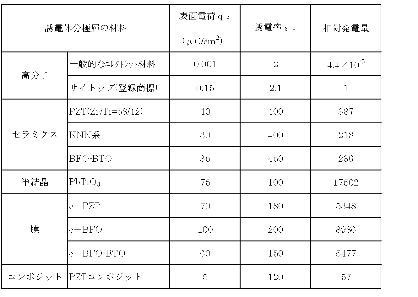
As shown in Table 1, when Cytop or an inorganic substance is used, a power generation amount that is significantly larger than a general electret material amount can be obtained. In addition, even for non-oriented inorganic materials, the amount of power generation is estimated several hundred times that of Cytop, and further, the amount of power generation is estimated to be several thousand times that of membranes and 16,000 times that of single crystals. It was. Further, a PZT composite in which PZT is dispersed in a polymer material can also generate a power generation amount several tens of times that of Cytop.
「設計変更」
本発明は上記実施の形態に限定されるものではなく、発明の要旨を変更しない限りにおいて、種々変更することが可能である。 "Design changes"
The present invention is not limited to the above embodiment, and various modifications can be made without changing the gist of the invention.
本発明は上記実施の形態に限定されるものではなく、発明の要旨を変更しない限りにおいて、種々変更することが可能である。 "Design changes"
The present invention is not limited to the above embodiment, and various modifications can be made without changing the gist of the invention.
例えば、上述の電極、誘電分極体および誘電エラストマーを複数積層し、それらを直列または並列接続して発電量を向上させた発電装置を構成してもよい。
For example, a power generation apparatus in which a plurality of the above-described electrodes, dielectric polarization bodies, and dielectric elastomers are stacked and connected in series or in parallel may improve the power generation amount.
本発明の発電素子は、波力、水力、風力などの自然エネルギーによる発電をはじめ、靴や床に埋め込まれ人の歩行による発電、自動車のタイヤ等に埋め込まれ自動車の走行による発電などに利用可能である。
The power generation element of the present invention can be used for power generation by natural energy such as wave power, hydraulic power, wind power, etc., power generation by walking of people embedded in shoes and floors, power generation by running of automobiles embedded in automobile tires, etc. It is.
Claims (7)
- 静電容量変化型の発電素子であって、
誘電分極体と誘電エラストマー層とが積層されてなる積層体、および
該積層体の積層方向の上下に配された一対の電極を備え、
前記誘電分極体が結晶配向性を有する強誘電体からなることを特徴とする発電素子。 A capacitance change type power generation element,
A laminated body in which a dielectric polarization body and a dielectric elastomer layer are laminated, and a pair of electrodes arranged above and below in the laminating direction of the laminated body,
The power generation element, wherein the dielectric polarization body is made of a ferroelectric having crystal orientation. - 前記強誘電体の比誘電率が最小となる分極軸が、層厚方向に略平行に配向していることを特徴とする請求項1記載の発電素子。 2. The power generating element according to claim 1, wherein a polarization axis at which a relative dielectric constant of the ferroelectric is minimum is oriented substantially parallel to the layer thickness direction.
- 前記誘電分極体の残留分極値が5μC/cm2以上であり、比誘電率が400以下であることを特徴とする請求項1または2記載の発電素子。 3. The power generating element according to claim 1, wherein a remanent polarization value of the dielectric polarization body is 5 μC / cm 2 or more and a relative dielectric constant is 400 or less.
- 前記強誘電体が、単結晶であることを特徴とする請求項1から3いずれか1項記載の発電素子。 The power generation element according to any one of claims 1 to 3, wherein the ferroelectric is a single crystal.
- 前記誘電エラストマー層のヤング率が100MPa以下であることを特徴とする請求項1から4いずれか1項記載の発電素子。 The power generation element according to any one of claims 1 to 4, wherein the dielectric elastomer layer has a Young's modulus of 100 MPa or less.
- 前記強誘電体の結晶構造がペロブスカイト構造、ビスマス層状構造、タングステンブロンズ構造のいずれかであることを特徴とする請求項1から5いずれか1項記載の発電素子。 The power generation element according to any one of claims 1 to 5, wherein a crystal structure of the ferroelectric material is any one of a perovskite structure, a bismuth layer structure, and a tungsten bronze structure.
- 前記強誘電体が、鉛を含まないペロブスカイト型酸化物を主成分とすることを特徴とする請求項1から6いずれか1項記載の発電素子。 The power generation element according to any one of claims 1 to 6, wherein the ferroelectric material contains a perovskite oxide containing no lead as a main component.
Applications Claiming Priority (2)
| Application Number | Priority Date | Filing Date | Title |
|---|---|---|---|
| JP2011-022342 | 2011-02-04 | ||
| JP2011022342A JP2012164727A (en) | 2011-02-04 | 2011-02-04 | Electrostatic capacity variation type power generation element |
Publications (1)
| Publication Number | Publication Date |
|---|---|
| WO2012105187A1 true WO2012105187A1 (en) | 2012-08-09 |
Family
ID=46602414
Family Applications (1)
| Application Number | Title | Priority Date | Filing Date |
|---|---|---|---|
| PCT/JP2012/000455 WO2012105187A1 (en) | 2011-02-04 | 2012-01-25 | Capacitance-varying type power-generation element |
Country Status (2)
| Country | Link |
|---|---|
| JP (1) | JP2012164727A (en) |
| WO (1) | WO2012105187A1 (en) |
Cited By (2)
| Publication number | Priority date | Publication date | Assignee | Title |
|---|---|---|---|---|
| JP2014179549A (en) * | 2013-03-15 | 2014-09-25 | Ricoh Co Ltd | Method for manufacturing electromechanical conversion element, electromechanical conversion element, droplet discharge head, droplet discharge device and device for manufacturing electromechanical conversion element |
| TWI827012B (en) * | 2022-02-02 | 2023-12-21 | 台灣積體電路製造股份有限公司 | Integrated chip and method of forming the same |
Families Citing this family (4)
| Publication number | Priority date | Publication date | Assignee | Title |
|---|---|---|---|---|
| JP6633852B2 (en) * | 2014-07-28 | 2020-01-22 | ローム株式会社 | Piezoelectric element and inkjet head |
| JP6870200B2 (en) | 2014-11-13 | 2021-05-12 | 株式会社リコー | Elements and power generators |
| JP6699119B2 (en) | 2015-01-22 | 2020-05-27 | 株式会社リコー | Element and power generator |
| JP6618035B2 (en) | 2015-03-09 | 2019-12-11 | 株式会社リコー | Element and power generation device |
Citations (4)
| Publication number | Priority date | Publication date | Assignee | Title |
|---|---|---|---|---|
| JP2003146660A (en) * | 2001-11-13 | 2003-05-21 | Fuji Electric Co Ltd | Ferroelectric substance, ferroelectric thin film capacitor, and piezoelectric element |
| JP2006131776A (en) * | 2004-11-08 | 2006-05-25 | Saitama Univ | Composite member having self-diagnostic function and its production process |
| JP2008053527A (en) * | 2006-08-25 | 2008-03-06 | Nsk Ltd | Dielectric rubber laminate, and its manufacturing method |
| JP2009224740A (en) * | 2008-03-19 | 2009-10-01 | Fujifilm Corp | Laminated structure and device using the same, method of manufacturing device, and liquid ejection device |
-
2011
- 2011-02-04 JP JP2011022342A patent/JP2012164727A/en not_active Withdrawn
-
2012
- 2012-01-25 WO PCT/JP2012/000455 patent/WO2012105187A1/en active Application Filing
Patent Citations (4)
| Publication number | Priority date | Publication date | Assignee | Title |
|---|---|---|---|---|
| JP2003146660A (en) * | 2001-11-13 | 2003-05-21 | Fuji Electric Co Ltd | Ferroelectric substance, ferroelectric thin film capacitor, and piezoelectric element |
| JP2006131776A (en) * | 2004-11-08 | 2006-05-25 | Saitama Univ | Composite member having self-diagnostic function and its production process |
| JP2008053527A (en) * | 2006-08-25 | 2008-03-06 | Nsk Ltd | Dielectric rubber laminate, and its manufacturing method |
| JP2009224740A (en) * | 2008-03-19 | 2009-10-01 | Fujifilm Corp | Laminated structure and device using the same, method of manufacturing device, and liquid ejection device |
Cited By (2)
| Publication number | Priority date | Publication date | Assignee | Title |
|---|---|---|---|---|
| JP2014179549A (en) * | 2013-03-15 | 2014-09-25 | Ricoh Co Ltd | Method for manufacturing electromechanical conversion element, electromechanical conversion element, droplet discharge head, droplet discharge device and device for manufacturing electromechanical conversion element |
| TWI827012B (en) * | 2022-02-02 | 2023-12-21 | 台灣積體電路製造股份有限公司 | Integrated chip and method of forming the same |
Also Published As
| Publication number | Publication date |
|---|---|
| JP2012164727A (en) | 2012-08-30 |
Similar Documents
| Publication | Publication Date | Title |
|---|---|---|
| WO2012105187A1 (en) | Capacitance-varying type power-generation element | |
| WO2012108192A1 (en) | Capacitance change type electric power generating element | |
| KR102293796B1 (en) | Triboelectric generating device | |
| JP5076026B2 (en) | Capacitance element and resonance circuit | |
| JP5702125B2 (en) | Electrostatic induction type conversion element | |
| KR101417855B1 (en) | Cantilever type energy harverster | |
| TW201027815A (en) | Piezoelectric element | |
| CN104882277A (en) | Adjustable and controllable capacitor with layered composite structure, and method of adjusting and controlling dielectric through piezoelectric stress | |
| JP6402652B2 (en) | Dielectric composition and electronic component | |
| CN105185899A (en) | Preparation method of piezoelectric ceramic polymer composite material | |
| WO2021256370A1 (en) | Drive method, drive circuit, and displacement drive device | |
| US9147828B2 (en) | Piezoelectric drive element and piezoelectric drive unit | |
| TW201830743A (en) | Actuator | |
| JP2009170631A (en) | Piezoelectric element and method of manufacturing the same, and piezoelectric application device using the same | |
| Kim et al. | Low-temperature co-fired multilayer cantilevers based on relaxor–Pb (Zr, Ti) O3 for enhanced piezoelectric power generation at nonresonant frequency | |
| KR101188331B1 (en) | Piezoelectric Element | |
| Shin et al. | A comparative research on maximized output power between disc type and multilayered type piezoelectric energy harvesters | |
| JPS61283180A (en) | Laminated piezoelectric substance | |
| US9153768B2 (en) | Piezoelectric/electrostrictive ceramics composition and displacement generating device | |
| Kumar et al. | Nanocrystalline PNS-PZT-Based Energy Harvester for Strategic Applications | |
| Vucheva et al. | Comparison of the piezoelectric properties of single-layer and bilayer structures with thin films of PZT and ZnO in dynamic mode | |
| Kim et al. | Piezoelectric Materials-based Nanogenerators | |
| Subramani et al. | Advances in Polymer-Based Piezoelectric Systems | |
| Alghamdi | Energy Harvesting of Lead-free Piezoelectric Ceramics Bimorphs | |
| KR20160007029A (en) | Piezoelectric element and piezoelectric vibration module including the same |
Legal Events
| Date | Code | Title | Description |
|---|---|---|---|
| 121 | Ep: the epo has been informed by wipo that ep was designated in this application |
Ref document number: 12741680 Country of ref document: EP Kind code of ref document: A1 |
|
| NENP | Non-entry into the national phase |
Ref country code: DE |
|
| 122 | Ep: pct application non-entry in european phase |
Ref document number: 12741680 Country of ref document: EP Kind code of ref document: A1 |