WO2012096197A2 - A power supply device, inverter device, and power tool - Google Patents
A power supply device, inverter device, and power tool Download PDFInfo
- Publication number
- WO2012096197A2 WO2012096197A2 PCT/JP2012/000208 JP2012000208W WO2012096197A2 WO 2012096197 A2 WO2012096197 A2 WO 2012096197A2 JP 2012000208 W JP2012000208 W JP 2012000208W WO 2012096197 A2 WO2012096197 A2 WO 2012096197A2
- Authority
- WO
- WIPO (PCT)
- Prior art keywords
- voltage
- control unit
- inverter
- battery pack
- output
- Prior art date
Links
Images

Classifications
-
- H—ELECTRICITY
- H02—GENERATION; CONVERSION OR DISTRIBUTION OF ELECTRIC POWER
- H02J—CIRCUIT ARRANGEMENTS OR SYSTEMS FOR SUPPLYING OR DISTRIBUTING ELECTRIC POWER; SYSTEMS FOR STORING ELECTRIC ENERGY
- H02J7/00—Circuit arrangements for charging or depolarising batteries or for supplying loads from batteries
- H02J7/0063—Circuit arrangements for charging or depolarising batteries or for supplying loads from batteries with circuits adapted for supplying loads from the battery
-
- H—ELECTRICITY
- H02—GENERATION; CONVERSION OR DISTRIBUTION OF ELECTRIC POWER
- H02J—CIRCUIT ARRANGEMENTS OR SYSTEMS FOR SUPPLYING OR DISTRIBUTING ELECTRIC POWER; SYSTEMS FOR STORING ELECTRIC ENERGY
- H02J7/00—Circuit arrangements for charging or depolarising batteries or for supplying loads from batteries
- H02J7/007—Regulation of charging or discharging current or voltage
- H02J7/00712—Regulation of charging or discharging current or voltage the cycle being controlled or terminated in response to electric parameters
- H02J7/007182—Regulation of charging or discharging current or voltage the cycle being controlled or terminated in response to electric parameters in response to battery voltage
-
- H—ELECTRICITY
- H02—GENERATION; CONVERSION OR DISTRIBUTION OF ELECTRIC POWER
- H02J—CIRCUIT ARRANGEMENTS OR SYSTEMS FOR SUPPLYING OR DISTRIBUTING ELECTRIC POWER; SYSTEMS FOR STORING ELECTRIC ENERGY
- H02J2207/00—Indexing scheme relating to details of circuit arrangements for charging or depolarising batteries or for supplying loads from batteries
- H02J2207/20—Charging or discharging characterised by the power electronics converter
-
- H—ELECTRICITY
- H02—GENERATION; CONVERSION OR DISTRIBUTION OF ELECTRIC POWER
- H02J—CIRCUIT ARRANGEMENTS OR SYSTEMS FOR SUPPLYING OR DISTRIBUTING ELECTRIC POWER; SYSTEMS FOR STORING ELECTRIC ENERGY
- H02J7/00—Circuit arrangements for charging or depolarising batteries or for supplying loads from batteries
- H02J7/0029—Circuit arrangements for charging or depolarising batteries or for supplying loads from batteries with safety or protection devices or circuits
- H02J7/00306—Overdischarge protection
-
- H—ELECTRICITY
- H02—GENERATION; CONVERSION OR DISTRIBUTION OF ELECTRIC POWER
- H02M—APPARATUS FOR CONVERSION BETWEEN AC AND AC, BETWEEN AC AND DC, OR BETWEEN DC AND DC, AND FOR USE WITH MAINS OR SIMILAR POWER SUPPLY SYSTEMS; CONVERSION OF DC OR AC INPUT POWER INTO SURGE OUTPUT POWER; CONTROL OR REGULATION THEREOF
- H02M1/00—Details of apparatus for conversion
- H02M1/0067—Converter structures employing plural converter units, other than for parallel operation of the units on a single load
- H02M1/007—Plural converter units in cascade
Definitions
- the present invention relates to a power supply device, an inverter device and a power tool provided with the power supply device or the inverter device.
- An electronic device provided with an inverter circuit boosts AC voltage supplied from a commercial power source, rectifies/smooths the boosted AC voltage into DC voltage, converts the DC voltage into predetermined AC voltage using the inverter circuit, and outputs the predetermined AC voltage to an AC motor provided in the electronic device.
- Japanese Patent Application Publication No. 2009-278832 provides a technique that operates the AC motor provided in the electronic device with DC voltage supplied from a battery pack instead of the AC voltage supplied from the commercial power source.
- an inverter device provided with a converting circuit, a booster circuit, a rectifying/smoothing circuit, and an inverter circuit are connected between the battery pack and the electronic device to supply AC power to the electronic device.
- the electronic device is configured to operate with voltage within a suitable range.
- the voltage supplied to the electronic device may decrease due to a decrease in the battery voltage during use or a decrease in voltage during an overload condition. Consequently, there is a possibility that the electronic device connected to the inverter device may malfunction as a result of a voltage outside the suitable range being supplied thereto.
- the invention provides a power supply device including: a battery pack; a transforming unit configured to transform a DC voltage supplied from the battery pack; and a control unit configured to prevent the transforming unit from performing an operation when a voltage outputted from the transforming unit is outside a prescribed range.
- the transforming unit includes: a converting unit configured to convert the DC voltage supplied from the battery pack into an AC voltage; and a rectifying/smoothing circuit configured to rectifies/smooths the AC voltage.
- the control unit prevents the transforming unit from performing an operation when a voltage outputted from the rectifying/smoothing circuit is outside a prescribed range.
- the inverter circuit further includes an inverter circuit configured to convert the voltage outputted from the rectifying/smoothing circuit into an AC voltage.
- the control unit prevents the inverter circuit from performing an operation when the voltage outputted from the rectifying/smoothing circuit is outside the prescribed range.
- control unit allows the transforming unit to perform the operation during a given period when the voltage outputted from the transforming unit falls below a lower limit.
- control unit prevents the transforming unit from performing the operation immediately after the voltage outputted from the transforming unit exceeds an upper limit.
- an inverter device including: a converting unit configured to convert a first DC voltage into a first AC voltage and output the first AC voltage; a rectifying/smoothing circuit configured to convert the first AC voltage into a second DC voltage and output the second DC voltage; an inverter circuit configured to convert the second DC voltage into a second AC voltage and output the second AC voltage; and a control unit configured to prevent the inverter circuit from outputting the second AC voltage at least one of when the second DC voltage exceeds an upper limit and when the second DC voltage falls below a lower limit.
- control unit prevents the inverter circuit from outputting the second AC voltage when the second DC voltage is outside a prescribed range.
- control unit prevents the inverter circuit from outputting the second AC voltage when the second DC voltage remains outside the prescribed range during a given period.
- control unit prevents the converting unit from outputting the first AC voltage when the second DC voltage is outside a prescribed range.
- control unit prevents the converting unit from outputting the first AC voltage when the second DC voltage remains outside the prescribed range during a given period.
- Another aspect of the invention provides a power tool including an AC motor connectable to the power supply device.
- Another aspect of the invention provides a power tool including an AC motor connectable to the inverter device.
- the power supply device of the present invention can prevent a voltage outside a suitable range from being supplied to an electronic device.
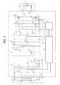
- Fig. 1 is a circuit diagram for an inverter device according to a preferred embodiment of the present invention.
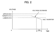
- Fig. 2 is a timing chart illustrating a process to halt output from the inverter device according to the preferred embodiment.
- Fig. 3 is a flowchart illustrating steps in a process for halting output from the inverter device according to the preferred embodiment.
- Fig. 1 is a circuit diagram for the inverter device 1.
- the inverter device 1 is connected between a battery pack 2 and an electronic device 3 to convert a DC power supplied from the battery pack 2 into an AC power and outputs the AC power to an AC motor 31 provided in the electronic device 3.
- the inverter device 1 converts DC power supplied from the battery pack 2 to AC power and supplies this AC power to the AC motor 31 of the electronic device 3.
- the inverter device 1, electronic device 3, and battery pack 2 are detachably connected to one another, the following description assumes that these components are connected.
- the electronic device 3 includes a power tool driven with 100V of AC voltage, such as a lawn.
- the inverter device 1 includes a battery voltage detection unit 11, a power supply unit 12, a booster circuit 13, a rectifying/smoothing circuit 14, a boost voltage detection unit 15, an inverter circuit 16, a current detection resistor 17, a PWM signal output unit 18, and a control unit 19.
- the battery voltage detection unit 11 includes battery voltage detection resistors 111 and 112.
- the battery voltage detection resistors 111 and 112 are connected in series between a plus terminal 21 and a minus terminal 22 of the battery pack 2 to output a divided voltage of the battery voltage of the battery pack 2 by the battery voltage detection resistors 111 and 112 to the control unit 19.
- the battery pack 2 shown in Fig. 1 has four 3.6-V lithium battery cells 2a connected in series for outputting a rated voltage of 14.4 V.
- the power supply unit 12 includes a power switch 121 and a constant-voltage circuit 122 connected in series between the plus terminal 21 of the battery pack 2 and the control unit 19.
- the constant-voltage circuit 122 includes a three-terminal regulator 122a, and oscillation-prevention capacitors 122b and 122c.
- the constant-voltage circuit 122 converts the voltage supplied from the battery pack 2 into a prescribed DC voltage (5 V, for example) and supplies this voltage to the control unit 19 as drive voltage.
- the entire inverter device 1 is turned off because the drive voltage is no longer supplied to the control unit 19.
- the booster circuit 13 is configured of a transformer 131, and a field effect transistor (FET) 132 that serves as the converting unit.
- the transformer 131 includes a primary winding 131a, and a secondary winding 131b.
- the primary winding 131a is connected between the plus terminal 21 and minus terminal 22 of the battery pack 2.
- the FET 132 is provided between the primary winding 131a of the transformer 131 and the minus terminal 22 of the battery pack 2.
- the control unit 19 inputs a first PWM signal into the gate of the FET 132 for switching the FET 132 on and off. Through on/off switching of the FET 132, the DC power supplied from the battery pack 2 to the primary winding 131a of the transformer 131 is converted into AC power.
- the AC voltage of this AC power is stepped up based on the ratio of the number of turns in the secondary winding 131b to the number of turns in the primary winding 131a, and is outputted from the secondary winding 131b.
- the rectifying/smoothing circuit 14 is configured of rectifying diodes 141 and 142, and a smoothing capacitor 143. Through this configuration, the rectifying/smoothing circuit 14 converts the AC voltage stepped up by the transformer 131 to DC voltage (141 V, for example).
- the boost voltage detection unit 15 includes resistors 151 and 152 connected in series to output a divided voltage of the DC voltage outputted from the rectifying/smoothing circuit 14 (the voltage at the smoothing capacitor 143; 141 V, for example) by the resistors 151 and 152 to the control unit 19.
- the inverter circuit 16 is configured of four FETs 161-164.
- the FETs 161 and 162 are connected in series, and the FETs 163 and 164, with both pairs of FETs being connected to the smoothing capacitor 143 in parallel. More specifically, the drain of the FET 161 is connected to the cathodes of the rectifying diodes 141 and 142, while the source of the FET 161 is connected to the drain of the FET 162. Similarly, the drain of the FET 163 is connected to the cathodes of the rectifying diodes 141 and 142, while the source of the FET 163 is connected to the drain of the FET 164.
- the inverter circuit 16 also includes output terminals 165 and 166 that are connected to the AC motor 31 of the electronic device 3.
- the source of the FET 161 and the drain of the FET 162 are connected to the output terminal 165, while the source of the FET 163 and the drain of the FET 164 are connected to the output terminal 166.
- the PWM signal output unit 18 outputs second PWM signals to the gates of the FETs 161-164 for switching the FETs 161-164 on and off. Through on/off switching of the FETs 161-164, the inverter circuit 16 converts the DC power outputted from the rectifying/smoothing circuit 14 into AC power and supplies this AC power to the electronic device 3 (the AC motor 31).
- the current detection resistor 17 is connected between the source of the FET 162 (FET 164) and the minus terminal 22 of the battery pack 2.
- the terminal of the current detection resistor 17 on the high-voltage side is also connected to the control unit 19. With this configuration, the control unit 19 can determine the current flowing to the AC motor 31 based on the voltage detected by the current detection resistor 17.
- the control unit 19 outputs the first PWM signal to the gate of the FET 132 based on the boosted voltage detected by the boost voltage detection unit 15 in order that the AC voltage outputted from the secondary side of the transformer 131 has the desired effective voltage (141 V, for example).
- the control unit 19 also outputs the second PWM signals to the gates of the FETs 161-164 via the PWM signal output unit 18 in order that the AC voltage outputted to the AC motor 31 has the desired effective voltage (100 V, for example).
- the FETs 161 and 164 are treated as one set (hereinafter referred to as the "first set"), while the FETs 162 and 163 are treated as another set (hereinafter referred to as the "second set"), and the control unit 19 outputs the second PWM signals for alternately turning on and off the first and second sets at a duty cycle of 100%.
- the control unit 19 also determines whether over-discharge has occurred in the battery pack 2 based on the battery voltage detected by the battery voltage detection unit 11. More specifically, when the battery voltage detected by the battery voltage detection unit 11 is smaller than a prescribed over-discharge voltage, the control unit 19 determines that over-discharge has occurred in the battery pack 2 and outputs the first and second PWM signals in order to halt output to the AC motor 31. That is, the control unit 19 halts output of the first and second PWM signals.
- the battery pack 2 is further provided with a built-in protection circuit or microcomputer and possesses a function for self-detecting over-discharge and for outputting an over-discharge signal to the control unit 19.
- the control unit 19 receives an over-discharge signal from the battery pack 2 via a signal terminal LD, the control unit 19 outputs first and second PWM signals in order to halt output to the AC motor 31. That is, the control unit 19 halts output of the first and second PWM signals.
- This construction can prevent such over-discharge from shortening the lifespan of the battery pack 2.
- the electronic device 3 is configured to operate with voltage within a suitable range.
- the voltage supplied to the electronic device 3 may decrease due to a decrease in the battery voltage during use or a decrease in voltage during an overload condition. Consequently, there is a possibility that the electronic device 3 connected to the inverter device 1 may malfunction as a result of a voltage outside the suitable range being supplied thereto.
- the control unit 19 outputs first and second PWM signals for halting output to the AC motor 31 when the voltage boosted by the booster circuit 13 (the voltage at the smoothing capacitor 143 detected by the boost voltage detection unit 15) is outside a prescribed range defined by an upper limit (155 V in the preferred embodiment) and a lower limit (127 V), as illustrated in the timing chart of Fig. 2. Specifically, the control unit 19 halts output of the first and second PWM signals in this case.
- the control process performed by the control unit 19 for halting output to the AC motor 31 will be described with reference to the flowchart in Fig. 3.
- the control unit 19 begins the process in Fig. 3 either when the power switch 121 is turned on while the battery pack 2 is mounted on the inverter device 1 or when the battery pack 2 is mounted on the inverter device 1 while the power switch 121 is in an ON state.
- the constant-voltage circuit 122 When the power switch 121 is turned on, the constant-voltage circuit 122 generates a drive voltage for driving the control unit 19 from the battery voltage of the battery pack 2.
- control unit 19 In S101 of the flowchart in Fig. 3, the control unit 19 outputs the first PWM signal to the gate of the FET 132 in order that the AC voltage outputted from the secondary side of the transformer 131 has the desired effective voltage (100 V, for example). In S102 the control unit 19 determines whether the effective voltage boosted by the transformer 131 is greater than the target voltage based on the voltage detected by the boost voltage detection unit 15.
- the control unit 19 reduces the duty cycle of the FET 132.
- the control unit 19 increases the duty cycle of the FET 132.
- the control unit 19 determines whether the battery voltage of the battery pack 2 is less than a prescribed over-discharge voltage based on the voltage detected by the battery voltage detection unit 11. If the battery voltage is less than the prescribed over-discharge voltage (S105: YES), then the control unit 19 determines that the battery pack 2 is in an over-discharge state. Accordingly, in S111 the control unit 19 outputs first and second PWM signals for halting output to the AC motor 31. Specifically, the control unit 19 halts output of the first and second PWM signals. As a result, operations of the booster circuit 13 and inverter circuit 16 are shut down, thereby halting output from the inverter device 1 to the AC motor 31.
- the control unit 19 determines whether an over-discharge signal was inputted from the battery pack 2 via the LD terminal. If an over-discharge signal was inputted (S106: YES), then the control unit 19 determines that the battery pack 2 is in an over-discharge state. Accordingly, in S111 the control unit 19 outputs the first and second PWM signals for halting output to the AC motor 31. Specifically, the control unit 19 halts output of the first and second PWM signals.
- control unit 19 determines whether the boosted voltage is greater than a prescribed upper limit (155 V in the preferred embodiment). If the boosted voltage is greater than the upper limit (S107: YES), in S108 the control unit 19 determines whether the state in which the boosted voltage is greater than the prescribed upper limit has continued for more than 0.5 seconds. If the high boosted voltage has continued for this time (S108: YES), in S111 the control unit 19 outputs the first and second PWM signals for halting output to the AC motor 31.
- a prescribed upper limit 155 V in the preferred embodiment.
- the inverter device 1 can prevent damage to the power tool.
- the inverter device 1 can simultaneously prevent damage to components in the inverter device 1, such as the FETs in the inverter circuit 16. Although it is rare during normal operations for the boosted voltage to rise above the prescribed upper limit, this type of control process effectively protects the inverter device 1 should the control unit 19 or boost voltage detection unit 15 responsible for controlling the boosted voltage become damaged.
- the voltage will rise or fall temporarily due to noise and the like. Halting output to the AC motor 31 even in these cases could cause the electronic device 3 to malfunction. Therefore, output to the AC motor 31 is only halted in the preferred embodiment when the boosted voltage remains higher than the prescribed upper limit continuously for at least 0.5 seconds.
- the control unit 19 determines whether the boosted voltage is less than a prescribed lower limit (127 V in the preferred embodiment). If the boosted voltage is smaller than the lower limit (S109: YES), in S110 the control unit 19 determines whether the boosted voltage has been in a state lower than the prescribed lower limit for a continuous 3.0 seconds or greater. If the boosted voltage has been in this state continuously for the prescribed time (S110: YES), in S111 the control unit 19 outputs the first and second PWM signals for halting output to the AC motor 31.
- a prescribed lower limit 127 V in the preferred embodiment. If the boosted voltage is smaller than the lower limit (S109: YES), in S110 the control unit 19 determines whether the boosted voltage has been in a state lower than the prescribed lower limit for a continuous 3.0 seconds or greater. If the boosted voltage has been in this state continuously for the prescribed time (S110: YES), in S111 the control unit 19 outputs the first and second PWM signals for halting output to the AC motor 31.
- the inverter device 1 halts output to the AC motor 31 when the voltage boosted by the booster circuit 13 (the voltage detected by the boost voltage detection unit 15) falls outside the prescribed range defined by an upper limit (155 V) and a lower limit (127 V). Hence, the inverter device 1 can prevent a malfunction of the electronic equipment caused when a voltage outside the suitable range is supplied thereto.
- the inverter device 1 halts output to the AC motor 31 only when the detected voltage has remained continuously outside the prescribed range for a prescribed time or greater.
- the inverter device 1 can prevent output to the AC motor 31 from being halted when the voltage rises or drops temporarily due to noise and the like.
- the inverter device 1 may be configured to output only one of the PWM signals for halting output to the AC motor 31, while the inverter device 1 is configured to output the first and second PWM signals for halting output to the AC motor 31 in the preferred embodiment described above.
- the inverter device 1 can halt output to the AC motor 31 by halting output of one of the first PWM signal and the second PWM signals.
- halting output of both first and second PWM signals can suppress power consumption in the battery pack 2.
- 155 V and 127 V are used respectively as the upper and lower limits of the prescribed range, but the prescribed range is not limited to these boundaries.
- the battery pack 2 that is connected to the inverter device 1 in the preferred embodiment described above is a 14.4 V lithium battery pack, but the inverter device 1 may be configured to be connectable to different types of battery packs in addition to those housing lithium batteries, such as battery packs configured of nickel cadmium batteries or nickel metal hydride batteries, or may be configured to be connectable to a plurality of battery packs with various battery voltages.
- steps for controlling the boosted voltage in S101-S104, for detecting over-discharge in S105-S106, and for controlling the halting of output in S107-S110 of Fig. 3 may be performed at any position in the flowchart or may be performed in parallel.
- the inverter device 1 may also store a count value indicating the number of times that output to the AC motor 31 was halted due to the voltage boosted by the booster circuit 13 being outside the prescribed range, and may display this history of halted output.
- the inverter device 1 may be configured to notify the user that the battery pack 2 has reached the end of its service life when output to the AC motor 31 has been halted more than a prescribed number of times.
- an overcurrent detection may be further performed. Specifically, the control unit 19 halts the operations of the booster circuit unit 13 and inverter circuit 16 when the current detected by the current detection resistor 17 has exceeded a predetermined current. With this construction, it can prevented that the battery pack 2, the AC motor 32, and FETs 132 and 161-164 are damaged due to the heat generated by the overcurrent.
Abstract
A power supply device includes: a battery pack; a transforming unit configured to transform a DC voltage supplied from the battery pack; and a control unit configured to prevent the transforming unit from performing an operation when a voltage outputted from the transforming unit is outside a prescribed range.
Description
The present invention relates to a power supply device, an inverter device and a power tool provided with the power supply device or the inverter device.
An electronic device provided with an inverter circuit is well-known. Such the electronic device boosts AC voltage supplied from a commercial power source, rectifies/smooths the boosted AC voltage into DC voltage, converts the DC voltage into predetermined AC voltage using the inverter circuit, and outputs the predetermined AC voltage to an AC motor provided in the electronic device.
Japanese Patent Application Publication No. 2009-278832 provides a technique that operates the AC motor provided in the electronic device with DC voltage supplied from a battery pack instead of the AC voltage supplied from the commercial power source.
In the above technique, an inverter device provided with a converting circuit, a booster circuit, a rectifying/smoothing circuit, and an inverter circuit are connected between the battery pack and the electronic device to supply AC power to the electronic device.
Normally, the electronic device is configured to operate with voltage within a suitable range. However, the voltage supplied to the electronic device may decrease due to a decrease in the battery voltage during use or a decrease in voltage during an overload condition. Consequently, there is a possibility that the electronic device connected to the inverter device may malfunction as a result of a voltage outside the suitable range being supplied thereto.
In view of the foregoing, it is an object of the present invention to provide a power supply device capable of preventing a voltage outside a suitable range from being supplied to an electronic device.
In order to attain the above and other objects, the invention provides a power supply device including: a battery pack; a transforming unit configured to transform a DC voltage supplied from the battery pack; and a control unit configured to prevent the transforming unit from performing an operation when a voltage outputted from the transforming unit is outside a prescribed range.
It is preferable that the transforming unit includes: a converting unit configured to convert the DC voltage supplied from the battery pack into an AC voltage; and a rectifying/smoothing circuit configured to rectifies/smooths the AC voltage. The control unit prevents the transforming unit from performing an operation when a voltage outputted from the rectifying/smoothing circuit is outside a prescribed range.
It is preferable that the inverter circuit further includes an inverter circuit configured to convert the voltage outputted from the rectifying/smoothing circuit into an AC voltage. The control unit prevents the inverter circuit from performing an operation when the voltage outputted from the rectifying/smoothing circuit is outside the prescribed range.
It is preferable that the control unit allows the transforming unit to perform the operation during a given period when the voltage outputted from the transforming unit falls below a lower limit.
It is preferable that the control unit prevents the transforming unit from performing the operation immediately after the voltage outputted from the transforming unit exceeds an upper limit.
Another aspect of the present invention provides an inverter device including: a converting unit configured to convert a first DC voltage into a first AC voltage and output the first AC voltage; a rectifying/smoothing circuit configured to convert the first AC voltage into a second DC voltage and output the second DC voltage; an inverter circuit configured to convert the second DC voltage into a second AC voltage and output the second AC voltage; and a control unit configured to prevent the inverter circuit from outputting the second AC voltage at least one of when the second DC voltage exceeds an upper limit and when the second DC voltage falls below a lower limit.
It is preferable that the control unit prevents the inverter circuit from outputting the second AC voltage when the second DC voltage is outside a prescribed range.
It is preferable that the control unit prevents the inverter circuit from outputting the second AC voltage when the second DC voltage remains outside the prescribed range during a given period.
It is preferable that the control unit prevents the converting unit from outputting the first AC voltage when the second DC voltage is outside a prescribed range.
It is preferable that the control unit prevents the converting unit from outputting the first AC voltage when the second DC voltage remains outside the prescribed range during a given period.
Another aspect of the invention provides a power tool including an AC motor connectable to the power supply device.
Another aspect of the invention provides a power tool including an AC motor connectable to the inverter device.
The power supply device of the present invention can prevent a voltage outside a suitable range from being supplied to an electronic device.
1 Inverter device
13 Booster circuit
132 FET
14 Rectifying/smoothing circuit
16 Inverter circuit
19 Control unit
2 Battery pack
3 Electronic device
13 Booster circuit
132 FET
14 Rectifying/smoothing circuit
16 Inverter circuit
19 Control unit
2 Battery pack
3 Electronic device
An inverter device 1 according to a preferred embodiment of the power supply device of the present invention will be described while referring to Figs. 1 through 3.
Fig. 1 is a circuit diagram for the inverter device 1. The inverter device 1 is connected between a battery pack 2 and an electronic device 3 to convert a DC power supplied from the battery pack 2 into an AC power and outputs the AC power to an AC motor 31 provided in the electronic device 3. When an operator operates a trigger switch 32 provided in the electronic device 3, the inverter device 1 converts DC power supplied from the battery pack 2 to AC power and supplies this AC power to the AC motor 31 of the electronic device 3. While the inverter device 1, electronic device 3, and battery pack 2 are detachably connected to one another, the following description assumes that these components are connected. The electronic device 3 includes a power tool driven with 100V of AC voltage, such as a lawn.
The inverter device 1 includes a battery voltage detection unit 11, a power supply unit 12, a booster circuit 13, a rectifying/smoothing circuit 14, a boost voltage detection unit 15, an inverter circuit 16, a current detection resistor 17, a PWM signal output unit 18, and a control unit 19.
The battery voltage detection unit 11 includes battery voltage detection resistors 111 and 112. The battery voltage detection resistors 111 and 112 are connected in series between a plus terminal 21 and a minus terminal 22 of the battery pack 2 to output a divided voltage of the battery voltage of the battery pack 2 by the battery voltage detection resistors 111 and 112 to the control unit 19. The battery pack 2 shown in Fig. 1 has four 3.6-V lithium battery cells 2a connected in series for outputting a rated voltage of 14.4 V.
The power supply unit 12 includes a power switch 121 and a constant-voltage circuit 122 connected in series between the plus terminal 21 of the battery pack 2 and the control unit 19. The constant-voltage circuit 122 includes a three-terminal regulator 122a, and oscillation- prevention capacitors 122b and 122c. When an operator turns on the power switch 121, the constant-voltage circuit 122 converts the voltage supplied from the battery pack 2 into a prescribed DC voltage (5 V, for example) and supplies this voltage to the control unit 19 as drive voltage. When the operator switches off the power switch 121, the entire inverter device 1 is turned off because the drive voltage is no longer supplied to the control unit 19.
The booster circuit 13 is configured of a transformer 131, and a field effect transistor (FET) 132 that serves as the converting unit. The transformer 131 includes a primary winding 131a, and a secondary winding 131b. The primary winding 131a is connected between the plus terminal 21 and minus terminal 22 of the battery pack 2. The FET 132 is provided between the primary winding 131a of the transformer 131 and the minus terminal 22 of the battery pack 2. The control unit 19 inputs a first PWM signal into the gate of the FET 132 for switching the FET 132 on and off. Through on/off switching of the FET 132, the DC power supplied from the battery pack 2 to the primary winding 131a of the transformer 131 is converted into AC power. The AC voltage of this AC power is stepped up based on the ratio of the number of turns in the secondary winding 131b to the number of turns in the primary winding 131a, and is outputted from the secondary winding 131b.
The rectifying/smoothing circuit 14 is configured of rectifying diodes 141 and 142, and a smoothing capacitor 143. Through this configuration, the rectifying/smoothing circuit 14 converts the AC voltage stepped up by the transformer 131 to DC voltage (141 V, for example).
The boost voltage detection unit 15 includes resistors 151 and 152 connected in series to output a divided voltage of the DC voltage outputted from the rectifying/smoothing circuit 14 (the voltage at the smoothing capacitor 143; 141 V, for example) by the resistors 151 and 152 to the control unit 19.
The inverter circuit 16 is configured of four FETs 161-164. The FETs 161 and 162 are connected in series, and the FETs 163 and 164, with both pairs of FETs being connected to the smoothing capacitor 143 in parallel. More specifically, the drain of the FET 161 is connected to the cathodes of the rectifying diodes 141 and 142, while the source of the FET 161 is connected to the drain of the FET 162. Similarly, the drain of the FET 163 is connected to the cathodes of the rectifying diodes 141 and 142, while the source of the FET 163 is connected to the drain of the FET 164.
The inverter circuit 16 also includes output terminals 165 and 166 that are connected to the AC motor 31 of the electronic device 3. The source of the FET 161 and the drain of the FET 162 are connected to the output terminal 165, while the source of the FET 163 and the drain of the FET 164 are connected to the output terminal 166. The PWM signal output unit 18 outputs second PWM signals to the gates of the FETs 161-164 for switching the FETs 161-164 on and off. Through on/off switching of the FETs 161-164, the inverter circuit 16 converts the DC power outputted from the rectifying/smoothing circuit 14 into AC power and supplies this AC power to the electronic device 3 (the AC motor 31).
The current detection resistor 17 is connected between the source of the FET 162 (FET 164) and the minus terminal 22 of the battery pack 2. The terminal of the current detection resistor 17 on the high-voltage side is also connected to the control unit 19. With this configuration, the control unit 19 can determine the current flowing to the AC motor 31 based on the voltage detected by the current detection resistor 17.
The control unit 19 outputs the first PWM signal to the gate of the FET 132 based on the boosted voltage detected by the boost voltage detection unit 15 in order that the AC voltage outputted from the secondary side of the transformer 131 has the desired effective voltage (141 V, for example). The control unit 19 also outputs the second PWM signals to the gates of the FETs 161-164 via the PWM signal output unit 18 in order that the AC voltage outputted to the AC motor 31 has the desired effective voltage (100 V, for example). In the preferred embodiment, the FETs 161 and 164 are treated as one set (hereinafter referred to as the "first set"), while the FETs 162 and 163 are treated as another set (hereinafter referred to as the "second set"), and the control unit 19 outputs the second PWM signals for alternately turning on and off the first and second sets at a duty cycle of 100%.
The control unit 19 also determines whether over-discharge has occurred in the battery pack 2 based on the battery voltage detected by the battery voltage detection unit 11. More specifically, when the battery voltage detected by the battery voltage detection unit 11 is smaller than a prescribed over-discharge voltage, the control unit 19 determines that over-discharge has occurred in the battery pack 2 and outputs the first and second PWM signals in order to halt output to the AC motor 31. That is, the control unit 19 halts output of the first and second PWM signals.
The battery pack 2 is further provided with a built-in protection circuit or microcomputer and possesses a function for self-detecting over-discharge and for outputting an over-discharge signal to the control unit 19. When the control unit 19 receives an over-discharge signal from the battery pack 2 via a signal terminal LD, the control unit 19 outputs first and second PWM signals in order to halt output to the AC motor 31. That is, the control unit 19 halts output of the first and second PWM signals. This construction can prevent such over-discharge from shortening the lifespan of the battery pack 2.
Here, the electronic device 3 is configured to operate with voltage within a suitable range. However, the voltage supplied to the electronic device 3 (the AC motor 31) may decrease due to a decrease in the battery voltage during use or a decrease in voltage during an overload condition. Consequently, there is a possibility that the electronic device 3 connected to the inverter device 1 may malfunction as a result of a voltage outside the suitable range being supplied thereto.
Therefore, the control unit 19 according to the preferred embodiment outputs first and second PWM signals for halting output to the AC motor 31 when the voltage boosted by the booster circuit 13 (the voltage at the smoothing capacitor 143 detected by the boost voltage detection unit 15) is outside a prescribed range defined by an upper limit (155 V in the preferred embodiment) and a lower limit (127 V), as illustrated in the timing chart of Fig. 2. Specifically, the control unit 19 halts output of the first and second PWM signals in this case.
The control process performed by the control unit 19 for halting output to the AC motor 31 will be described with reference to the flowchart in Fig. 3. The control unit 19 begins the process in Fig. 3 either when the power switch 121 is turned on while the battery pack 2 is mounted on the inverter device 1 or when the battery pack 2 is mounted on the inverter device 1 while the power switch 121 is in an ON state. When the power switch 121 is turned on, the constant-voltage circuit 122 generates a drive voltage for driving the control unit 19 from the battery voltage of the battery pack 2.
In S101 of the flowchart in Fig. 3, the control unit 19 outputs the first PWM signal to the gate of the FET 132 in order that the AC voltage outputted from the secondary side of the transformer 131 has the desired effective voltage (100 V, for example). In S102 the control unit 19 determines whether the effective voltage boosted by the transformer 131 is greater than the target voltage based on the voltage detected by the boost voltage detection unit 15.
If the boosted voltage is greater than the target voltage (S102: YES), in S103 the control unit 19 reduces the duty cycle of the FET 132. When the boosted voltage is less than or equal to the target voltage (S102: NO), in S104 the control unit 19 increases the duty cycle of the FET 132.
In S105 the control unit 19 determines whether the battery voltage of the battery pack 2 is less than a prescribed over-discharge voltage based on the voltage detected by the battery voltage detection unit 11. If the battery voltage is less than the prescribed over-discharge voltage (S105: YES), then the control unit 19 determines that the battery pack 2 is in an over-discharge state. Accordingly, in S111 the control unit 19 outputs first and second PWM signals for halting output to the AC motor 31. Specifically, the control unit 19 halts output of the first and second PWM signals. As a result, operations of the booster circuit 13 and inverter circuit 16 are shut down, thereby halting output from the inverter device 1 to the AC motor 31.
However, if the battery voltage of the battery pack 2 is greater than or equal to the prescribed over-discharge voltage (S105: NO), in S106 the control unit 19 determines whether an over-discharge signal was inputted from the battery pack 2 via the LD terminal. If an over-discharge signal was inputted (S106: YES), then the control unit 19 determines that the battery pack 2 is in an over-discharge state. Accordingly, in S111 the control unit 19 outputs the first and second PWM signals for halting output to the AC motor 31. Specifically, the control unit 19 halts output of the first and second PWM signals.
If an over-discharge signal was not inputted (S106: NO), in S107 the control unit 19 determines whether the boosted voltage is greater than a prescribed upper limit (155 V in the preferred embodiment). If the boosted voltage is greater than the upper limit (S107: YES), in S108 the control unit 19 determines whether the state in which the boosted voltage is greater than the prescribed upper limit has continued for more than 0.5 seconds. If the high boosted voltage has continued for this time (S108: YES), in S111 the control unit 19 outputs the first and second PWM signals for halting output to the AC motor 31.
If a power tool is used when the boosted voltage remains continuously higher than the prescribed upper limit, the motor of the power tool will rotate at a speed greater than the rated value. By halting output to the motor if the state of the boosted voltage continues more than a prescribed time, the inverter device 1 can prevent damage to the power tool. The inverter device 1 can simultaneously prevent damage to components in the inverter device 1, such as the FETs in the inverter circuit 16. Although it is rare during normal operations for the boosted voltage to rise above the prescribed upper limit, this type of control process effectively protects the inverter device 1 should the control unit 19 or boost voltage detection unit 15 responsible for controlling the boosted voltage become damaged.
In some cases, the voltage will rise or fall temporarily due to noise and the like. Halting output to the AC motor 31 even in these cases could cause the electronic device 3 to malfunction. Therefore, output to the AC motor 31 is only halted in the preferred embodiment when the boosted voltage remains higher than the prescribed upper limit continuously for at least 0.5 seconds.
On the other hand, if the boosted voltage is less than or equal to the prescribed upper limit (S107: NO) or if the boosted voltage did not remain in a state greater than the prescribed upper limit for a continuous 0.5 seconds or more (S108: NO), then in S109 the control unit 19 determines whether the boosted voltage is less than a prescribed lower limit (127 V in the preferred embodiment). If the boosted voltage is smaller than the lower limit (S109: YES), in S110 the control unit 19 determines whether the boosted voltage has been in a state lower than the prescribed lower limit for a continuous 3.0 seconds or greater. If the boosted voltage has been in this state continuously for the prescribed time (S110: YES), in S111 the control unit 19 outputs the first and second PWM signals for halting output to the AC motor 31.
On the other hand, if the boosted voltage is greater than or equal to the prescribed lower limit (S109: NO) or if the boosted voltage did not remain in a state lower than the prescribed lower limit continuously for 3.0 seconds or more (S110: NO), the control unit 19 returns to S101.
As described above, the inverter device 1 according to the preferred embodiment halts output to the AC motor 31 when the voltage boosted by the booster circuit 13 (the voltage detected by the boost voltage detection unit 15) falls outside the prescribed range defined by an upper limit (155 V) and a lower limit (127 V). Hence, the inverter device 1 can prevent a malfunction of the electronic equipment caused when a voltage outside the suitable range is supplied thereto.
Further, the inverter device 1 halts output to the AC motor 31 only when the detected voltage has remained continuously outside the prescribed range for a prescribed time or greater. Thus, the inverter device 1 can prevent output to the AC motor 31 from being halted when the voltage rises or drops temporarily due to noise and the like.
While the invention has been described in detail with reference to the preferred embodiment thereof, it would be apparent to those skilled in the art that various changes and modifications may be made therein without departing from the spirit of the invention.
For example, the inverter device 1 may be configured to output only one of the PWM signals for halting output to the AC motor 31, while the inverter device 1 is configured to output the first and second PWM signals for halting output to the AC motor 31 in the preferred embodiment described above. Specifically, the inverter device 1 can halt output to the AC motor 31 by halting output of one of the first PWM signal and the second PWM signals. However, halting output of both first and second PWM signals can suppress power consumption in the battery pack 2.
In the preferred embodiment described above, 155 V and 127 V are used respectively as the upper and lower limits of the prescribed range, but the prescribed range is not limited to these boundaries.
Further, the battery pack 2 that is connected to the inverter device 1 in the preferred embodiment described above is a 14.4 V lithium battery pack, but the inverter device 1 may be configured to be connectable to different types of battery packs in addition to those housing lithium batteries, such as battery packs configured of nickel cadmium batteries or nickel metal hydride batteries, or may be configured to be connectable to a plurality of battery packs with various battery voltages.
Further, the steps for controlling the boosted voltage in S101-S104, for detecting over-discharge in S105-S106, and for controlling the halting of output in S107-S110 of Fig. 3 may be performed at any position in the flowchart or may be performed in parallel.
The inverter device 1 may also store a count value indicating the number of times that output to the AC motor 31 was halted due to the voltage boosted by the booster circuit 13 being outside the prescribed range, and may display this history of halted output. In addition, the inverter device 1 may be configured to notify the user that the battery pack 2 has reached the end of its service life when output to the AC motor 31 has been halted more than a prescribed number of times.
In the flowchart of Fig. 3, an overcurrent detection may be further performed. Specifically, the control unit 19 halts the operations of the booster circuit unit 13 and inverter circuit 16 when the current detected by the current detection resistor 17 has exceeded a predetermined current. With this construction, it can prevented that the battery pack 2, the AC motor 32, and FETs 132 and 161-164 are damaged due to the heat generated by the overcurrent.
Claims (12)
- A power supply device comprising:
a battery pack;
a transforming unit configured to transform a DC voltage supplied from the battery pack; and
a control unit configured to prevent the transforming unit from performing an operation when a voltage outputted from the transforming unit is outside a prescribed range. - The power supply device according to claim 1, wherein the transforming unit comprises:
a converting unit configured to convert the DC voltage supplied from the battery pack into an AC voltage; and
a rectifying/smoothing circuit configured to rectifies/smooths the AC voltage, and
wherein the control unit prevents the transforming unit from performing an operation when a voltage outputted from the rectifying/smoothing circuit is outside a prescribed range. - The power supply device according to claim 2, further comprising an inverter circuit configured to convert the voltage outputted from the rectifying/smoothing circuit into an AC voltage,
wherein the control unit prevents the inverter circuit from performing an operation when the voltage outputted from the rectifying/smoothing circuit is outside the prescribed range. - The power supply device according to claim 1, wherein the control unit allows the transforming unit to perform the operation during a given period when the voltage outputted from the transforming unit falls below a lower limit.
- The power supply device according to claim 4, wherein the control unit prevents the transforming unit from performing the operation immediately after the voltage outputted from the transforming unit exceeds an upper limit.
- An inverter device comprising:
a converting unit configured to convert a first DC voltage into a first AC voltage and output the first AC voltage;
a rectifying/smoothing circuit configured to convert the first AC voltage into a second DC voltage and output the second DC voltage;
an inverter circuit configured to convert the second DC voltage into a second AC voltage and output the second AC voltage; and
a control unit configured to prevent the inverter circuit from outputting the second AC voltage at least one of when the second DC voltage exceeds an upper limit and when the second DC voltage falls below a lower limit. - The inverter device according to claim 6, wherein the control unit prevents the inverter circuit from outputting the second AC voltage when the second DC voltage is outside a prescribed range.
- The inverter device according to claim 7, wherein the control unit prevents the inverter circuit from outputting the second AC voltage when the second DC voltage remains outside the prescribed range during a given period.
- The inverter device according to claim 6, wherein the control unit prevents the converting unit from outputting the first AC voltage when the second DC voltage is outside a prescribed range.
- The inverter device according to claim 9, wherein the control unit prevents the converting unit from outputting the first AC voltage when the second DC voltage remains outside the prescribed range during a given period.
- A power tool comprising an AC motor connectable to the power supply device according to any one of claims 1-5.
- A power tool comprising an AC motor connectable to the inverter device according to any one of claims 6-10.
Applications Claiming Priority (2)
| Application Number | Priority Date | Filing Date | Title |
|---|---|---|---|
| JP2011006442A JP2012151918A (en) | 2011-01-14 | 2011-01-14 | Inverter device and power tool having the same |
| JP2011-006442 | 2011-01-14 |
Publications (2)
| Publication Number | Publication Date |
|---|---|
| WO2012096197A2 true WO2012096197A2 (en) | 2012-07-19 |
| WO2012096197A3 WO2012096197A3 (en) | 2012-11-22 |
Family
ID=45873197
Family Applications (1)
| Application Number | Title | Priority Date | Filing Date |
|---|---|---|---|
| PCT/JP2012/000208 WO2012096197A2 (en) | 2011-01-14 | 2012-01-16 | A power supply device, inverter device, and power tool |
Country Status (2)
| Country | Link |
|---|---|
| JP (1) | JP2012151918A (en) |
| WO (1) | WO2012096197A2 (en) |
Cited By (1)
| Publication number | Priority date | Publication date | Assignee | Title |
|---|---|---|---|---|
| US20220115888A1 (en) * | 2019-05-29 | 2022-04-14 | Toshiba Mitsubishi-Electric Industrial Systems Corporation | Power conversion system |
Families Citing this family (2)
| Publication number | Priority date | Publication date | Assignee | Title |
|---|---|---|---|---|
| EP2686951A2 (en) | 2011-03-18 | 2014-01-22 | Hitachi Koki Co., Ltd. | Electric power tool |
| JP5729597B2 (en) * | 2011-03-18 | 2015-06-03 | 日立工機株式会社 | Electric tool |
Citations (1)
| Publication number | Priority date | Publication date | Assignee | Title |
|---|---|---|---|---|
| JP2009278832A (en) | 2008-05-16 | 2009-11-26 | Hitachi Koki Co Ltd | Power supply device and power tool system |
Family Cites Families (7)
| Publication number | Priority date | Publication date | Assignee | Title |
|---|---|---|---|---|
| JPH02164277A (en) * | 1988-12-16 | 1990-06-25 | Fuji Electric Co Ltd | Control circuit of voltage type inverter |
| DE19837639A1 (en) * | 1998-08-19 | 2000-03-02 | Siemens Ag | Converter overload protection circuit |
| DE60009892T2 (en) * | 2000-07-31 | 2005-04-21 | St Microelectronics Srl | Power supply with malfunction detection |
| JP2006033913A (en) * | 2004-07-12 | 2006-02-02 | Fujitsu Ltd | Power output voltage monitoring circuit |
| JP2006101668A (en) * | 2004-09-30 | 2006-04-13 | Honda Motor Co Ltd | Power supply |
| CA2602930C (en) * | 2006-09-19 | 2013-08-06 | Hitachi Koki Co., Ltd. | Adaptor, assembly of battery pack and adaptor, and electric tool with the same |
| JP5265966B2 (en) * | 2008-05-26 | 2013-08-14 | パナソニック株式会社 | Power supply device and lamp, vehicle |
-
2011
- 2011-01-14 JP JP2011006442A patent/JP2012151918A/en active Pending
-
2012
- 2012-01-16 WO PCT/JP2012/000208 patent/WO2012096197A2/en active Application Filing
Patent Citations (1)
| Publication number | Priority date | Publication date | Assignee | Title |
|---|---|---|---|---|
| JP2009278832A (en) | 2008-05-16 | 2009-11-26 | Hitachi Koki Co Ltd | Power supply device and power tool system |
Cited By (2)
| Publication number | Priority date | Publication date | Assignee | Title |
|---|---|---|---|---|
| US20220115888A1 (en) * | 2019-05-29 | 2022-04-14 | Toshiba Mitsubishi-Electric Industrial Systems Corporation | Power conversion system |
| US11799302B2 (en) * | 2019-05-29 | 2023-10-24 | Toshiba Mitsubishi-Electric Industrial Systems Corporation | Power conversion system |
Also Published As
| Publication number | Publication date |
|---|---|
| WO2012096197A3 (en) | 2012-11-22 |
| JP2012151918A (en) | 2012-08-09 |
Similar Documents
| Publication | Publication Date | Title |
|---|---|---|
| US9337763B2 (en) | Power tool system and power supply device | |
| US7948212B2 (en) | Battery pack and charging method | |
| EP2221937B1 (en) | Built-in charge circuit for secondary battery and secondary battery with the built-in charge circuit | |
| WO2012096199A2 (en) | Power supply device, inverter device, power tool | |
| US8791675B2 (en) | Mobile wireless communications device including removable electrical power supply module and related methods | |
| US20050200339A1 (en) | Methods for electrically isolating a portable electrically-operated device and converter module for portable electrically-operated device | |
| US8964429B2 (en) | Inverter device and electric power tool | |
| US10486295B2 (en) | Power tool | |
| JP2009060683A (en) | Charger | |
| WO2012096198A2 (en) | Power supply device, inverter device, and power tool | |
| WO2012096197A2 (en) | A power supply device, inverter device, and power tool | |
| WO2012056672A2 (en) | Power supply device | |
| CN101331660A (en) | Tronic circuit for a small electric appliance | |
| US10700533B2 (en) | Control device and control method for equally charging and discharging battery units | |
| KR101058351B1 (en) | Circuit for controlling battery's charge/discharge with regulator and inverter | |
| JP2012095458A (en) | Power supply unit and power tool having the same | |
| JP2011205866A (en) | Power supply circuit, and power supply apparatus | |
| JP5679182B2 (en) | Inverter device and electric tool provided with the same | |
| JP2012191805A (en) | Inverter device and electric tool | |
| JP2012095459A (en) | Inverter device and power tool having the same | |
| US20100308776A1 (en) | Battery charger | |
| JP2012191806A (en) | Inverter device, and electric tool | |
| EP3365957A1 (en) | Method of supplying an emergency supply module and emergency supply module with reduced power consumption | |
| CN113067379A (en) | Charging method and charger | |
| JP2005135672A (en) | Battery pack |
Legal Events
| Date | Code | Title | Description |
|---|---|---|---|
| 121 | Ep: the epo has been informed by wipo that ep was designated in this application |
Ref document number: 12709969 Country of ref document: EP Kind code of ref document: A2 |
|
| NENP | Non-entry into the national phase |
Ref country code: DE |
|
| 122 | Ep: pct application non-entry in european phase |
Ref document number: 12709969 Country of ref document: EP Kind code of ref document: A2 |