WO2012090776A1 - 液晶表示パネル及び液晶表示装置 - Google Patents
液晶表示パネル及び液晶表示装置 Download PDFInfo
- Publication number
- WO2012090776A1 WO2012090776A1 PCT/JP2011/079447 JP2011079447W WO2012090776A1 WO 2012090776 A1 WO2012090776 A1 WO 2012090776A1 JP 2011079447 W JP2011079447 W JP 2011079447W WO 2012090776 A1 WO2012090776 A1 WO 2012090776A1
- Authority
- WO
- WIPO (PCT)
- Prior art keywords
- liquid crystal
- electrode
- crystal display
- display panel
- substrate
- Prior art date
- Legal status (The legal status is an assumption and is not a legal conclusion. Google has not performed a legal analysis and makes no representation as to the accuracy of the status listed.)
- Ceased
Links
Images












Classifications
-
- G—PHYSICS
- G02—OPTICS
- G02F—OPTICAL DEVICES OR ARRANGEMENTS FOR THE CONTROL OF LIGHT BY MODIFICATION OF THE OPTICAL PROPERTIES OF THE MEDIA OF THE ELEMENTS INVOLVED THEREIN; NON-LINEAR OPTICS; FREQUENCY-CHANGING OF LIGHT; OPTICAL LOGIC ELEMENTS; OPTICAL ANALOGUE/DIGITAL CONVERTERS
- G02F1/00—Devices or arrangements for the control of the intensity, colour, phase, polarisation or direction of light arriving from an independent light source, e.g. switching, gating or modulating; Non-linear optics
- G02F1/01—Devices or arrangements for the control of the intensity, colour, phase, polarisation or direction of light arriving from an independent light source, e.g. switching, gating or modulating; Non-linear optics for the control of the intensity, phase, polarisation or colour
- G02F1/13—Devices or arrangements for the control of the intensity, colour, phase, polarisation or direction of light arriving from an independent light source, e.g. switching, gating or modulating; Non-linear optics for the control of the intensity, phase, polarisation or colour based on liquid crystals, e.g. single liquid crystal display cells
- G02F1/133—Constructional arrangements; Operation of liquid crystal cells; Circuit arrangements
- G02F1/1333—Constructional arrangements; Manufacturing methods
- G02F1/1337—Surface-induced orientation of the liquid crystal molecules, e.g. by alignment layers
- G02F1/133707—Structures for producing distorted electric fields, e.g. bumps, protrusions, recesses, slits in pixel electrodes
-
- G—PHYSICS
- G02—OPTICS
- G02F—OPTICAL DEVICES OR ARRANGEMENTS FOR THE CONTROL OF LIGHT BY MODIFICATION OF THE OPTICAL PROPERTIES OF THE MEDIA OF THE ELEMENTS INVOLVED THEREIN; NON-LINEAR OPTICS; FREQUENCY-CHANGING OF LIGHT; OPTICAL LOGIC ELEMENTS; OPTICAL ANALOGUE/DIGITAL CONVERTERS
- G02F1/00—Devices or arrangements for the control of the intensity, colour, phase, polarisation or direction of light arriving from an independent light source, e.g. switching, gating or modulating; Non-linear optics
- G02F1/01—Devices or arrangements for the control of the intensity, colour, phase, polarisation or direction of light arriving from an independent light source, e.g. switching, gating or modulating; Non-linear optics for the control of the intensity, phase, polarisation or colour
- G02F1/13—Devices or arrangements for the control of the intensity, colour, phase, polarisation or direction of light arriving from an independent light source, e.g. switching, gating or modulating; Non-linear optics for the control of the intensity, phase, polarisation or colour based on liquid crystals, e.g. single liquid crystal display cells
- G02F1/133—Constructional arrangements; Operation of liquid crystal cells; Circuit arrangements
- G02F1/1333—Constructional arrangements; Manufacturing methods
- G02F1/1335—Structural association of cells with optical devices, e.g. polarisers or reflectors
- G02F1/133528—Polarisers
- G02F1/133541—Circular polarisers
-
- G—PHYSICS
- G02—OPTICS
- G02F—OPTICAL DEVICES OR ARRANGEMENTS FOR THE CONTROL OF LIGHT BY MODIFICATION OF THE OPTICAL PROPERTIES OF THE MEDIA OF THE ELEMENTS INVOLVED THEREIN; NON-LINEAR OPTICS; FREQUENCY-CHANGING OF LIGHT; OPTICAL LOGIC ELEMENTS; OPTICAL ANALOGUE/DIGITAL CONVERTERS
- G02F1/00—Devices or arrangements for the control of the intensity, colour, phase, polarisation or direction of light arriving from an independent light source, e.g. switching, gating or modulating; Non-linear optics
- G02F1/01—Devices or arrangements for the control of the intensity, colour, phase, polarisation or direction of light arriving from an independent light source, e.g. switching, gating or modulating; Non-linear optics for the control of the intensity, phase, polarisation or colour
- G02F1/13—Devices or arrangements for the control of the intensity, colour, phase, polarisation or direction of light arriving from an independent light source, e.g. switching, gating or modulating; Non-linear optics for the control of the intensity, phase, polarisation or colour based on liquid crystals, e.g. single liquid crystal display cells
- G02F1/133—Constructional arrangements; Operation of liquid crystal cells; Circuit arrangements
- G02F1/1333—Constructional arrangements; Manufacturing methods
- G02F1/1343—Electrodes
- G02F1/134309—Electrodes characterised by their geometrical arrangement
- G02F1/134381—Hybrid switching mode, i.e. for applying an electric field with components parallel and orthogonal to the substrates
Definitions
- the present invention relates to a liquid crystal display panel and a liquid crystal display device. More specifically, the present invention relates to a liquid crystal display panel and a liquid crystal display device including liquid crystal molecules that are aligned in a direction perpendicular to a main surface of a substrate when no voltage is applied.
- a liquid crystal display panel is constructed by sandwiching a liquid crystal display element between a pair of glass substrates, etc., and is indispensable for daily use and business, such as mobile applications, various monitors, and televisions, taking advantage of its thin, lightweight, and low power consumption. It is impossible. In recent years, it has been widely used for electronic books, photo frames, IA (industrial equipment), PC (personal computer) applications and the like. Liquid crystal display panels of various modes related to electrode arrangement and substrate design for changing the optical characteristics of the liquid crystal layer are being studied in these applications, particularly in small and medium portable devices such as smartphones and tablet PCs. .
- a liquid crystal display device including a large number of pixels, a first substrate and a second substrate facing each other, a first electrode formed on the first substrate, and the first electrode on the first substrate And a second electrode having a continuous surface between the first electrodes, wherein one pixel includes at least one of the first electrodes.
- a liquid crystal display device including one of them and a second electrode is disclosed (for example, see Patent Document 1).
- Patent Document 1 discloses various changes to the basic FFS (Fringe Field Switching) electrode structure (comb electrode / insulating layer / planar electrode [solid electrode] / substrate) (electrode arrangement and liquid crystal material dielectric). By providing a difference in anisotropy, wide viewing angle and low voltage driving are realized (for example, see the cross-sectional view of the eighteenth embodiment (FIG. 96 of Patent Document 1)).
- FFS Ringe Field Switching
- the liquid crystal display device described in Patent Document 1 has a problem that the viewing angle characteristics cannot be improved while the transmittance is sufficient.
- FIG. 26 is a schematic cross-sectional view when a voltage is applied to a liquid crystal display panel according to a conventional vertical alignment mode (VA mode).
- VA mode vertical alignment mode
- a method consisting only of a configuration in which liquid crystal molecules are arranged radially is adopted, and the liquid crystal molecules are aligned radially around the rib 425 which is an alignment regulating structure. is doing.
- glass substrates 419 and 429, a pixel electrode 411 on the TFT substrate side, a counter electrode 421, polarizing plates 412 and 422, and a liquid crystal 431 are illustrated.
- FIG. 27 is a graph showing a gradation-relative luminance curve according to the conventional VA mode.
- FIG. 28 is a graph showing a voltage (V) -relative luminance curve according to the conventional VA mode.
- V voltage
- the graph 451 when viewed from an oblique direction is higher in brightness at the same gradation than the graph 453 when viewed from the front, and thus whitening occurs.
- FIG. 29 is a diagram when the pixel electrode 511 of the liquid crystal display panel according to the conventional MVA mode is viewed in plan.
- 30 is a cross-sectional view of the liquid crystal display panel taken along line FF ′ of FIG.
- the liquid crystal molecules 531 sandwiched between the pair of glass substrates 519 and 529 are aligned with the ribs 525 disposed on the glass substrate 529 and the pixel electrodes 511 disposed on the glass substrate 519 as boundaries, but the viewing angle characteristics From this point of view, compensation is performed in units of pixels, and compensation is not performed in units of individual electrodes.
- MPD Multi Pixel Driving
- two white regions that are driven independently are formed in one sub-pixel, and each of them is driven as a bright pixel and a dark pixel, whereby the above whitening can be reduced.
- VT curves voltage-transmittance curves
- multi-VT voltage-transmittance curves
- the present invention has been made in view of the above-mentioned present situation, and provides a liquid crystal display panel and a liquid crystal display device which have excellent transmittance and suppress whitening and have excellent viewing angle characteristics. It is intended.
- the present inventors have made various studies on a liquid crystal display panel and a liquid crystal display device capable of improving viewing angle characteristics while ensuring sufficient transmittance in the VA mode or the like.
- the display device When the liquid crystal display panel is observed from an oblique direction, the display device has a different VT characteristic compared with the case of viewing the liquid crystal display panel from the front, and attention is paid to the fact that the luminance at the same applied voltage is higher.
- at least two or more regions having different VT characteristics can be created, and the viewing angle characteristics can be improved by suppressing the occurrence of whitening while ensuring sufficient transmittance, and by using a circularly polarizing plate.
- the inventors have found that the transmittance can be improved and that both excellent transmittance and viewing angle characteristics can be achieved, and that the above problems can be solved brilliantly, and the present invention has been achieved. .
- the present invention is a liquid crystal display panel comprising a first substrate, a second substrate, and a liquid crystal layer sandwiched between both substrates, wherein each of the first substrate and the second substrate has a circularly polarizing plate.
- the first substrate includes a first electrode, a second electrode, and an insulating layer sandwiched between the first electrode and the second electrode, and the second substrate includes a third electrode.
- the liquid crystal layer is a liquid crystal display panel including liquid crystal molecules that are radially aligned when a voltage is applied, and liquid crystal molecules whose alignment directions are aligned in a certain direction.
- the liquid crystal layer includes liquid crystal molecules that are radially aligned when a voltage is applied, and liquid crystal molecules that are aligned in a certain direction.
- the liquid crystal layer is aligned radially when a voltage is applied.
- the orientation in the radial direction is preferably oriented in all horizontal directions around a point when the main surface of the substrate is viewed in plan. Further, it is preferable that the radially oriented region has its viewing angle compensated by itself.
- the alignment direction is aligned in a certain direction, as long as the alignment direction of liquid crystal molecules is oriented to a certain direction when viewed on average, the alignment direction of individual liquid crystal molecules is approximately aligned in a certain direction. That's fine. In addition, it usually refers to one that is oriented in one horizontal direction when the main surface of the substrate is viewed in plan.
- the region in which the alignment directions are aligned in a certain direction is not normally compensated for the viewing angle by itself, but it is preferable that the viewing angle is compensated for the entire electrode.
- each of the first substrate and the second substrate has a circularly polarizing plate.
- the liquid crystal layer preferably has a plurality of different electric field strength regions and / or a plurality of different lines of electric force when a voltage is applied.
- the liquid crystal layer preferably has a plurality of different electric field regions when a voltage is applied.
- the liquid crystal layer preferably includes liquid crystal molecules that are aligned in a direction perpendicular to the main surface of the substrate when no voltage is applied.
- “when no voltage is applied” includes a form in which it can be said that a voltage is substantially not applied.
- the voltage is normally applied to the liquid crystal layer side electrode among the first electrode and the second electrode of the first substrate.
- the term “orienting in the direction perpendicular to the main surface of the substrate” may be anything that can be said to be oriented in the direction perpendicular to the main surface of the substrate. Is included.
- At least one of the first electrode and the second electrode has a region having a plurality of different electrode structures. Different electrode structures may be used so long as the effects of the present invention are exhibited.
- at least one of the first electrode and the second electrode includes a region having a plurality of linear electrode structures and a region having a planar electrode structure.
- (1) a mode in which a part of the upper layer electrode is patterned and a liquid crystal driving voltage is applied for example, as shown in FIG. 1, a dark region R 1 in which an electrode in which a slit is formed is disposed.
- the linear electrodes are preferably substantially parallel to each other when the substrate main surface is viewed in plan.
- the first electrode preferably has a plurality of substantially parallel slits when the substrate main surface is viewed in plan.
- a planar shape of an electrode (first electrode) having a plurality of substantially parallel slit regions and a planar region (a layer opposite to the liquid crystal layer as viewed from the first substrate) with an insulating layer interposed therebetween An embodiment in which an electrode (second electrode) is provided is particularly preferable.
- the liquid crystal display panel of the present invention preferably has a form in which linear electrodes extend from the planar electrodes when the substrate main surface is viewed in plan. With this configuration, alignment defects (regions in which liquid crystal molecules collide with each other and cannot fall down) can be reduced, the transmittance can be further increased, and roughness of image display can be suppressed.
- the electrode having a plurality of substantially parallel slit regions and a planar region is preferably an electrode on the liquid crystal layer side (upper layer electrode).
- the area ratio of the electrode having the plurality of substantially parallel slit regions and the planar region is preferably 5: 1 to 1: 2. More preferably, it is 3: 1 to 1: 1.
- the region having the plurality of substantially parallel slits is preferably a region having a comb electrode, for example.
- the width of the tooth portion in the comb electrode is preferably 0.5 ⁇ m to 5 ⁇ m, for example.
- the width of the slit is preferably 0.5 ⁇ m to 5 ⁇ m, for example.
- Examples of the planar region include a form having neither a rib nor a slit, a form having an alignment regulating structure only in the central portion, and the like.
- At least one of the first substrate and the second substrate has a vertical alignment film, and an alignment auxiliary layer is provided on the vertical alignment film.
- the alignment auxiliary layer is, for example, an organic polymer.
- the third electrode has an alignment regulating structure.
- the orientation regulating structure is preferably a rib and / or a slit.
- the third electrode is preferably planar.
- the third electrode having a planar shape may be, for example, a form in which an opening is provided in the electrode so as to cross the contact area or the TFT area in FIG.
- the portion that overlaps the first electrode when viewed in plan is preferably planar.
- the first electrode is applied with a potential of more than 0 V or less than 0 V, and the second electrode and the third electrode are opposite in polarity to the first electrode and have the same polarity.
- a polar potential is applied (may be 0 V).
- the potential of the first electrode may be different from the potential of the second electrode or the third electrode.
- the potential of the second electrode and the potential of the third electrode may be the same or different. It can be said that the potential of the second electrode and the potential of the third electrode are substantially the same in the technical field of the present invention.
- the liquid crystal layer may contain liquid crystal molecules having positive dielectric anisotropy, but usually contains liquid crystal molecules having negative dielectric anisotropy (negative liquid crystal material). It is preferably substantially composed of liquid crystal molecules having negative dielectric anisotropy. By doing so, the negative liquid crystal material is vertically aligned in the liquid crystal layer when no voltage is applied.
- the substrate on which the pixel electrode and the common electrode are arranged is preferably an active matrix substrate.
- the liquid crystal display panel of the present invention may be any of a transmissive type, a reflective type, and a transflective type.
- the present invention is also a liquid crystal display device including the liquid crystal display panel of the present invention.
- the preferred form of the liquid crystal display panel in the liquid crystal display device of the present invention is the same as the preferred form of the liquid crystal display panel of the present invention described above.
- Examples of liquid crystal display devices include electronic books, photo frames, IA (industrial equipment), and PC (personal computer) applications, and are particularly applicable to small and medium-sized devices such as smartphones and tablet PCs, and portable devices. It is preferable.
- the configuration of the liquid crystal display panel and the liquid crystal display device of the present invention is not particularly limited by other components as long as such components are formed as essential, and the liquid crystal display panel and the liquid crystal display are not limited. Other configurations normally used in the apparatus can be applied as appropriate.
- the first substrate and the second substrate each have a circularly polarizing plate, and the liquid crystal layer has liquid crystal molecules radially aligned when a voltage is applied, and the alignment direction is By including the liquid crystal molecules aligned in a certain direction, the whitening can be suppressed and the viewing angle characteristics can be excellent while the transmittance is sufficient.
- FIG. 2 is a pixel plan view of the liquid crystal display panel according to Embodiment 1.
- FIG. FIG. 2 is a pixel cross-sectional view of the liquid crystal display panel along the line AA ′ in FIG. 1.
- FIG. 2 is an example of a pixel cross-sectional view of the liquid crystal display panel taken along line BB ′ of FIG. 2 is a pixel cross-sectional view of the liquid crystal display panel according to Embodiment 1.
- FIG. 2 is a pixel plan view of the liquid crystal display panel according to Embodiment 1.
- FIG. The pixel plane schematic diagram and the microscope picture of the liquid crystal display panel which concern on Embodiment 1 are shown. 6 is a graph showing a voltage (V) -relative luminance curve in the first embodiment.
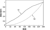
- FIG. 3 is a graph showing a gradation-relative luminance curve in the first embodiment. 8 is a modification of the cross-sectional view of the pixel of the liquid crystal display panel taken along the line BB ′ of FIG.
- FIG. 6 is an upper layer electrode pattern diagram of the liquid crystal display panel according to Embodiment 2. 6 is a micrograph of a liquid crystal display panel according to Embodiment 2.
- FIG. 3 is a diagram illustrating an orientation distribution of liquid crystal molecules of the liquid crystal display panel according to Embodiment 1. 6 is a diagram illustrating a luminance distribution with respect to polar angles of the liquid crystal display panel according to Embodiment 1.
- FIG. FIG. 6 is a diagram illustrating an orientation distribution of liquid crystal molecules of a liquid crystal display panel according to Embodiment 2.
- FIG. 10 is a pixel plan view of a liquid crystal display panel according to a modification of Embodiment 2.
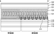
- FIG. 17 is a pixel cross-sectional view of the liquid crystal display panel taken along line EE ′ of FIG. 16.
- 10 is a schematic plan view showing an upper layer electrode of a liquid crystal display panel according to a modification of Embodiment 2.
- FIG. It is a figure which shows the upper layer electrode pattern of the TFT substrate in the liquid crystal display panel of Embodiment 3.
- FIG. 10 is a diagram showing an upper layer electrode pattern of a TFT substrate in a liquid crystal display panel of a modification of Embodiment 3. It is a microscope picture of the upper-layer electrode pattern in the liquid crystal display panel similar to the liquid crystal display panel of the modification of Embodiment 3 except sticking the linearly-polarizing plate. 6 is a micrograph of an upper electrode pattern in a liquid crystal display panel according to a modification of Embodiment 3.
- FIG. 6 is a pixel plan view of a liquid crystal display panel according to Embodiment 4.
- FIG. It is a cross-sectional schematic diagram at the time of the voltage application of the liquid crystal display panel which concerns on the conventional vertical alignment mode (VA mode). It is a graph which shows the gradation-relative luminance curve concerning the conventional VA mode. It is a graph which shows the voltage (V) -relative luminance curve concerning the conventional VA mode. It is a figure when the pixel electrode of the liquid crystal display panel which concerns on the conventional MVA mode is planarly viewed.
- FIG. 30 is a cross-sectional view of the liquid crystal display panel taken along line FF ′ of FIG. 29. It is pixel sectional drawing of the liquid crystal display panel in the case of the conventional TFT side substrate electrode 1 layer.
- a pixel may be a picture element (sub-pixel) unless otherwise specified.
- the planar electrode is a planar electrode in the technical field of the present invention, for example, dot-shaped ribs and / or slits may be formed.
- the planar electrode is also referred to as a solid electrode (a structure having substantially no pattern), and a region where the solid electrode is disposed is also referred to as a solid region or a solid portion.
- the circuit substrate (first substrate) of this embodiment is also referred to as a TFT substrate because it includes a thin film transistor element (TFT).
- FIG. 7 shows the luminance information obtained in the respective areas of the solid portion and the slit portion from the image data and the like shown in FIG. 8, 27, and 28 are measured with a luminance meter “SR-UL1” manufactured by Topcon Corporation. Measurement and observation were both performed at room temperature.
- FIG. 1 is a pixel plan view of the liquid crystal display panel according to the first embodiment, and hatched portions indicate the upper layer electrodes 11 included in the TFT substrate.
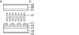
- FIG. 2 is a pixel cross-sectional view of the liquid crystal display panel taken along line AA ′ of FIG.
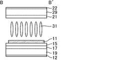
- FIG. 3 is an example of a cross-sectional view of a pixel of the liquid crystal display panel taken along line BB ′ of FIG.
- the counter electrode 21 (third electrode) and the lower layer electrode 17 (second electrode) of the counter substrate shown in FIGS. 2 and 3 are common electrodes, the applied voltage is constant at 0 V, and the upper layer electrode 11 In addition, a voltage of 0 to 5 V is applied to realize a luminance change from a black state to a white state.
- the lower electrode 17 and the counter electrode 21 are preferably in the form of an equipotential.
- the slit region R 1 can also be referred to as comb electrode region where the comb electrodes are arranged.
- the liquid crystal display panel of Embodiment 1 vertically aligns negative (N) liquid crystal 31 when no voltage is applied. Further, when a voltage is applied, an upper electrode 11 (first electrode) formed on the glass substrate 19 (first substrate) and a planar shape formed by sandwiching an insulating layer 15 (Pas) between the upper electrode 11 Liquid crystal molecules by an electric field generated between the lower electrode 17 (second electrode) of the first electrode and the planar electrode (counter electrode 21) formed on the glass substrate 29 (second substrate) facing the first substrate. The amount of transmitted light is controlled by inclining in the horizontal direction.
- the liquid crystal molecules can be suitably tilted in the horizontal direction of the substrate (such as the vertical direction on the paper) when a voltage is applied.
- the insulating layer 15 for example, an oxide film SiO 2 , a nitride film SiN, an acrylic resin, or the like can be used, or a combination of these materials can also be used.
- the polarizing plates 12 and 22 circular polarizing plates are used in the first embodiment.
- FIGS. 2 and 3 show the case where no voltage is applied.
- alignment films are arranged on the liquid crystal layer sides of both substrates, and these alignment films are vertical alignment films that allow liquid crystal molecules to stand perpendicular to the film surfaces. (Either an organic alignment film or an inorganic alignment film may be used). A form in which an alignment auxiliary layer is provided on the alignment film is particularly preferable.
- the alignment auxiliary layer disperses a monomer (monomer) in the liquid crystal, photopolymerizes the monomer dispersed in the liquid crystal by applying light to the liquid crystal while applying a voltage, and an organic polymer ( Polymer), and the initial tilt (pretilt) of the liquid crystal on the alignment film surface is fixed by the polymer.
- the voltage supplied from the video signal line is applied to the upper layer electrode 11 (first electrode) that drives the liquid crystal material through the thin film transistor element (TFT).
- the upper layer electrode 11 (first electrode) and the lower layer electrode 17 (second electrode) are formed in separate layers with the insulating layer 15 interposed therebetween.
- the upper layer electrode 11 (first electrode) is connected to a drain electrode extending from the TFT through a contact hole.
- FIG. 3 shows a state in which the lower layer electrode 17 and the counter electrode 21 have a solid shape, and the upper layer electrode 11 and the upper layer electrode of the adjacent pixel are separated from each other. The same applies to FIGS. 9 and 26 described later.
- the electrode width in the slit region is 2.5 ⁇ m, but is preferably 2.0 ⁇ m or more, for example.
- the upper limit is, for example, 8.0 ⁇ m.
- the ratio (L / S) between the electrode spacing S and the electrode width L is preferably 0.4 to 3, for example.
- a more preferable lower limit value is 0.5, and a more preferable upper limit value is 1.5.
- the cell gap d is set to 2.5 to 4 ⁇ m. It is desirable that the product of the refractive index anisotropy ⁇ n (value for light of wavelength ⁇ ) of the liquid crystal material and the cell gap d substantially satisfies ⁇ / 2.
- the cell gap d thickness of the liquid crystal layer is preferably calculated by averaging all the thicknesses of the liquid crystal layers in the liquid crystal display panel.
- the negative liquid crystal 31 (liquid crystal layer) preferably contains a chiral agent for stabilizing the alignment.
- the chiral agent having a chiral pitch of 120 ⁇ m or less can stabilize the orientation, and the chiral agent having a chiral pitch of 10 ⁇ m or more can substantially not affect the display quality. And more preferable.
- FIG. 4 is a pixel cross-sectional view of the liquid crystal display panel according to the first embodiment.
- a strong lateral electric field is generated in the electrode opening 35.
- the liquid crystal molecules 31 in the electrode openings 35 are not inclined more than the molecules in the electrode portions.
- the electrode structure of the TFT substrate is a single layer as shown in FIG. 31 (only the electrode 611)
- a lateral electric field that is, an equipotential line dent
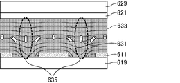
- FIG. 4 an equipotential line 33 is shown, and in FIG. 31, an equipotential line 633 is shown.
- the other reference numbers in FIG. 4 are the same as those shown in FIGS. 2 and 3, and the other reference numbers in FIG. 31 are the same as those shown in FIGS. 2 and 3, except that 6 is added to the hundreds place. It is the same as that.
- the lateral electric field is strong in the electrode opening 35 of FIG. 4, and therefore the tilt of the liquid crystal molecules can be delayed. Therefore, for example, as shown in FIG.
- the VT characteristic can be shifted as compared with the VT characteristic of such a region.
- the electrode of the TFT substrate is a single layer, since the vertical electric field is strong also in the electrode opening 635 of FIG. 31, there is a possibility that the inclination of the liquid crystal molecules is fast and the VT characteristic cannot be sufficiently shifted. .
- FIG. 5 is a pixel plan view of the liquid crystal display panel according to the first embodiment.
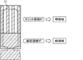
- the pattern of the upper electrode 11 is divided into a slit region R 1 (region having a slit) and a planar region R 2 , the VT characteristics between both regions are greatly shifted, slit region R 1 is a bright region, the planar region R 2 is dark region.
- a multi-VT characteristic similar to that of a TV can be realized, and the number of TFTs can be reduced, for example, as one TFT per pixel. Can be prevented.
- FIG. 6 shows a schematic plan view of a pixel and a micrograph of the liquid crystal display panel according to the first embodiment.
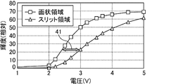
- FIG. 7 is a graph showing a voltage (V) -relative luminance curve in the first embodiment.
- FIG. 8 is a graph showing a gradation-relative luminance curve in the first embodiment.
- V voltage
- FIG. 8 it evaluated after sticking the polarizing plates 12 and 22 (circularly polarizing plate) on the opposite side to the liquid crystal layer side of a glass substrate, respectively.
- the form in which the counter electrode does not have the alignment regulating structure is one of the preferred embodiments of the present invention from the viewpoint of simplicity of panel manufacture and further suppressing reduction in contrast and transmittance.
- the whitening when viewed from an oblique direction is improved as compared with the conventional VA method (conventional structure) which is configured only by a configuration in which liquid crystal molecules are radially arranged (the present invention).
- FIG. 27 showing a gray scale-relative luminance graph in the conventional structure corresponding to FIG. 8.
- FIG. 8 a graph 51 when viewed from an oblique direction and a front view are shown.
- FIG. 27 the luminance difference between the graph 451 when viewed from an oblique direction and the graph 453 when viewed from the front direction is large.
- the liquid crystal display device provided with the liquid crystal display panel of Embodiment 1 can appropriately include a member (for example, a light source or the like) included in a normal liquid crystal display device. The same applies to the embodiments described later.
- FIG. 9 is a modification of the cross-sectional view of the pixel of the liquid crystal display panel taken along line BB ′ of FIG.
- the counter electrode 21 ' has a dot-shaped rib 25'.
- the form in which the counter electrode 21 ′ has an alignment regulating structure such as a point-shaped rib or slit is one preferred embodiment of the present invention. An effect can be exhibited suitably.
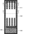
- FIG. 10 is an upper layer electrode pattern diagram of the liquid crystal display panel according to the second embodiment.
- FIG. 11 is a micrograph of the liquid crystal display panel according to the second embodiment.
- the configuration of the second embodiment is the same as the configuration of the first embodiment except that a planar region is formed at the center of the pixel when the upper layer electrode 111 is patterned.
- the cross-sectional structures (layer structures) taken along the lines CC ′ and DD ′ of FIG. 10 are the same as the pixel cross-sectional views of FIGS. 2 and 3 of the first embodiment, respectively.
- FIG. 10 illustrates the TFT area 126 and the contact area 128 (portion for transmitting the source voltage to the upper layer electrode). Since the contact area 128 needs to have a planar electrode structure, the planar structure is arranged in a portion overlapping the light shielding area 124 (shaded portion). The same applies to the other embodiments in this specification.
- the viewing angle characteristics can be further improved when the linear polarizing plate is used.
- the liquid crystal molecules are oriented in the direction along the slit, the liquid crystal molecules are oriented in a direction slightly shifted from the direction along the slit, particularly in the edge portion of the slit.
- the transmission efficiency of is deteriorated.
- the luminance is low in the portion where the liquid crystal molecules are aligned parallel or perpendicular to the absorption axis of the linearly polarizing plate.
- the use of a circularly polarizing plate as in the first embodiment can provide a higher transmittance improvement effect, and can achieve both improvement in transmittance and improvement in viewing angle characteristics.
- the configuration of the second embodiment is the same as that of the first embodiment except for those explicitly described.
- FIG. 12 is a diagram illustrating an orientation distribution of the liquid crystal molecules 31 of the liquid crystal display panel according to the first embodiment.
- FIG. 13 is a diagram illustrating a luminance distribution with respect to the polar angle of the liquid crystal display panel according to the first embodiment.
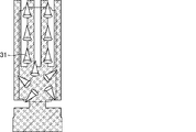
- FIG. 14 is a diagram illustrating an orientation distribution of the liquid crystal molecules 131 of the liquid crystal display panel according to the second embodiment.
- FIG. 15 is a diagram illustrating a luminance distribution with respect to a polar angle of the liquid crystal display panel according to the second embodiment.
- the luminance is high when viewed from the direction of 90 degrees azimuth (FIG. 13). This is because the liquid crystal molecules 31 are tilted in one direction at the slit as shown in FIG.
- the planar region is in the center of the pixel (FIG. 14)
- the luminance distribution is approximately symmetrical vertically (FIG. 15). This is because, as shown in FIG. 14, the directions in which the liquid crystal molecules 131 are inclined in the two slit regions sandwiching the planar region are opposite to each other (vertical direction in FIG. 14). Therefore, it is more desirable to use a pixel pattern that divides the slit region into two parts as in the second embodiment so that the vertically oriented regions are uniform when viewed from the entire pixel (electrode).
- FIG. 16 is a pixel plan view of a liquid crystal display panel according to a modification of the second embodiment, and the hatched portion indicates the upper layer electrode 111 ′ included in the TFT substrate.
- FIG. 17 is a pixel cross-sectional view of the liquid crystal display panel taken along line EE ′ of FIG.
- Such an upper layer electrode pattern is also applicable to the present invention.
- the slit is directed in all directions as in the upper layer electrode pattern described later with reference to FIG. 25, and the orientation dependence of the viewing angle can be more sufficiently eliminated.
- FIG. 17 shows that the potential line 133 in the bright region and the potential line 133 in the dark region are different (in other words, the electric field strength region and the electric lines of force are different between the two regions).
- Other reference numbers are the same as the reference numbers in FIGS. 2 to 4 described above except that 1 is added to the hundreds place.
- FIG. 18 is a schematic plan view showing an upper layer electrode 111 ′′ (shaded portion) of a liquid crystal display panel according to a modification of the second embodiment.
- the linear electrode does not extend from the planar electrode, and there is a possibility that the transmittance equivalent to that of the second embodiment may not be exhibited.
- the effect of the present invention is also exhibited by such a form. Is possible.
- This modification is the same as that of the second embodiment except for the form of the upper layer electrode 111 ′′.
- FIG. 19 is a diagram showing an upper layer electrode pattern of the TFT substrate in the liquid crystal display panel of Embodiment 3.
- FIG. 20 is a micrograph of an upper electrode pattern in a liquid crystal display panel similar to the liquid crystal display panel of Embodiment 3 except that a linearly polarizing plate is attached.
- FIG. 21 is a photomicrograph of the upper electrode pattern in the liquid crystal display panel of Embodiment 3, and this liquid crystal display panel has a circularly polarizing plate attached thereto.
- FIG. 22 is a diagram illustrating an upper layer electrode pattern of a TFT substrate in a liquid crystal display panel according to a modification of the third embodiment.
- FIG. 23 is a photomicrograph of an upper electrode pattern in a liquid crystal display panel similar to the liquid crystal display panel of the modification of Embodiment 3 except that a linearly polarizing plate is attached.
- FIG. 24 is a photomicrograph of an upper electrode pattern in a liquid crystal display panel according to a modification of the third embodiment, and this liquid crystal display panel has a circularly polarizing plate attached thereto.
- the upper layer electrode pattern (shaded portion) shown in FIG. 19 is obtained by closing the upper and lower ends of the slit pattern in the upper layer electrode of the TFT substrate.
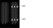
- liquid crystal molecules 231 that fall in opposite directions within the slit pattern are generated due to the influence of an oblique electric field generated at the electrode edge portion when a voltage is applied.
- the orientation defect 232 shown in FIG. 20 may occur.
- the display image is roughened, which may cause deterioration in display quality.
- FIG. 21 there is a possibility that an alignment defect 232 ′ may occur.
- the pattern which concerns on the modification of Embodiment 3 shown in FIG. 22 is a pattern which open
- the liquid crystal molecules 231 ′ are uniformly tilted downward in the slit pattern, so that an image can be displayed without any disturbance.
- FIG. 23 it can be seen that it is particularly desirable to provide a pattern in which one side is opened when the slit region is provided.
- it can be set as embodiment of this invention by applying the pattern shown in Embodiment 3 and its modification to other embodiment.
- FIG. 25 is a pixel plan view of the liquid crystal display panel according to the fourth embodiment.
- the configuration of the liquid crystal display panel according to the fourth embodiment is the same as the configuration of the liquid crystal display panel according to the second embodiment, except that the sub-pixel structure is nearly square as shown in FIG.
- FIG. 25 a light shielding area 324 (shaded portion), a TFT area 326, and a contact area 328 (portion for transmitting a source voltage to the upper layer electrode) are illustrated. Further, the configuration of the fourth embodiment is the same as that of the first embodiment except for the explicit description.
- the structure of the present embodiment has an excellent viewing angle characteristic improving effect.
- the upper layer electrode of the TFT substrate has a region having a plurality of different electrode structures, and this mode is particularly suitable from the viewpoint of the effect, but the lower layer electrode of the TFT substrate has a plurality of electrode structures. May have a structure of different regions.
- the effect is particularly excellent by making the region oriented as a whole of the electrode uniform, aligning the orientation of liquid crystal molecules in each slit region as a pattern in which one side of the slit region is opened, and the like.
- the liquid crystal display device may be a field sequential color system, and in that case, a color filter need not be arranged.
- the material of the semiconductor layer is preferably an oxide semiconductor with high mobility such as IGZO (indium-gallium-zinc-oxygen).
- IGZO indium-gallium-zinc-oxygen
- the size of the TFT element can be reduced as compared with the case of using amorphous silicon, which is suitable for a high-definition liquid crystal display.
- IGZO is preferably used in a method that requires a high-speed response such as a field sequential color method.
Landscapes
- Physics & Mathematics (AREA)
- Nonlinear Science (AREA)
- Liquid Crystal (AREA)
- Spectroscopy & Molecular Physics (AREA)
- Mathematical Physics (AREA)
- Chemical & Material Sciences (AREA)
- Crystallography & Structural Chemistry (AREA)
- General Physics & Mathematics (AREA)
- Optics & Photonics (AREA)
Abstract
本発明は、透過率を充分なものとしながら、白浮きが抑制され、視野角特性に優れる液晶表示パネル及び液晶表示装置を提供する。本発明の液晶表示パネルは、第1基板、第2基板、及び、両基板に挟持された液晶層を備える液晶表示パネルであって、上記第1基板及び第2基板は、それぞれが円偏光板を有し、上記第1基板は、第1電極、第2電極、及び、上記第1電極と上記第2電極との間に挟まれた絶縁層を有し、上記第2基板は、第3電極を有し、上記液晶層は、電圧印加時に、放射状に配向する液晶分子、及び、配向方向が一定方向に揃う液晶分子を含む液晶表示パネルである。
Description
本発明は、液晶表示パネル及び液晶表示装置に関する。より詳しくは、電圧無印加時に基板主面に対して垂直な方向に配向する液晶分子を含む液晶表示パネル及び液晶表示装置に関するものである。
液晶表示パネルは、一対のガラス基板等に液晶表示素子を挟持して構成され、薄型で軽量かつ低消費電力といった特長を活かして、モバイル用途や各種のモニター、テレビ等、日常生活やビジネスに欠かすことのできないものとなっている。近年においては、電子ブック、フォトフレーム、IA(産業機器)、PC(パーソナルコンピュータ)用途等に幅広く採用されている。これらの用途、特に、スマートフォンやタブレットPC等の中小型の携帯用の機器において、液晶層の光学特性を変化させるための電極配置や基板の設計に係る各種モードの液晶表示パネルが検討されている。
例えば、多数の画素を含む液晶表示装置であって、対向する第1基板及び第2基板と、前記第1基板上に形成されている第1電極と、前記第1基板上に前記第1電極と絶縁して形成されており、前記第1電極と少なくとも一部分が重畳しており、前記第1電極間で連続的な面からなる第2電極を含み、一つの画素は少なくとも前記第1電極のうちの一つと第2電極とを含む液晶表示装置が開示されている(例えば、特許文献1参照。)。
上述した特許文献1は、基本的なFFS(Fringe Field Switching)電極構造(くし歯電極/絶縁層/面状の電極〔ベタ電極〕/基板)に様々な変化(電極の配置や液晶材料の誘電異方性の違い)を付与することで、広視野角・低電圧駆動を実現するというものである(例えば、第18実施例の断面図(特許文献1の図96)を参照。)。
しかしながら、特許文献1に記載の液晶表示装置には、透過率を充分なものとしながら、視野角特性を優れたものとすることができないという課題があった。
また近年のモバイル機器では広視野角特性が求められているが、従来のVAモード等においては、液晶表示装置を斜めから観察した際に、顕著な白浮きが発生し、表示品位を劣化させるという課題があった。
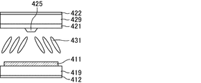
白浮きの理由を以下に説明する。図26は、従来の垂直配向モード(VAモード)に係る液晶表示パネルの電圧印加時の断面模式図である。従来の垂直配向モードでは、図26に示されるように、液晶分子を放射状に配列させる構成のみからなる方式を採用しており、配向規制構造体であるリブ425を中心として液晶分子が放射状に配向している。なお、図26では、ガラス基板419、429、TFT基板側の絵素電極411、対向電極421、偏光板412、422、液晶431を図示している。また、図27は、従来のVAモードに係る階調-相対輝度曲線を示すグラフである。図28は、従来のVAモードに係る電圧(V)-相対輝度曲線を示すグラフである。例えば、図27におけるように、斜めから見た場合のグラフ451は、正面から見た場合のグラフ453と比べて、同じ階調で輝度が高くなる程度が大きいため、白浮きが発生する。図28における白丸で示した斜めから見た場合のグラフ、黒丸で示した正面から見た場合のグラフについても同様である。
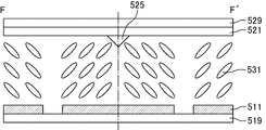
ところで、図29は、従来のMVAモードに係る液晶表示パネルの絵素電極511を平面視したときの図である。図30は、図29のF-F′線に沿った液晶表示パネルの断面図である。一対のガラス基板519、529に挟持された液晶分子531は、ガラス基板529に配置されたリブ525及びガラス基板519に配置された絵素電極511を境目として液晶分子が配向するが、視野角特性の観点からは、画素単位で補償を行うものであり、個々の電極単位で補償を行うものではなかった。
従来、VAモードの視野角改善技術としては、MPD(Multi Pixel Driving)駆動が使用されてきた。この技術によれば、1サブ画素の中に独立して駆動する2つの領域を形成し、それぞれを明画素、暗画素として駆動する形態とすることにより、上記白浮きを低減できるというものである。1サブ画素の中に異なるVT曲線(電圧-透過率曲線)を有する領域が複数あることから、本明細書中、このような形態をマルチVTともいう。しかしながら、従来のマルチVT技術においては、それぞれの領域を駆動するために少なくとも1つのトランジスタが必要となり、1サブ画素を駆動するために少なくとも2つのトランジスタが必要になるため、開口率(透過率)の大きな低減を招いていた。すなわち、VAモードにおいて、透過率を充分なものとしながら、白浮きを抑制し、視野角特性を改善するための工夫の余地があった。
本発明は、上記現状に鑑みてなされたものであり、透過率を充分なものとしながら、白浮きを抑制し、視野角特性を優れたものとした液晶表示パネル及び液晶表示装置を提供することを目的とするものである。
本発明者らは、VAモード等において、透過率を充分なものとしながら、視野角特性を改善することができる液晶表示パネル及び液晶表示装置について種々検討したところ、VAモードの液晶表示パネル及び液晶表示装置は、液晶表示パネルを斜め方向から観察した際に、正面から見た場合と比べて、VT特性が異なり、同じ印加電圧での輝度がより高くなることに着目した。そして、少なくとも2つ以上のVT特性の異なる領域を作り、透過率を充分なものとしながら白浮きの発生を抑制して視野角特性を改善することができること、更に、円偏光板を用いることにより、透過率を向上させることができ、優れた透過率と視野角特性とを両立することができることを見いだし、上記課題をみごとに解決することができることに想到し、本発明に到達したものである。
すなわち、本発明は、第1基板、第2基板、及び、両基板に挟持された液晶層を備える液晶表示パネルであって、上記第1基板及び第2基板は、それぞれが円偏光板を有し、上記第1基板は、第1電極、第2電極、及び、上記第1電極と上記第2電極との間に挟まれた絶縁層を有し、上記第2基板は、第3電極を有し、上記液晶層は、電圧印加時に、放射状に配向する液晶分子、及び、配向方向が一定方向に揃う液晶分子を含む液晶表示パネルである。
上記液晶層が、電圧印加時に、放射状に配向する液晶分子、及び、配向方向が一定方向に揃う液晶分子を含むとは、言い換えれば、上記液晶層は、電圧印加時に、液晶分子が放射状に配向する領域、及び、液晶分子の配向方向が一定方向に揃う領域を含むことをいう。放射状に配向するとは、基板主面を平面視したときに一点を中心として全水平方向に配向するものであることが好適である。また、放射状に配向する領域が、それ自体で視野角が補償されるものであることが好ましい。
上記配向方向が一定方向に揃うとは、液晶分子の配向方向が、平均的に見た場合に一定方向を向いている限り、個々の液晶分子の配向方向が、おおよそ一定方向に揃うものであればよい。また、通常は、基板主面を平面視したときに一水平方向に配向するものをいう。配向方向が一定方向に揃う領域は、通常はそれ自体で視野角が補償されるものではないが、1つの電極全体で視野角が補償されるものであることが好ましい。
本発明の液晶表示パネルは、第1基板及び第2基板のそれぞれが円偏光板を有する。このような構成により、透過率改善効果を発揮することができ、これにより、本発明の液晶表示パネルは透過率と視野角の両方に優れるものとなる。
上記液晶層は、電圧印加時に、複数の異なる電界強度領域及び/又は複数の異なる電気力線領域を有することが好ましい。電界強度領域及び/又は電気力線領域が異なるとは、その向き、強度のいずれか少なくとも1つが異なり、本発明の効果が発揮されるといえるものであればよい。言い換えれば、上記液晶層は、電圧印加時に、複数の異なる電界領域を有することが好ましい。
上記液晶層は、電圧無印加時に基板主面に対して垂直な方向に配向する液晶分子を含むことが好ましい。電圧無印加時とは、本発明の技術分野において、電圧が実質的に無印加であるといえる形態を含むものである。なお、電圧は、通常は、第1基板が有する第1電極及び第2電極のうち、液晶層側の電極に対して印加する。また、基板主面に対して垂直方向に配向するとは、本発明の技術分野において、基板主面に対して垂直方向に配向するといえるものであればよく、実質的に垂直方向に配向する形態を含むものである。
上記第1電極及び上記第2電極の少なくとも一方は、複数の電極構造が異なる領域を有することが好ましい。電極構造が異なるとは、本発明の作用効果が発揮されるといえる程度に異なるものであればよい。例えば、上記第1電極及び上記第2電極の少なくとも一方が、複数の線状の電極構造をもつ領域と、面状の電極構造をもつ領域とを有することが好ましい。具体的には、例えば、(1)上層電極の一部をパターニングし、液晶駆動電圧を印加する形態(例えば、図1に示すように、スリットが形成された電極が配置される暗領域R1と面状電極が配置される明領域R2とに分ける。)、及び/又は、(2)下層電極を実質的にパターンの無い構造(ベタ)とし、対向側電極と同電位を印加する形態とすることが好ましい。これらの電極構造により、簡便に本発明の作用効果を発揮することができる。
本発明の液晶表示パネルは、基板主面を平面視したときに、上記線状電極がそれぞれ略平行であることが好ましい。また、上記第1電極は、基板主面を平面視したときに、複数の略平行なスリットを有することが特に好ましい。例えば、複数の略平行なスリットを有する領域と面状の領域とをもつ電極(第1電極)の下層(第1基板からみて液晶層と反対側の層)に絶縁層を介して面状の電極(第2電極)を設ける形態が特に好ましい。また、本発明の液晶表示パネルは、基板主面を平面視したときに、上記面状電極から線状電極が延びている形態が好ましい。この形態により、配向欠陥(液晶分子同士がぶつかり合って倒れることが出来ない領域)を小さくし、透過率をより高め、かつ画像表示のざらつきを抑えることができる。
電界を好適に制御するうえでは、複数の略平行なスリットを有する領域と面状の領域とをもつ電極が、液晶層側の電極(上層電極)であることが好ましい。また、上記複数の略平行なスリットを有する領域と面状の領域とをもつ電極とは、その面積比が、5:1~1:2であることが好ましい。より好ましくは、3:1~1:1である。
上記複数の略平行なスリットを有する領域は、例えば、くし歯電極を有する領域であることが好ましい。くし歯電極における歯部分の幅は、例えば0.5μm~5μmであることが好ましい。また、上記スリットの幅は、例えば0.5μm~5μmであることが好ましい。上記面状の領域としては、リブ又はスリットのいずれも有さない形態、中心部分だけに配向規制構造体を有する形態等が挙げられる。
上記第1基板及び第2基板は、少なくとも一方に、垂直配向膜を有し、該垂直配向膜上に配向補助層が設けられていることが好ましい。配向補助層とは、例えば、有機重合体である。
上記第3電極は、配向規制構造体を有することが本発明の好ましい形態の一つである。配向規制構造体とは、リブ及び/又はスリットであることが好ましい。例えば、上記第3電極の中心部分だけに配向規制構造体が形成される形態が好ましい。また、上記第3電極は、面状であることが好ましい。第3電極が面状であるとは、例えば、図10のコンタクトエリアや、TFTエリアを横断するように、電極に開口部が設けてある形態であってもよいが、少なくとも、基板主面を平面視したときに第1電極と重畳する箇所が面状であることが好ましい。
本発明の液晶表示パネルにおいては、第1電極には0Vを超えるか、又は、0V未満の電位を与え、第2電極及び第3電極は、第1電極とは反対極性であって、互いに同極性の電位を与える(0Vでもよい)。第1電極の電位と、第2電極の電位又は第3電極の電位とは、異なっていてもよい。また、第2電極の電位と第3電極の電位とは、同じであってもよく、異なっていてもよい。第2電極の電位と第3電極の電位とが同じであるとは、本発明の技術分野において、実質的に同じであるといえるものであればよい。また、上記液晶層は、正の誘電率異方性を有する液晶分子を含んでいてもよいが、通常は負の誘電率異方性を有する液晶分子(ネガ型液晶材料)を含むものであり、負の誘電率異方性を有する液晶分子から実質的に構成されることが好ましい。このようにすることで、電圧無印加時において、液晶層にはネガ型液晶材料を垂直配向させる。
なお、画素電極及び共通電極が配置された基板が、アクティブマトリクス基板であることが好適である。また、本発明の液晶表示パネルは、透過型、反射型、半透過型のいずれであってもよい。
本発明はまた、本発明の液晶表示パネルを備える液晶表示装置でもある。
本発明の液晶表示装置における液晶表示パネルの好ましい形態は、上述した本発明の液晶表示パネルの好ましい形態と同様である。液晶表示装置としては、電子ブック、フォトフレーム、IA(産業機器)、PC(パーソナルコンピュータ)用途等が挙げられ、特に、スマートフォンやタブレットPC等の中小型の機器、携帯用の機器に適用されることが好ましい。
本発明の液晶表示装置における液晶表示パネルの好ましい形態は、上述した本発明の液晶表示パネルの好ましい形態と同様である。液晶表示装置としては、電子ブック、フォトフレーム、IA(産業機器)、PC(パーソナルコンピュータ)用途等が挙げられ、特に、スマートフォンやタブレットPC等の中小型の機器、携帯用の機器に適用されることが好ましい。
本発明の液晶表示パネル及び液晶表示装置の構成としては、このような構成要素を必須として形成されるものである限り、その他の構成要素により特に限定されるものではなく、液晶表示パネル及び液晶表示装置に通常用いられるその他の構成を適宜適用することができる。
上述した各形態は、本発明の要旨を逸脱しない範囲において適宜組み合わされてもよい。
本発明の液晶表示パネル及び液晶表示装置によれば、第1基板及び第2基板がそれぞれ円偏光板を有し、液晶層が、電圧印加時に、放射状に配向する液晶分子、及び、配向方向が一定方向に揃う液晶分子を含むことにより、透過率を充分なものとしながら、白浮きが抑制され、視野角特性に優れるものとすることができる。
以下に実施形態を掲げ、本発明を図面を参照して更に詳細に説明するが、本発明はこれらの実施形態のみに限定されるものではない。本明細書中、画素とは、特に明示しない限り、絵素(サブ画素)であってもよい。本明細書中、面状電極は、本発明の技術分野において面状電極であるといえる限り、例えば、点形状のリブ及び/又はスリットが形成されていてもよい。面状電極は、ベタ電極(実質的にパターンの無い構造)ともいい、ベタ電極が配置される領域をベタ領域又はベタ部分等ともいう。本実施形態の回路基板(第1基板)を、薄膜トランジスタ素子(TFT)を有することから、TFT基板ともいう。
図4及び図31は、Shintech社製配向シミュレータ「LCDMaster」で計算したものである。図6、図11、図20、図21、図23及び図24は、ニコン社製顕微鏡「LM-1270TE」にて画像を撮影したものである。図7は、図6に示した画像データ等より、ベタ部及びスリット部のそれぞれの領域における輝度情報を取得したものである。図8、図27及び図28は、トプコン社製輝度計「SR-UL1」にて測定したものである。なお、測定・観察はいずれも室温環境下にて行った。
(実施形態1)
本発明による技術を適応した構造でパネル試作を行った。図1は、実施形態1に係る液晶表示パネルの画素平面図であり、斜線部はTFT基板が有する上層電極11を示す。図2は、図1のA-A′線に沿った液晶表示パネルの画素断面図である。図3は、図1のB-B′線に沿った液晶表示パネルの画素断面図の一例である。図1に示した上層電極11は、それぞれ点線で囲ったスリット領域R1と面状領域R2とを有し、スリット領域R1と面状領域R2との面積比は、2:1となるように設計している。図2、図3に示した対向基板が有する対向電極21(第3電極)及び下層電極17(第2電極)は、共通(Common)電極としており、印加電圧は0Vで一定とし、上層電極11に、0~5Vまでの電圧を印加し、黒状態~白状態までの輝度変化を実現する。なお、下層電極17及び対向電極21は等電位とする形態が好ましいが、本発明の要旨を逸脱しない限り、下層電極17(第2電極)の電位と対向電極21(第3電極)の電位とは異なっていてもよい。また、スリット領域R1は、くし歯電極が配置されたくし歯電極領域ということもできる。
本発明による技術を適応した構造でパネル試作を行った。図1は、実施形態1に係る液晶表示パネルの画素平面図であり、斜線部はTFT基板が有する上層電極11を示す。図2は、図1のA-A′線に沿った液晶表示パネルの画素断面図である。図3は、図1のB-B′線に沿った液晶表示パネルの画素断面図の一例である。図1に示した上層電極11は、それぞれ点線で囲ったスリット領域R1と面状領域R2とを有し、スリット領域R1と面状領域R2との面積比は、2:1となるように設計している。図2、図3に示した対向基板が有する対向電極21(第3電極)及び下層電極17(第2電極)は、共通(Common)電極としており、印加電圧は0Vで一定とし、上層電極11に、0~5Vまでの電圧を印加し、黒状態~白状態までの輝度変化を実現する。なお、下層電極17及び対向電極21は等電位とする形態が好ましいが、本発明の要旨を逸脱しない限り、下層電極17(第2電極)の電位と対向電極21(第3電極)の電位とは異なっていてもよい。また、スリット領域R1は、くし歯電極が配置されたくし歯電極領域ということもできる。
実施形態1の液晶表示パネルは、図2、図3に示されるように、電圧無印加時にはネガ(N)型液晶31を垂直配向させる。また、電圧印加時にはガラス基板19(第1基板)上に形成された上層電極11(第1電極)、及び、上層電極11との間に絶縁層15(Pas)を挟んで形成された面状の下層電極17(第2電極)と、第1基板の対向するガラス基板29(第2基板)上に形成された面状電極(対向電極21)との間に発生する電界で、液晶分子を水平方向に傾斜させることによって透過光量を制御する。ネガ型液晶31を使用することで、電圧印加時に液晶分子を基板水平方向(紙面垂直方向等)に好適に倒すことができる。絶縁層15には、例えば、酸化膜SiO2や、窒化膜SiNや、アクリル系樹脂等が使用され、または、それらの材料の組み合わせも使用可能である。偏光板12、22としては、実施形態1では円偏光板を用いた。
上述したように、図2、図3は、電圧無印加時の場合を示している。図2、図3には示していないが、両基板の液晶層側にはそれぞれ配向膜が配置され、これら配向膜には、膜面に対して液晶分子を垂直に立たせるような垂直配向膜を用いる(有機配向膜又は無機配向膜のいずれでもよい)。また、配向膜上に、配向補助層が設けられている形態が特に好ましい。配向補助層は、液晶中に単量体(モノマー)を分散させ、液晶に電圧を印加しながら光照射することにより液晶中に分散させたモノマーを光重合させ、配向膜表面に有機重合体(ポリマー)を形成し、この重合体により配向膜表面の液晶の初期傾斜(プレチルト)を固定化する。
走査信号線で選択されたタイミングで、映像信号線から供給された電圧を薄膜トランジスタ素子(TFT)を通じて、液晶材料を駆動する上層電極11(第1電極)に印加する。なお、上層電極11(第1電極)と下層電極17(第2電極)とは、絶縁層15を介して別層に形成されている。上層電極11(第1電極)はコンタクトホールを介してTFTから伸びているドレイン電極と接続されている。なお、図3では、下層電極17や対向電極21がベタ形状であり、上層電極11と隣の画素の上層電極との間が離れている様子が示されている。後述する図9、図26においても同様である。
本実施形態では、スリット領域における電極幅は2.5μmであるが、例えば2.0μm以上が好ましい。なお、上限値は、例えば8.0μmである。線状電極の電極間隔(スリットの幅)の好ましい範囲も同様である。
また、電極間隔Sと電極幅Lとの比(L/S)としては、例えば0.4~3であることが好ましい。より好ましい下限値は、0.5であり、より好ましい上限値は、1.5である。
また、電極間隔Sと電極幅Lとの比(L/S)としては、例えば0.4~3であることが好ましい。より好ましい下限値は、0.5であり、より好ましい上限値は、1.5である。
セルギャップdについては、2.5~4μmとする。液晶材料の屈折率異方性Δn(波長λの光に対する値)とセルギャップdの積がほぼλ/2を満たすことが望ましい。セルギャップd(液晶層の厚み)は、本明細書中、液晶表示パネルにおける液晶層の厚みの全部を平均して算出されるものであることが好ましい。
また、面状領域部の配向安定化を図るため、ピッチ60μmとなるようにカイラル剤を混入したネガ型液晶材料をパネルに注入した。このように、ネガ型液晶31(液晶層)は、配向安定化のためのカイラル剤を含むことが好ましい。中でも、カイラルピッチ120μm以下のカイラル剤であれば、配向を安定化させることができるとともにカイラルピッチ10μm以上のカイラル剤であれば、表示品位に実質的に影響を及ぼさないものとすることができる点でより好ましい。
図4は、実施形態1に係る液晶表示パネルの画素断面図である。図4に示したように、TFT基板を2層電極構造とした場合、電極開口部35において強い横電界が発生する。このとき、電極開口部35の液晶分子31は電極部の分子よりも傾斜しない。より強い電圧を上層電極11に印加した場合は、電極開口部35の液晶分子31も充分傾斜させることができる。一方、図31に示したようにTFT基板の電極構造が1層の場合(電極611のみ)、電圧印加時に電極開口部635において横電界(すなわち等電位線のへこみ)が発生するが、それよりも縦方向の電界が強いため、電極部だけでなく電極開口部635においても、液晶分子631は充分に傾斜する。なお、図4中、等電位線33が示され、図31中、等電位線633が示されている。図4のその他の参照番号は、図2、図3において示したのと同様であり、図31のその他の参照番号は、百の位に6を付した以外は、図2、図3に示したのと同様である。
つまり、TFT基板の電極が2層の場合は、図4の電極開口部35において横電界が強いため、液晶分子の傾斜を遅らせることができ、したがって、例えば図3に示すように上層電極がベタであるような領域のV-T特性に比べて、V-T特性をシフトさせることができる。一方、TFT基板の電極が1層の場合は、図31の電極開口部635においても縦電界が強いため、液晶分子の傾斜が速く、V-T特性を充分にシフトさせることができないおそれがある。
図5は、実施形態1に係る液晶表示パネルの画素平面図である。図5に示すように、上層電極11のパターンをスリット領域R1(スリットをもつ領域)と面状領域R2とに分けた場合、後に詳しく示すように、両領域間でV-T特性は大きくシフトし、スリット領域R1が明領域、面状領域R2が暗領域となる。これにより、TV同様のマルチVT特性を実現できるとともに、例えば1画素当たり1つのTFT等として、TFT数を削減し、従来のMPD技術における課題であった透過率(開口率)の低下を充分に防止できる。
本実施形態に係るパネルの評価結果を図6~図8に示す。図6は、実施形態1に係る液晶表示パネルの画素平面模式図及び顕微鏡写真を示す。図7は、実施形態1における電圧(V)-相対輝度曲線を示すグラフである。図8は、実施形態1における階調-相対輝度曲線を示すグラフである。なお、図4等に示した断面構造のように、ガラス基板の液晶層側と反対側のそれぞれに偏光板12、22(円偏光板)を貼り付けたうえで評価を行っている。
図6に示した電圧印加時の画素の観察より、上層電極11への印加電圧(写真の上に示す)の増加に伴い、面状領域R2が先に明るくなり、スリット領域R1は遅れて明るくなっていることがわかる。すなわち、1画素内で明/暗領域を実現している。また、図7のグラフのように、三角で示したスリット領域(暗領域)のV-T特性のグラフと四角で示した面状領域(明領域)のV-T特性のグラフから、両領域間でV-T特性のシフト41があることを確認した。なお、図6の写真では面状領域R2の中心に光が透過しない点があるが、対向電極の形態は図3に示した通りであり、対向電極の対応する箇所に配向規制構造体が存在する訳ではない。このように対向電極が配向規制構造体を有さない形態が、パネル作製の簡便さ、さらにコントラストや透過率の低下を抑えるという観点から、本発明の好ましい実施形態の1つである。
本発明による技術を適用することにより、従来の、液晶分子を放射状に配列させる構成のみからなるVA方式(従来構造)に比べて、斜め方向から見たときの白浮きが改善される(本発明による技術を適用した図8、及び、図8に対応する、従来構造における階調-相対輝度のグラフを示す図27参照。図8では、斜め方向から見たときのグラフ51と正面方向から見たときのグラフ53との輝度差が小さいが、図27では、斜め方向から見たときのグラフ451と正面方向から見たときのグラフ453との輝度差が大きくなっている)。
なお、実施形態1の液晶表示パネルを備える液晶表示装置は、通常の液晶表示装置が備える部材(例えば、光源等)を適宜備えることができる。後述する実施形態においても同様である。
図9は、図1のB-B′線に沿った液晶表示パネルの画素断面図の変形例である。図9では、対向電極21′が点形状のリブ25′を有する。このように、対向電極21′が、点形状のリブ、スリット等の配向規制構造体を有する形態が本発明の一つの好適な実施形態であり、これにより配向を好適に調整して本発明の効果を好適に発揮することができる。
(実施形態2)
図10は、実施形態2に係る液晶表示パネルの上層電極パターン図である。図11は、実施形態2に係る液晶表示パネルの顕微鏡写真である。実施形態2の構成は、上層電極111のパターニングの際に、面状領域を画素中央部へ形成した以外は、実施形態1の構成と同様である。なお、図10のC-C′、D-D′における断面構造(層構造)は、それぞれ、実施形態1の図2、図3の画素断面図と同様である。図10では、TFTエリア126とコンタクトエリア128(ソース電圧を上層電極へ伝達する部分)を図示している。コンタクトエリア128の部分は面状電極構造にしておく必要があるため、遮光エリア124(斜線部分)に重なる部分に面状構造を配置している。本明細書中のその他の実施形態においても同様である。
図10は、実施形態2に係る液晶表示パネルの上層電極パターン図である。図11は、実施形態2に係る液晶表示パネルの顕微鏡写真である。実施形態2の構成は、上層電極111のパターニングの際に、面状領域を画素中央部へ形成した以外は、実施形態1の構成と同様である。なお、図10のC-C′、D-D′における断面構造(層構造)は、それぞれ、実施形態1の図2、図3の画素断面図と同様である。図10では、TFTエリア126とコンタクトエリア128(ソース電圧を上層電極へ伝達する部分)を図示している。コンタクトエリア128の部分は面状電極構造にしておく必要があるため、遮光エリア124(斜線部分)に重なる部分に面状構造を配置している。本明細書中のその他の実施形態においても同様である。
図11に示した顕微鏡写真より、実施形態1の場合と同様に、円偏光板を貼った場合においてマルチVTとなっていることを確認した。なお、直線偏光板を貼った場合(直線偏光板を貼った以外は実施形態2と同様の液晶表示パネルにおける上層電極パターンの顕微鏡写真)においても、面状領域とスリット領域との間でマルチVTとなっていることがわかる。
なお、直線偏光板を使用した場合の方が、視野角特性をより優れたものとすることができる。一方では、スリットを有する領域においては、液晶分子はおおよそスリットに沿う方向へ向いているものの、特にスリットのエッジの部分では、液晶分子はスリットに沿う方向からややずれた方向へ配向するため、光の透過効率が悪くなる。また、ベタ電極の領域においても、図11より明らかなように、直線偏光板の吸収軸と平行もしくは垂直に液晶分子が配向する部分においては、輝度が低くなる。
このため、実施形態1のように円偏光板を使用した方が高い透過率改善効果をだすことができ、透過率の向上と視野角特性の改善とを両立することができる。なお、実施形態2は、明示した以外の構成は、実施形態1と同様である。
このため、実施形態1のように円偏光板を使用した方が高い透過率改善効果をだすことができ、透過率の向上と視野角特性の改善とを両立することができる。なお、実施形態2は、明示した以外の構成は、実施形態1と同様である。
(配向分布及び極角に対する輝度分布の比較)
図12~図15に、実施形態1及び実施形態2に係る液晶分子の配向分布および極角に対する輝度分布を示し、両実施形態を比較する。図12は、実施形態1に係る液晶表示パネルの液晶分子31の配向分布を示す図である。図13は、実施形態1に係る液晶表示パネルの極角に対する輝度分布を示す図である。図14は、実施形態2に係る液晶表示パネルの液晶分子131の配向分布を示す図である。図15は、実施形態2に係る液晶表示パネルの極角に対する輝度分布を示す図である。
図12~図15に、実施形態1及び実施形態2に係る液晶分子の配向分布および極角に対する輝度分布を示し、両実施形態を比較する。図12は、実施形態1に係る液晶表示パネルの液晶分子31の配向分布を示す図である。図13は、実施形態1に係る液晶表示パネルの極角に対する輝度分布を示す図である。図14は、実施形態2に係る液晶表示パネルの液晶分子131の配向分布を示す図である。図15は、実施形態2に係る液晶表示パネルの極角に対する輝度分布を示す図である。
実施形態1のように面状領域が画素下側にある場合(図12)は、方位90度方向から見たときの輝度が高くなっている(図13)。これは、図12に示されるように、スリット部において液晶分子31が一方向に傾斜する為である。一方、面状領域が画素中央にある場合(図14)、輝度分布はおおよそ上下対称となっている(図15)。これは、図14に示されるように、面状領域を挟む2つのスリット領域において液晶分子131が傾斜する向きが互いに反対方向(図14での上下方向)である為である。したがって、画素(電極)全体で見て、上下に配向する領域が均等になるように、実施形態2のようにスリット領域を2分する画素パターンにすることがより望ましい。
図16は、実施形態2の変形例に係る液晶表示パネルの画素平面図であり、斜線部はTFT基板が有する上層電極111′を示す。図17は、図16のE-E′線に沿った液晶表示パネルの画素断面図である。このような上層電極パターンも本発明に適用可能である。この上層電極パターンの場合、後述する図25に記載の上層電極パターンのように、スリットが四方へ向いており、視野角の方位依存をより充分に解消することができる。なお、図17は、明領域の電位線133と暗領域の電位線133が異なる(言い換えれば、両領域間で電界強度領域及び電気力線が異なる)ことを示す。その他の参照番号は、百の位に1を付した以外は、上述した図2~図4における参照番号と同様である。
図18は、実施形態2の変形例に係る液晶表示パネルの上層電極111′′(斜線部)を示す平面模式図である。このような形態は、面状電極から線状電極が延びている訳ではなく、実施形態2と同等の透過率を発揮できないおそれがあるが、このような形態によっても、本発明の効果を発揮することが可能である。この変形例は、上層電極111′′の形態以外は、実施形態2と同様である。
(実施形態3)
図19は、実施形態3の液晶表示パネルにおけるTFT基板の上層電極パターンを示す図である。図20は、直線偏光板を貼り付けた以外は実施形態3の液晶表示パネルと同様の液晶表示パネルにおける上層電極パターンの顕微鏡写真である。図21は、実施形態3の液晶表示パネルにおける上層電極パターンの顕微鏡写真であり、この液晶表示パネルは円偏光板を貼り付けたものである。図22は、実施形態3の変形例の液晶表示パネルにおけるTFT基板の上層電極パターンを示す図である。図23は、直線偏光板を貼り付けた以外は実施形態3の変形例の液晶表示パネルと同様の液晶表示パネルにおける上層電極パターンの顕微鏡写真である。図24は、実施形態3の変形例の液晶表示パネルにおける上層電極パターンの顕微鏡写真であり、この液晶表示パネルは円偏光板を貼り付けたものである。
図19は、実施形態3の液晶表示パネルにおけるTFT基板の上層電極パターンを示す図である。図20は、直線偏光板を貼り付けた以外は実施形態3の液晶表示パネルと同様の液晶表示パネルにおける上層電極パターンの顕微鏡写真である。図21は、実施形態3の液晶表示パネルにおける上層電極パターンの顕微鏡写真であり、この液晶表示パネルは円偏光板を貼り付けたものである。図22は、実施形態3の変形例の液晶表示パネルにおけるTFT基板の上層電極パターンを示す図である。図23は、直線偏光板を貼り付けた以外は実施形態3の変形例の液晶表示パネルと同様の液晶表示パネルにおける上層電極パターンの顕微鏡写真である。図24は、実施形態3の変形例の液晶表示パネルにおける上層電極パターンの顕微鏡写真であり、この液晶表示パネルは円偏光板を貼り付けたものである。
図19に示した上層電極パターン(斜線部)は、TFT基板の上層電極において、スリットパターンの上下端を閉じたものである。この場合、電圧印加時に電極エッジ部に発生する斜め電界の影響により、スリットパターン内で相反する方向へ倒れる液晶分子231が発生する。このため、図20に示される配向欠陥232が発生するおそれがある。このような配向欠陥が発生した場合、表示画像にざらつきが発生し、表示品位の劣化を招くおそれがある。図21においても同様に、配向欠陥232′が発生するおそれがある。
一方、図22に示した実施形態3の変形例に係るパターンは、実施形態1、2と同様に、スリットパターンの上端を開放したパターンである。この場合、図23に示されるように、電圧印加時に液晶分子231′はスリットパターン内で下方向へ一様に傾斜するため、乱れの無い画像表示が可能となる。図24においても同様である。したがって、スリット領域を設ける際には、その片側を開放したパターンにすることが特に望ましいことが分かる。
なお、実施形態3及びその変形例に示したパターンをその他の実施形態に適用することにより、本発明の実施形態とすることができる。
なお、実施形態3及びその変形例に示したパターンをその他の実施形態に適用することにより、本発明の実施形態とすることができる。
(実施形態4)
図25は、実施形態4に係る液晶表示パネルの画素平面図である。実施形態4に係る液晶表示パネルの構成は、図25に示したようにサブ画素構造が正方形に近い形になっている以外は、実施形態2に係る液晶表示パネルの構成と同様である。それぞれのサブ画素中央の上層電極311の面状部分R2に対し、スリットを四方へ伸ばすこと、言い換えれば、四つの方向に線状電極R1が延びていることにより、視角方向を変えたときの(色々な方向から見たときの)変化がより少なく、視野特性をより優れたものとすることができる。
図25は、実施形態4に係る液晶表示パネルの画素平面図である。実施形態4に係る液晶表示パネルの構成は、図25に示したようにサブ画素構造が正方形に近い形になっている以外は、実施形態2に係る液晶表示パネルの構成と同様である。それぞれのサブ画素中央の上層電極311の面状部分R2に対し、スリットを四方へ伸ばすこと、言い換えれば、四つの方向に線状電極R1が延びていることにより、視角方向を変えたときの(色々な方向から見たときの)変化がより少なく、視野特性をより優れたものとすることができる。
なお、図25では、遮光エリア324(斜線部分)、TFTエリア326及びコンタクトエリア328(ソース電圧を上層電極へ伝達する部分)を図示している。また、実施形態4は、明示した以外の構成は、実施形態1と同様である。
よって、本実施形態の構造においては、いずれも優れた視野角特性改善効果を得ることが分かった。なお、本実施形態では、TFT基板の上層電極が複数の電極構造が異なる領域を有する形態であり、当該形態が作用効果の点から特に好適であるが、TFT基板の下層電極が複数の電極構造が異なる領域の構造を有する形態であってもよい。また、電極全体として配向する領域を均等とすること、スリット領域の片側を開放したパターンとしてスリット領域毎に液晶分子の配向の向きを揃えること等により、当該効果に特に優れることが分かった。
本実施形態に係る液晶表示装置は、フィールドシーケンシャルカラー方式であってもよく、その場合、カラーフィルタは配置される必要はない。
TFT基板のTFTにおいて、半導体層の材料としては、IGZO(インジウム-ガリウム-亜鉛-酸素)等の、移動度の高い酸化物半導体が好ましい。IGZOを用いることで、アモルファスシリコンを用いる場合と比べてTFT素子のサイズを小さくすることができるため、高精細な液晶ディスプレイに適している。特に、フィールドシーケンシャルカラー方式のように高速応答が求められる方式においては、IGZOが好適に用いられる。
上述した実施形態における各形態は、本発明の要旨を逸脱しない範囲において適宜組み合わされてもよい。
なお、本願は、2010年12月28日に出願された日本国特許出願2010-293852号を基礎として、パリ条約ないし移行する国における法規に基づく優先権を主張するものである。該出願の内容は、その全体が本願中に参照として組み込まれている。
11、11′、111、111′、111′′、311、611:上層電極
12、12′22、22′、422:偏光板
15、15′:絶縁層
17、17′:下層電極
19、19′、29、29′、419、429、519、529、619、629:ガラス基板
21、21′、421、621:対向電極
25′、425、525:リブ
31、31′、131、231、231′、431、531、631:液晶(液晶分子)
33、633:等電位線
34、134、234:等電位線
35、635:電極開口部
41:V-T特性のシフト
51、451:斜めから見た場合のグラフ
53、453:正面から見た場合のグラフ
124:遮光エリア
126、326:TFTエリア
128、328:コンタクトエリア
232、232′:配向欠陥
411、511:絵素電極
12、12′22、22′、422:偏光板
15、15′:絶縁層
17、17′:下層電極
19、19′、29、29′、419、429、519、529、619、629:ガラス基板
21、21′、421、621:対向電極
25′、425、525:リブ
31、31′、131、231、231′、431、531、631:液晶(液晶分子)
33、633:等電位線
34、134、234:等電位線
35、635:電極開口部
41:V-T特性のシフト
51、451:斜めから見た場合のグラフ
53、453:正面から見た場合のグラフ
124:遮光エリア
126、326:TFTエリア
128、328:コンタクトエリア
232、232′:配向欠陥
411、511:絵素電極
Claims (7)
- 第1基板、第2基板、及び、両基板に挟持された液晶層を備える液晶表示パネルであって、
該第1基板及び第2基板は、それぞれが円偏光板を有し、
該第1基板は、第1電極、第2電極、及び、該第1電極と該第2電極との間に挟まれた絶縁層を有し、
該第2基板は、第3電極を有し、
該液晶層は、電圧印加時に、放射状に配向する液晶分子、及び、配向方向が一定方向に揃う液晶分子を含む
ことを特徴とする液晶表示パネル。 - 前記液晶層は、電圧印加時に、複数の異なる電界強度領域及び/又は複数の異なる電気力線領域を有する
ことを特徴とする請求項1に記載の液晶表示パネル。 - 前記液晶層は、負の誘電率異方性を有する液晶分子を含む
ことを特徴とする請求項1又は2に記載の液晶表示パネル。 - 前記液晶層に含まれる液晶分子は、電圧無印加時に基板主面に対して垂直な方向に配向することを特徴とする請求項1~3のいずれかに記載の液晶表示パネル。
- 前記第1基板及び第2基板は、少なくとも一方に、垂直配向膜を有し、該垂直配向膜上に配向補助層が設けられていることを特徴とする請求項1~4のいずれかに記載の液晶表示パネル。
- 前記液晶層は、カイラル剤を含むことを特徴とする請求項1~5のいずれかに記載の液晶表示パネル。
- 請求項1~6のいずれかに記載の液晶表示パネルを備えることを特徴とする液晶表示装置。
Applications Claiming Priority (2)
| Application Number | Priority Date | Filing Date | Title |
|---|---|---|---|
| JP2010293852 | 2010-12-28 | ||
| JP2010-293852 | 2010-12-28 |
Publications (1)
| Publication Number | Publication Date |
|---|---|
| WO2012090776A1 true WO2012090776A1 (ja) | 2012-07-05 |
Family
ID=46382887
Family Applications (1)
| Application Number | Title | Priority Date | Filing Date |
|---|---|---|---|
| PCT/JP2011/079447 Ceased WO2012090776A1 (ja) | 2010-12-28 | 2011-12-20 | 液晶表示パネル及び液晶表示装置 |
Country Status (1)
| Country | Link |
|---|---|
| WO (1) | WO2012090776A1 (ja) |
Cited By (1)
| Publication number | Priority date | Publication date | Assignee | Title |
|---|---|---|---|---|
| WO2023110962A1 (en) * | 2021-12-17 | 2023-06-22 | Merck Patent Gmbh | Liquid-crystal display |
Citations (7)
| Publication number | Priority date | Publication date | Assignee | Title |
|---|---|---|---|---|
| JPH11109393A (ja) * | 1997-10-06 | 1999-04-23 | Nec Corp | 液晶表示装置、その製造方法およびその駆動方法 |
| JP2000193997A (ja) * | 1998-12-29 | 2000-07-14 | Hyundai Electronics Ind Co Ltd | 液晶表示装置 |
| JP2002055343A (ja) * | 2000-02-25 | 2002-02-20 | Sharp Corp | 液晶表示装置 |
| JP2003177418A (ja) * | 2001-10-02 | 2003-06-27 | Fujitsu Display Technologies Corp | 液晶表示装置用基板及びそれを用いた液晶表示装置 |
| JP2007047459A (ja) * | 2005-08-10 | 2007-02-22 | Sanyo Epson Imaging Devices Corp | 液晶装置および電子機器 |
| JP2007094255A (ja) * | 2005-09-30 | 2007-04-12 | Epson Imaging Devices Corp | 液晶装置、及び電子機器 |
| JP2008304544A (ja) * | 2007-06-05 | 2008-12-18 | Sharp Corp | 液晶表示装置 |
-
2011
- 2011-12-20 WO PCT/JP2011/079447 patent/WO2012090776A1/ja not_active Ceased
Patent Citations (7)
| Publication number | Priority date | Publication date | Assignee | Title |
|---|---|---|---|---|
| JPH11109393A (ja) * | 1997-10-06 | 1999-04-23 | Nec Corp | 液晶表示装置、その製造方法およびその駆動方法 |
| JP2000193997A (ja) * | 1998-12-29 | 2000-07-14 | Hyundai Electronics Ind Co Ltd | 液晶表示装置 |
| JP2002055343A (ja) * | 2000-02-25 | 2002-02-20 | Sharp Corp | 液晶表示装置 |
| JP2003177418A (ja) * | 2001-10-02 | 2003-06-27 | Fujitsu Display Technologies Corp | 液晶表示装置用基板及びそれを用いた液晶表示装置 |
| JP2007047459A (ja) * | 2005-08-10 | 2007-02-22 | Sanyo Epson Imaging Devices Corp | 液晶装置および電子機器 |
| JP2007094255A (ja) * | 2005-09-30 | 2007-04-12 | Epson Imaging Devices Corp | 液晶装置、及び電子機器 |
| JP2008304544A (ja) * | 2007-06-05 | 2008-12-18 | Sharp Corp | 液晶表示装置 |
Cited By (2)
| Publication number | Priority date | Publication date | Assignee | Title |
|---|---|---|---|---|
| WO2023110962A1 (en) * | 2021-12-17 | 2023-06-22 | Merck Patent Gmbh | Liquid-crystal display |
| US12443084B2 (en) | 2021-12-17 | 2025-10-14 | Merck Patent Gmbh | Liquid-crystal display |
Similar Documents
| Publication | Publication Date | Title |
|---|---|---|
| JP7415062B2 (ja) | 液晶表示装置 | |
| US8736800B2 (en) | Display device | |
| US8698989B2 (en) | Liquid crystal display device with a switchable viewing angle comprising a plurality of color sub-pixels and a plurality of viewing angle control sub-pixels | |
| WO2013168566A1 (ja) | 液晶表示装置 | |
| CN102112912B (zh) | 液晶显示装置 | |
| JP3900141B2 (ja) | 液晶表示装置および電子機器 | |
| WO2013146635A1 (ja) | 液晶駆動方法及び液晶表示装置 | |
| WO2011145672A1 (ja) | 液晶表示装置 | |
| US20060256264A1 (en) | Multi-domain transflective type fringe field switching liquid crystal display | |
| KR101888516B1 (ko) | 듀얼 모드 액정표시장치 | |
| WO2014017329A1 (ja) | 液晶表示装置 | |
| WO2010137377A1 (ja) | 液晶表示装置 | |
| JP2014215348A (ja) | 液晶パネル | |
| US7336332B2 (en) | Reflective type continuous domain in-plane switching liquid crystal display | |
| US20180113359A1 (en) | Pixel structure utilizing nanowire grid polarizers with multiple domain vertical alignment | |
| US7492429B2 (en) | In-plane switching liquid crystal display with bent electrodes | |
| JP3901172B2 (ja) | 液晶表示装置および電子機器 | |
| JP2004240177A (ja) | 液晶表示装置および電子機器 | |
| WO2016031638A1 (ja) | 液晶表示装置 | |
| US20050259207A1 (en) | Reflective type fringe field switching liquid crystal display | |
| US8284359B2 (en) | Liquid crystal panel and liquid crystal display device | |
| CN1645195A (zh) | 可调视角液晶显示器 | |
| JP2007206342A (ja) | 液晶装置及び電子機器 | |
| US9007548B2 (en) | Wide view angle liquid crystal display device operating in normally white mode | |
| TW200402576A (en) | A panel and a liquid crystal display including the panel |
Legal Events
| Date | Code | Title | Description |
|---|---|---|---|
| 121 | Ep: the epo has been informed by wipo that ep was designated in this application |
Ref document number: 11853631 Country of ref document: EP Kind code of ref document: A1 |
|
| NENP | Non-entry into the national phase |
Ref country code: DE |
|
| 122 | Ep: pct application non-entry in european phase |
Ref document number: 11853631 Country of ref document: EP Kind code of ref document: A1 |
|
| NENP | Non-entry into the national phase |
Ref country code: JP |