WO2012086745A1 - Bonding method, bonding structure, electronic device, manufacturing method for electronic device, and electronic component - Google Patents
Bonding method, bonding structure, electronic device, manufacturing method for electronic device, and electronic component Download PDFInfo
- Publication number
- WO2012086745A1 WO2012086745A1 PCT/JP2011/079781 JP2011079781W WO2012086745A1 WO 2012086745 A1 WO2012086745 A1 WO 2012086745A1 JP 2011079781 W JP2011079781 W JP 2011079781W WO 2012086745 A1 WO2012086745 A1 WO 2012086745A1
- Authority
- WO
- WIPO (PCT)
- Prior art keywords
- metal
- melting point
- metal member
- low melting
- bonding
- Prior art date
Links
Images

Classifications
-
- B—PERFORMING OPERATIONS; TRANSPORTING
- B23—MACHINE TOOLS; METAL-WORKING NOT OTHERWISE PROVIDED FOR
- B23K—SOLDERING OR UNSOLDERING; WELDING; CLADDING OR PLATING BY SOLDERING OR WELDING; CUTTING BY APPLYING HEAT LOCALLY, e.g. FLAME CUTTING; WORKING BY LASER BEAM
- B23K35/00—Rods, electrodes, materials, or media, for use in soldering, welding, or cutting
- B23K35/02—Rods, electrodes, materials, or media, for use in soldering, welding, or cutting characterised by mechanical features, e.g. shape
- B23K35/0222—Rods, electrodes, materials, or media, for use in soldering, welding, or cutting characterised by mechanical features, e.g. shape for use in soldering, brazing
- B23K35/0233—Sheets, foils
- B23K35/0238—Sheets, foils layered
-
- H—ELECTRICITY
- H01—ELECTRIC ELEMENTS
- H01R—ELECTRICALLY-CONDUCTIVE CONNECTIONS; STRUCTURAL ASSOCIATIONS OF A PLURALITY OF MUTUALLY-INSULATED ELECTRICAL CONNECTING ELEMENTS; COUPLING DEVICES; CURRENT COLLECTORS
- H01R4/00—Electrically-conductive connections between two or more conductive members in direct contact, i.e. touching one another; Means for effecting or maintaining such contact; Electrically-conductive connections having two or more spaced connecting locations for conductors and using contact members penetrating insulation
- H01R4/02—Soldered or welded connections
-
- B—PERFORMING OPERATIONS; TRANSPORTING
- B23—MACHINE TOOLS; METAL-WORKING NOT OTHERWISE PROVIDED FOR
- B23K—SOLDERING OR UNSOLDERING; WELDING; CLADDING OR PLATING BY SOLDERING OR WELDING; CUTTING BY APPLYING HEAT LOCALLY, e.g. FLAME CUTTING; WORKING BY LASER BEAM
- B23K1/00—Soldering, e.g. brazing, or unsoldering
- B23K1/0008—Soldering, e.g. brazing, or unsoldering specially adapted for particular articles or work
- B23K1/0016—Brazing of electronic components
-
- B—PERFORMING OPERATIONS; TRANSPORTING
- B23—MACHINE TOOLS; METAL-WORKING NOT OTHERWISE PROVIDED FOR
- B23K—SOLDERING OR UNSOLDERING; WELDING; CLADDING OR PLATING BY SOLDERING OR WELDING; CUTTING BY APPLYING HEAT LOCALLY, e.g. FLAME CUTTING; WORKING BY LASER BEAM
- B23K1/00—Soldering, e.g. brazing, or unsoldering
- B23K1/19—Soldering, e.g. brazing, or unsoldering taking account of the properties of the materials to be soldered
-
- B—PERFORMING OPERATIONS; TRANSPORTING
- B23—MACHINE TOOLS; METAL-WORKING NOT OTHERWISE PROVIDED FOR
- B23K—SOLDERING OR UNSOLDERING; WELDING; CLADDING OR PLATING BY SOLDERING OR WELDING; CUTTING BY APPLYING HEAT LOCALLY, e.g. FLAME CUTTING; WORKING BY LASER BEAM
- B23K35/00—Rods, electrodes, materials, or media, for use in soldering, welding, or cutting
- B23K35/02—Rods, electrodes, materials, or media, for use in soldering, welding, or cutting characterised by mechanical features, e.g. shape
- B23K35/0222—Rods, electrodes, materials, or media, for use in soldering, welding, or cutting characterised by mechanical features, e.g. shape for use in soldering, brazing
- B23K35/0244—Powders, particles or spheres; Preforms made therefrom
-
- B—PERFORMING OPERATIONS; TRANSPORTING
- B23—MACHINE TOOLS; METAL-WORKING NOT OTHERWISE PROVIDED FOR
- B23K—SOLDERING OR UNSOLDERING; WELDING; CLADDING OR PLATING BY SOLDERING OR WELDING; CUTTING BY APPLYING HEAT LOCALLY, e.g. FLAME CUTTING; WORKING BY LASER BEAM
- B23K35/00—Rods, electrodes, materials, or media, for use in soldering, welding, or cutting
- B23K35/22—Rods, electrodes, materials, or media, for use in soldering, welding, or cutting characterised by the composition or nature of the material
- B23K35/24—Selection of soldering or welding materials proper
- B23K35/26—Selection of soldering or welding materials proper with the principal constituent melting at less than 400 degrees C
- B23K35/262—Sn as the principal constituent
-
- B—PERFORMING OPERATIONS; TRANSPORTING
- B23—MACHINE TOOLS; METAL-WORKING NOT OTHERWISE PROVIDED FOR
- B23K—SOLDERING OR UNSOLDERING; WELDING; CLADDING OR PLATING BY SOLDERING OR WELDING; CUTTING BY APPLYING HEAT LOCALLY, e.g. FLAME CUTTING; WORKING BY LASER BEAM
- B23K35/00—Rods, electrodes, materials, or media, for use in soldering, welding, or cutting
- B23K35/22—Rods, electrodes, materials, or media, for use in soldering, welding, or cutting characterised by the composition or nature of the material
- B23K35/24—Selection of soldering or welding materials proper
- B23K35/30—Selection of soldering or welding materials proper with the principal constituent melting at less than 1550 degrees C
-
- C—CHEMISTRY; METALLURGY
- C22—METALLURGY; FERROUS OR NON-FERROUS ALLOYS; TREATMENT OF ALLOYS OR NON-FERROUS METALS
- C22C—ALLOYS
- C22C13/00—Alloys based on tin
-
- C—CHEMISTRY; METALLURGY
- C22—METALLURGY; FERROUS OR NON-FERROUS ALLOYS; TREATMENT OF ALLOYS OR NON-FERROUS METALS
- C22C—ALLOYS
- C22C13/00—Alloys based on tin
- C22C13/02—Alloys based on tin with antimony or bismuth as the next major constituent
-
- C—CHEMISTRY; METALLURGY
- C22—METALLURGY; FERROUS OR NON-FERROUS ALLOYS; TREATMENT OF ALLOYS OR NON-FERROUS METALS
- C22C—ALLOYS
- C22C9/00—Alloys based on copper
- C22C9/05—Alloys based on copper with manganese as the next major constituent
-
- C—CHEMISTRY; METALLURGY
- C22—METALLURGY; FERROUS OR NON-FERROUS ALLOYS; TREATMENT OF ALLOYS OR NON-FERROUS METALS
- C22C—ALLOYS
- C22C9/00—Alloys based on copper
- C22C9/06—Alloys based on copper with nickel or cobalt as the next major constituent
-
- H—ELECTRICITY
- H01—ELECTRIC ELEMENTS
- H01R—ELECTRICALLY-CONDUCTIVE CONNECTIONS; STRUCTURAL ASSOCIATIONS OF A PLURALITY OF MUTUALLY-INSULATED ELECTRICAL CONNECTING ELEMENTS; COUPLING DEVICES; CURRENT COLLECTORS
- H01R4/00—Electrically-conductive connections between two or more conductive members in direct contact, i.e. touching one another; Means for effecting or maintaining such contact; Electrically-conductive connections having two or more spaced connecting locations for conductors and using contact members penetrating insulation
- H01R4/58—Electrically-conductive connections between two or more conductive members in direct contact, i.e. touching one another; Means for effecting or maintaining such contact; Electrically-conductive connections having two or more spaced connecting locations for conductors and using contact members penetrating insulation characterised by the form or material of the contacting members
-
- H—ELECTRICITY
- H05—ELECTRIC TECHNIQUES NOT OTHERWISE PROVIDED FOR
- H05K—PRINTED CIRCUITS; CASINGS OR CONSTRUCTIONAL DETAILS OF ELECTRIC APPARATUS; MANUFACTURE OF ASSEMBLAGES OF ELECTRICAL COMPONENTS
- H05K3/00—Apparatus or processes for manufacturing printed circuits
- H05K3/30—Assembling printed circuits with electric components, e.g. with resistor
- H05K3/32—Assembling printed circuits with electric components, e.g. with resistor electrically connecting electric components or wires to printed circuits
- H05K3/34—Assembling printed circuits with electric components, e.g. with resistor electrically connecting electric components or wires to printed circuits by soldering
- H05K3/3457—Solder materials or compositions; Methods of application thereof
- H05K3/3463—Solder compositions in relation to features of the printed circuit board or the mounting process
-
- B—PERFORMING OPERATIONS; TRANSPORTING
- B23—MACHINE TOOLS; METAL-WORKING NOT OTHERWISE PROVIDED FOR
- B23K—SOLDERING OR UNSOLDERING; WELDING; CLADDING OR PLATING BY SOLDERING OR WELDING; CUTTING BY APPLYING HEAT LOCALLY, e.g. FLAME CUTTING; WORKING BY LASER BEAM
- B23K2101/00—Articles made by soldering, welding or cutting
- B23K2101/36—Electric or electronic devices
- B23K2101/42—Printed circuits
-
- H—ELECTRICITY
- H05—ELECTRIC TECHNIQUES NOT OTHERWISE PROVIDED FOR
- H05K—PRINTED CIRCUITS; CASINGS OR CONSTRUCTIONAL DETAILS OF ELECTRIC APPARATUS; MANUFACTURE OF ASSEMBLAGES OF ELECTRICAL COMPONENTS
- H05K2201/00—Indexing scheme relating to printed circuits covered by H05K1/00
- H05K2201/02—Fillers; Particles; Fibers; Reinforcement materials
- H05K2201/0203—Fillers and particles
- H05K2201/0263—Details about a collection of particles
- H05K2201/0272—Mixed conductive particles, i.e. using different conductive particles, e.g. differing in shape
Definitions
- the present invention relates to a bonding method, a bonding structure, an electronic device, a method for manufacturing an electronic device, and an electronic component, and more specifically, for example, a bonding method, a bonding structure, an electronic device, and an electronic device used when mounting an electronic component or the like.
- the present invention relates to an apparatus manufacturing method and an electronic component.
- solder paste solder paste
- examples of the high temperature solder include Pb-rich Pb-5Sn (melting point: 314 to 310 ° C.), Pb-10 Sn (melting point: 302 to 275 ° C.), etc.
- soldering at a temperature below the melting point of the high temperature solder using, for example, Sn-37Pb eutectic (183 ° C.) of a low temperature solder. Therefore, a method of temperature hierarchical connection in which connection by soldering is performed without melting the high-temperature solder used for the previous soldering has been widely applied.
- Such a temperature hierarchy connection is applied to, for example, a semiconductor device of a type that is die-bonded to a chip or a semiconductor device of a type that is connected to a flip chip, and further, after performing connection by soldering inside the semiconductor device, This is an important technique used when the semiconductor device itself is connected to the substrate by soldering.
- solder paste used in this application examples include (a) a second metal (or alloy) ball made of a second metal such as Cu, Al, Au, Ag, or a high melting point alloy containing them, and (b) Sn or A solder paste containing a mixture of first metal balls made of In has been proposed (see Patent Document 1).
- Patent Document 1 discloses a joining method using a solder paste and a method for manufacturing an electronic device.
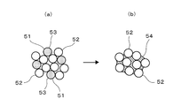
- a low melting point metal (for example, Sn) ball 51 and a high melting point metal (for example, Cu) ball 52 are schematically shown in FIG.
- the solder paste containing the flux 53 reacts by being heated, and after soldering, as shown in FIG. 2B, a plurality of high melting point metal balls 52 are low melting point derived from the low melting point metal balls. It is connected via an intermetallic compound 54 formed between a metal and a refractory metal derived from a refractory metal ball, and an object to be joined is connected and connected (soldered) by this linking body. become.
- an intermetallic compound of a high melting point metal (for example, Cu) and a low melting point metal (for example, Sn) is obtained by heating the solder paste in the soldering process.
- a high melting point metal for example, Cu
- Sn low melting point metal
- solder in the manufacturing process of the semiconductor device is used.
- Sn remaining in the attaching process may melt and flow out in the reflow soldering process.
- solder paste of Patent Document 1 for example, Cu 3 Sn or Cu 6 Sn is formed at the interface between the reflow target objects 61 and 62 and the bonding material (solder) 63 as shown in FIG.
- An intermetallic compound 64 such as 5 is formed in layers. When such a layered intermetallic compound 64 is formed, stress concentrates at the interface, so that the bonding strength at the interface decreases due to the occurrence of cracks and the like.
- the present invention solves the above-described problem, and can secure the sufficient joining strength while joining the first metal member and the second metal member, and a stage such as re-reflow in the temperature hierarchy connection. It is an object of the present invention to provide a bonding method, a bonding structure, an electronic device, a method for manufacturing an electronic device, and an electronic component capable of suppressing and preventing the flow of a bonding material in the case.
- the bonding method of the present invention is: A low melting point metal having a melting point lower than that of the first metal and / or the second metal between a first metal member having at least a surface made of the first metal and a second metal member having at least a surface made of the second metal.
- Placing a bonding material comprising: Heating the bonding material at a temperature equal to or higher than the melting point of the low melting point metal, In the step of heating the bonding material, an intermetallic compound is generated by a reaction between the low melting point metal and the first metal and / or the second metal, and the intermetallic compound is peeled in the molten low melting point metal. It is characterized by repeating the reaction while being dispersed.
- all the low melting point metals are intermetallic compounds in the step of heating the bonding material.
- the method of manufacturing the electronic component of the present invention includes A method for manufacturing an electronic device comprising: a first metal member having at least a surface made of a first metal; and a second metal member having at least a surface made of a second metal, It has the process of joining the said 1st metal member and the said 2nd metal member with the joining method of Claim 1 or 2. It is characterized by the above-mentioned.
- the joining method of the present invention comprises:
- the first metal member having at least the surface made of the first metal and the second metal member having at least the surface made of the second metal are mainly the low melting point metal having a melting point lower than that of the first metal and / or the second metal.
- a bonding method for bonding via a bonding material as a component The low melting point metal constituting the bonding material is Sn or an alloy containing 70% by weight or more of Sn, A metal or an alloy that forms an intermetallic compound between at least one of the first metal and the second metal and the low-melting-point metal constituting the bonding material, the first metal and the second metal A metal or alloy having a lattice constant difference of 50% or more with respect to an intermetallic compound formed on at least one surface of
- heat treatment is performed at a temperature at which the low melting point metal constituting the bonding material melts, and the first metal member and the second metal member It is characterized by comprising a heat treatment step for joining the metal member via the joining material.
- the low melting point metal is Sn or an alloy containing 85% by weight or more of Sn.
- the low melting point metal constituting the bonding material (a) the low melting point metal constituting the bonding material, and (b) the lattice constant difference between the first metal and the second metal is 50% or more. It is preferable to carry out the heat treatment step in a state in which the ratio of the latter to the total amount is 30% by volume or more.
- the low melting point metal constituting the bonding material is Sn alone or At least one selected from the group consisting of Cu, Ni, Ag, Au, Sb, Zn, Bi, In, Ge, Al, Co, Mn, Fe, Cr, Mg, Mn, Pd, Si, Sr, Te, and P And an alloy containing Sn.
- At least one of the first metal and the second metal is a Cu—Mn alloy or a Cu—Ni alloy.
- At least one of the first metal and the second metal is a Cu—Mn alloy containing Mn in a proportion of 5 to 30% by weight, or Cu—Ni containing Ni in a proportion of 5 to 30% by weight.
- An alloy is preferable, and in particular, a Cu—Mn alloy containing 10 to 15% by weight of Mn or a Cu—Ni alloy containing 10 to 15% by weight of Ni is preferable.
- the method of manufacturing the electronic component of the present invention includes A method for manufacturing an electronic device comprising: a first metal member having at least a surface made of a first metal; and a second metal member having at least a surface made of a second metal, A step of joining the first metal member and the second metal member by the joining method according to any one of claims 4 to 9 is provided.
- the bonding structure of the present invention is a bonding structure in which a first metal member and a second metal member are bonded via a bonding portion, and Cu—M—Sn (M Ni and / or Mn) intermetallic compounds are dispersed, and at least one of the interfaces between the first metal member and the second metal member has a Cu 3 Sn layer and a Cu 6 Sn layer as an intermetallic compound layer. It is characterized in that neither of the five layers is formed.
- the bonded structure of the present invention it is preferable that no intermetallic compound layer is formed in any of the interfaces between the first metal member and the second metal member in the bonded portion.
- the electronic device of the present invention is an electronic device in which a first metal member having at least a surface made of a first metal and a second metal member having at least a surface made of a second metal are joined via a joint portion. And the junction part of the said 1st metal member and the said 2nd metal member has the joining structure of Claim 11 or 12, It is characterized by the above-mentioned.
- the electronic component of the present invention is an electronic component including an electrode that is used for bonding with a bonding material containing a low-melting-point metal made of Sn or an alloy containing 70 wt% or more of Sn, and is in contact with the bonding material
- the surface of the electrode is a metal or alloy that forms an intermetallic compound with the low melting point metal, and the lattice constant difference between the electrode and the intermetallic compound formed on the surface of the electrode by reaction with the low melting point metal is It is characterized by being formed of a metal or alloy that is 50% or more.
- the surface of the electrode in contact with the bonding material is formed of a Cu—Mn alloy or a Cu—Ni alloy.
- the Cu—Mn alloy or the Cu—Ni alloy is a Cu—Mn alloy containing 5 to 30% by weight of Mn or a Cu—Ni alloy containing 5 to 30% by weight of Ni.
- a Cu—Mn alloy containing Mn in a proportion of 10 to 15% by weight or a Cu—Ni alloy containing Ni in a proportion of 10 to 15% by weight is more preferable.
- the joining method of the present invention has a melting point higher than that of the first metal and / or the second metal between the first metal member having at least the surface made of the first metal and the second metal member having at least the surface made of the second metal.
- a bonding material containing a low melting point metal having a low melting point and heating the bonding material at a temperature equal to or higher than the melting point of the low melting point metal.
- the low melting point metal and the first metal and / or Alternatively an intermetallic compound is generated by reaction with the second metal, and the reaction is repeated while the intermetallic compound is peeled and dispersed in the molten low melting point metal.
- the interdiffusion of the first metal and / or the second metal into the low melting point metal progresses dramatically, and the change to the higher melting point intermetallic compound is promoted. It becomes possible to perform joining with sufficient joining strength and impact resistance.
- step of heating the bonding material by making all the low melting point metals into intermetallic compounds, it is possible to perform bonding with higher heat resistance and sufficient bonding strength and impact resistance. Become.
- the manufacturing method of the electronic component of this invention is equipped with the process of joining the said 1st metal member and the said 2nd metal member by the joining method of Claim 1 or 2, it is the 1st metal member.
- a highly reliable electronic component in which the second metal member is reliably bonded through the bonding material can be efficiently manufactured.
- the first metal member having at least the surface made of the first metal and the second metal member having at least the surface made of the second metal have a melting point lower than that of the first metal and / or the second metal.
- the low melting point metal constituting the joining material is made of Sn or an alloy containing 70% by weight or more of at least one of the first metal and the second metal.
- a metal or an alloy that forms an intermetallic compound with a low-melting-point metal constituting the bonding material and has a lattice constant difference from the intermetallic compound formed on at least one surface of the first metal and the second metal. Since the metal or alloy is 50% or more, even when the joined body obtained by joining according to the method of the present invention is reflowed, the joining material is suppressed and prevented from remelting. , Bonding strength, it is possible to improve impact resistance.
- At least one of the first metal and the second metal is a metal or alloy that forms an intermetallic compound with a low melting point metal, and is at least one of the first metal and the second metal. Since a metal or an alloy having a lattice constant difference of 50% or more from the intermetallic compound formed on the surface of the metal is used, the mutual diffusion of the first metal and / or the second metal to the low melting point metal proceeds dramatically. In addition, since the change to an intermetallic compound having a higher melting point is promoted, it is possible to perform bonding with high heat resistance and sufficient bonding strength and impact resistance.
- the “lattice constant difference” is a value obtained by subtracting the lattice constant of the first metal or the second metal from the lattice constant of the intermetallic compound of the first metal or the second metal and the low melting point metal. , Defined as a numerical value (%) obtained by multiplying the absolute value of the numerical value divided by the lattice constant of the first metal or the second metal by 100.
- this difference in lattice constant indicates how much the lattice constant of the intermetallic compound newly generated at the interface with the first metal and / or the second metal is relative to the lattice constant of the first metal and / or the second metal. It indicates whether there is a difference, and it does not matter which lattice constant is large.
- the difference in lattice constant is expressed by the following formula (1).
- Lattice constant difference (%) ⁇ (lattice constant of intermetallic compound ⁇ lattice constant of first metal or second metal) / lattice constant of first metal or second metal ⁇ ⁇ 100 (1)
- the first metal member is heat-treated at a temperature at which the low melting point metal constituting the joining material is melted in a state where the joining material is disposed between the first metal member and the second metal member.
- the metal member and the second metal member are joined.
- the first metal and the second metal are metal materials constituting the first metal member (electrode main body) and the second metal member (electrode main body) to be bonded to each other, and at least one of them is the inter-metal A metal material having a lattice constant difference of 50% or more with respect to a compound, and a state in which a low melting point metal is supplied between the first metal member and the second metal member as a solder paste or a plate-like solder, 2)
- the first metal and the second metal are metal materials constituting a plating film formed on the surfaces of the first metal member (electrode body) and the second metal member (electrode body) to be joined to each other.
- the state currently supplied between the surfaces of the 2nd metal member is mentioned.
- the total amount of (a) the low melting point metal constituting the bonding material and (b) the first metal and the second metal having a lattice constant difference of 50% or more By carrying out the heat treatment step with the latter ratio being 30% by volume or more, the lattice constant difference between the first metal and the second metal is 50% or more, but the low melting point material constituting the bonding material is obtained. Is sufficiently progressed to promote the change to a higher melting point intermetallic compound, and the low melting point metal component hardly remains, so that it is possible to perform bonding with higher heat resistance strength.
- the state in which the ratio of the latter is 30% by volume or more means that, for example, when both the first metal and the second metal have the lattice constant difference of 50% or more, the following formula The state represented by (2). [(First metal + second metal) / ⁇ low melting point metal + (first metal + second metal) ⁇ ] ⁇ 100 ⁇ 30 (volume%) (2)
- the low melting point metal constituting the bonding material is Sn alone, or Cu, Ni, Ag, Au, Sb, Zn, Bi, In, Ge, Al, Co,
- the alloy includes Sn and at least one selected from the group consisting of Mn, Fe, Cr, Mg, Mn, Pd, Si, Sr, Te, and P
- the first difference in lattice constant is 50% or more. It becomes possible to easily form an intermetallic compound between at least one of the metal and the second metal.
- the first metal and the second metal is a Cu—Mn alloy or a Cu—Ni alloy
- an intermetallic compound with a low melting point metal can be generated at a lower temperature and in a shorter time. In the subsequent reflow process, it is possible not to melt.
- At least one of the first metal and the second metal is a Cu—Mn alloy containing Mn in a proportion of 3 to 30% by weight, in particular Cu—Mn containing Mn in a proportion of 10 to 15% by weight.
- the first metal member and the second metal member are The reliability that the first metal member and the second metal member are reliably bonded via the bonding material by bonding by the bonding method described above (the bonding method according to any one of claims 4 to 9).
- a highly efficient electronic device can be manufactured efficiently.
- At least a Cu-M-Sn (M is nickel and / or Mn) intermetallic compound is dispersed in the joining portion for joining the first metal member and the second metal member. Since the ratio of the unreacted Sn component that is not intermetallic compound to the entire bonding material is 30% by volume or less, the heat resistance strength is excellent, and the bonding material does not remelt and flow out in a process such as reflow. The bonding strength between the first metal member and the second metal member can be increased. Further, in the joint portion, a layered intermetallic compound (intermetallic compound layer) is not formed on at least one of the interfaces between the first metal member and the second metal member. Therefore, cracks and the like due to stress concentration such as thermal stress are unlikely to occur, the bonding strength between the first metal member and the second metal member against thermal shock can be increased, and a highly reliable bonding structure can be provided.
- M nickel and / or Mn
- neither the Cu 3 Sn layer or the Cu 6 Sn 5 layer which is an intermetallic compound layer is formed at any of the interfaces between the first metal member and the second metal member.
- the electronic device of the present invention is an electronic device in which a first metal member having at least a surface made of a first metal and a second metal member having at least a surface made of a second metal are joined via a joint portion. And since the junction part of a 1st metal member and a 2nd metal member is provided with the junction structure of Claim 11 or 12, the junction part of a 1st metal member and a 2nd metal member has high heat-resistant strength. An electronic component having sufficient bonding strength and impact resistance can be provided.
- the electronic component of the present invention is an electronic component including an electrode that is used for bonding with a bonding material containing a low-melting-point metal made of Sn or an alloy containing Sn by weight of 70% by weight or more.
- the surface is a metal or alloy that forms an intermetallic compound with a low melting point metal, and the difference in lattice constant from the intermetallic compound formed on the surface of the electrode by the reaction with the low melting point metal is 50% or more. Since it is formed of a certain metal or alloy, an electronic component suitable for use in the joining method of the present invention can be provided.
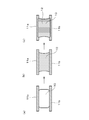
- FIG. It is a figure which shows typically the behavior in the case of joining to the joining method concerning the Example of this invention, (a) is a figure which shows the state before a heating, (b) is a heating start, and joining material melt
- FIG. It is a figure which shows the behavior of solder when soldering using the conventional solder paste, (a) is a figure which shows the state before heating, (b) is a figure which shows the state after the end of a soldering process. is there. It is a figure which shows the joining structure in which the layered intermetallic compound layer was formed in the interface at the time of joining using the conventional solder paste.
- a first metal member 11a made of a first metal and a second metal member 11b made of a second metal are combined with the first metal and the second metal. Bonding was performed using a bonding material 10 mainly composed of a low melting point metal having a melting point lower than that of the metal.
- the low melting point metal constituting the bonding material as shown in Table 1A and Table 1B, Sn-3Ag-0.5Cu, Sn, Sn-3.5Ag, Sn-0.75Cu, Sn— 0.7Cu-0.05Ni, Sn-5Sb, Sn-2Ag-0.5Cu-2Bi, Sn-57Bi-1Ag, Sn-3.5Ag-0.5Bi-8In, Sn-9Zn, Sn-8Zn-3Bi, Sn-10Bi, Sn-20Bi, Sn-30Bi, Sn-40Bi were used.
- Sn-3Ag-0.5Cu means that the low melting point metal material contains 3% by weight of Ag and 0.5% by weight of Cu. , The balance being Sn (Sn alloy). Therefore, among the above-mentioned low melting point materials, Sn-40Bi is a comparative example that does not satisfy the requirement of the present invention “Sn or an alloy containing 70 wt% or more of Sn”.
- Sn-40Bi is a comparative example that does not satisfy the requirement of the present invention “Sn or an alloy containing 70 wt% or more of Sn”.
- the first metal member and the second metal member as shown in Table 1A and Table 1B, Cu-10Ni, Cu-10Mn, Cu-12Mn-4Ni, Cu-10Mn-1P, Cu, Cu-10Zn are used. What was used.
- sample Nos. 16 and 17 in Table 1B different materials are used for the first metal material and the second metal material. That is, in sample number 16, Cu-10Ni is used for the first metal material (upper metal member) and Cu-10Mn is used in the second metal member (lower metal member). In sample number 17, the first metal member (upper metal) is used. Cu) was used for the member), and Cu-10Mn was used for the second metal member (lower metal member).
- the joining material formed into a plate shape is used as the first metal.
- the 1st metal member and the 2nd metal member were joined by arrange
- a bonding material 10 formed in a plate shape is positioned between the first metal member 11a and the second metal member 11b.
- the joined body by which the 1st metal member and the 2nd metal member were joined by the joining material containing the intermetallic compound solidified after reflow is obtained.
- the bonding method of the present invention it has been confirmed that Cu—M—Sn (M is nickel and / or Mn) intermetallic compounds are dispersed in the bonding material.
- ⁇ Residual component evaluation About 7 mg of a bonding material (reaction product) containing an intermetallic compound that has solidified after reflow is cut off and measured under the conditions of a measurement temperature of 30 ° C. to 300 ° C., a temperature increase rate of 5 ° C./min, an N 2 atmosphere, and a reference Al 2 O 3 . Differential scanning calorimetry (DSC measurement) was performed. From the endothermic amount of the melting endothermic peak at the melting temperature of the low melting point metal component of the obtained DSC chart, the amount of the remaining low melting point metal component was quantified to determine the residual low melting point metal content (volume%).
- DSC measurement Differential scanning calorimetry
- compositions of low melting point metals that make up the bonding material
- the composition of the metal (first metal and second metal) constituting the first metal member and the second metal member in sample numbers 1 to 15 in Table 1A and Table 1B, the first metal and the second metal are the same metal, the sample Nos. 16 and 17 are different metals) and their lattice constants
- the kind of intermetallic compound produced by the reaction between the low melting point metal constituting the bonding material and the first and / or second metal and its lattice constant (in this example, the lattice constant is evaluated based on the a-axis.
- a lattice constant difference that is a difference between the lattice constant of the intermetallic compound and the lattice constant of the first and / or second metal
- the first metal member and / or the second metal member made of a metal having a lattice constant difference of 50% or more in the joint is solidified after the reflow to join the first metal member and the second metal member.
- the presence or absence of a layered intermetallic compound of Cu 3 Sn and Cu 6 Sn 5 formed at the interface of the joint (joining material including the intermetallic compound) is also shown.
- the samples of the comparative examples of sample numbers 18 to 20 had insufficient bonding strength of 2 Nmm ⁇ 2 or less, whereas the samples of the examples of sample numbers 1 to 17 It has been confirmed that it has practical strength because it holds 10 Nmm -2 or more.
- the residual low melting point metal content in the case of the samples of the comparative examples of sample numbers 18 to 20, the residual low melting point metal content was larger than 30% by volume.
- the residual low melting point metal content can be reduced to 30% by volume or less, and in particular, a sample using an alloy containing Sn or Sn of 85% by weight or more as the low melting point metal.
- the residual low melting point metal content was 0% by volume.
- the flow-out failure rate of the bonding material was 70% or more in the case of the samples of the sample numbers 18 to 20, whereas the samples of the examples of the sample numbers 1 to 17 In the case of the samples of Examples Nos. 1 to 9 and 11 to 17 using the alloys containing 85% by weight or more of Sn or Sn as the low melting point metal, all of which have a flow-out defect rate of 20% or less. It was confirmed that the flow-out defect rate was as high as 0% and heat resistance.
- the samples of Examples Nos. 1 to 17 satisfying the requirements of the present invention include: As in the samples of sample numbers 1 to 16, the metals constituting the first metal member and the second metal member are the same metal and are based on Cu—Mn (Cu-12Mn-4Ni or Cu— 10Mn-1P etc.), A sample in which the first metal member and the second metal member are made of different metals, such as sample number 16, each of which has a lattice constant difference of 50% or more, ⁇ As in sample number 17, the first metal member and the second metal member are made of different metals, and one of them contains a sample whose lattice constant difference is less than 50%. Even in the case, it was confirmed that the heat resistance was similarly provided.
- the bonding strength after the thermal shock test is 5 Nmm ⁇ 2 (Sample No. 18).
- 7Nmm -2 (Sample No. 19) and 8Nmm -2 (Sample No. 20) were low, but the samples Nos. 1 to 17 satisfying the requirements of the present invention had comparative bonding strength after the thermal shock test. Compared to the case of, it was confirmed that the improvement was significant.
- the joint strength after the thermal shock test is 20 Nmm ⁇ 2 or more, the sample No. 10 (the Sn amount of the low melting point metal is 70% by weight) ), The bonding strength after thermal shock is 17 Nmm ⁇ 2 , the sample No. 17 (first metal member (upper metal member) is Cu, and second metal member (lower metal member) is Cu-10Mn. In a certain sample), the bonding strength after the thermal shock test was 15 Nmm ⁇ 2, which was lower than that of the samples Nos. 1 to 9 and 11 to 16, but it was confirmed that it was sufficiently practical.
- Cu constituting the first metal member has a lattice constant difference of less than 50% with respect to the upper intermetallic compound, but Cu— constituting the lower second metal member. Since 10Mn is a metal having a lattice constant difference of more than 50% from the intermetallic compound, the reaction with Sn or Sn alloy, which is a low melting point metal in the bonding material, is fast, so the Cu-10Mn side (second metal Side), the formation of intermetallic compounds becomes dominant, and even if Cu 3 Sn or Cu 6 Sn 5 layered intermetallic compounds are formed at the bonding interface on the Cu side (first metal side), the impact test is very thin. This is thought to be due to the fact that there was little influence on the subsequent bonding strength.
- a layered metal such as Cu 3 Sn or Cu 6 Sn 5 is provided at the interface with the second metal member made of a metal (Cu-10Mn) having a lattice constant difference exceeding 50% with respect to the intermetallic compound. It has been confirmed that no intermetallic compound is formed.
- the thermal shock is further applied to the joined body obtained after the reflow. It is considered that even when the test is performed, the intermetallic compound layer does not grow, cracks are not generated, and the bonding strength is maintained.
- the samples Nos. 1 to 17 satisfying the requirements of the present invention have high heat resistance because at least one of the first metal and the second metal constituting the first metal member and the second metal member.
- a Cu—Mn and Cu—Ni alloy having a lattice constant difference of 50% or more with respect to an intermetallic compound (Cu 2 MnSn and Cu 2 NiSn) formed between the low melting point metal constituting the bonding material. This is thought to be due to the use.
- the lattice constant difference between the generated intermetallic compound and the first metal and / or the second metal constituting the second metal member is large, the metal in the molten low melting point metal This is thought to be due to the fact that the intermetallic compound generation rate progresses dramatically because the intermetallic compound repeats the reaction while peeling and dispersing, and the layered intermetallic compound is not formed at the interface.
- the first metal member and the second metal member each made of Cu-10Mn were joined using a joining material in which Sn is a low melting point metal (samples 21 to 27 in Table 2).
- a first metal member and a second metal member each made of Cu-10Ni were joined using a joining material having Sn as a low melting point metal (samples 28 to 30 in Table 2).
- the thickness of the 1st metal member and the 2nd metal member was 0.1 mm.
- the bonding material as shown in Table 2, a plate-shaped bonding material having a thickness changed from 0.266 mm to 1.327 mm was used. Otherwise, the first metal member and the second metal member were joined under the same conditions as in Example 1 above.
- Example 2 the obtained bonded body was measured and evaluated in the same manner as in Example 1 above. Specifically, measurement of bonding strength, residual component evaluation, flow-out evaluation, presence of cracks after the thermal shock test, measurement of bonding strength, and the like were performed.
- the evaluation of the joint strength those having a shear strength of 20 Nmm ⁇ 2 or more are ⁇ (excellent), those having a shear strength of 2 Nmm ⁇ 2 or more and less than 20 Nmm ⁇ 2 are ⁇ (good), 2 Nmm ⁇ 2 or less. Were evaluated as x (impossible).
- ⁇ excellent in the case of 0 to 3% by volume
- ⁇ (good) in the case of exceeding 3% by volume and 30% by volume or less
- ⁇ in the case of greater than 30% by volume. (Not possible).
- 0 to 10% is ⁇ (excellent), more than 10%, 50% or less is ⁇ (good), and the case where it is larger than 50% is ⁇ (impossible). evaluated.
- Table 2 shows the bonding strength (room temperature, 260 ° C.), residual low melting point metal content, flow-out failure rate, presence or absence of cracking after the thermal shock test, and bonding strength of each bonded body.
- ratio (%)” in the column of “first and second metals” is the total thickness of the first metal member (Cu-10Mn) and the second metal member (Cu-10Mn) (sample)
- the ratio of the total thickness (0.2 mm) of the member (Cu-10Mn) and the second metal member (Cu-10Mn) is shown.
- each of the samples Nos. 21 to 30 has a bonding strength of 7 to 26 Nmm ⁇ 2 and 2 Nmm ⁇ 2 or more, so that practical bonding is performed. confirmed.
- the samples of Sample Nos. 21 to 23, 28, and 29 whose ratio is 30% by volume or more show a bonding strength of 23 Nmm ⁇ 2 or more and high heat resistance. It was confirmed that it had strength.
- the residual low melting point metal content is 30% by volume or less for each of the samples Nos. 21 to 30, and particularly the sample numbers 21 to 23 and Cu-10Ni in which the ratio of Cu-10Mn is 30% by volume or more.
- samples Nos. 28 and 29 having a ratio of 30% by volume or more it was confirmed that the residual low melting point metal content was 0% by volume.
- the flow-out defect rate of the bonding material is 50% or less for each of the samples Nos. 21 to 30, and particularly the proportion of the sample Nos. 21 to 23 and Cu-10Ni in which the ratio of Cu-10Mn is 30% by volume or more.
- the flow-out defect rate was 0%, and it was confirmed that high heat resistance was obtained.
- the first metal member and the second metal member made of metal (Cu—Mn alloy) as shown in sample numbers 31 to 35 in Table 3 were joined using a joining material having Sn as a low melting point metal. Also, the first metal member and the second metal member made of metal (Cu—Ni alloy) as shown in sample numbers 36 to 39 in Table 3 were joined using a joining material having Sn as a low melting point metal. .
- the thickness of the 1st metal member and the 2nd metal member was 0.3 mm. Further, as the bonding material, a plate-shaped bonding material having a thickness of 0.1 mm was used. Otherwise, the first metal member and the second metal member were joined under the same conditions as in Example 1 above.
- the obtained bonded body was subjected to characteristic measurement and evaluation in the same manner as in Example 1 above. Specifically, measurement of bonding strength, residual component evaluation, flow-out evaluation, presence of cracks after the thermal shock test, measurement of bonding strength, and the like were performed. In addition, in the evaluation of joining strength, the residual low melting point metal content rate, and the evaluation of the flow-out failure rate, the same evaluation as in Example 2 was performed.
- Table 3 shows the bonding strength (room temperature, 260 ° C.), residual low melting point metal content, flow-out defect rate, occurrence of cracks after the thermal shock test, and bonding strength of each bonded body.
- the bonding strength at room temperature was 20 Nmm ⁇ 2 or more for any of the sample numbers 31 to 39, and it was confirmed that the bonding strength was sufficient.
- the bonding strength in the 260 ° C. the sample of the sample No. 31-39 and 5 ⁇ 26Nmm -2, it was confirmed to have practical bonding strength 2Nmm -2 or more.
- first metal and the second metal are Cu-10Mn and the Cu-15Mn as in the samples of Sample Nos. 32 and 33, as in the samples of Sample Nos. 37 and 38, When the first metal and the second metal were Cu-10Ni and Cu-15Ni, it was confirmed that they exhibited a bonding strength of 24 Nmm ⁇ 2 or more and had high heat resistance.
- the residual low melting point metal content is 30% by volume or less for each of the samples 31 to 39, and the first metal and the second metal are Cu as in the samples 32 and 33.
- the first metal and the second metal are Cu-10Ni
- the case where it is Cu-15Ni as in the samples Nos. 37 and 38 It was confirmed that the residual low melting point metal content was 0% by volume.
- each of the samples Nos. 31 to 39 is 35% by volume or less, and the first metal and the second metal are more like the samples Nos. 32 and 33.
- the first metal and the second metal are Cu-10Ni, and when it is Cu-15Ni, as in the samples of Sample Nos. 37 and 38
- the flow-out defect rate was 0%, and it was confirmed that high heat resistance was obtained.
- a plate-shaped bonding material was used as the bonding material containing the low melting point metal.
- the flux and the low melting point metal (Sn-3Ag-0.5Cu powder) were used.
- the blended solder paste the first metal member made of Cu and the second metal member made of Cu-10Mn were joined.
- the above-mentioned solder paste is printed on the first metal member made of Cu, and the second metal member made of Cu-10Mn is superimposed thereon, and then reflowed at 250 ° C. for 30 minutes. By doing so, the 1st metal member and the 2nd metal member were joined.
- the obtained bonded body was subjected to characteristic measurement and evaluation in the same manner as in Example 1 above. Specifically, the properties were evaluated by measuring the bonding strength, residual component evaluation, flow out evaluation, the presence of cracks after the thermal shock test, and the bonding strength. As a result, it was confirmed that a joined body having the same characteristics as those of the samples of Examples 1 to 3 having the requirements of the present invention was obtained.
- the case where the entire first metal member is made of the first metal and the entire second metal member is made of the second metal has been described as an example.
- the metal and the second metal are metal materials constituting a plating film formed on the surfaces of the first metal member (electrode body) and the second metal member (electrode body) to be bonded to each other, at least one of which is It is also possible to adopt a configuration in which the metal material has a lattice constant difference of 50% or more from the intermetallic compound.
- Example 5 a solder paste containing a flux and a low melting point metal (Sn-3Ag-0.5Cu powder) was used, and a land electrode (first metal member in the present invention) made of Cu on a glass epoxy substrate, A chip capacitor (electronic component) and an external electrode (second metal member in the present invention) made of Cu-10Mn of a surface acoustic wave filter (SAW filter) (electronic component) are joined to a chip capacitor on a glass epoxy substrate. And an electronic device having a structure in which the surface acoustic wave filter is mounted. In other words, this electronic device is an electronic device having a structure in which the first metal member and the second metal member are bonded via a bonding material having the requirements of the present invention.
- SAW filter surface acoustic wave filter
- the above-described solder paste is printed on the first metal member made of Cu of the glass epoxy substrate, and the solder paste is printed thereon.
- the chip capacitor and SAW filter external electrode (second metal member) made of Cu-10Mn are overlaid, the first metal member and the second metal member are joined by reflowing at 250 ° C. for 30 minutes. did.
- the thickness of the 1st metal member was 0.05 mm
- the thickness of the 2nd metal member was 0.05 mm.
- the solder paste was printed on the land electrode using a metal mask having a thickness of 0.05 mm.
- Example 2 About the obtained joined body, it carried out similarly to the case of the said Example 1, and performed the characteristic measurement and evaluation. Specifically, the properties were evaluated by measuring the bonding strength, residual component evaluation, flow out evaluation, the presence of cracks after the thermal shock test, and the bonding strength. In addition, in the evaluation of the joining strength, the residual low melting point metal content rate, and the evaluation of the flow-out failure rate, the same criteria as in Example 2 were used. Table 4 shows the bonding strength (room temperature, 260 ° C.), residual low melting point metal content, flow-out failure rate, presence or absence of cracks after the thermal shock test, and bonding strength of each bonded body.
- the first metal and the second metal are metal materials constituting a plating film formed on the surfaces of the first metal member (electrode body) and the second metal member (electrode body) to be joined to each other, It is also possible to employ a configuration in which at least one of the above is a metal material having a lattice constant difference of 50% or more from the intermetallic compound.
- the present invention is not limited to the above-described embodiments.
- the type and composition of the low melting point metal constituting the bonding material, the first metal member having at least the surface made of the first metal, and the second metal having at least the surface made of the second metal can be made within the scope of the invention with respect to the types and compositions of the materials constituting the two metal members.
Abstract
Description
ところで、従来から広く用いられてきたSn-Pb系はんだにおいては、高温系はんだとして、例えばPbリッチのPb-5Sn(融点:314~310℃)、Pb-10Sn(融点:302~275℃)などを用いて330~350℃の温度ではんだ付けし、その後、例えば、低温系はんだのSn-37Pb共晶(183℃)などを用いて、上記の高温系はんだの融点以下の温度ではんだ付けすることにより、先のはんだ付けに用いた高温系はんだを溶融させることなく、はんだ付けによる接続を行う温度階層接続の方法が広く適用されている。 In mounting electronic components, a joining method using solder (solder paste) is widely used.
By the way, in the Sn—Pb solder that has been widely used conventionally, examples of the high temperature solder include Pb-rich Pb-5Sn (melting point: 314 to 310 ° C.), Pb-10 Sn (melting point: 302 to 275 ° C.), etc. And then soldering at a temperature below the melting point of the high temperature solder using, for example, Sn-37Pb eutectic (183 ° C.) of a low temperature solder. Therefore, a method of temperature hierarchical connection in which connection by soldering is performed without melting the high-temperature solder used for the previous soldering has been widely applied.
また、この特許文献1には、はんだペーストを用いた接合方法や、電子機器の製造方法が開示されている。 Examples of the solder paste used in this application include (a) a second metal (or alloy) ball made of a second metal such as Cu, Al, Au, Ag, or a high melting point alloy containing them, and (b) Sn or A solder paste containing a mixture of first metal balls made of In has been proposed (see Patent Document 1).
Patent Document 1 discloses a joining method using a solder paste and a method for manufacturing an electronic device.
少なくとも表面が第1金属からなる第1金属部材と、少なくとも表面が第2金属からなる第2金属部材との間に、前記第1金属および/または前記第2金属よりも融点の低い低融点金属を含む接合材料を配置する工程と、
前記低融点金属の融点以上の温度で前記接合材料を加熱する工程と
を備え、
前記接合材料を加熱する工程において、前記低融点金属と前記第1金属および/または前記第2金属との反応により金属間化合物が生成され、溶融した前記低融点金属中で前記金属間化合物が剥離、分散しながら反応を繰り返すこと
を特徴としている。 In order to solve the above problems, the bonding method of the present invention is:
A low melting point metal having a melting point lower than that of the first metal and / or the second metal between a first metal member having at least a surface made of the first metal and a second metal member having at least a surface made of the second metal. Placing a bonding material comprising:
Heating the bonding material at a temperature equal to or higher than the melting point of the low melting point metal,
In the step of heating the bonding material, an intermetallic compound is generated by a reaction between the low melting point metal and the first metal and / or the second metal, and the intermetallic compound is peeled in the molten low melting point metal. It is characterized by repeating the reaction while being dispersed.
少なくとも表面が第1金属からなる第1金属部材と、少なくとも表面が第2金属からなる第2金属部材とを備えた電子装置の製造方法であって、
前記第1金属部材と、前記第2金属部材とを、請求項1または2記載の接合方法により接合する工程を備えていることを特徴としている。 In addition, the method of manufacturing the electronic component of the present invention includes
A method for manufacturing an electronic device comprising: a first metal member having at least a surface made of a first metal; and a second metal member having at least a surface made of a second metal,
It has the process of joining the said 1st metal member and the said 2nd metal member with the joining method of Claim 1 or 2. It is characterized by the above-mentioned.
少なくとも表面が第1金属からなる第1金属部材と、少なくとも表面が第2金属からなる第2金属部材とを、前記第1金属および/または前記第2金属よりも融点の低い低融点金属を主たる成分とする接合材料を介して接合するための接合方法であって、
前記接合材料を構成する前記低融点金属を、SnまたはSnを70重量%以上含む合金とし、
前記第1金属および前記第2金属の少なくとも一方を、前記接合材料を構成する前記低融点金属との間に金属間化合物を生成する金属または合金であって、前記第1金属および前記第2金属の少なくとも一方の表面に生成する金属間化合物との格子定数差が50%以上である金属または合金とし、かつ、
前記第1金属部材と第2金属部材との間に前記接合材料を配置した状態で、前記接合材料を構成する前記低融点金属が溶融する温度で熱処理し、前記第1金属部材と前記第2金属部材とを前記接合材料を介して接合する熱処理工程を備えていること
を特徴としている。 Moreover, the joining method of the present invention comprises:
The first metal member having at least the surface made of the first metal and the second metal member having at least the surface made of the second metal are mainly the low melting point metal having a melting point lower than that of the first metal and / or the second metal. A bonding method for bonding via a bonding material as a component,
The low melting point metal constituting the bonding material is Sn or an alloy containing 70% by weight or more of Sn,
A metal or an alloy that forms an intermetallic compound between at least one of the first metal and the second metal and the low-melting-point metal constituting the bonding material, the first metal and the second metal A metal or alloy having a lattice constant difference of 50% or more with respect to an intermetallic compound formed on at least one surface of
In a state where the bonding material is disposed between the first metal member and the second metal member, heat treatment is performed at a temperature at which the low melting point metal constituting the bonding material melts, and the first metal member and the second metal member It is characterized by comprising a heat treatment step for joining the metal member via the joining material.
Sn単体、または、
Cu,Ni,Ag,Au,Sb,Zn,Bi,In,Ge,Al,Co,Mn,Fe,Cr,Mg,Mn,Pd,Si,Sr,Te,Pからなる群より選ばれる少なくとも1種と、Snとを含む合金
であることが好ましい。 In the bonding method of the present invention, the low melting point metal constituting the bonding material is
Sn alone or
At least one selected from the group consisting of Cu, Ni, Ag, Au, Sb, Zn, Bi, In, Ge, Al, Co, Mn, Fe, Cr, Mg, Mn, Pd, Si, Sr, Te, and P And an alloy containing Sn.
少なくとも表面が第1金属からなる第1金属部材と、少なくとも表面が第2金属からなる第2金属部材とを備えた電子装置の製造方法であって、
前記第1金属部材と、前記第2金属部材とを請求項4~9のいずれかに記載の接合方法により接合する工程を備えていること
を特徴としている。 In addition, the method of manufacturing the electronic component of the present invention includes
A method for manufacturing an electronic device comprising: a first metal member having at least a surface made of a first metal; and a second metal member having at least a surface made of a second metal,
A step of joining the first metal member and the second metal member by the joining method according to any one of claims 4 to 9 is provided.
特に、Cu-Mn合金またはCu-Ni合金は、Mnを5~30重量%の割合で含有するCu-Mn合金、または、Niを5~30重量%の割合で含有するCu-Ni合金であることが好ましく、さらに好ましくは、Mnを10~15重量%の割合で含有するCu-Mn合金、または、Niを10~15重量%の割合で含有するCu-Ni合金である。 In the electronic component of the present invention, it is preferable that the surface of the electrode in contact with the bonding material is formed of a Cu—Mn alloy or a Cu—Ni alloy.
In particular, the Cu—Mn alloy or the Cu—Ni alloy is a Cu—Mn alloy containing 5 to 30% by weight of Mn or a Cu—Ni alloy containing 5 to 30% by weight of Ni. A Cu—Mn alloy containing Mn in a proportion of 10 to 15% by weight or a Cu—Ni alloy containing Ni in a proportion of 10 to 15% by weight is more preferable.
なお、格子定数差は、下記の式(1)で表される。
格子定数差(%)={(金属間化合物の格子定数-第1金属または第2金属の格子定数)/第1金属または第2金属の格子定数}×100 ……(1) That is, this difference in lattice constant indicates how much the lattice constant of the intermetallic compound newly generated at the interface with the first metal and / or the second metal is relative to the lattice constant of the first metal and / or the second metal. It indicates whether there is a difference, and it does not matter which lattice constant is large.
The difference in lattice constant is expressed by the following formula (1).
Lattice constant difference (%) = {(lattice constant of intermetallic compound−lattice constant of first metal or second metal) / lattice constant of first metal or second metal} × 100 (1)
1)第1金属および第2金属が、互いに接合させるべき第1金属部材(電極本体)と第2金属部材(電極本体)を構成する金属材料であって、そのうちの少なくとも一方が、上記金属間化合物との格子定数差が50%以上である金属材料であり、低融点金属がソルダペーストや板状はんだなどとして、第1金属部材と第2金属部材の間に供給されている状態や、
2)第1金属および第2金属が、互いに接合させようとしている第1金属部材(電極本体)と第2金属部材(電極本体)の表面に形成されためっき膜を構成する金属材料であって、そのうちの少なくとも一方が、上記金属間化合物との格子定数差が50%以上である金属材料であり、低融点金属がソルダペーストや板状はんだなどとして、めっき膜を備えた第1金属部材と第2金属部材の表面間に供給されている状態
などが挙げられる。 In the joining method of the present invention, the first metal member is heat-treated at a temperature at which the low melting point metal constituting the joining material is melted in a state where the joining material is disposed between the first metal member and the second metal member. The metal member and the second metal member are joined. As a specific state in which such joining (heat treatment) is performed, for example,
1) The first metal and the second metal are metal materials constituting the first metal member (electrode main body) and the second metal member (electrode main body) to be bonded to each other, and at least one of them is the inter-metal A metal material having a lattice constant difference of 50% or more with respect to a compound, and a state in which a low melting point metal is supplied between the first metal member and the second metal member as a solder paste or a plate-like solder,
2) The first metal and the second metal are metal materials constituting a plating film formed on the surfaces of the first metal member (electrode body) and the second metal member (electrode body) to be joined to each other. , At least one of which is a metal material having a lattice constant difference of 50% or more from the intermetallic compound, the low melting point metal as a solder paste or a plate-like solder, and the first metal member provided with a plating film; The state currently supplied between the surfaces of the 2nd metal member is mentioned.
また、「……後者の割合が30体積%以上である状態」とは、例えば、第1金属および第2金属がいずれも、上記格子定数差が50%以上のものである場合、下記の式(2)で表される状態をいう。
[(第1金属+第2金属)/{低融点金属+(第1金属+第2金属)}]×100≧30(体積%)…… (2) In the bonding method of the present invention, the total amount of (a) the low melting point metal constituting the bonding material and (b) the first metal and the second metal having a lattice constant difference of 50% or more. By carrying out the heat treatment step with the latter ratio being 30% by volume or more, the lattice constant difference between the first metal and the second metal is 50% or more, but the low melting point material constituting the bonding material is obtained. Is sufficiently progressed to promote the change to a higher melting point intermetallic compound, and the low melting point metal component hardly remains, so that it is possible to perform bonding with higher heat resistance strength.
In addition, “... the state in which the ratio of the latter is 30% by volume or more” means that, for example, when both the first metal and the second metal have the lattice constant difference of 50% or more, the following formula The state represented by (2).
[(First metal + second metal) / {low melting point metal + (first metal + second metal)}] × 100 ≧ 30 (volume%) (2)
また、接合部中において、第1金属部材および第2金属部材との界面の少なくとも一方には、層状の金属間化合物(金属間化合物層)が形成されない。そのため、熱応力等の応力集中に起因するクラック等が発生しにくく、熱衝撃に対する第1金属部材と第2金属部材との接合強度を大きく、信頼性の高い接合構造を提供することができる。 In the joining structure of the present invention, at least a Cu-M-Sn (M is nickel and / or Mn) intermetallic compound is dispersed in the joining portion for joining the first metal member and the second metal member. Since the ratio of the unreacted Sn component that is not intermetallic compound to the entire bonding material is 30% by volume or less, the heat resistance strength is excellent, and the bonding material does not remelt and flow out in a process such as reflow. The bonding strength between the first metal member and the second metal member can be increased.
Further, in the joint portion, a layered intermetallic compound (intermetallic compound layer) is not formed on at least one of the interfaces between the first metal member and the second metal member. Therefore, cracks and the like due to stress concentration such as thermal stress are unlikely to occur, the bonding strength between the first metal member and the second metal member against thermal shock can be increased, and a highly reliable bonding structure can be provided.
また、第1金属部材および第2金属部材としては、表1A、表1Bに示すように、Cu-10Ni,Cu-10Mn,Cu-12Mn-4Ni,Cu-10Mn-1P,Cu,Cu-10Znからなるものを用いた。 In the description of the low melting point metal constituting the bonding material, for example, “Sn-3Ag-0.5Cu” means that the low melting point metal material contains 3% by weight of Ag and 0.5% by weight of Cu. , The balance being Sn (Sn alloy). Therefore, among the above-mentioned low melting point materials, Sn-40Bi is a comparative example that does not satisfy the requirement of the present invention “Sn or an alloy containing 70 wt% or more of Sn”.
As the first metal member and the second metal member, as shown in Table 1A and Table 1B, Cu-10Ni, Cu-10Mn, Cu-12Mn-4Ni, Cu-10Mn-1P, Cu, Cu-10Zn are used. What was used.
まず、図1(a)に示すように、第1金属部材11a、第2金属部材11bの間に板状に成形された接合材料10を位置させる。 Here, the joining method in this embodiment will be described with reference to FIGS. 1 (a) to 1 (c).
First, as shown in FIG. 1A, a
なお、本発明の接合方法によれば、接合材料中に、Cu-M-Sn(Mはニッケルおよび/またはMn)金属間化合物が分散して存在することが確認されている。 Thereby, the joined body by which the 1st metal member and the 2nd metal member were joined by the joining material containing the intermetallic compound solidified after reflow is obtained.
According to the bonding method of the present invention, it has been confirmed that Cu—M—Sn (M is nickel and / or Mn) intermetallic compounds are dispersed in the bonding material.
上述のようにして得た接合体を試料として、以下の方法で特性を測定し、評価した。 [Characteristic evaluation]
Using the joined body obtained as described above as a sample, the characteristics were measured and evaluated by the following methods.
接合強度については、得られた接合体のシアー強度を、ボンディングテスタを用いて測定し、評価した。
シアー強度の測定は、横押し速度:0.1mm・s-1、室温および260℃の条件下で行った。
そして、シアー強度が20Nmm-2以上のものを◎(優)、2Nmm-2以下のものを×(不可)と評価した。
表1A、表1Bに、各試料について調べた接合強度(室温、260℃)と評価結果を併せて示す。 ≪Joint strength≫
Regarding the bonding strength, the shear strength of the obtained bonded body was measured and evaluated using a bonding tester.
The shear strength was measured under the conditions of a lateral pressing speed: 0.1 mm · s −1 , room temperature, and 260 ° C.
Then, those shear strength of more than 20Nmm -2 ◎ (excellent), was evaluated as × (poor) those 2Nmm -2 or less.
Tables 1A and 1B also show the joint strength (room temperature, 260 ° C.) and the evaluation results examined for each sample.
リフロー後に凝固した、金属間化合物を含む接合材料(反応生成物)を約7mg切り取り、測定温度30℃~300℃、昇温速度5℃/min、N2雰囲気、リファレンスAl2O3の条件で示差走査熱量測定(DSC測定)を行った。得られたDSCチャートの低融点金属成分の溶融温度における溶融吸熱ピークの吸熱量から、残留した低融点金属成分量を定量化し、残留低融点金属含有率(体積%)を求めた。そして、残留低融点金属含有率が0~3体積%の場合を◎(優)、3体積%を超え、30体積%以下の場合を○(良)、30体積%より大きい場合を×(不可)と評価した。
表1A、表1Bに、残留低融点金属含有率と評価結果を併せて示す。 ≪Residual component evaluation≫
About 7 mg of a bonding material (reaction product) containing an intermetallic compound that has solidified after reflow is cut off and measured under the conditions of a measurement temperature of 30 ° C. to 300 ° C., a temperature increase rate of 5 ° C./min, an N 2 atmosphere, and a reference Al 2 O 3 . Differential scanning calorimetry (DSC measurement) was performed. From the endothermic amount of the melting endothermic peak at the melting temperature of the low melting point metal component of the obtained DSC chart, the amount of the remaining low melting point metal component was quantified to determine the residual low melting point metal content (volume%). When the residual low melting point metal content is 0 to 3% by volume, ◎ (excellent), when it exceeds 3% by volume and below 30% by volume, ○ (good), and when it is greater than 30% by volume, x ).
Tables 1A and 1B show the residual low melting point metal content and the evaluation results.
得られた接合体をエポキシ樹脂で封止して相対湿度85%の環境に放置し、ピーク温度260℃のリフロー条件で加熱して、接合材料が再溶融して流れ出す、流れ出し不良の発生割合を調べた。そして、その結果から流れ出し不良発生率を求め、評価した。
接合材料の流れ出し不良率が0~10%の場合を◎(優)、10%を超え、50%以下の場合は○(良)、50%より大きい場合を×(不可)と評価した。
表1A、表1Bに、流れ出し不良発生率と評価結果を併せて示す。 ≪Outflow defect rate≫
The obtained bonded body is sealed with an epoxy resin, left in an environment with a relative humidity of 85%, heated under reflow conditions at a peak temperature of 260 ° C., and the bonding material remelts and flows out. Examined. And the outflow defect incidence was calculated | required and evaluated from the result.
A case where the defective flow rate of the bonding material was 0 to 10% was evaluated as) (excellent), exceeding 10%, and when it was 50% or less, ○ (good), and a case where it was larger than 50% was evaluated as × (impossible).
In Table 1A and Table 1B, the outflow defect occurrence rate and the evaluation results are shown together.
得られた接合体(試料)を、-40℃/85℃のそれぞれの温度条件で各30分間保持するサイクルを1000回行った後の各試料について、クラック発生状態を観察した。そして、クラック発生の有無を評価した。 ≪Crack after thermal shock test, bonding strength≫
A crack generation state was observed for each sample after 1000 cycles of holding the obtained joined body (sample) for 30 minutes each at −40 ° C./85° C. respectively. And the presence or absence of crack generation was evaluated.
表1A,表1Bに、熱衝撃試験後のクラック有無,接合強度を併せて示す。なお、クラックの発生については、それ自体が問題というわけではなく、接合強度を低下させる要因となるために評価している。 Further, the bonding strength of each sample after the thermal shock test was evaluated in the same manner as described above. Then, those shear strength of more than 20Nmm -2 ◎ (Yu), 10Nmm -2 or more, the ○ (good) smaller than 20Nmm -2, were evaluated smaller than 10Nmm -2 × (the poor).
Tables 1A and 1B also show the presence or absence of cracks and the bonding strength after the thermal shock test. Note that the occurrence of cracks is not a problem in itself, but is evaluated because it causes a reduction in bonding strength.
・接合材料を構成する低融点金属の種類(組成)、
・第1金属部材と第2金属部材を構成する金属(第1金属および第2金属)の組成(表1A、表1Bの試料番号1~15では第1金属および第2金属は同一金属、試料番号16,17では異種金属)とその格子定数、
・接合材料を構成する低融点金属と、第1および/または第2金属の反応により生成する金属間化合物の種類とその格子定数(この実施例において、格子定数はa軸を基に評価している)、
・金属間化合物の格子定数と、第1および/または第2金属の格子定数の差である格子定数差、
・接合部中における、格子定数差が50%以上の金属からなる第1金属部材および/または第2金属部材と、リフロー後に凝固して、第1金属部材と第2金属部材を接合している接合部(金属間化合物を含む接合材料)の界面に形成されるCu3SnおよびCu6Sn5の層状の金属間化合物の有無
を併せて示す。 In Table 1A and Table 1B,
・ Types (compositions) of low melting point metals that make up the bonding material,
The composition of the metal (first metal and second metal) constituting the first metal member and the second metal member (in sample numbers 1 to 15 in Table 1A and Table 1B, the first metal and the second metal are the same metal, the sample Nos. 16 and 17 are different metals) and their lattice constants,
The kind of intermetallic compound produced by the reaction between the low melting point metal constituting the bonding material and the first and / or second metal and its lattice constant (in this example, the lattice constant is evaluated based on the a-axis. Is)
A lattice constant difference that is a difference between the lattice constant of the intermetallic compound and the lattice constant of the first and / or second metal,
The first metal member and / or the second metal member made of a metal having a lattice constant difference of 50% or more in the joint is solidified after the reflow to join the first metal member and the second metal member. The presence or absence of a layered intermetallic compound of Cu 3 Sn and Cu 6 Sn 5 formed at the interface of the joint (joining material including the intermetallic compound) is also shown.


・試料番号1~16の試料のように、第1金属部材および第2金属部材を構成する金属が互いに同一金属であって、Cu-Mnをベースとする金属(Cu-12Mn-4NiやCu-10Mn-1Pなど)である試料、
・試料番号16のように、第1金属部材と第2金属部材が異なる金属からなり、そのいずれものが上述の格子定数差が50%以上のものである試料、
・試料番号17のように、第1金属部材と第2金属部材が異なる金属からなり、その一方が、上述の格子定数差が50%未満である試料
が含まれているが、それらのいずれの場合にも、同様に高耐熱性を備えていることが確認された。 In addition, the samples of Examples Nos. 1 to 17 satisfying the requirements of the present invention include:
As in the samples of sample numbers 1 to 16, the metals constituting the first metal member and the second metal member are the same metal and are based on Cu—Mn (Cu-12Mn-4Ni or Cu— 10Mn-1P etc.),
A sample in which the first metal member and the second metal member are made of different metals, such as sample number 16, each of which has a lattice constant difference of 50% or more,
・ As in sample number 17, the first metal member and the second metal member are made of different metals, and one of them contains a sample whose lattice constant difference is less than 50%. Even in the case, it was confirmed that the heat resistance was similarly provided.
また、試料番号18の実施例の試料では、第1金属としてCuを用いたため、接合材料と第1金属との界面に層状の金属間化合物が形成された。その結果、接合材料と第1金属との界面にのみクラックが発生し、接合強度がやや低下した。 On the other hand, the occurrence of cracks as described above was not observed in the samples of Examples Nos. 1 to 9 and 11 to 16. On the other hand, in the sample of Example No. 10, since the Sn amount of the low melting point metal is 70% by weight, the first intermetallic compound produced was Cu 2 MnSn, but its diffusion rate was slow. Therefore, an intermetallic compound such as Cu 6 Sn 5 or Cu 3 Sn is segregated at a part of the interface at the interface between the bonding material and the first and / or second metal member, although it is not layered. As a result, after the thermal shock, a minute crack was generated at the interface, and the bonding strength was slightly reduced.
Further, in the sample of the example of sample number 18, since Cu was used as the first metal, a layered intermetallic compound was formed at the interface between the bonding material and the first metal. As a result, cracks occurred only at the interface between the bonding material and the first metal, and the bonding strength slightly decreased.
なお、接合部には、金属間化合物との格子定数差が50%を超える金属(Cu-10Mn)からなる第2金属部材との界面には、Cu3SnやCu6Sn5の層状の金属間化合物が形成されないことが確認されている。 In the case of the sample of sample number 17, Cu constituting the first metal member has a lattice constant difference of less than 50% with respect to the upper intermetallic compound, but Cu— constituting the lower second metal member. Since 10Mn is a metal having a lattice constant difference of more than 50% from the intermetallic compound, the reaction with Sn or Sn alloy, which is a low melting point metal in the bonding material, is fast, so the Cu-10Mn side (second metal Side), the formation of intermetallic compounds becomes dominant, and even if Cu 3 Sn or Cu 6 Sn 5 layered intermetallic compounds are formed at the bonding interface on the Cu side (first metal side), the impact test is very thin. This is thought to be due to the fact that there was little influence on the subsequent bonding strength.
It should be noted that a layered metal such as Cu 3 Sn or Cu 6 Sn 5 is provided at the interface with the second metal member made of a metal (Cu-10Mn) having a lattice constant difference exceeding 50% with respect to the intermetallic compound. It has been confirmed that no intermetallic compound is formed.
同じく、Snを低融点金属とする接合材料を用い、それぞれCu-10Niからなる第1金属部材および第2金属部材を接合した(表2の試料番号28~30の試料)。 The first metal member and the second metal member each made of Cu-10Mn were joined using a joining material in which Sn is a low melting point metal (samples 21 to 27 in Table 2).
Similarly, a first metal member and a second metal member each made of Cu-10Ni were joined using a joining material having Sn as a low melting point metal (samples 28 to 30 in Table 2).
また、接合材料としては、表2に示すように、厚さを0.266mmから1.327mmまで変化させた板状の接合材料を用いた。
その他は上記実施例1の場合と同様の条件で第1金属部材および第2金属部材の接合を行った。 In addition, the thickness of the 1st metal member and the 2nd metal member was 0.1 mm.
As the bonding material, as shown in Table 2, a plate-shaped bonding material having a thickness changed from 0.266 mm to 1.327 mm was used.
Otherwise, the first metal member and the second metal member were joined under the same conditions as in Example 1 above.
なお、この実施例2では、接合強度の評価にあたって、シアー強度が20Nmm-2以上のものを◎(優)、2Nmm-2以上で20Nmm-2未満のものを○(良)、2Nmm-2以下のものを×(不可)と評価した。
また、残留第1金属成分率については、0~3体積%の場合を◎(優)、3体積%を超え、30体積%以下の場合を○(良)、30体積%より大きい場合を×(不可)と評価した。 Then, the obtained bonded body was measured and evaluated in the same manner as in Example 1 above. Specifically, measurement of bonding strength, residual component evaluation, flow-out evaluation, presence of cracks after the thermal shock test, measurement of bonding strength, and the like were performed.
In this Example 2, in the evaluation of the joint strength, those having a shear strength of 20 Nmm −2 or more are ◎ (excellent), those having a shear strength of 2 Nmm −2 or more and less than 20 Nmm −2 are ○ (good), 2 Nmm −2 or less. Were evaluated as x (impossible).
As for the residual first metal component ratio, ◎ (excellent) in the case of 0 to 3% by volume, ○ (good) in the case of exceeding 3% by volume and 30% by volume or less, and × in the case of greater than 30% by volume. (Not possible).
表2に、各接合体の接合強度(室温、260℃)、残留低融点金属含有率、流れ出し不良率、熱衝撃試験後のクラック発生の有無および接合強度を表2に示す。 Moreover, about the presence or absence of the crack after a thermal shock test, the presence or absence of the generation of a crack was evaluated.
Table 2 shows the bonding strength (room temperature, 260 ° C.), residual low melting point metal content, flow-out failure rate, presence or absence of cracking after the thermal shock test, and bonding strength of each bonded body.

また、表3の試料番号36~39に示すような金属(Cu-Ni系合金)からなる第1金属部材と第2金属部材とを、Snを低融点金属とする接合材料を用いて接合した。 The first metal member and the second metal member made of metal (Cu—Mn alloy) as shown in sample numbers 31 to 35 in Table 3 were joined using a joining material having Sn as a low melting point metal.
Also, the first metal member and the second metal member made of metal (Cu—Ni alloy) as shown in sample numbers 36 to 39 in Table 3 were joined using a joining material having Sn as a low melting point metal. .
また、接合材料としては、厚さを0.1mmの板状の接合材料を用いた。
その他は上記実施例1の場合と同様の条件で第1金属部材および第2金属部材の接合を行った。 In addition, the thickness of the 1st metal member and the 2nd metal member was 0.3 mm.
Further, as the bonding material, a plate-shaped bonding material having a thickness of 0.1 mm was used.
Otherwise, the first metal member and the second metal member were joined under the same conditions as in Example 1 above.
なお、接合強度の評価および、残留低融点金属含有率の評価、流れ出し不良率の評価にあたっては、実施例2の場合と同様の基準で評価した。 Then, the obtained bonded body was subjected to characteristic measurement and evaluation in the same manner as in Example 1 above. Specifically, measurement of bonding strength, residual component evaluation, flow-out evaluation, presence of cracks after the thermal shock test, measurement of bonding strength, and the like were performed.
In addition, in the evaluation of joining strength, the residual low melting point metal content rate, and the evaluation of the flow-out failure rate, the same evaluation as in Example 2 was performed.

接合するにあたっては、Cuからなる第1金属部材上に、上述のソルダペーストを印刷し、その上にCu-10Mnからなる第2金属部材を重ね合わせた後、250℃、30分の条件でリフローすることにより、第1金属部材と第2金属部材とを接合した。 In the above Examples 1 to 3, a plate-shaped bonding material was used as the bonding material containing the low melting point metal. However, in this Example 4, the flux and the low melting point metal (Sn-3Ag-0.5Cu powder) were used. Using the blended solder paste, the first metal member made of Cu and the second metal member made of Cu-10Mn were joined.
In joining, the above-mentioned solder paste is printed on the first metal member made of Cu, and the second metal member made of Cu-10Mn is superimposed thereon, and then reflowed at 250 ° C. for 30 minutes. By doing so, the 1st metal member and the 2nd metal member were joined.
その結果、上記実施例1~3の本発明の要件を備えた各試料の場合と同等の特性を備えた接合体が得られることが確認された。 Then, the obtained bonded body was subjected to characteristic measurement and evaluation in the same manner as in Example 1 above. Specifically, the properties were evaluated by measuring the bonding strength, residual component evaluation, flow out evaluation, the presence of cracks after the thermal shock test, and the bonding strength.
As a result, it was confirmed that a joined body having the same characteristics as those of the samples of Examples 1 to 3 having the requirements of the present invention was obtained.
すなわち、この電子装置は、上記第1金属部材と、上記第2金属部材とが、本発明の要件を備えた接合材料を介して接合された構造を有する電子装置である。 In Example 5, a solder paste containing a flux and a low melting point metal (Sn-3Ag-0.5Cu powder) was used, and a land electrode (first metal member in the present invention) made of Cu on a glass epoxy substrate, A chip capacitor (electronic component) and an external electrode (second metal member in the present invention) made of Cu-10Mn of a surface acoustic wave filter (SAW filter) (electronic component) are joined to a chip capacitor on a glass epoxy substrate. And an electronic device having a structure in which the surface acoustic wave filter is mounted.
In other words, this electronic device is an electronic device having a structure in which the first metal member and the second metal member are bonded via a bonding material having the requirements of the present invention.
また、ソルダペーストは、厚さ0.05mmのメタルマスクを用いて上記ランド電極上に印刷した。 In addition, the thickness of the 1st metal member was 0.05 mm, and the thickness of the 2nd metal member was 0.05 mm.
The solder paste was printed on the land electrode using a metal mask having a thickness of 0.05 mm.
なお、接合強度の評価および、残留低融点金属含有率の評価、流れ出し不良率の評価にあたっては、上記実施例2の場合と同様の基準で評価した。
表4に、各接合体の接合強度(室温、260℃)、残留低融点金属含有率、流れ出し不良率、熱衝撃試験後のクラック発生の有無および接合強度を示す。 About the obtained joined body, it carried out similarly to the case of the said Example 1, and performed the characteristic measurement and evaluation. Specifically, the properties were evaluated by measuring the bonding strength, residual component evaluation, flow out evaluation, the presence of cracks after the thermal shock test, and the bonding strength.
In addition, in the evaluation of the joining strength, the residual low melting point metal content rate, and the evaluation of the flow-out failure rate, the same criteria as in Example 2 were used.
Table 4 shows the bonding strength (room temperature, 260 ° C.), residual low melting point metal content, flow-out failure rate, presence or absence of cracks after the thermal shock test, and bonding strength of each bonded body.

11a 第1金属部材(第1金属)
11b 第2金属部材(第2金属)
12 金属間化合物
64 層状の金属間化合物 10 Plate-
11b Second metal member (second metal)
12
Claims (18)
- 少なくとも表面が第1金属からなる第1金属部材と、少なくとも表面が第2金属からなる第2金属部材との間に、前記第1金属および/または前記第2金属よりも融点の低い低融点金属を含む接合材料を配置する工程と、
前記低融点金属の融点以上の温度で前記接合材料を加熱する工程と
を備え、
前記接合材料を加熱する工程において、前記低融点金属と前記第1金属および/または前記第2金属との反応により金属間化合物が生成され、溶融した前記低融点金属中で前記金属間化合物が剥離、分散しながら反応を繰り返すこと
を特徴とする接合方法。 A low melting point metal having a melting point lower than that of the first metal and / or the second metal between a first metal member having at least a surface made of the first metal and a second metal member having at least a surface made of the second metal. Placing a bonding material comprising:
Heating the bonding material at a temperature equal to or higher than the melting point of the low melting point metal;
With
In the step of heating the bonding material, an intermetallic compound is generated by a reaction between the low melting point metal and the first metal and / or the second metal, and the intermetallic compound is peeled in the molten low melting point metal. A joining method characterized by repeating the reaction while dispersing. - 前記接合材料を加熱する工程において、前記低融点金属をすべて金属間化合物とすることを特徴とする請求項1記載の接合方法。 The bonding method according to claim 1, wherein in the step of heating the bonding material, all of the low melting point metals are intermetallic compounds.
- 少なくとも表面が第1金属からなる第1金属部材と、少なくとも表面が第2金属からなる第2金属部材とを備えた電子装置の製造方法であって、
前記第1金属部材と、前記第2金属部材とを、請求項1または2記載の接合方法により接合する工程を備えていること
を特徴とする電子装置の製造方法。 A method for manufacturing an electronic device comprising: a first metal member having at least a surface made of a first metal; and a second metal member having at least a surface made of a second metal,
A method for manufacturing an electronic device, comprising: a step of bonding the first metal member and the second metal member by the bonding method according to claim 1. - 少なくとも表面が第1金属からなる第1金属部材と、少なくとも表面が第2金属からなる第2金属部材とを、前記第1金属および/または前記第2金属よりも融点の低い低融点金属を主たる成分とする接合材料を介して接合するための接合方法であって、
前記接合材料を構成する前記低融点金属を、SnまたはSnを70重量%以上含む合金とし、
前記第1金属および前記第2金属の少なくとも一方を、前記接合材料を構成する前記低融点金属との間に金属間化合物を生成する金属または合金であって、前記第1金属および前記第2金属の少なくとも一方の表面に生成する金属間化合物との格子定数差が50%以上である金属または合金とし、かつ、
前記第1金属部材と第2金属部材との間に前記接合材料を配置した状態で、前記接合材料を構成する前記低融点金属が溶融する温度で熱処理し、前記第1金属部材と前記第2金属部材とを前記接合材料を介して接合する熱処理工程を備えていること
を特徴とする接合方法。 The first metal member having at least the surface made of the first metal and the second metal member having at least the surface made of the second metal are mainly the low melting point metal having a melting point lower than that of the first metal and / or the second metal. A bonding method for bonding via a bonding material as a component,
The low melting point metal constituting the bonding material is Sn or an alloy containing 70% by weight or more of Sn,
A metal or an alloy that forms an intermetallic compound between at least one of the first metal and the second metal and the low-melting-point metal constituting the bonding material, the first metal and the second metal A metal or alloy having a lattice constant difference of 50% or more with respect to an intermetallic compound formed on at least one surface of
In a state where the bonding material is disposed between the first metal member and the second metal member, heat treatment is performed at a temperature at which the low melting point metal constituting the bonding material melts, and the first metal member and the second metal member A joining method, comprising: a heat treatment step for joining a metal member through the joining material. - 前記低融点金属はSnまたはSnを85重量%以上含む合金であることを特徴とする請求項4記載の接合方法。 5. The joining method according to claim 4, wherein the low melting point metal is Sn or an alloy containing 85% by weight or more of Sn.
- (a)前記接合材料を構成する前記低融点金属と、(b)前記第1金属および前記第2金属のうちの前記格子定数差が50%以上のものとの合計量に対する、後者の割合が30体積%以上の状態で、前記熱処理工程を実施することを特徴とする請求項4または5記載の接合方法。 The ratio of the latter to the total amount of (a) the low melting point metal constituting the bonding material, and (b) the first metal and the second metal having the lattice constant difference of 50% or more is The joining method according to claim 4 or 5, wherein the heat treatment step is performed in a state of 30% by volume or more.
- 前記接合材料を構成する前記低融点金属が、
Sn単体、または、
Cu、Ni、Ag、Au、Sb、Zn、Bi、In、Ge、Al、Co、Mn、Fe、Cr、Mg、Mn、Pd、Si、Sr、Te、Pからなる群より選ばれる少なくとも1種と、Snとを含む合金
であることを特徴とする請求項4~6のいずれかに記載の接合方法。 The low melting point metal constituting the bonding material is:
Sn alone or
At least one selected from the group consisting of Cu, Ni, Ag, Au, Sb, Zn, Bi, In, Ge, Al, Co, Mn, Fe, Cr, Mg, Mn, Pd, Si, Sr, Te, and P The bonding method according to any one of claims 4 to 6, wherein the bonding method is an alloy containing Sn and Sn. - 前記第1金属および前記第2金属の少なくとも一方が、Cu-Mn合金またはCu-Ni合金であることを特徴とする請求項4~7のいずれかに記載の接合方法。 8. The joining method according to claim 4, wherein at least one of the first metal and the second metal is a Cu—Mn alloy or a Cu—Ni alloy.
- 前記第1金属および前記第2金属の少なくとも一方が、
Mnを5~30重量%の割合で含有するCu-Mn合金、または、
Niを5~30重量%の割合で含有するCu-Ni合金
であることを特徴とする請求項8記載の接合方法。 At least one of the first metal and the second metal is
A Cu—Mn alloy containing 5 to 30% by weight of Mn, or
The joining method according to claim 8, wherein the joining method is a Cu-Ni alloy containing Ni in a proportion of 5 to 30% by weight. - 前記第1金属および前記第2金属の少なくとも一方が、
Mnを10~15重量%の割合で含有するCu-Mn合金、または、
Niを10~15重量%の割合で含有するCu-Ni合金
であることを特徴とする請求項8記載の接合方法。 At least one of the first metal and the second metal is
A Cu—Mn alloy containing Mn in a proportion of 10 to 15% by weight, or
The joining method according to claim 8, wherein the joining method is a Cu-Ni alloy containing Ni in a proportion of 10 to 15% by weight. - 少なくとも表面が第1金属からなる第1金属部材と、少なくとも表面が第2金属からなる第2金属部材とを備えた電子装置の製造方法であって、
前記第1金属部材と、前記第2金属部材とを請求項4~9のいずれかに記載の接合方法により接合する工程を備えていること
を特徴とする電子装置の製造方法。 A method for manufacturing an electronic device comprising: a first metal member having at least a surface made of a first metal; and a second metal member having at least a surface made of a second metal,
A method for manufacturing an electronic device, comprising the step of joining the first metal member and the second metal member by the joining method according to any one of claims 4 to 9. - 第1金属部材と、第2金属部材とが、接合部を介して接合された接合構造であって、前記接合部中には、少なくともCu-M-Sn(MはNiおよび/またはMn)金属間化合物が分散しており、前記第1金属部材および前記第2金属部材との界面の少なくとも一方には、金属間化合物層であるCu3Sn層およびCu6Sn5層のどちらもが形成されていないことを特徴とする接合構造。 A joining structure in which a first metal member and a second metal member are joined via a joining portion, and at least Cu-M-Sn (M is Ni and / or Mn) metal in the joining portion An intermetallic compound is dispersed, and at least one of the interface between the first metal member and the second metal member is formed with both a Cu 3 Sn layer and a Cu 6 Sn 5 layer which are intermetallic compound layers. Bonding structure characterized by not.
- 前記接合部中には、前記第1金属部材および前記第2金属部材との界面のいずれにも、金属間化合物層であるCu3Sn層およびCu6Sn5層のどちらもが形成されていないことを特徴とする、請求項12記載の接合構造。 In the joint, neither the Cu 3 Sn layer nor the Cu 6 Sn 5 layer, which is an intermetallic compound layer, is formed at any of the interfaces between the first metal member and the second metal member. The joining structure according to claim 12, wherein
- 少なくとも表面が第1金属からなる第1金属部材と、少なくとも表面が第2金属からなる第2金属部材とが、接合部を介して接合された電子装置であって、
前記第1金属部材と前記第2金属部材の接合部が、請求項12または13記載の接合構造を有していること
を特徴とする電子装置。 An electronic device in which at least a first metal member having a surface made of a first metal and a second metal member having at least a surface made of a second metal are joined via a joining portion,
The electronic device according to claim 12, wherein a joint portion between the first metal member and the second metal member has a joint structure according to claim 12. - SnまたはSnを70重量%以上含む合金からなる低融点金属を含む接合材料による接合に供される電極を備えた電子部品であって、
前記接合材料に接する前記電極の表面が、前記低融点金属との間に金属間化合物を生成する金属または合金であって、前記低融点金属との反応により前記電極の表面に生成する金属間化合物との格子定数差が50%以上である金属または合金によって形成されていること
を特徴とする電子部品。 An electronic component including an electrode to be used for bonding with a bonding material containing a low melting point metal made of Sn or an alloy containing 70 wt% or more of Sn,
The surface of the electrode in contact with the bonding material is a metal or an alloy that generates an intermetallic compound with the low melting point metal, and the intermetallic compound is generated on the surface of the electrode by reaction with the low melting point metal. An electronic component characterized by being made of a metal or alloy having a lattice constant difference of 50% or more. - 前記接合材料に接する前記電極の表面が、Cu-Mn合金またはCu-Ni合金によって形成されていることを特徴とする、請求項15記載の電子部品。 16. The electronic component according to claim 15, wherein the surface of the electrode in contact with the bonding material is formed of a Cu—Mn alloy or a Cu—Ni alloy.
- 前記接合材料に接する前記電極の表面が、
Mnを5~30重量%の割合で含有するCu-Mn合金、または、
Niを5~30重量%の割合で含有するCu-Ni合金によって形成されていること
を特徴とする、請求項16記載の電子部品。 The surface of the electrode in contact with the bonding material is
A Cu—Mn alloy containing 5 to 30% by weight of Mn, or
The electronic component according to claim 16, wherein the electronic component is made of a Cu-Ni alloy containing Ni in a proportion of 5 to 30 wt%. - 前記接合材料に接する前記電極の表面が、
Mnを10~15重量%の割合で含有するCu-Mn合金、または、
Niを10~15重量%の割合で含有するCu-Ni合金によって形成されていること
を特徴とする、請求項16記載の電子部品。 The surface of the electrode in contact with the bonding material is
A Cu—Mn alloy containing Mn in a proportion of 10 to 15% by weight, or
The electronic component according to claim 16, wherein the electronic component is made of a Cu-Ni alloy containing Ni in a proportion of 10 to 15 wt%.
Priority Applications (6)
| Application Number | Priority Date | Filing Date | Title |
|---|---|---|---|
| CN201180049028.9A CN103167926B (en) | 2010-12-24 | 2011-12-22 | Joint method, connected structure, electronic installation and manufacture method thereof, electronic unit |
| KR1020137007337A KR101528515B1 (en) | 2010-12-24 | 2011-12-22 | Bonding method, bonding structure, electronic device, manufacturing method for electronic device, and electronic component |
| JP2012549868A JP5664664B2 (en) | 2010-12-24 | 2011-12-22 | Bonding method, electronic device manufacturing method, and electronic component |
| EP11851801.8A EP2656955B1 (en) | 2010-12-24 | 2011-12-22 | Method of bonding, method of manufacturing of electronic device, bonding structure, electronic device with such bonding structure |
| US13/904,072 US9209527B2 (en) | 2010-12-24 | 2013-05-29 | Joining method, joint structure, electronic device, method for manufacturing electronic device and electronic part |
| US14/918,648 US9614295B2 (en) | 2010-12-24 | 2015-10-21 | Joining method, joint structure, electronic device, method for manufacturing electronic device and electronic part |
Applications Claiming Priority (4)
| Application Number | Priority Date | Filing Date | Title |
|---|---|---|---|
| JP2010287782 | 2010-12-24 | ||
| JP2010-287782 | 2010-12-24 | ||
| JP2011159922 | 2011-07-21 | ||
| JP2011-159922 | 2011-07-21 |
Related Child Applications (1)
| Application Number | Title | Priority Date | Filing Date |
|---|---|---|---|
| US13/904,072 Continuation US9209527B2 (en) | 2010-12-24 | 2013-05-29 | Joining method, joint structure, electronic device, method for manufacturing electronic device and electronic part |
Publications (1)
| Publication Number | Publication Date |
|---|---|
| WO2012086745A1 true WO2012086745A1 (en) | 2012-06-28 |
Family
ID=46314012
Family Applications (1)
| Application Number | Title | Priority Date | Filing Date |
|---|---|---|---|
| PCT/JP2011/079781 WO2012086745A1 (en) | 2010-12-24 | 2011-12-22 | Bonding method, bonding structure, electronic device, manufacturing method for electronic device, and electronic component |
Country Status (7)
| Country | Link |
|---|---|
| US (2) | US9209527B2 (en) |
| EP (1) | EP2656955B1 (en) |
| JP (2) | JP5664664B2 (en) |
| KR (1) | KR101528515B1 (en) |
| CN (1) | CN103167926B (en) |
| TW (1) | TWI461252B (en) |
| WO (1) | WO2012086745A1 (en) |
Cited By (5)
| Publication number | Priority date | Publication date | Assignee | Title |
|---|---|---|---|---|
| JP2016069231A (en) * | 2014-09-30 | 2016-05-09 | 株式会社村田製作所 | Manufacturing method of stained glass, metal paste for conjugating stained glass |
| WO2017134974A1 (en) * | 2016-02-01 | 2017-08-10 | 株式会社村田製作所 | Bonding material, and bonding method and bonding structure using same |
| CN108098172A (en) * | 2017-12-01 | 2018-06-01 | 北京工业大学 | It is a kind of realize Cu/Sn/Cu interfaces can reverse connection method |
| CN109570813A (en) * | 2017-09-29 | 2019-04-05 | 松下知识产权经营株式会社 | Solder alloy and the bonded structure for using it |
| WO2021045131A1 (en) * | 2019-09-02 | 2021-03-11 | 株式会社日本スペリア社 | Solder paste and solder bonded body |
Families Citing this family (17)
| Publication number | Priority date | Publication date | Assignee | Title |
|---|---|---|---|---|
| JP6011734B2 (en) * | 2014-01-07 | 2016-10-19 | 株式会社村田製作所 | Structural material joining method and joining structure |
| CN106233005B (en) * | 2014-04-18 | 2018-09-28 | 株式会社村田制作所 | Adherency separation method, the metallic composite of bur |
| CN105081500B (en) * | 2015-09-02 | 2017-02-22 | 哈尔滨工业大学 | Method for inducing growth of intermetallic compound with specific grain orientation and specific number of films through laser forward transfer printing |
| JP6332566B2 (en) | 2015-09-15 | 2018-05-30 | 株式会社村田製作所 | Joining member, method for producing joining member, and joining method |
| CN107850400B (en) | 2015-09-28 | 2019-10-25 | 株式会社村田制作所 | The manufacturing method of heat pipe, heat dissipation element, heat pipe |
| JP6369640B2 (en) * | 2015-11-05 | 2018-08-08 | 株式会社村田製作所 | Joining member and method for manufacturing joining member |
| JP6621068B2 (en) * | 2016-12-08 | 2019-12-18 | パナソニックIpマネジメント株式会社 | Mounting structure |
| JP6355091B1 (en) * | 2017-03-07 | 2018-07-11 | パナソニックIpマネジメント株式会社 | Solder alloy and joint structure using the same |
| CN109983544A (en) * | 2017-03-23 | 2019-07-05 | 积水化学工业株式会社 | Electroconductive particle, conductive material and connection structural bodies |
| DE102017206932A1 (en) * | 2017-04-25 | 2018-10-25 | Siemens Aktiengesellschaft | Lotformteil for producing a Diffusionslötverbindung and method for producing a Lotformteils |
| KR102574413B1 (en) * | 2018-12-10 | 2023-09-04 | 삼성전기주식회사 | Coil electronic component |
| US11581239B2 (en) * | 2019-01-18 | 2023-02-14 | Indium Corporation | Lead-free solder paste as thermal interface material |
| KR102148297B1 (en) * | 2019-03-06 | 2020-08-26 | 성균관대학교산학협력단 | Method for hybrid transient liquid phase sintering bonding for dissimilar material bonding |
| CN109822256B (en) * | 2019-03-15 | 2021-08-06 | 南昌大学 | Low-melting-point In-Sn-Bi alloy solder and preparation method thereof |
| JP6803107B1 (en) * | 2019-07-26 | 2020-12-23 | 株式会社日本スペリア社 | Preform solder and a solder joint formed by using the preform solder |
| CN113275787B (en) * | 2020-01-31 | 2023-05-30 | 铟泰公司 | Lead-free solder paste as thermal interface material |
| JP6799701B1 (en) * | 2020-03-12 | 2020-12-16 | 有限会社 ナプラ | Metal particles |
Citations (9)
| Publication number | Priority date | Publication date | Assignee | Title |
|---|---|---|---|---|
| JP2002254195A (en) * | 2000-12-25 | 2002-09-10 | Tdk Corp | Soldering composition and soldering method |
| JP2002254194A (en) | 2000-06-12 | 2002-09-10 | Hitachi Ltd | Electronic equipment |
| JP2003094193A (en) * | 2002-06-18 | 2003-04-02 | Matsushita Electric Ind Co Ltd | Lead-free solder paste |
| JP2003211289A (en) * | 2002-01-21 | 2003-07-29 | Fujitsu Ltd | Electrically conductive joining material, method of joining by using the same and electronic device |
| JP2003332731A (en) * | 2002-05-09 | 2003-11-21 | Murata Mfg Co Ltd | ARTICLE SOLDERED WITH Pb-FREE SOLDER |
| JP2005288458A (en) * | 2004-03-31 | 2005-10-20 | Toshiba Corp | Joined body, semiconductor device, joining method and method for producing semiconductor device |
| WO2006075459A1 (en) * | 2005-01-11 | 2006-07-20 | Murata Manufacturing Co., Ltd | Solder paste and electronic device |
| WO2007125861A1 (en) * | 2006-04-26 | 2007-11-08 | Senju Metal Industry Co., Ltd. | Solder paste |
| JP2010149185A (en) * | 2008-11-28 | 2010-07-08 | Asahi Kasei E-Materials Corp | Metal filler, solder paste and joint structure |
Family Cites Families (16)
| Publication number | Priority date | Publication date | Assignee | Title |
|---|---|---|---|---|
| US6371361B1 (en) * | 1996-02-09 | 2002-04-16 | Matsushita Electric Industrial Co., Ltd. | Soldering alloy, cream solder and soldering method |
| US5863493A (en) * | 1996-12-16 | 1999-01-26 | Ford Motor Company | Lead-free solder compositions |
| KR100377232B1 (en) * | 1998-03-26 | 2003-03-26 | 니혼 슈페리어 샤 가부시키 가이샤 | Leadless Solder |
| US6602777B1 (en) * | 2001-12-28 | 2003-08-05 | National Central University | Method for controlling the formation of intermetallic compounds in solder joints |
| WO2005041290A1 (en) * | 2003-10-24 | 2005-05-06 | Nikko Materials Co., Ltd. | Nickel alloy sputtering target and nickel alloy thin film |
| US7064446B2 (en) | 2004-03-29 | 2006-06-20 | Intel Corporation | Under bump metallization layer to enable use of high tin content solder bumps |
| JP4344707B2 (en) * | 2005-02-24 | 2009-10-14 | 株式会社ルネサステクノロジ | Semiconductor device and manufacturing method thereof |
| JP4501818B2 (en) * | 2005-09-02 | 2010-07-14 | 日立電線株式会社 | Copper alloy material and method for producing the same |
| WO2008026335A1 (en) | 2006-09-01 | 2008-03-06 | Murata Manufacturing Co., Ltd. | Electronic part device and method of manufacturing it and electronic part assembly and method of manufacturing it |
| EP2157605B1 (en) | 2007-06-04 | 2016-07-13 | Murata Manufacturing Co. Ltd. | Electronic part apparatus and process for manufacturing the same |
| KR101406174B1 (en) * | 2007-06-18 | 2014-06-12 | 엠케이전자 주식회사 | Lead free solder containing Sn, Ag and Bi |
| WO2009051181A1 (en) | 2007-10-19 | 2009-04-23 | Nihon Superior Sha Co., Ltd. | Lead-free solder alloy |
| JP4851596B2 (en) * | 2007-11-01 | 2012-01-11 | 古河電気工業株式会社 | Method for producing copper alloy material |
| JP5169354B2 (en) * | 2008-03-18 | 2013-03-27 | 富士通株式会社 | Joining material and joining method using the same |
| KR101276147B1 (en) * | 2009-09-03 | 2013-06-18 | 가부시키가이샤 무라타 세이사쿠쇼 | Soldering paste, bonding method using same, and bonding structure |
| WO2012066795A1 (en) * | 2010-11-19 | 2012-05-24 | 株式会社村田製作所 | Electroconductive material, method of connection with same, and connected structure |
-
2011
- 2011-12-21 TW TW100147807A patent/TWI461252B/en active
- 2011-12-22 EP EP11851801.8A patent/EP2656955B1/en active Active
- 2011-12-22 WO PCT/JP2011/079781 patent/WO2012086745A1/en active Application Filing
- 2011-12-22 KR KR1020137007337A patent/KR101528515B1/en active IP Right Grant
- 2011-12-22 JP JP2012549868A patent/JP5664664B2/en active Active
- 2011-12-22 CN CN201180049028.9A patent/CN103167926B/en active Active
-
2013
- 2013-05-29 US US13/904,072 patent/US9209527B2/en active Active
-
2014
- 2014-06-24 JP JP2014129244A patent/JP5907215B2/en active Active
-
2015
- 2015-10-21 US US14/918,648 patent/US9614295B2/en active Active
Patent Citations (9)
| Publication number | Priority date | Publication date | Assignee | Title |
|---|---|---|---|---|
| JP2002254194A (en) | 2000-06-12 | 2002-09-10 | Hitachi Ltd | Electronic equipment |
| JP2002254195A (en) * | 2000-12-25 | 2002-09-10 | Tdk Corp | Soldering composition and soldering method |
| JP2003211289A (en) * | 2002-01-21 | 2003-07-29 | Fujitsu Ltd | Electrically conductive joining material, method of joining by using the same and electronic device |
| JP2003332731A (en) * | 2002-05-09 | 2003-11-21 | Murata Mfg Co Ltd | ARTICLE SOLDERED WITH Pb-FREE SOLDER |
| JP2003094193A (en) * | 2002-06-18 | 2003-04-02 | Matsushita Electric Ind Co Ltd | Lead-free solder paste |
| JP2005288458A (en) * | 2004-03-31 | 2005-10-20 | Toshiba Corp | Joined body, semiconductor device, joining method and method for producing semiconductor device |
| WO2006075459A1 (en) * | 2005-01-11 | 2006-07-20 | Murata Manufacturing Co., Ltd | Solder paste and electronic device |
| WO2007125861A1 (en) * | 2006-04-26 | 2007-11-08 | Senju Metal Industry Co., Ltd. | Solder paste |
| JP2010149185A (en) * | 2008-11-28 | 2010-07-08 | Asahi Kasei E-Materials Corp | Metal filler, solder paste and joint structure |
Cited By (8)
| Publication number | Priority date | Publication date | Assignee | Title |
|---|---|---|---|---|
| JP2016069231A (en) * | 2014-09-30 | 2016-05-09 | 株式会社村田製作所 | Manufacturing method of stained glass, metal paste for conjugating stained glass |
| WO2017134974A1 (en) * | 2016-02-01 | 2017-08-10 | 株式会社村田製作所 | Bonding material, and bonding method and bonding structure using same |
| JPWO2017134974A1 (en) * | 2016-02-01 | 2018-10-04 | 株式会社村田製作所 | Bonding material, bonding method and bonding structure using the same |
| US10751841B2 (en) | 2016-02-01 | 2020-08-25 | Murata Manufacturing Co., Ltd. | Bonding material, and bonding method and bonded structure each using same |
| CN109570813A (en) * | 2017-09-29 | 2019-04-05 | 松下知识产权经营株式会社 | Solder alloy and the bonded structure for using it |
| CN109570813B (en) * | 2017-09-29 | 2021-07-16 | 松下知识产权经营株式会社 | Solder alloy and bonded structure using same |
| CN108098172A (en) * | 2017-12-01 | 2018-06-01 | 北京工业大学 | It is a kind of realize Cu/Sn/Cu interfaces can reverse connection method |
| WO2021045131A1 (en) * | 2019-09-02 | 2021-03-11 | 株式会社日本スペリア社 | Solder paste and solder bonded body |
Also Published As
| Publication number | Publication date |
|---|---|
| US9209527B2 (en) | 2015-12-08 |
| EP2656955A1 (en) | 2013-10-30 |
| EP2656955A4 (en) | 2017-07-19 |
| JP5664664B2 (en) | 2015-02-04 |
| US20160043480A1 (en) | 2016-02-11 |
| TW201233485A (en) | 2012-08-16 |
| JP5907215B2 (en) | 2016-04-26 |
| KR101528515B1 (en) | 2015-06-12 |
| EP2656955B1 (en) | 2021-08-04 |
| JP2014223678A (en) | 2014-12-04 |
| US9614295B2 (en) | 2017-04-04 |
| CN103167926A (en) | 2013-06-19 |
| US20130299236A1 (en) | 2013-11-14 |
| KR20130077873A (en) | 2013-07-09 |
| TWI461252B (en) | 2014-11-21 |
| JPWO2012086745A1 (en) | 2014-06-05 |
| CN103167926B (en) | 2016-03-09 |
Similar Documents
| Publication | Publication Date | Title |
|---|---|---|
| JP5907215B2 (en) | Junction structure and electronic device | |
| JP7135171B2 (en) | solder composition | |
| JP2014223678A5 (en) | ||
| JP5943065B2 (en) | Bonding method, electronic device manufacturing method, and electronic component | |
| JP5045673B2 (en) | Functional component lid and manufacturing method thereof | |
| TWI505899B (en) | A bonding method, a bonding structure, and a method for manufacturing the same | |
| JP5142999B2 (en) | Cream solder and soldering method for electronic parts | |
| JP5938032B2 (en) | Mixed alloy solder paste | |
| WO2013132942A1 (en) | Bonding method, bond structure, and manufacturing method for same | |
| TWI681063B (en) | Mixed alloy solder paste | |
| WO2011027820A1 (en) | Lead-free solder alloy, joining member and manufacturing method thereof, and electronic component | |
| KR101360142B1 (en) | Lead-free solder composition | |
| JP2023524690A (en) | Lead-free solder paste for high temperature applications with mixed solder powders | |
| WO2016157971A1 (en) | Solder paste | |
| JP2017148862A (en) | Solder Paste |
Legal Events
| Date | Code | Title | Description |
|---|---|---|---|
| WWE | Wipo information: entry into national phase |
Ref document number: 201180049028.9 Country of ref document: CN |
|
| 121 | Ep: the epo has been informed by wipo that ep was designated in this application |
Ref document number: 11851801 Country of ref document: EP Kind code of ref document: A1 |
|
| ENP | Entry into the national phase |
Ref document number: 20137007337 Country of ref document: KR Kind code of ref document: A |
|
| WWE | Wipo information: entry into national phase |
Ref document number: 2011851801 Country of ref document: EP |
|
| ENP | Entry into the national phase |
Ref document number: 2012549868 Country of ref document: JP Kind code of ref document: A |
|
| NENP | Non-entry into the national phase |
Ref country code: DE |