WO2012086503A1 - 液晶表示装置及び液晶表示装置の駆動方法 - Google Patents
液晶表示装置及び液晶表示装置の駆動方法 Download PDFInfo
- Publication number
- WO2012086503A1 WO2012086503A1 PCT/JP2011/078995 JP2011078995W WO2012086503A1 WO 2012086503 A1 WO2012086503 A1 WO 2012086503A1 JP 2011078995 W JP2011078995 W JP 2011078995W WO 2012086503 A1 WO2012086503 A1 WO 2012086503A1
- Authority
- WO
- WIPO (PCT)
- Prior art keywords
- liquid crystal
- electrode
- substrate
- display device
- crystal display
- Prior art date
- Legal status (The legal status is an assumption and is not a legal conclusion. Google has not performed a legal analysis and makes no representation as to the accuracy of the status listed.)
- Ceased
Links
Images




Classifications
-
- H—ELECTRICITY
- H04—ELECTRIC COMMUNICATION TECHNIQUE
- H04N—PICTORIAL COMMUNICATION, e.g. TELEVISION
- H04N13/00—Stereoscopic video systems; Multi-view video systems; Details thereof
- H04N13/30—Image reproducers
- H04N13/349—Multi-view displays for displaying three or more geometrical viewpoints without viewer tracking
-
- G—PHYSICS
- G02—OPTICS
- G02F—OPTICAL DEVICES OR ARRANGEMENTS FOR THE CONTROL OF LIGHT BY MODIFICATION OF THE OPTICAL PROPERTIES OF THE MEDIA OF THE ELEMENTS INVOLVED THEREIN; NON-LINEAR OPTICS; FREQUENCY-CHANGING OF LIGHT; OPTICAL LOGIC ELEMENTS; OPTICAL ANALOGUE/DIGITAL CONVERTERS
- G02F1/00—Devices or arrangements for the control of the intensity, colour, phase, polarisation or direction of light arriving from an independent light source, e.g. switching, gating or modulating; Non-linear optics
- G02F1/01—Devices or arrangements for the control of the intensity, colour, phase, polarisation or direction of light arriving from an independent light source, e.g. switching, gating or modulating; Non-linear optics for the control of the intensity, phase, polarisation or colour
- G02F1/13—Devices or arrangements for the control of the intensity, colour, phase, polarisation or direction of light arriving from an independent light source, e.g. switching, gating or modulating; Non-linear optics for the control of the intensity, phase, polarisation or colour based on liquid crystals, e.g. single liquid crystal display cells
- G02F1/133—Constructional arrangements; Operation of liquid crystal cells; Circuit arrangements
- G02F1/1333—Constructional arrangements; Manufacturing methods
- G02F1/1337—Surface-induced orientation of the liquid crystal molecules, e.g. by alignment layers
- G02F1/133742—Surface-induced orientation of the liquid crystal molecules, e.g. by alignment layers for homeotropic alignment
-
- G—PHYSICS
- G02—OPTICS
- G02F—OPTICAL DEVICES OR ARRANGEMENTS FOR THE CONTROL OF LIGHT BY MODIFICATION OF THE OPTICAL PROPERTIES OF THE MEDIA OF THE ELEMENTS INVOLVED THEREIN; NON-LINEAR OPTICS; FREQUENCY-CHANGING OF LIGHT; OPTICAL LOGIC ELEMENTS; OPTICAL ANALOGUE/DIGITAL CONVERTERS
- G02F1/00—Devices or arrangements for the control of the intensity, colour, phase, polarisation or direction of light arriving from an independent light source, e.g. switching, gating or modulating; Non-linear optics
- G02F1/01—Devices or arrangements for the control of the intensity, colour, phase, polarisation or direction of light arriving from an independent light source, e.g. switching, gating or modulating; Non-linear optics for the control of the intensity, phase, polarisation or colour
- G02F1/13—Devices or arrangements for the control of the intensity, colour, phase, polarisation or direction of light arriving from an independent light source, e.g. switching, gating or modulating; Non-linear optics for the control of the intensity, phase, polarisation or colour based on liquid crystals, e.g. single liquid crystal display cells
- G02F1/133—Constructional arrangements; Operation of liquid crystal cells; Circuit arrangements
- G02F1/1333—Constructional arrangements; Manufacturing methods
- G02F1/1343—Electrodes
- G02F1/134309—Electrodes characterised by their geometrical arrangement
- G02F1/134372—Electrodes characterised by their geometrical arrangement for fringe field switching [FFS] where the common electrode is not patterned
-
- G—PHYSICS
- G02—OPTICS
- G02F—OPTICAL DEVICES OR ARRANGEMENTS FOR THE CONTROL OF LIGHT BY MODIFICATION OF THE OPTICAL PROPERTIES OF THE MEDIA OF THE ELEMENTS INVOLVED THEREIN; NON-LINEAR OPTICS; FREQUENCY-CHANGING OF LIGHT; OPTICAL LOGIC ELEMENTS; OPTICAL ANALOGUE/DIGITAL CONVERTERS
- G02F2201/00—Constructional arrangements not provided for in groups G02F1/00 - G02F7/00
- G02F2201/12—Constructional arrangements not provided for in groups G02F1/00 - G02F7/00 electrode
- G02F2201/124—Constructional arrangements not provided for in groups G02F1/00 - G02F7/00 electrode interdigital
-
- G—PHYSICS
- G09—EDUCATION; CRYPTOGRAPHY; DISPLAY; ADVERTISING; SEALS
- G09G—ARRANGEMENTS OR CIRCUITS FOR CONTROL OF INDICATING DEVICES USING STATIC MEANS TO PRESENT VARIABLE INFORMATION
- G09G2300/00—Aspects of the constitution of display devices
- G09G2300/04—Structural and physical details of display devices
- G09G2300/0421—Structural details of the set of electrodes
- G09G2300/0426—Layout of electrodes and connections
-
- G—PHYSICS
- G09—EDUCATION; CRYPTOGRAPHY; DISPLAY; ADVERTISING; SEALS
- G09G—ARRANGEMENTS OR CIRCUITS FOR CONTROL OF INDICATING DEVICES USING STATIC MEANS TO PRESENT VARIABLE INFORMATION
- G09G2310/00—Command of the display device
- G09G2310/02—Addressing, scanning or driving the display screen or processing steps related thereto
- G09G2310/0202—Addressing of scan or signal lines
-
- G—PHYSICS
- G09—EDUCATION; CRYPTOGRAPHY; DISPLAY; ADVERTISING; SEALS
- G09G—ARRANGEMENTS OR CIRCUITS FOR CONTROL OF INDICATING DEVICES USING STATIC MEANS TO PRESENT VARIABLE INFORMATION
- G09G3/00—Control arrangements or circuits, of interest only in connection with visual indicators other than cathode-ray tubes
- G09G3/20—Control arrangements or circuits, of interest only in connection with visual indicators other than cathode-ray tubes for presentation of an assembly of a number of characters, e.g. a page, by composing the assembly by combination of individual elements arranged in a matrix no fixed position being assigned to or needed to be assigned to the individual characters or partial characters
- G09G3/34—Control arrangements or circuits, of interest only in connection with visual indicators other than cathode-ray tubes for presentation of an assembly of a number of characters, e.g. a page, by composing the assembly by combination of individual elements arranged in a matrix no fixed position being assigned to or needed to be assigned to the individual characters or partial characters by control of light from an independent source
- G09G3/36—Control arrangements or circuits, of interest only in connection with visual indicators other than cathode-ray tubes for presentation of an assembly of a number of characters, e.g. a page, by composing the assembly by combination of individual elements arranged in a matrix no fixed position being assigned to or needed to be assigned to the individual characters or partial characters by control of light from an independent source using liquid crystals
- G09G3/3611—Control of matrices with row and column drivers
- G09G3/3648—Control of matrices with row and column drivers using an active matrix
Definitions
- the present invention relates to a liquid crystal display device and a driving method of the liquid crystal display device.
- a liquid crystal display device has an advantage that it is thin, lightweight and consumes less power among various display devices.
- a liquid crystal display device has been widely used in various fields such as mobile devices such as TVs, monitors and mobile phones in place of CRTs. It has been.
- the display method of the liquid crystal display device is determined by how the liquid crystals are arranged in the liquid crystal cell.
- an MVA (Multi-domain Vertical Alignment) mode liquid crystal display device is conventionally known.
- a slit is provided in the pixel electrode of the active matrix substrate, and a protrusion (rib) for controlling the alignment of liquid crystal molecules is provided in the counter electrode of the counter substrate, thereby applying an electric field in the vertical direction, and the alignment direction by the rib or slit.
- This is a method in which the orientation directions of liquid crystal molecules are arranged in a plurality of directions while regulating the above.
- the MVA mode liquid crystal display device realizes a wide viewing angle by dividing the direction in which the liquid crystal molecules fall when an electric field is applied into a plurality of directions. Moreover, since it is a vertical alignment mode, a high contrast can be obtained as compared with a horizontal alignment mode such as an IPS (In-Plain-Switching) mode. However, the manufacturing process is complicated.
- IPS In-Plain-Switching
- a comb-like electrode is used in a vertical alignment type liquid crystal cell (vertical alignment cell) in which liquid crystal molecules are aligned in the vertical direction when no voltage is applied.
- a display method for applying a parallel electric field (so-called lateral electric field (fringe electric field)) has been proposed.
- a mode in which a horizontal electric field is applied to a vertical alignment type liquid crystal cell to align liquid crystal molecules horizontally is referred to as a TBA (Transverse Bend Alignment) mode.
- the orientation direction of liquid crystal molecules is defined by being driven by a horizontal electric field while maintaining high contrast in the vertical alignment mode. Since the above display method does not require alignment control by protrusions such as MVA, the pixel configuration is simple and has excellent viewing angle characteristics.
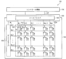
- FIG. 11 is a diagram showing a schematic configuration of a conventional liquid crystal display device 101 that employs a display method in which comb-like electrodes are used in a vertically aligned liquid crystal cell and a fringe electric field is applied.
- the liquid crystal display device 101 includes a liquid crystal panel 102, a flexible printed circuit board 103, a control board 104, and a flexible connection wiring 107.
- the liquid crystal panel 102 has pixels for displaying a plurality of types of colors for each color.
- the plurality of pixels display different colors.
- the different colors here are, for example, the three primary colors of colored light.
- the liquid crystal panel 102 includes a display region 102a, a plurality of gate bus lines (scanning signal lines) GL, a plurality of source bus lines (data signal lines) SL, and a gate driver 105 using amorphous silicon on a glass substrate. It is a built-in active matrix liquid crystal panel. In addition, the liquid crystal panel 102 may be formed using polycrystalline silicon, CG (ContinuoustinGrain) silicon, microcrystalline silicon, or the like.
- the display area 102a is an area in which a plurality of pixels PIX ... are arranged in a matrix.
- the pixel PIX includes a TFT (Thin Film Transistor) 130 which is a selection element of the pixel PIX, a liquid crystal capacitor CL, and an auxiliary capacitor Cs.
- TFT 150 Thin Film Transistor
- the gate of the TFT 150 is connected to the gate bus line GL, the source of the TFT 150 is connected to the source bus line SL, and a voltage corresponding to a data signal described later is input.
- the liquid crystal capacitor CL and the auxiliary capacitor Cs are connected to the drain of the TFT 150.
- the plurality of gate bus lines GL are composed of gate bus lines GL1, GL2, GL3,... GLn, and are connected to the output of the gate driver 105, respectively.
- the plurality of source bus lines SL are made up of source bus lines SL1, SL2, SL3,... SLm, and are connected to the output of the source driver 106, respectively.
- an auxiliary capacitance line is formed that applies an auxiliary capacitance voltage to the auxiliary capacitance Cs that holds the charge of the liquid crystal corresponding to the pixels PIX.
- the gate driver 105 is provided in a region adjacent to one side of the display region 102a on the liquid crystal panel 102 in the direction in which the gate bus lines GL extend, and sequentially supplies gate pulses to the gate bus lines GL. To do.
- the gate driver 105 is monolithically formed with the display region 102a in the liquid crystal panel 102 using amorphous silicon, polycrystalline silicon, CG silicon, microcrystalline silicon, or the like. Gate drivers called gate monolithic, gate driverless, panel built-in gate drivers, gate-in panels, etc. can all be included in the gate driver 105.
- the flexible printed circuit board 103 includes a source driver 106.
- the source driver 106 supplies a data signal to each of the source bus lines SL.
- the control board 104 is connected to the flexible printed circuit board 103 via the flexible connection wiring 107 and supplies necessary signals and power to the gate driver 105 and the source driver 106.
- the signal and power supplied from the control board 104 to the gate driver 105 are supplied to the gate driver 105 through the flexible connection wiring 107 and the flexible printed circuit board 103 and then through the wiring RL routed on the liquid crystal panel 102. Is done.
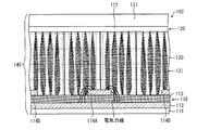
- FIG. 12 is a cross-sectional view schematically showing a schematic configuration of a main part of the liquid crystal panel 102.
- FIG. 13 is a diagram showing a director distribution of liquid crystal molecules in the liquid crystal cell shown in FIG.
- the liquid crystal panel 102 includes a pair of substrates 110 and 120 provided to face each other as an electrode substrate and a counter substrate.
- a liquid crystal layer 130 is sandwiched between the pair of substrates 110 and 120 as a display medium layer.
- At least one of the pair of substrates 110 and 120 that is, at least the viewer-side substrate includes a transparent substrate such as a glass substrate as an insulating substrate.
- alignment films 115 and 122 called so-called vertical alignment films are provided on surfaces of the pair of substrates 110 and 120 facing the other substrate, respectively.
- the vertical alignment film is an alignment film that aligns the liquid crystal molecules of the liquid crystal layer perpendicularly to the substrate surface when no electric field is applied.
- the “vertical” includes “substantially vertical”.
- the substrate 110 for example, an array substrate such as a TFT array substrate can be used.
- the substrate 120 for example, a color filter substrate or the like can be used.
- the substrate 110 may include a TFT or the like (not shown).
- the substrate 120 may include a color filter (CF) (not shown) in addition to the alignment film 122.
- CF color filter
- the substrates 110 and 120 may include an undercoat film or an overcoat film (not shown).
- the display surface side will be described as the upper substrate, and the other substrate will be described as the lower substrate.
- the substrate 110 is described as a lower substrate.
- the substrate 110 has a configuration in which an upper layer electrode 114 and a lower layer electrode 112 are superposed with an insulating layer 113 interposed therebetween.
- the “upper layer electrode” is an electrode on the liquid crystal layer 130 side that is adjacent to the liquid crystal layer 130 via the alignment film 115, and is connected to the source bus line SL via the TFT 150.
- the “lower layer electrode” refers to an electrode on the glass substrate 111 side that is a base substrate.
- the substrate 110 has a configuration in which a lower layer electrode 112, an insulating layer 113, an upper layer electrode 114, and an alignment film 115 are provided in this order on a glass substrate 111.
- the lower layer electrode 112 is a solid electrode, and is disposed on the glass substrate 111 so as to cover a display region of the substrate 110 (that is, a region surrounded by the sealant 134). It is formed over almost the entire surface, and a common voltage is applied.
- the lower layer electrode 112 functions as a common electrode.
- the insulating layer 113 is formed on the lower electrode 112 so as to cover the lower electrode 112.
- the upper layer electrode 114 is composed of comb-like electrodes 114A and 114B and supplied with data signals.
- the comb-like electrodes 114A and 114B may each be linear, or may be formed in a V shape or a zigzag shape.
- the alignment film 115 is provided on the insulating layer 113 so as to cover the comb-shaped electrodes 114A and 114B.
- polarizing plates 135 and 136 are provided on the surfaces of the pair of substrates 110 and 120 opposite to the surfaces facing the liquid crystal layer 130, respectively.
- a retardation plate is provided between the substrate 110 and the polarizing plate 135 and between the substrate 120 and the polarizing plate 136, respectively, as necessary.
- the retardation plate may be provided only on one surface of the liquid crystal panel 102. Further, in the case of a liquid crystal display device using only front transmitted light, the retardation plate is not necessarily essential.
- liquid crystal cell 145 in the liquid crystal panel 102 for example, as shown in FIG. 12, a substrate 110 and a substrate 120 are bonded together by a sealant 134 via a spacer 133, and a liquid crystal material It is formed by enclosing a medium containing
- the liquid crystal material is a p (positive) type liquid crystal material.
- the liquid crystal panel 102 and the liquid crystal display device 101 form a distribution of electric field strength in the liquid crystal cell 145 by applying an electric field, thereby realizing bend alignment of the liquid crystal material.
- the liquid crystal panel 102 is formed by bonding the retardation plate and the polarizing plates 135 and 136 to the liquid crystal cell 145 as described above.
- the transmission axes of the polarizing plates 135 and 136 are orthogonal to each other, and the direction in which the comb electrodes 114A and 114B are extended and the transmission axis of the polarizing plates 135 and 136 are 45 degrees. Arranged at an angle.
- the liquid crystal panel 102 has a configuration similar to the electrode configuration of the liquid crystal panel using a so-called FFS (Fringe Field Switching) mode display method in which the common electrode and the pixel electrode are arranged to overlap with each other through the insulating layer. have.
- FFS Frle Field Switching
- the liquid crystal panel 102 is merely similar in electrode configuration to that of an FFS mode liquid crystal panel, and is different from a so-called FFS mode liquid crystal panel. Therefore, hereinafter, the liquid crystal panel 102 having the configuration of FIG. 12 is referred to as an FFS structure liquid crystal panel, and is distinguished from an FFS mode liquid crystal panel.
- liquid crystal panel using an FFS mode display method when a voltage is not applied, the major axis direction of liquid crystal molecules sandwiched between a pair of substrates shows a homogeneous alignment parallel to the substrate surface.
- the liquid crystal panel 102 exhibits homeotropic alignment in which the major axis direction of the liquid crystal molecules 131 sandwiched between the pair of substrates 110 and 120 is perpendicular to the substrate surface when no voltage is applied, as shown in FIG. ing. For this reason, the liquid crystal panel 102 is completely different from the FFS mode in the behavior of liquid crystal molecules.
- the liquid crystal panel 102 having the FFS structure is driven by two driving methods.
- comb-tooth driving driving performed between the comb-shaped electrode 114A and the comb-shaped electrode 114B that are adjacent to each other via the alignment film 115.
- the driving performed between the comb-shaped electrodes 114A and 114B and the lower layer electrode 112 provided below the comb-shaped electrodes 114A and 114B with the insulating layer 113 interposed therebetween is referred to as “FFS driving”.
- the comb-tooth electrode 114A functions as a pixel electrode
- the comb-tooth electrode 114B functions as a common electrode.
- the lower layer electrode 112 is set to 0V.
- the comb-like electrodes 114A and 114B function as pixel electrodes, and the lower layer electrode 112 functions as a common electrode.
- the liquid crystal panel 102 uses a display method that is completely different from the FFS mode as described above.
- the liquid crystal panel 102 has the FFS structure as described above, not only the interdigital electrodes 114A and 114B but also the liquid crystal molecules 131 on the interdigital electrodes 114A and 114B are driven. For this reason, it has an advantage that the aperture ratio can be increased as compared with the conventional liquid crystal panel that drives only the liquid crystal molecules between the comb-like electrodes 114A and 114B.
- the liquid crystal panel 102 is driven to apply a lateral electric field in the vertical alignment mode.
- the alignment of the liquid crystal molecules 131 becomes a bend shape (bow shape), and two domains whose director directions of the liquid crystal molecules 131 are different from each other by 180 degrees are formed.
- the liquid crystal molecules 131 are arranged according to the electric field strength distribution in the liquid crystal cell 145 and the binding force from the interface. Thereby, a wide viewing angle characteristic can be obtained.
- the liquid crystal molecules 131 continuously change from homeotropic alignment to bend alignment by applying a voltage.
- the liquid crystal layer 130 In normal driving, the liquid crystal layer 130 always exhibits bend alignment as shown in FIG. 13, and a high-speed response is possible with an inter-tone response.
- the inter-tone response is a response that changes the state of liquid crystal molecules from a certain tone value to a target tone value.
- the liquid crystal panel 102 is driven to apply a lateral electric field while maintaining high contrast in the vertical alignment mode as described above. By doing so, the alignment of the liquid crystal molecules 131 is defined. For this reason, alignment control by protrusions like the MVA mode is unnecessary, and the viewing angle characteristic is excellent with a simple pixel configuration.
- the liquid crystal panel 102 has an advantage that high-speed response based on bend alignment and high contrast resulting from the vertical alignment mode can be obtained, and the structure is simple, easy to manufacture, and inexpensive to manufacture. Has the advantage of being able to
- the liquid crystal device according to Patent Document 1 includes a partition wall 11 corresponding to the sealant 134 of the liquid crystal panel 102. This prevents the alignment of the liquid crystal molecules from being distorted when an external force is applied to the random adsorption type cell in the horizontal alignment mode.
- JP 7-43694 A (published on February 14, 1995)
- drive frequency the frequency of the voltage applied between the comb-like electrodes 114A and 114B and the lower layer electrode 112 (hereinafter referred to as “drive frequency”) is 60 Hz, the liquid crystal molecules The strain in the orientation of 131 becomes remarkable. The greater the distortion, the wider the pitch P between two liquid crystal molecules 131 that are continuous in the horizontal direction (see FIG. 14). The wider the pitch P, the more difficult it is for light to pass between the two liquid crystal molecules 131, so the transmittance of the liquid crystal panel 102 decreases.
- the present invention has been made in view of the above-described conventional problems, and an object of the present invention is to provide a liquid crystal display device that has higher transmittance than conventional liquid crystal display devices and can perform double speed driving and 3D driving, and liquid crystal It is to provide a method for driving a display device.
- the liquid crystal display device of the present invention is a liquid crystal display device including an active matrix type liquid crystal panel, and the liquid crystal panel has a matrix substrate, a counter substrate, and a positive dielectric anisotropy. And a liquid crystal layer sandwiched between the matrix substrate and the counter substrate, and an electric field provided on the liquid crystal layer side surface of each of the matrix substrate and the counter substrate are applied. And an alignment film that aligns the liquid crystal molecules of the liquid crystal layer perpendicularly to the substrate surface during the non-period, and the matrix substrate has a first electrode, an insulating layer, a second electrode, and the alignment on the first substrate.
- the film has a structure provided in this order, and the first electrode is formed so as to cover the entire surface of the second electrode as viewed from the first substrate side, and a common voltage is applied.
- the insulating layer is formed on the first electrode so as to cover the first electrode, and the second electrode is a slit electrode or an interdigital electrode that has a slit.
- a driving frequency of a voltage supplied with a data signal and applied between the first electrode and the second electrode is 100 Hz to 450 Hz.
- a conventional liquid crystal display device has a driving frequency of 60 Hz. For this reason, the distortion in the alignment of the liquid crystal molecules becomes remarkable, and the pitch between two liquid crystal molecules continuous in the horizontal direction is widened. The wider the pitch, the more difficult it is for light to pass between the two liquid crystal molecules, thus reducing the transmittance of the liquid crystal panel.
- the inventors of the present invention have found a frequency band in which the driving frequency is 100 Hz to 450 Hz, that is, an optimal frequency band.
- the driving frequency is higher than 60 Hz, and thus the transmittance is higher than that of the conventional liquid crystal display device. Then, it is possible to perform double speed driving in which the driving frequency is set to twice the normal frequency and 3D driving that is a driving to display a three-dimensional image.
- liquid crystal display device that has higher transmittance than conventional liquid crystal display devices and can perform double speed driving or 3D driving.
- a driving method of a liquid crystal display device of the present invention is a driving method of a liquid crystal display device including an active matrix liquid crystal panel, and the liquid crystal panel includes a matrix substrate, a counter substrate, A liquid crystal having a positive dielectric anisotropy is used, and is provided on the liquid crystal layer sandwiched between the matrix substrate and the counter substrate, and on the liquid crystal layer side surfaces of the matrix substrate and the counter substrate. And an alignment film that orients the liquid crystal molecules of the liquid crystal layer perpendicularly to the substrate surface during a period in which an electric field is not applied.
- the matrix substrate includes a first electrode, an insulating layer, a first layer on the first substrate.
- the two electrodes and the alignment film are provided in this order, and the first electrode is formed so as to cover the entire surface of the second electrode when viewed from the first substrate side.
- the insulating layer is formed on the first electrode so as to cover the first electrode
- the second electrode is a slit electrode which is an electrode having a slit, or It is a comb-like electrode, and includes a step of supplying a data signal and setting a driving frequency of a voltage applied between the first electrode and the second electrode to 100 Hz to 450 Hz. .
- a conventional liquid crystal display device has a driving frequency of 60 Hz. For this reason, the distortion in the alignment of the liquid crystal molecules becomes remarkable, and the pitch between two liquid crystal molecules continuous in the horizontal direction is widened. The wider the pitch, the more difficult it is for light to pass between the two liquid crystal molecules, thus reducing the transmittance of the liquid crystal panel.
- the liquid crystal generally has a frequency characteristic that is a characteristic that the luminance decreases as the drive frequency increases. On the other hand, it has also been confirmed that by appropriately setting the driving frequency, the alignment of liquid crystal molecules is stabilized and the luminance is improved.
- the liquid crystal display device driving method includes a step of setting the driving frequency to 100 Hz to 450 Hz. Since the drive frequency is higher than 60 Hz, the transmittance is higher than that of the conventional liquid crystal display device. Then, it is possible to perform double speed driving in which the driving frequency is set to twice the normal frequency and 3D driving that is a driving to display a three-dimensional image.
- the liquid crystal panel uses a matrix substrate, a counter substrate, and a liquid crystal having positive dielectric anisotropy, and is sandwiched between the matrix substrate and the counter substrate.
- the liquid crystal molecules of the liquid crystal layer and the liquid crystal layer of the matrix substrate and the counter substrate, which are provided on the surfaces on the liquid crystal layer side, are aligned perpendicularly to the substrate surface during a period when no electric field is applied.
- the matrix substrate has a configuration in which the first electrode, the insulating layer, the second electrode, and the alignment film are provided in this order on the first substrate.
- the first electrode Is formed so as to cover the entire surface of the second electrode when viewed from the first substrate side, and a common voltage is applied, and the insulating layer covers the first electrode so as to cover the first electrode.
- the electrode is a slit electrode or an electrode having a slit, and a data signal is supplied, and a driving frequency of a voltage applied between the first electrode and the second electrode is 100 Hz to 450 Hz.
- the liquid crystal panel uses a matrix substrate, a counter substrate, and liquid crystal having positive dielectric anisotropy, and the matrix substrate and the counter substrate are used.
- the liquid crystal layer sandwiched between the liquid crystal layer and the liquid crystal layer of the matrix substrate and the counter substrate on the liquid crystal layer side surface during a period in which no electric field is applied.
- the matrix substrate has a configuration in which the first electrode, the insulating layer, the second electrode, and the alignment film are provided in this order on the first substrate.
- the first electrode is formed so as to cover the entire surface of the second electrode when viewed from the first substrate side, and a common voltage is applied, and the insulating layer covers the first electrode. Formed on the first electrode.
- the second electrode is a slit-containing electrode that is an electrode having a slit or a comb-like electrode, and is supplied with a data signal and applied between the first electrode and the second electrode.
- the method includes a step of setting the drive frequency of the voltage to 100 Hz to 450 Hz.
- FIGS. 1 to 9 An embodiment of the present invention will be described with reference to FIGS. 1 to 9 as follows.
- FIG. 2 is a diagram showing a schematic configuration of the liquid crystal display device 1 according to the embodiment of the present invention.
- the liquid crystal display device 1 is a liquid crystal display device including an active matrix liquid crystal panel 2, and includes a liquid crystal panel 2, a flexible printed board 3, a control board 4, and flexible connection wiring 7. Yes.
- the liquid crystal panel 2 has pixels for displaying a plurality of types of colors for each color.
- the plurality of pixels display different colors.
- the different colors here are, for example, the three primary colors of colored light.
- the liquid crystal panel 2 includes a display region 2a, a plurality of gate bus lines (scanning signal lines) GL, a plurality of source bus lines (data signal lines) SL, and a gate driver 5 using amorphous silicon on a glass substrate. It is a built-in active matrix liquid crystal panel. In addition, the liquid crystal panel 2 may be formed using polycrystalline silicon, CG (ContinuoustinGrain) silicon, microcrystalline silicon, or the like.
- the display area 2a is an area where a plurality of pixels PIX ... are arranged in a matrix.
- the pixel PIX includes a TFT (Thin Film Transistor) 30 that is a selection element of the pixel PIX, a liquid crystal capacitor CL, and an auxiliary capacitor Cs.
- TFT Thin Film Transistor
- the gate of the TFT 50 is connected to the gate bus line GL, the source of the TFT 50 is connected to the source bus line SL, and a voltage corresponding to a data signal described later is input.
- the liquid crystal capacitor CL and the auxiliary capacitor Cs are connected to the drain of the TFT 50.
- the plurality of gate bus lines GL are composed of gate bus lines GL1, GL2, GL3,... GLn, and are connected to the output of the gate driver 5, respectively.
- the plurality of source bus lines SL are made up of source bus lines SL1, SL2, SL3,... SLm, and are connected to the output of the source driver 6, respectively.
- an auxiliary capacitance line is formed that applies an auxiliary capacitance voltage to the auxiliary capacitance Cs that holds the charge of the liquid crystal corresponding to the pixels PIX.
- the gate driver 5 is provided on the liquid crystal panel 2 in a region adjacent to the display region 2a on one side in the direction in which the gate bus lines GL extend, and sequentially supplies gate pulses to the gate bus lines GL. To do.
- the gate driver 5 is monolithically formed with the display region 2a in the liquid crystal panel 2 using amorphous silicon, polycrystalline silicon, CG silicon, microcrystalline silicon, or the like. Gate drivers called gate monolithic, gate driverless, panel built-in gate driver, gate-in panel, and the like can all be included in the gate driver 5.
- the flexible printed circuit board 3 includes a source driver 6.
- the source driver 6 supplies a data signal to each of the source bus lines SL.
- the control board 4 is connected to the flexible printed board 3 via the flexible connection wiring 7 and supplies necessary signals and power to the gate driver 5 and the source driver 6.
- the signal and power supplied to the gate driver 5 output from the control board 4 are supplied to the gate driver 5 through the flexible connection wiring 7 and the flexible printed circuit board 3 and then through the wiring RL routed on the liquid crystal panel 2. Is done.
- FIG. 1 is a cross-sectional view schematically showing a schematic configuration of a main part of a liquid crystal panel 2 according to an embodiment of the present invention.
- FIG. 3 is a diagram showing a director distribution of liquid crystal molecules in the liquid crystal cell shown in FIG.
- the liquid crystal panel 2 includes a pair of substrates 10 and 20 provided to face each other as an electrode substrate and a counter substrate.
- the substrate 10 is a matrix substrate
- the substrate 20 is a counter substrate.
- a liquid crystal layer 30 is sandwiched between the pair of substrates 10 and 20 as a display medium layer.
- At least one of the pair of substrates 10 and 20 uses a transparent substrate such as a glass substrate as an insulating substrate that is a substrate for insulating the inside of the liquid crystal panel 2 from the outside of the liquid crystal panel 2. Yes.
- alignment films 15 and 22 called so-called vertical alignment films are respectively provided on the surfaces of the substrate 10 and the substrate 20 on the liquid crystal layer 30 side.
- the vertical alignment film is an alignment film that aligns the liquid crystal molecules of the liquid crystal layer perpendicularly to the substrate surface during a period when no electric field is applied.
- the “vertical” includes “substantially vertical”.
- an array substrate such as a TFT array substrate can be used.
- a color filter substrate or the like can be used as the substrate 10.
- the substrate 10 may include a TFT or the like (not shown).
- the substrate 20 may include a color filter (CF) (not shown) in addition to the alignment film 22.
- CF color filter
- the present embodiment is not limited to this.
- the substrates 10 and 20 may include an undercoat film or an overcoat film (not shown).
- FIG. 1 illustrates the substrate 10 as a lower substrate, the present embodiment is not limited to this.
- the substrate 10 has a configuration in which an upper layer electrode 14 and a lower layer electrode 12 are superposed with an insulating layer 13 interposed therebetween.
- the “upper layer electrode” is an electrode on the liquid crystal layer 30 side that is adjacent to the liquid crystal layer 30 through the alignment film 15, and is connected to the source bus line SL through the TFT 50.
- “Lower layer electrode” refers to an electrode on the glass substrate 11 (first substrate, transparent substrate) side which is a base substrate.
- the substrate 10 has a configuration in which a lower layer electrode 12 (first electrode), an insulating layer 13, an upper layer electrode 14 (second electrode), and an alignment film 15 are provided in this order on a glass substrate 11. is doing.
- the lower layer electrode 12 is a solid electrode, and covers the display region (that is, the region surrounded by the sealant 34) on the glass substrate 11 on the glass substrate 11 (as viewed from the glass substrate 11 side). And a common voltage is applied to the glass substrate 11 over almost the entire surface of the glass substrate 11 facing the substrate 20.
- the lower layer electrode 12 functions as a common electrode.
- the insulating layer 13 is formed on the lower electrode 12 so as to cover the lower electrode 12.
- the upper layer electrode 14 is composed of comb-like electrodes 14A and 14B and is supplied with a data signal.
- the comb-like electrodes 14A and 14B may each be linear, or may be formed in a V shape or a zigzag shape.
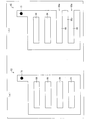
- the comb-like electrodes 14A and 14B are provided so as to be driven independently of each other. For example, they are provided as shown in FIG. That is, the comb-like electrode 14A, which is a branch electrode extending in a direction orthogonal to the linear stem electrode 14C, and the comb-like electrode 14B, which is a branch electrode extending in a direction orthogonal to the linear stem electrode 14D.
- the comb-like electrode 14A which is a branch electrode extending in a direction orthogonal to the linear stem electrode 14C
- the comb-like electrode 14B which is a branch electrode extending in a direction orthogonal to the linear stem electrode 14D.
- a contact hole 71 is provided at one end of the trunk electrode 14C, and a contact hole 72 is provided at one end of the trunk electrode 14D as shown in FIG.
- the contact holes 71 and 72 connect the trunk electrodes 14C and 14D to the drain of the TFT 50.
- the alignment film 15 is provided on the insulating layer 13 so as to cover the comb-shaped electrodes 14A and 14B.
- an arrow A15 indicates the direction of the groove of the alignment film 15, and the comb-like electrodes 14A and 14B and the groove of the alignment film 15 are parallel to each other.
- the present invention is not limited to this, and the comb-like electrodes 14A and 14B and the grooves of the alignment film 15 may be orthogonal to each other.
- polarizing plates 35 and 36 are provided on surfaces of the pair of substrates 10 and 20 opposite to the surfaces facing the liquid crystal layer 30, respectively.
- arrows A35 and A36 indicate the directions of the absorption axes of the polarizing plates 35 and 36, respectively, and the angle formed by the groove of the alignment film 15 and the absorption axis of the polarizing plate 35 is 45 degrees.
- the angle formed by the groove of the alignment film 15 and the absorption axis of the polarizing plate 36 is 45 degrees.
- the absorption axis of the polarizing plate 35 and the absorption axis of the polarizing plate 36 have a crossed Nicols relationship.
- a retardation plate is provided between the substrate 10 and the polarizing plate 35 and between the substrate 20 and the polarizing plate 36 as necessary.
- the retardation plate may be provided only on one surface of the liquid crystal panel 2. Further, in the case of a liquid crystal display device using only front transmitted light, the retardation plate is not necessarily essential.
- the liquid crystal cell 45 in the liquid crystal panel 2 includes a substrate 10 and a substrate 20 that are bonded together with a sealant 34 via a spacer 33, and a liquid crystal material is provided in the gap between the substrates 10 and 20. It is formed by enclosing a medium containing
- the liquid crystal material is a p (positive) type liquid crystal material (a liquid crystal material having positive dielectric anisotropy).
- a p-type nematic liquid crystal material can be used as the p-type liquid crystal material, but the present embodiment is not limited to this.
- the liquid crystal panel 2 and the liquid crystal display device 1 are configured to form a distribution of electric field strength in the liquid crystal cell 45 by applying an electric field, thereby realizing bend alignment of the liquid crystal material.
- the liquid crystal panel 2 is formed by bonding the retardation plate and the polarizing plates 35 and 36 to the liquid crystal cell 45 as described above.
- the transmission axes of the polarizing plates 35 and 36 are orthogonal to each other, and the direction in which the comb electrodes 14A and 14B are extended and the transmission axis of the polarizing plates 35 and 36 are 45 degrees. Arranged at an angle.
- the liquid crystal panel 2 described above is referred to as an FFS structure liquid crystal panel, as described in the background art.
- the liquid crystal panel 2 having the FFS structure is driven by two driving methods.
- comb-tooth driving driving that drives between the comb-like electrode 14A and the comb-like electrode 14B that are adjacent to each other via the alignment film 15
- driving that performs driving between the comb-shaped electrodes 14A and 14B and the lower layer electrode 12 provided below the comb-shaped electrodes 14A and 14B with the insulating layer 13 interposed therebetween is referred to as “FFS driving”.
- the comb electrode 14A functions as a pixel electrode
- the comb electrode 14B functions as a common electrode. Note that when the comb driving is performed, the lower layer electrode 12 is set to 0V.
- the comb-like electrodes 14A and 14B each function as a pixel electrode, and the lower layer electrode 12 functions as a common electrode.
- the liquid crystal panel 2 uses a display method that is completely different from the FFS mode as described above.
- the liquid crystal panel 2 has the FFS structure as described above, not only the interdigital electrodes 14A and 14B but also the liquid crystal molecules 31 on the interdigital electrodes 14A and 14B are driven. For this reason, there is an advantage that the aperture ratio can be increased as compared with the conventional liquid crystal panel that drives only the liquid crystal molecules between the comb-like electrodes 14A and 14B.
- the liquid crystal panel 2 is driven to apply a lateral electric field in the vertical alignment mode.
- the orientation of the liquid crystal molecules 31 becomes a bend shape (bow shape), and two domains in which the director directions of the liquid crystal molecules 31 are different from each other by 180 degrees are formed.
- the liquid crystal molecules 31 are arranged according to the electric field strength distribution in the liquid crystal cell 45 and the binding force from the interface. Thereby, a wide viewing angle characteristic can be obtained.
- the liquid crystal molecules 31 continuously change from homeotropic alignment to bend alignment by applying a voltage.
- the liquid crystal layer 30 In normal driving, the liquid crystal layer 30 always exhibits bend alignment as shown in FIG. 1, and a high-speed response is possible with an inter-tone response.
- the inter-tone response is a response that changes the state of liquid crystal molecules from a certain tone value to a target tone value.
- the liquid crystal panel 2 is driven to apply a lateral electric field while maintaining high contrast in the vertical alignment mode as described above. By doing so, the alignment of the liquid crystal molecules 31 is defined. For this reason, alignment control by protrusions like the MVA mode is unnecessary, and the viewing angle characteristic is excellent with a simple pixel configuration.
- the liquid crystal panel 2 has the advantages that high-speed response based on bend alignment and high contrast resulting from the vertical alignment mode can be obtained, and the structure is simple, easy to manufacture, and inexpensive to manufacture. Has the advantage of being able to
- the liquid crystal panel 2 according to the present embodiment is manufactured by, for example, the following process.
- the lower electrode 12 covering the entire surface of the glass substrate 11 was formed by forming ITO with a thickness of 1400 mm on the glass substrate 11 by sputtering.
- an insulating layer 13 covering the entire surface of the lower layer electrode 12 was formed by sputtering.
- the thickness of the insulating layer 13 was 0.3 ⁇ m.
- comb-like electrodes 14A and 14B made of ITO were provided on the insulating layer 13.
- the width W of the comb-like electrodes 14A and 14B was 2.5 ⁇ m.
- the thickness of the comb-like electrodes 14A and 14B was 1400 mm.
- an interval D of 8 ⁇ m was provided between the comb-shaped electrode 14A and the comb-shaped electrode 14B.
- JALS-204 (5 wt.%, ⁇ -butyrolactone solution), which is an alignment film paint manufactured by JSR, was applied on the glass substrate 11 having undergone the above steps by spin coating, and then at 200 ° C. for 2 hours. Baked.
- the substrate 20 which is a glass substrate facing the glass substrate 11, was similarly applied with an alignment film paint JALS-204 (5 wt.%, ⁇ -butyrolactone solution) manufactured by JSR by spin coating, and then 200 ° C. For 2 hours.
- JALS-204 5 wt.%, ⁇ -butyrolactone solution
- the thickness of the alignment film 15 provided on the substrate 10 after firing described above was 1000 mm.
- the thickness of the alignment film provided on the substrate 20 was 1000 mm.
- a liquid crystal material having a large refractive index anisotropy ⁇ n or a liquid crystal material having a large dielectric anisotropy ⁇ is preferably used.
- p-type liquid crystal materials include CN (cyano) liquid crystal materials (chiral nematic liquid crystal materials) and F (fluorine) liquid crystal materials.
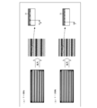
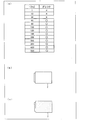
- FIG. 5A is a diagram showing the pitch P when the drive frequency f is 60 Hz
- FIG. 5B is a diagram showing the pitch P when the drive frequency f is 300 Hz.
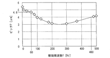
- FIG. 6 is a graph showing the measurement result of the pitch P corresponding to the drive frequency f.
- the drive frequency f is changed from 1 Hz to 500 Hz.
- FIG. 6 confirms that the pitch P is less than 4 ⁇ m when the drive frequency f is about 100 Hz to about 460 Hz (particularly about 100 Hz to 300 Hz).
- the drive frequency of the liquid crystal panel is set to 60 Hz.
- the drive frequency f is set to a high frequency of about 240 Hz.
- the drive frequency f of about 100 Hz to 460 Hz (especially about 100 Hz to 300 Hz) with improved transmittance this time can be suitably used for a liquid crystal display device that performs double speed driving or 3D driving.
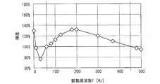
- the driving frequency f was changed, and photography using an optical microscope and a CCD camera was performed using the same luminance (background) as a reference (REF).
- the luminance of one pixel (area) was calculated by performing image processing on the photograph taken.
- the graph of FIG. 7 shows how much the luminance calculated at each driving frequency is 100% when the driving frequency f is 60 Hz.
- the graphs of FIGS. 6 and 7 are graphs created by obtaining a statistically optimal approximate curve for a large number of plots obtained by simulation and experiment, and the illustrated plots are easy to understand. It is simplified for the sake of convenience.
- FIG. Shown in a the result of confirming whether or not roughness in the lighting state of the liquid crystal panel 2 due to the alignment in the region where the alignment pitch is long (the low frequency where the drive frequency f is less than 60 Hz) is performed is shown in FIG. Shown in a).
- FIG. 8A when the driving frequency f is 60 Hz or more, no roughness is generated as shown in FIG. 8B, and when the driving frequency f is less than 60 Hz, FIG. As shown, it was confirmed that roughness occurred. Therefore, by setting the drive frequency f to 60 Hz or more, it is possible to prevent the quality of the displayed image from deteriorating.
- the luminance improvement effect is particularly excellent when the driving frequency f at which the alignment of liquid crystal molecules is stabilized is in the range of 100 Hz to 300 Hz. It was also found that the luminance improvement effect was excellent even when the drive frequency f was in the range of 60 Hz to 100 Hz and the drive frequency f was in the range of 300 Hz to 450 Hz.
- the liquid crystal generally has a frequency characteristic that is a characteristic that the luminance decreases as the drive frequency f increases.
- the driving frequency f it has also been confirmed that by appropriately setting the driving frequency f, the alignment of the liquid crystal molecules 31 is stabilized and the luminance is improved.
- the inventors of the present invention have found a frequency band in which the drive frequency f is 100 Hz to 450 Hz, that is, an optimal frequency band.
- the driving frequency f is higher than 60 Hz, and thus the transmittance is higher than that of the conventional liquid crystal display device. Then, it is possible to perform double speed driving in which driving frequency f is set to twice the normal frequency, or 3D driving, which is a driving to display a three-dimensional image.
- liquid crystal display device that has higher transmittance than conventional liquid crystal display devices and can perform double speed driving or 3D driving.
- the driving frequency may be not less than 100 Hz and not more than 300 Hz. Thereby, the alignment of the liquid crystal molecules is further stabilized, so that the luminance is further improved.
- the driving frequency may be 120 Hz. As a result, it is possible to perform double speed driving in which the driving frequency is set to twice the normal frequency.
- the first electrode may be a solid electrode.
- the first electrode can cover the entire surface of the second electrode as viewed from the first substrate side.
- the first substrate may be a transparent substrate.
- the inside of the liquid crystal panel and the outside of the liquid crystal panel can be insulated.
- the comb-like electrodes 14A and 14B are provided in order to generate a lateral electric field that is an electric field parallel to the substrate surface.
- the comb-like electrodes 14A and 14B are different from each other.
- a transverse electric field may be generated by providing the electrodes.
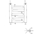
- FIG. 9 is a plan view of the slit electrode 60 according to the embodiment of the present invention. 9 is provided on the insulating layer 13 in the same manner as the comb-like electrodes 14A and 14B in FIG.
- the “slit electrode” is, for example, a rectangular electrode (second electrode) that functions as a pixel electrode. By removing (removing) a part of the electrode, a slit (gap) is formed at the extracted location. It is an electrode provided.
- the two slits 61 are provided by extracting the pixel electrode at two locations.
- the number of locations to be extracted is Not particularly limited.
- the two slits 61 are both surrounded by electrodes.
- the slit electrode according to the present embodiment is not limited to this, and a comb-like electrode may be formed by providing a slit.
- An example of the slit-containing electrode on which such a comb-like electrode is formed will be described in [Modified example of slit-containing electrode] below.
- the slit-containing electrode 60 of FIG. 9 two slits 61 are provided.
- a horizontal electric field is generated in the slit electrode 60 in the direction indicated by the arrow in FIG. 9, a part of the lines of electric force generated from the slit electrode 60 are transferred to the solid lower electrode 12 through the slit 61. Reach the phenomenon.
- the slit electrode 60 is provided with a contact hole 73. Through the contact hole 73, the slit electrode 60 is connected to the drain of the TFT 50.
- the slit electrode 60 is composed of a linear electrode portion 60A corresponding to the comb-like electrodes 14A and 14B and a linear electrode portion 60B corresponding to the trunk electrodes 14C and 14D. And the slit 61 is formed in the inside of a rectangle by forming a rectangle with two electrode parts 60A and two electrode parts 60B which counter.
- the slit-containing electrode 60 in FIG. 9 has two slits 61 formed in this way.
- the direction of the electric field E1 in the electrode part 60A is different from the direction of the electric field E2 in the electrode part 60B by 90 degrees.
- the liquid crystal molecules 31 are continuously aligned as shown in FIG. 9 with the electrode portion 60B as an end.
- the driving frequency f is changed, the periodicity of the alignment of the liquid crystal molecules 31 changes.
- the portion with the shortest periodicity is the region where the orientation is most stabilized, and the rate of decrease in transmittance due to the dark line 62 becoming wavy is the lowest.
- the pitch P becomes as fine as less than 4 ⁇ m, so that the alignment state of the liquid crystal molecules is stabilized and the transmittance is increased. Said to improve. That the pitch P becomes smaller means that the wavy dark line 62 becomes closer to a straight line.
- the pitch P and the luminance in the case of a liquid crystal display device using linearly polarized light, an axis that forms an angle of ⁇ 45 degrees with respect to the direction of the liquid crystal domain (for example, the groove direction of the alignment film 15)
- the absorption axes are 35 and 36. That is, the absorption axes of the polarizing plates 35 and 36 are arranged to be crossed Nicols.
- the phase difference between the polarization components of the two lights in the plane perpendicular to the light traveling direction is 180 degrees (1). / 2 ⁇ ).
- the light absorbed in the absorption axis of the polarizing plate 35 is transmitted through the absorption axis of the polarizing plate 36 that forms an angle of 45 degrees with respect to the direction of the liquid crystal domain.
- the area of the wavy dark line 62 is an area where light loss occurs and does not contribute to luminance.
- FIG. 10 is an explanatory view of a modified example of the slit electrode
- FIGS. 10A and 10B are plan views showing modified examples of the slit electrode.
- the slit-equipped electrode 63 in FIG. 10A four rectangular slits 64 are provided by extracting four positions from a rectangular electrode (second electrode).
- the slit electrode 63 is provided with a contact hole 74. Through the contact hole 74, the slit electrode 63 is connected to the drain of the TFT 50.
- 10 (b) is the same as the slit electrode 63 in FIG. 10 (a) in that four electrodes are extracted from a rectangular electrode (second electrode).
- the difference between the slit electrode 65 and the slit electrode 63 is the slit structure.
- the four slits 64 in FIG. 10A have a structure surrounded by electrodes.
- two of the four slits in FIG. 10A are the above-described slits 64, but the remaining two are comb-teeth forming slits 66.
- the comb-teeth forming slit 66 is rectangular like the slit 64, but an opening 66a is formed by completely extracting the electrode in one direction. Therefore, the electrode 66b sandwiched between the two comb-forming slits 66 becomes a comb-like electrode, like the comb-like electrode 14A of FIG. That is, the electrode 65 having the slit 64 and the electrode 66b which is a comb-like electrode may be combined to form the slit electrode 65.
- a driving method of a liquid crystal display device of the present invention is a driving method of a liquid crystal display device including an active matrix liquid crystal panel, and the liquid crystal panel includes a matrix substrate, a counter substrate, A liquid crystal having a positive dielectric anisotropy is used, and is provided on the liquid crystal layer sandwiched between the matrix substrate and the counter substrate, and on the liquid crystal layer side surfaces of the matrix substrate and the counter substrate.
- an alignment film that orients the liquid crystal molecules of the liquid crystal layer perpendicularly to the substrate surface during a period in which an electric field is not applied
- the matrix substrate has a first electrode, an insulating layer,
- the second electrode and the alignment film are provided in this order, and the first electrode is formed so as to cover the entire surface of the second electrode when viewed from the first substrate side.
- the insulating layer is formed on the first electrode so as to cover the first electrode, and the second electrode is a slit electrode or a comb that is an electrode having a slit. It is a toothed electrode, and includes a step of supplying a data signal and setting a driving frequency of a voltage applied between the first electrode and the second electrode to 100 Hz to 450 Hz.
- a conventional liquid crystal display device has a driving frequency of 60 Hz. For this reason, the distortion in the alignment of the liquid crystal molecules becomes remarkable, and the pitch between two liquid crystal molecules continuous in the horizontal direction is widened. The wider the pitch, the more difficult it is for light to pass between the two liquid crystal molecules, thus reducing the transmittance of the liquid crystal panel.
- the liquid crystal generally has a frequency characteristic that is a characteristic that the luminance decreases as the drive frequency increases. On the other hand, it has also been confirmed that by appropriately setting the driving frequency, the alignment of liquid crystal molecules is stabilized and the luminance is improved.
- the liquid crystal display device driving method includes a step of setting the driving frequency to 100 Hz to 450 Hz. Since the drive frequency is higher than 60 Hz, the transmittance is higher than that of the conventional liquid crystal display device. Then, it is possible to perform double speed driving in which the driving frequency is set to twice the normal frequency and 3D driving that is a driving to display a three-dimensional image.
- the driving frequency may be set to 100 Hz or more and 300 Hz or less in the step. Thereby, the alignment of the liquid crystal molecules is further stabilized, so that the luminance is further improved.
- the driving frequency may be 120 Hz in the step. As a result, it is possible to perform double speed driving in which the driving frequency is set to twice the normal frequency.
- the first electrode may be a solid electrode.
- the first electrode can cover the entire surface of the second electrode as viewed from the first substrate side.
- the first substrate may be a transparent substrate.
- the inside of the liquid crystal panel and the outside of the liquid crystal panel can be insulated.
- the driving frequency may be not less than 100 Hz and not more than 300 Hz. Thereby, the alignment of the liquid crystal molecules is further stabilized, so that the luminance is further improved.
- the driving frequency may be 120 Hz. As a result, it is possible to perform double speed driving in which the driving frequency is set to twice the normal frequency.
- the electrode with slit may be an electrode in which the slit that is a gap is provided at a portion removed by removing a part of the second electrode. Thereby, a transverse electric field which is an electric field parallel to the substrate surface can be generated.
- the first electrode may be a solid electrode.
- the first electrode can cover the entire surface of the second electrode as viewed from the first substrate side.
- the first substrate may be a transparent substrate.
- the inside of the liquid crystal panel and the outside of the liquid crystal panel can be insulated.
- the driving frequency may be set to 100 Hz or more and 300 Hz or less in the step. Thereby, the alignment of the liquid crystal molecules is further stabilized, so that the luminance is further improved.
- the driving frequency may be 120 Hz in the step. As a result, it is possible to perform double speed driving in which the driving frequency is set to twice the normal frequency.
- the slit electrode is an electrode in which the slit that is a gap is provided in a removed portion by removing a part of the second electrode. Also good. Thereby, a transverse electric field which is an electric field parallel to the substrate surface can be generated.
- the first electrode may be a solid electrode.
- the first electrode can cover the entire surface of the second electrode as viewed from the first substrate side.
- the first substrate may be a transparent substrate.
- the inside of the liquid crystal panel and the outside of the liquid crystal panel can be insulated.
- a transmissivity higher than that of a conventional liquid crystal display device and a liquid crystal display device capable of performing double speed driving or 3D driving and a driving method of the liquid crystal display device can be provided. It can be suitably used for a liquid crystal display device capable of performing the above.
Landscapes
- Engineering & Computer Science (AREA)
- Multimedia (AREA)
- Signal Processing (AREA)
- Liquid Crystal (AREA)
Abstract
従来の液晶表示装置よりも透過率が高く、倍速駆動や3D駆動を行うことが出来る液晶表示装置、及び液晶表示装置の駆動方法を提供する。液晶表示装置(1)の液晶パネル(2)は、基板(10)と、基板(20)と、基板(10)と基板(20)との間に挟持された液晶層(30)と、基板(10)及び基板(20)のそれぞれの液晶層(30)側の面に設けられた配向膜(15・22)とを備えるとともに、基板(10)は、ガラス基板(11)上に、下層電極(12)、絶縁層(13)、上層電極(14)、配向膜(15)が、この順に設けられ、下層電極(12)は、ガラス基板(11)側から見て、上層電極(14)の全面を覆うように形成され、コモン電圧が印加され、絶縁層(13)は、下層電極(12)を覆うように形成され、上層電極(14)は、櫛歯状電極(14A・14B)であり、データ信号が供給され、下層電極(12)と上層電極(14)との間に印加される電圧の駆動周波数fは、100Hz以上450Hz以下である。
Description
本発明は、液晶表示装置及び液晶表示装置の駆動方法に関するものである。
液晶表示装置は、各種表示装置のなかでも薄型で軽量かつ消費電力が小さいといった利点を有し、近年、CRTに代わって、TV、モニタ、携帯電話等のモバイル機器等の様々な分野で広く用いられている。
液晶表示装置の表示方式は、液晶セル内で液晶をどのように配列させるかによって決定される。
液晶表示装置の表示方式の一つとして、従来、MVA(Multi-domain Vertical Alignment)モードの液晶表示装置が知られている。MVAモードは、アクティブマトリクス基板の画素電極にスリットを設けるとともに、対向基板の対向電極に液晶分子配向制御用の突起(リブ)を設け、これによって垂直方向の電界を加え、リブやスリットで配向方向を規制しながら液晶分子の配向方向を複数方向に配設させる方式である。
MVAモードの液晶表示装置は、電界印加時に液晶分子が倒れる方向を複数に分割することによって、広視野角を実現している。また、垂直配向モードであるため、IPS(In-Plain Switching)モード等の水平配向モードに比べて高コントラストを得ることができる。しかしながら、製造工程が複雑であるという欠点を有している。
そこで、MVAモードの製造工程に関する課題を解決すべく、電圧無印加時に液晶分子が基板垂直方向に配向する垂直配向型の液晶セル(垂直配向セル)に櫛歯状電極を使用し、基板面に平行な電界(いわゆる横電界(フリンジ電界))を印加する表示方式が提案されている。垂直配向型の液晶セルに横電界を印加して、液晶分子を水平に配列するモードを、TBA(Transverse Bend Alignment)モードという。
上記表示方式では、垂直配向モードによる高コントラスト性を保ちながら横電界により駆動させることで液晶分子の配向方位を規定する。上記表示方式は、MVAのような突起物による配向制御が不要であるため、画素構成が単純であり、優れた視野角特性を有している。
図11は、垂直配向型の液晶セルに櫛歯状電極を使用し、フリンジ電界を印加する表示方式を採用した従来の液晶表示装置101の概要構成を示す図である。図11に示すように、液晶表示装置101は、液晶パネル102、フレキシブルプリント基板103、コントロール基板104、及びフレキシブル接続配線107を備えている。液晶パネル102は、複数種類の色を表示する画素を色毎に有している。これらの複数の画素は、互いに異なる色を表示する。ここでいう互いに異なる色とは、たとえば色光の三原色のことである。
液晶パネル102は、ガラス基板上にアモルファスシリコンを用いて表示領域102a、複数のゲートバスライン(走査信号線)GL…、複数のソースバスライン(データ信号線)SL…、および、ゲートドライバ105が作りこまれたアクティブマトリクス型の液晶パネルである。この他に、液晶パネル102は、多結晶シリコン、CG(Continuous Grain)シリコン、微結晶シリコンなどを用いて形成されていてもよい。
表示領域102aは、複数の画素PIX…がマトリクス状に配置された領域である。画素PIXは、画素PIXの選択素子であるTFT(Thin Film Transistor:薄膜トランジスタ)130、液晶容量CL、および、補助容量Csを備えている。スイッチング素子としてTFT150を用いることにより、液晶パネル102の薄型化が可能となる。
TFT150のゲートはゲートバスラインGLに接続されており、TFT150のソースはソースバスラインSLに接続されており、後述するデータ信号に応じた電圧が入力される。液晶容量CLおよび補助容量CsはTFT150のドレインに接続されている。
複数のゲートバスラインGL…はゲートバスラインGL1・GL2・GL3・…・GLnからなり、それぞれゲートドライバ105の出力に接続されている。複数のソースバスラインSL…はソースバスラインSL1・SL2・SL3・…・SLmからなり、それぞれソースドライバ106の出力に接続されている。また、図示しないが、画素PIX…に対応する液晶の電荷を保持する補助容量Csに補助容量電圧を与える補助容量配線が形成されている。
ゲートドライバ105は、液晶パネル102上で表示領域102aに対してゲートバスラインGL…の延びる方向の一方側に隣接する領域に設けられており、ゲートバスラインGL…のそれぞれに順次ゲートパルスを供給する。このゲートドライバ105は、液晶パネル102に、アモルファスシリコンや多結晶シリコン、CGシリコン、微結晶シリコンなどを用いて、表示領域102aとモノリシックに作りこまれている。ゲートモノリシック、ゲートドライバレス、パネル内蔵ゲートドライバ、ゲートインパネルなどと称されるゲートドライバは全て、ゲートドライバ105に含まれ得る。
フレキシブルプリント基板103は、ソースドライバ106を備えている。ソースドライバ106は、ソースバスラインSL…のそれぞれにデータ信号を供給する。コントロール基板104は、フレキシブル接続配線107を介してフレキシブルプリント基板103に接続されており、ゲートドライバ105およびソースドライバ106に必要な信号や電源を供給する。コントロール基板104から出力されたゲートドライバ105へ供給する信号および電源は、フレキシブル接続配線107およびフレキシブルプリント基板103を介した後、液晶パネル102上に引き回された配線RLを通して、ゲートドライバ105へ供給される。
図12は、液晶パネル102の要部の概略構成を模式的に示す断面図である。また、図13は、図12に示す液晶セル内の液晶分子のダイレクタ分布を示す図である。
図12に示すように、液晶パネル102は、電極基板および対向基板として、互いに対向して設けられた一対の基板110・120を備えている。これら一対の基板110・120間には、表示用の媒質層として液晶層130が挟持されている。
また、上記一対の基板110・120のうち少なくとも一方の基板、つまり、少なくとも観察者側の基板は、絶縁基板として、ガラス基板等の透明基板を備えている。また、上記一対の基板110・120における他方の基板との対向面には、いわゆる垂直配向膜と称される配向膜115・122がそれぞれ設けられている。
垂直配向膜は、電界無印加時に液晶層の液晶分子を基板面に垂直に配向させる配向膜である。なお、上記「垂直」には、「略垂直」も含まれる。
基板110としては、例えば、TFTアレイ基板等のアレイ基板を用いることができる。一方、基板120としては、例えば、カラーフィルタ基板等を用いることができる。
すなわち、基板110は、図示しないTFT等を備えていてもよい。また、基板120は、配向膜122の他に、図示しないカラーフィルタ(CF)を備えていてもよい。
また、基板110・120が、図示しないアンダーコート膜やオーバーコート膜等を備えていてもよいことは言うまでも無い。
以下、表示面側を上側の基板とし、他方の基板を下側の基板として説明する。また、図12では、基板110を下側の基板として説明する。
基板110は、上層電極114と下層電極112とが、絶縁層113を介して重畳配置された構成を有している。なお、「上層電極」とは、配向膜115を介して液晶層130と隣り合う、液晶層130側の電極であり、TFT150を介してソースバスラインSLに接続されている。「下層電極」とは、ベース基板であるガラス基板111側の電極を示す。
具体的には、基板110は、ガラス基板111上に、下層電極112、絶縁層113、上層電極114、配向膜115が、この順に設けられた構成を有している。
下層電極112はベタ状の電極であり、ガラス基板111上に、基板110における表示領域(すなわち、シール剤134で囲まれた領域)を覆うように、ガラス基板111における基板120との対向面のほぼ全面に渡って形成されており、コモン電圧が印加される。下層電極112は、共通電極として機能する。
絶縁層113は、下層電極112を覆うように、下層電極112上に形成されている。
上層電極114は、櫛歯状電極114A・114Bで構成されており、データ信号が供給される。櫛歯状電極114A・114Bは、それぞれ、直線状であってもよく、V字状あるいはジグザグ状に形成されていてもよい。
配向膜115は、櫛歯状電極114A・114Bを覆うように、絶縁層113上に設けられている。
また、図12に示すように、これら一対の基板110・120における液晶層130との対向面とは反対側の面には、偏光板135・136がそれぞれ設けられている。
また、基板110と偏光板135との間、及び、基板120と偏光板136との間には、必要に応じて位相差板がそれぞれ設けられている。但し、上記位相差板は、液晶パネル102の一方の面にのみ設けられていてもよい。また、正面透過光のみを利用する液晶表示装置の場合には、上記位相差板は必ずしも必須ではない。
液晶パネル102における液晶セル145は、例えば、図12に示すように、基板110と基板120とを、スペーサ133を介してシール剤134によって貼り合わせ、両基板110・120間の空隙に、液晶材料を含む媒質を封入することにより形成される。上記液晶材料は、p(ポジ)型の液晶材料である。
液晶パネル102および液晶表示装置101は、電界の印加により、液晶セル145内に電界強度の分布を形成し、液晶材料のベンド配向を実現するものである。
液晶パネル102は、上記したように、位相差板および偏光板135・136を液晶セル145に貼り合わせることにより形成される。
偏光板135・136は、例えば、偏光板135・136の透過軸が互いに直交し、かつ、櫛歯状電極114A・114Bが延伸される方向と偏光板135・136の透過軸とが45度の角度をなすように配置される。
以上のように、液晶パネル102は、共通電極と画素電極とが絶縁層を介して重畳配置される、いわゆるFFS(Fringe Field Switching)モードの表示方式を用いた液晶パネルの電極構成に類似の構成を有している。
しかしながら、液晶パネル102は、単に電極構成がFFSモードの液晶パネルの電極構成に類似しているにすぎず、いわゆるFFSモードの液晶パネルとは異なるものである。したがって、以下、図12の構成を有する液晶パネル102を、FFS構造の液晶パネルと称し、FFSモードの液晶パネルとは区別する。
FFSモードの表示方式を用いた液晶パネルでは、電圧を印加していない時に、一対の基板間に挟まれた液晶分子の長軸方向が基板面に平行なホモジニアス配向を示している。これに対し、液晶パネル102は、電圧無印加時に、図12に示すように、一対の基板110・120間に挟まれた液晶分子131の長軸方向が基板面に垂直なホメオトロピック配向を示している。このため、液晶パネル102は、FFSモードとは、液晶分子の挙動が全く異なっている。
上記したようにFFS構造を有する液晶パネル102は、2通りの駆動方法により駆動される。
以下、配向膜115を介して隣り合う、櫛歯状電極114Aと櫛歯状電極114Bとの間で行う駆動を「櫛歯駆動」と称する。また、櫛歯状電極114A・114Bと、絶縁層113を挟んで櫛歯状電極114A・114Bの下層に設けられた下層電極112との間で行う駆動を、「FFS駆動」と称する。
液晶パネル102を櫛歯駆動する場合、櫛歯状電極114Aは、画素電極として機能し、櫛歯状電極114Bは、共通電極として機能する。なお、櫛歯駆動を行う場合には、下層電極112は0Vに設定される。
また、液晶パネル102をFFS駆動する場合、櫛歯状電極114A・114Bは、それぞれ画素電極として機能し、下層電極112は、共通電極として機能する。
液晶パネル102は、上記したようにFFSモードとは全く異なる表示方式を用いたものである。
しかしながら、液晶パネル102は、上記したようにFFS構造を有していることで、櫛歯状電極114A・114B間のみならず、櫛歯状電極114A・114B上の液晶分子131も駆動される。このため、櫛歯状電極114A・114B間の液晶分子のみを駆動する従来の液晶パネルと比較して、開口率を大きくすることができるという利点を有している。
また、液晶パネル102は、上記したように、垂直配向モードにおいて横電界を印加する駆動を行う。こうすることで、図13に示すように、液晶分子131の配向がベンド状(弓なり状)となり、液晶分子131のダイレクタ方位が互いに180度異なる2つのドメインが形成される。液晶分子131は、液晶セル145内の電界強度分布、および界面からの束縛力に応じて配列する。これにより、広い視野角特性を得ることができる。
なお、液晶分子131は、電圧印加により、ホメオトロピック配向からベンド配向へと連続的に変化する。通常の駆動においては、液晶層130は、図13に示すように常にベンド配向を呈し、階調間応答で高速応答が可能となる。階調間応答とは、ある階調値から目的の階調値へ液晶分子の状態を遷移させる応答である。
また、液晶パネル102では、上記したように垂直配向モードによる高コントラスト性を保ちながら横電界を印加する駆動を行う。こうすることで、液晶分子131の配向を規定している。このため、MVAモードのような突起物による配向制御が不要であり、単純な画素構成で優れた視野角特性を有している。
したがって、液晶パネル102は、ベンド配向に基づく高速応答性、垂直配向モードに起因する高コントラストを得ることができるという利点を有するとともに、構造がシンプルであり、製造が容易で、安価に製造することができるという利点を有している。
特許文献1に係る液晶装置は、液晶パネル102のシール剤134に相当する隔壁11を備えている。これにより、水平配向モードでランダム吸着型のセルにおいて外力が加えられた場合に、液晶分子の配向がひずむことを防止している。
上述した液晶表示装置101における「FFS駆動」では、図13に示すように、櫛歯状電極114Aから発せられる電気力線が、ベタ状の下層電極112に達することで液晶層が駆動される。
上述した液晶層の駆動を行う際に、櫛歯状電極114A・114Bと下層電極112との間に印加される電圧の周波数(これ以降「駆動周波数」と称する)が60Hzであると、液晶分子131の配向におけるひずみが顕著となる。このひずみが顕著であればあるほど、水平方向において連続する2つの液晶分子131間のピッチPが広い(図14参照)。ピッチPが広くなればなるほど、2つの液晶分子131間で光が透過し難くなるので、液晶パネル102の透過率が低下する。
本発明は、上記従来の問題点に鑑みなされたものであって、その目的は、従来の液晶表示装置よりも透過率が高く、倍速駆動や3D駆動を行うことが出来る液晶表示装置、及び液晶表示装置の駆動方法を提供することにある。
本発明の液晶表示装置は、上記課題を解決するために、アクティブマトリクス型の液晶パネルを備える液晶表示装置であって、上記液晶パネルは、マトリクス基板と、対向基板と、誘電異方性が正である液晶が使用され、上記マトリクス基板と上記対向基板との間に挟持された液晶層と、上記マトリクス基板及び上記対向基板のそれぞれの上記液晶層側の面に設けられた、電界が印加されていない期間に上記液晶層の液晶分子を基板面に垂直に配向させる配向膜とを備えるとともに、上記マトリクス基板は、第1基板上に、第1電極、絶縁層、第2電極、および上記配向膜が、この順に設けられた構成を有しており、上記第1電極は、上記第1基板側から見て、上記第2電極の全面を覆うように形成されているとともに、コモン電圧が印加され、上記絶縁層は、上記第1電極を覆うように、上記第1電極上に形成されており、上記第2電極は、スリットを有する電極であるスリット入り電極、または、櫛歯状電極であるとともに、データ信号が供給され、上記第1電極と上記第2電極との間に印加される電圧の駆動周波数は、100Hz以上450Hz以下であることを特徴とする。
従来の液晶表示装置では一般的に、駆動周波数が60Hzであった。このため、液晶分子の配向におけるひずみが顕著となり、水平方向において連続する2つの液晶分子間のピッチが広くなっていた。ピッチが広くなればなるほど、2つの液晶分子間で光が透過し難くなるので、液晶パネルの透過率が低下していた。
そこで、本発明の発明者は、駆動周波数が100Hz以上450Hz以下である周波数帯、即ち、最適な周波数帯を見出した。この最適な周波数帯では、駆動周波数が60Hzよりも高いので、従来の液晶表示装置よりも透過率が高い。そして、駆動周波数を通常時の2倍の周波数にして駆動を行う倍速駆動や、3次元画像を表示する駆動である3D駆動を行うことが出来る。
従って、従来の液晶表示装置よりも透過率が高く、倍速駆動や3D駆動を行うことが出来る液晶表示装置を提供することが出来る。
本発明の液晶表示装置の駆動方法は、上記課題を解決するために、アクティブマトリクス型の液晶パネルを備える液晶表示装置の駆動方法であって、上記液晶パネルは、マトリクス基板と、対向基板と、誘電異方性が正である液晶が使用され、上記マトリクス基板と上記対向基板との間に挟持された液晶層と、上記マトリクス基板及び上記対向基板のそれぞれの上記液晶層側の面に設けられた、電界が印加されていない期間に上記液晶層の液晶分子を基板面に垂直に配向させる配向膜とを備えるとともに、上記マトリクス基板は、第1基板上に、第1電極、絶縁層、第2電極、および上記配向膜が、この順に設けられた構成を有しており、上記第1電極は、上記第1基板側から見て、上記第2電極の全面を覆うように形成されているとともに、コモン電圧が印加され、上記絶縁層は、上記第1電極を覆うように、上記第1電極上に形成されており、上記第2電極は、スリットを有する電極であるスリット入り電極、または、櫛歯状電極であるとともに、データ信号が供給され、上記第1電極と上記第2電極との間に印加される電圧の駆動周波数を、100Hz以上450Hz以下とする工程を含むことを特徴とする。
従来の液晶表示装置では一般的に、駆動周波数が60Hzであった。このため、液晶分子の配向におけるひずみが顕著となり、水平方向において連続する2つの液晶分子間のピッチが広くなっていた。ピッチが広くなればなるほど、2つの液晶分子間で光が透過し難くなるので、液晶パネルの透過率が低下していた。
液晶は、一般的に、駆動周波数が高くなればなるほど輝度が低下する特性である周波数特性を有している。一方で、駆動周波数を適切に設定することにより、液晶分子の配向が安定化して輝度が向上することも確認されている。
そこで、上記液晶表示装置の駆動方法では、駆動周波数を100Hz以上450Hz以下とする工程を含む。駆動周波数が60Hzよりも高くするので、従来の液晶表示装置よりも透過率が高くなる。そして、駆動周波数を通常時の2倍の周波数にして駆動を行う倍速駆動や、3次元画像を表示する駆動である3D駆動を行うことが出来る。
従って、従来の液晶表示装置の駆動方法よりも透過率が高く、倍速駆動や3D駆動を行うことが出来る液晶表示装置の駆動方法を提供することが出来る。
本発明の液晶表示装置は、以上のように、液晶パネルは、マトリクス基板と、対向基板と、誘電異方性が正である液晶が使用され、上記マトリクス基板と上記対向基板との間に挟持された液晶層と、上記マトリクス基板及び上記対向基板のそれぞれの上記液晶層側の面に設けられた、電界が印加されていない期間に、上記液晶層の液晶分子を基板面に垂直に配向させる配向膜とを備えるとともに、上記マトリクス基板は、第1基板上に、第1電極、絶縁層、第2電極、上記配向膜が、この順に設けられた構成を有しており、上記第1電極は、上記第1基板側から見て、上記第2電極の全面を覆うように形成されているとともに、コモン電圧が印加され、上記絶縁層は、上記第1電極を覆うように、上記第1電極上に形成されており、上記第2電極は、スリットを有する電極であるスリット入り電極、または、櫛歯状電極であるとともに、データ信号が供給され、上記第1電極と上記第2電極との間に印加される電圧の駆動周波数は、100Hz以上450Hz以下であるものである。
また、本発明の液晶表示装置の駆動方法は、以上のように、液晶パネルは、マトリクス基板と、対向基板と、誘電異方性が正である液晶が使用され、上記マトリクス基板と上記対向基板との間に挟持された液晶層と、上記マトリクス基板及び上記対向基板のそれぞれの上記液晶層側の面に設けられた、電界が印加されていない期間に、上記液晶層の液晶分子を基板面に垂直に配向させる配向膜とを備えるとともに、上記マトリクス基板は、第1基板上に、第1電極、絶縁層、第2電極、上記配向膜が、この順に設けられた構成を有しており、上記第1電極は、上記第1基板側から見て、上記第2電極の全面を覆うように形成されているとともに、コモン電圧が印加され、上記絶縁層は、上記第1電極を覆うように、上記第1電極上に形成されており、上記第2電極は、スリットを有する電極であるスリット入り電極、または、櫛歯状電極であるとともに、データ信号が供給され、上記第1電極と上記第2電極との間に印加される電圧の駆動周波数を、100Hz以上450Hz以下とする工程を含む方法である。
それゆえ、従来の液晶表示装置よりも透過率が高く、倍速駆動や3D駆動を行うことが出来る液晶表示装置、及び液晶表示装置の駆動方法を提供するという効果を奏する。
本発明の一実施形態について図1~図9に基づいて説明すれば、以下の通りである。
〔液晶表示装置1〕
図2は、本発明の実施形態に係る液晶表示装置1の概要構成を示す図である。図2に示すように、液晶表示装置1は、アクティブマトリクス型の液晶パネル2を備える液晶表示装置であって、液晶パネル2、フレキシブルプリント基板3、コントロール基板4、及びフレキシブル接続配線7を備えている。液晶パネル2は、複数種類の色を表示する画素を色毎に有している。これらの複数の画素は、互いに異なる色を表示する。ここでいう互いに異なる色とは、たとえば色光の三原色のことである。
図2は、本発明の実施形態に係る液晶表示装置1の概要構成を示す図である。図2に示すように、液晶表示装置1は、アクティブマトリクス型の液晶パネル2を備える液晶表示装置であって、液晶パネル2、フレキシブルプリント基板3、コントロール基板4、及びフレキシブル接続配線7を備えている。液晶パネル2は、複数種類の色を表示する画素を色毎に有している。これらの複数の画素は、互いに異なる色を表示する。ここでいう互いに異なる色とは、たとえば色光の三原色のことである。
液晶パネル2は、ガラス基板上にアモルファスシリコンを用いて表示領域2a、複数のゲートバスライン(走査信号線)GL…、複数のソースバスライン(データ信号線)SL…、および、ゲートドライバ5が作りこまれたアクティブマトリクス型の液晶パネルである。この他に、液晶パネル2は、多結晶シリコン、CG(Continuous Grain)シリコン、微結晶シリコンなどを用いて形成されていてもよい。
表示領域2aは、複数の画素PIX…がマトリクス状に配置された領域である。画素PIXは、画素PIXの選択素子であるTFT(Thin Film Transistor:薄膜トランジスタ)30、液晶容量CL、および、補助容量Csを備えている。スイッチング素子としてTFT50を用いることにより、液晶パネル2の薄型化が可能となる。
TFT50のゲートはゲートバスラインGLに接続されており、TFT50のソースはソースバスラインSLに接続されており、後述するデータ信号に応じた電圧が入力される。液晶容量CLおよび補助容量CsはTFT50のドレインに接続されている。
複数のゲートバスラインGL…はゲートバスラインGL1・GL2・GL3・…・GLnからなり、それぞれゲートドライバ5の出力に接続されている。複数のソースバスラインSL…はソースバスラインSL1・SL2・SL3・…・SLmからなり、それぞれソースドライバ6の出力に接続されている。また、図示しないが、画素PIX…に対応する液晶の電荷を保持する補助容量Csに補助容量電圧を与える補助容量配線が形成されている。
ゲートドライバ5は、液晶パネル2上で表示領域2aに対してゲートバスラインGL…の延びる方向の一方側に隣接する領域に設けられており、ゲートバスラインGL…のそれぞれに順次ゲートパルスを供給する。このゲートドライバ5は、液晶パネル2に、アモルファスシリコンや多結晶シリコン、CGシリコン、微結晶シリコンなどを用いて、表示領域2aとモノリシックに作りこまれている。ゲートモノリシック、ゲートドライバレス、パネル内蔵ゲートドライバ、ゲートインパネルなどと称されるゲートドライバは全て、ゲートドライバ5に含まれ得る。
フレキシブルプリント基板3は、ソースドライバ6を備えている。ソースドライバ6は、ソースバスラインSL…のそれぞれにデータ信号を供給する。コントロール基板4は、フレキシブル接続配線7を介してフレキシブルプリント基板3に接続されており、ゲートドライバ5およびソースドライバ6に必要な信号や電源を供給する。コントロール基板4から出力されたゲートドライバ5へ供給する信号および電源は、フレキシブル接続配線7およびフレキシブルプリント基板3を介した後、液晶パネル2上に引き回された配線RLを通して、ゲートドライバ5へ供給される。
図1は、本発明の実施形態に係る液晶パネル2の要部の概略構成を模式的に示す断面図である。また、図3は、図1に示す液晶セル内の液晶分子のダイレクタ分布を示す図である。
図1に示すように、液晶パネル2は、電極基板および対向基板として、互いに対向して設けられた一対の基板10・20を備えている。基板10がマトリクス基板であり、基板20が対向基板である。これら一対の基板10・20間には、表示用の媒質層として液晶層30が挟持されている。
また、上記一対の基板10・20のうち少なくとも一方の基板は、液晶パネル2の内部と液晶パネル2の外部とを絶縁するための基板である絶縁基板として、ガラス基板等の透明基板を用いている。また、基板10及び基板20のそれぞれの液晶層30側の面には、いわゆる垂直配向膜と称される配向膜15・22がそれぞれ設けられている。
垂直配向膜は、電界が印加されていない期間に液晶層の液晶分子を基板面に垂直に配向させる配向膜である。なお、上記「垂直」には、「略垂直」も含まれる。
基板10としては、例えば、TFTアレイ基板等のアレイ基板を用いることができる。一方、基板20としては、例えば、カラーフィルタ基板等を用いることができる。
すなわち、基板10は、図示しないTFT等を備えていてもよい。また、基板20は、配向膜22の他に、図示しないカラーフィルタ(CF)を備えていてもよい。しかしながら、本実施の形態は、これに限定されるものではない。
また、基板10・20が、図示しないアンダーコート膜やオーバーコート膜等を備えていてもよいことは言うまでも無い。
以下、表示面側を上側の基板とし、他方の基板を下側の基板として説明する。また、図1では、基板10を下側の基板として説明するが、本実施の形態はこれに限定されるものではない。
基板10は、上層電極14と下層電極12とが、絶縁層13を介して重畳配置された構成を有している。なお、本実施形態において、「上層電極」とは、配向膜15を介して液晶層30と隣り合う、液晶層30側の電極であり、TFT50を介してソースバスラインSLに接続されている。「下層電極」とは、ベース基板であるガラス基板11(第1基板、透明基板)側の電極を示す。
具体的には、基板10は、ガラス基板11上に、下層電極12(第1電極)、絶縁層13、上層電極14(第2電極)、配向膜15が、この順に設けられた構成を有している。
下層電極12はベタ状の電極であり、ガラス基板11上に、基板10における表示領域(すなわち、シール剤34で囲まれた領域)を覆うように(ガラス基板11側から見て、上層電極14の全面を覆うように)、ガラス基板11における基板20との対向面のほぼ全面に渡って形成されているとともに、コモン電圧が印加される。下層電極12は、共通電極として機能する。
絶縁層13は、下層電極12を覆うように、下層電極12上に形成されている。
上層電極14は、櫛歯状電極14A・14Bで構成されているとともに、データ信号が供給される。櫛歯状電極14A・14Bは、それぞれ、直線状であってもよく、V字状あるいはジグザグ状に形成されていてもよい。本実施の形態では、櫛歯状電極14A・14Bは、互いに独立して駆動可能に設けられているが、例えば図4に示すように設けられている。即ち、直線状の幹電極14Cに対して直交する方向に延びる枝電極である櫛歯状電極14Aと、直線状の幹電極14Dに対して直交する方向に延びる枝電極である櫛歯状電極14Bとが、互いに噛み合うように交互に対向して配置されている。
また、幹電極14Cの一端には、図4に示すようにコンタクトホール71が設けられているとともに、幹電極14Dの一端には、図4に示すようにコンタクトホール72が設けられている。コンタクトホール71,72により、幹電極14C,14Dは、TFT50のドレインへ接続される。
なお、図4に示す櫛歯状電極14A・14Bに対するデータ信号の供給は、FFSモードの液晶パネルと同様に行われてもよい。
配向膜15は、櫛歯状電極14A・14Bを覆うように、絶縁層13上に設けられている。図4において、矢印A15は、配向膜15の溝の方向を示しており、櫛歯状電極14A・14Bと配向膜15の溝とが平行となっている。但し、本発明はこれに限定されず、櫛歯状電極14A・14Bと配向膜15の溝とが直交していてもよい。
また、図3に示すように、これら一対の基板10・20における液晶層30との対向面とは反対側の面には、偏光板35・36がそれぞれ設けられている。図4において、矢印A35,A36は、それぞれ、偏光板35・36の吸収軸の方向を示しており、配向膜15の溝と偏光板35の吸収軸とのなす角度が45度であるとともに、配向膜15の溝と偏光板36の吸収軸とのなす角度が45度である。そして、偏光板35の吸収軸と偏光板36の吸収軸とは、クロスニコルの関係となっている。
また、基板10と偏光板35との間、及び、基板20と偏光板36との間には、必要に応じて位相差板がそれぞれ設けられている。但し、上記位相差板は、液晶パネル2の一方の面にのみ設けられていてもよい。また、正面透過光のみを利用する液晶表示装置の場合には、上記位相差板は必ずしも必須ではない。
液晶パネル2における液晶セル45は、例えば、図1に示すように、基板10と基板20とを、スペーサ33を介してシール剤34によって貼り合わせ、両基板10・20間の空隙に、液晶材料を含む媒質を封入することにより形成される。
上記液晶材料は、p(ポジ)型の液晶材料(誘電異方性が正の液晶材料)である。また、本実施形態において、p型液晶材料としては、例えばp型ネマチック液晶材料を用いることができるが、本実施の形態はこれに限定されるものではない。
液晶パネル2および液晶表示装置1は、電界の印加により、液晶セル45内に電界強度の分布を形成し、液晶材料のベンド配向を実現するものである。
液晶パネル2は、上記したように、位相差板および偏光板35・36を液晶セル45に貼り合わせることにより形成される。
偏光板35・36は、例えば、偏光板35・36の透過軸が互いに直交し、かつ、櫛歯状電極14A・14Bが延伸される方向と偏光板35・36の透過軸とが45度の角度をなすように配置される。
上述した液晶パネル2は、背景技術で述べたのと同様に、FFS構造の液晶パネルと称する。
上記したようにFFS構造を有する液晶パネル2は、2通りの駆動方法により駆動される。
以下、配向膜15を介して隣り合う、櫛歯状電極14Aと櫛歯状電極14Bとの間で駆動を行う駆動を「櫛歯駆動」と称する。また、櫛歯状電極14A・14Bと、絶縁層13を挟んで櫛歯状電極14A・14Bの下層に設けられた下層電極12との間で駆動を行う駆動を、「FFS駆動」と称する。
液晶パネル2を櫛歯駆動する場合、櫛歯状電極14Aは、画素電極として機能し、櫛歯状電極14Bは、共通電極として機能する。なお、櫛歯駆動を行う場合には、下層電極12は0Vに設定される。
また、液晶パネル2をFFS駆動する場合、櫛歯状電極14A・14Bは、それぞれ画素電極として機能し、下層電極12は、共通電極として機能する。
液晶パネル2は、上記したようにFFSモードとは全く異なる表示方式を用いたものである。
しかしながら、液晶パネル2は、上記したようにFFS構造を有していることで、櫛歯状電極14A・14B間のみならず、櫛歯状電極14A・14B上の液晶分子31も駆動される。このため、櫛歯状電極14A・14B間の液晶分子のみを駆動する従来の液晶パネルと比較して、開口率を大きくすることができるという利点を有している。
また、液晶パネル2は、上記したように、垂直配向モードにおいて横電界を印加する駆動を行う。こうすることで、図1に示すように、液晶分子31の配向がベンド状(弓なり状)となり、液晶分子31のダイレクタ方位が互いに180度異なる2つのドメインが形成される。液晶分子31は、液晶セル45内の電界強度分布、および界面からの束縛力に応じて配列する。これにより、広い視野角特性を得ることができる。
なお、液晶分子31は、電圧印加により、ホメオトロピック配向からベンド配向へと連続的に変化する。通常の駆動においては、液晶層30は、図1に示すように常にベンド配向を呈し、階調間応答で高速応答が可能となる。
階調間応答とは、ある階調値から目的の階調値へ液晶分子の状態を遷移させる応答である。
また、液晶パネル2では、上記したように垂直配向モードによる高コントラスト性を保ちながら横電界を印加する駆動を行う。こうすることで、液晶分子31の配向を規定している。このため、MVAモードのような突起物による配向制御が不要であり、単純な画素構成で優れた視野角特性を有している。
したがって、液晶パネル2は、ベンド配向に基づく高速応答性、垂直配向モードに起因する高コントラストを得ることができるという利点を有するとともに、構造がシンプルであり、製造が容易で、安価に製造することができるという利点を有している。
〔液晶パネル2の製造〕
本実施形態に係る液晶パネル2は、例えば以下に示す工程により製造される。
本実施形態に係る液晶パネル2は、例えば以下に示す工程により製造される。
まず、ガラス基板11上にITOをスパッタ法にて厚み1400Åで形成することにより、ガラス基板11の全面を覆う下層電極12を形成した。
次に、下層電極12の全面を覆う絶縁層13をスパッタ法にて形成した。絶縁層13はSiNであり、ε=6.9である。また、絶縁層13の厚みは、0.3μmとした。
次に、絶縁層13の上部に、ITOで製造された櫛歯状電極14A・14Bを設けた。櫛歯状電極14A・14Bの幅Wは、2.5μmとした。また、櫛歯状電極14A・14Bの厚みは、1400Åとした。さらに、櫛歯状電極14Aと櫛歯状電極14Bとの間には、8μmの間隔Dを設けた。
以上の工程を経たガラス基板11の上に、JSR社製の配向膜塗料であるJALS-204(5wt.%、γ-ブチロラクトン溶液)をスピンコート法にて塗布した後、200℃にて2時間焼成した。
また、ガラス基板11に対向するガラス基板である基板20も同様に、JSR社製の配向膜塗料JALS-204(5wt.%、γ-ブチロラクトン溶液)をスピンコート法にて塗布した後、200℃にて2時間焼成した。
上述した焼成後の基板10に設けられた配向膜15の厚みは、1000Åであった。同様に、基板20に設けられた配向膜の厚みは、1000Åであった。
基板10の上に、積水化学工業株式会社製の3.75ミクロン樹脂ビーズ(ミクロパールSP20375)を分散した。また、基板20の上に、三井東圧化学工業株式会社製のシール樹脂:ストラクトボンドXN-21Sを印刷した。そして、基板10・20を貼り合わせて、135℃にて1時間焼成することにより、液晶セルを作製した。その後、メルク株式会社製のポジ型液晶材料(Δε=22、Δn=0.1)を真空注入法にて封入し、これに偏光板35・36を貼り合わせて、液晶パネル2を製造した。
なお、本実施の形態では、屈折率異方性Δnの大きな液晶材料や誘電率異方性Δεの大きな液晶材料が好適に使用される。このようなp型液晶材料としては、CN(シアノ)系液晶材料(カイラルネマチック系液晶材料)の他、F(フッ素)系液晶材料が挙げられる。
〔液晶表示装置1における透過率の向上〕
液晶表示装置1における透過率を向上させて、表示される画像の品位を改善するという目的を達成するために、上述した液晶表示装置1において以下の検証を行った。即ち、櫛歯状電極14A・14Bと下層電極12との間に印加される電圧の周波数(これ以降「駆動周波数f」と称する)を変化させて、液晶分子31の配向状態の変化と、水平方向において連続する2つの液晶分子31間のピッチP(図5参照)とを測定した。これにより、駆動周波数fの変化により透過率が向上するか否かを検証した。
液晶表示装置1における透過率を向上させて、表示される画像の品位を改善するという目的を達成するために、上述した液晶表示装置1において以下の検証を行った。即ち、櫛歯状電極14A・14Bと下層電極12との間に印加される電圧の周波数(これ以降「駆動周波数f」と称する)を変化させて、液晶分子31の配向状態の変化と、水平方向において連続する2つの液晶分子31間のピッチP(図5参照)とを測定した。これにより、駆動周波数fの変化により透過率が向上するか否かを検証した。
図5(a)は、駆動周波数fが60Hzである時のピッチPを示す図であり、図5(b)は、駆動周波数fが300Hzである時のピッチPを示す図である。
図6は、駆動周波数fに対応するピッチPの測定結果を示すグラフである。図6に示されるように、駆動周波数fは、1Hzから500Hzまで変化させている。図6より、駆動周波数fが100Hzから460Hz程度(特に100Hzから300Hz程度)であるときに、ピッチPが4μm未満になっていることが確認される。ピッチPが細かくなることにより、液晶分子の配向状態が安定化して、透過率が向上する。なお、駆動周波数f=60Hzの時のピッチPは、4.8μmであった。
通常、液晶パネルの駆動周波数は60Hzに設定されている。しかし、駆動周波数を通常時の2倍の周波数にして駆動を行う倍速駆動や、3次元画像を表示する駆動である3D駆動など、高速化を必要とする駆動方式に対応するために、120Hz~240Hz程度の高周波に駆動周波数fが設定されることが増えてきている。この点を考慮すると、今回透過率が向上した100Hzから460Hz程度(特に100Hzから300Hz程度)の駆動周波数fは、倍速駆動や3D駆動を行う液晶表示装置に好適に用いることが出来る。
〔液晶表示装置1における輝度の向上〕
上述した検証において、駆動周波数fが100Hzから460Hz程度(特に100Hzから300Hz程度)であるときに、ピッチPが細かくなっていることが確認されたが、この時に透過率が向上していることを、以下に示す輝度の測定により確認する。
上述した検証において、駆動周波数fが100Hzから460Hz程度(特に100Hzから300Hz程度)であるときに、ピッチPが細かくなっていることが確認されたが、この時に透過率が向上していることを、以下に示す輝度の測定により確認する。
輝度の測定について、まず、駆動周波数fを変化させて、同一の輝度(バックグラウンド)を基準(REF)として光学顕微鏡とCCDカメラとを用いた写真撮影を実施した。次に、撮影した写真に対して画像処理を施すことにより、1つの画素(エリア)における輝度を算出した。そして、駆動周波数fが60Hzである時の輝度を100%として、各駆動周波数において算出された輝度が何%であるかを、図7のグラフに示した。
図7に示すように、駆動周波数fが、1Hz、及び、60Hzから450Hzであるときに、輝度が向上している事が確認できた。
なお、図6及び図7のグラフは、シミュレーションおよび実験で得られた多数のプロットに対して、統計的に最適な近似曲線を求めることにより作成したグラフであり、図示したプロットは理解しやすいように便宜的に簡略化して示したものである。
次に、配向ピッチが長い領域(駆動周波数fが60Hz未満である低周波)での配向による液晶パネル2の点灯状態でのざらつきが生じているか否かの確認を実施した結果を、図8(a)に示す。図8(a)より、駆動周波数fが60Hz以上であれば、図8(b)に示すようにざらつきが生じないこと、及び、駆動周波数fが60Hz未満であれば、図8(c)に示すようにざらつきが生じることが確認された。従って、駆動周波数fを60Hz以上とすることにより、表示される画像の品位が悪化することを防ぐことができる。
輝度の向上について総括すると、液晶分子の配向が安定化する駆動周波数fが100Hzから300Hzの範囲内において、輝度の向上効果が特に優れていることが判明した。また、駆動周波数fが60Hzから100Hzの範囲内、及び、駆動周波数fが300Hzから450Hzの範囲内においても、輝度の向上効果が優れていることが判明した。
なお、駆動周波数fを120Hzとすることにより、駆動周波数を通常時の2倍の周波数にして駆動を行う倍速駆動を行うことが出来る。
また、図6に示される、駆動周波数fに対応するピッチPの測定では、ピッチPが最も細かくなる周波数帯が現れることが確認された。これについては、以下の理由が考えられる。
液晶は、一般的に、駆動周波数fが高くなればなるほど輝度が低下する特性である周波数特性を有している。一方で、図7に示されるように、駆動周波数fを適切に設定することにより、液晶分子31の配向が安定化して輝度が向上することも確認されている。
そこで、本発明の発明者は、駆動周波数fが100Hz以上450Hz以下である周波数帯、即ち、最適な周波数帯を見出した。この最適な周波数帯では、駆動周波数fが60Hzよりも高いので、従来の液晶表示装置よりも透過率が高い。そして、駆動周波数fを通常時の2倍の周波数にして駆動を行う倍速駆動や、3次元画像を表示する駆動である3D駆動を行うことが出来る。
従って、従来の液晶表示装置よりも透過率が高く、倍速駆動や3D駆動を行うことが出来る液晶表示装置を提供することが出来る。
上記液晶表示装置では、上記駆動周波数は、100Hz以上300Hz以下であってもよい。これにより、液晶分子の配向がさらに安定化するので、輝度がさらに向上する。
上記液晶表示装置では、上記駆動周波数は、120Hzであってもよい。これにより、駆動周波数を通常時の2倍の周波数にして駆動を行う倍速駆動を行うことが出来る。
上記いずれかの液晶表示装置では、上記第1電極は、ベタ状の電極であってもよい。これにより、上記第1電極は、上記第1基板側から見て、上記第2電極の全面を覆うことが出来る。
上記いずれかの液晶表示装置では、上記第1基板は、透明基板であってもよい。これにより、上記液晶パネルの内部と上記液晶パネルの外部とを絶縁することが出来る。
なお、本実施形態に係る液晶表示装置1における液晶では、周波数特性に応じた輝度の低下と、液晶分子31の配向が安定化することによる輝度の向上との両方が同時に起こっている。このため、両者の効果が相殺される現象が生じる結果として、ピッチPが最も細かくなる周波数帯が現れる。
〔スリット入り電極60〕
上記液晶表示装置1の液晶パネル2では、基板面に平行な電界である横電界を生じさせるために、櫛歯状電極14A・14Bを設けていたが、櫛歯状電極14A・14Bとは別の電極を設けることによって横電界を生じさせてもよい。
上記液晶表示装置1の液晶パネル2では、基板面に平行な電界である横電界を生じさせるために、櫛歯状電極14A・14Bを設けていたが、櫛歯状電極14A・14Bとは別の電極を設けることによって横電界を生じさせてもよい。
図9は、本発明の実施形態に係るスリット入り電極60の平面図である。図9のスリット入り電極60は、図1の櫛歯状電極14A・14Bと同様に、絶縁層13上に設けられている。
スリット入り電極60の説明に先立ち、「スリット入り電極」の定義を以下に示す。「スリット入り電極」とは、例えば長方形である、画素電極として機能する電極(第2電極)において、当該電極の一部を抜き取る(除去する)ことにより、抜き取られた箇所にスリット(空隙)が設けられた電極である。
スリット入り電極60では、2箇所で画素電極の抜き取りが行われることにより、2つのスリット61が設けられているが、1箇所のみ抜き取った構造でもよいことは言うまでも無い(抜き取る箇所の数は特に限定されない)。
また、スリット入り電極60では、2つのスリット61は共に、周囲を全て電極で囲まれた構造となっている。しかし、本実施形態に係るスリット入り電極はこれに限定されず、スリットを設けることにより、櫛歯状電極が形成されていてもよい。このような櫛歯状電極が形成されたスリット入り電極については、以下の〔スリット入り電極の変形例〕において例を示す。
図9のスリット入り電極60には、2つのスリット61が設けられている。スリット入り電極60において、図9において矢印で示される方向に横電界を生じさせる際に、スリット入り電極60から発せられる電気力線の一部が、スリット61を介してベタ状の下層電極12に達する現象が生じる。また、スリット入り電極60には、コンタクトホール73が設けられている。コンタクトホール73により、スリット入り電極60は、TFT50のドレインへ接続される。
ここで、図9に示すように、スリット入り電極60上において液晶分子31が配列することにより、波状の暗線62が生じる。このように、暗線62がピッチを生じて波状になる原因は、図9において矢印で示される横電界、及び、連続体で形成されている液晶である。この点について、以下に詳細に説明する。
スリット入り電極60は、櫛歯状電極14A・14Bに相当する直線状の電極部60Aと、幹電極14C・14Dに相当する直線状の電極部60Bとから構成されている。そして、2本の対向する電極部60Aと、2本の対向する電極部60Bとにより長方形を形成することにより、長方形の内部にスリット61を形成している。図9のスリット入り電極60は、このようにして形成されたスリット61を2つ有している。電極部60Aにおける電界E1の向きと、電極部60Bにおける電界E2の向きとは、90度異なっている。
これにより、電極部60Bを端部として、液晶分子31は、図9に示すように連続的に配向する。この時、駆動周波数fを変更すると、液晶分子31の配向の周期性が変化する。周期性が最も短い部分が、最も配向が安定化している領域であり、暗線62が波状になることによる透過率の低下率が最も低くなる。
図6の説明において、駆動周波数fが100Hzから460Hz程度(特に100Hzから300Hz程度)であるときに、ピッチPが4μm未満と細かくなることにより、液晶分子の配向状態が安定化して、透過率が向上することを述べた。ピッチPが小さくなるということは、波状の暗線62がより直線に近づくことを意味する。
ピッチPと輝度との関係について、直線偏光を使用した液晶表示装置の場合は、液晶ドメインの向き(例えば配向膜15の溝の方向)に対して±45度の角度をなす軸を、偏光板35・36の吸収軸とする。即ち、偏光板35・36の吸収軸は、クロスニコルになるように配置されている。
このような配置において、液晶分子31に電圧を印加すると、液晶分子31内を進行する光において、光の進行方向に直交する面内における2つの光の偏光成分における位相差が、180度(1/2λ)となる。これにより、偏光板35の吸収軸において吸収される光は、液晶ドメインの向きに対して45度の角度をなす偏光板36の吸収軸においては透過し、偏光板36側の輝度は、偏光板35側の輝度よりも明るくなる。液晶ドメインの向きが直線であればあるほど輝度が明るくなる。波状の暗線62の領域は、光の損失が生じて輝度に寄与しない領域となる。
〔スリット入り電極の変形例〕
図9において、本発明の実施形態に係るスリット入り電極60を示したが、以下に示すスリット入り電極を用いてもよい。図10は、スリット入り電極の変形例の説明図であり、図10(a),(b)はそれぞれ、スリット入り電極の変形例を示す平面図である。
図9において、本発明の実施形態に係るスリット入り電極60を示したが、以下に示すスリット入り電極を用いてもよい。図10は、スリット入り電極の変形例の説明図であり、図10(a),(b)はそれぞれ、スリット入り電極の変形例を示す平面図である。
図10(a)のスリット入り電極63では、長方形の電極(第2電極)において4箇所の抜き取りを行うことにより、長方形である4つのスリット64が設けられている。また、スリット入り電極63には、コンタクトホール74が設けられている。コンタクトホール74により、スリット入り電極63は、TFT50のドレインへ接続される。
図10(b)のスリット入り電極65は、長方形の電極(第2電極)において4箇所の抜き取りを行う点では、図10(a)のスリット入り電極63と同一である。スリット入り電極65とスリット入り電極63との相違点は、スリットの構造である。
図10(a)の4つのスリット64は、周囲を電極で囲まれた構造となっている。これに対して、図10(a)の4つのスリットの内、2つは上述したスリット64であるが、残りの2つは、櫛歯形成スリット66である。
櫛歯形成スリット66は、スリット64と同様に長方形であるが、一方向において電極が完全に抜き取られることにより、開口部66aが形成されている。よって、2つの櫛歯形成スリット66によって挟まれた電極66bは、図4の櫛歯状電極14Aと同様に、櫛歯状電極となる。即ち、内部にスリット64を有する電極と、櫛歯状電極である電極66bとを組み合わせて、スリット入り電極65としてもよい。
〔液晶表示装置の駆動方法〕
本発明の液晶表示装置の駆動方法は、上記課題を解決するために、アクティブマトリクス型の液晶パネルを備える液晶表示装置の駆動方法であって、上記液晶パネルは、マトリクス基板と、対向基板と、誘電異方性が正である液晶が使用され、上記マトリクス基板と上記対向基板との間に挟持された液晶層と、上記マトリクス基板及び上記対向基板のそれぞれの上記液晶層側の面に設けられた、電界が印加されていない期間に、上記液晶層の液晶分子を基板面に垂直に配向させる配向膜とを備えるとともに、上記マトリクス基板は、第1基板上に、第1電極、絶縁層、第2電極、上記配向膜が、この順に設けられた構成を有しており、上記第1電極は、上記第1基板側から見て、上記第2電極の全面を覆うように形成されているとともに、コモン電圧が印加され、上記絶縁層は、上記第1電極を覆うように、上記第1電極上に形成されており、上記第2電極は、スリットを有する電極であるスリット入り電極、または、櫛歯状電極であるとともに、データ信号が供給され、上記第1電極と上記第2電極との間に印加される電圧の駆動周波数を、100Hz以上450Hz以下とする工程を含むことを特徴とする。
本発明の液晶表示装置の駆動方法は、上記課題を解決するために、アクティブマトリクス型の液晶パネルを備える液晶表示装置の駆動方法であって、上記液晶パネルは、マトリクス基板と、対向基板と、誘電異方性が正である液晶が使用され、上記マトリクス基板と上記対向基板との間に挟持された液晶層と、上記マトリクス基板及び上記対向基板のそれぞれの上記液晶層側の面に設けられた、電界が印加されていない期間に、上記液晶層の液晶分子を基板面に垂直に配向させる配向膜とを備えるとともに、上記マトリクス基板は、第1基板上に、第1電極、絶縁層、第2電極、上記配向膜が、この順に設けられた構成を有しており、上記第1電極は、上記第1基板側から見て、上記第2電極の全面を覆うように形成されているとともに、コモン電圧が印加され、上記絶縁層は、上記第1電極を覆うように、上記第1電極上に形成されており、上記第2電極は、スリットを有する電極であるスリット入り電極、または、櫛歯状電極であるとともに、データ信号が供給され、上記第1電極と上記第2電極との間に印加される電圧の駆動周波数を、100Hz以上450Hz以下とする工程を含むことを特徴とする。
従来の液晶表示装置では一般的に、駆動周波数が60Hzであった。このため、液晶分子の配向におけるひずみが顕著となり、水平方向において連続する2つの液晶分子間のピッチが広くなっていた。ピッチが広くなればなるほど、2つの液晶分子間で光が透過し難くなるので、液晶パネルの透過率が低下していた。
液晶は、一般的に、駆動周波数が高くなればなるほど輝度が低下する特性である周波数特性を有している。一方で、駆動周波数を適切に設定することにより、液晶分子の配向が安定化して輝度が向上することも確認されている。
そこで、上記液晶表示装置の駆動方法では、駆動周波数を100Hz以上450Hz以下とする工程を含む。駆動周波数が60Hzよりも高くするので、従来の液晶表示装置よりも透過率が高くなる。そして、駆動周波数を通常時の2倍の周波数にして駆動を行う倍速駆動や、3次元画像を表示する駆動である3D駆動を行うことが出来る。
従って、従来の液晶表示装置の駆動方法よりも透過率が高く、倍速駆動や3D駆動を行うことが出来る液晶表示装置の駆動方法を提供することが出来る。
上記液晶表示装置の駆動方法では、上記工程にて、上記駆動周波数を100Hz以上300Hz以下としてもよい。これにより、液晶分子の配向がさらに安定化するので、輝度がさらに向上する。
上記液晶表示装置の駆動方法では、上記工程にて、上記駆動周波数を120Hzとしてもよい。これにより、駆動周波数を通常時の2倍の周波数にして駆動を行う倍速駆動を行うことが出来る。
上記いずれかの液晶表示装置の駆動方法では、上記第1電極は、ベタ状の電極であってもよい。これにより、上記第1電極は、上記第1基板側から見て、上記第2電極の全面を覆うことが出来る。
上記いずれかの液晶表示装置の駆動方法では、上記第1基板は、透明基板であってもよい。これにより、上記液晶パネルの内部と上記液晶パネルの外部とを絶縁することが出来る。
上記液晶表示装置では、上記駆動周波数は、100Hz以上300Hz以下であってもよい。これにより、液晶分子の配向がさらに安定化するので、輝度がさらに向上する。
上記液晶表示装置では、上記駆動周波数は、120Hzであってもよい。これにより、駆動周波数を通常時の2倍の周波数にして駆動を行う倍速駆動を行うことが出来る。
上記いずれかの液晶表示装置では、上記スリット入り電極は、上記第2電極の一部を除去することにより、除去された箇所に、空隙である上記スリットが設けられた電極であってもよい。これにより、基板面に平行な電界である横電界を生じさせることが出来る。
上記いずれかの液晶表示装置では、上記第1電極は、ベタ状の電極であってもよい。これにより、上記第1電極は、上記第1基板側から見て、上記第2電極の全面を覆うことが出来る。
上記いずれかの液晶表示装置では、上記第1基板は、透明基板であってもよい。これにより、上記液晶パネルの内部と上記液晶パネルの外部とを絶縁することが出来る。
上記液晶表示装置の駆動方法では、上記工程にて、上記駆動周波数を100Hz以上300Hz以下としてもよい。これにより、液晶分子の配向がさらに安定化するので、輝度がさらに向上する。
上記液晶表示装置の駆動方法では、上記工程にて、上記駆動周波数を120Hzとしてもよい。これにより、駆動周波数を通常時の2倍の周波数にして駆動を行う倍速駆動を行うことが出来る。
上記いずれかの液晶表示装置の駆動方法では、上記スリット入り電極は、上記第2電極の一部を除去することにより、除去された箇所に、空隙である上記スリットが設けられた電極であってもよい。これにより、基板面に平行な電界である横電界を生じさせることが出来る。
上記いずれかの液晶表示装置の駆動方法では、上記第1電極は、ベタ状の電極であってもよい。これにより、上記第1電極は、上記第1基板側から見て、上記第2電極の全面を覆うことが出来る。
上記いずれかの液晶表示装置の駆動方法では、上記第1基板は、透明基板であってもよい。これにより、上記液晶パネルの内部と上記液晶パネルの外部とを絶縁することが出来る。
本発明は上述した各実施形態に限定されるものではなく、請求項に示した範囲で種々の変更が可能であり、異なる実施形態にそれぞれ開示された技術的手段を適宜組み合わせて得られる実施形態についても本発明の技術的範囲に含まれる。
本発明では、従来の液晶表示装置よりも透過率が高く、倍速駆動や3D駆動を行うことが出来る液晶表示装置、及び液晶表示装置の駆動方法を提供することが出来るので、倍速駆動や3D駆動を行うことが出来る液晶表示装置に好適に用いることが出来る。
1 液晶表示装置
2 液晶パネル
2a 表示領域
3 フレキシブルプリント基板(プリント基板)
4 コントロール基板(制御基板)
5 ゲートドライバ
6 ソースドライバ
7 フレキシブル接続配線(接続配線)
10 基板(マトリクス基板)
11 ガラス基板(第1基板、透明基板)
12 下層電極(第1電極)
13 絶縁層
14 上層電極(第2電極)
14A・14B 櫛歯状電極
14C,14D 幹電極
15・22 配向膜
20 基板(対向基板)
30 液晶層
31 液晶分子
33 スペーサ
34 シール剤
35・36 偏光板
45 液晶セル
50 TFT
60,63,65 スリット入り電極
60A,60B 電極部
61,64 スリット
66 櫛歯形成スリット
66a 開口部
66b 電極
62 暗線
71~75コンタクトホール
CL 液晶容量
Cs 補助容量
E1,E2 電界
GL1・GL2・GL3・…・GLn ゲートバスライン
P ピッチ
PIX 画素
RL 配線
SL1・SL2・SL3・…・SLm ソースバスライン
f 駆動周波数
2 液晶パネル
2a 表示領域
3 フレキシブルプリント基板(プリント基板)
4 コントロール基板(制御基板)
5 ゲートドライバ
6 ソースドライバ
7 フレキシブル接続配線(接続配線)
10 基板(マトリクス基板)
11 ガラス基板(第1基板、透明基板)
12 下層電極(第1電極)
13 絶縁層
14 上層電極(第2電極)
14A・14B 櫛歯状電極
14C,14D 幹電極
15・22 配向膜
20 基板(対向基板)
30 液晶層
31 液晶分子
33 スペーサ
34 シール剤
35・36 偏光板
45 液晶セル
50 TFT
60,63,65 スリット入り電極
60A,60B 電極部
61,64 スリット
66 櫛歯形成スリット
66a 開口部
66b 電極
62 暗線
71~75コンタクトホール
CL 液晶容量
Cs 補助容量
E1,E2 電界
GL1・GL2・GL3・…・GLn ゲートバスライン
P ピッチ
PIX 画素
RL 配線
SL1・SL2・SL3・…・SLm ソースバスライン
f 駆動周波数
Claims (12)
- アクティブマトリクス型の液晶パネルを備える液晶表示装置であって、
上記液晶パネルは、
マトリクス基板と、
対向基板と、
誘電異方性が正である液晶が使用され、上記マトリクス基板と上記対向基板との間に挟持された液晶層と、
上記マトリクス基板及び上記対向基板のそれぞれの上記液晶層側の面に設けられた、電界が印加されていない期間に上記液晶層の液晶分子を基板面に垂直に配向させる配向膜とを備えるとともに、
上記マトリクス基板は、第1基板上に、第1電極、絶縁層、第2電極、および上記配向膜が、この順に設けられた構成を有しており、
上記第1電極は、上記第1基板側から見て、上記第2電極の全面を覆うように形成されているとともに、コモン電圧が印加され、
上記絶縁層は、上記第1電極を覆うように、上記第1電極上に形成されており、
上記第2電極は、スリットを有する電極であるスリット入り電極、または、櫛歯状電極であるとともに、データ信号が供給され、
上記第1電極と上記第2電極との間に印加される電圧の駆動周波数は、100Hz以上450Hz以下であることを特徴とする液晶表示装置。 - 上記駆動周波数は、100Hz以上300Hz以下であることを特徴とする請求項1に記載の液晶表示装置。
- 上記駆動周波数は、120Hzであることを特徴とする請求項1に記載の液晶表示装置。
- 上記スリット入り電極は、上記第2電極の一部を除去することにより、除去された箇所に、空隙である上記スリットが設けられた電極であることを特徴とする請求項1~3のいずれか1項に記載の液晶表示装置。
- 上記第1電極は、ベタ状の電極であることを特徴とする請求項1~4のいずれか1項に記載の液晶表示装置。
- 上記第1基板は、透明基板であることを特徴とする請求項1~5のいずれか1項に記載の液晶表示装置。
- アクティブマトリクス型の液晶パネルを備える液晶表示装置の駆動方法であって、
上記液晶パネルは、
マトリクス基板と、
対向基板と、
誘電異方性が正である液晶が使用され、上記マトリクス基板と上記対向基板との間に挟持された液晶層と、
上記マトリクス基板及び上記対向基板のそれぞれの上記液晶層側の面に設けられた、電界が印加されていない期間に上記液晶層の液晶分子を基板面に垂直に配向させる配向膜とを備えるとともに、
上記マトリクス基板は、第1基板上に、第1電極、絶縁層、第2電極、および上記配向膜が、この順に設けられた構成を有しており、
上記第1電極は、上記第1基板側から見て、上記第2電極の全面を覆うように形成されているとともに、コモン電圧が印加され、
上記絶縁層は、上記第1電極を覆うように、上記第1電極上に形成されており、
上記第2電極は、スリットを有する電極であるスリット入り電極、または、櫛歯状電極であるとともに、データ信号が供給され、
上記第1電極と上記第2電極との間に印加される電圧の駆動周波数を、100Hz以上450Hz以下とする工程を含むことを特徴とする液晶表示装置の駆動方法。 - 上記工程にて、上記駆動周波数を100Hz以上300Hz以下とすることを特徴とする請求項7記載の液晶表示装置の駆動方法。
- 上記工程にて、上記駆動周波数を120Hzとすることを特徴とする請求項7に記載の液晶表示装置の駆動方法。
- 上記スリット入り電極は、上記第2電極の一部を除去することにより、除去された箇所に、空隙である上記スリットが設けられた電極であることを特徴とする請求項7~9のいずれか1項に記載の液晶表示装置の駆動方法。
- 上記第1電極は、ベタ状の電極であることを特徴とする請求項7~10のいずれか1項に記載の液晶表示装置の駆動方法。
- 上記第1基板は、透明基板であることを特徴とする請求項7~11のいずれか1項に記載の液晶表示装置の駆動方法。
Applications Claiming Priority (2)
| Application Number | Priority Date | Filing Date | Title |
|---|---|---|---|
| JP2010283328 | 2010-12-20 | ||
| JP2010-283328 | 2010-12-20 |
Publications (1)
| Publication Number | Publication Date |
|---|---|
| WO2012086503A1 true WO2012086503A1 (ja) | 2012-06-28 |
Family
ID=46313779
Family Applications (1)
| Application Number | Title | Priority Date | Filing Date |
|---|---|---|---|
| PCT/JP2011/078995 Ceased WO2012086503A1 (ja) | 2010-12-20 | 2011-12-15 | 液晶表示装置及び液晶表示装置の駆動方法 |
Country Status (1)
| Country | Link |
|---|---|
| WO (1) | WO2012086503A1 (ja) |
Citations (2)
| Publication number | Priority date | Publication date | Assignee | Title |
|---|---|---|---|---|
| JP2007034151A (ja) * | 2005-07-29 | 2007-02-08 | Hitachi Displays Ltd | 液晶表示装置 |
| EP2256542A1 (en) * | 2008-03-04 | 2010-12-01 | Shanghai Tianma Micro-electronics Co., Ltd. | Liquid crystal display device with controllable viewing angle and driving method thereof |
-
2011
- 2011-12-15 WO PCT/JP2011/078995 patent/WO2012086503A1/ja not_active Ceased
Patent Citations (2)
| Publication number | Priority date | Publication date | Assignee | Title |
|---|---|---|---|---|
| JP2007034151A (ja) * | 2005-07-29 | 2007-02-08 | Hitachi Displays Ltd | 液晶表示装置 |
| EP2256542A1 (en) * | 2008-03-04 | 2010-12-01 | Shanghai Tianma Micro-electronics Co., Ltd. | Liquid crystal display device with controllable viewing angle and driving method thereof |
Similar Documents
| Publication | Publication Date | Title |
|---|---|---|
| KR101147127B1 (ko) | 액정표시장치 및 그 구동방법 | |
| US8339556B2 (en) | Electro-optical device and display device with interdigital electrode portions on at least first and second substrates which are non-overlapping in a direction normal to the substrates | |
| KR100966230B1 (ko) | 시야각 조절이 가능한 액정 표시 장치 | |
| WO2013137254A1 (ja) | 液晶表示装置 | |
| JP2011149966A (ja) | 液晶表示装置 | |
| JP2014215348A (ja) | 液晶パネル | |
| WO2016090751A1 (zh) | 液晶显示面板 | |
| US20130329151A1 (en) | Liquid crystal panel, manufacturing process and display device thereof | |
| US20080180377A1 (en) | Liquid crystal display device | |
| JP5335907B2 (ja) | 液晶パネルおよびその製造方法並びに液晶表示装置 | |
| US20150015817A1 (en) | Liquid crystal display device | |
| WO2012086666A1 (ja) | 液晶パネルおよび液晶表示装置 | |
| CN102645797B (zh) | 一种液晶显示器件及制造方法、显示装置 | |
| WO2010041491A1 (ja) | 液晶表示装置 | |
| JP2013117700A (ja) | 液晶表示装置 | |
| US20140240649A1 (en) | Display device | |
| WO2012011443A1 (ja) | 液晶パネルおよび液晶表示装置 | |
| WO2012090838A1 (ja) | 液晶パネル、及び、液晶ディスプレイ | |
| US9007548B2 (en) | Wide view angle liquid crystal display device operating in normally white mode | |
| US9128340B2 (en) | Dual-TFT-substrate blue-phase liquid crystal display panel | |
| JP4629575B2 (ja) | 液晶表示素子 | |
| WO2010137363A1 (ja) | 液晶表示装置 | |
| WO2012086503A1 (ja) | 液晶表示装置及び液晶表示装置の駆動方法 | |
| KR101108387B1 (ko) | 티엔 모드 액정표시장치 및 그 제조방법 | |
| JP2009053256A (ja) | 液晶表示装置 |
Legal Events
| Date | Code | Title | Description |
|---|---|---|---|
| 121 | Ep: the epo has been informed by wipo that ep was designated in this application |
Ref document number: 11852028 Country of ref document: EP Kind code of ref document: A1 |
|
| NENP | Non-entry into the national phase |
Ref country code: DE |
|
| 122 | Ep: pct application non-entry in european phase |
Ref document number: 11852028 Country of ref document: EP Kind code of ref document: A1 |
|
| NENP | Non-entry into the national phase |
Ref country code: JP |