WO2012066971A1 - カラーフィルタ基板、その製造方法、液晶表示パネル及び液晶表示装置 - Google Patents
カラーフィルタ基板、その製造方法、液晶表示パネル及び液晶表示装置 Download PDFInfo
- Publication number
- WO2012066971A1 WO2012066971A1 PCT/JP2011/075654 JP2011075654W WO2012066971A1 WO 2012066971 A1 WO2012066971 A1 WO 2012066971A1 JP 2011075654 W JP2011075654 W JP 2011075654W WO 2012066971 A1 WO2012066971 A1 WO 2012066971A1
- Authority
- WO
- WIPO (PCT)
- Prior art keywords
- color filter
- filter substrate
- colored layer
- liquid crystal
- crystal display
- Prior art date
- Legal status (The legal status is an assumption and is not a legal conclusion. Google has not performed a legal analysis and makes no representation as to the accuracy of the status listed.)
- Ceased
Links
Images




Classifications
-
- G—PHYSICS
- G02—OPTICS
- G02B—OPTICAL ELEMENTS, SYSTEMS OR APPARATUS
- G02B5/00—Optical elements other than lenses
- G02B5/20—Filters
- G02B5/201—Filters in the form of arrays
-
- G—PHYSICS
- G02—OPTICS
- G02F—OPTICAL DEVICES OR ARRANGEMENTS FOR THE CONTROL OF LIGHT BY MODIFICATION OF THE OPTICAL PROPERTIES OF THE MEDIA OF THE ELEMENTS INVOLVED THEREIN; NON-LINEAR OPTICS; FREQUENCY-CHANGING OF LIGHT; OPTICAL LOGIC ELEMENTS; OPTICAL ANALOGUE/DIGITAL CONVERTERS
- G02F1/00—Devices or arrangements for the control of the intensity, colour, phase, polarisation or direction of light arriving from an independent light source, e.g. switching, gating or modulating; Non-linear optics
- G02F1/01—Devices or arrangements for the control of the intensity, colour, phase, polarisation or direction of light arriving from an independent light source, e.g. switching, gating or modulating; Non-linear optics for the control of the intensity, phase, polarisation or colour
- G02F1/13—Devices or arrangements for the control of the intensity, colour, phase, polarisation or direction of light arriving from an independent light source, e.g. switching, gating or modulating; Non-linear optics for the control of the intensity, phase, polarisation or colour based on liquid crystals, e.g. single liquid crystal display cells
- G02F1/133—Constructional arrangements; Operation of liquid crystal cells; Circuit arrangements
- G02F1/1333—Constructional arrangements; Manufacturing methods
- G02F1/1335—Structural association of cells with optical devices, e.g. polarisers or reflectors
- G02F1/133509—Filters, e.g. light shielding masks
- G02F1/133514—Colour filters
- G02F1/133516—Methods for their manufacture, e.g. printing, electro-deposition or photolithography
Definitions
- the present invention relates to a color filter substrate, a manufacturing method thereof, a liquid crystal display panel, and a liquid crystal display device. More specifically, the present invention relates to a color filter substrate in which a colored layer is formed by an inkjet method, a manufacturing method thereof, a liquid crystal display panel, and a liquid crystal display device.
- a liquid crystal display panel is configured by sandwiching a liquid crystal display element between a pair of substrates, and changes the alignment state of the liquid crystal layer by applying a voltage to the liquid crystal layer by an electrode formed on the substrate, thereby changing the polarization state of light.
- the display is changed, and it is indispensable for daily life and business, such as mobile applications, various monitors, and televisions, taking advantage of its thin, lightweight and low power consumption.
- it has been widely used for electronic books, photo frames, IA (industrial equipment), PC (personal computer) applications and the like.
- a colored layer (color filter) of a plurality of colors is formed on a color filter substrate constituting one of a pair of substrates.
- the color filter substrate has a plurality of colored layers arranged regularly over the entire display area.
- the basic three primary colors composed of red (R), blue (B), and green (G) or more In which one pixel is configured including the color units.
- a photolithography method, an ink jet method and the like can be cited, and any of these methods is currently used.
- a specific component or a combination of two or more specific components in a specific quantitative ratio and only one type or a specific quantitative ratio An ink series based on a predetermined basic composition composed of two or more types of other combined components is set as an evaluation target, and a quantitative ratio between the specific one component or component group in the basic composition and another component is set.
- the average film thickness of the pixel having the target chromaticity coordinate is specified for each ink by performing the spectroscopic measurement of the pixel with the area of the measurement region larger than the area of the pixel opening.
- examples of the method for forming the colored layer include a photolithography method, an ink jet method, and the like, and at present, any method is often used. Therefore, a color filter substrate (hereinafter also referred to as a photo color filter substrate) formed by a photolithography method and a color filter substrate (hereinafter referred to as an inkjet color filter substrate) formed by an ink jet method for the same display panel type. It is often the case that a plurality of types of color filters must be employed. Therefore, it is important that there is optical compatibility between the photo color filter substrate and the inkjet color filter substrate. In particular, the same gradation chromaticity characteristics between the photo color filter substrate and the ink jet color filter substrate prevent unevenness in display depending on the product when the liquid crystal display panel is industrially manufactured. It is strongly desired to
- the conventional color filter substrate has room for improvement in order to make the gradation chromaticity characteristics (color tracking) equivalent between the photo color filter substrate and the inkjet color filter substrate.
- the present invention has been made in view of the above situation, and a color filter substrate having gradation chromaticity characteristics equivalent to gradation chromaticity characteristics (color tracking) in a color filter substrate formed by a photolithography method,
- An object of the present invention is to provide a manufacturing method, a liquid crystal display panel, and a liquid crystal display device.
- the inventor has made various studies on a color filter substrate, a liquid crystal display panel, and a liquid crystal display device having gradation chromaticity characteristics equivalent to the gradation chromaticity characteristics of a photo color filter substrate.
- the substrate attention was paid to the fact that the colored layer has irregularities, and the degree of each color is different. And since the colored layer has irregularities and the degree of each color is different, the color chromaticity characteristics of the color filter substrate with a uniform (flat) shape of the colored layer such as a photo color filter substrate are sufficient.
- the inkjet color filter is found by adjusting the film thickness difference for each color and adjusting the cell gap (interval between a pair of substrates) for each color in the liquid crystal display panel to an appropriate one while finding that the color cannot be matched.
- the present invention is a color filter substrate having a plurality of colored layers, wherein the color filter substrate has, for each color, a colored layer having unevenness and a flatter shape than the colored layer having unevenness (more The colored layer having a small unevenness) is a color filter substrate having a thinner average film thickness than the colored layer having a flatter shape.
- the colored layer having irregularities may be any layer that is not flat when the color filter substrate is viewed in cross section, and may be any one having either a concave portion or a convex portion.
- the colored layer having the unevenness may be said to be thin in the technical field of the color filter substrate of the present invention, as compared to the colored layer having a flatter shape, as long as it can be said to be thin in the technical field of the color filter substrate of the present invention. It is preferably thin by 0.01 ⁇ m or more and 0.05 ⁇ m or less. A more preferred lower limit is 0.015 ⁇ m. A more preferred upper limit is 0.03 ⁇ m.
- the colored layer having irregularities is preferably a convex shape.
- the convex shape means that when ink is ejected between the banks on the color filter substrate by an ink jet method or the like, the convex shape is caused by surface tension toward the opposite side to the color filter substrate.
- the shape formed in a shape is preferably a convex shape.
- having a colored layer having unevenness and a colored layer having a shape flatter than the colored layer having unevenness means, for example, a color filter
- a colored layer having a shape flatter than the colored layer having unevenness means, for example, a color filter
- a shape in which the upper side of the colored layer opposite to the color filter substrate is the most parallel (most parallel) to the main surface of the color filter substrate is assumed to have the lowest degree of unevenness
- the shape whose upper side is raised and curved to the opposite side with respect to the color filter substrate is a convex shape, and the shape whose upper side is raised to the color filter substrate side with respect to the color filter substrate is a concave shape.
- the colored layer having a large degree of curvature is a colored layer having irregularities, and the colored layer having the least degree of curvature or the upper side is colored.
- a colored layer that is substantially parallel to the filter substrate may be a colored layer having a flatter shape.
- the number of the colored layers having unevenness and the colored layer having a flatter shape may be one in each pixel, or may be plural.
- the colored layer is preferably formed by an inkjet method.
- a color filter substrate can be easily produced by a method having few steps.
- Ink is ejected between the banks on the color filter substrate to give the colored layer an uneven shape by surface tension, but the problems caused by this can be solved by the present invention.
- the colored layer having the unevenness preferably has a film thickness distribution of 0.3 ⁇ m or more in one colored layer of one picture element. More preferably, it is 1 ⁇ m or more. Moreover, it is preferable that it is 3 micrometers or less.
- the film thickness of the colored layer is the length from the lower side of the colored layer on the color filter substrate side to the highest point of the upper side. That is, when a perpendicular is drawn with respect to the main surface of the substrate from the lower side to the upper side of the color filter substrate side in the colored layer, the length between the point where the perpendicular intersects the lower side and the point where the upper side intersects is the longest. The longer one is the thickness of the colored layer.
- the film thickness distribution means a range from the shortest to the longest film thickness in one colored layer (one colored layer in one pixel) in the present specification.
- the colored layer having a flatter shape is not limited as long as the film thickness distribution is smaller than the colored layer having unevenness, but the film thickness distribution is preferably 0 ⁇ m or more and less than 1 ⁇ m.
- the present invention is also a method for producing a color filter substrate having a plurality of colored layers, wherein the production method includes coloring a color layer having irregularities for each color and a flatter shape than the colored layer having irregularities.
- the colored layer having the above-described unevenness is also a method for producing a color filter substrate having a thin average film thickness as compared with the flatter colored layer.
- the colored layer having the irregularities is preferably a convex shape, and the colored layer is preferably formed by an inkjet method.
- the colored layer forming step by the inkjet method is included in the normal manufacturing process of the color filter substrate, and the colored layer having the unevenness as described above and the unevenness are included in the process.
- a form having a colored layer that is flatter than the colored layer may be prepared.
- the present invention is also a liquid crystal display panel including the color filter substrate of the present invention or the color filter substrate obtained by the method for producing the color filter substrate of the present invention.
- the liquid crystal display panel of the present invention can be formed, for example, by sandwiching a liquid crystal layer between a pair of substrates of the color filter substrate of the present invention and a substrate such as a circuit board. At least one of the pair of substrates may have a polarizing plate on the side opposite to the liquid crystal layer.
- the circuit board can be, for example, a TFT array substrate.
- the present invention is also a liquid crystal display device including the liquid crystal display panel of the present invention.
- the liquid crystal display device may be any device that includes the liquid crystal display panel and includes a device necessary as a display device or a device having other functions.
- the present invention can be widely applied from a large screen display device such as a large television such as a television, an electronic book, a PC (personal computer), and a photo frame to a display device for mobile use.
- Preferred embodiments of the color filter substrate of the present invention, the color filter substrate included in the liquid crystal display panel of the present invention, and the color filter substrate included in the liquid crystal display device of the present invention are preferred forms of the color filter substrate of the present invention. Can be applied as appropriate. Moreover, in the liquid crystal display panel with which the liquid crystal display device of this invention is provided, the preferable form of the liquid crystal display panel of this invention can be applied suitably.
- the configuration of the color filter substrate, the liquid crystal display panel, and the liquid crystal display device of the present invention is not particularly limited by the other components as long as such components are formed as essential. Other configurations usually used for substrates, liquid crystal display panels, and liquid crystal display devices can be applied as appropriate.
- the shape of the colored layer is a convex shape, and the shape of the colored layer is constant even in the color filter substrate having a different degree for each color. Therefore, it is possible to sufficiently match the gradation chromaticity characteristics with a color filter substrate.
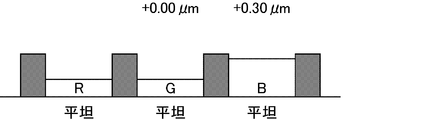
- FIG. 2 is a schematic cross-sectional view of an inkjet color filter substrate according to Embodiment 1.
- FIG. It is a cross-sectional schematic diagram of the color filter substrate in which the colored layer was formed by the photolithography method.
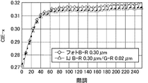
- 6 is a graph showing CIE-x with respect to gradation in the first embodiment.
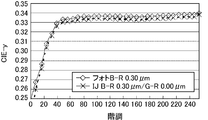
- 6 is a graph showing CIE-y with respect to gradation in the first embodiment.
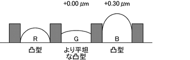
- 6 is a schematic cross-sectional view of an inkjet color filter substrate according to Comparative Example 1.
- FIG. 10 is a graph showing CIE-x with respect to gradation in Comparative Example 1.
- 10 is a graph showing CIE-y with respect to gradation in Comparative Example 1.
- 6 is a schematic cross-sectional view of an inkjet color filter substrate according to Embodiment 2.
- FIG. 6 is a schematic cross-sectional view of an inkjet color filter substrate according to Embodiment 3.
- FIG. 6 is a schematic cross-sectional view of an ink
- the color layer has an uneven shape
- an ink-jet color filter substrate is used as a color filter substrate having a different degree for each color.
- the filter substrate is used, the effect of the present invention can be exhibited as long as the colored layer has unevenness and the color filter substrate has a different degree for each color.
- the color filter substrate of the three primary colors of red (R), green (G), and blue (B) will be described, but the present invention is appropriately applied as long as it is a color filter substrate having a plurality of colored layers. Is possible. Red (R) is also referred to as R, green (G) is also referred to as G, and blue (B) is also referred to as B.
- the film thickness distribution of the “convex” colored layer is 0.3 ⁇ m or more. Preferably, it is 1 ⁇ m or more.
- the “flatter shape” colored layer may have a smaller film thickness distribution than the “uneven” colored layer, but the film thickness distribution is preferably less than 1 ⁇ m. More preferably, it is 0.8 ⁇ m or less.
- the color film thickness of the inkjet color filter substrate was defined by the average film thickness in the pixel.
- the ink-jet color filter substrate has a convex colored layer shape, and has a film thickness distribution unique to the color material of about 1.0 to 2.0 ⁇ m in the pixel.
- the first embodiment is an embodiment in which the color film thickness of G is increased (cell thickness is decreased) when the shape of G is a convex shape that is flatter than the shapes of R and B.
- FIG. 1 is a schematic cross-sectional view of an inkjet color filter substrate according to the first embodiment.
- +0.02 ⁇ m means the height in the G picture element compared to the height (average film thickness) in the R picture element
- +0.30 ⁇ m means the inside of the R picture element.
- the R colored layer and B colored layer described as “convex” are convex compared to the G colored layer described as “flatter convex”.
- the colored layer of G described as “a flatter convex type” is usually a convex type as compared with the colored layer of the photo color filter substrate.
- a relatively flat shape (small difference in unevenness) in the inkjet color filter substrate is referred to as a flatter shape in this specification.
- the color film of the color layer with a good shape (G) is considered in consideration of the color layer shape Ink was ejected by an inkjet method so as to increase the thickness (average film thickness) by 0.02 ⁇ m to form a colored layer. The reason why the color film thickness (average film thickness) of the colored layer of B is increased by 0.30 ⁇ m is as described later.
- the preferred values of the thickness of the R, G, and B colored layers shown in Embodiment 1 are, for example, R; 1.5 to 2.5 ( ⁇ m), G; 1.5 to 2 0.5 ( ⁇ m), B; 1.8 to 2.8 ( ⁇ m).
- the average of the height in the picture element is also referred to as the height (average film thickness) of the colored layer.
- the average film thickness may be an average value of the average film thickness at several points (one or more) in the panel, and an optical shape measuring machine (a surface analysis device [optical interferometer] or the like is particularly preferable) is used. Can be measured. It can also be measured with a step gauge.
- the average film thickness of one picture element is calculated by averaging all the heights included in the picture element, and the measurement is performed by a non-contact type white interferometer or a contact type of a stylus. A step gauge is used. It is preferable to measure in this way.
- the shape of the colored layer varies greatly depending on the ink composition for forming the colored layer and the formation process.
- factors affecting the shape of the colored layer include solid content concentration, pigment concentration, viscosity (at room temperature / heating time), pigment type, dispersion material type, binder type, and solvent type.
- the pigment type, the dispersing material, and the like are usually different depending on the color.
- the factors affecting the shape of the colored layer in the formation process include black matrix shape (taper and height), pre-ink jet base condition (new water repellent condition), ink jet drawing condition (drawing area), and colored layer height. , Ink drying conditions, and ink firing conditions. As long as the colored layer shape is different for each color, the present invention can be suitably applied even if the colored layer shape is different depending on any of the above factors.
- FIG. 2 is a schematic cross-sectional view of a color filter substrate on which a colored layer is formed by photolithography.
- the transmittance of the liquid crystal panel varies depending on the cell thickness, and the optimum value of the cell thickness varies depending on the wavelength of transmitted light. Since the three colors constituting the color filter shown in FIG. 2: R (red), G (green), and B (blue) have different wavelengths for each color, the optimum cell thickness also differs. Since the wavelengths are in the order of B ⁇ G ⁇ R, the cell thickness that minimizes retardation is also B ⁇ G ⁇ R.
- the film thickness should be set in the order of B ⁇ G ⁇ R.
- a sufficient effect can be obtained only by increasing the color film thickness of only B. Therefore, the photo color shown in FIG.
- the filter adopts a structure in which only B has a high color film thickness.
- FIG. 3 is a graph showing CIE-x with respect to gradation in the first embodiment.
- IJB-R 0.30 ⁇ m / GR 0.02 ⁇ m indicates the measurement result of the inkjet color filter substrate shown in FIG.
- Photo BR 0.30 ⁇ m shows the measurement result of the photo color filter substrate shown in FIG.
- the CIE-x value for each gradation of the inkjet color filter substrate is closer to the corresponding value in the photo color filter substrate.
- the gradation chromaticity characteristics of the ink jet color filter substrate are equivalent to the gradation chromaticity characteristics of the photo color filter substrate, and an excellent effect is exhibited.
- FIG. 4 is a graph showing CIE-y with respect to gradation in the first embodiment. As in the case of CIE-x, it can be seen that the gradation chromaticity characteristics of the inkjet color filter substrate are equivalent to the gradation chromaticity characteristics of the photo color filter substrate.
- FIG. 5 is a schematic cross-sectional view of an inkjet color filter substrate according to Comparative Example 1.
- +0.00 ⁇ m means that the height in the G picture element is comparable to the height in the R picture element, and +0.30 ⁇ m means in the R picture element.
- the R colored layer and B colored layer described as “convex” are convex compared to the G colored layer described as “flatter convex”.
- the G colored layer described as “a flatter convex type” is also a convex type as compared with the colored layer of the photo color filter substrate.
- FIG. 6 is a graph showing CIE-x with respect to gradation in Comparative Example 1.
- FIG. 7 is a graph showing CIE-y with respect to gradation in Comparative Example 1.
- the colored layer formed from the G ink used in Embodiment 1 and Comparative Example 1 is compared with the colored layer formed from the R ink and the colored layer formed from the B ink.
- the second embodiment is an embodiment in which the G color film thickness is decreased (cell thickness is increased) when the G shape is a convex shape compared to the R and B shapes.
- FIG. 8 is a schematic cross-sectional view of an inkjet color filter substrate according to the second embodiment.
- “ ⁇ ” means that the height in the G picture element is low compared to the height in the “R” picture element, and “+0.30 ⁇ m” means a comparison with the height in the “R” picture element.
- B means the height in the picture element.
- the G colored layer described as “convex” indicates that it is convex compared to the R colored layer and B colored layer described as “flatter convex”.
- the R colored layer and the B colored layer described as “flatter convex type” are also convex types compared to the colored layer of the photo color filter substrate.
- Embodiment 3 is an embodiment in which the color film thickness of R is increased (cell thickness is decreased) in the case where the shape of R is a convex shape that is flatter than the shapes of G and B.
- FIG. 9 is a schematic cross-sectional view of an inkjet color filter substrate according to the third embodiment.
- “+” means that the height in the R picture element is high compared with the height in the G picture element, and +0.30 ⁇ m means that the height in the G picture element is high.
- B means the height in the picture element.
- the G colored layer and the B colored layer described as “convex” indicate that they are convex compared to the R colored layer described as “flatter convex”. Note that the R colored layer described as “flatter convex type” is also a convex type as compared with the colored layer of the photo color filter substrate.
- Embodiment 4 is an embodiment in which the color film thickness of R is decreased (cell thickness is increased) in the case where the shape of R is convex compared to the shapes of G and B.
- FIG. 10 is a schematic cross-sectional view of an inkjet color filter substrate according to the fourth embodiment.
- ⁇ means that the height in the R picture element is low compared to the height in the G picture element
- +0.30 ⁇ m means that the height in the G picture element is low.
- B means the height in the picture element.
- the R colored layer described as “convex” indicates that it is convex as compared with the G colored layer and B colored layer described as “flatter convex”.
- the G colored layer and the B colored layer described as “flatter convex type” are also convex as compared with the colored layer of the photo color filter substrate.
- the inkjet color filter substrate according to Embodiments 2 to 4 described above can make the gradation chromaticity characteristics equivalent to the gradation chromaticity characteristics of the photo color filter substrate, as in Embodiment 1.
- a liquid crystal display device having excellent display quality can be obtained.
- the blue colored layer has a convex shape or a flatter shape
- the average film thickness is maximized
- the red colored layer has a convex shape so that the average film thickness is thin
- the green colored layer is Form that makes the average film thickness flatter, or the red colored layer has a flatter shape that makes the average film thickness thicker, and the green colored layer has a convex shape that makes the average film thickness thinner
- the form to be shaped is one of the preferred forms in the present invention.
- the present invention can be applied to any of a transmissive liquid crystal display device, a transflective liquid crystal display device, and a reflective liquid crystal display device.
Landscapes
- Physics & Mathematics (AREA)
- Nonlinear Science (AREA)
- General Physics & Mathematics (AREA)
- Optics & Photonics (AREA)
- Engineering & Computer Science (AREA)
- Manufacturing & Machinery (AREA)
- Mathematical Physics (AREA)
- Chemical & Material Sciences (AREA)
- Crystallography & Structural Chemistry (AREA)
- Liquid Crystal (AREA)
- Optical Filters (AREA)
Abstract
本発明は、フォトリソグラフィ法により形成されたカラーフィルタ基板における階調色度特性(カラートラッキング)と同等の階調色度特性を有するカラーフィルタ基板、その製造方法、液晶表示パネル及び液晶表示装置を提供する。本発明のカラーフィルタ基板は、複数色の着色層を有するカラーフィルタ基板であって、上記カラーフィルタ基板は、色ごとに、凹凸を有する着色層と、該凹凸を有する着色層より平坦な形状の着色層とを有し、上記凹凸を有する着色層は、該より平坦な形状の着色層と比べて、平均膜厚が薄いカラーフィルタ基板である。
Description
本発明は、カラーフィルタ基板、その製造方法、液晶表示パネル及び液晶表示装置に関する。より詳しくは、着色層がインクジェット法により形成されたカラーフィルタ基板、その製造方法、液晶表示パネル及び液晶表示装置に関するものである。
表示パネルは、様々な方式のパネルが実用化されてモバイルディスプレイパネルから大型ディスプレイパネルまで多くの製品が供給されている。中でも液晶表示パネルは、一対の基板間に液晶表示素子を挟持して構成され、基板に形成した電極により液晶層に電圧を印加して液晶層の配向状態を変化させることによって光の偏光状態を変化させて表示を行うものであり、薄型で軽量かつ低消費電力といった特長を活かして、モバイル用途や各種のモニター、テレビ等、日常生活やビジネスに欠かすことのできないものとなっている。近年においては、電子ブック、フォトフレーム、IA(産業機器)、PC(パーソナルコンピュータ)用途等に幅広く採用されている。
この液晶表示パネルでは、カラー表示を行うために、一対の基板の一方を構成するカラーフィルタ基板に複数色の着色層(カラーフィルタ)が形成されたものである。カラーフィルタ基板は、一般的に、複数色の着色層が表示領域の全体に規則正しく配置されたものである。カラー表示を実現するための最小単位である画素を構成する着色層の色の組み合わせとしては、例えば、赤(R)、青(B)、緑(G)からなる基本3原色又はそれよりも多くの色単位を含んで1つの画素が構成されたものが挙げられる。
従来の液晶表示パネルにおける着色層の形成方法としては、フォトリソグラフィ法、インクジェット法等が挙げられ、現在、いずれの方法も多く用いられている。
ここで、カラーフィルタにおける膜厚・インクの管理や決定方法としては、特定の一成分又は特定の2種類以上の成分を特定の量比で組み合わせた成分群および1種類のみ又は特定の量比で組み合わせた2種類以上の他の成分からなる所定の基本組成を基準とするインク系列を評価対象として設定し、当該基本組成中の前記特定の一成分又は成分群と他の成分との量比を変えることで、当該特定の一成分又は成分群の含有量が異なるインクを2種類以上準備する工程、前記各インクをインクジェット方式で基板上に塗布して画素を形成し、当該画素の平均膜厚を測定し、さらに当該画素の分光測定をその測定領域の面積を画素開口部の面積よりも大きくして行うことで、各インクごとに目標とする色度座標を有する画素の平均膜厚を特定する工程、前記各インクごとに目標とする色度座標を有する画素の平均膜厚を特定した結果に基づいて、これらのインクが属するインク系列において、前記特定の成分又は成分群の含有量と、目標とする色度座標を達成できる前記画素の平均膜厚との関係を特定する工程、及び、前記インクについて特定された前記関係に基づいて、当該インク系列に属するインクの中から所定の平均膜厚において前記目標とする色度座標を達成できるインクの組成を決定する工程、を含むことを特徴とする、カラーフィルタの画素を形成するためのインクジェット方式用インクの評価方法が開示されている(例えば、特許文献1参照。)。
しかしながら、上記特許文献には、膜厚・インクの管理や決定方法が記載されているだけであり、着色層における色ごとの膜厚段差調整には何ら言及していない。
上述したように、着色層の形成方法としては、フォトリソグラフィ法、インクジェット法等が挙げられ、現在、いずれの方法も多く用いられている。このことから、表示パネル同一機種に対し、フォトリソグラフィ法により形成されたカラーフィルタ基板(以下、フォトカラーフィルタ基板ともいう。)と、インクジェット法により形成されたカラーフィルタ基板(以下、インクジェットカラーフィルタ基板ともいう。)とを含んだ複数種類のカラーフィルタを採用しなければならない場合が頻繁に生じる。したがって、フォトカラーフィルタ基板と、インクジェットカラーフィルタ基板との間に光学的な面での互換性があることが重要であった。中でも、フォトカラーフィルタ基板と、インクジェットカラーフィルタ基板との間で階調色度特性が同等であることが、液晶表示パネルを工業的に製造する際に、製品によって表示にムラが生じることを防ぐために強く望まれるところである。
しかしながら、従来のカラーフィルタ基板においては、階調色度特性(カラートラッキング)をフォトカラーフィルタ基板とインクジェットカラーフィルタ基板との間で同等のものとするための工夫の余地があった。
本発明は、上記現状に鑑みてなされたものであり、フォトリソグラフィ法により形成されたカラーフィルタ基板における階調色度特性(カラートラッキング)と同等の階調色度特性を有するカラーフィルタ基板、その製造方法、液晶表示パネル及び液晶表示装置を提供することを目的とするものである。
本発明者は、フォトカラーフィルタ基板における階調色度特性と同等の階調色度特性を有するカラーフィルタ基板、液晶表示パネル及び液晶表示装置について種々検討したところ、インクジェットカラーフィルタ基板等のカラーフィルタ基板においては、着色層が凹凸を有すること、色ごとにその程度が相違することに着目した。そして、着色層が凹凸を有し、色ごとにその程度が相違するために、フォトカラーフィルタ基板のように着色層の形状が一定(平坦)なカラーフィルタ基板と階調色度特性を充分に合わせることができないことを見いだすとともに、色ごとの膜厚段差調整を行い、液晶表示パネルにおける各色ごとのセルギャップ(一対の基板間の間隔)を適当なものに調整することにより、上記インクジェットカラーフィルタ基板等のカラーフィルタ基板においても上記フォトカラーフィルタ基板等のカラーフィルタ基板における階調色度特性と同等の階調色度特性を得ることができることを見いだし、上記課題をみごとに解決することができることに想到し、本発明に到達したものである。
すなわち、本発明は、複数色の着色層を有するカラーフィルタ基板であって、上記カラーフィルタ基板は、色ごとに、凹凸を有する着色層と、該凹凸を有する着色層より平坦な形状の(より凹凸差の小さい)着色層とを有し、上記凹凸を有する着色層は、該より平坦な形状の着色層と比べて、平均膜厚が薄いカラーフィルタ基板である。
上記凹凸を有する着色層とは、カラーフィルタ基板を断面視したときに平坦ではないものであればよく、凹部又は凸部のいずれかを有するものであればよい。
上記凹凸を有する着色層は、該より平坦な形状の着色層と比べて、平均膜厚が薄いとは、本発明のカラーフィルタ基板の技術分野において薄いといえるものであればよいが、例えば、0.01μm以上、0.05μm以下だけ薄いことが好ましい。より好ましい下限値は、0.015μmである。また、より好ましい上限値は、0.03μmである。
上記凹凸を有する着色層は、凸型形状であることが好ましい。凸型形状とは、通常、インクジェット法等によって、インクがカラーフィルタ基板上のバンクとバンクとの間に吐出された場合に、当該カラーフィルタ基板に対して反対側に向かって、表面張力によって凸状に形成される形状をいう。
なお、凹凸を有する着色層と、該凹凸を有する着色層より平坦な形状の着色層(本明細書中、単により平坦な形状の着色層ともいう。)とを有するとは、例えば、カラーフィルタ基板上で複数色の着色層によって一組の色表示単位を構成し、凹凸の度合いが異なる着色層によって各色の着色層が構成される場合、凹凸の度合いが高い着色層を、凹凸を有する着色層とし、凹凸の度合いが最も低い着色層を、該より平坦な形状の着色層とすればよい。すなわち、断面形状において、カラーフィルタ基板に対して反対側の着色層の上辺がカラーフィルタ基板の主面に対して最も沿っている(最も平行である)形状を凹凸の度合いが最も低いとし、該上辺がカラーフィルタ基板に対して反対側に盛り上がって湾曲した形状を凸形状とし、該上辺がカラーフィルタ基板に対してカラーフィルタ基板側に盛り下がって湾曲した形状を凹形状とし、湾曲の度合いが大きい着色層と小さい着色層とによって各色の着色層が構成される場合には、湾曲の度合いが大きい着色層を、凹凸を有する着色層とし、湾曲の度合いが最も低い着色層又は該上辺がカラーフィルタ基板に対して略平行である着色層を、該より平坦な形状の着色層とすればよい。凹凸を有する着色層及び該より平坦な形状の着色層は、それぞれ、1つの画素内に1つであってもよく、複数であってもよい。
上記着色層は、インクジェット法により形成されたものであることが好ましい。これによって、工程の少ない方法により簡便にカラーフィルタ基板を作製することができる。なお、インクがカラーフィルタ基板上のバンクとバンクとの間に吐出されて表面張力により着色層に凹凸形状を与えることになるが、これによって生じる課題は、本願発明により解消することができる。
上記凹凸を有する着色層は、1つの絵素の1色の着色層における膜厚分布が0.3μm以上であることが好ましい。より好ましくは、1μm以上である。また、3μm以下であることが好ましい。
なお、着色層の膜厚とは、着色層におけるカラーフィルタ基板側の下辺から上辺の最高点までの長さである。すなわち、着色層におけるカラーフィルタ基板側の下辺から上辺にかけて該基板主面に対して垂線を引いたときに、該垂線が下辺と交わる点から上辺と交わる点との間の長さのうち、最も長いものを着色層の膜厚とする。また、膜厚分布とは、本明細書中、一つの着色層(1絵素中の、1色の着色層)の中での膜厚の最短から最長までの範囲をいう。
上記より平坦な形状の着色層は、凹凸を有する着色層よりも当該膜厚分布が小さいものであればよいが、膜厚分布が0μm以上、1μm未満であることが好ましい。上記のような範囲内とすることにより、上述したように階調色度特性を合わせることができると共に、着色層の膜厚分布のバラツキによる表示品位への影響を抑制することができる。
なお、着色層の膜厚とは、着色層におけるカラーフィルタ基板側の下辺から上辺の最高点までの長さである。すなわち、着色層におけるカラーフィルタ基板側の下辺から上辺にかけて該基板主面に対して垂線を引いたときに、該垂線が下辺と交わる点から上辺と交わる点との間の長さのうち、最も長いものを着色層の膜厚とする。また、膜厚分布とは、本明細書中、一つの着色層(1絵素中の、1色の着色層)の中での膜厚の最短から最長までの範囲をいう。
上記より平坦な形状の着色層は、凹凸を有する着色層よりも当該膜厚分布が小さいものであればよいが、膜厚分布が0μm以上、1μm未満であることが好ましい。上記のような範囲内とすることにより、上述したように階調色度特性を合わせることができると共に、着色層の膜厚分布のバラツキによる表示品位への影響を抑制することができる。
本発明はまた、複数色の着色層を有するカラーフィルタ基板の製造方法であって、上記製造方法は、色ごとに、凹凸を有する着色層と、該凹凸を有する着色層より平坦な形状の着色層とを形成し、上記凹凸を有する着色層は、該より平坦な形状の着色層と比べて、平均膜厚が薄いカラーフィルタ基板の製造方法でもある。
本発明のカラーフィルタ基板の製造方法は、上記本発明のカラーフィルタ基板と同様に、上記凹凸を有する着色層が凸型形状であることが好ましく、上記着色層をインクジェット法により形成することが好ましい。上記着色層をインクジェット法により形成する場合、カラーフィルタ基板の通常の製造工程中にインクジェット法による着色層形成工程を含め、当該工程において、上記のように凹凸を有する着色層と、該凹凸を有する着色層より平坦な形状の着色層とを有する形態とが調製されるようにすればよい。
本発明はまた、本発明のカラーフィルタ基板、又は、本発明のカラーフィルタ基板の製造方法により得られたカラーフィルタ基板を備える液晶表示パネルでもある。
本発明の液晶表示パネルは、例えば、本発明のカラーフィルタ基板と、回路基板等の基板との一対の基板により、液晶層を挟持してなるものとすることができる。該一対の基板の少なくとも一方は、液晶層と反対側に、偏光板を有するものとすることができる。上記回路基板は、例えば、TFTアレイ基板とすることができる。
本発明の液晶表示パネルは、例えば、本発明のカラーフィルタ基板と、回路基板等の基板との一対の基板により、液晶層を挟持してなるものとすることができる。該一対の基板の少なくとも一方は、液晶層と反対側に、偏光板を有するものとすることができる。上記回路基板は、例えば、TFTアレイ基板とすることができる。
本発明は更に、本発明の液晶表示パネルを備える液晶表示装置でもある。
上記液晶表示装置とは、上記液晶表示パネルを備え、表示装置として必要な装置等を備えたものやその他の機能を有する装置等を備えたものであればよい。例えば、テレビ、電子ブック、PC(パーソナルコンピュータ)、フォトフレーム等、大型テレビ等の大画面表示装置からモバイル用途における表示装置まで幅広く適用することができる。
上記液晶表示装置とは、上記液晶表示パネルを備え、表示装置として必要な装置等を備えたものやその他の機能を有する装置等を備えたものであればよい。例えば、テレビ、電子ブック、PC(パーソナルコンピュータ)、フォトフレーム等、大型テレビ等の大画面表示装置からモバイル用途における表示装置まで幅広く適用することができる。
本発明のカラーフィルタ基板の製造方法、本発明の液晶表示パネルが備えるカラーフィルタ基板、及び、本発明の液晶表示装置が備えるカラーフィルタ基板の好ましい形態としては、本発明のカラーフィルタ基板の好ましい形態を適宜適用することができる。また、本発明の液晶表示装置が備える液晶表示パネルにおいては、本発明の液晶表示パネルの好ましい形態を適宜適用することができる。
本発明のカラーフィルタ基板、液晶表示パネル及び液晶表示装置の構成としては、このような構成要素を必須として形成されるものである限り、その他の構成要素により特に限定されるものではなく、カラーフィルタ基板、液晶表示パネル及び液晶表示装置に通常用いられるその他の構成を適宜適用することができる。
上述した各形態は、本発明の要旨を逸脱しない範囲において適宜組み合わされてもよい。
本発明のカラーフィルタ基板、液晶表示パネル及び液晶表示装置によれば、着色層の形状が凸型となっており、色ごとにその程度が相違するカラーフィルタ基板においても、着色層の形状が一定なカラーフィルタ基板と階調色度特性を充分に合わせることができる。
以下に実施形態を掲げ、本発明を図面を参照して更に詳細に説明するが、本発明はこれらの実施形態のみに限定されるものではない。また、以下の実施形態では、着色層の形状が凹凸を有し、色ごとにその程度が異なるカラーフィルタ基板としてインクジェットカラーフィルタ基板を用い、着色層の形状が一定であるカラーフィルタ基板としてフォトカラーフィルタ基板を用いているが、着色層が凹凸を有し、色ごとにその程度が異なるカラーフィルタ基板である限り、本願発明の効果を発揮することができる。以下では、赤(R)、緑(G)、青(B)の3原色のカラーフィルタ基板等について述べるが、複数色の着色層を有するカラーフィルタ基板である限り、本発明を適宜適用することが可能である。また、赤(R)は、Rともいい、緑(G)は、Gともいい、青(B)は、Bともいう。
本明細書中、「より平坦」とは、着色層の凹型形状及び/又は凸型形状による膜厚分布がより小さいことをいう。また、以下の実施形態では、「凸型」の着色層は、その膜厚分布が0.3μm以上である。好ましくは、1μm以上である。また、「より平坦な形状」の着色層は、「凹凸を有する」着色層よりも膜厚分布が小さいものであればよいが、膜厚分布が1μm未満であることが好適である。より好ましくは、0.8μm以下である。
またインクジェットカラーフィルタ基板の色膜厚は画素内平均膜厚にて規定した。インクジェットカラーフィルタ基板は、着色層形状が凸型になっており、画素内に1.0~2.0μm程度の色材固有の膜厚分布がある。
実施形態1
実施形態1は、Gの形状がR、Bの形状に比較してより平坦な凸型である場合において、Gの色膜厚を上げる(セル厚を下げる)場合の実施形態である。
図1は、実施形態1に係るインクジェットカラーフィルタ基板の断面模式図である。図1中、+0.02μmとは、Rの絵素内の高さ(平均膜厚)と比較した、Gの絵素内の高さを意味し、+0.30μmとは、Rの絵素内の高さと比較した、Bの絵素内の高さを意味する。「凸型」と記載されたRの着色層及びBの着色層は、「より平坦な凸型」と記載されたGの着色層と比較して凸型であることを示す。なお、「より平坦な凸型」と記載されたGの着色層も、通常は、フォトカラーフィルタ基板の着色層と比較すると凸型となっている。しかしながら、このようにインクジェットカラーフィルタ基板において相対的に平坦な(凹凸差の小さい)形状を、本明細書中、より平坦な形状という。
実施形態1では、このように、インクジェットカラーフィルタ基板についてフォトカラーフィルタ基板と階調色度特性を同等に仕上げるため、着色層形状を考慮し、形状の良い色(G)の着色層の色膜厚(平均膜厚)を0.02μm上げるようにインクジェット法によりインクを吐出して、着色層を形成した。なお、Bの着色層の色膜厚(平均膜厚)を0.30μm上げる理由は、後述する通りである。
実施形態1は、Gの形状がR、Bの形状に比較してより平坦な凸型である場合において、Gの色膜厚を上げる(セル厚を下げる)場合の実施形態である。
図1は、実施形態1に係るインクジェットカラーフィルタ基板の断面模式図である。図1中、+0.02μmとは、Rの絵素内の高さ(平均膜厚)と比較した、Gの絵素内の高さを意味し、+0.30μmとは、Rの絵素内の高さと比較した、Bの絵素内の高さを意味する。「凸型」と記載されたRの着色層及びBの着色層は、「より平坦な凸型」と記載されたGの着色層と比較して凸型であることを示す。なお、「より平坦な凸型」と記載されたGの着色層も、通常は、フォトカラーフィルタ基板の着色層と比較すると凸型となっている。しかしながら、このようにインクジェットカラーフィルタ基板において相対的に平坦な(凹凸差の小さい)形状を、本明細書中、より平坦な形状という。
実施形態1では、このように、インクジェットカラーフィルタ基板についてフォトカラーフィルタ基板と階調色度特性を同等に仕上げるため、着色層形状を考慮し、形状の良い色(G)の着色層の色膜厚(平均膜厚)を0.02μm上げるようにインクジェット法によりインクを吐出して、着色層を形成した。なお、Bの着色層の色膜厚(平均膜厚)を0.30μm上げる理由は、後述する通りである。
なお、実施形態1において示された好適なR、G、Bの着色層自体の膜厚の値としては、例えば、R;1.5~2.5(μm)、G;1.5~2.5(μm)、B;1.8~2.8(μm)となる。
本明細書中、絵素内の高さを平均化したものを、着色層の高さ(平均膜厚)ともいう。以下の実施形態においても同様である。平均膜厚は、パネル内の数点(1個以上)の平均膜厚の平均値であればよく、光学系の形状測定機(表面解析装置〔光学干渉計〕等が特に好ましい。)を使用して測定することができる。また、段差計でも測定可能である。本実施形態では、1絵素の平均膜厚は、絵素内に含まれる全ての高さを平均して算出しており、測定は、非接触型白色干渉計、又は、触針の接触型段差計を使用している。このようにして測定することが好適である。
なお、インクジェットカラーフィルタ基板等のカラーフィルタ基板においては、着色層の形状は、着色層を形成するためのインク組成と形成プロセスで大きく変化する。
インク組成について、着色層形状へ影響を与えるファクターとしては、固形分濃度、顔料濃度、粘度(常温時・加熱時)、顔料種、分散材種、バインダー種、溶媒種が挙げられる。
なお、元来、色により顔料種・分散材等が異なることが通常である。
インク組成について、着色層形状へ影響を与えるファクターとしては、固形分濃度、顔料濃度、粘度(常温時・加熱時)、顔料種、分散材種、バインダー種、溶媒種が挙げられる。
なお、元来、色により顔料種・分散材等が異なることが通常である。
また、形成プロセスについて、着色層形状へ影響を与えるファクターとしては、ブラックマトリクス形状(テーパーや高さ)、インクジェット前下地条件(新撥水条件)、インクジェット描画条件(描画エリア)、着色層高さ、インク乾燥条件、インク焼成条件が挙げられる。
本発明は、着色層形状が色ごとに相違するものである限り、上記のいずれのファクターによって着色層形状が相違するものであっても、好適に適用することができる。
本発明は、着色層形状が色ごとに相違するものである限り、上記のいずれのファクターによって着色層形状が相違するものであっても、好適に適用することができる。
図2は、フォトリソグラフィ法により着色層が形成されたカラーフィルタ基板の断面模式図である。図2においては、いずれの着色層も平坦となっており、GとRとは、同じ厚さに設定されている(G-R=+0.00μm)。なお、図2に示したフォトカラーフィルタ基板は、図1に示したインクジェットカラーフィルタ基板と同様に、Bが非常に厚く設定されている(B-R=+0.30μm)。この理由としては、以下の通りである。
液晶パネルの透過率はセル厚によって変化し、そのセル厚の最適値は、透過する光の波長により異なる。図2に示したカラーフィルタを構成する3色:R(赤)、G(緑)、B(青)は、各色で波長が異なるため、最適となるセル厚も異なる。波長がB<G<Rの順となるため、リタデーションの最小となるセル厚もB<G<Rとなる。
このように色膜厚を最適値に設定すると、液晶パネル点灯時の不要な色付きが軽減したり、白の透過率が改善されるなどの効果が得られる。そのため、本来はB<G<Rの順に膜厚を設定すべきであるが、上記したようにBのみの色膜厚を上げるだけで充分な効果が得られるため、図2に示したフォトカラーフィルタは、Bのみ色膜厚が高い構造を採用している。
図3は、実施形態1における階調に対するCIE-xを示すグラフである。図3中、IJB-R 0.30μm/G-R 0.02μmは、図1に示したインクジェットカラーフィルタ基板についての測定結果を示す。フォトB-R 0.30μmは、図2に示したフォトカラーフィルタ基板についての測定結果を示す。
後述する比較例1と比較して、インクジェットカラーフィルタ基板の各階調ごとのCIE-xの値(特に、低階調におけるCIE-xの値)がフォトカラーフィルタ基板における対応する値に近くなっており、インクジェットカラーフィルタ基板の階調色度特性がフォトカラーフィルタ基板の階調色度特性が同等となっており、優れた効果を発揮していることが分かる。
後述する比較例1と比較して、インクジェットカラーフィルタ基板の各階調ごとのCIE-xの値(特に、低階調におけるCIE-xの値)がフォトカラーフィルタ基板における対応する値に近くなっており、インクジェットカラーフィルタ基板の階調色度特性がフォトカラーフィルタ基板の階調色度特性が同等となっており、優れた効果を発揮していることが分かる。
図4は、実施形態1における階調に対するCIE-yを示すグラフである。CIE-xの場合と同様に、インクジェットカラーフィルタ基板の階調色度特性がフォトカラーフィルタ基板の階調色度特性と同等となっていることが分かる。
比較例1
図5は、比較例1に係るインクジェットカラーフィルタ基板の断面模式図である。図5中、+0.00μmとは、Rの絵素内の高さと比較した、Gの絵素内の高さが同程度であることを意味し、+0.30μmとは、Rの絵素内の高さと比較した、Bの絵素内の高さを意味する。「凸型」と記載されたRの着色層及びBの着色層は、「より平坦な凸型」と記載されたGの着色層と比較して凸型であることを示す。なお、「より平坦な凸型」と記載されたGの着色層も、フォトカラーフィルタ基板の着色層と比較すると凸型となっている。
すなわち、比較例1は、インクジェットカラーフィルタ基板について、フォトカラーフィルタの設計値通り、色膜厚段差B-RG=+0.30μmと設定し、パネル作製を行ったものであり、着色層形状を考慮して、着色層の色膜厚(平均膜厚)を調整していないものである。
図5は、比較例1に係るインクジェットカラーフィルタ基板の断面模式図である。図5中、+0.00μmとは、Rの絵素内の高さと比較した、Gの絵素内の高さが同程度であることを意味し、+0.30μmとは、Rの絵素内の高さと比較した、Bの絵素内の高さを意味する。「凸型」と記載されたRの着色層及びBの着色層は、「より平坦な凸型」と記載されたGの着色層と比較して凸型であることを示す。なお、「より平坦な凸型」と記載されたGの着色層も、フォトカラーフィルタ基板の着色層と比較すると凸型となっている。
すなわち、比較例1は、インクジェットカラーフィルタ基板について、フォトカラーフィルタの設計値通り、色膜厚段差B-RG=+0.30μmと設定し、パネル作製を行ったものであり、着色層形状を考慮して、着色層の色膜厚(平均膜厚)を調整していないものである。
図6は、比較例1における階調に対するCIE-xを示すグラフである。
図7は、比較例1における階調に対するCIE-yを示すグラフである。
光学特性評価の結果、低階調領域の色度(特に、CIE-x)がフォトカラーフィルタ基板と比較して、異なる階調色度特性を持つことが分かった。着色層の凸型形状が色により異なるため、全色フラットであるフォトカラーフィルタ基板とはパネル特性が異なることと考えられる。このようなインクジェットカラーフィルタ基板は、フォトカラーフィルタとの互換性を充分に満足できないこととなる。
図7は、比較例1における階調に対するCIE-yを示すグラフである。
光学特性評価の結果、低階調領域の色度(特に、CIE-x)がフォトカラーフィルタ基板と比較して、異なる階調色度特性を持つことが分かった。着色層の凸型形状が色により異なるため、全色フラットであるフォトカラーフィルタ基板とはパネル特性が異なることと考えられる。このようなインクジェットカラーフィルタ基板は、フォトカラーフィルタとの互換性を充分に満足できないこととなる。
実施形態1及び比較例1において使用したG用のインクから形成された着色層は、R用のインクから形成された着色層、B用のインクから形成された着色層に比較し、画素内の膜厚分布が狭い傾向があった(より平坦な形状であった)。
そのため、R、Bに比べ、Gの実効セル厚や配向のタイミングが異なり、低階調領域でのG輝度がRBのそれよりも高く、フォトカラーフィルタ基板と比べて白での低階調色度にズレが生じたことが考えられる。
今回、比較例1に示したように、低階調にてインクジェット品は色度CIE-x、CIE-y(特に、CIE-x)が低い方に推移し、見た目に緑~青味がかる傾向にあった。そこで、形状の差異を考慮し、実施形態1に示したように、B-R=+0.30μm/G-R=+0.02μmに設定した。
そのため、R、Bに比べ、Gの実効セル厚や配向のタイミングが異なり、低階調領域でのG輝度がRBのそれよりも高く、フォトカラーフィルタ基板と比べて白での低階調色度にズレが生じたことが考えられる。
今回、比較例1に示したように、低階調にてインクジェット品は色度CIE-x、CIE-y(特に、CIE-x)が低い方に推移し、見た目に緑~青味がかる傾向にあった。そこで、形状の差異を考慮し、実施形態1に示したように、B-R=+0.30μm/G-R=+0.02μmに設定した。
これにより、より互換性の高いカラーフィルタ基板を工程数の少ないインクジェットにて作製することが可能になる。
実施形態2
実施形態2は、Gの形状がR、Bの形状に比較して凸型の場合において、Gの色膜厚を下げる(セル厚を上げる)場合の実施形態である。
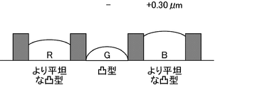
図8は、実施形態2に係るインクジェットカラーフィルタ基板の断面模式図である。図8中、-とは、Rの絵素内の高さと比較した、Gの絵素内の高さが低いことを意味し、+0.30μmとは、Rの絵素内の高さと比較した、Bの絵素内の高さを意味する。「凸型」と記載されたGの着色層は、「より平坦な凸型」と記載されたRの着色層及びBの着色層と比較して凸型であることを示す。なお、「より平坦な凸型」と記載されたRの着色層及びBの着色層も、フォトカラーフィルタ基板の着色層と比較すると凸型となっている。
実施形態2は、Gの形状がR、Bの形状に比較して凸型の場合において、Gの色膜厚を下げる(セル厚を上げる)場合の実施形態である。
図8は、実施形態2に係るインクジェットカラーフィルタ基板の断面模式図である。図8中、-とは、Rの絵素内の高さと比較した、Gの絵素内の高さが低いことを意味し、+0.30μmとは、Rの絵素内の高さと比較した、Bの絵素内の高さを意味する。「凸型」と記載されたGの着色層は、「より平坦な凸型」と記載されたRの着色層及びBの着色層と比較して凸型であることを示す。なお、「より平坦な凸型」と記載されたRの着色層及びBの着色層も、フォトカラーフィルタ基板の着色層と比較すると凸型となっている。
実施形態3
実施形態3は、Rの形状がG、Bの形状に比較してより平坦な凸型である場合において、Rの色膜厚を上げる(セル厚を下げる)場合の実施形態である。
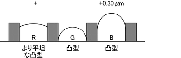
図9は、実施形態3に係るインクジェットカラーフィルタ基板の断面模式図である。図9中、+とは、Gの絵素内の高さと比較した、Rの絵素内の高さが高いことを意味し、+0.30μmとは、Gの絵素内の高さと比較した、Bの絵素内の高さを意味する。「凸型」と記載されたGの着色層及びBの着色層は、「より平坦な凸型」と記載されたRの着色層と比較して凸型であることを示す。なお、「より平坦な凸型」と記載されたRの着色層も、フォトカラーフィルタ基板の着色層と比較すると凸型となっている。
実施形態3は、Rの形状がG、Bの形状に比較してより平坦な凸型である場合において、Rの色膜厚を上げる(セル厚を下げる)場合の実施形態である。
図9は、実施形態3に係るインクジェットカラーフィルタ基板の断面模式図である。図9中、+とは、Gの絵素内の高さと比較した、Rの絵素内の高さが高いことを意味し、+0.30μmとは、Gの絵素内の高さと比較した、Bの絵素内の高さを意味する。「凸型」と記載されたGの着色層及びBの着色層は、「より平坦な凸型」と記載されたRの着色層と比較して凸型であることを示す。なお、「より平坦な凸型」と記載されたRの着色層も、フォトカラーフィルタ基板の着色層と比較すると凸型となっている。
実施形態4
実施形態4は、Rの形状がG、Bの形状に比較して凸型の場合において、Rの色膜厚を下げる(セル厚を上げる)場合の実施形態である。
図10は、実施形態4に係るインクジェットカラーフィルタ基板の断面模式図である。図10中、-とは、Gの絵素内の高さと比較した、Rの絵素内の高さが低いことを意味し、+0.30μmとは、Gの絵素内の高さと比較した、Bの絵素内の高さを意味する。「凸型」と記載されたRの着色層は、「より平坦な凸型」と記載されたGの着色層及びBの着色層と比較して凸型であることを示す。なお、「より平坦な凸型」と記載されたGの着色層及びBの着色層も、フォトカラーフィルタ基板の着色層と比較すると凸型となっている。
上述した実施形態2~4に係るインクジェットカラーフィルタ基板は、実施形態1と同様に、その階調色度特性をフォトカラーフィルタ基板の階調色度特性と同等とすることができるものである。本実施形態のインクジェットカラーフィルタ又は本実施形態のインクジェットカラーフィルタを備えた液晶表示パネルにより、表示品位に優れた液晶表示装置を得ることが可能である。例えば、青色の着色層を凸型形状又はより平坦な形状とし、平均膜厚を最も大きくしたうえで、赤色の着色層を平均膜厚が薄くなるように凸型形状とし、緑色の着色層を平均膜厚が厚くなるようにより平坦な形状とする形態、又は、赤色の着色層を平均膜厚が厚くなるようにより平坦な形状とし、緑色の着色層を平均膜厚が薄くなるように凸型形状とする形態が、本発明における好ましい形態の1つである。
実施形態4は、Rの形状がG、Bの形状に比較して凸型の場合において、Rの色膜厚を下げる(セル厚を上げる)場合の実施形態である。
図10は、実施形態4に係るインクジェットカラーフィルタ基板の断面模式図である。図10中、-とは、Gの絵素内の高さと比較した、Rの絵素内の高さが低いことを意味し、+0.30μmとは、Gの絵素内の高さと比較した、Bの絵素内の高さを意味する。「凸型」と記載されたRの着色層は、「より平坦な凸型」と記載されたGの着色層及びBの着色層と比較して凸型であることを示す。なお、「より平坦な凸型」と記載されたGの着色層及びBの着色層も、フォトカラーフィルタ基板の着色層と比較すると凸型となっている。
上述した実施形態2~4に係るインクジェットカラーフィルタ基板は、実施形態1と同様に、その階調色度特性をフォトカラーフィルタ基板の階調色度特性と同等とすることができるものである。本実施形態のインクジェットカラーフィルタ又は本実施形態のインクジェットカラーフィルタを備えた液晶表示パネルにより、表示品位に優れた液晶表示装置を得ることが可能である。例えば、青色の着色層を凸型形状又はより平坦な形状とし、平均膜厚を最も大きくしたうえで、赤色の着色層を平均膜厚が薄くなるように凸型形状とし、緑色の着色層を平均膜厚が厚くなるようにより平坦な形状とする形態、又は、赤色の着色層を平均膜厚が厚くなるようにより平坦な形状とし、緑色の着色層を平均膜厚が薄くなるように凸型形状とする形態が、本発明における好ましい形態の1つである。
なお、本発明は、透過型の液晶表示装置、半透過型の液晶表示装置、反射型の液晶表示装置のいずれにも適用可能である。
上述した実施形態における各形態は、本発明の要旨を逸脱しない範囲において適宜組み合わされてもよい。
なお、本願は、2010年11月16日に出願された日本国特許出願2010-256239号を基礎として、パリ条約ないし移行する国における法規に基づく優先権を主張するものである。該出願の内容は、その全体が本願中に参照として組み込まれている。
Claims (8)
- 複数色の着色層を有するカラーフィルタ基板であって、
該カラーフィルタ基板は、色ごとに、凹凸を有する着色層と、該凹凸を有する着色層より平坦な形状の着色層とを有し、
該凹凸を有する着色層は、該より平坦な形状の着色層と比べて、平均膜厚が薄い
ことを特徴とするカラーフィルタ基板。 - 前記凹凸を有する着色層は、凸型形状である
ことを特徴とする請求項1に記載のカラーフィルタ基板。 - 前記着色層は、インクジェット法により形成されたものである
ことを特徴とする請求項1又は2に記載のカラーフィルタ基板。 - 複数色の着色層を有するカラーフィルタ基板の製造方法であって、
該製造方法は、色ごとに、凹凸を有する着色層と、該凹凸を有する着色層より平坦な形状の着色層とを形成し、
該凹凸を有する着色層は、該より平坦な形状の着色層と比べて、平均膜厚が薄い
ことを特徴とするカラーフィルタ基板の製造方法。 - 前記凹凸を有する着色層は、凸型形状である
ことを特徴とする請求項4に記載のカラーフィルタ基板の製造方法。 - 前記着色層は、インクジェット法により形成する
ことを特徴とする請求項4又は5に記載のカラーフィルタ基板の製造方法。 - 請求項1~3のいずれかに記載のカラーフィルタ基板、又は、請求項4~6のいずれかに記載のカラーフィルタ基板の製造方法により得られたカラーフィルタ基板を備えることを特徴とする液晶表示パネル。
- 請求項7に記載の液晶表示パネルを備えることを特徴とする液晶表示装置。
Applications Claiming Priority (2)
| Application Number | Priority Date | Filing Date | Title |
|---|---|---|---|
| JP2010256239 | 2010-11-16 | ||
| JP2010-256239 | 2010-11-16 |
Publications (1)
| Publication Number | Publication Date |
|---|---|
| WO2012066971A1 true WO2012066971A1 (ja) | 2012-05-24 |
Family
ID=46083905
Family Applications (1)
| Application Number | Title | Priority Date | Filing Date |
|---|---|---|---|
| PCT/JP2011/075654 Ceased WO2012066971A1 (ja) | 2010-11-16 | 2011-11-08 | カラーフィルタ基板、その製造方法、液晶表示パネル及び液晶表示装置 |
Country Status (1)
| Country | Link |
|---|---|
| WO (1) | WO2012066971A1 (ja) |
Citations (5)
| Publication number | Priority date | Publication date | Assignee | Title |
|---|---|---|---|---|
| JPH06130218A (ja) * | 1992-10-20 | 1994-05-13 | Toshiba Corp | カラ−フィルタおよび液晶表示装置 |
| JPH07325299A (ja) * | 1994-06-01 | 1995-12-12 | Toppan Printing Co Ltd | 液晶表示装置用カラーフィルター |
| JPH0949915A (ja) * | 1995-08-04 | 1997-02-18 | Hitachi Chem Co Ltd | カラーフィルタの製造法 |
| JP2005005419A (ja) * | 2003-06-11 | 2005-01-06 | Toppan Printing Co Ltd | 固体撮像素子 |
| JP2009237437A (ja) * | 2008-03-28 | 2009-10-15 | Toray Ind Inc | 半透過型液晶表示装置用カラーフィルタ基板の製造方法、およびこれを用いた半透過型液晶表示装置 |
-
2011
- 2011-11-08 WO PCT/JP2011/075654 patent/WO2012066971A1/ja not_active Ceased
Patent Citations (5)
| Publication number | Priority date | Publication date | Assignee | Title |
|---|---|---|---|---|
| JPH06130218A (ja) * | 1992-10-20 | 1994-05-13 | Toshiba Corp | カラ−フィルタおよび液晶表示装置 |
| JPH07325299A (ja) * | 1994-06-01 | 1995-12-12 | Toppan Printing Co Ltd | 液晶表示装置用カラーフィルター |
| JPH0949915A (ja) * | 1995-08-04 | 1997-02-18 | Hitachi Chem Co Ltd | カラーフィルタの製造法 |
| JP2005005419A (ja) * | 2003-06-11 | 2005-01-06 | Toppan Printing Co Ltd | 固体撮像素子 |
| JP2009237437A (ja) * | 2008-03-28 | 2009-10-15 | Toray Ind Inc | 半透過型液晶表示装置用カラーフィルタ基板の製造方法、およびこれを用いた半透過型液晶表示装置 |
Similar Documents
| Publication | Publication Date | Title |
|---|---|---|
| US11215865B2 (en) | Color filter substrate, manufacturing method thereof, and related devices | |
| US6738204B1 (en) | Arrangement of color elements for a color filter | |
| CN101405644A (zh) | 显示装置 | |
| US11209692B2 (en) | Color filter and reflective display device | |
| US20150077684A1 (en) | Liquid crystal display panel and liquid crystal display apparatus | |
| WO2018054138A1 (zh) | 阵列基板、显示面板、显示装置及显示面板的设计方法 | |
| CN106249465A (zh) | 一种显示基板、其制作方法、液晶显示面板及显示装置 | |
| JP2019526831A (ja) | 表示装置およびそのフィルタ | |
| US20080218668A1 (en) | Liquid crystal display device capable of preventing reflectance and white balance value from shifting | |
| CN108153033A (zh) | 滤光片及其制造方法、掩膜版以及液晶显示装置 | |
| US7379132B2 (en) | Liquid crystal display and method for determining the contrast of a color layer and polarizer plate | |
| WO2012066971A1 (ja) | カラーフィルタ基板、その製造方法、液晶表示パネル及び液晶表示装置 | |
| CN104570458B (zh) | 液晶显示面板及液晶显示装置 | |
| CN102576165B (zh) | 液晶显示装置 | |
| CN102667589A (zh) | 液晶显示装置 | |
| CN109143660A (zh) | 彩膜基板的制作方法、彩膜基板及液晶显示器 | |
| CN206057746U (zh) | 一种显示基板、液晶显示面板及显示装置 | |
| TW564383B (en) | A liquid crystal display comprises color filters with recess structures | |
| JP6428170B2 (ja) | カラーフィルタおよびカラーフィルタの製造方法 | |
| US20040080844A1 (en) | Structure of color elements for a color filter | |
| KR20110090030A (ko) | 액정표시장치 | |
| KR101156386B1 (ko) | 컬러 필터 및 이의 제조방법 | |
| TW594064B (en) | Allocation structure of color cells in color filter | |
| KR20160082601A (ko) | 컬러필터기판, 이의 제조방법 및 이를 포함한 액정표시장치 | |
| JP2009223350A (ja) | 液晶表示装置 |
Legal Events
| Date | Code | Title | Description |
|---|---|---|---|
| 121 | Ep: the epo has been informed by wipo that ep was designated in this application |
Ref document number: 11841092 Country of ref document: EP Kind code of ref document: A1 |
|
| NENP | Non-entry into the national phase |
Ref country code: DE |
|
| 122 | Ep: pct application non-entry in european phase |
Ref document number: 11841092 Country of ref document: EP Kind code of ref document: A1 |
|
| NENP | Non-entry into the national phase |
Ref country code: JP |