WO2012046697A1 - Optical switch - Google Patents
Optical switch Download PDFInfo
- Publication number
- WO2012046697A1 WO2012046697A1 PCT/JP2011/072788 JP2011072788W WO2012046697A1 WO 2012046697 A1 WO2012046697 A1 WO 2012046697A1 JP 2011072788 W JP2011072788 W JP 2011072788W WO 2012046697 A1 WO2012046697 A1 WO 2012046697A1
- Authority
- WO
- WIPO (PCT)
- Prior art keywords
- light
- port
- optical
- input
- output
- Prior art date
Links
Images


Classifications
-
- G—PHYSICS
- G02—OPTICS
- G02F—OPTICAL DEVICES OR ARRANGEMENTS FOR THE CONTROL OF LIGHT BY MODIFICATION OF THE OPTICAL PROPERTIES OF THE MEDIA OF THE ELEMENTS INVOLVED THEREIN; NON-LINEAR OPTICS; FREQUENCY-CHANGING OF LIGHT; OPTICAL LOGIC ELEMENTS; OPTICAL ANALOGUE/DIGITAL CONVERTERS
- G02F1/00—Devices or arrangements for the control of the intensity, colour, phase, polarisation or direction of light arriving from an independent light source, e.g. switching, gating or modulating; Non-linear optics
- G02F1/29—Devices or arrangements for the control of the intensity, colour, phase, polarisation or direction of light arriving from an independent light source, e.g. switching, gating or modulating; Non-linear optics for the control of the position or the direction of light beams, i.e. deflection
- G02F1/31—Digital deflection, i.e. optical switching
-
- G—PHYSICS
- G02—OPTICS
- G02B—OPTICAL ELEMENTS, SYSTEMS OR APPARATUS
- G02B6/00—Light guides; Structural details of arrangements comprising light guides and other optical elements, e.g. couplings
- G02B6/24—Coupling light guides
- G02B6/26—Optical coupling means
- G02B6/35—Optical coupling means having switching means
- G02B6/351—Optical coupling means having switching means involving stationary waveguides with moving interposed optical elements
- G02B6/353—Optical coupling means having switching means involving stationary waveguides with moving interposed optical elements the optical element being a shutter, baffle, beam dump or opaque element
-
- G—PHYSICS
- G02—OPTICS
- G02B—OPTICAL ELEMENTS, SYSTEMS OR APPARATUS
- G02B6/00—Light guides; Structural details of arrangements comprising light guides and other optical elements, e.g. couplings
- G02B6/24—Coupling light guides
- G02B6/26—Optical coupling means
- G02B6/35—Optical coupling means having switching means
- G02B6/351—Optical coupling means having switching means involving stationary waveguides with moving interposed optical elements
- G02B6/3532—Optical coupling means having switching means involving stationary waveguides with moving interposed optical elements the optical element being a wavelength independent filter or having spatially dependent transmission properties, e.g. neutral filter or neutral density wedge substrate with plurality of density filters
-
- G—PHYSICS
- G02—OPTICS
- G02B—OPTICAL ELEMENTS, SYSTEMS OR APPARATUS
- G02B6/00—Light guides; Structural details of arrangements comprising light guides and other optical elements, e.g. couplings
- G02B6/24—Coupling light guides
- G02B6/26—Optical coupling means
- G02B6/35—Optical coupling means having switching means
- G02B6/354—Switching arrangements, i.e. number of input/output ports and interconnection types
- G02B6/3542—Non-blocking switch, e.g. with multiple potential paths between multiple inputs and outputs, the establishment of one switching path not preventing the establishment of further switching paths
-
- G—PHYSICS
- G02—OPTICS
- G02B—OPTICAL ELEMENTS, SYSTEMS OR APPARATUS
- G02B6/00—Light guides; Structural details of arrangements comprising light guides and other optical elements, e.g. couplings
- G02B6/24—Coupling light guides
- G02B6/26—Optical coupling means
- G02B6/35—Optical coupling means having switching means
- G02B6/354—Switching arrangements, i.e. number of input/output ports and interconnection types
- G02B6/3544—2D constellations, i.e. with switching elements and switched beams located in a plane
- G02B6/3546—NxM switch, i.e. a regular array of switches elements of matrix type constellation
-
- G—PHYSICS
- G02—OPTICS
- G02F—OPTICAL DEVICES OR ARRANGEMENTS FOR THE CONTROL OF LIGHT BY MODIFICATION OF THE OPTICAL PROPERTIES OF THE MEDIA OF THE ELEMENTS INVOLVED THEREIN; NON-LINEAR OPTICS; FREQUENCY-CHANGING OF LIGHT; OPTICAL LOGIC ELEMENTS; OPTICAL ANALOGUE/DIGITAL CONVERTERS
- G02F2203/00—Function characteristic
- G02F2203/12—Function characteristic spatial light modulator
Definitions
- the present invention relates to an optical switch.
- an optical switch In an optical transmission system, an optical switch is used to switch a path of an optical signal such as a wavelength multiplexed optical signal.
- Some of such optical switches use LCOS (Liquid Crystal On Silicon) in order to switch the path of an optical signal (see Patent Documents 1 and 2).
- the LCOS is a spatial light modulator capable of modulating and diffracting the phase of incident light with a liquid crystal. Therefore, in an optical switch using LCOS, an optical switch operation is realized by diffracting an optical signal incident from a certain path by LCOS and outputting it to a specific path.
- an input port to which an optical signal is input and an output port from which the optical signal is output are arranged at equal intervals along a predetermined direction.
- the input port is arranged on the optical axis of the lens. Therefore, the LCOS is configured to diffract the angle of incident light in this arrangement direction.
- An optical switch having N and M (N and M are integers of 1 or more) input and output ports, respectively, is called an N ⁇ M optical switch.
- the present inventors have scrutinized the characteristics of the optical switch having the configuration disclosed in Patent Documents 1 and 2, and found that an optical switch operation that outputs an optical signal input from a predetermined input port to a predetermined output port is performed. In this case, it has been found that a part of the optical signal may be output to other unintended output ports. Thus, if a part of the optical signal input to the optical switch is also output to an unintended output port, there arises a problem that the crosstalk characteristic between the output ports deteriorates.
- the present invention has been made in view of the above, and an object thereof is to provide an optical switch having good crosstalk characteristics.
- the optical switch according to the present invention includes three or more ports that receive light from the outside or output light to the outside along a predetermined arrangement direction.
- First port is being or output light is input at an output port
- said first and second and third ports of the coordinate is output or input an input or output light from the port, respectively x
- the optical switch according to the present invention in the above invention, is a non-zero value, the interval is equal intervals or unequal intervals between adjacent ports in said optical input and output ports It is characterized by being.
- the optical switch according to the present invention in the above invention, the coordinates x 0 is zero of the first port, and wherein the spacing between adjacent ports in said optical input and output ports are unequal To do.
- the first port is a port to which light output to another port of the optical input / output port is input.
- the first port is a port from which light input from another port of the optical input / output port is output.
- the optical switch according to the present invention is characterized in that, in the above invention, the spatial light modulator is an LCOS.
- optical switch is characterized in that, in the above invention, the optical switch includes an optical dispersion element provided between the optical input / output port and the spatial light modulator, and functions as a wavelength selective optical switch. To do.
- the optical input / output port includes three or more wavelength multiplexers / demultiplexers, and each port outputting the same wavelength in each wavelength multiplexer / demultiplexer includes:
- the ports arranged in the arrangement direction are configured to function as a wavelength selective optical switch.
- the optical switch according to the present invention is characterized in that, in the above-mentioned invention, the wavelength multi-polymerization demultiplexer is an array type optical waveguide grating.
- the reflected light generated by the multiple reflection in the spatial light modulator is prevented from being coupled to an unintended output port, an optical switch having a good crosstalk characteristic can be realized. Play.
- FIG. 1 is a schematic configuration diagram of an optical switch according to the first embodiment.
- FIG. 2 is an exploded view of the spatial light modulator shown in FIG.
- FIG. 3 is a diagram showing a specific configuration of the optical input / output device shown in FIG.
- FIG. 4 is a diagram for explaining the behavior of light in the spatial light modulator of the optical switch shown in FIG.
- FIG. 5 is a schematic configuration diagram of an optical switch according to the second embodiment.
- FIG. 6 is a diagram for explaining the behavior of light in the spatial light modulator of the optical switch shown in FIG.
- FIG. 7 is a diagram showing the measurement result of the crosstalk of the optical switch of the conventional example.
- FIG. 8 is a schematic configuration diagram of an optical switch according to a modification of the second embodiment.
- FIG. 9 is a diagram illustrating the behavior of light in the spatial light modulator when the optical fiber ports are arranged at equal intervals.
- FIG. 10 is a schematic configuration diagram of an optical switch according to the third embodiment.
- FIG. 11 is a schematic configuration diagram of an optical switch according to the fourth embodiment.
- FIG. 12 is a block diagram illustrating a configuration of the optical switch according to the fifth embodiment.
- FIG. 13 is an explanatory diagram for explaining the operation of the optical switch shown in FIG.
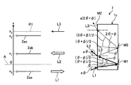
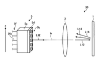
- FIG. 1 is a schematic configuration diagram of an optical switch according to the first embodiment.
- the optical switch 10 includes a spatial light modulator 1, an optical input / output device 2, and a condenser lens 3.
- the light input to or output from the optical switch 10 is not particularly limited, but is signal light for optical communication having a wavelength of 1520 to 1620 nm, for example.
- the light input / output device 2 includes a light input / output port 2a that receives light from the outside or outputs light to the outside, and a plurality of collimator lenses 2b.
- the optical input / output port 2a is obtained by arranging optical fiber ports 2aa to 2ae in an array in a predetermined arrangement direction (x-axis direction in the figure).
- the collimator lens 2b is provided corresponding to each of the optical fiber ports 2aa to 2ae.
- the collimator lens 2b has a function of collimating the light output from the optical fiber port or condensing and coupling the input parallel light to the optical fiber port.
- the light emitted from the optical fiber can be approximated as a Gaussian beam.
- the beam diameter gradually decreases as it propagates, becomes minimum at the beam waist position, and increases again.
- the condensing lens 3 is disposed between the light input / output device 2 and the spatial light modulator 1, and is optically coupled to the light input / output port 2a and the spatial light modulator 1.
- Reference symbol A indicates the optical axis of the condenser lens 3.
- the condensing lens 3 may be comprised with the lens of 1 sheet, and may be comprised with the lens of several sheets. Further, when the focal length of the condenser lens 3 is f, the spatial light modulator 1 is arranged at a distance f from the condenser lens 3. That is, the spatial light modulator 1 is disposed at the focal position of the condenser lens 3.
- the condensing lens 3 is arranged at a distance d + f away from the collimator lens 2b to reduce the coupling loss when recombining with the optical fiber 2a. Can do.
- the optical fiber port 2aa located closest to the optical axis A among the optical input / output ports 2a is set as a common optical fiber port (Com port) through which light is input from the outside.
- the other four optical fiber ports 2ab to 2ae are set as optical fiber ports for outputting light to the outside. That is, the optical switch 10 functions as a 1 ⁇ 4 optical switch. It is assumed that the optical fiber port 2aa is not on the optical axis A.
- FIG. 2 is an exploded view of the spatial light modulator 1 shown in FIG.
- the spatial light modulator 1 is an LCOS, and a pixel electrode group 1b, which is a reflective layer having a reflectance of approximately 100%, is formed on a silicon substrate 1a on which a liquid crystal driving circuit is formed.
- the liquid crystal layer 1c which is a light modulation layer
- an alignment film 1d, an ITO (Indium Tin Oxide) electrode 1e, and a cover glass 1f are sequentially laminated.
- An alignment film may be provided between the pixel electrode group 1b and the liquid crystal layer 1c as necessary.
- the alignment film 1d, the ITO electrode 1e, and the cover glass 1f are referred to as a light incident layer 1g.
- the spatial light modulator 1 can be controlled so that the liquid crystal layer 1c has a refractive index gradation in a predetermined direction by applying a voltage between the pixel electrode group 1b and the ITO electrode 1e. Then, by adjusting the gradation of the refractive index, when the light incident from the light incident layer 1g side is reflected by the pixel electrode group 1b and propagates through the liquid crystal layer 1c, the light is diffracted at a predetermined diffraction angle. Can be adjusted as follows.
- the spatial light modulator 1 is arranged so that the arrangement direction of the optical fiber ports 2aa to 2ae of the light input / output port 2a coincides with the direction of gradation of the refractive index of the liquid crystal layer 1c.
- the spatial light modulator 1 can output the light incident from the optical fiber port 2aa to any one of the other optical fiber ports 2ab to 2ae by controlling the voltage applied to the liquid crystal layer 1c.
- the light emission angle can be controlled.
- FIG. 3 is a diagram showing a specific configuration of the optical input / output device 2 shown in FIG.
- the optical input / output device 2 includes an optical input / output port 2a, a plurality of collimator lenses 2b, an optical fiber fixing substrate 2c for inserting and fixing each optical fiber port of the optical input / output port 2a, A transparent spacer 2d for holding the collimator lens 2b is attached to the optical fiber fixing substrate 2c.
- Each optical fiber port is fixed so that its light exit end face is flush with the surface of the optical fiber fixing base 2c to which the spacer portion 2d is attached.
- the thickness of the spacer portion 2d is substantially equivalent to the focal length of the collimator lens 2b.
- optical switch 10 As an operation example 1-1 of the optical switch 10, a case where the path of light input from the optical fiber port 2aa is switched to the optical fiber port 2ab as shown in FIG. 1 will be described.
- the optical fiber port 2aa receives light from the outside, and the corresponding collimator lens 2b converts the input light into parallel light.
- the condensing lens 3 condenses the parallel light L1 on the spatial light modulator 1.
- the spatial light modulator 1 controls the voltage applied to the liquid crystal layer 1c to spatially modulate and diffract the incident and incident light L1, and outputs the diffracted light L2 toward the optical fiber port 2ab. To do.
- the condenser lens 3 makes the diffracted light L2 parallel to the optical axis A.
- the collimator lens 2b corresponding to the optical fiber port 2ab collects the light L2 parallel to the optical axis A and couples it to the optical fiber port 2ab.
- the optical fiber port 2ab outputs the combined light to the outside.
- the optical switch 10 switches the path of light input from the optical fiber port 2aa to the optical fiber port 2ab. Similarly, the optical switch 10 switches the path of light input from the optical fiber port 2aa, which is a Com port, to one of the other optical fiber ports 2ab to 2ae under the control of the spatial light modulator 1. be able to.
- the optical switch 10 when the light L2 diffracted by the spatial light modulator 1 is output toward the optical fiber port 2ab, multiple reflection occurs due to internal reflection of the spatial light modulator 1, and the diffracted light L2 A part is emitted as secondary reflected light.
- the optical fiber ports 2aa, 2ab, 2ac when the position of the optical axis A of the condenser lens 3 is the coordinate origin of the x axis and the upward direction on the paper is a positive direction. Is set to x 0 , x 1 , and x 2 , the following equation (1) is established.
- the optical switch 10 Since the optical fiber ports 2aa, 2ab, and 2ac are arranged so that the formula (1) is satisfied, the secondary reflected light does not reach the optical fiber port 2ac, so that it can be output to the optical fiber port 2ac unintentionally. Is prevented. As a result, the optical switch 10 has good crosstalk characteristics.
- FIG. 4 is a diagram for explaining the behavior of light in the spatial light modulator 1 of the optical switch 10 shown in FIG.
- the condenser lens 3 is not shown.
- the clockwise direction is the positive direction of the angle.
- a one-dot chain line in the figure indicates a normal line of the surface of the liquid crystal layer 1c.
- n 1 sin ⁇ 1 n 2 sin ⁇ 2 (2)
- n 1 represents the refractive index of the incident side medium
- ⁇ 1 represents the incident angle of the light L1 with respect to the liquid crystal layer 1c
- n 2 represents the refractive index of the liquid crystal layer 1c
- ⁇ 2 represents the refractive angle of the light L1.
- the outgoing angle of the diffracted light L2 with respect to the liquid crystal layer 1c is a ⁇ .
- the diffraction angle ⁇ is set so that the light L2 is input to the optical fiber port 2ab after being converted into light that travels parallel to the optical axis A by the condenser lens 3. Therefore, the coordinates x 1 of optical fiber ports 2ab can be approximately expressed by the following equation (4).
- the reflection surface M2 conceptually indicates an internal reflection surface present in the light incident layer 1g. Actually, Snell's law must be applied every time a plurality of surfaces are refracted, but it is omitted here for the sake of clarity.
- Snell's law must be applied every time a plurality of surfaces are refracted, but it is omitted here for the sake of clarity.
- the normal line of the reflection surface (indicated by a broken line in the drawing) forms an angle ( ⁇ + ⁇ ) / 2 with respect to the normal line of the surface of the liquid crystal layer 1c.
- the secondary reflected light L3 is diffracted at a diffraction angle (2 ⁇ + ⁇ ) with respect to the normal line of the surface of the liquid crystal layer 1c.
- the secondary reflected light L3 is emitted from the spatial light modulator 1 at an emission angle a (2 ⁇ + ⁇ ).
- the secondary reflected light L3 generated by the multiple reflection inside the spatial light modulator 1 reaches the position of the x coordinate represented by the equation (5).
- the coordinate x 2 of the optical fiber port 2ac is arranged so that x 2 ⁇ 2x 1 + x 0 that is Expression (1) is established. ing. Accordingly, the secondary reflected light L3 does not reach the optical fiber port 2ac but is prevented from being output therefrom. As a result, the optical switch 10 has good crosstalk characteristics.
- the coordinate x 0 of the optical fiber port 2aa is a negative value.
- the optical fiber port 2aa is arranged so that the coordinate x 0 is a positive value, the above formula ( 1) to (5) hold true. Therefore, if the coordinate x 0 is also a positive value, the optical switch 10 is crosstalk characteristic is improved.
- the optical fiber port 2aa is not arranged on the optical axis A of the condenser lens 3, x 0 ⁇ 0.
- the diffraction direction by the liquid crystal layer 1c is in the negative direction of the x-axis, but the light emitted from the spatial light modulator 1 is 2 by the same principle as in the operation example 1-1. Since the next reflected light is prevented from being unintentionally output to another optical fiber port 2ae, the optical switch 10 has good crosstalk characteristics.
- the optical switch 10 according to Embodiment 1 prevents the secondary reflected light emitted from the spatial light modulator 1 from being output to an unintended optical fiber port. It will be good.
- the optical fiber ports 2aa to 2ae may be arranged at equal intervals or at unequal intervals.
- a Com port for inputting light among light input / output ports is arranged on the optical axis of the condenser lens.
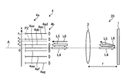
- FIG. 5 is a schematic configuration diagram of the optical switch according to the second embodiment.
- the optical switch 20 includes a spatial light modulator 1, an optical input / output device 4, and a condenser lens 3.
- the light input / output device 4 includes a light input / output port 4a and a plurality of collimator lenses 4b.
- the optical input / output port 4a is obtained by arranging optical fiber ports 4aa to 4ag in an array in a predetermined arrangement direction (x-axis direction in the figure).
- the collimator lens 4b is provided corresponding to each of the optical fiber ports 4aa to 4ag.
- the collimator lens 4b has a function of collimating the light output from the optical fiber port or condensing and coupling the input parallel light to the optical fiber port.
- the specific configuration of the optical input / output device 4 is the same as that shown in FIG.
- the spatial light modulator 1 and the condenser lens 3 are the same as those in the first embodiment. As in the first embodiment, the spatial light modulator 1 is disposed at the focal point of the condenser lens 3. The spatial light modulator 1 is arranged so that the arrangement direction of the optical fiber ports 4aa to 4ag of the light input / output port 2a coincides with the gradation direction of the refractive index of the liquid crystal layer 1c.
- the optical switch 20 among the optical input / output ports 4a, the optical fiber port 4aa disposed on the optical axis A is set as a Com port to which light is input from the outside, and the other six optical fiber ports. 4ab to 4ag are set as optical fiber ports for outputting light to the outside. That is, the optical switch 20 functions as a 1 ⁇ 6 optical switch.
- the optical fiber port 4aa receives light from the outside, and the corresponding collimator lens 4b makes the input light parallel light.
- the condensing lens 3 condenses the collimated light L4 on the spatial light modulator 1.
- the spatial light modulator 1 controls the voltage applied to the liquid crystal layer 1c to spatially modulate and diffract the incident and incident light L4 and direct the diffracted light L5 toward the optical fiber port 4ab. Output.
- the condenser lens 3 makes the diffracted light L5 parallel to the optical axis A.
- the collimator lens 4b corresponding to the optical fiber port 4ab collects the light L5 parallel to the optical axis A and couples it to the optical fiber port 4ab.
- the optical fiber port 4ab outputs the combined light to the outside.
- the optical switch 20 switches the path of light input from the optical fiber port 4aa to the optical fiber port 4ab.
- the optical switch 20 can switch the path of light input from the optical fiber port 4aa, which is a Com port, to any of the other optical fiber ports 4ab to 4ag.
- optical fiber ports 4ab and 4ac are arranged so that the following expression (7) is established.
- the optical switch 20 has good crosstalk characteristics. It becomes.
- FIG. 6 is a diagram for explaining the behavior of light in the spatial light modulator 1 of the optical switch 20 shown in FIG. In FIG. 6, the condenser lens 3 is not shown.
- FIG. 6 differs from FIG. 4 in that the light L4 input from the optical fiber port 4aa is incident on the liquid crystal layer 1c of the spatial light modulator 1 with an incident angle of zero. Since the optical fiber port 4aa is disposed on the optical axis A of the condensing lens 3, the traveling direction of the light L4 is not refracted even when passing through the condensing lens 3, and thus the incident angle becomes zero. .
- the pixel electrode M1 reflects the light L4, and the liquid crystal layer 1c diffracts at a diffraction angle ⁇ with respect to the normal of the surface of the liquid crystal layer 1c by the effect of refractive index gradation.
- the outgoing angle of the diffracted light L5 with respect to the liquid crystal layer 1c is a ⁇ .
- the diffraction angle ⁇ is set so that the light L4 is input to the optical fiber port 4ab after being converted into light that travels parallel to the optical axis A by the condenser lens 3. Therefore, the coordinates x 4 fiber optic port 4ab can be approximately expressed by the following equation (8).
- the diffracted light L4 is emitted from the spatial light modulator 1 by the reflecting surface M2, a part of the light is reflected and is reflected as a secondary reflected light L6 to the pixel electrode M3 adjacent to the pixel electrode M1.
- the pixel electrode M3 reflects the secondary reflected light L6, and the liquid crystal layer 1c diffracts at a diffraction angle (2 ⁇ ) with respect to the normal line of the surface of the liquid crystal layer 1c due to the effect of the refractive index gradation. Thereafter, the secondary reflected light L6 is emitted from the spatial light modulator 1 at an emission angle (2a ⁇ ).
- Equation (6) is derived.
- the optical switch 20 according to the second embodiment, the coordinates x 5 optical fiber ports 4ac, are arranged so as equation (7) holds. Therefore, the secondary reflected light L6 does not reach the optical fiber port 4ac but is prevented from being output therefrom. As a result, the optical switch 20 has good crosstalk characteristics.
- the optical switch 20 prevents the secondary reflected light L6 emitted from the spatial light modulator 1 from being output to an unintended optical fiber port. Will be good.
- the above equation (6) may be satisfied, so that it is necessary to set the optical fiber ports 4aa to 4ae at unequal intervals.
- X 7 9.6 mm
- x 4 ′ ⁇ 2.4 mm
- x 5 ′ ⁇ 4.8 mm
- x 7 ′ ⁇ 9.6 mm
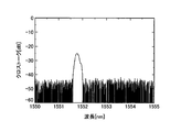
- FIG. 7 is a diagram showing the measurement result of the crosstalk of the optical switch of the conventional example.
- the light output from the optical fiber ports of the coordinate x 4 as a reference (0 dB) shows the light output from the optical fiber ports of the coordinate x 5.
- 25 dB lower reflected light will have been output from the optical fiber ports of the coordinate x 5 with respect to the reference.
- the specifications required in optical communication are strict, so even a very small crosstalk of 25 dB, which does not cause a problem in display applications, becomes a problem.
- the optical switch 20 functions as a 1 ⁇ 6 optical switch. Below, the case where the optical switch 20 is made to function as a 6x1 optical switch as this modification is demonstrated.
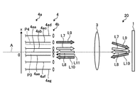
- FIG. 8 is a schematic configuration diagram of an optical switch according to a modification of the second embodiment.
- the schematic configuration of the optical switch 20 shown in FIG. 8 is the same as that shown in FIG. 5, but in this modification, the six optical fiber ports 4ab to 4ag out of the optical input / output port 4a receive light from the outside.
- the optical fiber port 4aa disposed on the optical axis A is set as a Com port that outputs light to the outside. That is, the optical switch 20 functions as a 6 ⁇ 1 optical switch.
- the optical switch 20 switches the path of light input from the optical fiber port 4ba to the optical fiber port 4aa.
- the optical switch 20 can switch the path of light input from any of the optical fiber ports 4ab to 4ag to the optical fiber port 4aa which is a Com port.
- the light L9 is input from, for example, another optical fiber port 4ac in a state where the optical switch 20 is operating as in the operation example 2 as a 6 ⁇ 1 optical switch. Even if the light L9 normally reaches the spatial light modulator 1 via the condenser lens 3 and is diffracted, the diffracted light L10 reaches the optical fiber port 4aa and is output. There is no. The reason is that, in the second operation example, the diffraction angle of the spatial light modulator 1 is set so as to output the light input from the optical fiber port 4ab to the optical fiber port 4aa.
- the optical switch 20 according to this modification is used as a 6 ⁇ 1 optical switch, the crosstalk characteristics are good.
- FIG. 9 is a diagram for explaining the behavior of light in the spatial light modulator 1 when the optical fiber ports 4aa, 4ab, and 4ac are arranged at equal intervals.
- the light L7 input from the optical fiber port 4ab passes through a path opposite to the light L4 and L5 in FIG. 6, and is emitted as the diffracted light L8, and then the light. It reaches the fiber port 4aa and is output.
- the optical fiber port 4ac is disposed at the position P4 shown in FIG. 8, the light L9 ′ input from the optical fiber port 4ac passes through a path opposite to the secondary reflected light L6 in FIG. And is emitted as diffracted light L10 '.
- the secondary reflected light L11 ′ of the light L10 ′ is generated by the reflecting surface M2, and this secondary reflected light L11 ′ is diffracted through a path opposite to the light L4 in FIG. The light is emitted in the same direction as the light L8. Therefore, the secondary reflected light L11 ′ causes the port-to-port crosstalk characteristics to deteriorate.
- the light input / output port is formed of an optical fiber, but it may be formed of an optical waveguide made of a glass material or a semiconductor material.
- an optical switch in which an optical input / output port is composed of a quartz glass planar light wave circuit (PLC) will be described.
- FIG. 10 is a schematic configuration diagram of an optical switch according to the third embodiment.
- the optical switch 30 has a configuration in which the optical input / output device 4 is replaced with the optical input / output device 5 in the configuration of the optical switch 20 shown in FIG.
- the optical input / output device 5 includes an optical input / output port 5a made of silica-based PLC, a plurality of collimator lenses 5b, a spacer portion 5d that is attached to the optical input / output port 5a and holds the collimator lens 5b, An optical fiber array 5f for connecting the input / output port 5a and an external path is provided.
- an optical waveguide is formed as an input or output port so as to optically connect the optical fiber array 5f and the corresponding collimator lens 5b. Similar to the optical fiber ports 2aa to 2ac and 2ae to 2af of the first embodiment, these optical waveguide ports are arranged in an array in the x-axis direction in the figure, and the x coordinate is also the optical fiber ports 2aa to 2af. It is set similarly to 2ac, 2ae to 2af.
- this optical switch 30 An example of the operation of this optical switch 30 will be described.
- the light L12 is input from the optical fiber 5fa constituting the optical fiber array 5f to the optical waveguide port disposed on the optical axis A of the condenser lens 3 which is the Com port of the light input / output port 5a.
- the condensing lens 3 condenses the light L13 on the spatial light modulator 1, and the spatial light modulator 1 diffracts the light L13 and outputs the light L13 toward a predetermined optical waveguide port.
- the secondary reflected light L14 is generated, but the secondary reflected light L14 does not reach other optical waveguide ports as in the second embodiment. Therefore, this optical switch 30 has a good crosstalk.
- the optical switch according to the fourth embodiment has an arrayed wave guide grating (AWG) as a wavelength multiplexer / demultiplexer, and functions as a wavelength selective optical switch.
- AMG arrayed wave guide grating
- FIG. 11 is a schematic configuration diagram of an optical switch according to the fourth embodiment.
- the optical switch 40 has a configuration in which the optical input / output device 2 is replaced with the optical input / output device 6 in the configuration of the optical switch 10 shown in FIG. 2.
- the spatial light modulator six spatial light modulators 1 may be used, or one spatial light modulator 1 may be divided into six regions and each region may be controlled independently. May be used for
- the optical input / output device 6 is attached to the optical input / output port 6a formed by laminating AWGs 6aa to 6ae made of quartz glass, a plurality of collimator lenses 6b, the optical input / output port 6a, and holds the collimator lens 6b.
- the spacer 6d is provided with an optical fiber array 6f for connecting the optical input / output port 6a and an external path.
- the AWGs 6aa to 6ae have a function of outputting light of wavelengths ⁇ 1 , ⁇ 2 , ⁇ 3 , ⁇ 4 , ⁇ 5 , and ⁇ 6 input from the input port from the output port corresponding to each wavelength.
- the fiber array 6f is connected to each input port of the AWGs 6aa to 6ae.
- the collimator lens 6b is provided corresponding to each output port of the AWGs 6aa to 6ae.
- the output ports of the AWGs 6aa to 6ae the output ports of the same wavelength are arranged in an array in the x-axis direction in the figure, and the x coordinates thereof are the optical fiber ports 2aa to 2ac of the optical switch 10 in FIG.
- the output ports of the wavelengths ⁇ 1 of the AWGs 6aa to 6ae arranged in an array in the x-axis direction are surrounded by a broken line.
- Other optical switches (not shown) are arranged side by side with the illustrated spatial light modulator 1 so as to correspond to the output ports of the respective wavelengths.
- light L15 including light of wavelengths ⁇ 1, ⁇ 2, ⁇ 3, ⁇ 4, ⁇ 5, and ⁇ 6 is input from the optical fiber 6fa connected to the AWG 6aa of the optical input / output port 6a.
- the AWG 6aa outputs the light L16 having the wavelength ⁇ 2 from the output port OP1 corresponding to the wavelength ⁇ 2.
- the condensing lens 3 condenses the light L16 on the spatial light modulator 1 corresponding to the wavelength ⁇ 2, and the spatial light modulator 1 diffracts the light L16 to obtain a predetermined AWG among the AWGs 6ab to 6ae as the light L17.
- this optical switch 40 has a good crosstalk. Note that the optical switch 40 functions as a wavelength selective optical switch having good crosstalk by switching light of other wavelengths to a predetermined path by a spatial light modulator corresponding to the wavelength.
- AWG is used as the wavelength multiplexer / demultiplexer.
- the wavelength multiplexer / demultiplexer may be configured by appropriately combining wavelength selective elements such as a fiber melting type and a filter type.
- the optical switch according to the fifth embodiment is a wavelength selective optical switch that selects an optical signal having a predetermined wavelength from an input wavelength-multiplexed optical signal and switches the path for each wavelength of the optical signal and outputs it.
- FIG. 12 is a block diagram showing a configuration of the optical switch according to the fifth embodiment.
- the optical switch 100 includes an optical input / output device 2 connected to an external path, an anamorphic prism pair 61 and a diffraction grating 62 that are sequentially arranged with respect to the optical input / output device 2.
- a monitor element 68 for controlling ⁇ 1D and a control circuit 69 are provided.
- the optical input / output device 2 and the condenser lens 3 are the same as those in the first embodiment.
- Each optical fiber port of the optical input / output device 2 is arranged at the same x coordinate as in the first embodiment when the position of the condenser lens 3 is the origin of the x axis.
- the spatial light modulators 1A to 1D are all the same as the spatial light modulator 1 of the first embodiment.
- the condenser lens 3 and the spatial light modulators 1A to 1D are separated from each other by the focal length f of the condenser lens 3.
- each element is arranged at an angle.
- the elements are arranged in series for simplification. ing.
- FIG. 13 is an explanatory diagram for explaining the operation of the optical switch 100 shown in FIG.
- FIG. 13 is a diagram of the optical switch 100 viewed from a direction perpendicular to the x-axis direction in FIG.
- the optical input / output device 2 outputs the wavelength multiplexed optical signal OS1 input from a certain path to the optical fiber port 2aa which is a Com port to the anamorphic prism pair 61 as parallel light.
- the anamorphic prism pair 61 expands the beam diameter of the wavelength multiplexed optical signal OS1 in the grating arrangement direction of the diffraction grating 62 so as to increase the wavelength selection resolution so that the wavelength multiplexed optical signal OS1 hits many gratings. I have to.
- the diffraction grating 62 outputs an optical signal OS1a having a predetermined wavelength included in the incident wavelength multiplexed optical signal OS1 at a predetermined angle.
- the condenser lens 3 condenses the optical signal OS1a on the spatial light modulator 1A through the ⁇ / 4 wavelength plate 63.
- the spatial light modulator 1A diffracts the collected optical signal OS1a, and sequentially passes through the ⁇ / 4 wavelength plate 63, the condenser lens 3, the diffraction grating 62, and the anamorphic prism pair 61 as an optical signal OS2.
- the ⁇ / 4 wavelength plate 63 changes the polarization state of the optical signal OS1a and the optical signal OS2 so that the polarization states of the light are orthogonal to each other. Thereby, the polarization dependence of the anamorphic prism pair 61 and the diffraction grating 62 is compensated.
- the diffraction grating 62 outputs the optical signals OS1b, OS1c, OS1d having other predetermined wavelengths included in the wavelength multiplexed optical signal OS1 to other predetermined angles, respectively.
- Each of the optical signals OS1b, OS1c, OS1d is diffracted by the spatial light modulators 1B, 1C, 1D, respectively, and as the optical signals OS3, OS4, OS5, a ⁇ / 4 wavelength plate 63, a condenser lens 3, a diffraction grating 62, an analog
- the signals are output to the corresponding optical fiber ports 2ac, 2ad, and 2ae via the morphic prism pair 61 sequentially.
- the spatial light modulators 1A to 1D monitor the wavelength and intensity of the light that the monitor element 68 branches a part of the optical signals OS2 to OS5, and based on the results of the monitoring, the spatial light modulators 1A to 1D are independent. By controlling so that the diffraction angles of the respective optical signals OS2 to OS5 are optimized.
- the optical signals OS2 to OS5 can be branched by, for example, providing a branching coupler in a part of the optical input / output device 2 or providing a branching mirror at an appropriate position in the optical switch 100.
- the monitor element 68 is composed of, for example, an AWG and a plurality of photodiodes.
- the spatial light modulator 1A diffracts the optical signal OS1a
- secondary reflected light generated inside the spatial light modulator 1A is emitted.
- the secondary reflected light reaches the optical input / output device 2 via the ⁇ / 4 wavelength plate 63, the condenser lens 3, the diffraction grating 62, and the anamorphic prism pair 61 in order.
- the secondary reflected light does not reach any of the other optical fiber ports 2ac to 2ae by the same operation as in the first embodiment.
- the other optical signals OS1b, OS1c, and OS1d also cause secondary reflection inside the spatial light modulators 1B to 1D due to the above, and even when they are emitted, they reach other than predetermined optical fiber ports. There is nothing. Therefore, this optical switch 100 has good crosstalk between ports.
- the optical switch is 1 ⁇ 4, 1 ⁇ 6, 6 ⁇ 1, etc.
- the number of ports through which light is input and output is not particularly limited, and is an N ⁇ M optical switch. I just need it. However, since one of N and M needs to be 2 or more, 3 or more ports are required. In the configuration using the wavelength multiplexer / demultiplexer as in the fourth embodiment, three or more wavelength multiplexers / demultiplexers are required.
- the secondary reflected light generated by the internal reflection of the spatial light modulator is prevented from being output to an unintended port.
- Higher-order reflected light is considerably weaker than secondary reflected light, but it is more preferable not to be output to an unintended port.
- the coordinates of the first port to which light is input, the second port and the third port that output light input from the first port are x 0 , x 1 , and x 2 , respectively.
- x 2 ⁇ 2kx 1 + x 0 may be satisfied.
- the Com port through which light is always input or output among the light input / output ports is arranged on or near the optical axis of the condenser lens. Yes.
- the Com port is arranged on the optical axis of the condensing lens, it is easy to perform alignment when assembling the optical switch, and the spatial light modulator can have zero incident or outgoing angle of light. This is particularly preferable because it becomes easier to control.
- the present invention is not limited to this, and the port farthest from the optical axis among the optical input / output ports may be a Com port.
- the spatial light modulation layer is a liquid crystal, but it is not particularly limited as long as it is a member capable of spatially modulating light.
- the spatial light modulator is of a reflective type, but may be of a transmissive type.
- the reflective layer does not have a reflectance of almost 100% but has a certain degree of translucency. Even with such a transmissive spatial light modulator, internal multiple reflection can occur between layers sandwiching the spatial light modulation layer, and therefore the present invention can be applied.
- the present invention is not limited by the above embodiment. What comprised each component of each said embodiment combining suitably is also contained in this invention.
- the optical input / output device of the second embodiment may be applied to the optical switch according to the fifth embodiment.
- the optical switch according to the present invention is suitable mainly for use in optical communication.
Abstract
An optical switch is provided with: optical input/output ports in which three or more ports are arranged in a prescribed array direction; a spatial light modulator that comprises an incident light layer and a light reflection layer, and a spatial light modulation layer disposed between the incident light layer and the light reflection layer, and that spatially modulates light that strikes the incident light layer from one of the optical input/output ports, and outputs the light toward one of the other optical input/output ports; and a condenser lens that optically joins the optical input/output ports and the spatial light modulator. If coordinate axes are taken in the array direction of the optical input/output ports, and the position of the optical axis of the condenser lens is regarded as the origin of the coordinate axes, when the coordinates of a first port to which light in the optical input/output ports is inputted or which outputs the light, and a second port and third port which output or receive the light that is input or output by the first port are regarded as x0, x1 and x2 (where x1 and x2 > 0), respectively, x2 ≠ 2x1 + x0 holds true.
Description
本発明は、光スイッチに関するものである。
The present invention relates to an optical switch.
光伝送システムにおいて、波長多重光信号等の光信号の経路を切り替えるために、光スイッチが使用されている。このような光スイッチには、光信号の経路を切り替えるために、LCOS(Liquid Crystal On Silicon)を用いたものがある(特許文献1、2参照)。LCOSは、入射された光の位相を液晶によって変調し、回折させることができる空間光変調器である。したがって、LCOSを用いた光スイッチでは、或る経路から入射された光信号を、LCOSによって回折させて、特定の経路に出力することにより、光スイッチ動作を実現している。
In an optical transmission system, an optical switch is used to switch a path of an optical signal such as a wavelength multiplexed optical signal. Some of such optical switches use LCOS (Liquid Crystal On Silicon) in order to switch the path of an optical signal (see Patent Documents 1 and 2). The LCOS is a spatial light modulator capable of modulating and diffracting the phase of incident light with a liquid crystal. Therefore, in an optical switch using LCOS, an optical switch operation is realized by diffracting an optical signal incident from a certain path by LCOS and outputting it to a specific path.
特許文献1、2に開示される光スイッチでは、光信号が入力される入力ポートと、光信号を出力する出力ポートとが、所定の方向に沿って等間隔で配列している。また、入力ポートはレンズの光軸上に配置されている。したがって、LCOSは、入射光の角度をこの配列方向に回折させるように構成されている。また、入力および出力ポートの数がそれぞれN、M(N、Mは1以上の整数)の光スイッチは、N×M光スイッチと呼ばれる。
In the optical switches disclosed in Patent Documents 1 and 2, an input port to which an optical signal is input and an output port from which the optical signal is output are arranged at equal intervals along a predetermined direction. The input port is arranged on the optical axis of the lens. Therefore, the LCOS is configured to diffract the angle of incident light in this arrangement direction. An optical switch having N and M (N and M are integers of 1 or more) input and output ports, respectively, is called an N × M optical switch.
しかしながら、本発明者らが特許文献1、2に開示される構成の光スイッチの特性について精査したところ、所定の入力ポートから入力した光信号を所定の出力ポートに出力させるような光スイッチ動作をさせる場合に、意図しない他の出力ポートにも光信号の一部が出力されてしまう場合があるという問題を見出した。このように光スイッチに入力させた光信号の一部が意図しない出力ポートにも出力してしまうと、出力ポート間のクロストーク特性が劣化するという問題が生じる。
However, the present inventors have scrutinized the characteristics of the optical switch having the configuration disclosed in Patent Documents 1 and 2, and found that an optical switch operation that outputs an optical signal input from a predetermined input port to a predetermined output port is performed. In this case, it has been found that a part of the optical signal may be output to other unintended output ports. Thus, if a part of the optical signal input to the optical switch is also output to an unintended output port, there arises a problem that the crosstalk characteristic between the output ports deteriorates.
本発明は、上記に鑑みてなされたものであって、良好なクロストーク特性を有する光スイッチを提供することを目的とする。
The present invention has been made in view of the above, and an object thereof is to provide an optical switch having good crosstalk characteristics.
上述した課題を解決し、目的を達成するために、本発明に係る光スイッチは、外部から光が入力される、または外部に光を出力する3以上のポートが所定の配列方向に沿って配列した光入出力ポートと、光入射層と、光反射層と、前記光入射層と前記光反射層との間に設けられた空間光変調層とを有し、前記光入出力ポートのいずれかのポートから前記光入射層に入射した光を空間変調して前記光入出力ポートの他のいずれかのポートに向けて出力する空間光変調器と、前記光入出力ポートと前記空間光変調器との間に配置され、前記光入出力ポートと前記空間光変調器と光学的に結合させる集光レンズと、を備え、前記光入出力ポートの配列方向に沿った座標軸をとり、前記集光レンズの光軸の位置を該座標軸の原点とした場合に、前記光入出力ポートにおいて光が入力されるまたは出力する第1ポート、前記第1ポートから入力または出力する光を出力または入力される第2ポートおよび第3ポートの座標をそれぞれx0、x1、およびx2(ただし、x1、x2>0)とすると、x2≠2x1+x0が成り立つことを特徴とする。
In order to solve the above-described problems and achieve the object, the optical switch according to the present invention includes three or more ports that receive light from the outside or output light to the outside along a predetermined arrangement direction. A light input / output port, a light incident layer, a light reflection layer, and a spatial light modulation layer provided between the light incident layer and the light reflection layer, A spatial light modulator that spatially modulates light incident on the light incident layer from the port and outputs the modulated light to any other port of the light input / output port, the light input / output port, and the spatial light modulator A condensing lens that is optically coupled to the light input / output port and the spatial light modulator, takes a coordinate axis along the arrangement direction of the light input / output port, and collects the light When the position of the optical axis of the lens is the origin of the coordinate axis, First port is being or output light is input at an output port, said first and second and third ports of the coordinate is output or input an input or output light from the port, respectively x 0, x 1, and x 2 (where x 1 , x 2 > 0), x 2 ≠ 2x 1 + x 0 holds.
また、本発明に係る光スイッチは、上記の発明において、前記第1ポートの座標x0がゼロ以外の値であり、前記光入出力ポートにおいて隣接するポート間の間隔が等間隔または不等間隔であることを特徴とする。
Further, the optical switch according to the present invention, in the above invention, the coordinate x 0 of the first port is a non-zero value, the interval is equal intervals or unequal intervals between adjacent ports in said optical input and output ports It is characterized by being.
また、本発明に係る光スイッチは、上記の発明において、前記第1ポートの座標x0がゼロであり、前記光入出力ポートにおいて隣接するポート間の間隔が不等間隔であることを特徴とする。
Further, the optical switch according to the present invention, in the above invention, the coordinates x 0 is zero of the first port, and wherein the spacing between adjacent ports in said optical input and output ports are unequal To do.
また、本発明に係る光スイッチは、上記の発明において、前記第1ポートは、前記光入出力ポートの他のポートに出力する光が入力されるポートであることを特徴とする。
In the optical switch according to the present invention as set forth in the invention described above, the first port is a port to which light output to another port of the optical input / output port is input.
また、本発明に係る光スイッチは、上記の発明において、前記第1ポートは、前記光入出力ポートの他のポートから入力される光が出力するポートであることを特徴とする。
In the optical switch according to the present invention as set forth in the invention described above, the first port is a port from which light input from another port of the optical input / output port is output.
また、本発明に係る光スイッチは、上記の発明において、前記空間光変調器はLCOSであることを特徴とする。
The optical switch according to the present invention is characterized in that, in the above invention, the spatial light modulator is an LCOS.
また、本発明に係る光スイッチは、上記の発明において、前記光入出力ポートと前記空間光変調器との間に設けられた光分散素子を備え、波長選択光スイッチとして機能することを特徴とする。
An optical switch according to the present invention is characterized in that, in the above invention, the optical switch includes an optical dispersion element provided between the optical input / output port and the spatial light modulator, and functions as a wavelength selective optical switch. To do.
また、本発明に係る光スイッチは、上記の発明において、前記光入出力ポートは、3以上の波長合分波器を有し、前記各波長合分波器において同一波長を出力する各ポートが、前記配列方向に配列したポートを構成し、波長選択光スイッチとして機能することを特徴とする。
In the optical switch according to the present invention, the optical input / output port includes three or more wavelength multiplexers / demultiplexers, and each port outputting the same wavelength in each wavelength multiplexer / demultiplexer includes: The ports arranged in the arrangement direction are configured to function as a wavelength selective optical switch.
また、本発明に係る光スイッチは、上記の発明において、前記波長多重合分波器がアレイ型光導波路グレーティングであることを特徴とする。
Also, the optical switch according to the present invention is characterized in that, in the above-mentioned invention, the wavelength multi-polymerization demultiplexer is an array type optical waveguide grating.
本発明によれば、空間光変調器内での多重反射により発生した反射光が意図しない出力ポートに結合することが防止されるので、良好なクロストーク特性を有する光スイッチを実現できるという効果を奏する。
According to the present invention, since the reflected light generated by the multiple reflection in the spatial light modulator is prevented from being coupled to an unintended output port, an optical switch having a good crosstalk characteristic can be realized. Play.
以下に、図面を参照して本発明に係る光スイッチの実施の形態を詳細に説明する。なお、この実施の形態によりこの発明が限定されるものではない。また、各図面において、同一または対応する要素には適宜同一の符号を付している。さらに、図面は模式的なものであり、各層の厚みと幅との関係、各層の比率などは、現実のものとは異なる場合があることに留意する必要がある。図面の相互間においても、互いの寸法の関係や比率が異なる部分が含まれている場合がある。
Embodiments of an optical switch according to the present invention will be described in detail below with reference to the drawings. Note that the present invention is not limited to the embodiments. Moreover, in each drawing, the same code | symbol is attached | subjected suitably to the same or corresponding element. Furthermore, it should be noted that the drawings are schematic, and the relationship between the thickness and width of each layer, the ratio of each layer, and the like may differ from the actual ones. Even between the drawings, there are cases in which portions having different dimensional relationships and ratios are included.
(実施の形態1)
図1は、実施の形態1に係る光スイッチの概略構成図である。図1に示すように、この光スイッチ10は、空間光変調器1と、光入出力器2と、集光レンズ3とを備えている。なお、本光スイッチ10に入力または出力される光は特に限定されないが、たとえば波長1520~1620nmの光通信用の信号光である。 (Embodiment 1)
FIG. 1 is a schematic configuration diagram of an optical switch according to the first embodiment. As shown in FIG. 1, theoptical switch 10 includes a spatial light modulator 1, an optical input / output device 2, and a condenser lens 3. The light input to or output from the optical switch 10 is not particularly limited, but is signal light for optical communication having a wavelength of 1520 to 1620 nm, for example.
図1は、実施の形態1に係る光スイッチの概略構成図である。図1に示すように、この光スイッチ10は、空間光変調器1と、光入出力器2と、集光レンズ3とを備えている。なお、本光スイッチ10に入力または出力される光は特に限定されないが、たとえば波長1520~1620nmの光通信用の信号光である。 (Embodiment 1)
FIG. 1 is a schematic configuration diagram of an optical switch according to the first embodiment. As shown in FIG. 1, the
光入出力器2は、外部から光が入力される、または外部に光を出力する光入出力ポート2aと、複数のコリメータレンズ2bとを備えている。光入出力ポート2aは、光ファイバポート2aa~2aeが所定の配列方向(図中x軸方向)にアレイ状に配列したものである。また、コリメータレンズ2bは、各光ファイバポート2aa~2aeに対応させて設けられている。コリメータレンズ2bは、光ファイバポートから出力した光を平行光にする、または、入力された平行光を光ファイバポートに集光して結合させる機能を有する。なお、光ファイバから出射される光はガウシアンビームとして近似できる。光ファイバからの出射光はコリメータレンズで平行光にされると、伝搬に従いビーム径は徐々に小さくなり、ビームウェスト位置で最小となり、再び大きくなる。
The light input / output device 2 includes a light input / output port 2a that receives light from the outside or outputs light to the outside, and a plurality of collimator lenses 2b. The optical input / output port 2a is obtained by arranging optical fiber ports 2aa to 2ae in an array in a predetermined arrangement direction (x-axis direction in the figure). The collimator lens 2b is provided corresponding to each of the optical fiber ports 2aa to 2ae. The collimator lens 2b has a function of collimating the light output from the optical fiber port or condensing and coupling the input parallel light to the optical fiber port. The light emitted from the optical fiber can be approximated as a Gaussian beam. When the light emitted from the optical fiber is collimated by the collimator lens, the beam diameter gradually decreases as it propagates, becomes minimum at the beam waist position, and increases again.
集光レンズ3は、光入出力器2と空間光変調器1との間に配置され、光入出力ポート2aと空間光変調器1と光学的に結合させるものである。符号Aは集光レンズ3の光軸を示している。なお、集光レンズ3は1枚のレンズで構成されていてもよいし、複数枚のレンズで構成されていてもよい。また、集光レンズ3の焦点距離をfとすると、空間光変調器1は集光レンズ3から距離fだけ離間して配置されている。すなわち、空間光変調器1は集光レンズ3の焦点の位置に配置されている。また、コリメータレンズ2bからビームウェスト位置までの距離をdとすると、集光レンズ3はコリメータレンズ2bから距離d+fだけ離間して配置すると、光ファイバ2aに再結合する際の結合損を小さくすることができる。
The condensing lens 3 is disposed between the light input / output device 2 and the spatial light modulator 1, and is optically coupled to the light input / output port 2a and the spatial light modulator 1. Reference symbol A indicates the optical axis of the condenser lens 3. In addition, the condensing lens 3 may be comprised with the lens of 1 sheet, and may be comprised with the lens of several sheets. Further, when the focal length of the condenser lens 3 is f, the spatial light modulator 1 is arranged at a distance f from the condenser lens 3. That is, the spatial light modulator 1 is disposed at the focal position of the condenser lens 3. If the distance from the collimator lens 2b to the beam waist position is d, the condensing lens 3 is arranged at a distance d + f away from the collimator lens 2b to reduce the coupling loss when recombining with the optical fiber 2a. Can do.
この光スイッチ10では、光入出力ポート2aのうち、光軸Aに最も近い位置にある光ファイバポート2aaが、外部から光が入力される共通の光ファイバポート(Comポート)として設定されており、その他の4つの光ファイバポート2ab~2aeが、外部に光を出力する光ファイバポートとして設定されている。すなわち、この光スイッチ10は1×4の光スイッチとして機能する。なお、光ファイバポート2aaは光軸A上にはないものとする。
In the optical switch 10, the optical fiber port 2aa located closest to the optical axis A among the optical input / output ports 2a is set as a common optical fiber port (Com port) through which light is input from the outside. The other four optical fiber ports 2ab to 2ae are set as optical fiber ports for outputting light to the outside. That is, the optical switch 10 functions as a 1 × 4 optical switch. It is assumed that the optical fiber port 2aa is not on the optical axis A.
つぎに、空間光変調器1について説明する。図2は、図1に示す空間光変調器1の分解図である。図2に示すように、この空間光変調器1は、LCOSであり、液晶駆動回路が形成されたシリコン基板1a上に、反射率がほぼ100%の反射層である画素電極群1bと、空間光変調層である液晶層1cと、配向膜1dと、ITO(Indium Tin Oxide)電極1eと、カバーガラス1fとが順次積層した構成を有している。なお、必要に応じて画素電極群1bと液晶層1cの間にも配向膜を設けてもよい。なお、以下では、配向膜1d、ITO電極1e、およびカバーガラス1fを光入射層1gとする。
Next, the spatial light modulator 1 will be described. FIG. 2 is an exploded view of the spatial light modulator 1 shown in FIG. As shown in FIG. 2, the spatial light modulator 1 is an LCOS, and a pixel electrode group 1b, which is a reflective layer having a reflectance of approximately 100%, is formed on a silicon substrate 1a on which a liquid crystal driving circuit is formed. The liquid crystal layer 1c, which is a light modulation layer, an alignment film 1d, an ITO (Indium Tin Oxide) electrode 1e, and a cover glass 1f are sequentially laminated. An alignment film may be provided between the pixel electrode group 1b and the liquid crystal layer 1c as necessary. Hereinafter, the alignment film 1d, the ITO electrode 1e, and the cover glass 1f are referred to as a light incident layer 1g.
この空間光変調器1は、画素電極群1bとITO電極1eとの間に電圧を印加することによって、液晶層1cが所定の方向に屈折率のグラデーションを有するように制御できる。そして、この屈折率のグラデーションを調整することによって、光入射層1g側から入射した光が、画素電極群1bにより反射して液晶層1cを伝搬する際に、光を所定の回折角で回折させるように調整することができる。
The spatial light modulator 1 can be controlled so that the liquid crystal layer 1c has a refractive index gradation in a predetermined direction by applying a voltage between the pixel electrode group 1b and the ITO electrode 1e. Then, by adjusting the gradation of the refractive index, when the light incident from the light incident layer 1g side is reflected by the pixel electrode group 1b and propagates through the liquid crystal layer 1c, the light is diffracted at a predetermined diffraction angle. Can be adjusted as follows.
また、空間光変調器1は、光入出力ポート2aの光ファイバポート2aa~2aeの配列方向と、液晶層1cの屈折率のグラデーションの方向とが一致するように配置されている。その結果、この空間光変調器1は、液晶層1cへの印加電圧を制御することによって、光ファイバポート2aaから入射した光を他の光ファイバポート2ab~2aeのいずれかに向けて出力できるように、光の出射角度を制御することができる。
Also, the spatial light modulator 1 is arranged so that the arrangement direction of the optical fiber ports 2aa to 2ae of the light input / output port 2a coincides with the direction of gradation of the refractive index of the liquid crystal layer 1c. As a result, the spatial light modulator 1 can output the light incident from the optical fiber port 2aa to any one of the other optical fiber ports 2ab to 2ae by controlling the voltage applied to the liquid crystal layer 1c. In addition, the light emission angle can be controlled.
つぎに、光入出力器2の具体的構成について説明する。図3は、図1に示す光入出力器2の具体的構成を示す図である。図3に示す構成では、光入出力器2は、光入出力ポート2aと、複数のコリメータレンズ2bと、光入出力ポート2aの各光ファイバポートを挿通固定する光ファイバ固定基材2cと、光ファイバ固定基材2cに取り付けられるとともに、コリメータレンズ2bを保持する透明なスペーサ部2dとを備えている。
Next, a specific configuration of the optical input / output device 2 will be described. FIG. 3 is a diagram showing a specific configuration of the optical input / output device 2 shown in FIG. In the configuration shown in FIG. 3, the optical input / output device 2 includes an optical input / output port 2a, a plurality of collimator lenses 2b, an optical fiber fixing substrate 2c for inserting and fixing each optical fiber port of the optical input / output port 2a, A transparent spacer 2d for holding the collimator lens 2b is attached to the optical fiber fixing substrate 2c.
各光ファイバポートは、その光出射端面が、スペーサ部2dが取り付けられた光ファイバ固定基材2cの面と同一平面上になるように固定されている。また、スペーサ部2dの厚さは、コリメータレンズ2bの焦点距離に略相当する厚さになっている。その結果、この光入出力器2では、コリメータレンズ2bが、光ファイバポートから出力した光を平行光にすることができるとともに、入力された平行光を光ファイバポートに集光して結合させることができる。
Each optical fiber port is fixed so that its light exit end face is flush with the surface of the optical fiber fixing base 2c to which the spacer portion 2d is attached. In addition, the thickness of the spacer portion 2d is substantially equivalent to the focal length of the collimator lens 2b. As a result, in this optical input / output device 2, the collimator lens 2 b can convert the light output from the optical fiber port into parallel light, and collect and combine the input parallel light into the optical fiber port. Can do.
(動作例1-1)
つぎに、この光スイッチ10の動作例1-1として、図1に示すように光ファイバポート2aaから入力された光の経路を光ファイバポート2abに切り換える場合を説明する。まず、光ファイバポート2aaは、外部から光が入力され、対応するコリメータレンズ2bは、入力された光を平行光にする。集光レンズ3は、平行光にされた光L1を空間光変調器1に集光させる。空間光変調器1は、液晶層1cへの印加電圧を制御することによって、集光され入射された光L1を空間変調して回折させ、回折させた光L2を光ファイバポート2abに向けて出力する。集光レンズ3は、回折された光L2を光軸Aに対して平行にする。光ファイバポート2abに対応するコリメータレンズ2bは、光軸Aに対して平行にされた光L2を集光し、光ファイバポート2abに結合させる。光ファイバポート2abは結合された光を外部に出力する。 (Operation example 1-1)
Next, as an operation example 1-1 of theoptical switch 10, a case where the path of light input from the optical fiber port 2aa is switched to the optical fiber port 2ab as shown in FIG. 1 will be described. First, the optical fiber port 2aa receives light from the outside, and the corresponding collimator lens 2b converts the input light into parallel light. The condensing lens 3 condenses the parallel light L1 on the spatial light modulator 1. The spatial light modulator 1 controls the voltage applied to the liquid crystal layer 1c to spatially modulate and diffract the incident and incident light L1, and outputs the diffracted light L2 toward the optical fiber port 2ab. To do. The condenser lens 3 makes the diffracted light L2 parallel to the optical axis A. The collimator lens 2b corresponding to the optical fiber port 2ab collects the light L2 parallel to the optical axis A and couples it to the optical fiber port 2ab. The optical fiber port 2ab outputs the combined light to the outside.
つぎに、この光スイッチ10の動作例1-1として、図1に示すように光ファイバポート2aaから入力された光の経路を光ファイバポート2abに切り換える場合を説明する。まず、光ファイバポート2aaは、外部から光が入力され、対応するコリメータレンズ2bは、入力された光を平行光にする。集光レンズ3は、平行光にされた光L1を空間光変調器1に集光させる。空間光変調器1は、液晶層1cへの印加電圧を制御することによって、集光され入射された光L1を空間変調して回折させ、回折させた光L2を光ファイバポート2abに向けて出力する。集光レンズ3は、回折された光L2を光軸Aに対して平行にする。光ファイバポート2abに対応するコリメータレンズ2bは、光軸Aに対して平行にされた光L2を集光し、光ファイバポート2abに結合させる。光ファイバポート2abは結合された光を外部に出力する。 (Operation example 1-1)
Next, as an operation example 1-1 of the
このようにして、この光スイッチ10は、光ファイバポート2aaから入力された光の経路を光ファイバポート2abに切り換える。なお、同様にして、この光スイッチ10は、空間光変調器1の制御によって、Comポートである光ファイバポート2aaから入力された光の経路を他の光ファイバポート2ab~2aeのいずれかに切り換えることができる。
In this manner, the optical switch 10 switches the path of light input from the optical fiber port 2aa to the optical fiber port 2ab. Similarly, the optical switch 10 switches the path of light input from the optical fiber port 2aa, which is a Com port, to one of the other optical fiber ports 2ab to 2ae under the control of the spatial light modulator 1. be able to.
ここで、空間光変調器1が回折させた光L2を光ファイバポート2abに向けて出力する際に、空間光変調器1の内部反射のために多重反射が発生し、回折された光L2の一部が2次反射光として出射する。しかしながら、本実施の形態1に係る光スイッチ10では、集光レンズ3の光軸Aの位置をx軸の座標原点とし、紙面上向きを正の向きとした場合の光ファイバポート2aa、2ab、2acの座標をそれぞれx0、x1、x2とすると、下記式(1)が成り立つ。
x2≠2x1+x0 ・・・ (1)
式(1)が成り立つように光ファイバポート2aa、2ab、2acが配置されていることによって、2次反射光は光ファイバポート2acに到達しないので、意図せず光ファイバポート2acに出力することが防止される。その結果、この光スイッチ10はクロストーク特性が良好なものとなる。 Here, when the light L2 diffracted by the spatiallight modulator 1 is output toward the optical fiber port 2ab, multiple reflection occurs due to internal reflection of the spatial light modulator 1, and the diffracted light L2 A part is emitted as secondary reflected light. However, in the optical switch 10 according to the first embodiment, the optical fiber ports 2aa, 2ab, 2ac when the position of the optical axis A of the condenser lens 3 is the coordinate origin of the x axis and the upward direction on the paper is a positive direction. Is set to x 0 , x 1 , and x 2 , the following equation (1) is established.
x 2 ≠ 2x 1 + x 0 (1)
Since the optical fiber ports 2aa, 2ab, and 2ac are arranged so that the formula (1) is satisfied, the secondary reflected light does not reach the optical fiber port 2ac, so that it can be output to the optical fiber port 2ac unintentionally. Is prevented. As a result, theoptical switch 10 has good crosstalk characteristics.
x2≠2x1+x0 ・・・ (1)
式(1)が成り立つように光ファイバポート2aa、2ab、2acが配置されていることによって、2次反射光は光ファイバポート2acに到達しないので、意図せず光ファイバポート2acに出力することが防止される。その結果、この光スイッチ10はクロストーク特性が良好なものとなる。 Here, when the light L2 diffracted by the spatial
x 2 ≠ 2x 1 + x 0 (1)
Since the optical fiber ports 2aa, 2ab, and 2ac are arranged so that the formula (1) is satisfied, the secondary reflected light does not reach the optical fiber port 2ac, so that it can be output to the optical fiber port 2ac unintentionally. Is prevented. As a result, the
以下、具体的に説明する。図4は、図1に示す光スイッチ10の空間光変調器1における光の挙動を説明する図である。なお、図4において、集光レンズ3は記載を省略している。また、角度については、時計回りの方向を角度の正の方向とする。
The details will be described below. FIG. 4 is a diagram for explaining the behavior of light in the spatial light modulator 1 of the optical switch 10 shown in FIG. In FIG. 4, the condenser lens 3 is not shown. Regarding the angle, the clockwise direction is the positive direction of the angle.
まず、図4において、光ファイバポート2aaから入力され、平行光にされたあとに集光レンズ3により集光された光L1が、空間光変調器1の液晶層1cに入射する。図中の一点鎖線は液晶層1cの表面の法線を示している。
First, in FIG. 4, the light L1 input from the optical fiber port 2aa and converted into parallel light and then collected by the condenser lens 3 enters the liquid crystal layer 1c of the spatial light modulator 1. A one-dot chain line in the figure indicates a normal line of the surface of the liquid crystal layer 1c.
液晶層1cの表面において光L1にスネルの法則を適用すると、式(2)が成り立つ。
n1sinθ1=n2sinθ2 ・・・ (2)
なお、n1は入射側媒質の屈折率、θ1は液晶層1cに対する光L1の入射角、n2は液晶層1cの屈折率、θ2は光L1の屈折角を表す。 When Snell's law is applied to the light L1 on the surface of theliquid crystal layer 1c, Expression (2) is established.
n 1 sin θ 1 = n 2 sin θ 2 (2)
Here, n 1 represents the refractive index of the incident side medium, θ 1 represents the incident angle of the light L1 with respect to theliquid crystal layer 1c, n 2 represents the refractive index of the liquid crystal layer 1c, and θ 2 represents the refractive angle of the light L1.
n1sinθ1=n2sinθ2 ・・・ (2)
なお、n1は入射側媒質の屈折率、θ1は液晶層1cに対する光L1の入射角、n2は液晶層1cの屈折率、θ2は光L1の屈折角を表す。 When Snell's law is applied to the light L1 on the surface of the
n 1 sin θ 1 = n 2 sin θ 2 (2)
Here, n 1 represents the refractive index of the incident side medium, θ 1 represents the incident angle of the light L1 with respect to the
ここで、通常集光レンズの焦点距離fは、光ファイバポート2aa~2aeが配列される幅よりも十分に長いので、入射角、屈折角は十分小さい。したがって、式(2)は以下のように近似できる。
n1θ1≒n2θ2
θ1≒(n2/n1)θ2=aθ2 Here, since the focal length f of the normal condenser lens is sufficiently longer than the width in which the optical fiber ports 2aa to 2ae are arranged, the incident angle and the refraction angle are sufficiently small. Therefore, Formula (2) can be approximated as follows.
n 1 θ 1 ≈n 2 θ 2
θ 1 ≈ (n 2 / n 1 ) θ 2 = aθ 2
以下では、θ2をφに置き換える。すると、図4に示すように、光L1の入射角はaφ、屈折角はφとなる。また、このとき、光ファイバポート2aaの座標x0は、x0=ftan(aφ)と表されるが、aφは十分小さいため、以下の式(3)で近似的に表すことができる。
x0=ftan(aφ)≒faφ ・・・ (3)
なお、図4に示すように、x0は負の値なので、φも負の値である。 In the following, replace the θ 2 to φ. Then, as shown in FIG. 4, the incident angle of the light L1 is aφ and the refraction angle is φ. At this time, the coordinate x 0 of the optical fiber port 2aa is expressed as x 0 = f tan (aφ), but since aφ is sufficiently small, it can be approximately expressed by the following equation (3).
x 0 = f tan (aφ) ≈fa φ (3)
Incidentally, as shown in FIG. 4, x 0 because negative values, phi is also a negative value.
つぎに、画素電極群1b中の画素電極M1が光L1を反射し、液晶層1cが、屈折率のグラデーションの効果によって液晶層1cの表面の法線に対して回折角θで回折させる。なお、このとき、画素電極M1は、実際にはその反射表面が液晶層1cの表面と略平行となるように配置されているものであるが、上記回折は、画素電極M1が、その反射表面の法線(図中破線で示している)が液晶層1cの表面の法線に対して角度(θ+φ)/2を成す様に傾斜して配置された状態で光L1を正反射するのと同じ状態であるので、図4では画素電極M1を傾斜させて示している。
Next, the pixel electrode M1 in the pixel electrode group 1b reflects the light L1, and the liquid crystal layer 1c diffracts at a diffraction angle θ with respect to the normal line of the surface of the liquid crystal layer 1c by the effect of the gradation of the refractive index. At this time, the pixel electrode M1 is actually arranged so that the reflective surface thereof is substantially parallel to the surface of the liquid crystal layer 1c. However, the diffraction is performed by the pixel electrode M1. The normal line (shown by a broken line in the figure) is specularly reflected by the light L1 in a state where it is arranged so as to be inclined with respect to the normal line of the surface of the liquid crystal layer 1c at an angle (θ + φ) / 2. Since they are in the same state, FIG. 4 shows the pixel electrode M1 tilted.
回折角がθの場合、回折された光L2の液晶層1cに対する出射角はaθとなる。この回折角θは、光L2が集光レンズ3で光軸Aに平行に進行する光とされた後に光ファイバポート2abに入力するように設定される。したがって、光ファイバポート2abの座標x1は、以下の式(4)で近似的に表すことができる。
x1=ftan(aθ)=faθ ・・・ (4) When the diffraction angle is θ, the outgoing angle of the diffracted light L2 with respect to theliquid crystal layer 1c is aθ. The diffraction angle θ is set so that the light L2 is input to the optical fiber port 2ab after being converted into light that travels parallel to the optical axis A by the condenser lens 3. Therefore, the coordinates x 1 of optical fiber ports 2ab can be approximately expressed by the following equation (4).
x 1 = f tan (aθ) = fa θ (4)
x1=ftan(aθ)=faθ ・・・ (4) When the diffraction angle is θ, the outgoing angle of the diffracted light L2 with respect to the
x 1 = f tan (aθ) = fa θ (4)
ここで、反射面M2は、光入射層1g内に存在する内部反射面を概念的に示している。実際には、複数の面を屈折するたびにスネルの法則を適用する必要があるが、説明を分かりやすくするためにここでは省略した。この反射面M2により、回折された光L2が空間光変調器1から出射する際に、その一部の光が反射され、2次反射光L3として画素電極M3に到達する。なお、通常液晶層1cは数μmと薄いので、画素電極M3は画素電極M1に隣接するものである。このように画素電極M3が画素電極M1に隣接しているため、画素電極M1と同様の液晶層1cの屈折率のグラデーションの効果を受ける。そのため、画素電極M3は、画素電極M1と同様に、その反射表面の法線(図中破線で示している)が液晶層1cの表面の法線に対して角度(θ+φ)/2を成す様に傾斜して配置された状態で2次反射光L3を正反射をするのと同じ状態である。したがって、2次反射光L3は、液晶層1cの表面の法線に対して回折角(2θ+φ)で回折される。その後、2次反射光L3は、出射角a(2θ+φ)で空間光変調器1から出射する。
Here, the reflection surface M2 conceptually indicates an internal reflection surface present in the light incident layer 1g. Actually, Snell's law must be applied every time a plurality of surfaces are refracted, but it is omitted here for the sake of clarity. When the diffracted light L2 is emitted from the spatial light modulator 1 by the reflecting surface M2, a part of the light is reflected and reaches the pixel electrode M3 as secondary reflected light L3. Since the liquid crystal layer 1c is usually as thin as several μm, the pixel electrode M3 is adjacent to the pixel electrode M1. As described above, since the pixel electrode M3 is adjacent to the pixel electrode M1, the same effect of gradation of the refractive index of the liquid crystal layer 1c as that of the pixel electrode M1 is received. Therefore, in the same manner as the pixel electrode M1, in the pixel electrode M3, the normal line of the reflection surface (indicated by a broken line in the drawing) forms an angle (θ + φ) / 2 with respect to the normal line of the surface of the liquid crystal layer 1c. This is the same state as when the secondary reflected light L3 is specularly reflected while being inclined. Therefore, the secondary reflected light L3 is diffracted at a diffraction angle (2θ + φ) with respect to the normal line of the surface of the liquid crystal layer 1c. Thereafter, the secondary reflected light L3 is emitted from the spatial light modulator 1 at an emission angle a (2θ + φ).
この2次反射光L3が集光レンズ3で光軸Aに平行に進行する光とされた後に到達する位置を位置P1とし、位置P1のx座標をx3とすると、x3は以下の式(5)で表される。
x3=fa(2θ+φ)=2x1+x0 ・・・ (5)
ここで、式(3)、(4)を用いて式変形を行なった。 When the secondary reflection beam L3 is the position to reach after being with light traveling parallel to the optical axis A to the position P1 by the condensinglens 3, the x-coordinate of the position P1 and x 3, x 3 is the following formula It is represented by (5).
x 3 = fa (2θ + φ) = 2x 1 + x 0 (5)
Here, equation transformation was performed using equations (3) and (4).
x3=fa(2θ+φ)=2x1+x0 ・・・ (5)
ここで、式(3)、(4)を用いて式変形を行なった。 When the secondary reflection beam L3 is the position to reach after being with light traveling parallel to the optical axis A to the position P1 by the condensing
x 3 = fa (2θ + φ) = 2x 1 + x 0 (5)
Here, equation transformation was performed using equations (3) and (4).
このように、空間光変調器1の内部における多重反射によって発生した2次反射光L3は、式(5)で表されるx座標の位置に到達する。
Thus, the secondary reflected light L3 generated by the multiple reflection inside the spatial light modulator 1 reaches the position of the x coordinate represented by the equation (5).
ここで、上述したように、本実施の形態1に係る光スイッチ10においては、光ファイバポート2acの座標x2について、式(1)であるx2≠2x1+x0が成り立つように配置されている。したがって、2次反射光L3は、光ファイバポート2acには到達せず、そこから出力することが防止される。その結果、この光スイッチ10はクロストーク特性が良好なものとなる。
Here, as described above, in the optical switch 10 according to the first embodiment, the coordinate x 2 of the optical fiber port 2ac is arranged so that x 2 ≠ 2x 1 + x 0 that is Expression (1) is established. ing. Accordingly, the secondary reflected light L3 does not reach the optical fiber port 2ac but is prevented from being output therefrom. As a result, the optical switch 10 has good crosstalk characteristics.
なお、上記の説明では、光ファイバポート2aaの座標x0は負の値であるが、仮に座標x0が正の値になるように光ファイバポート2aaが配置されていたとしても、上記式(1)~(5)は成り立つものである。したがって、仮に座標x0が正の値の場合も、この光スイッチ10はクロストーク特性が良好なものとなる。ただし、本実施の形態1では、光ファイバポート2aaは集光レンズ3の光軸A上には配置されていないので、x0≠0である。
In the above description, the coordinate x 0 of the optical fiber port 2aa is a negative value. However, even if the optical fiber port 2aa is arranged so that the coordinate x 0 is a positive value, the above formula ( 1) to (5) hold true. Therefore, if the coordinate x 0 is also a positive value, the optical switch 10 is crosstalk characteristic is improved. However, in the first embodiment, since the optical fiber port 2aa is not arranged on the optical axis A of the condenser lens 3, x 0 ≠ 0.
(動作例1-2)
つぎに、この光スイッチ10の動作例1-2として、光ファイバポート2aaから入力された光の経路を光ファイバポート2adに切り換える場合を説明する。本実施の形態1に係る光スイッチ10では、上記のx座標における光ファイバポート2ad、2aeの座標をそれぞれx1´、x2´とすると、式(1)と同様の式であるx2´≠2x1´+x0が成り立つように配置している。この場合は、図4に示す場合とは逆に、液晶層1cによる回折方向がx軸の負の向きとなるが、動作例1-1と同じ原理によって、空間光変調器1から出射する2次反射光が意図せず他の光ファイバポート2aeに出力することが防止されるので、この光スイッチ10はクロストーク特性が良好なものとなる。 (Operation example 1-2)
Next, as an operation example 1-2 of theoptical switch 10, a case where the path of light input from the optical fiber port 2aa is switched to the optical fiber port 2ad will be described. In the optical switch 10 according to the first embodiment, the optical fiber ports 2ad in the x-coordinate, x 1, respectively the coordinates of 2ae ', x 2' When the formula (1) and a similar equation x 2 ' ≠ 2x 1 '+ x 0 is arranged so as to hold true. In this case, contrary to the case shown in FIG. 4, the diffraction direction by the liquid crystal layer 1c is in the negative direction of the x-axis, but the light emitted from the spatial light modulator 1 is 2 by the same principle as in the operation example 1-1. Since the next reflected light is prevented from being unintentionally output to another optical fiber port 2ae, the optical switch 10 has good crosstalk characteristics.
つぎに、この光スイッチ10の動作例1-2として、光ファイバポート2aaから入力された光の経路を光ファイバポート2adに切り換える場合を説明する。本実施の形態1に係る光スイッチ10では、上記のx座標における光ファイバポート2ad、2aeの座標をそれぞれx1´、x2´とすると、式(1)と同様の式であるx2´≠2x1´+x0が成り立つように配置している。この場合は、図4に示す場合とは逆に、液晶層1cによる回折方向がx軸の負の向きとなるが、動作例1-1と同じ原理によって、空間光変調器1から出射する2次反射光が意図せず他の光ファイバポート2aeに出力することが防止されるので、この光スイッチ10はクロストーク特性が良好なものとなる。 (Operation example 1-2)
Next, as an operation example 1-2 of the
以上説明したように、本実施の形態1に係る光スイッチ10は、空間光変調器1から出射する2次反射光が意図しない光ファイバポートに出力することが防止されるので、クロストーク特性が良好なものとなる。
As described above, the optical switch 10 according to Embodiment 1 prevents the secondary reflected light emitted from the spatial light modulator 1 from being output to an unintended optical fiber port. It will be good.
なお、本実施の形態1では、光ファイバポート2aa~2aeは等間隔に配置されていても良いし、不等間隔でもよい。
In the first embodiment, the optical fiber ports 2aa to 2ae may be arranged at equal intervals or at unequal intervals.
(実施の形態2)
つぎに、本発明の実施の形態2について説明する。本実施の形態2に係る光スイッチは、光入出力ポートのうち光を入力するComポートが集光レンズの光軸上に配置されているものである。 (Embodiment 2)
Next, a second embodiment of the present invention will be described. In the optical switch according to the second embodiment, a Com port for inputting light among light input / output ports is arranged on the optical axis of the condenser lens.
図5は、実施の形態2に係る光スイッチの概略構成図である。図5に示すように、この光スイッチ20は、空間光変調器1と、光入出力器4と、集光レンズ3とを備えている。
FIG. 5 is a schematic configuration diagram of the optical switch according to the second embodiment. As shown in FIG. 5, the optical switch 20 includes a spatial light modulator 1, an optical input / output device 4, and a condenser lens 3.
光入出力器4は、光入出力ポート4aと、複数のコリメータレンズ4bとを備えている。光入出力ポート4aは、光ファイバポート4aa~4agが所定の配列方向(図中x軸方向)にアレイ状に配列したものである。また、コリメータレンズ4bは、各光ファイバポート4aa~4agに対応させて設けられている。コリメータレンズ4bは、光ファイバポートから出力した光を平行光にする、または、入力された平行光を光ファイバポートに集光して結合させる機能を有する。光入出力器4の具体的構成は、図3に示すものと同様である。
The light input / output device 4 includes a light input / output port 4a and a plurality of collimator lenses 4b. The optical input / output port 4a is obtained by arranging optical fiber ports 4aa to 4ag in an array in a predetermined arrangement direction (x-axis direction in the figure). The collimator lens 4b is provided corresponding to each of the optical fiber ports 4aa to 4ag. The collimator lens 4b has a function of collimating the light output from the optical fiber port or condensing and coupling the input parallel light to the optical fiber port. The specific configuration of the optical input / output device 4 is the same as that shown in FIG.
空間光変調器1および集光レンズ3は、実施の形態1のものと同一のものである。また、実施の形態1と同様に、空間光変調器1は集光レンズ3の焦点の位置に配置されている。また、空間光変調器1は、光入出力ポート2aの光ファイバポート4aa~4agの配列方向と液晶層1cの屈折率のグラデーションの方向とが一致するように配置されている。
The spatial light modulator 1 and the condenser lens 3 are the same as those in the first embodiment. As in the first embodiment, the spatial light modulator 1 is disposed at the focal point of the condenser lens 3. The spatial light modulator 1 is arranged so that the arrangement direction of the optical fiber ports 4aa to 4ag of the light input / output port 2a coincides with the gradation direction of the refractive index of the liquid crystal layer 1c.
この光スイッチ20では、光入出力ポート4aのうち、光軸A上に配置された光ファイバポート4aaが、外部から光が入力されるComポートとして設定されており、その他の6つの光ファイバポート4ab~4agが、外部に光を出力する光ファイバポートとして設定されている。すなわち、この光スイッチ20は1×6の光スイッチとして機能する。
In this optical switch 20, among the optical input / output ports 4a, the optical fiber port 4aa disposed on the optical axis A is set as a Com port to which light is input from the outside, and the other six optical fiber ports. 4ab to 4ag are set as optical fiber ports for outputting light to the outside. That is, the optical switch 20 functions as a 1 × 6 optical switch.
(動作例2)
つぎに、この光スイッチ20の動作例2として、図5に示すように光ファイバポート4aaから入力された光の経路を光ファイバポート4abに切り換える場合を説明する。まず、光ファイバポート4aaは、外部から光が入力され、対応するコリメータレンズ4bは、入力された光を平行光にする。集光レンズ3は、平行光にされた光L4を空間光変調器1に集光させる。空間光変調器1は、液晶層1cへの印加電圧を制御することによって、集光され入射された光L4を空間変調して回折させて、回折された光L5を光ファイバポート4abに向けて出力する。集光レンズ3は、回折された光L5を光軸Aに対して平行にする。光ファイバポート4abに対応するコリメータレンズ4bは、光軸Aに対して平行にされた光L5を集光し、光ファイバポート4abに結合させる。光ファイバポート4abは結合された光を外部に出力する。 (Operation example 2)
Next, as operation example 2 of theoptical switch 20, a case where the path of light input from the optical fiber port 4aa is switched to the optical fiber port 4ab as shown in FIG. 5 will be described. First, the optical fiber port 4aa receives light from the outside, and the corresponding collimator lens 4b makes the input light parallel light. The condensing lens 3 condenses the collimated light L4 on the spatial light modulator 1. The spatial light modulator 1 controls the voltage applied to the liquid crystal layer 1c to spatially modulate and diffract the incident and incident light L4 and direct the diffracted light L5 toward the optical fiber port 4ab. Output. The condenser lens 3 makes the diffracted light L5 parallel to the optical axis A. The collimator lens 4b corresponding to the optical fiber port 4ab collects the light L5 parallel to the optical axis A and couples it to the optical fiber port 4ab. The optical fiber port 4ab outputs the combined light to the outside.
つぎに、この光スイッチ20の動作例2として、図5に示すように光ファイバポート4aaから入力された光の経路を光ファイバポート4abに切り換える場合を説明する。まず、光ファイバポート4aaは、外部から光が入力され、対応するコリメータレンズ4bは、入力された光を平行光にする。集光レンズ3は、平行光にされた光L4を空間光変調器1に集光させる。空間光変調器1は、液晶層1cへの印加電圧を制御することによって、集光され入射された光L4を空間変調して回折させて、回折された光L5を光ファイバポート4abに向けて出力する。集光レンズ3は、回折された光L5を光軸Aに対して平行にする。光ファイバポート4abに対応するコリメータレンズ4bは、光軸Aに対して平行にされた光L5を集光し、光ファイバポート4abに結合させる。光ファイバポート4abは結合された光を外部に出力する。 (Operation example 2)
Next, as operation example 2 of the
このようにして、この光スイッチ20は、光ファイバポート4aaから入力された光の経路を光ファイバポート4abに切り換える。なお、同様にして、この光スイッチ20は、Comポートである光ファイバポート4aaから入力された光の経路を他の光ファイバポート4ab~4agのいずれかに切り換えることができる。
Thus, the optical switch 20 switches the path of light input from the optical fiber port 4aa to the optical fiber port 4ab. Similarly, the optical switch 20 can switch the path of light input from the optical fiber port 4aa, which is a Com port, to any of the other optical fiber ports 4ab to 4ag.
ここで、空間光変調器1が回折された光L4を光ファイバポート4abに向けて出力する際に、空間光変調器1の内部反射のために多重反射が発生し、回折された光L4の一部が2次反射光L6として出力する。しかしながら、本実施の形態2に係る光スイッチ20では、集光レンズ3の光軸Aの位置をx軸の座標原点とし、紙面上向きを正の向きとした場合の光ファイバポート4ab、4acの座標をそれぞれx4、x5とし、2次反射光L6が到達する位置P2の座標をx6とすると、以下の式(6)が成り立つ。
x6=2x4 ・・・ (6) Here, when the spatiallight modulator 1 outputs the diffracted light L4 toward the optical fiber port 4ab, multiple reflection occurs due to internal reflection of the spatial light modulator 1, and the diffracted light L4 A part is output as the secondary reflected light L6. However, in the optical switch 20 according to the second embodiment, the coordinates of the optical fiber ports 4ab and 4ac when the position of the optical axis A of the condenser lens 3 is the x-axis coordinate origin and the upward direction on the paper is the positive direction. Are x 4 and x 5 respectively, and the coordinate of the position P2 where the secondary reflected light L6 reaches is x 6 , the following equation (6) holds.
x 6 = 2x 4 (6)
x6=2x4 ・・・ (6) Here, when the spatial
x 6 = 2x 4 (6)
これに対して、光ファイバポート4ab、4acは、以下の式(7)が成り立つように配置されている。
x5≠2x4 ・・・ (7)
なお、式(7)は、式(1)においてx0=0としたことに相当し、光入力のComポートである光ファイバポート4aaが光軸A上に配置されていることに相当する。 On the other hand, the optical fiber ports 4ab and 4ac are arranged so that the following expression (7) is established.
x 5 ≠ 2x 4 (7)
The expression (7) corresponds to x 0 = 0 in the expression (1), and corresponds to the optical fiber port 4aa that is the optical input Com port arranged on the optical axis A.
このように、式(7)が成り立つことによって、2次反射光L6が意図せず他の光ファイバポート4acに出力することが防止されるので、この光スイッチ20はクロストーク特性が良好なものとなる。
As described above, since the expression (7) is satisfied, the secondary reflected light L6 is prevented from being unintentionally output to the other optical fiber port 4ac. Therefore, the optical switch 20 has good crosstalk characteristics. It becomes.
以下、具体的に説明する。図6は、図5に示す光スイッチ20の空間光変調器1における光の挙動を説明する図である。なお、図6において、集光レンズ3は記載を省略している。
The details will be described below. FIG. 6 is a diagram for explaining the behavior of light in the spatial light modulator 1 of the optical switch 20 shown in FIG. In FIG. 6, the condenser lens 3 is not shown.
図6において、図4と異なる点は、光ファイバポート4aaから入力された光L4が、空間光変調器1の液晶層1cに、入射角がゼロで入射する点である。光ファイバポート4aaは集光レンズ3の光軸A上に配置されているため、光L4は集光レンズ3を通過してもその進行方向が屈折されないため、このように入射角がゼロとなる。
6 differs from FIG. 4 in that the light L4 input from the optical fiber port 4aa is incident on the liquid crystal layer 1c of the spatial light modulator 1 with an incident angle of zero. Since the optical fiber port 4aa is disposed on the optical axis A of the condensing lens 3, the traveling direction of the light L4 is not refracted even when passing through the condensing lens 3, and thus the incident angle becomes zero. .
画素電極M1は光L4を反射し、液晶層1cが、屈折率のグラデーションの効果によって液晶層1cの表面の法線に対して回折角θで回折させる。
The pixel electrode M1 reflects the light L4, and the liquid crystal layer 1c diffracts at a diffraction angle θ with respect to the normal of the surface of the liquid crystal layer 1c by the effect of refractive index gradation.
回折角がθの場合、回折された光L5の液晶層1cに対する出射角はaθとなる。この回折角θは、光L4が集光レンズ3で光軸Aに平行に進行する光とされた後に光ファイバポート4abに入力するように設定される。したがって、光ファイバポート4abの座標x4は、以下の式(8)で近似的に表すことができる。
x4=ftan(aθ)=faθ ・・・ (8) When the diffraction angle is θ, the outgoing angle of the diffracted light L5 with respect to theliquid crystal layer 1c is aθ. The diffraction angle θ is set so that the light L4 is input to the optical fiber port 4ab after being converted into light that travels parallel to the optical axis A by the condenser lens 3. Therefore, the coordinates x 4 fiber optic port 4ab can be approximately expressed by the following equation (8).
x 4 = ftan (aθ) = faθ (8)
x4=ftan(aθ)=faθ ・・・ (8) When the diffraction angle is θ, the outgoing angle of the diffracted light L5 with respect to the
x 4 = ftan (aθ) = faθ (8)
ここで、反射面M2により、回折された光L4が空間光変調器1から出射する際に、その一部の光が反射され、2次反射光L6として画素電極M1に隣接する画素電極M3に到達する。画素電極M3は、2次反射光L6を反射し、液晶層1cが、屈折率のグラデーションの効果によって液晶層1cの表面の法線に対して回折角(2θ)で回折させる。その後、2次反射光L6は、出射角(2aθ)で空間光変調器1から出射する。
Here, when the diffracted light L4 is emitted from the spatial light modulator 1 by the reflecting surface M2, a part of the light is reflected and is reflected as a secondary reflected light L6 to the pixel electrode M3 adjacent to the pixel electrode M1. To reach. The pixel electrode M3 reflects the secondary reflected light L6, and the liquid crystal layer 1c diffracts at a diffraction angle (2θ) with respect to the normal line of the surface of the liquid crystal layer 1c due to the effect of the refractive index gradation. Thereafter, the secondary reflected light L6 is emitted from the spatial light modulator 1 at an emission angle (2aθ).
したがって、この2次反射光L6が到達する位置P2のx座標x6は、
x6=fa(2θ)=2x4
となり、式(6)が導かれる。 Thus, x-coordinate x 6 position P2 where the secondary reflection beam L6 is reached,
x 6 = fa (2θ) = 2x 4
Thus, Equation (6) is derived.
x6=fa(2θ)=2x4
となり、式(6)が導かれる。 Thus, x-coordinate x 6 position P2 where the secondary reflection beam L6 is reached,
x 6 = fa (2θ) = 2x 4
Thus, Equation (6) is derived.
ここで、上述したように、本実施の形態2に係る光スイッチ20においては、光ファイバポート4acの座標x5について、式(7)が成り立つように配置している。したがって、2次反射光L6は、光ファイバポート4acには到達せず、そこから出力することが防止される。その結果、この光スイッチ20はクロストーク特性が良好なものとなる。
Here, as described above, the optical switch 20 according to the second embodiment, the coordinates x 5 optical fiber ports 4ac, are arranged so as equation (7) holds. Therefore, the secondary reflected light L6 does not reach the optical fiber port 4ac but is prevented from being output therefrom. As a result, the optical switch 20 has good crosstalk characteristics.
また、同様に、光ファイバポート4adの座標をx7とすると、x7≠2x4、x7≠2x5が成り立つ。その結果、光ファイバポート4aaから入力された光の経路を光ファイバポート4abおよび光ファイバポート4acのいずれに切り換える場合にも、空間光変調器1において発生した2次反射光L6が意図せず光ファイバポート4adに出力することが防止される。さらに、光ファイバポート4ae、4af、4agのx座標をx4´、x5´、x7´とすると、x5≠2x4、x7≠2x4、x7≠2x5が成り立つ。その結果、光ファイバポート4aaから入力された光の経路を光ファイバポート4aeおよび光ファイバポート4afのいずれに切り換える場合にも、空間光変調器1において発生した2次反射光L6が意図せず他の光ファイバポート4aeや光ファイバポート4afに出力することが防止される。したがって、この光スイッチ20はクロストーク特性が良好なものとなる。
Similarly, when the coordinates of the optical fiber ports 4ad and x 7, x 7 ≠ 2x 4 , x 7 ≠ 2x 5 holds. As a result, when the path of light input from the optical fiber port 4aa is switched to either the optical fiber port 4ab or the optical fiber port 4ac, the secondary reflected light L6 generated in the spatial light modulator 1 is unintentionally light. Output to the fiber port 4ad is prevented. Further, the optical fiber ports 4ae, 4af, the x-coordinate of 4ag x 4 ', x 5', when the x 7 ', x 5 ≠ 2x 4, x 7 ≠ 2x 4, x 7 ≠ 2x 5 holds. As a result, when the path of light input from the optical fiber port 4aa is switched to either the optical fiber port 4ae or the optical fiber port 4af, the secondary reflected light L6 generated in the spatial light modulator 1 is unintentionally different. Are prevented from being output to the optical fiber port 4ae or the optical fiber port 4af. Therefore, this optical switch 20 has good crosstalk characteristics.
以上説明したように、本実施の形態2に係る光スイッチ20は、空間光変調器1から出射する2次反射光L6が意図しない光ファイバポートに出力することが防止されるので、クロストーク特性が良好なものとなる。
As described above, the optical switch 20 according to the second embodiment prevents the secondary reflected light L6 emitted from the spatial light modulator 1 from being output to an unintended optical fiber port. Will be good.
なお、本実施の形態2では、光ファイバポート4aa~4aeを等間隔に配置すると、上記の式(6)が成立する場合があるので、不等間隔にする必要がある。
In the second embodiment, if the optical fiber ports 4aa to 4ae are arranged at equal intervals, the above equation (6) may be satisfied, so that it is necessary to set the optical fiber ports 4aa to 4ae at unequal intervals.
ここで、従来の光スイッチの例として、本実施の形態2に係る光スイッチ20と同様の構成であるが、光ファイバポートの座標については、x4=2.4mm、x5=4.8mm、x7=9.6mm、x4´=-2.4mm、x5´=-4.8mm、x7´=-9.6mmになるように、すなわち、光ファイバポートを等間隔に配列させて設定した光スイッチを作製した。そして、x0=0のComポートから波長約1552nmの光を入力し、空間光変調器を制御して座標x4の光ファイバポートに出力させるように設定した。さらに、座標x4の光ファイバポートと座標x5の光ファイバポートとのポート間のクロストークを測定した。
Here, as an example of a conventional optical switch, the configuration is the same as that of the optical switch 20 according to the second embodiment, but the coordinates of the optical fiber port are x 4 = 2.4 mm and x 5 = 4.8 mm. , X 7 = 9.6 mm, x 4 ′ = −2.4 mm, x 5 ′ = −4.8 mm, x 7 ′ = −9.6 mm, that is, optical fiber ports are arranged at equal intervals The optical switch set as described above was fabricated. Then, light having a wavelength of about 1552 nm was input from the Com port with x 0 = 0, and the spatial light modulator was controlled to output to the optical fiber port with coordinates x 4 . Further, to measure the cross-talk between the ports of the optical fiber ports of the optical fiber ports and coordinates x 5 coordinates x 4.
図7は、従来例の光スイッチのクロストークの測定結果を示す図である。図7は、座標x4の光ファイバポートからの光出力を基準(0dB)とした、座標x5の光ファイバポートからの光出力を示すものである。図7では、基準に対して25dB低い反射光が座標x5の光ファイバポートから出力されてしまっている。ここで、たとえば光通信では要求される仕様が厳しいため、ディスプレイの用途では問題とならないような25dBという極めて小さいクロストークでも問題になる。
FIG. 7 is a diagram showing the measurement result of the crosstalk of the optical switch of the conventional example. 7, the light output from the optical fiber ports of the coordinate x 4 as a reference (0 dB), shows the light output from the optical fiber ports of the coordinate x 5. In Figure 7, 25 dB lower reflected light will have been output from the optical fiber ports of the coordinate x 5 with respect to the reference. Here, for example, the specifications required in optical communication are strict, so even a very small crosstalk of 25 dB, which does not cause a problem in display applications, becomes a problem.
これに対して、本実施の形態2に係る光スイッチ20と同様の構成にて、光ファイバポートの座標を、x4=2.4mm、x5=5mm、x7=11mm、x4´=-2.4mm、x5´=-5mm、x7´=-11mmとなるように設定すると、上記と同様の測定を行なった場合に、座標x5の光ファイバポートからはほとんど反射光が出力されなくなり、きわめて良好のクロストーク特性を実現することができる。
On the other hand, with the same configuration as that of the optical switch 20 according to the second embodiment, the coordinates of the optical fiber port are x 4 = 2.4 mm, x 5 = 5 mm, x 7 = 11 mm, x 4 ′ = -2.4 mm, x 5 ′ = -5 mm, and x 7 ′ = −11 mm, the reflected light is almost output from the optical fiber port at coordinate x 5 when the same measurement as described above is performed. Therefore, extremely good crosstalk characteristics can be realized.
(実施の形態2の変形例)
上記実施の形態2では、光スイッチ20は1×6の光スイッチとして機能するものである。以下では、この変形例として、光スイッチ20を6×1の光スイッチとして機能させる場合について説明する。 (Modification of Embodiment 2)
In the second embodiment, theoptical switch 20 functions as a 1 × 6 optical switch. Below, the case where the optical switch 20 is made to function as a 6x1 optical switch as this modification is demonstrated.
上記実施の形態2では、光スイッチ20は1×6の光スイッチとして機能するものである。以下では、この変形例として、光スイッチ20を6×1の光スイッチとして機能させる場合について説明する。 (Modification of Embodiment 2)
In the second embodiment, the
図8は、実施の形態2の変形例に係る光スイッチの概略構成図である。図8に示す光スイッチ20の概略構成は図5に示すものと同様であるが、本変形例では、光入出力ポート4aのうち、6つの光ファイバポート4ab~4agが、外部から光が入力される光ファイバポートとして設定されており、光軸A上に配置された光ファイバポート4aaが、外部に光を出力するComポートとして設定されている。すなわち、この光スイッチ20は6×1の光スイッチとして機能する。
FIG. 8 is a schematic configuration diagram of an optical switch according to a modification of the second embodiment. The schematic configuration of the optical switch 20 shown in FIG. 8 is the same as that shown in FIG. 5, but in this modification, the six optical fiber ports 4ab to 4ag out of the optical input / output port 4a receive light from the outside. The optical fiber port 4aa disposed on the optical axis A is set as a Com port that outputs light to the outside. That is, the optical switch 20 functions as a 6 × 1 optical switch.
(動作例3)
つぎに、この光スイッチ20の動作例3として、光ファイバポート4abから入力された光の経路を光ファイバポート4aaに切り換える場合を説明する。まず、光ファイバポート4abは、外部から光が入力され、対応するコリメータレンズ4bは、入力された光を平行光にする。集光レンズ3は、平行光にされた光L7を空間光変調器1に集光させる。空間光変調器1は、液晶層1cへの印加電圧を制御することによって、集光され入射された光L7を空間変調して回折させて、回折させた光L8を光ファイバポート4aaに向けて出力する。集光レンズ3は、回折された光L8を光軸Aに対して平行にする。光ファイバポート4aaに対応するコリメータレンズ4bは、光軸Aに対して平行にされた光L8を集光し、光ファイバポート4aaに結合させる。光ファイバポート4aaは結合された光を外部に出力する。 (Operation example 3)
Next, as an operation example 3 of theoptical switch 20, a case where the path of light input from the optical fiber port 4ab is switched to the optical fiber port 4aa will be described. First, light is input from the outside to the optical fiber port 4ab, and the corresponding collimator lens 4b makes the input light parallel light. The condensing lens 3 condenses the collimated light L7 on the spatial light modulator 1. The spatial light modulator 1 controls the voltage applied to the liquid crystal layer 1c, thereby spatially modulating and diffracting the collected and incident light L7, and directing the diffracted light L8 toward the optical fiber port 4aa. Output. The condenser lens 3 makes the diffracted light L8 parallel to the optical axis A. The collimator lens 4b corresponding to the optical fiber port 4aa collects the light L8 parallel to the optical axis A and couples it to the optical fiber port 4aa. The optical fiber port 4aa outputs the combined light to the outside.
つぎに、この光スイッチ20の動作例3として、光ファイバポート4abから入力された光の経路を光ファイバポート4aaに切り換える場合を説明する。まず、光ファイバポート4abは、外部から光が入力され、対応するコリメータレンズ4bは、入力された光を平行光にする。集光レンズ3は、平行光にされた光L7を空間光変調器1に集光させる。空間光変調器1は、液晶層1cへの印加電圧を制御することによって、集光され入射された光L7を空間変調して回折させて、回折させた光L8を光ファイバポート4aaに向けて出力する。集光レンズ3は、回折された光L8を光軸Aに対して平行にする。光ファイバポート4aaに対応するコリメータレンズ4bは、光軸Aに対して平行にされた光L8を集光し、光ファイバポート4aaに結合させる。光ファイバポート4aaは結合された光を外部に出力する。 (Operation example 3)
Next, as an operation example 3 of the
このようにして、この光スイッチ20は、光ファイバポート4baから入力された光の経路を光ファイバポート4aaに切り換える。また、同様にして、この光スイッチ20は、光ファイバポート4ab~4agのいずれかから入力された光の経路をComポートである光ファイバポート4aaに切り換えることができる。
Thus, the optical switch 20 switches the path of light input from the optical fiber port 4ba to the optical fiber port 4aa. Similarly, the optical switch 20 can switch the path of light input from any of the optical fiber ports 4ab to 4ag to the optical fiber port 4aa which is a Com port.
しかし、このように光スイッチ20が6×1の光スイッチとして動作例2のように動作している状態で、たとえば他の光ファイバポート4acから光L9が入力されたとする。この光L9は、通常ならば、集光レンズ3を介して空間光変調器1に到達し、回折されたとしても、この回折された光L10は光ファイバポート4aaに到達して出力されることはない。その理由は、本動作例2では、空間光変調器1の回折角は、光ファイバポート4abから入力された光を光ファイバポート4aaに出力するように設定されているからである。
However, it is assumed that the light L9 is input from, for example, another optical fiber port 4ac in a state where the optical switch 20 is operating as in the operation example 2 as a 6 × 1 optical switch. Even if the light L9 normally reaches the spatial light modulator 1 via the condenser lens 3 and is diffracted, the diffracted light L10 reaches the optical fiber port 4aa and is output. There is no. The reason is that, in the second operation example, the diffraction angle of the spatial light modulator 1 is set so as to output the light input from the optical fiber port 4ab to the optical fiber port 4aa.
一方、光L9が入力された場合、空間光変調器1の内部反射によって光L9から2次反射光L11が発生し、出射する。しかしながら、この光スイッチ20では、光ファイバポート4ab、4acについて、上述した式(7)が成り立つように配置されている。その結果、2次反射光L11についても、図8に示すように位置P3に到達するので、光ファイバポート4aaに到達して出力されることはない。したがって、光ファイバポート4acから入力された光L9に起因する2次反射光L11が意図せず光ファイバポート4aaに出力することが防止される。また、同様にして、光ファイバポート4ab~4afのいずれから入力された光の経路を光ファイバポート4aaに切り換える場合にも、空間光変調器1において発生した2次反射光L11が意図せず光ファイバポート4aaに出力することが防止される。
On the other hand, when the light L9 is input, secondary reflected light L11 is generated from the light L9 by the internal reflection of the spatial light modulator 1, and emitted. However, in the optical switch 20, the optical fiber ports 4ab and 4ac are arranged so that the above-described formula (7) is established. As a result, the secondary reflected light L11 also reaches the position P3 as shown in FIG. 8, and therefore does not reach the optical fiber port 4aa and is output. Therefore, the secondary reflected light L11 caused by the light L9 input from the optical fiber port 4ac is prevented from being unintentionally output to the optical fiber port 4aa. Similarly, when the path of light input from any of the optical fiber ports 4ab to 4af is switched to the optical fiber port 4aa, the secondary reflected light L11 generated in the spatial light modulator 1 is unintentionally light. Output to the fiber port 4aa is prevented.
以上説明したように、本変形例に係る光スイッチ20は、6×1の光スイッチとして使用しても、クロストーク特性が良好なものとなる。
As described above, even if the optical switch 20 according to this modification is used as a 6 × 1 optical switch, the crosstalk characteristics are good.
なお、仮に光ファイバポート4acが図8に示す位置P4に配置され、光ファイバポート4aa、4ab、4acが等間隔に配置されているとすると、光ファイバポート4ab、4acのx座標x4、x5の関係が、x5=2x4を満たすことになる。この場合、2次反射光が光ファイバポート4aaに入力し、光ファイバポート4ab、4acのポート間クロストークが低下することとなる。
If the optical fiber port 4ac is arranged at the position P4 shown in FIG. 8 and the optical fiber ports 4aa, 4ab, and 4ac are arranged at equal intervals, the x-coordinates x 4 and x of the optical fiber ports 4ab and 4ac are assumed. 5 relationship will satisfy the x 5 = 2x 4. In this case, the secondary reflected light is input to the optical fiber port 4aa, and the crosstalk between the optical fiber ports 4ab and 4ac is reduced.
図9は、光ファイバポート4aa、4ab、4acが等間隔に配置されているとした場合の空間光変調器1における光の挙動を説明する図である。
FIG. 9 is a diagram for explaining the behavior of light in the spatial light modulator 1 when the optical fiber ports 4aa, 4ab, and 4ac are arranged at equal intervals.
図9と図6とを比較すると、光ファイバポート4abから入力された光L7は、図6における光L4、L5と逆向きの経路を通過して、回折された光L8として出射され、その後光ファイバポート4aaに到達し、出力される。一方、仮に光ファイバポート4acが図8に示す位置P4に配置されていた場合に光ファイバポート4acから入力された光L9´は、図6における2次反射光L6と逆向きの経路を通過して、回折された光L10´として出射される。ここで、反射面M2によって、光L10´の2次反射光L11´が発生するが、この2次反射光L11´は、図6における光L4と逆向きの経路を通過して、回折された光L8と同じ方向に出射されてしまう。したがって、2次反射光L11´はポート間クロストーク特性を劣化させる原因となる。
Comparing FIG. 9 with FIG. 6, the light L7 input from the optical fiber port 4ab passes through a path opposite to the light L4 and L5 in FIG. 6, and is emitted as the diffracted light L8, and then the light. It reaches the fiber port 4aa and is output. On the other hand, if the optical fiber port 4ac is disposed at the position P4 shown in FIG. 8, the light L9 ′ input from the optical fiber port 4ac passes through a path opposite to the secondary reflected light L6 in FIG. And is emitted as diffracted light L10 '. Here, the secondary reflected light L11 ′ of the light L10 ′ is generated by the reflecting surface M2, and this secondary reflected light L11 ′ is diffracted through a path opposite to the light L4 in FIG. The light is emitted in the same direction as the light L8. Therefore, the secondary reflected light L11 ′ causes the port-to-port crosstalk characteristics to deteriorate.
(実施の形態3)
上記実施の形態では、光入出力ポートが光ファイバから構成されているが、ガラス材料や半導体材料からなる光導波路で構成してもよい。以下では、本発明の実施の形態3として、光入出力ポートが石英系ガラスの平面光波回路(Planar Lightwave Circuit;PLC)から構成された光スイッチを説明する。 (Embodiment 3)
In the above embodiment, the light input / output port is formed of an optical fiber, but it may be formed of an optical waveguide made of a glass material or a semiconductor material. Hereinafter, as anembodiment 3 of the present invention, an optical switch in which an optical input / output port is composed of a quartz glass planar light wave circuit (PLC) will be described.
上記実施の形態では、光入出力ポートが光ファイバから構成されているが、ガラス材料や半導体材料からなる光導波路で構成してもよい。以下では、本発明の実施の形態3として、光入出力ポートが石英系ガラスの平面光波回路(Planar Lightwave Circuit;PLC)から構成された光スイッチを説明する。 (Embodiment 3)
In the above embodiment, the light input / output port is formed of an optical fiber, but it may be formed of an optical waveguide made of a glass material or a semiconductor material. Hereinafter, as an
図10は、実施の形態3に係る光スイッチの概略構成図である。図10に示すように、この光スイッチ30は、図2に示した光スイッチ20の構成において、光入出力器4を、光入出力器5に置き換えた構成を有する。
FIG. 10 is a schematic configuration diagram of an optical switch according to the third embodiment. As shown in FIG. 10, the optical switch 30 has a configuration in which the optical input / output device 4 is replaced with the optical input / output device 5 in the configuration of the optical switch 20 shown in FIG.
光入出力器5は、石英系ガラスのPLCからなる光入出力ポート5aと、複数のコリメータレンズ5bと、光入出力ポート5aに取り付けられるとともに、コリメータレンズ5bを保持するスペーサ部5dと、光入出力ポート5aと外部の経路とを接続するための光ファイバアレイ5fを備えている。
The optical input / output device 5 includes an optical input / output port 5a made of silica-based PLC, a plurality of collimator lenses 5b, a spacer portion 5d that is attached to the optical input / output port 5a and holds the collimator lens 5b, An optical fiber array 5f for connecting the input / output port 5a and an external path is provided.
光入出力ポート5aには、光ファイバアレイ5fとこれらに対応するコリメータレンズ5bとを光学的に接続するように光導波路が入力または出力ポートとして形成されている。これらの光導波路ポートは、実施の形態1の光ファイバポート2aa~2ac、2ae~2afと同様に、図中x軸方向にアレイ状に配列しており、そのx座標も、光ファイバポート2aa~2ac、2ae~2afと同様に設定されている。
In the optical input / output port 5a, an optical waveguide is formed as an input or output port so as to optically connect the optical fiber array 5f and the corresponding collimator lens 5b. Similar to the optical fiber ports 2aa to 2ac and 2ae to 2af of the first embodiment, these optical waveguide ports are arranged in an array in the x-axis direction in the figure, and the x coordinate is also the optical fiber ports 2aa to 2af. It is set similarly to 2ac, 2ae to 2af.
この光スイッチ30の動作の一例を説明する。まず、光入出力ポート5aのComポートであり、集光レンズ3の光軸A上に配置された光導波路ポートには、光ファイバアレイ5fを構成する光ファイバ5faから光L12が入力される。つぎに、集光レンズ3が光L13を空間光変調器1に集光し、空間光変調器1は光L13を回折し、光L13として所定の光導波ポートに向けて出力する。このとき、2次反射光L14が発生するが、実施の形態2と同様に2次反射光L14は他の光導波路ポートには到達しない。したがって、この光スイッチ30が良好なクロストークを有するものとなる。
An example of the operation of this optical switch 30 will be described. First, the light L12 is input from the optical fiber 5fa constituting the optical fiber array 5f to the optical waveguide port disposed on the optical axis A of the condenser lens 3 which is the Com port of the light input / output port 5a. Next, the condensing lens 3 condenses the light L13 on the spatial light modulator 1, and the spatial light modulator 1 diffracts the light L13 and outputs the light L13 toward a predetermined optical waveguide port. At this time, the secondary reflected light L14 is generated, but the secondary reflected light L14 does not reach other optical waveguide ports as in the second embodiment. Therefore, this optical switch 30 has a good crosstalk.
(実施の形態4)
つぎに、本発明の実施の形態4について説明する。本実施の形態4に係る光スイッチは、波長合分波器として、アレイ型光導波路グレーティング(Arrayed WaveGuide Grating;AWG)を有しており、波長選択光スイッチとして機能するものである。 (Embodiment 4)
Next, a fourth embodiment of the present invention will be described. The optical switch according to the fourth embodiment has an arrayed wave guide grating (AWG) as a wavelength multiplexer / demultiplexer, and functions as a wavelength selective optical switch.
図11は、実施の形態4に係る光スイッチの概略構成図である。図11に示すように、この光スイッチ40は、図2に示した光スイッチ10の構成において、光入出力器2を、光入出力器6に置き換えた構成を有する。なお、空間光変調器については、6個の空間光変調器1を用いてもよいし、1個の空間光変調器1を6個の領域に分割してそれぞれの領域を独立に制御するように使用してもよい。
FIG. 11 is a schematic configuration diagram of an optical switch according to the fourth embodiment. As shown in FIG. 11, the optical switch 40 has a configuration in which the optical input / output device 2 is replaced with the optical input / output device 6 in the configuration of the optical switch 10 shown in FIG. 2. For the spatial light modulator, six spatial light modulators 1 may be used, or one spatial light modulator 1 may be divided into six regions and each region may be controlled independently. May be used for
光入出力器6は、石英径ガラスのAWG6aa~6aeを積層して構成した光入出力ポート6aと、複数のコリメータレンズ6bと、光入出力ポート6aに取り付けられるとともに、コリメータレンズ6bを保持するスペーサ部6dと、光入出力ポート6aと外部の経路とを接続するための光ファイバアレイ6fを備えている。
The optical input / output device 6 is attached to the optical input / output port 6a formed by laminating AWGs 6aa to 6ae made of quartz glass, a plurality of collimator lenses 6b, the optical input / output port 6a, and holds the collimator lens 6b. The spacer 6d is provided with an optical fiber array 6f for connecting the optical input / output port 6a and an external path.
AWG6aa~6aeは、入力ポートから入力された波長λ1、λ2、λ3、λ4、λ5、λ6の光を、各波長に対応した出力ポートから出力する機能を有する。ファイバアレイ6fは、AWG6aa~6aeの各入力ポートに接続している。コリメータレンズ6bは、AWG6aa~6aeの各出力ポートに対応して設けられている。また、AWG6aa~6aeの出力ポートについては、同一波長の出力ポートが、図中x軸方向にアレイ状に配列しており、そのx座標は、図1の光スイッチ10の光ファイバポート2aa~2ac、2ae~2afと同様に設定されている。たとえば、図11では、x軸方向にアレイ状に配列した、各AWG6aa~6aeの波長λ1の出力ポートを、破線で囲んで示している。また、図示しない他の光スイッチは、各波長の出力ポートに対応させて、図示した空間光変調器1と並べて配置されている。
The AWGs 6aa to 6ae have a function of outputting light of wavelengths λ 1 , λ 2 , λ 3 , λ 4 , λ 5 , and λ 6 input from the input port from the output port corresponding to each wavelength. The fiber array 6f is connected to each input port of the AWGs 6aa to 6ae. The collimator lens 6b is provided corresponding to each output port of the AWGs 6aa to 6ae. As for the output ports of the AWGs 6aa to 6ae, the output ports of the same wavelength are arranged in an array in the x-axis direction in the figure, and the x coordinates thereof are the optical fiber ports 2aa to 2ac of the optical switch 10 in FIG. It is set in the same manner as 2ae to 2af. For example, in FIG. 11, the output ports of the wavelengths λ1 of the AWGs 6aa to 6ae arranged in an array in the x-axis direction are surrounded by a broken line. Other optical switches (not shown) are arranged side by side with the illustrated spatial light modulator 1 so as to correspond to the output ports of the respective wavelengths.
この光スイッチ40の動作の一例を説明する。まず、光入出力ポート6aのAWG6aaに接続された光ファイバ6faから、波長λ1、λ2、λ3、λ4、λ5、λ6の光を含む光L15が入力される。AWG6aaは、その中の波長λ2の光L16を、波長λ2に対応した出力ポートOP1から出力する。つぎに、集光レンズ3が光L16を波長λ2に対応する空間光変調器1に集光し、空間光変調器1は光L16を回折し、光L17としてAWG6ab~6aeのうちの所定のAWGの波長λ2に対応する出力ポートに向けて出力する。
An example of the operation of the optical switch 40 will be described. First, light L15 including light of wavelengths λ1, λ2, λ3, λ4, λ5, and λ6 is input from the optical fiber 6fa connected to the AWG 6aa of the optical input / output port 6a. The AWG 6aa outputs the light L16 having the wavelength λ2 from the output port OP1 corresponding to the wavelength λ2. Next, the condensing lens 3 condenses the light L16 on the spatial light modulator 1 corresponding to the wavelength λ2, and the spatial light modulator 1 diffracts the light L16 to obtain a predetermined AWG among the AWGs 6ab to 6ae as the light L17. To the output port corresponding to the wavelength λ2.
このとき、空間光変調器1において2次反射光L18が発生するが、実施の形態1と同様に2次反射光L17は他の光導波路ポートには到達しない。したがって、この光スイッチ40は良好なクロストークを有するものとなる。なお、他の波長の光についても、その波長に対応した空間光変調器によって所定の経路に切り換えられることによって、この光スイッチ40は、良好なクロストークを有する波長選択光スイッチとして機能する。
At this time, the secondary reflected light L18 is generated in the spatial light modulator 1, but the secondary reflected light L17 does not reach other optical waveguide ports as in the first embodiment. Therefore, this optical switch 40 has a good crosstalk. Note that the optical switch 40 functions as a wavelength selective optical switch having good crosstalk by switching light of other wavelengths to a predetermined path by a spatial light modulator corresponding to the wavelength.
なお、本実施の形態4では、波長合分波器としてAWGを用いているが、ファイバ溶融型やフィルタ型などの波長選択性素子を適宜組み合わせて波長合分波器を構成してもよい。
In the fourth embodiment, AWG is used as the wavelength multiplexer / demultiplexer. However, the wavelength multiplexer / demultiplexer may be configured by appropriately combining wavelength selective elements such as a fiber melting type and a filter type.
(実施の形態5)
つぎに、本発明の実施の形態5に係る光スイッチについて説明する。本実施の形態5に係る光スイッチは、入力した波長多重光信号から所定の波長の光信号を選択し、その光信号の波長ごとに経路を切り換えて出力する波長選択光スイッチである。 (Embodiment 5)
Next, an optical switch according toEmbodiment 5 of the present invention will be described. The optical switch according to the fifth embodiment is a wavelength selective optical switch that selects an optical signal having a predetermined wavelength from an input wavelength-multiplexed optical signal and switches the path for each wavelength of the optical signal and outputs it.
つぎに、本発明の実施の形態5に係る光スイッチについて説明する。本実施の形態5に係る光スイッチは、入力した波長多重光信号から所定の波長の光信号を選択し、その光信号の波長ごとに経路を切り換えて出力する波長選択光スイッチである。 (Embodiment 5)
Next, an optical switch according to
図12は、本実施の形態5に係る光スイッチの構成を示すブロック図である。図12に示すように、この光スイッチ100は、外部の経路に接続した光入出力器2と、光入出力器2に対して順次配置された、アナモルフィックプリズムペア61と、回折格子62と、集光レンズ3と、λ/4波長板63と、図中に示すx軸とは直交する方向にアレイ状に配置された4つの空間光変調器1A~1Dと、空間光変調器1A~1Dを制御するためのモニタ素子68と、制御回路69とを備えている。
FIG. 12 is a block diagram showing a configuration of the optical switch according to the fifth embodiment. As shown in FIG. 12, the optical switch 100 includes an optical input / output device 2 connected to an external path, an anamorphic prism pair 61 and a diffraction grating 62 that are sequentially arranged with respect to the optical input / output device 2. The condensing lens 3, the λ / 4 wavelength plate 63, the four spatial light modulators 1A to 1D arranged in an array perpendicular to the x-axis shown in the figure, and the spatial light modulator 1A A monitor element 68 for controlling ˜1D and a control circuit 69 are provided.
なお、光入出力器2、集光レンズ3は実施の形態1のものと同一である。また、光入出力器2の各光ファイバポートは、集光レンズ3の位置をx軸の原点とした場合に、実施の形態1と同様のx座標に配置されている。空間光変調器1A~1Dはいずれも実施の形態1の空間光変調器1と同一である。集光レンズ3と空間光変調器1A~1Dとは、集光レンズ3の焦点距離fだけ離間している。
The optical input / output device 2 and the condenser lens 3 are the same as those in the first embodiment. Each optical fiber port of the optical input / output device 2 is arranged at the same x coordinate as in the first embodiment when the position of the condenser lens 3 is the origin of the x axis. The spatial light modulators 1A to 1D are all the same as the spatial light modulator 1 of the first embodiment. The condenser lens 3 and the spatial light modulators 1A to 1D are separated from each other by the focal length f of the condenser lens 3.
なお、実際にはアナモルフィックプリズムペア61と回折格子62において光路は曲げられるので、各素子は角度を持って配置されるが、図12においては、簡略化のために直列に配置して示している。
Actually, since the optical path is bent in the anamorphic prism pair 61 and the diffraction grating 62, each element is arranged at an angle. However, in FIG. 12, the elements are arranged in series for simplification. ing.
つぎに、光スイッチ100の動作について説明する。図13は、図12に示す光スイッチ100の動作を説明する説明図である。なお、図13は、光スイッチ100を図8中のx軸方向と垂直の方向から見た図である。はじめに、光入出力器2は、或る経路からComポートである光ファイバポート2aaに入力した波長多重光信号OS1を平行光としてアナモルフィックプリズムペア61に出力する。アナモルフィックプリズムペア61は、波長多重光信号OS1のビーム径を、回折格子62の格子の配列方向に広げて、波長多重光信号OS1が多くの格子に当たるように、波長選択の分解能を高めるようにしている。回折格子62は、入射した波長多重光信号OS1に含まれる所定の波長の光信号OS1aを所定の角度に出力する。集光レンズ3は、λ/4波長板63を通して、光信号OS1aを空間光変調器1Aに集光する。
Next, the operation of the optical switch 100 will be described. FIG. 13 is an explanatory diagram for explaining the operation of the optical switch 100 shown in FIG. FIG. 13 is a diagram of the optical switch 100 viewed from a direction perpendicular to the x-axis direction in FIG. First, the optical input / output device 2 outputs the wavelength multiplexed optical signal OS1 input from a certain path to the optical fiber port 2aa which is a Com port to the anamorphic prism pair 61 as parallel light. The anamorphic prism pair 61 expands the beam diameter of the wavelength multiplexed optical signal OS1 in the grating arrangement direction of the diffraction grating 62 so as to increase the wavelength selection resolution so that the wavelength multiplexed optical signal OS1 hits many gratings. I have to. The diffraction grating 62 outputs an optical signal OS1a having a predetermined wavelength included in the incident wavelength multiplexed optical signal OS1 at a predetermined angle. The condenser lens 3 condenses the optical signal OS1a on the spatial light modulator 1A through the λ / 4 wavelength plate 63.
空間光変調器1Aは集光した光信号OS1aを回折し、光信号OS2として、λ/4波長板63、集光レンズ3、回折格子62、アナモルフィックプリズムペア61を順次経由して、光入出力器2の所望の光ファイバポート2abへ出力する。なお、λ/4波長板63は、光信号OS1aと光信号OS2との光の偏光状態が互いに直交するように、その偏光状態を変化させる。これによって、アナモルフィックプリズムペア61および回折格子62の偏波依存性を補償するようにしている。
The spatial light modulator 1A diffracts the collected optical signal OS1a, and sequentially passes through the λ / 4 wavelength plate 63, the condenser lens 3, the diffraction grating 62, and the anamorphic prism pair 61 as an optical signal OS2. Output to the desired optical fiber port 2ab of the input / output device 2. The λ / 4 wavelength plate 63 changes the polarization state of the optical signal OS1a and the optical signal OS2 so that the polarization states of the light are orthogonal to each other. Thereby, the polarization dependence of the anamorphic prism pair 61 and the diffraction grating 62 is compensated.
また、回折格子62は、波長多重光信号OS1に含まれる他の所定の波長の光信号OS1b、OS1c、OS1dをそれぞれ他の所定の角度に出力する。各光信号OS1b、OS1c、OS1dは、それぞれ空間光変調器1B、1C、1Dで回折され、光信号OS3、OS4、OS5として、λ/4波長板63、集光レンズ3、回折格子62、アナモルフィックプリズムペア61を順次経由して、それぞれ対応する光ファイバポート2ac、2ad、2aeへと出力する。
Further, the diffraction grating 62 outputs the optical signals OS1b, OS1c, OS1d having other predetermined wavelengths included in the wavelength multiplexed optical signal OS1 to other predetermined angles, respectively. Each of the optical signals OS1b, OS1c, OS1d is diffracted by the spatial light modulators 1B, 1C, 1D, respectively, and as the optical signals OS3, OS4, OS5, a λ / 4 wavelength plate 63, a condenser lens 3, a diffraction grating 62, an analog The signals are output to the corresponding optical fiber ports 2ac, 2ad, and 2ae via the morphic prism pair 61 sequentially.
空間光変調器1A~1Dは、モニタ素子68が光信号OS2~OS5の一部を分岐した光の波長および強度をモニタし、このモニタの結果をもとに空間光変調器1A~1Dを独立に制御することによって、それぞれの光信号OS2~OS5の回折角度が最適になるように制御される。光信号OS2~OS5の分岐は、たとえば光入出力器2の一部に分岐カプラを設けたり、光スイッチ100内の適当な位置に分岐用のミラーを設けたりすることによって行うことができる。なお、モニタ素子68は、たとえばAWGと複数のフォトダイオードとから構成される。
The spatial light modulators 1A to 1D monitor the wavelength and intensity of the light that the monitor element 68 branches a part of the optical signals OS2 to OS5, and based on the results of the monitoring, the spatial light modulators 1A to 1D are independent. By controlling so that the diffraction angles of the respective optical signals OS2 to OS5 are optimized. The optical signals OS2 to OS5 can be branched by, for example, providing a branching coupler in a part of the optical input / output device 2 or providing a branching mirror at an appropriate position in the optical switch 100. The monitor element 68 is composed of, for example, an AWG and a plurality of photodiodes.
ここで、たとえば空間光変調器1Aが光信号OS1aを回折する際に、空間光変調器1Aの内部で発生した2次反射光が出射する。この2次反射光は、λ/4波長板63、集光レンズ3、回折格子62、アナモルフィックプリズムペア61を順次経由して、光入出力器2に到達する。しかしながら、実施の形態1の場合と同様の作用によって、この2次反射光は他の光ファイバポート2ac~2aeのいずれにも到達することはない。また、他の光信号OS1b、OS1c、OS1dについても、これらに起因して空間光変調器1B~1Dの内部で2次反射が発生し、出射しても、所定の光ファイバポート以外に到達することはない。したがって、この光スイッチ100は、ポート間のクロストークが良好なものとなる。
Here, for example, when the spatial light modulator 1A diffracts the optical signal OS1a, secondary reflected light generated inside the spatial light modulator 1A is emitted. The secondary reflected light reaches the optical input / output device 2 via the λ / 4 wavelength plate 63, the condenser lens 3, the diffraction grating 62, and the anamorphic prism pair 61 in order. However, the secondary reflected light does not reach any of the other optical fiber ports 2ac to 2ae by the same operation as in the first embodiment. The other optical signals OS1b, OS1c, and OS1d also cause secondary reflection inside the spatial light modulators 1B to 1D due to the above, and even when they are emitted, they reach other than predetermined optical fiber ports. There is nothing. Therefore, this optical switch 100 has good crosstalk between ports.
なお、上記実施の形態では、光スイッチが1×4、1×6、6×1などであるが、本発明では光が入出力するポートの数は特に限定されず、N×M光スイッチであればよい。ただし、NおよびMのいずれか一方は2以上である必要があるので、ポートは3以上必要である。また、実施の形態4のように波長合分波器を用いる構成では、波長合分波器は3以上必要である。
In the above embodiment, the optical switch is 1 × 4, 1 × 6, 6 × 1, etc. However, in the present invention, the number of ports through which light is input and output is not particularly limited, and is an N × M optical switch. I just need it. However, since one of N and M needs to be 2 or more, 3 or more ports are required. In the configuration using the wavelength multiplexer / demultiplexer as in the fourth embodiment, three or more wavelength multiplexers / demultiplexers are required.
また、上記実施の形態では、空間光変調器の内部反射により発生した2次反射光が意図しないポートに出力されないようにしている。より高次の反射光については、2次反射光と比較してかなり強度が弱いが、意図しないポートに出力されない方がより好ましい。たとえば、光が入力される第1ポート、第1ポートから入力される光を出力する第2ポートおよび第3ポートの座標をそれぞれx0、x1、およびx2とすると、第1ポートから第2ポートに経路を切り換える場合にk次反射光が第3ポートに出力しないようにするには、x2≠2kx1+x0が成り立てばよい。
In the above embodiment, the secondary reflected light generated by the internal reflection of the spatial light modulator is prevented from being output to an unintended port. Higher-order reflected light is considerably weaker than secondary reflected light, but it is more preferable not to be output to an unintended port. For example, if the coordinates of the first port to which light is input, the second port and the third port that output light input from the first port are x 0 , x 1 , and x 2 , respectively, In order to prevent the k-th order reflected light from being output to the third port when the path is switched to the two ports, x 2 ≠ 2kx 1 + x 0 may be satisfied.
また、たとえば上記実施の形態1、2またはその変形例では、光入出力ポートのうち常に光が入力または出力されるComポートを集光レンズの光軸上、または光軸の近傍に配置されている。このようにすると、空間光変調器で光を回折させる際の回折角を小さくすることができるため、回折効率を高くすることができるので好ましい。なお、Comポートを集光レンズの光軸上に配置すると、光スイッチを組み立てる際のアライメントをしやすく、かつ空間光変調器における光の入射角または出射角をゼロとできるために空間光変調器の制御がより容易になるので、特に好ましい。ただし、本発明はこれに限定されるものではなく、光入出力ポートのうち最も光軸から離れたポートをComポートとしてもよい。
Further, for example, in the first and second embodiments described above or modifications thereof, the Com port through which light is always input or output among the light input / output ports is arranged on or near the optical axis of the condenser lens. Yes. This is preferable because the diffraction angle when the light is diffracted by the spatial light modulator can be reduced, and the diffraction efficiency can be increased. If the Com port is arranged on the optical axis of the condensing lens, it is easy to perform alignment when assembling the optical switch, and the spatial light modulator can have zero incident or outgoing angle of light. This is particularly preferable because it becomes easier to control. However, the present invention is not limited to this, and the port farthest from the optical axis among the optical input / output ports may be a Com port.
また、上記実施の形態では、空間光変調層が液晶であるが、光を空間変調できる部材であれば特に限定されない。
In the above embodiment, the spatial light modulation layer is a liquid crystal, but it is not particularly limited as long as it is a member capable of spatially modulating light.
また、上記実施の形態では、空間光変調器は反射型のものであるが、透過型のものでもよい。この場合、反射層は反射率がほぼ100%のものではなく、或る程度の透光性を有するものである。このような透過型の空間光変調器でも、空間光変調層を挟んだ層間で内部多重反射がおこり得るので、本発明を適用することができる。
In the above embodiment, the spatial light modulator is of a reflective type, but may be of a transmissive type. In this case, the reflective layer does not have a reflectance of almost 100% but has a certain degree of translucency. Even with such a transmissive spatial light modulator, internal multiple reflection can occur between layers sandwiching the spatial light modulation layer, and therefore the present invention can be applied.
また、上記実施の形態により本発明が限定されるものではない。上記各実施形態の各構成要素を適宜組み合わせて構成したものも本発明に含まれる。たとえば、実施の形態5に係る光スイッチに、実施の形態2の光入出力器を適用してもよい。
Further, the present invention is not limited by the above embodiment. What comprised each component of each said embodiment combining suitably is also contained in this invention. For example, the optical input / output device of the second embodiment may be applied to the optical switch according to the fifth embodiment.
以上のように、本発明に係る光スイッチは、主に光通信の用途に利用して好適なものである。
As described above, the optical switch according to the present invention is suitable mainly for use in optical communication.
1、1A~1D 空間光変調器
1a シリコン基板
1b 画素電極群
1c 液晶層
1d 配向膜
1e ITO電極
1f カバーガラス
1g 光入射層
2、4~6 光入出力器
2a、4a~6a 光入出力ポート
2aa~2ae、4aa~4ag 光ファイバポート
2b、4b~6b コリメータレンズ
2c 光ファイバ固定基材
2d、5d、6d スペーサ部
3 集光レンズ
5f、6f 光ファイバアレイ
5fa、6fa 光ファイバ
6aa~6ae AWG
10~40、100 光スイッチ
61 アナモルフィックプリズムペア
62 回折格子
63 λ/4波長板
68 モニタ素子
69 制御回路
A 光軸
L1、L2、L4、L5、L7~L13、L15~L17 光
L3、L6、L11、L14、L18 2次反射光
M1、M3 画素電極
M2 反射面
OP1 出力ポート
OS1 波長多重光信号
OS1a~OS1d、OS2~OS5 光信号
P1~P4 位置 DESCRIPTION OF SYMBOLS 1, 1A-1D Spatial light modulator 1a Silicon substrate 1b Pixel electrode group 1c Liquid crystal layer 1d Alignment film 1e ITO electrode 1f Cover glass 1g Light incident layer 2, 4-6 Light input / output device 2a, 4a-6a Light input / output port 2aa to 2ae, 4aa to 4ag Optical fiber port 2b, 4b to 6b Collimator lens 2c Optical fiber fixing substrate 2d, 5d, 6d Spacer part 3 Condensing lens 5f, 6f Optical fiber array 5fa, 6fa Optical fiber 6aa to 6ae AWG
10 to 40, 100Optical switch 61 Anamorphic prism pair 62 Diffraction grating 63 λ / 4 wave plate 68 Monitor element 69 Control circuit A Optical axis L1, L2, L4, L5, L7 to L13, L15 to L17 Light L3, L6 , L11, L14, L18 Secondary reflected light M1, M3 Pixel electrode M2 Reflecting surface OP1 Output port OS1 Wavelength multiplexed optical signal OS1a-OS1d, OS2-OS5 Optical signal P1-P4 Position
1a シリコン基板
1b 画素電極群
1c 液晶層
1d 配向膜
1e ITO電極
1f カバーガラス
1g 光入射層
2、4~6 光入出力器
2a、4a~6a 光入出力ポート
2aa~2ae、4aa~4ag 光ファイバポート
2b、4b~6b コリメータレンズ
2c 光ファイバ固定基材
2d、5d、6d スペーサ部
3 集光レンズ
5f、6f 光ファイバアレイ
5fa、6fa 光ファイバ
6aa~6ae AWG
10~40、100 光スイッチ
61 アナモルフィックプリズムペア
62 回折格子
63 λ/4波長板
68 モニタ素子
69 制御回路
A 光軸
L1、L2、L4、L5、L7~L13、L15~L17 光
L3、L6、L11、L14、L18 2次反射光
M1、M3 画素電極
M2 反射面
OP1 出力ポート
OS1 波長多重光信号
OS1a~OS1d、OS2~OS5 光信号
P1~P4 位置 DESCRIPTION OF
10 to 40, 100
Claims (9)
- 外部から光が入力される、または外部に光を出力する3以上のポートが所定の配列方向に沿って配列した光入出力ポートと、
光入射層と、光反射層と、前記光入射層と前記光反射層との間に設けられた空間光変調層とを有し、前記光入出力ポートのいずれかのポートから前記光入射層に入射した光を空間変調して前記光入出力ポートの他のいずれかのポートに向けて出力する空間光変調器と、
前記光入出力ポートと前記空間光変調器との間に配置され、前記光入出力ポートと前記空間光変調器と光学的に結合させる集光レンズと、
を備え、前記光入出力ポートの配列方向に沿った座標軸をとり、前記集光レンズの光軸の位置を該座標軸の原点とした場合に、前記光入出力ポートにおいて光が入力されるまたは出力する第1ポート、前記第1ポートから入力または出力する光を出力または入力される第2ポートおよび第3ポートの座標をそれぞれx0、x1、およびx2(ただし、x1、x2>0)とすると、x2≠2x1+x0が成り立つことを特徴とする光スイッチ。 A light input / output port in which three or more ports for inputting light from the outside or outputting light to the outside are arranged along a predetermined arrangement direction;
A light incident layer; a light reflecting layer; and a spatial light modulation layer provided between the light incident layer and the light reflecting layer, and the light incident layer from any one of the light input / output ports. A spatial light modulator that spatially modulates the light incident on the light and outputs it to any other port of the light input / output port; and
A condensing lens disposed between the light input / output port and the spatial light modulator and optically coupled to the light input / output port and the spatial light modulator;
When the coordinate axis along the arrangement direction of the light input / output port is taken and the position of the optical axis of the condenser lens is the origin of the coordinate axis, light is input or output at the light input / output port first port to said first and second and third ports of the coordinate is output or input an input or output light from the port, respectively x 0, x 1, and x 2 (however, x 1, x 2> 0), an optical switch characterized in that x 2 ≠ 2x 1 + x 0 holds. - 前記第1ポートの座標x0がゼロ以外の値であり、前記光入出力ポートにおいて隣接するポート間の間隔が等間隔または不等間隔であることを特徴とする請求項1に記載の光スイッチ。 2. The optical switch according to claim 1, wherein the coordinate x 0 of the first port is a value other than zero, and an interval between adjacent ports in the optical input / output port is an equal interval or an unequal interval. .
- 前記第1ポートの座標x0がゼロであり、前記光入出力ポートにおいて隣接するポート間の間隔が不等間隔であることを特徴とする請求項1に記載の光スイッチ。 2. The optical switch according to claim 1, wherein the coordinate x 0 of the first port is zero, and intervals between adjacent ports in the optical input / output port are unequal intervals.
- 前記第1ポートは、前記光入出力ポートの他のポートに出力する光が入力されるポートであることを特徴とする請求項1~3のいずれか一つに記載の光スイッチ。 The optical switch according to any one of claims 1 to 3, wherein the first port is a port to which light output to another port of the optical input / output port is input.
- 前記第1ポートは、前記光入出力ポートの他のポートから入力される光が出力するポートであることを特徴とする請求項1~3のいずれか一つに記載の光スイッチ。 The optical switch according to any one of claims 1 to 3, wherein the first port is a port that outputs light input from another port of the optical input / output port.
- 前記空間光変調器はLCOSであることを特徴とする請求項1~5のいずれか一つに記載の光スイッチ。 The optical switch according to any one of claims 1 to 5, wherein the spatial light modulator is an LCOS.
- 前記光入出力ポートと前記空間光変調器との間に設けられた光分散素子を備え、波長選択光スイッチとして機能することを特徴とする請求項1~6のいずれか一つに記載の光スイッチ。 The light according to any one of claims 1 to 6, further comprising an optical dispersion element provided between the optical input / output port and the spatial light modulator, and functioning as a wavelength selective optical switch. switch.
- 前記光入出力ポートは、3以上の波長合分波器を有し、前記各波長合分波器において同一波長を出力する各ポートが、前記配列方向に配列したポートを構成し、波長選択光スイッチとして機能することを特徴とする請求項1~6のいずれか一つに記載の光スイッチ。 The optical input / output port has three or more wavelength multiplexers / demultiplexers, and each port outputting the same wavelength in each wavelength multiplexer / demultiplexer constitutes a port arranged in the arrangement direction, and wavelength selection light 7. The optical switch according to claim 1, wherein the optical switch functions as a switch.
- 前記波長多重合分波器がアレイ型光導波路グレーティングであることを特徴とする請求項8に記載の光スイッチ。 9. The optical switch according to claim 8, wherein the wavelength multi-polymerization demultiplexer is an array type optical waveguide grating.
Priority Applications (3)
| Application Number | Priority Date | Filing Date | Title |
|---|---|---|---|
| EP11830629.9A EP2626741A4 (en) | 2010-10-07 | 2011-10-03 | Optical switch |
| CN201180019982.3A CN102859433B (en) | 2010-10-07 | 2011-10-03 | Photoswitch |
| US13/716,302 US9052566B2 (en) | 2010-10-07 | 2012-12-17 | Optical switch |
Applications Claiming Priority (2)
| Application Number | Priority Date | Filing Date | Title |
|---|---|---|---|
| JP2010227397A JP5730526B2 (en) | 2010-10-07 | 2010-10-07 | Light switch |
| JP2010-227397 | 2010-10-07 |
Related Child Applications (1)
| Application Number | Title | Priority Date | Filing Date |
|---|---|---|---|
| US13/716,302 Continuation US9052566B2 (en) | 2010-10-07 | 2012-12-17 | Optical switch |
Publications (1)
| Publication Number | Publication Date |
|---|---|
| WO2012046697A1 true WO2012046697A1 (en) | 2012-04-12 |
Family
ID=45927693
Family Applications (1)
| Application Number | Title | Priority Date | Filing Date |
|---|---|---|---|
| PCT/JP2011/072788 WO2012046697A1 (en) | 2010-10-07 | 2011-10-03 | Optical switch |
Country Status (5)
| Country | Link |
|---|---|
| US (1) | US9052566B2 (en) |
| EP (1) | EP2626741A4 (en) |
| JP (1) | JP5730526B2 (en) |
| CN (1) | CN102859433B (en) |
| WO (1) | WO2012046697A1 (en) |
Cited By (4)
| Publication number | Priority date | Publication date | Assignee | Title |
|---|---|---|---|---|
| WO2014157673A1 (en) * | 2013-03-29 | 2014-10-02 | 古河電気工業株式会社 | Wavelength-selective optical-switch device and method for controlling wavelength-selective optical-switch device |
| WO2014196064A1 (en) * | 2013-06-06 | 2014-12-11 | 住友電気工業株式会社 | Wavelength selection switch and control method for phase modulation element |
| CN104838309A (en) * | 2012-12-13 | 2015-08-12 | 富士通株式会社 | Optical device |
| US9151902B2 (en) | 2013-04-25 | 2015-10-06 | Sumitomo Electric Industries, Ltd. | Wavelength selective switch |
Families Citing this family (11)
| Publication number | Priority date | Publication date | Assignee | Title |
|---|---|---|---|---|
| JP5730526B2 (en) * | 2010-10-07 | 2015-06-10 | 古河電気工業株式会社 | Light switch |
| JP5718016B2 (en) | 2010-10-26 | 2015-05-13 | 古河電気工業株式会社 | Optical operation device |
| JP5600087B2 (en) * | 2011-09-30 | 2014-10-01 | 日本電信電話株式会社 | Optical signal selection switch |
| JP6019466B2 (en) * | 2012-07-17 | 2016-11-02 | サンテック株式会社 | Wavelength selective optical switch device |
| JP5619829B2 (en) * | 2012-07-19 | 2014-11-05 | 古河電気工業株式会社 | Optical signal selection device control method and optical signal selection device |
| WO2014061103A1 (en) * | 2012-10-16 | 2014-04-24 | 住友電気工業株式会社 | Optical path control device |
| CN104155723B (en) * | 2014-08-25 | 2016-10-26 | 华中科技大学 | A kind of optical switch module based on wedged liquid crystal cell |
| CN105891963A (en) * | 2014-12-15 | 2016-08-24 | 徐州旭海光电科技有限公司 | Optical switch |
| JP6434879B2 (en) * | 2015-09-14 | 2018-12-05 | 日本電信電話株式会社 | Optical signal monitoring device |
| US11668876B2 (en) | 2016-11-29 | 2023-06-06 | Technische Universiteit Eindhoven | Two-dimensional optical beam steering module |
| JP7272191B2 (en) * | 2019-09-05 | 2023-05-12 | 株式会社Jvcケンウッド | Liquid crystal device, wavelength selective optical switch device, and pixel inspection method for liquid crystal device |
Citations (4)
| Publication number | Priority date | Publication date | Assignee | Title |
|---|---|---|---|---|
| JP2006133336A (en) * | 2004-11-02 | 2006-05-25 | Fujitsu Ltd | Optical switch and optical transmission apparatus |
| US7092599B2 (en) | 2003-11-12 | 2006-08-15 | Engana Pty Ltd | Wavelength manipulation system and method |
| US7397980B2 (en) | 2004-06-14 | 2008-07-08 | Optium Australia Pty Limited | Dual-source optical wavelength processor |
| JP2009168840A (en) * | 2008-01-10 | 2009-07-30 | Nippon Telegr & Teleph Corp <Ntt> | Wavelength selection switch |
Family Cites Families (8)
| Publication number | Priority date | Publication date | Assignee | Title |
|---|---|---|---|---|
| GB0121308D0 (en) * | 2001-09-03 | 2001-10-24 | Thomas Swan & Company Ltd | Optical processing |
| US7787720B2 (en) * | 2004-09-27 | 2010-08-31 | Optium Australia Pty Limited | Wavelength selective reconfigurable optical cross-connect |
| US7440650B2 (en) * | 2006-08-03 | 2008-10-21 | Jds Uniphase Corporation | Planar lightwave circuit based wavelength selective switch |
| JP4394713B2 (en) * | 2007-09-10 | 2010-01-06 | Nttエレクトロニクス株式会社 | Wavelength selective switch |
| US7676126B2 (en) * | 2007-12-12 | 2010-03-09 | Jds Uniphase Corporation | Optical device with non-equally spaced output ports |
| US8233794B2 (en) * | 2008-09-09 | 2012-07-31 | Paul Colbourne | Hitless MxN wavelength selective switch |
| JP2010139854A (en) * | 2008-12-12 | 2010-06-24 | Fujitsu Ltd | Wavelength multiplex transmission device and method of the same |
| JP5730526B2 (en) * | 2010-10-07 | 2015-06-10 | 古河電気工業株式会社 | Light switch |
-
2010
- 2010-10-07 JP JP2010227397A patent/JP5730526B2/en active Active
-
2011
- 2011-10-03 WO PCT/JP2011/072788 patent/WO2012046697A1/en active Application Filing
- 2011-10-03 CN CN201180019982.3A patent/CN102859433B/en active Active
- 2011-10-03 EP EP11830629.9A patent/EP2626741A4/en not_active Withdrawn
-
2012
- 2012-12-17 US US13/716,302 patent/US9052566B2/en active Active
Patent Citations (4)
| Publication number | Priority date | Publication date | Assignee | Title |
|---|---|---|---|---|
| US7092599B2 (en) | 2003-11-12 | 2006-08-15 | Engana Pty Ltd | Wavelength manipulation system and method |
| US7397980B2 (en) | 2004-06-14 | 2008-07-08 | Optium Australia Pty Limited | Dual-source optical wavelength processor |
| JP2006133336A (en) * | 2004-11-02 | 2006-05-25 | Fujitsu Ltd | Optical switch and optical transmission apparatus |
| JP2009168840A (en) * | 2008-01-10 | 2009-07-30 | Nippon Telegr & Teleph Corp <Ntt> | Wavelength selection switch |
Non-Patent Citations (1)
| Title |
|---|
| See also references of EP2626741A4 * |
Cited By (5)
| Publication number | Priority date | Publication date | Assignee | Title |
|---|---|---|---|---|
| CN104838309A (en) * | 2012-12-13 | 2015-08-12 | 富士通株式会社 | Optical device |
| WO2014157673A1 (en) * | 2013-03-29 | 2014-10-02 | 古河電気工業株式会社 | Wavelength-selective optical-switch device and method for controlling wavelength-selective optical-switch device |
| JPWO2014157673A1 (en) * | 2013-03-29 | 2017-02-16 | 古河電気工業株式会社 | Wavelength selective optical switch device and method for controlling wavelength selective optical switch device |
| US9151902B2 (en) | 2013-04-25 | 2015-10-06 | Sumitomo Electric Industries, Ltd. | Wavelength selective switch |
| WO2014196064A1 (en) * | 2013-06-06 | 2014-12-11 | 住友電気工業株式会社 | Wavelength selection switch and control method for phase modulation element |
Also Published As
| Publication number | Publication date |
|---|---|
| JP2012083404A (en) | 2012-04-26 |
| US20130108205A1 (en) | 2013-05-02 |
| CN102859433A (en) | 2013-01-02 |
| JP5730526B2 (en) | 2015-06-10 |
| EP2626741A1 (en) | 2013-08-14 |
| US9052566B2 (en) | 2015-06-09 |
| CN102859433B (en) | 2017-04-05 |
| EP2626741A4 (en) | 2014-04-30 |
Similar Documents
| Publication | Publication Date | Title |
|---|---|---|
| JP5730526B2 (en) | Light switch | |
| US11243450B2 (en) | Saw modulator having optical power component for extended angular redirection of light | |
| US7567736B2 (en) | Waveguide type wavelength domain optical switch | |
| JP5718016B2 (en) | Optical operation device | |
| US6751373B2 (en) | Wavelength division multiplexing with narrow band reflective filters | |
| JP5692865B2 (en) | Wavelength cross-connect equipment | |
| JP4960294B2 (en) | Wavelength selective switch | |
| US20040008401A1 (en) | Multifunctional optical device having a spatial light modulator with an array of micromirrors | |
| US10613412B2 (en) | Light beam deflecting element, wavelength-selective cross-connect device using same, and optical cross-connect device | |
| JP5600087B2 (en) | Optical signal selection switch | |
| CN103308986A (en) | Asymmetric lenslet array | |
| JP5855323B1 (en) | Optical collimator array and optical switch device | |
| EP2605051B1 (en) | Optical processing device employing a digital micromirror device (dmd) and having reduced wavelength dependent loss | |
| JP2009168840A (en) | Wavelength selection switch | |
| JP4967847B2 (en) | Optical switch and MEMS package | |
| US6897995B2 (en) | Method and device for variable optical attenuator | |
| CN201886169U (en) | Multiplexing/demultiplexing double-function wavelength multiplexing device | |
| JP2014197154A (en) | Optical operation device | |
| JP2014035377A (en) | Wavelength selection switch | |
| JP2009198826A (en) | Optical signal processor | |
| JP4537318B2 (en) | Diffraction grating, manufacturing method thereof and grism | |
| JPH06317705A (en) | Diffraction element and optical multiplxing/ demultiplxing device using the same | |
| WO2024066614A1 (en) | Optical modulation device, wavelength selective switch, and optical communication device | |
| ES2326031T3 (en) | METHOD AND DEVICE FOR REDUCING DEPENDENT EFFECTS OF POLARIZATION ON A TUNING DIFRACTION GRILLE. | |
| WO2003065097A2 (en) | Multifunctional optical device having a spatial light modulator with an array of micromirrors |
Legal Events
| Date | Code | Title | Description |
|---|---|---|---|
| WWE | Wipo information: entry into national phase |
Ref document number: 201180019982.3 Country of ref document: CN |
|
| 121 | Ep: the epo has been informed by wipo that ep was designated in this application |
Ref document number: 11830629 Country of ref document: EP Kind code of ref document: A1 |
|
| REEP | Request for entry into the european phase |
Ref document number: 2011830629 Country of ref document: EP |
|
| WWE | Wipo information: entry into national phase |
Ref document number: 2011830629 Country of ref document: EP |
|
| NENP | Non-entry into the national phase |
Ref country code: DE |