WO2012039465A1 - Antenna system - Google Patents
Antenna system Download PDFInfo
- Publication number
- WO2012039465A1 WO2012039465A1 PCT/JP2011/071664 JP2011071664W WO2012039465A1 WO 2012039465 A1 WO2012039465 A1 WO 2012039465A1 JP 2011071664 W JP2011071664 W JP 2011071664W WO 2012039465 A1 WO2012039465 A1 WO 2012039465A1
- Authority
- WO
- WIPO (PCT)
- Prior art keywords
- conductor plate
- antenna device
- radiation conductor
- substrate
- dielectric substrate
- Prior art date
Links
Images


Classifications
-
- H—ELECTRICITY
- H01—ELECTRIC ELEMENTS
- H01Q—ANTENNAS, i.e. RADIO AERIALS
- H01Q9/00—Electrically-short antennas having dimensions not more than twice the operating wavelength and consisting of conductive active radiating elements
- H01Q9/04—Resonant antennas
- H01Q9/0407—Substantially flat resonant element parallel to ground plane, e.g. patch antenna
- H01Q9/0442—Substantially flat resonant element parallel to ground plane, e.g. patch antenna with particular tuning means
-
- H—ELECTRICITY
- H01—ELECTRIC ELEMENTS
- H01Q—ANTENNAS, i.e. RADIO AERIALS
- H01Q13/00—Waveguide horns or mouths; Slot antennas; Leaky-waveguide antennas; Equivalent structures causing radiation along the transmission path of a guided wave
- H01Q13/08—Radiating ends of two-conductor microwave transmission lines, e.g. of coaxial lines, of microstrip lines
Definitions
- the present invention relates to an antenna device suitable for use in a GPS antenna device or a composite antenna device including a GPS antenna device.
- the solder land is opposed to the ground conductor via the dielectric substrate. For this reason, by adding a capacitance between the leg piece soldered to the solder land and the ground conductor, the resonance frequency is lowered, and as a result, the radiation conductor plate and the planar antenna device can be miniaturized. be able to.
- the capacitance forming components such as the bent portions of the leg pieces and the capacitors are arranged on the dielectric substrate side, it is not possible to adjust the capacitance value after assembly. difficult. Therefore, according to the planar antenna device described in Patent Documents 1 and 2, the additional capacitance is adjusted when the frequency characteristics of the planar antenna device fluctuate due to fluctuations in the additional capacitance due to manufacturing variations in the dielectric constant of the dielectric substrate. This makes it difficult to adjust the frequency characteristics of the planar antenna device.
- the present invention has been made in view of the above problems, and an object of the present invention is to provide an antenna device in which an additional capacity can be easily adjusted.
- an antenna device includes a grounding substrate having a grounding conductor plate and a resin disposed at a predetermined distance from the surface of the grounding substrate.
- a radiation conductor plate provided on a back surface or a front surface side of the resin substrate facing the grounding substrate, and the radiation conductor provided in a plane of the resin substrate on which the radiation conductor plate is provided.
- a capacitance forming portion that electromagnetically couples with the plate to form a capacitive element between the radiation conductor plate.
- an antenna device includes a grounding substrate having a grounding conductor plate, and a resin disposed at a predetermined distance from the surface of the grounding substrate.
- a capacitance forming part that electromagnetically couples with the radiation conductor plate and forms a capacitive element between the radiation conductor plate.
- the antenna device according to the present invention can easily adjust the additional capacitance even when the additional capacitance varies due to manufacturing variations in the dielectric constant of the ground substrate and the resin substrate.
- FIG. 1 is a perspective view showing a configuration of an antenna apparatus according to the first embodiment of the present invention.
- FIG. 2 is a plan view of the antenna device for explaining a method of adjusting the additional capacitance.
- FIG. 3 is a plan view of the antenna device for explaining the adjustment method of the additional capacitance.
- 4 is a perspective view showing a configuration of a modification of the antenna device shown in FIG.
- FIG. 5 is a plan view of the antenna device for explaining the adjustment method of the additional capacitance.
- FIG. 6 is a perspective view showing the configuration of the antenna device according to the second embodiment of the present invention.
- FIG. 7 is a perspective view showing a configuration of a modification of the antenna device shown in FIG. FIG.
- FIG. 8 is a perspective view showing a configuration of a modified example of the antenna device shown in FIG.
- FIG. 9 is a perspective view showing a configuration of a modified example of the antenna device shown in FIG.
- FIG. 10 is a perspective view showing a configuration of a modification of the antenna device shown in FIG.
- FIG. 11 is a perspective view showing a configuration of a modified example of the antenna device shown in FIG.
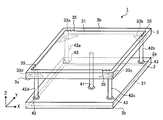
- FIG. 1 is a perspective view showing a configuration of an antenna device according to a first embodiment of the present invention.
- an antenna device 1 according to a first embodiment of the present invention includes a pair of dielectric substrates 2 and 3 formed in a quadrangular shape, and the pair of dielectric substrates 2 and 3 are spaced apart from each other by a predetermined distance. They are spaced apart from each other.
- the pair of dielectric substrates 2 and 3 are formed of a resin material such as glass epoxy resin.
- a ground conductor plate 21 formed of a sheet metal part is disposed on the back side 2b of the dielectric substrate 2.
- a radiation conductor plate 31 formed of copper foil or the like is disposed on the back surface 3a side of the dielectric substrate 3 facing the dielectric substrate 2.
- the radiating conductor plate 31 is formed with a slit-shaped perturbation portion 31c so that circularly polarized radio waves can be transmitted and received.
- a conductive member 41 erected on the surface 2 a side of the dielectric substrate 2 facing the dielectric substrate 3 is connected to the radiation conductor plate 31.
- a power supply signal supplied from a power supply pin (not shown) to the conductive member 41 is supplied to the radiation conductor plate 31 via the conductive member 41. That is, the radiating conductor plate 31 is directly fed by a one-point feeding method.
- the four triangular capacitance forming portions 33a, 33b, 33c, 33d formed by sheet metal parts are arranged. That is, the four capacitance forming portions 33a to 33d are provided at an interval of approximately 90 degrees with the center position of the dielectric substrate 3 (radiating conductor plate 31) as an axis.
- the four capacitance forming portions 33a to 33d are connected to one end portions of rod-like conductive members 42a, 42b, 42c, and 42d that penetrate the dielectric substrate 3.
- the other end portions of the conductive members 42 a to 42 d are fixed to the dielectric substrate 2 with a solder material 43.
- the conductive members 42a to 42d have a function of supporting the dielectric substrate 3 at a predetermined distance from the surface 2a of the dielectric substrate 2 and a function of grounding the capacitor forming portions 33a to 33d.
- the four capacitance forming portions 33 a to 33 d are electromagnetically coupled to the radiation conductor plate 31 to form a capacitive element between the radiation conductor plate 31.
- the resonance frequency of the antenna device 1 is lowered, and the antenna device 1 can be downsized.
- the capacity forming portions 33a to 33d for adjusting the resonance frequency of the antenna device 1 are the outermost surfaces of the antenna device 1. It is disposed on the surface side 3 b of the dielectric substrate 3. Therefore, according to such a configuration, even when the frequency characteristics of the antenna device 1 fluctuate due to fluctuations in the additional capacitance due to manufacturing variations in the dielectric constant of the dielectric substrate 3, as shown in FIG.
- the capacitance forming portions 33a to 33d By trimming the capacitance forming portions 33a to 33d, the opposing area of the capacitance forming portions 33a to 33d with respect to the radiation conductor plate 31 is adjusted, thereby easily adjusting the additional capacitance and changing the frequency characteristics of the antenna device 1 to the desired frequency characteristics. Can be adjusted.
- the capacitance forming portions 33a to 33d have a triangular shape.
- the capacitance forming portions 33a to 33d have a shape other than the triangular shape. May be.
- a plurality of protrusions 34 protruding in the in-plane direction of the surface 3b of the dielectric substrate 3 are provided in the capacitance forming parts 33a to 33d, and the length and number of the protrusions 34 to be trimmed are adjusted. Accordingly, the additional capacity may be adjusted.
- the radiating conductor plate 31 and the capacitance forming portions 33a to 33d are provided on the back surface 3a side and the front surface side 3b of the dielectric substrate 3, respectively.
- capacitance forming portions 33a to 33d and a radiating conductor plate 31 are provided on the back surface 3a side and the front surface side 3b of the dielectric substrate 3, respectively, and the radiating conductor plate 31 is trimmed to thereby form a capacitance forming portion 33a for the radiating conductor plate 31.
- the opposing area of ⁇ 33d may be adjusted.
- the dielectric substrate 3 is supported by the dielectric substrate 2, the conductive members 42a to 42d, and the capacitance forming portions 33a to 33d.
- protrusions 35 are provided at the four corners of the radiation conductor plate 31 facing the capacitor forming portions 33a to 33d, and the length and number of the protrusions 35 to be trimmed are adjusted.
- the facing area of the capacitance forming portions 33a to 33d with respect to the radiation conductor plate 31 is adjusted.
- FIG. 6 is a perspective view showing the configuration of the antenna device according to the second embodiment of the present invention.
- the antenna device 1 according to the second embodiment of the present invention includes a pair of dielectric substrates 2 and 3 formed in a quadrangular shape, and the pair of dielectric substrates 2 and 3 are spaced apart from each other by a predetermined distance. They are spaced apart from each other.
- the pair of dielectric substrates 2 and 3 are formed of a resin material such as glass epoxy resin.
- a ground conductor plate 21 formed of a sheet metal part is disposed on the back side 2b of the dielectric substrate 2.
- a Wilkinson distributor 22 is provided on the surface 2 a side of the dielectric substrate 2 facing the dielectric substrate 3.
- the Wilkinson distributor 22 has two output portions 22a and 22b which are in a positional relationship 90 degrees apart from each other within the surface 2a of the dielectric substrate 2.
- a power supply signal supplied from one power supply pin (not shown) to Wilkinson distributor 22 is output from output units 22a and 22b with the same amplitude and a phase difference of 90 degrees.
- the positions of the output units 22a and 22b may be adjusted by adjusting the pattern of the Wilkinson distributor 22.
- a radiation conductor plate 31 formed of copper foil or the like is disposed on the back surface 3a side of the dielectric substrate 3 facing the dielectric substrate 2.
- a pair of power supply pads 32a and 32b formed of a copper foil or the like is disposed on the surface side 3b of the dielectric substrate 3.
- the pair of power supply pads 32a and 32b are disposed at positions corresponding to the output portions 22a and 22b, respectively.
- the power supply pads 32 a and 32 b and the output portions 22 a and 22 b are electrically connected by rod-like conductive members 41 a and 41 b that penetrate the dielectric substrate 3.
- the power supply signals output from the output units 22a and 22b are supplied to the power supply pads 32a and 32b via the conductive members 41a and 41b, and are formed between the power supply pads 32a and 32b and the radiation conductor plate 31.
- Capacitive power is supplied to the radiation conductor plate 31 through the capacitive element. That is, the radiating conductor plate 31 is capacitively fed by a two-point feeding method.
- the pair of power supply pads 32a and 32b functions as a capacitive power supply unit according to the present invention.
- the four triangular capacitance forming portions 33a, 33b, 33c, 33d formed by sheet metal parts are arranged. That is, the four capacitance forming portions 33a to 33d are provided at an interval of approximately 90 degrees with the center position (radiation conductor plate 31) of the dielectric substrate 3 as an axis.
- the four capacitance forming portions 33a to 33d are connected to one end portions of rod-like conductive members 42a, 42b, 42c, and 42d that penetrate the dielectric substrate 3.
- the other end portions of the conductive members 42 a to 42 d are fixed to the ground conductor plate 21 with a solder material 43.
- the conductive members 42a to 42d have a function of supporting the dielectric substrate 3 at a predetermined distance from the surface 2a of the dielectric substrate 2 and a function of grounding the capacitor forming portions 33a to 33d.
- the four capacitance forming portions 33 a to 33 d are electromagnetically coupled to the radiation conductor plate 31 to form a capacitive element between the radiation conductor plate 31.
- the resonance frequency of the antenna device 1 is lowered, and the antenna device 1 can be downsized.
- the capacity forming portions 33a to 33d for adjusting the resonance frequency of the antenna device 1 are the outermost surfaces of the antenna device 1. It is disposed on the surface side 3 b of the dielectric substrate 3. Therefore, according to such a configuration, even when the frequency characteristics of the antenna device 1 fluctuate due to fluctuations in the additional capacitance due to manufacturing variations in the dielectric constant of the dielectric substrate 3, the capacitance forming portions 33a to 33d can be provided. By adjusting the opposing area of the capacitance forming portions 33a to 33d with respect to the radiation conductor plate 31 by trimming, the additional capacitance can be easily adjusted and the frequency characteristic of the antenna device 1 can be adjusted to a desired frequency characteristic.
- the radiation conductor plate 31 is fed by the two-point feeding method, so that the band of the antenna device 1 can be widened.
- the power feeding pads 32a and 32b are disposed on the surface side 3b of the dielectric substrate 3 which is the outermost surface of the antenna device 1, and therefore the power feeding pads 32a and 32b are arranged.
- the capacitance forming portions 33a to 33d and the radiation conductor plate 31 are disposed on the front surface 3b side and the back surface 3a side of the dielectric substrate 3, respectively.
- the capacitance forming portions 33a to 33d and the radiation conductor plate 31 may be disposed on the back surface 3a side and the front surface 3b side of the dielectric substrate 3, respectively.
- the additional capacitance is adjusted by trimming the radiation conductor plate 31 disposed on the outermost surface of the antenna device 1 to adjust the facing area of the radiation conductor plate 31 with respect to the capacitance forming portions 33a to 33d.
- the frequency characteristic of the antenna device 1 can be adjusted to a desired frequency characteristic.
- the dielectric substrate 3 is supported by the dielectric substrate 2, the conductive members 42a to 42d, and the capacitance forming portions 33a to 33d.
- the radiating conductor plate 31 and the capacitance forming portions 33a to 33d are provided on the back surface 3a side and the front surface side 3b of the dielectric substrate 3, respectively.
- capacitance forming portions 33a to 33d and a radiating conductor plate 31 are provided on the back surface 3a side and the front surface side 3b of the dielectric substrate 3, respectively, and the radiating conductor plate 31 is trimmed to thereby form a capacitance forming portion 33a for the radiating conductor plate 31.
- the opposing area of ⁇ 33d may be adjusted. Specifically, in this case, as shown in FIG.
- protrusions 35 are provided at the four corners of the radiation conductor plate 31 facing the capacitor forming portions 33a to 33d, and the length and number of the protrusions 35 to be trimmed are adjusted. Thus, the facing area of the capacitance forming portions 33a to 33d with respect to the radiation conductor plate 31 is adjusted.
- the area of the radiation conductor plate 31 is reduced, so that the power supply pads 32a and 32b are connected to the dielectric substrate.
- 3 is preferably provided on the back surface 3a side.
- the opening 44 may be formed in the radiation conductor plate 31 and the dielectric substrate 3 so that the mounting state of the Wilkinson distributor 22 can be confirmed.
- the power supply pads 32a and 32b are arranged on the front surface 3b side of the dielectric substrate 3.
- Cutout portions 31a and 31b may be formed by cutting out the radiation conductor plate 31 disposed on the side, and the power supply pads 32a and 32b may be disposed in the cutout portions 31a and 31b.
- the area of the radiating conductor plate 31 is reduced as compared with the configuration shown in FIG. 6, so that the antenna characteristics may be deteriorated.
- the radiating conductor plate 31 is disposed on the back surface 3a side of the dielectric substrate 3.
- the radiation conductor plate 31 may be arranged on the surface 3b side of the dielectric substrate 3 so as not to contact the portions 33a to 33d.
- pad portions 36a, 36b, 36c, and 36d instead of the capacitance forming portions 33a to 33d shown in FIG. 10, pad portions 36a, 36b, 36c, and 36d that are in contact with the conductive members 42a to 42d, the radiation conductor plate 31, and the pad portion.
- Capacitor chips 37a, 37b, 37c, and 37d that connect 36a to 36d may be provided. In the configuration shown in FIG.
- the capacitor chips 37a to 37d are replaced with other capacitor chips having different capacities.
- the additional capacity can be easily adjusted by appropriately changing to.
- the antenna device uses a satellite navigation system GALILEO of the Russian satellite navigation system GLONASS (Global Navigation Satellite System), the European Union (EU) and the European Space Agency (ESA), a satellite in the United States. It can be applied to SDARS (Satellite Digital Audio Radio Service) etc., which is a service by digital broadcasting. That is, other embodiments, examples, operational techniques, and the like made by those skilled in the art based on the present embodiment are all included in the scope of the present invention.
- GALILEO Global Navigation Satellite System
- GLONASS Global Navigation Satellite System
- EU European Union
- ESA European Space Agency
- the present invention can be used for a GPS antenna device and a composite antenna device including a GPS antenna device.
Abstract
Capacity forming parts (33a to 33d) for adjusting the resonant frequency of an antenna system (1) are arranged on a front surface (3b) of a dielectric substrate (3) that is the topmost surface of the antenna system (1). As a result, even if the frequency characteristics of the antenna system (1) vary with fluctuations in additional capacity due to manufacturing variations in the permittivity of the dielectric substrate (3), the additional capacity can be easily adjusted by adjusting the areas of the capacity forming parts (33a to 33d) facing a radiation conductor (31) through trimming of the capacity forming parts (33a to 33d), and the frequency characteristics of the antenna system (1) can be adjusted to desired frequency characteristics.
Description
本発明は、GPS用アンテナ装置やGPS用アンテナ装置を含む複合アンテナ装置に利用して好適なアンテナ装置に関するものである。
The present invention relates to an antenna device suitable for use in a GPS antenna device or a composite antenna device including a GPS antenna device.
近年、自動車に搭載される車載用情報機器として、GPS(衛星測位システム:Global Positioning System)やVICS(道路交通情報通信システム:Vehicle Information and Communication System)を利用したナビゲーション装置、ETC(自動料金収受システム:Electronic Toll Collection system)を利用した有料道路における料金自動支払システムなどの普及が目覚ましい。また、車載電話システムとGPSとを併用して事故発生時などに災害救助信号を自動発信する緊急通信システムも実用化されている。これらの車載用情報機器において用いられるアンテナ装置については、自動車の限られた空きスペースに配置されることから、小型であることが求められる。このため、車載用情報機器では、平面アンテナ装置がアンテナ装置として広く利用されている。特にGPS用やETC用のアンテナ装置については、円偏波の電波を送受信する関係から平面アンテナ装置が多用されている。
In recent years, navigation devices using GPS (Global Positioning System) and VICS (Vehicle Information and Communication System), ETC (Automatic Toll Collection System) as in-vehicle information devices installed in automobiles : The automatic toll payment system on toll roads using the Electronic Toll Collection system is remarkable. In addition, an emergency communication system that automatically uses a vehicle-mounted telephone system and GPS to automatically transmit a disaster rescue signal when an accident occurs has been put into practical use. The antenna device used in these in-vehicle information devices is required to be small because it is disposed in a limited space of the automobile. For this reason, in a vehicle information device, a planar antenna device is widely used as an antenna device. In particular, for GPS and ETC antenna devices, planar antenna devices are frequently used because of the transmission and reception of circularly polarized radio waves.
従来の平面アンテナ装置として、接地導体上に設けられた誘電体基板と、誘電体基板上に配設された複数の半田ランドと、誘電体基板上に所定間隔離間して配置された放射導体板と、放射導体板の中央部を除く複数箇所を誘電体基板側へ折り返して形成された複数の脚片とを備え、複数の脚片を半田ランドに半田付けして放射導体板を支持する構成を有するものが知られている。このような構成を有する平面アンテナ装置では、半田ランドが誘電体基板を介して接地導体と対向している。このため、半田ランドに半田付けされている脚片と接地導体との間に容量が付加されることによって、共振周波数が低くなり、結果として、放射導体板及び平面アンテナ装置の小型化を実現することができる。
As a conventional planar antenna device, a dielectric substrate provided on a ground conductor, a plurality of solder lands provided on the dielectric substrate, and a radiation conductor plate arranged on the dielectric substrate at a predetermined interval And a plurality of leg pieces formed by folding a plurality of locations excluding the central portion of the radiating conductor plate toward the dielectric substrate, and supporting the radiating conductor plate by soldering the plurality of leg pieces to a solder land. Are known. In the planar antenna device having such a configuration, the solder land is opposed to the ground conductor via the dielectric substrate. For this reason, by adding a capacitance between the leg piece soldered to the solder land and the ground conductor, the resonance frequency is lowered, and as a result, the radiation conductor plate and the planar antenna device can be miniaturized. be able to.
ところが、このような平面アンテナ装置の構成によれば、小型化を実現することはできるが、半田ランドの半田量や半田付け面積のばらつきによって付加容量が変動し、結果として、平面アンテナ装置の周波数特性が変動することがある。このため、特許文献1,2には、誘電体基板に対向する脚片の先端部を折り曲げたり、脚片と接地導体との間にコンデンサ素子を設けたりするなどして、半田ランドを用いることなく脚片と接地導体との間に容量を付加する方法が提案されている。
However, according to such a configuration of the planar antenna device, it is possible to reduce the size, but the additional capacitance varies due to variations in the solder land solder amount and the soldering area, resulting in the frequency of the planar antenna device. Characteristics may vary. For this reason, in Patent Documents 1 and 2, the solder land is used by bending the tip of the leg piece facing the dielectric substrate or by providing a capacitor element between the leg piece and the ground conductor. Instead, a method of adding a capacitance between the leg piece and the ground conductor has been proposed.
しかしながら、特許文献1,2記載の平面アンテナ装置では、脚片の折り曲げ部やコンデンサなどの容量形成成分は、誘電体基板側に配置されているために、組み付け後にその容量値を調整することは難しい。このため、特許文献1,2記載の平面アンテナ装置によれば、誘電体基板の誘電率の製造ばらつきによって付加容量が変動することにより平面アンテナ装置の周波数特性が変動した場合に、付加容量を調整することによって平面アンテナ装置の周波数特性を調整することが困難であった。
However, in the planar antenna devices described in Patent Documents 1 and 2, since the capacitance forming components such as the bent portions of the leg pieces and the capacitors are arranged on the dielectric substrate side, it is not possible to adjust the capacitance value after assembly. difficult. Therefore, according to the planar antenna device described in Patent Documents 1 and 2, the additional capacitance is adjusted when the frequency characteristics of the planar antenna device fluctuate due to fluctuations in the additional capacitance due to manufacturing variations in the dielectric constant of the dielectric substrate. This makes it difficult to adjust the frequency characteristics of the planar antenna device.
本発明は、上記課題に鑑みてなされたものであって、その目的は、付加容量の調整が容易なアンテナ装置を提供することにある。
The present invention has been made in view of the above problems, and an object of the present invention is to provide an antenna device in which an additional capacity can be easily adjusted.
上記課題を解決し、目的を達成するために、本発明の第1の態様に係るアンテナ装置は、接地導体板を有する接地基板と、前記接地基板の表面から所定間隔離間して配置された樹脂基板と、前記樹脂基板の前記接地基板に対向する裏面側又は表面側に設けられた放射導体板と、前記放射導体板が設けられている前記樹脂基板の面内に設けられた、該放射導体板と電磁結合して該放射導体板との間に容量素子を形成する容量形成部と、を備える。
In order to solve the above problems and achieve the object, an antenna device according to a first aspect of the present invention includes a grounding substrate having a grounding conductor plate and a resin disposed at a predetermined distance from the surface of the grounding substrate. A radiation conductor plate provided on a back surface or a front surface side of the resin substrate facing the grounding substrate, and the radiation conductor provided in a plane of the resin substrate on which the radiation conductor plate is provided. And a capacitance forming portion that electromagnetically couples with the plate to form a capacitive element between the radiation conductor plate.
上記課題を解決し、目的を達成するために、本発明の第2の態様に係るアンテナ装置は、接地導体板を有する接地基板と、前記接地基板の表面から所定間隔離間して配置された樹脂基板と、前記樹脂基板の前記接地基板に対向する裏面側又は表面側に設けられた放射導体板と、前記放射導体板が設けられている前記樹脂基板の面に対向する面内に設けられた、該放射導体板と電磁結合して該放射導体板との間に容量素子を形成する容量形成部と、を備える。
In order to solve the above problems and achieve the object, an antenna device according to a second aspect of the present invention includes a grounding substrate having a grounding conductor plate, and a resin disposed at a predetermined distance from the surface of the grounding substrate. A substrate, a radiation conductor plate provided on the back surface or the surface side of the resin substrate facing the ground substrate, and a surface facing the surface of the resin substrate on which the radiation conductor plate is provided. And a capacitance forming part that electromagnetically couples with the radiation conductor plate and forms a capacitive element between the radiation conductor plate.
本発明に係るアンテナ装置によれば、接地基板及び樹脂基板の誘電率の製造ばらつきによって付加容量が変動した場合であっても、付加容量を容易に調整することができる。
The antenna device according to the present invention can easily adjust the additional capacitance even when the additional capacitance varies due to manufacturing variations in the dielectric constant of the ground substrate and the resin substrate.
以下、図面を参照して、本発明の第1及び第2の実施形態であるアンテナ装置の構成について説明する。
Hereinafter, the configuration of the antenna device according to the first and second embodiments of the present invention will be described with reference to the drawings.
第1の実施形態
始めに、図1乃至図5を参照して、本発明の第1の実施形態であるアンテナ装置の構成について説明する。 First Embodiment First, the configuration of an antenna device according to a first embodiment of the present invention will be described with reference to FIGS. 1 to 5.
始めに、図1乃至図5を参照して、本発明の第1の実施形態であるアンテナ装置の構成について説明する。 First Embodiment First, the configuration of an antenna device according to a first embodiment of the present invention will be described with reference to FIGS. 1 to 5.
図1は、本発明の第1の実施形態であるアンテナ装置の構成を示す斜視図である。図1に示すように、本発明の第1の実施形態であるアンテナ装置1は、四角形状に形成された一対の誘電体基板2,3を備え、一対の誘電体基板2,3は所定間隔離間して対向配置されている。一対の誘電体基板2,3は、ガラスエポキシ樹脂などの樹脂材料によって形成されている。
FIG. 1 is a perspective view showing a configuration of an antenna device according to a first embodiment of the present invention. As shown in FIG. 1, an antenna device 1 according to a first embodiment of the present invention includes a pair of dielectric substrates 2 and 3 formed in a quadrangular shape, and the pair of dielectric substrates 2 and 3 are spaced apart from each other by a predetermined distance. They are spaced apart from each other. The pair of dielectric substrates 2 and 3 are formed of a resin material such as glass epoxy resin.
誘電体基板2の裏面側2bには板金部品によって形成された接地導体板21が配置されている。誘電体基板3の誘電体基板2と対向する裏面3a側には、銅箔などによって形成された放射導体板31が配置されている。放射導体板31には、円偏波の電波を送受信可能なようにスリット形状の摂動部31cが形成されている。放射導体板31には、誘電体基板2の誘電体基板3と対向する表面2a側に立設された導電性部材41が接続されている。図示しない給電ピンから導電性部材41に供給された給電信号は、導電性部材41を介して放射導体板31に供給される。すなわち、放射導体板31は1点給電方式によって直接給電される。
A ground conductor plate 21 formed of a sheet metal part is disposed on the back side 2b of the dielectric substrate 2. A radiation conductor plate 31 formed of copper foil or the like is disposed on the back surface 3a side of the dielectric substrate 3 facing the dielectric substrate 2. The radiating conductor plate 31 is formed with a slit-shaped perturbation portion 31c so that circularly polarized radio waves can be transmitted and received. A conductive member 41 erected on the surface 2 a side of the dielectric substrate 2 facing the dielectric substrate 3 is connected to the radiation conductor plate 31. A power supply signal supplied from a power supply pin (not shown) to the conductive member 41 is supplied to the radiation conductor plate 31 via the conductive member 41. That is, the radiating conductor plate 31 is directly fed by a one-point feeding method.
誘電体基板3の表面側3bの四隅には、板金部品によって形成された三角形状の4つの容量形成部33a,33b,33c,33dが配置されている。すなわち、4つの容量形成部33a~33dは、誘電体基板3(放射導体板31)の中心位置を軸として略90度間隔に設けられている。4つの容量形成部33a~33dは、誘電体基板3を貫通する棒状の導電性部材42a,42b,42c,42dの一端部に接続されている。導電性部材42a~42dの他端部は、半田材料43によって誘電体基板2に固定されている。導電性部材42a~42dは、誘電体基板3を誘電体基板2の表面2aから所定間隔離間して支持する機能と共に、容量形成部33a~33dを接地する機能を有する。これにより、4つの容量形成部33a~33dは、放射導体板31と電磁結合して放射導体板31との間に容量素子を形成する。この結果、アンテナ装置1の共振周波数が低くなり、アンテナ装置1の小型化を実現することができる。
At the four corners on the surface side 3b of the dielectric substrate 3, four triangular capacitance forming portions 33a, 33b, 33c, 33d formed by sheet metal parts are arranged. That is, the four capacitance forming portions 33a to 33d are provided at an interval of approximately 90 degrees with the center position of the dielectric substrate 3 (radiating conductor plate 31) as an axis. The four capacitance forming portions 33a to 33d are connected to one end portions of rod-like conductive members 42a, 42b, 42c, and 42d that penetrate the dielectric substrate 3. The other end portions of the conductive members 42 a to 42 d are fixed to the dielectric substrate 2 with a solder material 43. The conductive members 42a to 42d have a function of supporting the dielectric substrate 3 at a predetermined distance from the surface 2a of the dielectric substrate 2 and a function of grounding the capacitor forming portions 33a to 33d. Thus, the four capacitance forming portions 33 a to 33 d are electromagnetically coupled to the radiation conductor plate 31 to form a capacitive element between the radiation conductor plate 31. As a result, the resonance frequency of the antenna device 1 is lowered, and the antenna device 1 can be downsized.
以上の説明から明らかなように、本発明の第1の実施形態であるアンテナ装置1では、アンテナ装置1の共振周波数を調整するための容量形成部33a~33dがアンテナ装置1の最表面である誘電体基板3の表面側3bに配置されている。従って、このような構成によれば、誘電体基板3の誘電率の製造ばらつきによって付加容量が変動することによりアンテナ装置1の周波数特性が変動した場合であっても、例えば図2に示すように容量形成部33a~33dをトリミングすることによって放射導体板31に対する容量形成部33a~33dの対向面積を調整することにより、付加容量を容易に調整し、アンテナ装置1の周波数特性を所望の周波数特性に調整することができる。
As is apparent from the above description, in the antenna device 1 according to the first embodiment of the present invention, the capacity forming portions 33a to 33d for adjusting the resonance frequency of the antenna device 1 are the outermost surfaces of the antenna device 1. It is disposed on the surface side 3 b of the dielectric substrate 3. Therefore, according to such a configuration, even when the frequency characteristics of the antenna device 1 fluctuate due to fluctuations in the additional capacitance due to manufacturing variations in the dielectric constant of the dielectric substrate 3, as shown in FIG. By trimming the capacitance forming portions 33a to 33d, the opposing area of the capacitance forming portions 33a to 33d with respect to the radiation conductor plate 31 is adjusted, thereby easily adjusting the additional capacitance and changing the frequency characteristics of the antenna device 1 to the desired frequency characteristics. Can be adjusted.
なお、本発明の第1の実施形態であるアンテナ装置1では、容量形成部33a~33dの形状は三角形状であるとしたが、容量形成部33a~33dの形状は三角形状以外の形状であってもよい。例えば、図3に示すように、誘電体基板3の表面3bの面内方向に突出する複数の突起部34を容量形成部33a~33dに設け、トリミングする突起部34の長さや本数を調整することによって、付加容量を調整するようにしてもよい。
In the antenna device 1 according to the first embodiment of the present invention, the capacitance forming portions 33a to 33d have a triangular shape. However, the capacitance forming portions 33a to 33d have a shape other than the triangular shape. May be. For example, as shown in FIG. 3, a plurality of protrusions 34 protruding in the in-plane direction of the surface 3b of the dielectric substrate 3 are provided in the capacitance forming parts 33a to 33d, and the length and number of the protrusions 34 to be trimmed are adjusted. Accordingly, the additional capacity may be adjusted.
また、本発明の第1の実施形態であるアンテナ装置1では、誘電体基板3の裏面3a側及び表面側3bにそれぞれ放射導体板31及び容量形成部33a~33dを設けたが、図4に示すように、誘電体基板3の裏面3a側及び表面側3bにそれぞれ容量形成部33a~33d及び放射導体板31を設け、放射導体板31をトリミングすることによって放射導体板31に対する容量形成部33a~33dの対向面積を調整するようにしてもよい。誘電体基板3は、誘電体基板2,導電性部材42a~42d,及び容量形成部33a~33dによって支持されている。具体的には、この場合、図5に示すように、容量形成部33a~33dに対向する放射導体板31の4隅に突起部35を設け、トリミングする突起部35の長さや本数を調整することによって、放射導体板31に対する容量形成部33a~33dの対向面積を調整する。
In the antenna device 1 according to the first embodiment of the present invention, the radiating conductor plate 31 and the capacitance forming portions 33a to 33d are provided on the back surface 3a side and the front surface side 3b of the dielectric substrate 3, respectively. As shown, capacitance forming portions 33a to 33d and a radiating conductor plate 31 are provided on the back surface 3a side and the front surface side 3b of the dielectric substrate 3, respectively, and the radiating conductor plate 31 is trimmed to thereby form a capacitance forming portion 33a for the radiating conductor plate 31. The opposing area of ~ 33d may be adjusted. The dielectric substrate 3 is supported by the dielectric substrate 2, the conductive members 42a to 42d, and the capacitance forming portions 33a to 33d. Specifically, in this case, as shown in FIG. 5, protrusions 35 are provided at the four corners of the radiation conductor plate 31 facing the capacitor forming portions 33a to 33d, and the length and number of the protrusions 35 to be trimmed are adjusted. Thus, the facing area of the capacitance forming portions 33a to 33d with respect to the radiation conductor plate 31 is adjusted.
第2の実施形態
次に、図6乃至図11を参照して、本発明の第2の実施形態であるアンテナ装置の構成について説明する。 Second Embodiment Next, a configuration of an antenna device according to a second embodiment of the present invention will be described with reference to FIGS.
次に、図6乃至図11を参照して、本発明の第2の実施形態であるアンテナ装置の構成について説明する。 Second Embodiment Next, a configuration of an antenna device according to a second embodiment of the present invention will be described with reference to FIGS.
図6は、本発明の第2の実施形態であるアンテナ装置の構成を示す斜視図である。図6に示すように、本発明の第2の実施形態であるアンテナ装置1は、四角形状に形成された一対の誘電体基板2,3を備え、一対の誘電体基板2,3は所定間隔離間して対向配置されている。一対の誘電体基板2,3は、ガラスエポキシ樹脂などの樹脂材料によって形成されている。
FIG. 6 is a perspective view showing the configuration of the antenna device according to the second embodiment of the present invention. As shown in FIG. 6, the antenna device 1 according to the second embodiment of the present invention includes a pair of dielectric substrates 2 and 3 formed in a quadrangular shape, and the pair of dielectric substrates 2 and 3 are spaced apart from each other by a predetermined distance. They are spaced apart from each other. The pair of dielectric substrates 2 and 3 are formed of a resin material such as glass epoxy resin.
誘電体基板2の裏面側2bには板金部品によって形成された接地導体板21が配置されている。誘電体基板2の誘電体基板3と対向する表面2a側には、ウィルキンソン型分配器22が設けられている。ウィルキンソン型分配器22は、誘電体基板2の表面2aの面内で互いに90度離れた位置関係にある2つの出力部22a,22bを有する。図示しない1本の給電ピンからウィルキンソン型分配器22に供給された給電信号は、同振幅で90度の位相差を持って出力部22a,22bからそれぞれ出力される。ウィルキンソン型分配器22を用いることにより、図示しない受信回路とのインタフェイスを1本の給電ピンのみとすることができる。なお、ウィルキンソン型分配器22のパターンを調整することによって出力部22a,22bの位置を調整してもよい。
A ground conductor plate 21 formed of a sheet metal part is disposed on the back side 2b of the dielectric substrate 2. A Wilkinson distributor 22 is provided on the surface 2 a side of the dielectric substrate 2 facing the dielectric substrate 3. The Wilkinson distributor 22 has two output portions 22a and 22b which are in a positional relationship 90 degrees apart from each other within the surface 2a of the dielectric substrate 2. A power supply signal supplied from one power supply pin (not shown) to Wilkinson distributor 22 is output from output units 22a and 22b with the same amplitude and a phase difference of 90 degrees. By using the Wilkinson distributor 22, it is possible to use only one power supply pin as an interface with a receiving circuit (not shown). The positions of the output units 22a and 22b may be adjusted by adjusting the pattern of the Wilkinson distributor 22.
誘電体基板3の誘電体基板2と対向する裏面3a側には、銅箔などによって形成された放射導体板31が配置されている。誘電体基板3の表面側3bには、銅箔などによって形成された一対の給電パッド32a,32bが配置されている。一対の給電パッド32a,32bはそれぞれ、出力部22a,22bに対応する位置に配置されている。給電パッド32a,32bと出力部22a,22bとは、誘電体基板3を貫通する棒状の導電性部材41a,41bによって電気的に接続されている。これにより、出力部22a,22bから出力された給電信号は、導電性部材41a,41bを介して給電パッド32a,32bに供給され、給電パッド32a,32bと放射導体板31との間に形成される容量素子を介して放射導体板31に容量給電されることになる。すなわち、放射導体板31は2点給電方式によって容量給電される。一対の給電パッド32a,32bは、本発明に係る容量給電部として機能する。
On the back surface 3a side of the dielectric substrate 3 facing the dielectric substrate 2, a radiation conductor plate 31 formed of copper foil or the like is disposed. On the surface side 3b of the dielectric substrate 3, a pair of power supply pads 32a and 32b formed of a copper foil or the like is disposed. The pair of power supply pads 32a and 32b are disposed at positions corresponding to the output portions 22a and 22b, respectively. The power supply pads 32 a and 32 b and the output portions 22 a and 22 b are electrically connected by rod-like conductive members 41 a and 41 b that penetrate the dielectric substrate 3. Thus, the power supply signals output from the output units 22a and 22b are supplied to the power supply pads 32a and 32b via the conductive members 41a and 41b, and are formed between the power supply pads 32a and 32b and the radiation conductor plate 31. Capacitive power is supplied to the radiation conductor plate 31 through the capacitive element. That is, the radiating conductor plate 31 is capacitively fed by a two-point feeding method. The pair of power supply pads 32a and 32b functions as a capacitive power supply unit according to the present invention.
誘電体基板3の表面側3bの四隅には、板金部品によって形成された三角形状の4つの容量形成部33a,33b,33c,33dが配置されている。すなわち、4つの容量形成部33a~33dは、誘電体基板3の中心位置(放射導体板31)を軸として略90度間隔に設けられている。4つの容量形成部33a~33dは、誘電体基板3を貫通する棒状の導電性部材42a,42b,42c,42dの一端部に接続されている。導電性部材42a~42dの他端部は、半田材料43によって接地導体板21に固定されている。導電性部材42a~42dは、誘電体基板3を誘電体基板2の表面2aから所定間隔離間して支持する機能と共に、容量形成部33a~33dを接地する機能を有する。これにより、4つの容量形成部33a~33dは、放射導体板31と電磁結合して放射導体板31との間に容量素子を形成する。この結果、アンテナ装置1の共振周波数が低くなり、アンテナ装置1の小型化を実現することができる。
At the four corners on the surface side 3b of the dielectric substrate 3, four triangular capacitance forming portions 33a, 33b, 33c, 33d formed by sheet metal parts are arranged. That is, the four capacitance forming portions 33a to 33d are provided at an interval of approximately 90 degrees with the center position (radiation conductor plate 31) of the dielectric substrate 3 as an axis. The four capacitance forming portions 33a to 33d are connected to one end portions of rod-like conductive members 42a, 42b, 42c, and 42d that penetrate the dielectric substrate 3. The other end portions of the conductive members 42 a to 42 d are fixed to the ground conductor plate 21 with a solder material 43. The conductive members 42a to 42d have a function of supporting the dielectric substrate 3 at a predetermined distance from the surface 2a of the dielectric substrate 2 and a function of grounding the capacitor forming portions 33a to 33d. Thus, the four capacitance forming portions 33 a to 33 d are electromagnetically coupled to the radiation conductor plate 31 to form a capacitive element between the radiation conductor plate 31. As a result, the resonance frequency of the antenna device 1 is lowered, and the antenna device 1 can be downsized.
以上の説明から明らかなように、本発明の第2の実施形態であるアンテナ装置1では、アンテナ装置1の共振周波数を調整するための容量形成部33a~33dがアンテナ装置1の最表面である誘電体基板3の表面側3bに配置されている。従って、このような構成によれば、誘電体基板3の誘電率の製造ばらつきによって付加容量が変動することによりアンテナ装置1の周波数特性が変動した場合であっても、容量形成部33a~33dをトリミングすることによって放射導体板31に対する容量形成部33a~33dの対向面積を調整することにより、付加容量を容易に調整し、アンテナ装置1の周波数特性を所望の周波数特性に調整することができる。
As is clear from the above description, in the antenna device 1 according to the second embodiment of the present invention, the capacity forming portions 33a to 33d for adjusting the resonance frequency of the antenna device 1 are the outermost surfaces of the antenna device 1. It is disposed on the surface side 3 b of the dielectric substrate 3. Therefore, according to such a configuration, even when the frequency characteristics of the antenna device 1 fluctuate due to fluctuations in the additional capacitance due to manufacturing variations in the dielectric constant of the dielectric substrate 3, the capacitance forming portions 33a to 33d can be provided. By adjusting the opposing area of the capacitance forming portions 33a to 33d with respect to the radiation conductor plate 31 by trimming, the additional capacitance can be easily adjusted and the frequency characteristic of the antenna device 1 can be adjusted to a desired frequency characteristic.
また、本発明の第2の実施形態であるアンテナ装置1では、放射導体板31は2点給電方式によって給電されるので、アンテナ装置1の帯域を広帯域化することができる。また、本発明の一実施形態であるアンテナ装置1では、給電パッド32a,32bがアンテナ装置1の最表面である誘電体基板3の表面側3bに配置されているので、給電パッド32a,32bをトリミングすることによって放射導体板31に対する給電パッド32a,32bの対向面積を調整することにより、給電の際のインピーダンスを容易に調整することができる。
In the antenna device 1 according to the second embodiment of the present invention, the radiation conductor plate 31 is fed by the two-point feeding method, so that the band of the antenna device 1 can be widened. In the antenna device 1 according to the embodiment of the present invention, the power feeding pads 32a and 32b are disposed on the surface side 3b of the dielectric substrate 3 which is the outermost surface of the antenna device 1, and therefore the power feeding pads 32a and 32b are arranged. By adjusting the opposing area of the power supply pads 32a and 32b with respect to the radiation conductor plate 31 by trimming, the impedance at the time of power supply can be easily adjusted.
なお、本発明の第2の実施形態であるアンテナ装置1では、容量形成部33a~33d及び放射導体板31はそれぞれ誘電体基板3の表面3b側及び裏面3a側に配設されているが、図7に示すように、容量形成部33a~33d及び放射導体板31をそれぞれ誘電体基板3の裏面3a側及び表面3b側に配設するようにしてもよい。この図7に示す構成では、アンテナ装置1の最表面に配設された放射導体板31をトリミングすることによって容量形成部33a~33dに対する放射導体板31の対向面積を調整することにより、付加容量を容易に調整し、アンテナ装置1の周波数特性を所望の周波数特性に調整することができる。誘電体基板3は、誘電体基板2,導電性部材42a~42d,及び容量形成部33a~33dによって支持されている。
In the antenna device 1 according to the second embodiment of the present invention, the capacitance forming portions 33a to 33d and the radiation conductor plate 31 are disposed on the front surface 3b side and the back surface 3a side of the dielectric substrate 3, respectively. As shown in FIG. 7, the capacitance forming portions 33a to 33d and the radiation conductor plate 31 may be disposed on the back surface 3a side and the front surface 3b side of the dielectric substrate 3, respectively. In the configuration shown in FIG. 7, the additional capacitance is adjusted by trimming the radiation conductor plate 31 disposed on the outermost surface of the antenna device 1 to adjust the facing area of the radiation conductor plate 31 with respect to the capacitance forming portions 33a to 33d. The frequency characteristic of the antenna device 1 can be adjusted to a desired frequency characteristic. The dielectric substrate 3 is supported by the dielectric substrate 2, the conductive members 42a to 42d, and the capacitance forming portions 33a to 33d.
また、本発明の第2の実施形態であるアンテナ装置1では、誘電体基板3の裏面3a側及び表面側3bにそれぞれ放射導体板31及び容量形成部33a~33dを設けたが、図8に示すように、誘電体基板3の裏面3a側及び表面側3bにそれぞれ容量形成部33a~33d及び放射導体板31を設け、放射導体板31をトリミングすることによって放射導体板31に対する容量形成部33a~33dの対向面積を調整するようにしてもよい。具体的には、この場合、図5に示すように、容量形成部33a~33dに対向する放射導体板31の4隅に突起部35を設け、トリミングする突起部35の長さや本数を調整することによって、放射導体板31に対する容量形成部33a~33dの対向面積を調整する。
In the antenna device 1 according to the second embodiment of the present invention, the radiating conductor plate 31 and the capacitance forming portions 33a to 33d are provided on the back surface 3a side and the front surface side 3b of the dielectric substrate 3, respectively. As shown, capacitance forming portions 33a to 33d and a radiating conductor plate 31 are provided on the back surface 3a side and the front surface side 3b of the dielectric substrate 3, respectively, and the radiating conductor plate 31 is trimmed to thereby form a capacitance forming portion 33a for the radiating conductor plate 31. The opposing area of ~ 33d may be adjusted. Specifically, in this case, as shown in FIG. 5, protrusions 35 are provided at the four corners of the radiation conductor plate 31 facing the capacitor forming portions 33a to 33d, and the length and number of the protrusions 35 to be trimmed are adjusted. Thus, the facing area of the capacitance forming portions 33a to 33d with respect to the radiation conductor plate 31 is adjusted.
なお、図8に示す構成によれば、誘電体基板3の表面3b側に給電パッド32a,32bを設けた場合、放射導体板31の面積が小さくなるので、給電パッド32a,32bを誘電体基板3の裏面3a側に設けることが望ましい。また、ウィルキンソン型分配器22の実装状態を確認できるように、放射導体板31及び誘電体基板3に開口部44を形成してもよい。
According to the configuration shown in FIG. 8, when the power supply pads 32a and 32b are provided on the surface 3b side of the dielectric substrate 3, the area of the radiation conductor plate 31 is reduced, so that the power supply pads 32a and 32b are connected to the dielectric substrate. 3 is preferably provided on the back surface 3a side. Further, the opening 44 may be formed in the radiation conductor plate 31 and the dielectric substrate 3 so that the mounting state of the Wilkinson distributor 22 can be confirmed.
また、本発明の第2の実施形態であるアンテナ装置1では、給電パッド32a,32bを誘電体基板3の表面3b側に配置したが、図9に示すように、誘電体基板3の裏面3a側に配置されている放射導体板31を切り欠くことによって切り欠き部31a,31bを形成し、この切り欠き部31a,31bに給電パッド32a,32bを配置するようにしてもよい。但し、このような構成によれば、図6に示す構成と比較して放射導体板31の面積が狭くなるので、アンテナ特性が低下する可能性がある。
In the antenna device 1 according to the second embodiment of the present invention, the power supply pads 32a and 32b are arranged on the front surface 3b side of the dielectric substrate 3. However, as shown in FIG. Cutout portions 31a and 31b may be formed by cutting out the radiation conductor plate 31 disposed on the side, and the power supply pads 32a and 32b may be disposed in the cutout portions 31a and 31b. However, according to such a configuration, the area of the radiating conductor plate 31 is reduced as compared with the configuration shown in FIG. 6, so that the antenna characteristics may be deteriorated.
また、本発明の第2の実施形態であるアンテナ装置1では、放射導体板31を誘電体基板3の裏面3a側に配置したが、図10に示すように、給電パッド32a,32b及び容量形成部33a~33dと接触しないようにして誘電体基板3の表面3b側に放射導体板31を配置してもよい。また、図11に示すように、図10に示す容量形成部33a~33dの代わりに、導電性部材42a~42dと接触するパッド部36a,36b,36c,36dと、放射導体板31とパッド部36a~36dとを接続するコンデンサチップ37a,37b,37c,37dとを設けてもよい。この図8に示す構成では、誘電体基板3の誘電率の製造ばらつきによって付加容量が変動することによりアンテナ装置1の周波数特性が変動した場合、コンデンサチップ37a~37dを容量が異なる他のコンデンサチップに適宜付け替えることによって、付加容量を容易に調整することができる。
In the antenna device 1 according to the second embodiment of the present invention, the radiating conductor plate 31 is disposed on the back surface 3a side of the dielectric substrate 3. However, as shown in FIG. The radiation conductor plate 31 may be arranged on the surface 3b side of the dielectric substrate 3 so as not to contact the portions 33a to 33d. Further, as shown in FIG. 11, instead of the capacitance forming portions 33a to 33d shown in FIG. 10, pad portions 36a, 36b, 36c, and 36d that are in contact with the conductive members 42a to 42d, the radiation conductor plate 31, and the pad portion. Capacitor chips 37a, 37b, 37c, and 37d that connect 36a to 36d may be provided. In the configuration shown in FIG. 8, when the frequency characteristics of the antenna device 1 fluctuate due to fluctuations in the additional capacitance due to manufacturing variations in the dielectric constant of the dielectric substrate 3, the capacitor chips 37a to 37d are replaced with other capacitor chips having different capacities. The additional capacity can be easily adjusted by appropriately changing to.
以上、本発明者によってなされた発明を適用した実施の形態について説明したが、本実施形態による本発明の開示の一部をなす記述及び図面により本発明は限定されることはない。例えば、本発明に係るアンテナ装置は、ロシアの衛星航法システムGLONASS(Global Navigation Satellite System),欧州連合(EU)及び欧州宇宙機関(ESA: European Space Agency)による衛星航法システムGALILEO,米国における衛星を使用したデジタル放送によるサービスSDARS(Satellite Digital Audio Radio Service)等に適用できる。すなわち、本実施形態に基づいて当業者などによりなされる他の実施の形態、実施例及び運用技術などは全て本発明の範疇に含まれる。
As mentioned above, although the embodiment to which the invention made by the present inventor is applied has been described, the present invention is not limited by the description and the drawings that form part of the disclosure of the present invention according to this embodiment. For example, the antenna device according to the present invention uses a satellite navigation system GALILEO of the Russian satellite navigation system GLONASS (Global Navigation Satellite System), the European Union (EU) and the European Space Agency (ESA), a satellite in the United States. It can be applied to SDARS (Satellite Digital Audio Radio Service) etc., which is a service by digital broadcasting. That is, other embodiments, examples, operational techniques, and the like made by those skilled in the art based on the present embodiment are all included in the scope of the present invention.
本発明は、GPS用アンテナ装置やGPS用アンテナ装置を含む複合アンテナ装置に利用することができる。
The present invention can be used for a GPS antenna device and a composite antenna device including a GPS antenna device.
1 アンテナ装置
2,3 誘電体基板
21 接地導体板
22 ウィルキンソン型分配器
22a,22b 出力部
31 放射導体板
31a,31b 切り欠き部
32a,32b 給電パッド
33a,33b,33c,33d 容量形成部
34,35 突起部
36a,36b,36c,36d パッド部
37a,37b,37c,37d コンデンサチップ
41a,41b,42a,42b,42c,42d 導電性部材
44 開口部 DESCRIPTION OFSYMBOLS 1 Antenna apparatus 2, 3 Dielectric board | substrate 21 Grounding conductor plate 22 Wilkinson type | mold divider | distributor 22a, 22b Output part 31 Radiation conductor plate 31a, 31b Notch part 32a, 32b Feeding pad 33a, 33b, 33c, 33d Capacitance formation part 34, 35 Protrusions 36a, 36b, 36c, 36d Pad portions 37a, 37b, 37c, 37d Capacitor chips 41a, 41b, 42a, 42b, 42c, 42d Conductive members 44 Openings
2,3 誘電体基板
21 接地導体板
22 ウィルキンソン型分配器
22a,22b 出力部
31 放射導体板
31a,31b 切り欠き部
32a,32b 給電パッド
33a,33b,33c,33d 容量形成部
34,35 突起部
36a,36b,36c,36d パッド部
37a,37b,37c,37d コンデンサチップ
41a,41b,42a,42b,42c,42d 導電性部材
44 開口部 DESCRIPTION OF
Claims (11)
- 接地導体板を有する接地基板と、
前記接地基板の表面から所定間隔離間して配置された樹脂基板と、
前記樹脂基板の前記接地基板に対向する裏面側又は表面側に設けられた放射導体板と、
前記放射導体板が設けられている前記樹脂基板の面内に設けられた、該放射導体板と電磁結合して該放射導体板との間に容量素子を形成する容量形成部と、
を備えることを特徴とするアンテナ装置。 A grounding substrate having a grounding conductor plate;
A resin substrate disposed at a predetermined distance from the surface of the ground substrate;
A radiation conductor plate provided on the back side or the front side of the resin substrate facing the ground substrate;
A capacitance forming portion that is provided in a plane of the resin substrate on which the radiation conductor plate is provided, and that forms a capacitive element between the radiation conductor plate by electromagnetic coupling with the radiation conductor plate;
An antenna device comprising: - 接地導体板を有する接地基板と、
前記接地基板の表面から所定間隔離間して配置された樹脂基板と、
前記樹脂基板の前記接地基板に対向する裏面側又は表面側に設けられた放射導体板と、
前記放射導体板が設けられている前記樹脂基板の面に対向する面内に設けられた、該放射導体板と電磁結合して該放射導体板との間に容量素子を形成する容量形成部と、
を備えることを特徴とするアンテナ装置。 A grounding substrate having a grounding conductor plate;
A resin substrate disposed at a predetermined distance from the surface of the ground substrate;
A radiation conductor plate provided on the back side or the front side of the resin substrate facing the ground substrate;
A capacitance forming portion provided in a surface opposite to the surface of the resin substrate on which the radiation conductor plate is provided, and electromagnetically coupled to the radiation conductor plate to form a capacitive element between the radiation conductor plate; ,
An antenna device comprising: - 前記容量素子部が、前記放射導体板の中心位置を軸として略90度間隔で該放射導体板の面内方向端部付近に配置されていることを特徴とする請求項1又は2に記載のアンテナ装置。 The said capacitive element part is arrange | positioned by the 90-degree space | interval of the center position of the said radiation conductor board at the vicinity of the edge part of the in-plane direction of this radiation conductor board. Antenna device.
- 前記容量素子部をトリミングすることによって周波数特性を調整可能であることを特徴とする請求項1~3のうち、いずれか1項に記載のアンテナ装置。 The antenna device according to any one of claims 1 to 3, wherein the frequency characteristics can be adjusted by trimming the capacitive element section.
- 前記放射導体板をトリミングすることによって周波数特性を調整可能であることを特徴とする請求項1~3のうち、いずれか1項に記載のアンテナ装置。 The antenna device according to any one of claims 1 to 3, wherein the frequency characteristic can be adjusted by trimming the radiation conductor plate.
- 前記放射導体板にそれぞれ略同振幅で略90度位相が異なる2点給電を行う給電部を備えることを特徴とする請求項1~5のうち、いずれか1項に記載のアンテナ装置。 The antenna device according to any one of claims 1 to 5, wherein the radiation conductor plate is provided with a power feeding unit that performs two-point power feeding with substantially the same amplitude and a phase difference of approximately 90 degrees.
- 前記接地導体板と前記容量素子部とが、板金部品で構成され、前記樹脂基板を支持する構造であることを特徴とする請求項1~6のうち、いずれか1項に記載のアンテナ装置。 The antenna device according to any one of claims 1 to 6, wherein the grounding conductor plate and the capacitive element portion are configured by sheet metal parts and support the resin substrate.
- 前記給電部を構成する前記接地基板を含む回路基板を備えることを特徴とする請求項6に記載のアンテナ装置。 The antenna device according to claim 6, further comprising a circuit board including the ground substrate constituting the power feeding unit.
- 前記回路基板のパターンを調整することによって前記給電部の出力位置が選択可能であることを特徴とする請求項8に記載のアンテナ装置。 The antenna device according to claim 8, wherein an output position of the power feeding unit can be selected by adjusting a pattern of the circuit board.
- 前記樹脂基板と前記回路基板とを前記容量素子部を構成する板金部品によって支持することを特徴とする請求項8又は9に記載のアンテナ装置。 The antenna device according to claim 8 or 9, wherein the resin substrate and the circuit substrate are supported by a sheet metal part constituting the capacitive element portion.
- 前記放射導体板が開口部を備えることを特徴とする請求項8~10のうち、いずれか1項に記載のアンテナ装置。 The antenna device according to any one of claims 8 to 10, wherein the radiation conductor plate has an opening.
Applications Claiming Priority (4)
| Application Number | Priority Date | Filing Date | Title |
|---|---|---|---|
| JP2010213673 | 2010-09-24 | ||
| JP2010-213673 | 2010-09-24 | ||
| JP2011042628A JP2012090251A (en) | 2010-09-24 | 2011-02-28 | Antenna device |
| JP2011-042628 | 2011-02-28 |
Publications (1)
| Publication Number | Publication Date |
|---|---|
| WO2012039465A1 true WO2012039465A1 (en) | 2012-03-29 |
Family
ID=45873948
Family Applications (1)
| Application Number | Title | Priority Date | Filing Date |
|---|---|---|---|
| PCT/JP2011/071664 WO2012039465A1 (en) | 2010-09-24 | 2011-09-22 | Antenna system |
Country Status (2)
| Country | Link |
|---|---|
| JP (1) | JP2012090251A (en) |
| WO (1) | WO2012039465A1 (en) |
Cited By (2)
| Publication number | Priority date | Publication date | Assignee | Title |
|---|---|---|---|---|
| US9379427B2 (en) | 2013-04-26 | 2016-06-28 | Apple Inc. | Methods for manufacturing an antenna tuning element in an electronic device |
| EP3745528A1 (en) * | 2019-05-28 | 2020-12-02 | ALCAN Systems GmbH | Radio frequency device |
Families Citing this family (1)
| Publication number | Priority date | Publication date | Assignee | Title |
|---|---|---|---|---|
| WO2020154695A1 (en) * | 2019-01-24 | 2020-07-30 | Wispry, Inc. | Method for integrating antennas fabricated using planar processes |
Citations (7)
| Publication number | Priority date | Publication date | Assignee | Title |
|---|---|---|---|---|
| JPH1098330A (en) * | 1996-09-24 | 1998-04-14 | Murata Mfg Co Ltd | Antenna |
| JP2000049527A (en) * | 1998-07-31 | 2000-02-18 | Toko Inc | Micro strip antenna, and resonance frequency adjusting method therefor |
| JP2000101335A (en) * | 1998-02-13 | 2000-04-07 | Murata Mfg Co Ltd | Chip antenna, antenna device and mobile communication device |
| JP2004056204A (en) * | 2002-07-16 | 2004-02-19 | Alps Electric Co Ltd | Patch antenna |
| JP2005203919A (en) * | 2004-01-14 | 2005-07-28 | Alps Electric Co Ltd | Antenna system |
| JP2006332784A (en) * | 2005-05-23 | 2006-12-07 | Alps Electric Co Ltd | Planar antenna system |
| JP2010147746A (en) * | 2008-12-18 | 2010-07-01 | Mitsumi Electric Co Ltd | Antenna device |
-
2011
- 2011-02-28 JP JP2011042628A patent/JP2012090251A/en not_active Withdrawn
- 2011-09-22 WO PCT/JP2011/071664 patent/WO2012039465A1/en active Application Filing
Patent Citations (7)
| Publication number | Priority date | Publication date | Assignee | Title |
|---|---|---|---|---|
| JPH1098330A (en) * | 1996-09-24 | 1998-04-14 | Murata Mfg Co Ltd | Antenna |
| JP2000101335A (en) * | 1998-02-13 | 2000-04-07 | Murata Mfg Co Ltd | Chip antenna, antenna device and mobile communication device |
| JP2000049527A (en) * | 1998-07-31 | 2000-02-18 | Toko Inc | Micro strip antenna, and resonance frequency adjusting method therefor |
| JP2004056204A (en) * | 2002-07-16 | 2004-02-19 | Alps Electric Co Ltd | Patch antenna |
| JP2005203919A (en) * | 2004-01-14 | 2005-07-28 | Alps Electric Co Ltd | Antenna system |
| JP2006332784A (en) * | 2005-05-23 | 2006-12-07 | Alps Electric Co Ltd | Planar antenna system |
| JP2010147746A (en) * | 2008-12-18 | 2010-07-01 | Mitsumi Electric Co Ltd | Antenna device |
Cited By (2)
| Publication number | Priority date | Publication date | Assignee | Title |
|---|---|---|---|---|
| US9379427B2 (en) | 2013-04-26 | 2016-06-28 | Apple Inc. | Methods for manufacturing an antenna tuning element in an electronic device |
| EP3745528A1 (en) * | 2019-05-28 | 2020-12-02 | ALCAN Systems GmbH | Radio frequency device |
Also Published As
| Publication number | Publication date |
|---|---|
| JP2012090251A (en) | 2012-05-10 |
Similar Documents
| Publication | Publication Date | Title |
|---|---|---|
| US6218997B1 (en) | Antenna for a plurality of radio services | |
| US7893879B2 (en) | Antenna apparatus | |
| US7075486B2 (en) | Circularly polarized wave antenna made of sheet metal with high reliability | |
| US8094088B2 (en) | Antenna apparatus | |
| CN110612640B (en) | Antenna device | |
| KR101174739B1 (en) | Dual patch antenna | |
| US20100171679A1 (en) | Composite Antenna Element | |
| US6911952B2 (en) | Crossed-slot antenna for mobile satellite and terrestrial radio reception | |
| US8044871B2 (en) | Hybrid antenna unit | |
| EP2664027B1 (en) | Dual antenna structure having circular polarisation characteristics | |
| US9577347B2 (en) | Antenna structure of a circular-polarized antenna for a vehicle | |
| US7439922B2 (en) | Antenna for a portable device | |
| JP4502799B2 (en) | Power supply structure for vehicle antenna device and vehicle antenna device | |
| WO2012039465A1 (en) | Antenna system | |
| US10418710B2 (en) | Antenna for the reception of circularly polarized satellite radio signals for satellite navigation on a vehicle | |
| JP4568355B2 (en) | Antenna device | |
| JP5644702B2 (en) | Antenna device | |
| US20190115652A1 (en) | Antenna apparatus | |
| JP4404225B2 (en) | Antenna device | |
| JP2012080342A (en) | Antenna device | |
| US7119752B2 (en) | Antenna unit | |
| CN212434838U (en) | LTCC technology-based dual-frequency navigation positioning antenna | |
| CN216214116U (en) | Vehicle, patch antenna and feed network structure | |
| JP2018182362A (en) | Antenna device | |
| JP2017038389A (en) | Patch antenna and radio communication apparatus |
Legal Events
| Date | Code | Title | Description |
|---|---|---|---|
| 121 | Ep: the epo has been informed by wipo that ep was designated in this application |
Ref document number: 11826910 Country of ref document: EP Kind code of ref document: A1 |
|
| NENP | Non-entry into the national phase |
Ref country code: DE |
|
| 122 | Ep: pct application non-entry in european phase |
Ref document number: 11826910 Country of ref document: EP Kind code of ref document: A1 |