WO2012039078A1 - Photomask, and pattern formation method using same - Google Patents
Photomask, and pattern formation method using same Download PDFInfo
- Publication number
- WO2012039078A1 WO2012039078A1 PCT/JP2011/002241 JP2011002241W WO2012039078A1 WO 2012039078 A1 WO2012039078 A1 WO 2012039078A1 JP 2011002241 W JP2011002241 W JP 2011002241W WO 2012039078 A1 WO2012039078 A1 WO 2012039078A1
- Authority
- WO
- WIPO (PCT)
- Prior art keywords
- light
- mask pattern
- semi
- photomask
- shielding
- Prior art date
Links
Images


Classifications
-
- G—PHYSICS
- G03—PHOTOGRAPHY; CINEMATOGRAPHY; ANALOGOUS TECHNIQUES USING WAVES OTHER THAN OPTICAL WAVES; ELECTROGRAPHY; HOLOGRAPHY
- G03F—PHOTOMECHANICAL PRODUCTION OF TEXTURED OR PATTERNED SURFACES, e.g. FOR PRINTING, FOR PROCESSING OF SEMICONDUCTOR DEVICES; MATERIALS THEREFOR; ORIGINALS THEREFOR; APPARATUS SPECIALLY ADAPTED THEREFOR
- G03F1/00—Originals for photomechanical production of textured or patterned surfaces, e.g., masks, photo-masks, reticles; Mask blanks or pellicles therefor; Containers specially adapted therefor; Preparation thereof
- G03F1/54—Absorbers, e.g. of opaque materials
-
- G—PHYSICS
- G03—PHOTOGRAPHY; CINEMATOGRAPHY; ANALOGOUS TECHNIQUES USING WAVES OTHER THAN OPTICAL WAVES; ELECTROGRAPHY; HOLOGRAPHY
- G03F—PHOTOMECHANICAL PRODUCTION OF TEXTURED OR PATTERNED SURFACES, e.g. FOR PRINTING, FOR PROCESSING OF SEMICONDUCTOR DEVICES; MATERIALS THEREFOR; ORIGINALS THEREFOR; APPARATUS SPECIALLY ADAPTED THEREFOR
- G03F1/00—Originals for photomechanical production of textured or patterned surfaces, e.g., masks, photo-masks, reticles; Mask blanks or pellicles therefor; Containers specially adapted therefor; Preparation thereof
- G03F1/50—Mask blanks not covered by G03F1/20 - G03F1/34; Preparation thereof
-
- G—PHYSICS
- G03—PHOTOGRAPHY; CINEMATOGRAPHY; ANALOGOUS TECHNIQUES USING WAVES OTHER THAN OPTICAL WAVES; ELECTROGRAPHY; HOLOGRAPHY
- G03F—PHOTOMECHANICAL PRODUCTION OF TEXTURED OR PATTERNED SURFACES, e.g. FOR PRINTING, FOR PROCESSING OF SEMICONDUCTOR DEVICES; MATERIALS THEREFOR; ORIGINALS THEREFOR; APPARATUS SPECIALLY ADAPTED THEREFOR
- G03F7/00—Photomechanical, e.g. photolithographic, production of textured or patterned surfaces, e.g. printing surfaces; Materials therefor, e.g. comprising photoresists; Apparatus specially adapted therefor
- G03F7/20—Exposure; Apparatus therefor
- G03F7/2002—Exposure; Apparatus therefor with visible light or UV light, through an original having an opaque pattern on a transparent support, e.g. film printing, projection printing; by reflection of visible or UV light from an original such as a printed image
- G03F7/201—Exposure; Apparatus therefor with visible light or UV light, through an original having an opaque pattern on a transparent support, e.g. film printing, projection printing; by reflection of visible or UV light from an original such as a printed image characterised by an oblique exposure; characterised by the use of plural sources; characterised by the rotation of the optical device; characterised by a relative movement of the optical device, the light source, the sensitive system or the mask
-
- H—ELECTRICITY
- H01—ELECTRIC ELEMENTS
- H01L—SEMICONDUCTOR DEVICES NOT COVERED BY CLASS H10
- H01L21/00—Processes or apparatus adapted for the manufacture or treatment of semiconductor or solid state devices or of parts thereof
- H01L21/02—Manufacture or treatment of semiconductor devices or of parts thereof
- H01L21/027—Making masks on semiconductor bodies for further photolithographic processing not provided for in group H01L21/18 or H01L21/34
- H01L21/0271—Making masks on semiconductor bodies for further photolithographic processing not provided for in group H01L21/18 or H01L21/34 comprising organic layers
- H01L21/0273—Making masks on semiconductor bodies for further photolithographic processing not provided for in group H01L21/18 or H01L21/34 comprising organic layers characterised by the treatment of photoresist layers
- H01L21/0274—Photolithographic processes
Definitions
- the present disclosure relates to a photomask for forming a fine pattern used for manufacturing a semiconductor integrated circuit device, and a pattern forming method using the photomask.
- LSI large scale integrated circuit devices
- circuit patterns have become increasingly finer.
- SRAM Static Random Access Memory
- LSI has a fine dense pattern typified by SRAM (Static Random Access Memory) and the like, and a fine isolated space pattern often found in standard cells.
- SRAM Static Random Access Memory
- oblique incidence exposure called super-resolution exposure.
- This method is advantageous for forming a finer dense pattern and also has an effect of improving the DOF (Depth Of Focus) of the densely arranged dense pattern.
- the oblique incidence exposure method has no effect of improving the resolution with respect to the isolated space pattern, and conversely, the DOF is greatly deteriorated.
- the optimum illumination conditions for a fine isolated space pattern and a fine dense pattern are in a reciprocal relationship. Therefore, in order to perform the formation of a fine dense pattern and the formation of a fine isolated space pattern at the same time, the interference degree is 0.5 to 0.00 so that both the normal incidence component and the oblique incidence component from the light source exist. About 6 light sources are used.
- FIG. 16 is a graph showing the light intensity at the XVI-XVI ′ line in FIG. 15 when oblique incidence illumination is used for the pattern illustrated in FIG. Exposure is performed by placing an auxiliary pattern 31 made of a light transmissive portion having a size that cannot be resolved near the main pattern 30 made of the light transmissive portion (corresponding to the isolated space pattern).
- the light intensity has periodicity such as bright, dark, bright, dark, and bright, and as a result, the DOF in the isolated space pattern portion is improved.
- the width of the auxiliary pattern 31 is set to a dimension smaller than the main pattern 30 and less than the resolution limit.
- the auxiliary pattern is arranged in a rule base with respect to the main pattern. After the auxiliary pattern is arranged, model-based OPC (Optical / Proximity / Correction) is usually performed on the main pattern.
- the auxiliary pattern needs to have a dimension less than the resolution limit.
- the size of the auxiliary pattern necessary for obtaining a large DOF enlargement effect is close to the resolution limit.
- the auxiliary pattern is arranged on a rule basis with respect to a random pattern such as a standard cell.
- the light intensity corresponding to the auxiliary pattern may exceed the threshold value of the light intensity at which transfer occurs.
- an unnecessary pattern called a side lobe is formed on the wafer.
- the auxiliary pattern needs to be smaller than the main pattern.
- the main pattern itself is miniaturized and approaches the mask production limit, it becomes difficult to manufacture a mask having an auxiliary pattern designed to be smaller than the main pattern.
- the dimension variation of the auxiliary pattern in the photomask greatly affects the dimension of the main pattern to be transferred, it is necessary to create the mask of the auxiliary pattern with high dimensional accuracy.
- the auxiliary pattern is reduced to near the mask production limit, it is difficult and impossible to produce a mask with high dimensional accuracy. Furthermore, mask inspection or the like becomes difficult, and there is a possibility of prolonging the mask preparation time and increasing the mask manufacturing cost.
- the technology of the present disclosure can improve the DOF (particularly for an isolated space pattern when oblique incidence illumination is used to form a fine dense pattern) and generate side lobes in the transferred pattern.
- An object of the present invention is to realize a photomask and a pattern forming method using the same.
- the inventors of the present application have studied various methods for improving the DOF and suppressing the occurrence of side lobes without using the auxiliary pattern composed of the light transmitting portion as described above.
- the idea is to use a semi-shielding portion that partially transmits exposure light in order to give the light intensity distribution periodicity such as bright, dark, bright, and dark. did.
- a first photomask of the present disclosure includes a transparent substrate, and a first mask pattern and a second mask pattern formed on the transparent substrate so as to have portions facing each other with a space interposed therebetween,
- One mask pattern includes a semi-light-shielding part that partially transmits light and a light-shielding part.
- the semi-light-shielding part is arranged to have a portion that faces the space with the light shielding part interposed therebetween.
- the dimension of the first mask pattern is larger than (0.7 ⁇ ⁇ / NA) ⁇ M, and the dimension of the space is (0.5 ⁇ ⁇ / NA) ⁇ M or less (where ⁇ is the wavelength of the exposure light, NA is the numerical aperture of the reduction projection optical system of the exposure machine, and M is the magnification of the reduction projection optical system).
- the opposing direction of the first mask pattern and the second mask pattern is aligned with the semi-light-shielding portion of the first mask pattern, the light-shielding portion of the first mask pattern, the space, and the second mask pattern.
- the light intensity distribution corresponding to these portions at the time of exposure can have periodicity such as bright, dark, bright, dark, and the DOF can be improved.
- the space DOF is increased, unlike the case of a binary mask that does not include a semi-light-shielding portion, so that any pattern can be formed more appropriately. can do.
- the light transmittance of the semi-light-shielding part is set so that the light transmitted through the semi-light-shielding part has a light intensity that does not sensitize the resist or the like (does not generate a photosensitive area) when performing exposure using a photomask. can do.
- the semi-light-shielding portion provided for improving the DOF from generating an unnecessary pattern (side lobe).
- the dimensions of the semi-light-shielding part and the light-shielding part in the first mask pattern can be made larger than the processing limit of the mask. That is, it becomes easier to create a photomask.
- the second mask pattern includes a light-shielding portion, and the dimension of the second mask pattern is (0.7 ⁇ ⁇ / NA) ⁇ M or less in the opposing direction of the first mask pattern and the second mask pattern. Also good.
- the second mask pattern is made of a light shielding portion and set to the above dimensions. Thereby, DOF can be improved about any pattern.
- the semi-light-shielding portion and the light-shielding portion are also included in the second mask pattern as other semi-light-shielding portions and other light-shielding portions.
- the other semi-light-shielding portions are replaced with other light-shielding portions. You may arrange
- the light intensity at the time of exposure is aligned with the semi-light-shielding portion of the first mask pattern, the light-shielding portion of the first mask pattern, the space, the light-shielding portion of the second mask pattern, and the semi-light-shielding portion of the second mask pattern.
- periodicity of light, dark, light, dark, and light is realized. Thereby, DOF improves.
- the dimension of the second mask pattern may be larger than (0.7 ⁇ ⁇ / NA) ⁇ M in the opposing direction of the first mask pattern and the second mask pattern.
- the second mask pattern When the dimension of the second mask pattern in the portion facing the first mask pattern through the space is large, the second mask pattern includes the light shielding part and the semi-light shielding part and is set to the above dimension. . Thereby, DOF can be improved about any pattern.
- the dimension of the light shielding part and the dimension of the semi-light shielding part may be set based on ⁇ , NA and M (where ⁇ is the exposure light)
- NA is the numerical aperture of the reduction projection optical system of the exposure machine
- M is the magnification of the reduction projection optical system
- the dimension of the light shielding portion may be (0.13 ⁇ ⁇ / NA) ⁇ M or more.
- the dimension of the light shielding part may be (1.13 ⁇ ⁇ / NA) ⁇ M or less.
- the DOF can be remarkably improved.
- the dimension of the semi-light-shielding portion may be (0.42 ⁇ ⁇ / NA) ⁇ M or more.
- the DOF can be remarkably improved.
- the semi-shielding part may transmit light with the same phase as the space.
- the pattern can be exposed more appropriately.
- the light shielding part may be arranged so as to surround the semi-light shielding part.
- the width of the light shielding part may be wider at the convex corner part of the semi-light-shielding part than the concave corner part of the semi-light-shielding part.
- the desired exposure pattern can be obtained more reliably by the optical proximity effect correction, particularly with respect to the shape of the corner portion.
- the semi-light-shielding part may be divided into a plurality of parts by the light-shielding part.
- the light shielding part may have a portion sandwiched between the semi-light shielding parts in the facing direction.
- the light, light, and light shading parts can further improve the light, dark, and light periodicity of the light intensity distribution during exposure.
- the light transmittance of the semi-light-shielding part may be set so that the light transmitted through the semi-light-shielding part has a light intensity that is weaker than the light intensity that generates the photosensitive region.
- the semi-light-shielding part may be arranged only in a part facing the space with the light-shielding part interposed therebetween.
- the photomask in addition to being able to enlarge the DOF at a necessary location, the photomask can be easily processed and the drawing time can be shortened, thereby reducing the mask cost.
- a second photomask of the present disclosure includes a reflective substrate, and a first mask pattern and a second mask pattern formed on the reflective substrate so as to have portions facing each other with a space interposed therebetween,
- One mask pattern includes a semi-reflective part that partially reflects light and a non-reflective part that does not substantially reflect light.
- the semi-reflective part includes a space with the non-reflective part interposed therebetween.
- the dimensions of the first mask pattern are larger than (0.7 ⁇ ⁇ / NA) ⁇ M in the facing direction of the first mask pattern and the second mask pattern. (0.5 ⁇ ⁇ / NA) ⁇ M or less (where ⁇ is the wavelength of exposure light, NA is the numerical aperture of the reduction projection optical system of the exposure machine, and M is the magnification of the reduction projection optical system) is there).
- the transparent substrate is read as a reflective substrate, the semi-light-shielding part as a semi-reflective part, the light-shielding part as a non-reflective part, the transmission as reflected, and the light transmittance as light reflectance.
- the second photomask is described.
- the pattern forming method of the present disclosure uses any one photomask of the present disclosure to form a resist film on the substrate (a) and irradiate the resist film with exposure light through the photomask. And a step (c) of developing a resist film irradiated with exposure light and patterning the resist film.
- DOF can be improved while suppressing generation of unnecessary patterns during exposure.
- the DOF increases for the isolated space pattern, so that any pattern can be formed more appropriately.
- oblique incidence illumination may be used.
- the photomask of the present disclosure and the pattern forming method using the photomask, it is possible to form a pattern with high accuracy and without generation of side lobes, and to easily create a photomask.
- a fine dense pattern and an isolated space pattern are formed together using oblique incidence illumination, a remarkable effect can be exhibited and a fine semiconductor device can be manufactured.
- FIGS. 1A, 1B, and 1C show an exemplary pattern to be formed in an embodiment of the present disclosure, a planar configuration of an exemplary photomask used for the formation, and a cross-sectional configuration along the line Ic-Ic ′.
- FIG. FIG. 2 is a diagram schematically showing the light usage distribution at the time of exposure using the photomask shown in FIGS. 1B and 1C.
- FIG. 3 is a diagram illustrating the CD change with respect to the focus variation for the photomasks of the present disclosure and the comparative example.
- FIG. 4 is a diagram illustrating a relationship between the width of the light shielding part and the DOF in the isolated space for the exemplary photomask of the present disclosure.
- FIG. 5 is a diagram illustrating a relationship between the width of the light-shielding portion and NILS regarding the isolated space pattern for the exemplary photomask of the present disclosure.
- FIG. 6 is a diagram illustrating a result of obtaining the relationship of DOF with respect to the width of the semi-light-shielding portion by simulation for the exemplary photomask of the present disclosure.
- 7A to 7D are diagrams schematically illustrating a pattern forming method using an exemplary photomask of the present disclosure.
- FIGS. 9A and 9B are diagrams schematically illustrating a planar configuration and a cross-sectional configuration taken along the line IXb-IXb ′ of another exemplary photomask used for forming the exemplary pattern of FIG. is there.
- FIG. 10 is a diagram schematically showing a light usage distribution at the time of exposure using the photomask shown in FIGS.
- FIG. 11 is a diagram schematically showing a planar configuration of still another example photomask used for forming the example pattern of FIG.
- FIG. 12 is a diagram schematically showing a planar configuration of still another example photomask used for forming the example pattern of FIG.
- FIG. 13 is a diagram illustrating an example different from the cross-sectional configuration of FIG. 1C for an exemplary photomask of the present disclosure.
- FIG. 14 is a diagram illustrating still another example of the exemplary photomask of the present disclosure that is different from the cross-sectional configuration of FIG.
- FIG. 15 is a diagram illustrating a planar configuration of a background art photomask.
- FIG. 16 is a diagram schematically showing a light usage distribution at the time of exposure using the photomask of FIG.
- the reduction magnification must be considered when discussing the pattern dimensions on the mask.
- the pattern dimensions on the mask are described in correspondence with a desired pattern to be formed (for example, a resist pattern)
- the dimensions are reduced by a reduction ratio unless otherwise specified.
- the converted value is used.
- a resist pattern having a width of 63 nm is formed by a mask pattern having a width of M ⁇ 63 nm in a 1 / M reduction projection system, both the mask pattern width and the resist pattern width are expressed as 63 nm.
- M and NA represent the reduction magnification and numerical aperture of the reduction projection optical system of the exposure machine, respectively, and ⁇ represents the wavelength of the exposure light.
- the mask pattern formed on the photomask is created with predetermined optical conditions (M, NA, ⁇ ) of the exposure apparatus used from the viewpoint of pattern dimension controllability when transferring to a resist film or the like. The Therefore, it is generally not used in an exposure apparatus having an optical condition different from a predetermined optical condition.
- the pattern formation will be described assuming a positive resist process in which the non-photosensitive region of the resist becomes a resist pattern.
- the non-photosensitive region of the resist is removed in the negative resist process, so the resist pattern in the positive resist process may be read as a space pattern. .
- the description will be made on the assumption that the photomask is a transmissive mask.
- the transmissive area and the light-shielded area of the transmissive mask become a reflective area and a non-reflective area, respectively.
- an opening or a transmissive region of the transmissive mask may be read as a reflective portion or a reflective region, and a light shielding portion may be read as a non-reflective portion.
- a region that partially transmits light (semi-shielding portion) in the transmission mask may be read as a region that partially reflects light (semi-reflecting portion), and the transmittance may be read as reflectance.
- the semi-light-shielding portion is set to have a transmittance of, for example, 9% with respect to the exposure light, and the transmitted light is in phase with the transmitted light in the transmissive portion. Further, the transmittance of the light shielding portion with respect to the exposure light is 0%, that is, the light shielding portion is set to completely shield the exposure light.
- the dense pattern is, for example, a pattern in which three or more lines / spaces with a pitch of 120 nm or less are gathered, and the isolated space is a pattern in which at least one line width is at least three times the space width with respect to the space width. It was supposed to be.
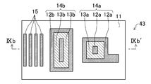
- FIG. 1A is a plan view showing an exemplary pattern 50 to be formed in the present embodiment
- FIG. 1B is a plan view showing an exemplary photomask 40 used for forming the pattern 50
- FIG. 1C is a cross-sectional view taken along the line Ic-Ic ′ in FIG.
- the transparent substrate 11 through which the exposure light is transmitted has a denseness having a line width L1 of, for example, 60 nm smaller than 0.7 ⁇ ⁇ / NA.
- Mask pattern 15 and mask patterns 14a and 14b having a line width L2 of, for example, 200 nm larger than 0.7 ⁇ ⁇ / NA are arranged.
- the dense mask pattern 15 and the mask patterns 14a and 14b have a structure in which a light shielding film 22 is laminated on a semi-light shielding film 23, as shown in FIG.
- the dense mask pattern 15 since the light shielding film 22 is laminated on the entire semi-light shielding film 23, the whole is a light shielding portion.
- the mask patterns 14a and 14b since the light shielding film 22 is laminated on a part (mainly the outer peripheral part) of the semi-light shielding film 23, the semi-light shielding parts 13a and 13b on the center side and the surrounding light shielding. It has the structure where the parts 12a and 12b were provided.
- the light-shielding portion and the semi-light-shielding portion are referred to with respect to the planar configuration as shown in FIG.
- the semi-light-shielding portions 13a and 13b transmit light in the same phase with reference to the opening (the portion of the transparent substrate 11 where no mask pattern is arranged).
- an isolated space 16 is arranged between the mask pattern 14a and the mask pattern 14b, and an isolated space 17 is arranged between the mask pattern 14b and the dense mask pattern 15.
- the isolated space 16 has the width S1
- the light shielding portions 12a and 12b have the width B1
- the semi-light shielding portion 13a and 13b has a width H1.
- FIG. 2 is a diagram showing an image of transmitted light when exposure is performed using the photomask 40.
- the light transmitted through the isolated spaces 16 and 17 and the light transmitted through the semi-shielding portions 13a and 13b have the same phase.
- the semi-light-shielding portion 13a, the light-shielding portion 12a, the isolated space 16 (opening), the light-shielding portion 12b, and the semi-light-shielding portion 13b are arranged in this order, so that the periphery of the isolated space 16
- the optical environment is bright, dark, bright, dark, bright, and has a highly periodic distribution. As a result, the DOF is improved.
- FIG. 3 shows a CD (line width dimension) change with respect to a focus variation when exposure is performed on the mask of the present embodiment including the light-shielding portion and the reflection rear portion and a normal binary mask having a pattern including only the light-shielding portion. . Both the case of normal illumination and the case of oblique incidence illumination are shown.
- the maximum width of the focus that can realize a dimensional variation of ⁇ 10 nm with respect to the target 63 nm, that is, a size within the range of 63 ⁇ 10 nm is defined as DOF.
- DOF 112 nm in combination with oblique incidence illumination
- DOF 117 nm in combination with normal illumination.
- DOF 128 nm in combination with normal illumination
- DOF 146 nm in combination with oblique incidence illumination.
- the CD change with respect to the focus fluctuation is small as compared with the case where the binary mask is used. That is, the DOF is large.
- the DOF is larger in the case of using the normal illumination than in the case of using the oblique illumination, whereas in the case of the photomask of the present embodiment, the oblique incidence illumination is used rather than using the normal illumination.
- the DOF is larger when used. This indicates that when oblique incidence illumination is used to form a fine dense pattern, it is possible to simultaneously refine the isolated space pattern (in the case of a binary mask, the fine dense pattern is reduced). If oblique incidence illumination is used to form an isolated space pattern, it becomes difficult to miniaturize the isolated space pattern because the DOF decreases.
- the light shielding portions (12a and 12b) in the photomask 40 will be further described.
- the width B1 of the light-shielding portion (see FIG. 1C) increases, the degree of light interference between the semi-light-shielding portion and the opening decreases, and the DOF related to the isolated space (16 and 17) becomes smaller than that of the binary mask. Approach the behavior. That is, it becomes difficult to obtain the effect of DOF expansion related to the isolated space. Therefore, in order to increase the DOF, it is necessary to set the width B1 of the light shielding portion to a certain value or less.
- FIG. 4 shows the relationship between the width of the light shielding part and the DOF in the isolated space.
- DOF is defined as, for example, the maximum focus width that can realize a dimensional variation within ⁇ 10 nm with respect to a target width of 63 nm.
- the width of the light-shielding portion is 0.05 ⁇ ⁇ / NA (7 nm according to the example described as the premise) or more and 1.13 ⁇ ⁇ / NA (161 nm according to the same example) or less. Then, the DOF is improved by 10 or more compared to the binary mask.
- the width of the light-shielding portion is set to 0.12 ⁇ ⁇ / NA (17 nm according to the same example) or more and 0.63 ⁇ ⁇ / NA (90 nm according to the same example) or less, 20% or more is achieved.
- the DOF can be improved.
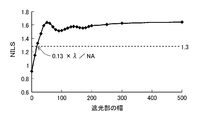
- the width B1 of the light shielding part needs to be set to a certain dimension or more from the viewpoint of NILS.
- NILS is defined as follows.
- NILS ( ⁇ lnI / ⁇ x) ⁇ W
- I is the light intensity
- ( ⁇ lnI / ⁇ x) is the logarithmic gradient of the light intensity
- W is the pattern dimension
- NILS is preferably 1.3 or more, for example.
- FIG. 5 is a diagram showing the relationship between the width B1 of the light shielding portion and NILS regarding the isolated space pattern.
- the NILS value is preferably 1.3 or more. From FIG. 5, it can be seen that the width B1 of the light shielding portion needs to be 0.13 ⁇ ⁇ / NA (18 nm in the case of the premise) or more. In addition, the width B1 of the light shielding portion necessary for obtaining a desired NILS can be obtained from FIG.
- the distance between the mask pattern having a width L2 larger than 0.7 ⁇ ⁇ / NA and the adjacent mask pattern (space dimension S1) is smaller than 0.5 ⁇ ⁇ / NA.
- the semi-light-shielding portions 13a and 13b are arranged in the mask patterns 14a and 14b having the width L2, and the light-shielding portions having a width of 0.13 ⁇ ⁇ / NA or more and 1.13 ⁇ ⁇ / NA or less around the periphery. 12a and 12b are arranged.
- sufficient NILS can be secured and the DOF of the isolated space can be improved by 10% or more.
- the width of the light shielding portion is 0.13 ⁇ ⁇ / NA or more and 0.63 ⁇ ⁇ / NA or less, sufficient NILS can be ensured and the DOF of the isolated space can be improved by 20 or more.
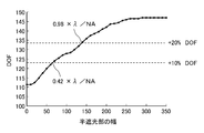
- the width of the semi-light-shielding part will be described. If the width of the semi-light-shielding portion is small, the light intensity corresponding to the semi-light-shielding portion becomes smaller than the light intensity corresponding to the isolated space pattern when exposure is performed. As a result, the periodicity of the light intensity distribution is not sufficiently increased, and the effect of DOF expansion is difficult to obtain. This will be described with reference to FIG.
- FIG. 6 shows the result of the simulation of the relationship of DOF with respect to the width of the semi-light-shielding portion. From FIG. 6, when the width of the semi-light-shielding part is larger than 0.42 ⁇ ⁇ / NA (according to the example described as the premise, it is larger than 60 nm), an example of the binary mask without the semi-light-shielding part (half It can be seen that the DOF can be enlarged by 10% compared to the case where the width of the light shielding portion is 0 nm.
- the DOF can be enlarged by 20% compared to the binary mask.
- width H1 of the semi-light-shielding portion and the width B1 of the light-shielding portion can be set to values larger than the limit of mask creation, mask creation is facilitated and cost can be reduced.
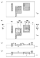
- FIGS. 7A to 7D are cross-sectional views schematically showing each step.
- a film to be processed 101 such as a metal film or an insulating film is formed on a substrate 100 made of silicon or the like.
- a positive resist film 102 is formed on the film 101 to be processed.
- the exposure light 103 is irradiated using an ArF excimer laser, a KrF excimer laser, or the like as a light source.
- the resist film 102 is exposed to the transmitted light 105 that has passed through the openings of the photomask 40 (isolated spaces 16 and 17, areas between the dense mask patterns 15 and the like), and as a result, a latent image corresponding to the openings. A portion 102a is formed.
- the latent image portion 102a is irradiated with exposure energy sufficient to completely dissolve the resist film 102 in the development process.
- the transmitted light 104 transmitted through the halftone portions (semi-shielding portions 13a and 13b) in the photomask 40 has the same phase as the transmitted light 105 transmitted through the opening, but the resist film 102 is exposed to form a latent image portion. Just don't have energy. Accordingly, only the resist film 102 corresponding to the opening of the photomask 40 is exposed.
- the mask patterns 14a and 14b having the width L2 larger than 0.7 ⁇ ⁇ / NA are spaced from the neighboring patterns by 0.5 ⁇ ⁇ / NA or less (space dimension S1).
- space dimension S1 space dimension S1
- a semi-light-shielding portion having a width larger than 0.42 ⁇ ⁇ / NA is disposed inside the pattern having the width L2, and the width thereof is larger than 0.13 ⁇ ⁇ / NA, and 1.13 ⁇ A light shielding part smaller than ⁇ / NA is arranged.
- a fine dense mask pattern 15 having a line width L1 smaller than 0.7 ⁇ ⁇ / NA is arranged with a space dimension S1 as an interval from the pattern of width L2.
- the photomask can be provided with periodicity such as bright, dark, bright, and dark in the light intensity distribution during exposure by the arrangement of the opening, the light-shielding part, and the semi-light-shielding part.
- periodicity such as bright, dark, bright, and dark in the light intensity distribution during exposure by the arrangement of the opening, the light-shielding part, and the semi-light-shielding part.
- the dimensional relationship indicated by 4-6 is realized.
- FIG. 8A is a plan view showing an exemplary pattern 51 to be formed in the present modification
- FIG. 8B is a plan view showing an exemplary photomask 41 used for forming the pattern 51
- 8C is a cross-sectional view taken along line VIIIc-VIIIc ′ in FIG. 5B
- FIG. 8D is a cross-sectional view taken along line VIIId-VIIId ′ in FIG. 5B.
- FIGS. 8A to 8D the same components as those in FIGS. 1A to 1C are denoted by the same reference numerals.
- the photomask 41 also includes semi-light-shielding portions 13a and 13b inside the mask patterns 14a and 14b, and the light-shielding portions 12a and 12b are arranged around it. Further, the mask patterns 14a and 14b having the width L2 are arranged with a space dimension S1 in the Vc-Vc ′ line direction (in a direction in which the mask patterns face each other with an isolated space therebetween).
- the mask pattern 14a is not arranged side by side with the mask pattern 14b, and a space dimension S2 larger than 0.5 ⁇ ⁇ / NA ⁇ M is provided.
- the mask pattern 15a is arranged side by side.
- a predetermined value a value determined by ⁇ , NA, M, for example, 0.5 ⁇ ⁇ / NA ⁇ M. In such a portion, the semi-light-shielding portion 13a is not disposed.
- the semi-light-shielding portion 13b is arranged in a portion aligned with the mask pattern 14a and the space dimension S1.
- the semi-light-shielding portion is disposed in the mask pattern, and the portion disposed with the space dimension S2 having a size that does not require DOF expansion is semi-light-shielded.
- the part is not arranged.
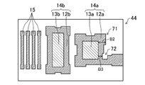
- FIG. 9A is a plan view showing another exemplary photomask 42, and the photomask 42 has a pattern for forming the pattern of FIG. 1A.
- FIG. 9B is a diagram showing a cross section taken along line IXb-IXb ′ in FIG.
- the light shielding portions 12a and 12b are arranged on the peripheral portions of the mask patterns 14a and 14b, and the semi-light shielding portions 13a and 13b are formed as a continuous region.
- the light shielding portions 12a and 12b are also formed inside the mask patterns 14a and 14b, and the semi-light shielding portions 13a and 13b are divided into a plurality of portions.
- the periodicity of light, dark, bright, and dark in the light intensity distribution can be further enhanced as shown in FIG. 10, so that the DOF of the isolated space is further expanded. be able to.
- FIG. 11 shows still another exemplary photomask 43 for forming the pattern of FIG.
- the light shielding portions 12a and 12b are arranged in an independent island shape inside the semi-light shielding portions 13a and 13b in addition to the peripheral portions of the mask patterns 14a and 14b.
- the cross section taken along line IXb-IXb ′ in FIG. 11 is the same as FIG. 9B. Therefore, the light and darkness in the light intensity distribution when exposed using the photomask 43 has high periodicity, and the DOF expansion can be realized.
- the semi-light-shielding portions and the light-shielding portions are arranged alternately.
- a protruding portion that does not reach the light shielding portion on the opposite side may be provided from a part of the light shielding portion that surrounds the semi-light shielding portion.
- FIG. 12 shows still another exemplary photomask 44 for forming the pattern of FIG.
- the photomask 44 is the same as the photomask 40 in FIG. 1B in that the semi-light-shielding portions 13a and 13b are arranged at the peripheral portions of the mask patterns 14a and 14b.
- the width B2 of the planar convex corner portion 71 is larger than the width B3 of the concave corner portion 72.
- OPC optical proximity effect correction
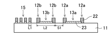
- FIGS. 13 and 14 are schematic cross-sectional views illustrating other configurations for providing the semi-light-shielding portion and the light-shielding portion.
- the semi-light-shielding portions 23a and 13b are formed by forming the semi-light-shielding film 23 on the transparent substrate 11 and providing the light-shielding film 22 at necessary locations on the semi-light-shielding film 23.
- the light shielding portions 12a and 12b are configured.
- the light shielding film 22 is formed at a necessary location on the transparent substrate 11, and the semi-light shielding film 23 is formed at the necessary location on the transparent substrate 11 so as to cover the light shielding film 22.
- semi-light-shielding portions 13a and 13b and light-shielding portions 12a and 12b are configured.
- the semi-light-shielding film 23 is patterned at a necessary portion on the transparent substrate 11, and the light-shielding film 22 is formed on the semi-light-shielding film 23 and the necessary portions on the transparent substrate 11, thereby forming a semi-light-shielding portion. 13a and 13b and light shielding parts 12a and 12b are configured.
- the side surfaces of the semi-light-shielding film 23 and the light-shielding film 22 are flush, whereas in the case of FIG. 14, the light-shielding film 22 is formed so as to cover the side surface of the semi-light-shielding film 23. A portion in contact with the transparent substrate 11 is provided.
- the width of the light shielding portion is from the edge on the space pattern side to the edge on the opposite side in the light shielding portion.
- the width of the light shielding portion is set to a predetermined value (for example, a value larger than 0.13 ⁇ ⁇ / NA and smaller than 1.13 ⁇ ⁇ / NA), so that the isolation is achieved.
- a predetermined value for example, a value larger than 0.13 ⁇ ⁇ / NA and smaller than 1.13 ⁇ ⁇ / NA
- the photomask of the present disclosure and the pattern forming method using the photomask, it is possible to simultaneously form a dense pattern and an isolated space pattern without generating side lobes, and to easily create a photomask. Therefore, it is also useful in pattern formation in a process in which an SRAM portion (dense pattern) and a logic portion (isolated space pattern) such as element isolation exist simultaneously.
Abstract
A photomask (40) comprises a transparent substrate (11) and a first mask pattern (14b) and a second mask pattern (14a, 15) which are arranged on the transparent substrate (11) and respectively have parts that face each other through a space (16, 17). The first mask pattern (14b) comprises a light half-shielding part (13b) through which light can transmit partially and a light shielding part (12b). In the first mask pattern (14b), the light half-shielding part (13b) is so adapted as to have a part that faces the space (16, 17) through the light shielding part (12b). The size of the first mask pattern (14b) is larger than (0.7×λ/NA)×M, and the size of the space (16, 17) is (0.5×λ/NA)×M or smaller (wherein λ represents the wavelength of exposure light; NA represents the number of openings in a reducing projection optical system of an exposure machine; and M represents the magnification of the reducing projection optical system).
Description
本開示は、半導体集積回路装置の製造に用いられる微細パターン形成用のフォトマスクと、そのフォトマスクを用いたパターン形成方法に関する。
The present disclosure relates to a photomask for forming a fine pattern used for manufacturing a semiconductor integrated circuit device, and a pattern forming method using the photomask.
近年、半導体を用いて実現する大規模集積回路装置(以下LSIと称する)の高集積化を実現するために、回路パターンの微細化がますます必要となっている。その中でも素子分離に関して、LSIには、SRAM(Static Random Access Memory )等に代表される微細な密集パターンと、スタンダードセル等で多く見られる微細な孤立スペースパターンとが同時に存在する。LSIの高集積化のためには、これら2種類のパターンを同時に微細化することが重要になっている。
In recent years, in order to achieve high integration of large scale integrated circuit devices (hereinafter referred to as LSIs) realized using semiconductors, circuit patterns have become increasingly finer. Among them, with regard to element isolation, LSI has a fine dense pattern typified by SRAM (Static Random Access Memory) and the like, and a fine isolated space pattern often found in standard cells. In order to achieve high integration of LSI, it is important to make these two types of patterns finer simultaneously.
微細な密集パターンの形成には、超解像露光と呼ばれる斜入射露光を用いることが行なわれている。この方法は、より微細な密集パターンを形成するために有利であると共に、周期的に配置された密集パターンのDOF(Depth Of Focus、焦点深度)を向上させる効果も有する。しかしながら、斜入射露光方法は、孤立スペースパターンに対しては解像度向上の効果が無く、逆に、DOFを大きく劣化させてしまう。
For forming a fine dense pattern, oblique incidence exposure called super-resolution exposure is used. This method is advantageous for forming a finer dense pattern and also has an effect of improving the DOF (Depth Of Focus) of the densely arranged dense pattern. However, the oblique incidence exposure method has no effect of improving the resolution with respect to the isolated space pattern, and conversely, the DOF is greatly deteriorated.
この一方、微細な孤立スペースパターンを形成するために干渉度の小さい光源を用いると、微細な密集パターンの形成が困難になる。
On the other hand, if a light source with a small interference degree is used to form a fine isolated space pattern, it becomes difficult to form a fine dense pattern.
以上のように、微細な孤立スペースパターンと微細な密集パターンとに対する最適照明条件は、相反関係にある。従って、微細な密集パターンの形成と微細な孤立スペースパターンの形成とを同時に行なうために、光源からの垂直入射成分及び斜入射成分のいずれも存在するように、干渉度が0.5~0.6程度の光源を用いている。
As described above, the optimum illumination conditions for a fine isolated space pattern and a fine dense pattern are in a reciprocal relationship. Therefore, in order to perform the formation of a fine dense pattern and the formation of a fine isolated space pattern at the same time, the interference degree is 0.5 to 0.00 so that both the normal incidence component and the oblique incidence component from the light source exist. About 6 light sources are used.
しかしこの場合、垂直入射成分と斜入射成分の両方が相殺されるので、密集パターンと孤立スペースパターンとを同時に微細化して更なる半導体装置の微細化を実現することは困難である。
However, in this case, since both the normal incidence component and the oblique incidence component are canceled out, it is difficult to realize further miniaturization of the semiconductor device by simultaneously miniaturizing the dense pattern and the isolated space pattern.
これに対しては、例えば特許文献1に記載されているように、補助パターンを用いることが有効である。
For this, it is effective to use an auxiliary pattern as described in Patent Document 1, for example.
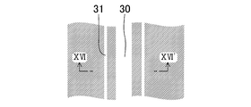
微細な密集パターンを形成するために斜入射照明を用いた場合、孤立スペースパターンの部分ではDOFの大幅な低下が起る。これに対し、図15に示すように補助パターン31をメインパターン30の近傍に配置すると、孤立スペースパターンの部分におけるDOFを拡大することができる。
When oblique incidence illumination is used to form a fine dense pattern, a significant reduction in DOF occurs in the isolated space pattern portion. On the other hand, when the auxiliary pattern 31 is arranged in the vicinity of the main pattern 30 as shown in FIG. 15, the DOF in the isolated space pattern portion can be enlarged.
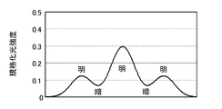
図16には、図15に例示したパターンに対して斜入射照明を用いた場合について、図15のXVI-XVI'線における光強度を表すグラフである。光透過部からなるメインパターン30(孤立スペースパターンに対応する)の近くに、解像不能な寸法の光透過部からなる補助パターン31を配置して露光を行なう。これにより、図16に示すように、光強度が明、暗、明、暗、明と周期性を持つようになり、結果として孤立スペースパターンの部分におけるDOFが向上する。
FIG. 16 is a graph showing the light intensity at the XVI-XVI ′ line in FIG. 15 when oblique incidence illumination is used for the pattern illustrated in FIG. Exposure is performed by placing an auxiliary pattern 31 made of a light transmissive portion having a size that cannot be resolved near the main pattern 30 made of the light transmissive portion (corresponding to the isolated space pattern). As a result, as shown in FIG. 16, the light intensity has periodicity such as bright, dark, bright, dark, and bright, and as a result, the DOF in the isolated space pattern portion is improved.
このとき、補助パターン31について、ウェハ上に転写されるのを避ける必要がある。このために、補助パターン31の幅を、メインパターン30よりも小さい、解像限界以下の寸法に設定する。また、一般的に補助パターンはメインパターンに対してルールベース配置される。補助パターンの配置後に、メインパターンに対してモデルベースOPC(Optical Proximity Correction)を行なうのが通常である。
At this time, it is necessary to avoid transferring the auxiliary pattern 31 onto the wafer. For this purpose, the width of the auxiliary pattern 31 is set to a dimension smaller than the main pattern 30 and less than the resolution limit. In general, the auxiliary pattern is arranged in a rule base with respect to the main pattern. After the auxiliary pattern is arranged, model-based OPC (Optical / Proximity / Correction) is usually performed on the main pattern.
前述のように、補助パターンは解像限界以下の寸法であることが必要である。しかしながら、回路パターンの微細化に伴い、大きなDOF拡大の効果を得るために必要な補助パターンの大きさは、解像限界に近い寸法になっている。更に、補助パターンは、スタンダードセルのようなランダムなパターンに対してルールベースにより配置される。
As described above, the auxiliary pattern needs to have a dimension less than the resolution limit. However, with the miniaturization of circuit patterns, the size of the auxiliary pattern necessary for obtaining a large DOF enlargement effect is close to the resolution limit. Further, the auxiliary pattern is arranged on a rule basis with respect to a random pattern such as a standard cell.
これらのことから、周辺のメインパターンの環境次第では、補助パターンに対応する光強度が、転写の生じる光強度の閾値を越えてしまうことがある。この場合、サイドローブと呼ばれる不要なパターンがウェハ上に形成される。
For these reasons, depending on the environment of the surrounding main pattern, the light intensity corresponding to the auxiliary pattern may exceed the threshold value of the light intensity at which transfer occurs. In this case, an unnecessary pattern called a side lobe is formed on the wafer.
また、補助パターンは、メインパターンよりも小さい寸法であることが必要である。しかしながら、メインパターン自体が微細化されてマスク作成限界に近付くに従い、メインパターンよりも小さく設計される補助パターンを有するマスクの製造は困難になる。
Also, the auxiliary pattern needs to be smaller than the main pattern. However, as the main pattern itself is miniaturized and approaches the mask production limit, it becomes difficult to manufacture a mask having an auxiliary pattern designed to be smaller than the main pattern.
また、フォトマスクにおける補助パターンの寸法変動は、転写されるメインパターンの寸法に大きく影響するので、補助パターンのマスクは高い寸法精度に作成する必要がある。しかし、補助パターンはマスク作成限界の近くまで小さくなっているので、高い寸法精度にマスクを作成することは難しく、不可能にもなり得る。更に、マスクの検査等も困難になり、マスクの作成時間の長期化、マスクの製造コストの上昇を起こす可能性がある。
Also, since the dimension variation of the auxiliary pattern in the photomask greatly affects the dimension of the main pattern to be transferred, it is necessary to create the mask of the auxiliary pattern with high dimensional accuracy. However, since the auxiliary pattern is reduced to near the mask production limit, it is difficult and impossible to produce a mask with high dimensional accuracy. Furthermore, mask inspection or the like becomes difficult, and there is a possibility of prolonging the mask preparation time and increasing the mask manufacturing cost.
以上に鑑み、本開示の技術は(特に、微細な密集パターンを形成するために斜入射照明を用いる場合の孤立スペースパターンについて)DOFを向上することができ且つ転写後のパターンにサイドローブを発生させることのないフォトマスク及びそれを用いたパターン形成方法を実現することを目的とする。
In view of the above, the technology of the present disclosure can improve the DOF (particularly for an isolated space pattern when oblique incidence illumination is used to form a fine dense pattern) and generate side lobes in the transferred pattern. An object of the present invention is to realize a photomask and a pattern forming method using the same.
本願発明者等は、前記のような光透過部からなる補助パターンを用いることなくDOFを向上させると共にサイドローブの発生を抑える方法を種々検討した。その結果、フォトマスクを用いた露光に際し、光強度分布に明、暗、明、暗のような周期性を持たせるために、露光光を部分的に透過させる半遮光部を利用することに想到した。
The inventors of the present application have studied various methods for improving the DOF and suppressing the occurrence of side lobes without using the auxiliary pattern composed of the light transmitting portion as described above. As a result, upon exposure using a photomask, the idea is to use a semi-shielding portion that partially transmits exposure light in order to give the light intensity distribution periodicity such as bright, dark, bright, and dark. did.
具体的に、本開示の第1のフォトマスクは、透明基板と、透明基板上に、スペースを挟んで対向する部分を有するように形成された第1マスクパターン及び第2マスクパターンを備え、第1マスクパターンは、光を部分的に透過させる半遮光部と、遮光部とを含み、第1マスクパターンにおいて、半遮光部は、遮光部を挟んでスペースと対向する部分を有するように配置され、第1マスクパターンと第2マスクパターンとの対向方向について、第1マスクパターンの寸法は、(0.7×λ/NA)×Mよりも大きく、スペースの寸法は、(0.5×λ/NA)×M以下である(但し、λは露光光の波長であり、NAは露光機の縮小投影光学系の開口数であり、Mは縮小投影光学系の倍率である)。
Specifically, a first photomask of the present disclosure includes a transparent substrate, and a first mask pattern and a second mask pattern formed on the transparent substrate so as to have portions facing each other with a space interposed therebetween, One mask pattern includes a semi-light-shielding part that partially transmits light and a light-shielding part. In the first mask pattern, the semi-light-shielding part is arranged to have a portion that faces the space with the light shielding part interposed therebetween. In the opposing direction of the first mask pattern and the second mask pattern, the dimension of the first mask pattern is larger than (0.7 × λ / NA) × M, and the dimension of the space is (0.5 × λ / NA) × M or less (where λ is the wavelength of the exposure light, NA is the numerical aperture of the reduction projection optical system of the exposure machine, and M is the magnification of the reduction projection optical system).
このようなフォトマスクによると、第1マスクパターンと第2マスクパターンとの対向方向について、第1マスクパターンの半遮光部、第1マスクパターンの遮光部、スペース、第2マスクパターン、と並んでいる。従って、露光時にこれらの部分に対応する光強度分布において、明、暗、明、暗、のような周期性を持たせることができ、DOFを向上させることができる。特に、微細な密集パターンを形成するために斜入射照明を用いると、半遮光部を備えないバイナリマスクの場合とは異なり、スペースのDOFについても大きくなるので、いずれのパターンについてもより適正に形成することができる。
According to such a photomask, the opposing direction of the first mask pattern and the second mask pattern is aligned with the semi-light-shielding portion of the first mask pattern, the light-shielding portion of the first mask pattern, the space, and the second mask pattern. Yes. Accordingly, the light intensity distribution corresponding to these portions at the time of exposure can have periodicity such as bright, dark, bright, dark, and the DOF can be improved. In particular, when oblique incidence illumination is used to form a fine dense pattern, the space DOF is increased, unlike the case of a binary mask that does not include a semi-light-shielding portion, so that any pattern can be formed more appropriately. can do.
ここで、半遮光部の光透過率は、フォトマスクを用いて露光を行なう際に、半遮光部を透過した光がレジスト等を感光しない(感光領域を発生させない)光強度となるように設定することができる。これにより、DOF向上のために設けた半遮光部が、不要なパターン(サイドローブ)を発生させるのを避けることができる。これと共に、第1マスクパターンにおける半遮光部及び遮光部の寸法について、マスクの加工限界よりも大きい寸法にすることができる。つまり、フォトマスクの作成がより容易になる。
Here, the light transmittance of the semi-light-shielding part is set so that the light transmitted through the semi-light-shielding part has a light intensity that does not sensitize the resist or the like (does not generate a photosensitive area) when performing exposure using a photomask. can do. Thereby, it is possible to prevent the semi-light-shielding portion provided for improving the DOF from generating an unnecessary pattern (side lobe). At the same time, the dimensions of the semi-light-shielding part and the light-shielding part in the first mask pattern can be made larger than the processing limit of the mask. That is, it becomes easier to create a photomask.
尚、第2マスクパターンは遮光部からなり、第1マスクパターンと第2マスクパターンとの対向方向について、第2マスクパターンの寸法は、(0.7×λ/NA)×M以下であっても良い。
The second mask pattern includes a light-shielding portion, and the dimension of the second mask pattern is (0.7 × λ / NA) × M or less in the opposing direction of the first mask pattern and the second mask pattern. Also good.
スペースを介して第1マスクパターンと対向する部分の第2マスクパターンの寸法が小さい場合には、第2マスクパターンを遮光部からなるものにすると共に、以上の寸法に設定する。これにより、いずれのパターンについてもDOFを向上させることができる。
When the dimension of the second mask pattern at the portion facing the first mask pattern through the space is small, the second mask pattern is made of a light shielding portion and set to the above dimensions. Thereby, DOF can be improved about any pattern.
また、半遮光部及び遮光部は、第2マスクパターンにも他の半遮光部及び他の遮光部として含まれており、第2マスクパターンにおいて、他の半遮光部は、他の遮光部を挟んでスペースと対向するように配置されていても良い。
The semi-light-shielding portion and the light-shielding portion are also included in the second mask pattern as other semi-light-shielding portions and other light-shielding portions. In the second mask pattern, the other semi-light-shielding portions are replaced with other light-shielding portions. You may arrange | position so that it may oppose and space on both sides.
このようにすると、第1マスクパターンの半遮光部、第1マスクパターンの遮光部、スペース、第2マスクパターンの遮光部、第2マスクパターンの半遮光部、と並ぶので、露光時の光強度分布において、明、暗、明、暗、明、との周期性が実現する。これにより、DOFが向上する。
In this case, the light intensity at the time of exposure is aligned with the semi-light-shielding portion of the first mask pattern, the light-shielding portion of the first mask pattern, the space, the light-shielding portion of the second mask pattern, and the semi-light-shielding portion of the second mask pattern. In the distribution, periodicity of light, dark, light, dark, and light is realized. Thereby, DOF improves.
また、第1マスクパターンと第2マスクパターンとの対向方向について、第2マスクパターンの寸法は、(0.7×λ/NA)×Mよりも大きくても良い。
Also, the dimension of the second mask pattern may be larger than (0.7 × λ / NA) × M in the opposing direction of the first mask pattern and the second mask pattern.
スペースを介して第1マスクパターンと対向する部分の第2マスクパターンの寸法が大きい場合には、第2マスクパターンを遮光部及び半遮光部が含まれるものにすると共に、以上の寸法に設定する。これにより、いずれのパターンについてもDOFを向上させることができる。
When the dimension of the second mask pattern in the portion facing the first mask pattern through the space is large, the second mask pattern includes the light shielding part and the semi-light shielding part and is set to the above dimension. . Thereby, DOF can be improved about any pattern.
また、第1マスクパターンと第2マスクパターンとの対向方向について、遮光部の寸法及び半遮光部の寸法は、λ、NA及びMに基づいて設定されていても良い(但し、λは露光光の波長であり、NAは露光機の縮小投影光学系の開口数であり、Mは縮小投影光学系の倍率である)。
Further, with respect to the opposing direction of the first mask pattern and the second mask pattern, the dimension of the light shielding part and the dimension of the semi-light shielding part may be set based on λ, NA and M (where λ is the exposure light) NA is the numerical aperture of the reduction projection optical system of the exposure machine, and M is the magnification of the reduction projection optical system).
遮光部及び半遮光部の寸法を決める要素の例としては、以上のものが挙げられる。
The above are mentioned as an example of the element which determines the dimension of a light-shielding part and a semi-light-shielding part.
また、遮光部の寸法は、(0.13×λ/NA)×M以上であっても良い。
Further, the dimension of the light shielding portion may be (0.13 × λ / NA) × M or more.
このような値とすると、フォトマスクを用いて露光する際に、十分な露光量余裕度を得ることができる。
With such a value, a sufficient exposure amount margin can be obtained when exposure is performed using a photomask.
また、遮光部の寸法は、(1.13×λ/NA)×M以下であっても良い。
Also, the dimension of the light shielding part may be (1.13 × λ / NA) × M or less.
このような値とすると、DOFを顕著に向上することができる。
When such values are used, the DOF can be remarkably improved.
また、半遮光部の寸法は、(0.42×λ/NA)×M以上であっても良い。
Further, the dimension of the semi-light-shielding portion may be (0.42 × λ / NA) × M or more.
このような値とすると、DOFを顕著に向上することができる。
When such values are used, the DOF can be remarkably improved.
また、半遮光部は、スペースと同位相で光を透過させても良い。
Also, the semi-shielding part may transmit light with the same phase as the space.
このようにすると、より適正にパターンを露光することができる。
In this way, the pattern can be exposed more appropriately.
また、遮光部は、半遮光部を囲むように配置されていても良い。
Further, the light shielding part may be arranged so as to surround the semi-light shielding part.
このようにすると、マスクパターンに関していずれの方向についても、露光時の光強度分布について明、暗、明、の周期性を実現することができる。
In this way, it is possible to realize light, dark, and light periodicity of the light intensity distribution during exposure in any direction with respect to the mask pattern.
また、遮光部の幅は、半遮光部の凹コーナー部よりも半遮光部の凸コーナー部において広くても良い。
Further, the width of the light shielding part may be wider at the convex corner part of the semi-light-shielding part than the concave corner part of the semi-light-shielding part.
このようにすると、光近接効果補正により、特にコーナー部の形状に関して、所望の露光パターンをより確実に得ることができる。
In this way, the desired exposure pattern can be obtained more reliably by the optical proximity effect correction, particularly with respect to the shape of the corner portion.
また、半遮光部は、遮光部によって複数の部分に分割されていても良い。
Moreover, the semi-light-shielding part may be divided into a plurality of parts by the light-shielding part.
また、遮光部は、前記対向方向について半遮光部に挟まれた部分を有していても良い。
Further, the light shielding part may have a portion sandwiched between the semi-light shielding parts in the facing direction.
このようにすると、遮光部と半遮光部とによって、露光時の光強度分布について明、暗、明の周期性を更に高めることができる。
In this way, the light, light, and light shading parts can further improve the light, dark, and light periodicity of the light intensity distribution during exposure.
また、半遮光部の光透過率は、半遮光部を透過した光が、感光領域を発生させる光強度よりも弱い光強度となるように設定されていても良い。
Further, the light transmittance of the semi-light-shielding part may be set so that the light transmitted through the semi-light-shielding part has a light intensity that is weaker than the light intensity that generates the photosensitive region.
このようにすると、露光時に、半遮光部を透過した光によって不要なパターンが生じるのを避けることができる。
In this way, it is possible to avoid generation of an unnecessary pattern due to the light transmitted through the semi-shielding portion during exposure.
また、半遮光部は、遮光部を挟んでスペースと対向する部分のみに配置されていても良い。
Moreover, the semi-light-shielding part may be arranged only in a part facing the space with the light-shielding part interposed therebetween.
このようにすると、必要な箇所のDOFを拡大することができるとことに加えて、フォトマスクの加工が容易になると共に描画時間の短縮が可能になり、マスクコストの削減が実現する。
In this way, in addition to being able to enlarge the DOF at a necessary location, the photomask can be easily processed and the drawing time can be shortened, thereby reducing the mask cost.
次に、本開示の第2のフォトマスクは、反射基板と、反射基板上に、スペースを挟んで対向する部分を有するように形成された第1マスクパターン及び第2マスクパターンとを備え、第1マスクパターンは、光を部分的に反射させる半反射部と、光を実質的に反射しない非反射部とを含み、第1マスクパターンにおいて、半反射部は、非反射部を挟んでスペースと対向するように配置され、第1マスクパターンと第2マスクパターンとの対向方向について、第1マスクパターンの寸法は、(0.7×λ/NA)×Mよりも大きく、スペースの寸法は、(0.5×λ/NA)×M以下である(但し、λは露光光の波長であり、NAは露光機の縮小投影光学系の開口数であり、Mは縮小投影光学系の倍率である)。
Next, a second photomask of the present disclosure includes a reflective substrate, and a first mask pattern and a second mask pattern formed on the reflective substrate so as to have portions facing each other with a space interposed therebetween, One mask pattern includes a semi-reflective part that partially reflects light and a non-reflective part that does not substantially reflect light. In the first mask pattern, the semi-reflective part includes a space with the non-reflective part interposed therebetween. The dimensions of the first mask pattern are larger than (0.7 × λ / NA) × M in the facing direction of the first mask pattern and the second mask pattern. (0.5 × λ / NA) × M or less (where λ is the wavelength of exposure light, NA is the numerical aperture of the reduction projection optical system of the exposure machine, and M is the magnification of the reduction projection optical system) is there).
これは、本開示の第1のフォトマスクが透過型のフォトマスクであるのに対し、同様の効果を有するように反射型のフォトマスクとして実現したものである。第1のフォトマスクに関する以上の説明において、透明基板を反射基板、半遮光部を半反射部、遮光部を非反射部、透過を反射、光透過率を光反射率、等のように読み替えることにより、第2のフォトマスクに関する説明となる。
This is realized as a reflection type photomask so as to have the same effect as the first photomask of the present disclosure is a transmission type photomask. In the above description regarding the first photomask, the transparent substrate is read as a reflective substrate, the semi-light-shielding part as a semi-reflective part, the light-shielding part as a non-reflective part, the transmission as reflected, and the light transmittance as light reflectance. Thus, the second photomask is described.
次に、本開示のパターン形成方法は、本開示のいずれか1つのフォトマスクを用い、基板上にレジスト膜を形成する工程(a)と、レジスト膜に、フォトマスクを介して露光光を照射する工程(b)と、露光光が照射されたレジスト膜を現像し、レジスト膜をパターン化する工程(c)とを備える。
Next, the pattern forming method of the present disclosure uses any one photomask of the present disclosure to form a resist film on the substrate (a) and irradiate the resist film with exposure light through the photomask. And a step (c) of developing a resist film irradiated with exposure light and patterning the resist film.
このようなパターン形成方法によると露光時に、不要なパターンの発生を抑制しながら、DOFを向上することができる。この結果、特に、微細な密集パターンを形成するために斜入射照明を用いる場合に、孤立スペースパターンについてDOFが大きくなるので、いずれのパターンについてもより適正に形成することができる。
According to such a pattern formation method, DOF can be improved while suppressing generation of unnecessary patterns during exposure. As a result, particularly when oblique incidence illumination is used to form a fine dense pattern, the DOF increases for the isolated space pattern, so that any pattern can be formed more appropriately.
尚、工程(b)において、斜入射照明を用いても良い。
In the step (b), oblique incidence illumination may be used.
このようにすると、更に適正にパターンを形成することができる。
In this way, a pattern can be formed more appropriately.
以上の通り、本開示のフォトマスク及びこれを用いたパターン形成方法によると、パターンを精度良く且つサイドローブの発生無く形成することができ、且つ、フォトマスクの作成についても容易になる。特に、斜入射照明を用いて微細な密集パターンと孤立スペースパターンを共に形成する際に顕著な効果を発揮し、微細な半導体装置を製造することができる。
As described above, according to the photomask of the present disclosure and the pattern forming method using the photomask, it is possible to form a pattern with high accuracy and without generation of side lobes, and to easily create a photomask. In particular, when a fine dense pattern and an isolated space pattern are formed together using oblique incidence illumination, a remarkable effect can be exhibited and a fine semiconductor device can be manufactured.
(前提事項)
まず、本開示の実施形態を説明するに当たっての前提事項について説明する。 (Prerequisite)
First, the premise for describing the embodiment of the present disclosure will be described.
まず、本開示の実施形態を説明するに当たっての前提事項について説明する。 (Prerequisite)
First, the premise for describing the embodiment of the present disclosure will be described.
通常、フォトマスクは縮小投影型の露光機において使用されるので、マスク上のパターン寸法を議論する場合には、縮小倍率を考慮しなければならない。しかし、以下の実施形態では、混乱を避けるために、形成しようとする所望のパターン(例えばレジストパターン)と対応させてマスク上のパターン寸法を説明する場合、特に断らない限りは縮小倍率によって該寸法を換算した値を用いている。具体例を示すと、M分の1縮小投影システムにおいて、幅M×63nmのマスクパターンによって幅63nmのレジストパターンを形成した場合について、マスクパターン幅及びレジストパターン幅は共に63nmであると表現する。
Usually, since a photomask is used in a reduction projection type exposure machine, the reduction magnification must be considered when discussing the pattern dimensions on the mask. However, in the following embodiments, in order to avoid confusion, when the pattern dimensions on the mask are described in correspondence with a desired pattern to be formed (for example, a resist pattern), the dimensions are reduced by a reduction ratio unless otherwise specified. The converted value is used. As a specific example, when a resist pattern having a width of 63 nm is formed by a mask pattern having a width of M × 63 nm in a 1 / M reduction projection system, both the mask pattern width and the resist pattern width are expressed as 63 nm.
また、本開示の実施形態において、特に断らない限り、M及びNAは露光機の縮小投影光学系の縮小倍率及び開口数をそれぞれ表し、λは露光光の波長を表すものとする。フォトマスク上に形成されるマスクパターンは、レジスト膜等に対して転写する際のパターン寸法制御性の観点から、用いる露光装置の光学条件(M、NA、λ)を予め決めた上で作成される。従って、予め決められた光学条件と異なる光学条件の露光装置で用いることは一般的には行なわない。
In the embodiment of the present disclosure, unless otherwise specified, M and NA represent the reduction magnification and numerical aperture of the reduction projection optical system of the exposure machine, respectively, and λ represents the wavelength of the exposure light. The mask pattern formed on the photomask is created with predetermined optical conditions (M, NA, λ) of the exposure apparatus used from the viewpoint of pattern dimension controllability when transferring to a resist film or the like. The Therefore, it is generally not used in an exposure apparatus having an optical condition different from a predetermined optical condition.
また、パターン形成について、レジストの非感光領域がレジストパターンとなるポジ型レジストプロセスを想定して説明する。尚、ポジ型レジストプロセスに代えてネガ型レジストプロセスを用いる場合、ネガ型レジストプロセスにおいては、レジストの非感光領域が除去されるので、ポジ型レジストプロセスにおけるレジストパターンをスペースパターンと読み替えればよい。
The pattern formation will be described assuming a positive resist process in which the non-photosensitive region of the resist becomes a resist pattern. In the case of using a negative resist process instead of the positive resist process, the non-photosensitive region of the resist is removed in the negative resist process, so the resist pattern in the positive resist process may be read as a space pattern. .
また、フォトマスクとしては透過型マスクを前提として説明する。尚、透過型マスクに代えて反射型マスクを前提とする場合、反射型マスクにおいては、透過型マスクの透過領域及び遮光領域がそれぞれ反射領域及び非反射領域となるので、透過型マスクの透過現象を反射現象と読み替えればよい。具体的には、透過型マスクの開口部又は透過性領域を反射部又は反射領域と読み替え、遮光部を非反射部と読み替えればよい。さらに、透過型マスクにおける光を部分的に透過する領域(半遮光部)は光を部分的に反射する領域(半反射部)と読み替えればよく、透過率は反射率と読み替えればよい。
Also, the description will be made on the assumption that the photomask is a transmissive mask. In the case of assuming a reflective mask instead of the transmissive mask, in the reflective mask, the transmissive area and the light-shielded area of the transmissive mask become a reflective area and a non-reflective area, respectively. Can be read as a reflection phenomenon. Specifically, an opening or a transmissive region of the transmissive mask may be read as a reflective portion or a reflective region, and a light shielding portion may be read as a non-reflective portion. Furthermore, a region that partially transmits light (semi-shielding portion) in the transmission mask may be read as a region that partially reflects light (semi-reflecting portion), and the transmittance may be read as reflectance.
更に、実施形態において、各種の条件の一例として、以下のような場合を考える。
Furthermore, in the embodiment, the following cases are considered as examples of various conditions.
半遮光部は、露光光に対して例えば9%の透過率を有すると共に、その透過光は、透過部における透過光と同位相となるものと設定する。また、遮光部の露光光に対する透過率は0%である、つまり、遮光部は露光光を完全に遮光するものと設定する。
The semi-light-shielding portion is set to have a transmittance of, for example, 9% with respect to the exposure light, and the transmitted light is in phase with the transmitted light in the transmissive portion. Further, the transmittance of the light shielding portion with respect to the exposure light is 0%, that is, the light shielding portion is set to completely shield the exposure light.
また、露光は、ArF光源の波長193nm光を用い、NAは1.35とする。更に、斜入射照明としてσ_out=0.85、σ_in=0.57のAnnular 照明を用いる。
In addition, for the exposure, light with a wavelength of 193 nm from an ArF light source is used and NA is 1.35. Furthermore, as the oblique incidence illumination, Annular illumination with σ_out = 0.85 and σ_in = 0.57 is used.
また、密集パターンは、例えばピッチ120nm以下のLine/Spaceが3個以上集合したパターンとし、孤立スペースは、スペース幅に対して、少なくとも片側のライン幅が各々スペース幅の3倍以上あるパターンを考えるものとした。
The dense pattern is, for example, a pattern in which three or more lines / spaces with a pitch of 120 nm or less are gathered, and the isolated space is a pattern in which at least one line width is at least three times the space width with respect to the space width. It was supposed to be.
但し、以上は例示であって、これらに限定されるものではない。
However, the above is an example, and the present invention is not limited to these.
(実施形態)
以下、本開示の一実施形態について、図面を参照しながら説明する。 (Embodiment)
Hereinafter, an embodiment of the present disclosure will be described with reference to the drawings.
以下、本開示の一実施形態について、図面を参照しながら説明する。 (Embodiment)
Hereinafter, an embodiment of the present disclosure will be described with reference to the drawings.
図1(a)は、本実施形態において形成しようとしている例示的パターン50を示す平面図であり、図1(b)は、パターン50の形成に用いる例示的フォトマスク40を示す平面図であり、図1(c)は、図1(b)におけるIc-Ic'線における断面図である。
FIG. 1A is a plan view showing an exemplary pattern 50 to be formed in the present embodiment, and FIG. 1B is a plan view showing an exemplary photomask 40 used for forming the pattern 50. FIG. 1C is a cross-sectional view taken along the line Ic-Ic ′ in FIG.
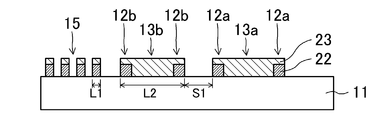
図1(b)及び(c)に示すように、フォトマスク40において、露光光を透過させる透明基板11に、それぞれが0.7×λ/NAよりも小さい例えば60nmのライン幅L1を有する密集マスクパターン15と、0.7×λ/NAよりも大きい例えば200nmのライン幅L2を有するマスクパターン14a及び14bが配置されている。
As shown in FIGS. 1B and 1C, in the photomask 40, the transparent substrate 11 through which the exposure light is transmitted has a denseness having a line width L1 of, for example, 60 nm smaller than 0.7 × λ / NA. Mask pattern 15 and mask patterns 14a and 14b having a line width L2 of, for example, 200 nm larger than 0.7 × λ / NA are arranged.
密集マスクパターン15及びマスクパターン14a及び14bは、図1(c)に示すように、半遮光膜23上に遮光膜22が積層された構造を有する。密集マスクパターン15については、半遮光膜23の全体に遮光膜22が積層されているので、全体が遮光部となっている。これに対し、マスクパターン14a及び14bについては、半遮光膜23の一部分(主に外周部分)に遮光膜22が積層されているので、中央側の半遮光部13a及び13bと、その周囲の遮光部12a及び12bとが設けられた構造となっている。このように、遮光部・半遮光部とは、図1(b)のような平面構成に関して言うものとする。
The dense mask pattern 15 and the mask patterns 14a and 14b have a structure in which a light shielding film 22 is laminated on a semi-light shielding film 23, as shown in FIG. As for the dense mask pattern 15, since the light shielding film 22 is laminated on the entire semi-light shielding film 23, the whole is a light shielding portion. On the other hand, in the mask patterns 14a and 14b, since the light shielding film 22 is laminated on a part (mainly the outer peripheral part) of the semi-light shielding film 23, the semi-light shielding parts 13a and 13b on the center side and the surrounding light shielding. It has the structure where the parts 12a and 12b were provided. As described above, the light-shielding portion and the semi-light-shielding portion are referred to with respect to the planar configuration as shown in FIG.
ここで、半遮光部13a及び13bは、開口部(いずれのマスクパターンも配置されていない、透明基板11の部分)を基準として、同位相に光を透過させる。
Here, the semi-light-shielding portions 13a and 13b transmit light in the same phase with reference to the opening (the portion of the transparent substrate 11 where no mask pattern is arranged).
また、マスクパターン14aとマスクパターン14bとの間には孤立スペース16、マスクパターン14bと密集マスクパターン15との間には孤立スペース17が配置されている。図1(b)のIc-Ic'線の方向(マスクパターン同士が孤立スペースを挟んで対向する方向)において、孤立スペース16は幅S1、遮光部12a及び12bは幅B1、半遮光部13a及び13bは幅H1を有する。
Further, an isolated space 16 is arranged between the mask pattern 14a and the mask pattern 14b, and an isolated space 17 is arranged between the mask pattern 14b and the dense mask pattern 15. In the direction of the line Ic-Ic ′ in FIG. 1B (the direction in which the mask patterns face each other with the isolated space in between), the isolated space 16 has the width S1, the light shielding portions 12a and 12b have the width B1, the semi-light shielding portion 13a and 13b has a width H1.
次に、図2は、フォトマスク40を用いて露光する際の透過光のイメージを示す図である。孤立スペース16及び17を透過した光と、半遮光部13a及び13bを透過した光とは同位相である。また、図にも示すように、半遮光部13a、遮光部12a、孤立スペース16(開口部)、遮光部12b、半遮光部13b、のように順に配置されていることにより、孤立スペース16周辺の光学環境は、明、暗、明、暗、明、となり、周期性の高い分布となっている。この結果、DOFが向上する。
Next, FIG. 2 is a diagram showing an image of transmitted light when exposure is performed using the photomask 40. The light transmitted through the isolated spaces 16 and 17 and the light transmitted through the semi-shielding portions 13a and 13b have the same phase. Further, as shown in the drawing, the semi-light-shielding portion 13a, the light-shielding portion 12a, the isolated space 16 (opening), the light-shielding portion 12b, and the semi-light-shielding portion 13b are arranged in this order, so that the periphery of the isolated space 16 The optical environment is bright, dark, bright, dark, bright, and has a highly periodic distribution. As a result, the DOF is improved.
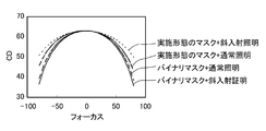
図3に、遮光部及び反射後部を含む本実施形態のマスクと、遮光部のみからなるパターンを有する通常のバイナリマスクとについて露光を行なった際のフォーカス変動に対するCD(線幅寸法)変化を示す。尚、通常照明の場合と、斜入射照明の場合とを共に示している。
FIG. 3 shows a CD (line width dimension) change with respect to a focus variation when exposure is performed on the mask of the present embodiment including the light-shielding portion and the reflection rear portion and a normal binary mask having a pattern including only the light-shielding portion. . Both the case of normal illumination and the case of oblique incidence illumination are shown.
ここで、例えばターゲット63nmに対して±10nmの寸法変動、つまり、63±10nmの範囲内の寸法を実現できるフォーカスの最大幅をDOFと定義する。これは、図3において、CDが53nm以上で且つ73nm以下となるフォーカスの幅として示される。図3に示す通り、バイナリマスクを用いる場合、斜入射照明との組み合わせではDOF=112nm、通常照明との組み合わせではDOF=117nmである。これに対し、本実施形態のフォトマスク40を用いる場合、通常照明との組み合わせではDOF=128nm、斜入射照明との組み合わせではDOF=146nmである。
Here, for example, the maximum width of the focus that can realize a dimensional variation of ± 10 nm with respect to the target 63 nm, that is, a size within the range of 63 ± 10 nm is defined as DOF. This is shown in FIG. 3 as the focus width at which the CD is 53 nm or more and 73 nm or less. As shown in FIG. 3, when using a binary mask, DOF = 112 nm in combination with oblique incidence illumination and DOF = 117 nm in combination with normal illumination. On the other hand, when the photomask 40 of this embodiment is used, DOF = 128 nm in combination with normal illumination and DOF = 146 nm in combination with oblique incidence illumination.
このように、フォトマスク40を用いると、バイナリマスクを用いる場合に比べて、フォーカス変動に対するCD変化が小さい。つまり、DOFが大きい。
Thus, when the photomask 40 is used, the CD change with respect to the focus fluctuation is small as compared with the case where the binary mask is used. That is, the DOF is large.
これに加えて、バイナリマスクの場合、斜入射照明を用いるよりも通常照明を用いる方がDOFは大きいのに対して、本実施形態のフォトマスクの場合、通常照明を用いるよりも斜入射照明を用いる方がDOFは大きい。これは、微細な密集パターンを形成するために斜入射照明を用いる際に、孤立スペースパターンについても同時に微細化することが可能であることを示している(バイナリマスクの場合、微細な密集パターンを形成するために斜入射照明を用いると、孤立スペースパターンについてはDOFが低下するので微細化が困難になる)。
In addition to this, in the case of the binary mask, the DOF is larger in the case of using the normal illumination than in the case of using the oblique illumination, whereas in the case of the photomask of the present embodiment, the oblique incidence illumination is used rather than using the normal illumination. The DOF is larger when used. This indicates that when oblique incidence illumination is used to form a fine dense pattern, it is possible to simultaneously refine the isolated space pattern (in the case of a binary mask, the fine dense pattern is reduced). If oblique incidence illumination is used to form an isolated space pattern, it becomes difficult to miniaturize the isolated space pattern because the DOF decreases.
次に、フォトマスク40における遮光部(12a及び12b)について更に説明する。遮光部の幅B1(図1(c)を参照)が大きくなるにつれて、半遮光部と開口部との間の光の干渉度が小さくなり、孤立スペース(16及び17)に関するDOFがバイナリマスクの挙動に近付く。つまり、孤立スペースに関するDOF拡大の効果が得られにくくなる。従って、DOFを大きくするためには、遮光部の幅B1をある程度の値以下に設定する必要がある。
Next, the light shielding portions (12a and 12b) in the photomask 40 will be further described. As the width B1 of the light-shielding portion (see FIG. 1C) increases, the degree of light interference between the semi-light-shielding portion and the opening decreases, and the DOF related to the isolated space (16 and 17) becomes smaller than that of the binary mask. Approach the behavior. That is, it becomes difficult to obtain the effect of DOF expansion related to the isolated space. Therefore, in order to increase the DOF, it is necessary to set the width B1 of the light shielding portion to a certain value or less.
図4に、遮光部の幅と、孤立スペースにおけるDOFとの関係を示す。ここでは、DOFは、図3の場合と同様に、例えばターゲット幅63nmに対して±10nm以内の寸法変動を実現できるフォーカスの最大幅として定義する。
FIG. 4 shows the relationship between the width of the light shielding part and the DOF in the isolated space. Here, as in the case of FIG. 3, DOF is defined as, for example, the maximum focus width that can realize a dimensional variation within ± 10 nm with respect to a target width of 63 nm.
図4に示す通り、遮光部の幅が極小さい範囲以外では、DOFを大きくする効果を得るためには遮光部の幅を小さくする必要がある。よって、具体例として、遮光部の幅が0.05×λ/NA(前提事項として説明した例によると、7nm)以上とすると共に、1.13×λ/NA(同じ例によると161nm)以下とすると、バイナリマスクと比較してDOFが10以上向上する。更に、遮光部の幅が0.12×λ/NA(同じ例によると17nm)以上とすると共に、0.63×λ/NA(同じ例によると90nm)以下とすることにより、20%以上のDOF向上が可能となる。この他にも、同様にして、図4から、DOFを所望量向上するために望ましい遮光部の幅B1の範囲を求めることが可能である。
As shown in FIG. 4, outside the range where the width of the light shielding portion is extremely small, it is necessary to reduce the width of the light shielding portion in order to obtain the effect of increasing the DOF. Therefore, as a specific example, the width of the light-shielding portion is 0.05 × λ / NA (7 nm according to the example described as the premise) or more and 1.13 × λ / NA (161 nm according to the same example) or less. Then, the DOF is improved by 10 or more compared to the binary mask. Furthermore, when the width of the light-shielding portion is set to 0.12 × λ / NA (17 nm according to the same example) or more and 0.63 × λ / NA (90 nm according to the same example) or less, 20% or more is achieved. The DOF can be improved. In addition, similarly, it is possible to obtain the range of the width B1 of the light-shielding portion that is desirable for improving the DOF by a desired amount from FIG.
この一方、遮光部の幅B1が小さすぎると、孤立スペース(開口部)を透過した光に対して半遮光部を透過した透過光の回り込みによる影響が強くなる。この結果、孤立スペースに対応する光強度の極小値が下がらず、孤立スペース部分のNILS(Normalized Image Log Slope)が悪化するという問題がある。従って、遮光部の幅B1は、NILSの観点から、一定の寸法以上に設定する必要がある。
On the other hand, if the width B1 of the light shielding part is too small, the influence of the transmitted light that has passed through the semi-light shielding part becomes strong against the light that has passed through the isolated space (opening). As a result, there is a problem that the minimum value of the light intensity corresponding to the isolated space does not decrease, and NILS (Normalized Image Log Slope) of the isolated space portion is deteriorated. Therefore, the width B1 of the light shielding portion needs to be set to a certain dimension or more from the viewpoint of NILS.
NILSは、次のように定義される。
NILS is defined as follows.
NILS = (δlnI/δx)×W
ここで、Iは光強度、(δlnI/δx)は光強度の対数勾配、Wはパターンの寸法であり、NILSの値が大きいほど、広い露光量余裕度を得ることができる。ArF露光によって形成する微細パターンの場合、NILSは、例えば1.3以上であることが好ましい。遮光部の幅を小さくすると、開口部近傍の暗部の光強度が下がらず、光強度の傾きが緩やかになる為、NILSは小さくなる。 NILS = (δlnI / δx) × W
Here, I is the light intensity, (δlnI / δx) is the logarithmic gradient of the light intensity, W is the pattern dimension, and the larger the NILS value, the wider the exposure allowance. In the case of a fine pattern formed by ArF exposure, NILS is preferably 1.3 or more, for example. When the width of the light shielding portion is reduced, the light intensity in the dark portion near the opening is not lowered, and the slope of the light intensity becomes gentle, so that NILS is reduced.
図5は、孤立スペースパターンに関して、遮光部の幅B1と、NILSとの関係を示した図である。
FIG. 5 is a diagram showing the relationship between the width B1 of the light shielding portion and NILS regarding the isolated space pattern.
微細プロセスにおいて、NILSの値は1.3以上であることが好ましい。図5から、遮光部の幅B1が0.13×λ/NA(前提事項の例の場合、18nm)以上にする必要があるとわかる。その他、所望のNILSを得るために必要な遮光部の幅B1について、図5から求めることができる。
In the fine process, the NILS value is preferably 1.3 or more. From FIG. 5, it can be seen that the width B1 of the light shielding portion needs to be 0.13 × λ / NA (18 nm in the case of the premise) or more. In addition, the width B1 of the light shielding portion necessary for obtaining a desired NILS can be obtained from FIG.
以上のようなDOF及びNILSに基づく点を合わせて考えると、遮光部の幅B1について、最大値はDOFにより決定され、最小値はNILSにより決定されることが分る。
Considering together the points based on DOF and NILS as described above, it can be seen that the maximum value is determined by DOF and the minimum value is determined by NILS for the width B1 of the light shielding portion.
具体例として、0.7×λ/NAよりも大きい幅L2を有するマスクパターンと、隣のマスクパターンとの間の距離(スペース寸法S1)が、0.5×λ/NAよりも小さいレイアウトのフォトマスク(図1(b)及び(c)のフォトマスク40)を考える。このとき、幅L2のマスクパターン14a及び14bに半遮光部13a及び13bを配置し、その周辺に、0.13×λ/NA以上で且つ1.13×λ/NA以下の幅を有する遮光部12a及び12bを配置する。これにより、十分なNILSを確保すると共に、孤立スペースのDOFを10%以上向上することができる。同様に、遮光部の幅を0.13×λ/NA以上で且つ0.63×λ/NA以下とすると、十分なNILSを確保すると共に、孤立スペースのDOFを20以上向上することができる。
As a specific example, the distance between the mask pattern having a width L2 larger than 0.7 × λ / NA and the adjacent mask pattern (space dimension S1) is smaller than 0.5 × λ / NA. Consider a photomask (photomask 40 in FIGS. 1B and 1C). At this time, the semi-light-shielding portions 13a and 13b are arranged in the mask patterns 14a and 14b having the width L2, and the light-shielding portions having a width of 0.13 × λ / NA or more and 1.13 × λ / NA or less around the periphery. 12a and 12b are arranged. As a result, sufficient NILS can be secured and the DOF of the isolated space can be improved by 10% or more. Similarly, when the width of the light shielding portion is 0.13 × λ / NA or more and 0.63 × λ / NA or less, sufficient NILS can be ensured and the DOF of the isolated space can be improved by 20 or more.
次に、半遮光部の幅について説明する。半遮光部の幅が小さいと、露光を行なった際に、半遮光部に対応する光強度が孤立スペースパターンに対応する光強度に対して小さくなる。この結果、光強度分布の周期性が十分に上がらず、DOF拡大の効果が得られにくくなる。これに関して、図6を参照して説明する。
Next, the width of the semi-light-shielding part will be described. If the width of the semi-light-shielding portion is small, the light intensity corresponding to the semi-light-shielding portion becomes smaller than the light intensity corresponding to the isolated space pattern when exposure is performed. As a result, the periodicity of the light intensity distribution is not sufficiently increased, and the effect of DOF expansion is difficult to obtain. This will be described with reference to FIG.
図6は、半遮光部の幅に対するDOFの関係をシミュレーションによって求めた結果を示す。図6から、半遮光部の幅が0.42×λ/NAよりも大きい場合(前提事項として説明した例によると、60nmよりも大きい場合)、半遮光部が存在しないバイナリマスクの例(半遮光部の幅が0nmの場合に相当する)と比較して、10%のDOF拡大が可能となることがわかる。更に、半遮光部の幅が0.98×λ/NAよりも大きい場合(前提事項として説明した例によると、140nmよりも大きい場合)、バイナリマスクと比較して20%のDOF拡大が可能となることがわかる。
FIG. 6 shows the result of the simulation of the relationship of DOF with respect to the width of the semi-light-shielding portion. From FIG. 6, when the width of the semi-light-shielding part is larger than 0.42 × λ / NA (according to the example described as the premise, it is larger than 60 nm), an example of the binary mask without the semi-light-shielding part (half It can be seen that the DOF can be enlarged by 10% compared to the case where the width of the light shielding portion is 0 nm. Furthermore, when the width of the semi-light-shielding part is larger than 0.98 × λ / NA (in the example described as the premise, it is larger than 140 nm), the DOF can be enlarged by 20% compared to the binary mask. I understand that
また、半遮光部の幅H1、遮光部の幅B1については、マスク作成の限界よりも大きな値にすることができるので、マスク作成が容易になり、コスト低減も可能である。
Also, since the width H1 of the semi-light-shielding portion and the width B1 of the light-shielding portion can be set to values larger than the limit of mask creation, mask creation is facilitated and cost can be reduced.
但し、以上に挙げた具体的な数値(各寸法についてn×λ/NAと表すときのnの値等)は、いずれも例示するものであり、これらに限定されるものではない。更に、露光光の波長、光源の形状、NA、M等が異なる場合にも、同様の方法により、望ましい値を求めることができる。
However, the specific numerical values given above (the value of n when expressed as n × λ / NA for each dimension, etc.) are only examples, and are not limited thereto. Furthermore, even when the wavelength of exposure light, the shape of the light source, NA, M, and the like are different, a desirable value can be obtained by the same method.
次に、本実施形態のフォトマスク40を用いたパターン形成方法について、その各工程を模式的に示す断面図である図7(a)~(d)を参照して説明する。
Next, a pattern forming method using the photomask 40 of the present embodiment will be described with reference to FIGS. 7A to 7D which are cross-sectional views schematically showing each step.
まず、図7(a)に示すように、シリコン等からなる基板100上に、金属膜、絶縁膜等の被加工膜101を形成する。続いて、図7(b)に示すように、被加工膜101上にポジ型のレジスト膜102を形成する。
First, as shown in FIG. 7A, a film to be processed 101 such as a metal film or an insulating film is formed on a substrate 100 made of silicon or the like. Subsequently, as shown in FIG. 7B, a positive resist film 102 is formed on the film 101 to be processed.
次に、図7(c)に示すように、フォトマスク40を用いて露光を行なう。例えば、ArFエキシマレーザー、KrFエキシマレーザー等を光源として露光光103を照射する。これにより、フォトマスク40の開口部(孤立スペース16及び17、密集マスクパターン15同士の間の領域等)を透過した透過光105によってレジスト膜102が感光され、結果として開口部に対応する潜像部分102aが形成される。
Next, as shown in FIG. 7C, exposure is performed using a photomask 40. For example, the exposure light 103 is irradiated using an ArF excimer laser, a KrF excimer laser, or the like as a light source. As a result, the resist film 102 is exposed to the transmitted light 105 that has passed through the openings of the photomask 40 ( isolated spaces 16 and 17, areas between the dense mask patterns 15 and the like), and as a result, a latent image corresponding to the openings. A portion 102a is formed.
この後、図7(d)に示すように、現像を行なうことにより潜像部分102aを除去し、レジスト膜102のうち感光されていない部分からレジストパターン106を得る。
Thereafter, as shown in FIG. 7D, development is performed to remove the latent image portion 102a, and a resist pattern 106 is obtained from a portion of the resist film 102 that is not exposed to light.
ここで、図7(c)の露光の際に、現像工程においてレジスト膜102が完全に溶解するに足りるだけの露光エネルギーが照射されるのは、潜像部分102aのみである。フォトマスク40におけるハーフトーン部(半遮光部13a、13b)を透過した透過光104は、開口部を透過した透過光105と同位相であるが、レジスト膜102を感光して潜像部分とするだけのエネルギーを有していない。従って、フォトマスク40の開口部に対応する部分のレジスト膜102のみが感光される。
Here, at the time of exposure in FIG. 7C, only the latent image portion 102a is irradiated with exposure energy sufficient to completely dissolve the resist film 102 in the development process. The transmitted light 104 transmitted through the halftone portions ( semi-shielding portions 13a and 13b) in the photomask 40 has the same phase as the transmitted light 105 transmitted through the opening, but the resist film 102 is exposed to form a latent image portion. Just don't have energy. Accordingly, only the resist film 102 corresponding to the opening of the photomask 40 is exposed.
前述のように、フォトマスク40において、幅L2が0.7×λ/NAよりも大きいマスクパターン14a及び14bが、近傍のパターンと0.5×λ/NA以下の間隔(スペース寸法S1)にて配置されている例を考える。この時、幅L2のパターン内部に、0.42×λ/NAよりも大きい幅の半遮光部を配置し、その周囲には幅が0.13×λ/NAよりも大きく、1.13×λ/NAよりも小さい遮光部を配置する。また、0.7×λ/NAよりも小さいライン幅L1を有する微細な密集マスクパターン15を、幅L2のパターンとの間隔もスペース寸法S1として配置する。これにより、開口部、遮光部、半遮光部の配置により露光時の光強度分布に明、暗、明、暗のような周期性を持たせることのできるフォトマスクとなっており、且つ、図4~6によって示した寸法の関係が実現する。
As described above, in the photomask 40, the mask patterns 14a and 14b having the width L2 larger than 0.7 × λ / NA are spaced from the neighboring patterns by 0.5 × λ / NA or less (space dimension S1). Consider an example where At this time, a semi-light-shielding portion having a width larger than 0.42 × λ / NA is disposed inside the pattern having the width L2, and the width thereof is larger than 0.13 × λ / NA, and 1.13 × A light shielding part smaller than λ / NA is arranged. Further, a fine dense mask pattern 15 having a line width L1 smaller than 0.7 × λ / NA is arranged with a space dimension S1 as an interval from the pattern of width L2. As a result, the photomask can be provided with periodicity such as bright, dark, bright, and dark in the light intensity distribution during exposure by the arrangement of the opening, the light-shielding part, and the semi-light-shielding part. The dimensional relationship indicated by 4-6 is realized.
このようなフォトマスク40を用い、微細な密集マスクパターン15を形成することを目的として斜入射照明を用いた露光を行なうと、孤立スペース16等のDOF拡大が可能になる。この結果、微細な密集パターンと、孤立スペースパターンとを共に精度良く同時に形成することができる。
When such photomask 40 is used and exposure using oblique incidence illumination is performed for the purpose of forming fine dense mask pattern 15, the DOF of isolated space 16 or the like can be enlarged. As a result, a fine dense pattern and an isolated space pattern can be formed simultaneously with high accuracy.
(変形例)
以下に、本実施形態のフォトマスクに関する各種変形例を説明する。 (Modification)
Hereinafter, various modifications related to the photomask of this embodiment will be described.
以下に、本実施形態のフォトマスクに関する各種変形例を説明する。 (Modification)
Hereinafter, various modifications related to the photomask of this embodiment will be described.
図8(a)は、本変形例において形成しようとしている例示的パターン51を示す平面図であり、図8(b)は、パターン51の形成に用いる例示的フォトマスク41を示す平面図であり、図8(c)は、図5(b)におけるVIIIc-VIIIc'線における断面図であり、図8(d)は、図5(b)におけるVIIId-VIIId'線における断面図である。ここで、図8(a)~(d)において、図1(a)~(c)と同等の構成要素には同じ符号を付している。
FIG. 8A is a plan view showing an exemplary pattern 51 to be formed in the present modification, and FIG. 8B is a plan view showing an exemplary photomask 41 used for forming the pattern 51. 8C is a cross-sectional view taken along line VIIIc-VIIIc ′ in FIG. 5B, and FIG. 8D is a cross-sectional view taken along line VIIId-VIIId ′ in FIG. 5B. Here, in FIGS. 8A to 8D, the same components as those in FIGS. 1A to 1C are denoted by the same reference numerals.
フォトマスク41においても、図1(b)のフォトマスク40と同様に、マスクパターン14a及び14bの内側に半遮光部13a及び13bを備え、その周囲に遮光部12a及び12bが配置されている。また、幅L2のマスクパターン14a及び14bがVc-Vc'線方向に(マスクパターン同士が孤立スペースを挟んで対向する方向に)スペース寸法S1を空けて並んでいる。
Similarly to the photomask 40 in FIG. 1B, the photomask 41 also includes semi-light-shielding portions 13a and 13b inside the mask patterns 14a and 14b, and the light-shielding portions 12a and 12b are arranged around it. Further, the mask patterns 14a and 14b having the width L2 are arranged with a space dimension S1 in the Vc-Vc ′ line direction (in a direction in which the mask patterns face each other with an isolated space therebetween).
しかしながら、VIIId-VIIId'線とは異なるVIIId-VIIId'線上において、マスクパターン14aは、マスクパターン14bと並ぶ配置にはならず、0.5×λ/NA×Mよりも大きいスペース寸法S2を空けてマスクパターン15aと並ぶ配置となっている。このように、マスクパターン14aのうち、隣のマスクパターンとの間隔が所定の値(λ、NA、Mにより定まる値、例えば前記の0.5×λ/NA×M)よりも大きい部分が存在し、このような部分については、半遮光部13aを配置しない構成になっている。
However, on the VIIId-VIIId ′ line different from the VIIId-VIIId ′ line, the mask pattern 14a is not arranged side by side with the mask pattern 14b, and a space dimension S2 larger than 0.5 × λ / NA × M is provided. The mask pattern 15a is arranged side by side. As described above, there is a portion of the mask pattern 14a where the distance from the adjacent mask pattern is larger than a predetermined value (a value determined by λ, NA, M, for example, 0.5 × λ / NA × M). In such a portion, the semi-light-shielding portion 13a is not disposed.
同様に、マスクパターン14bにおいても、マスクパターン14aとスペース寸法S1を空けて並ぶ部分に半遮光部13bが配置されるようになっている。
Similarly, also in the mask pattern 14b, the semi-light-shielding portion 13b is arranged in a portion aligned with the mask pattern 14a and the space dimension S1.
つまり、DOFが不足するスペース寸法S1の孤立スペースについては、マスクパターン内に半遮光部を配置し、且つ、DOF拡大が不要な大きさのスペース寸法S2を空けて配置された部分については半遮光部を配置していない。これにより、必要な箇所のDOFを拡大することができるとことに加えて、フォトマスクの加工が容易になると共に描画時間の短縮が可能になり、マスクコストの削減が実現する。
That is, for the isolated space having the space dimension S1 where the DOF is insufficient, the semi-light-shielding portion is disposed in the mask pattern, and the portion disposed with the space dimension S2 having a size that does not require DOF expansion is semi-light-shielded. The part is not arranged. Thereby, in addition to being able to enlarge the DOF at a necessary location, the photomask can be easily processed and the drawing time can be shortened, thereby reducing the mask cost.
次に、図9(a)は、他の例示的フォトマスク42を示す平面図であり、フォトマスク42は、図1(a)のパターンを形成するためのパターンを有する。また、図9(b)は、図9(a)におけるIXb-IXb'線による断面を示す図である。
Next, FIG. 9A is a plan view showing another exemplary photomask 42, and the photomask 42 has a pattern for forming the pattern of FIG. 1A. FIG. 9B is a diagram showing a cross section taken along line IXb-IXb ′ in FIG.
図1(b)のフォトマスク40の場合、マスクパターン14a及び14bの周縁部に遮光部12a及び12bが配置され、半遮光部13a及び13bは、一続きの領域として形成されている。これに対し、図9(a)のフォトマスク42の場合、遮光部12a及び12bはマスクパターン14a及び14bの内側にも形成され、半遮光部13a及び13bを複数の部分に分割している。
In the case of the photomask 40 in FIG. 1B, the light shielding portions 12a and 12b are arranged on the peripheral portions of the mask patterns 14a and 14b, and the semi-light shielding portions 13a and 13b are formed as a continuous region. On the other hand, in the case of the photomask 42 of FIG. 9A, the light shielding portions 12a and 12b are also formed inside the mask patterns 14a and 14b, and the semi-light shielding portions 13a and 13b are divided into a plurality of portions.
このようなフォトマスク42を用いて露光を行なうと、図10に示す通り、光強度分布における明、暗、明、暗の周期性を更に高めることができるので、孤立スペースのDOFを更に拡大することができる。
When exposure is performed using such a photomask 42, the periodicity of light, dark, bright, and dark in the light intensity distribution can be further enhanced as shown in FIG. 10, so that the DOF of the isolated space is further expanded. be able to.
図11には、図1(a)のパターンを形成するための更に別の例示的フォトマスク43を示している。フォトマスク43の場合、遮光部12a及び12bは、マスクパターン14a及び14bの周縁部に加えて、半遮光部13a及び13bの内側にも独立した島状に配置されている。この場合にも、図11のIXb-IXb'線による断面は図9(b)と同様になる。従って、フォトマスク43を用いて露光した場合の光強度分布における明暗は周期性が高くなり、DOF拡大を実現することができる。
FIG. 11 shows still another exemplary photomask 43 for forming the pattern of FIG. In the case of the photomask 43, the light shielding portions 12a and 12b are arranged in an independent island shape inside the semi-light shielding portions 13a and 13b in addition to the peripheral portions of the mask patterns 14a and 14b. Also in this case, the cross section taken along line IXb-IXb ′ in FIG. 11 is the same as FIG. 9B. Therefore, the light and darkness in the light intensity distribution when exposed using the photomask 43 has high periodicity, and the DOF expansion can be realized.
これらの他にも、孤立スペースパターンを挟んだマスクパターンの対向方向(例えば図9(a)におけるIXb-IXb'線の方向)について、半遮光部と遮光部とが交互に並ぶような配置とすることにより、DOFの拡大を図ることができる。例えば、半遮光部を囲む部分の遮光部の一部から、反対側の遮光部には達しない突出部が設けられている構成でもよい。
In addition to these, with respect to the opposing direction of the mask pattern with the isolated space pattern interposed therebetween (for example, the direction of the line IXb-IXb ′ in FIG. 9A), the semi-light-shielding portions and the light-shielding portions are arranged alternately. By doing so, it is possible to enlarge the DOF. For example, a configuration in which a protruding portion that does not reach the light shielding portion on the opposite side may be provided from a part of the light shielding portion that surrounds the semi-light shielding portion.
また、図12には、図1(a)のパターンを形成するための更に別の例示的フォトマスク44を示している。フォトマスク44の場合、半遮光部13a及び13bがマスクパターン14a及び14bの周縁部に配置されている点では図1(b)のフォトマスク40と同様である。但し、半遮光部13a及び13bを囲む遮光部12a及び12bについて、平面形状の凸コーナー部71における幅B2が、凹コーナー部72における幅B3よりも大きくなっている。これは、光近接効果補正(OPC:optical proximity correction)を考慮した形状である。このようなマスクパターンとすることにより、凸コーナー部71、凹コーナー部72のいずれにおいても、転写後のパターンの形状を改善(矩形性を向上)することができる。尚、密集マスクパターン15において、両端の幅が広くなっているのも同様の理由による。
FIG. 12 shows still another exemplary photomask 44 for forming the pattern of FIG. The photomask 44 is the same as the photomask 40 in FIG. 1B in that the semi-light-shielding portions 13a and 13b are arranged at the peripheral portions of the mask patterns 14a and 14b. However, regarding the light shielding portions 12a and 12b surrounding the semi-light shielding portions 13a and 13b, the width B2 of the planar convex corner portion 71 is larger than the width B3 of the concave corner portion 72. This is a shape considering optical proximity effect correction (OPC: optical proximity correction). By using such a mask pattern, the shape of the pattern after transfer can be improved (rectangularity improved) in both the convex corner portion 71 and the concave corner portion 72. In the dense mask pattern 15, the widths at both ends are wide for the same reason.
次に、図13及び図14は、半遮光部と遮光部とを設けるための他の構成を例示する模式的な断面図である。
Next, FIGS. 13 and 14 are schematic cross-sectional views illustrating other configurations for providing the semi-light-shielding portion and the light-shielding portion.
図1(c)に示すフォトマスク40の場合、透明基板11上に半遮光膜23を形成し、当該半遮光膜23上の必要箇所に遮光膜22を設けることによって、半遮光部13a及び13b、遮光部12a及び12bを構成している。
In the case of the photomask 40 shown in FIG. 1C, the semi-light-shielding portions 23a and 13b are formed by forming the semi-light-shielding film 23 on the transparent substrate 11 and providing the light-shielding film 22 at necessary locations on the semi-light-shielding film 23. The light shielding portions 12a and 12b are configured.
これに対し、図13の場合、透明基板11上の必要箇所に遮光膜22を形成し、当該遮光膜22上を覆うように、透明基板11上の必要箇所に半遮光膜23を形成することによって、半遮光部13a及び13b、遮光部12a及び12bを構成している。
On the other hand, in the case of FIG. 13, the light shielding film 22 is formed at a necessary location on the transparent substrate 11, and the semi-light shielding film 23 is formed at the necessary location on the transparent substrate 11 so as to cover the light shielding film 22. Thus, semi-light-shielding portions 13a and 13b and light-shielding portions 12a and 12b are configured.
更に、図14の場合、透明基板11上の必要箇所に半遮光膜23をパターン化し、当該半遮光膜23上及び透明基板11上の必要箇所に遮光膜22を形成することによって、半遮光部13a及び13b、遮光部12a及び12bを構成している。図1(c)の場合、半遮光膜23と遮光膜22とは側面が面一であるのに対し、図14の場合、遮光膜22は半遮光膜23の側面を覆うように形成され、透明基板11上に接している部分を有する。
Further, in the case of FIG. 14, the semi-light-shielding film 23 is patterned at a necessary portion on the transparent substrate 11, and the light-shielding film 22 is formed on the semi-light-shielding film 23 and the necessary portions on the transparent substrate 11, thereby forming a semi-light-shielding portion. 13a and 13b and light shielding parts 12a and 12b are configured. In the case of FIG. 1C, the side surfaces of the semi-light-shielding film 23 and the light-shielding film 22 are flush, whereas in the case of FIG. 14, the light-shielding film 22 is formed so as to cover the side surface of the semi-light-shielding film 23. A portion in contact with the transparent substrate 11 is provided.
いずれの場合も、半遮光膜23に関わりなく、遮光膜22の形成された範囲が遮光部となる。よって、図14において、遮光部の幅は、遮光部におけるスペースパターンの側のエッジから反対側のエッジまでとなる。
In any case, regardless of the semi-light-shielding film 23, the range where the light-shielding film 22 is formed becomes the light-shielding portion. Therefore, in FIG. 14, the width of the light shielding portion is from the edge on the space pattern side to the edge on the opposite side in the light shielding portion.
フォトマスクに遮光部及び半遮光部を設けるための構成として、図13及び図14のようになっていても良い。これらの場合にも、既に説明した通り、遮光部の幅を所定の値(例えば0.13×λ/NAよりも大きく、1.13×λ/NAよりも小さい値)とすることによって、孤立スペースパターンのDOF拡大が実現する。
As a configuration for providing the light-shielding portion and the semi-light-shielding portion in the photomask, it may be as shown in FIGS. Also in these cases, as already described, the width of the light shielding portion is set to a predetermined value (for example, a value larger than 0.13 × λ / NA and smaller than 1.13 × λ / NA), so that the isolation is achieved. The DOF expansion of the space pattern is realized.
本開示のフォトマスク及びこれを用いたパターン形成方法によると、サイドローブを発生させることなく密集パターン及び孤立スペースパターンを同時に精度良く形成することができ、且つ、フォトマスクの作成が容易になる。よって、素子分離等のSRAM部(密集パターン)とLogic部(孤立スペースパターン)が同時に存在する工程のパターン形成においても有用である。
According to the photomask of the present disclosure and the pattern forming method using the photomask, it is possible to simultaneously form a dense pattern and an isolated space pattern without generating side lobes, and to easily create a photomask. Therefore, it is also useful in pattern formation in a process in which an SRAM portion (dense pattern) and a logic portion (isolated space pattern) such as element isolation exist simultaneously.
11 透明基板
12a 遮光部
12b 遮光部
13a、13b 半遮光部
14a、14b マスクパターン
15 密集マスクパターン
15a マスクパターン
16、17 孤立スペース
22 遮光膜
23 半遮光膜
40~44 フォトマスク
50、51 パターン
71 凸コーナー部
72 凹コーナー部
100 基板
101 被加工膜
102 レジスト膜
102a 潜像部分
103 透過光
104 露光光
105 透過光
106 レジストパターン DESCRIPTION OFSYMBOLS 11 Transparent substrate 12a Light-shielding part 12b Light-shielding part 13a, 13b Semi-light-shielding part 14a, 14b Mask pattern 15 Dense mask pattern 15a Mask pattern 16, 17 Isolated space 22 Light-shielding film 23 Semi-light-shielding film 40-44 Photomask 50, 51 pattern 71 Convex Corner portion 72 Concave corner portion 100 Substrate 101 Work film 102 Resist film 102a Latent image portion 103 Transmitted light 104 Exposure light 105 Transmitted light 106 Resist pattern
12a 遮光部
12b 遮光部
13a、13b 半遮光部
14a、14b マスクパターン
15 密集マスクパターン
15a マスクパターン
16、17 孤立スペース
22 遮光膜
23 半遮光膜
40~44 フォトマスク
50、51 パターン
71 凸コーナー部
72 凹コーナー部
100 基板
101 被加工膜
102 レジスト膜
102a 潜像部分
103 透過光
104 露光光
105 透過光
106 レジストパターン DESCRIPTION OF
Claims (18)
- 透明基板と、
前記透明基板上に、スペースを挟んで対向する部分を有するように形成された第1マスクパターン及び第2マスクパターンを備え、
前記第1マスクパターンは、光を部分的に透過させる半遮光部と、遮光部とを含み、
前記第1マスクパターンにおいて、前記半遮光部は、前記遮光部を挟んで前記スペースと対向する部分を有するように配置され、
前記第1マスクパターンと前記第2マスクパターンとの対向方向について、
前記第1マスクパターンの寸法は、(0.7×λ/NA)×Mよりも大きく、
前記スペースの寸法は、(0.5×λ/NA)×M以下であることを特徴とするフォトマスク(但し、λは露光光の波長であり、NAは露光機の縮小投影光学系の開口数であり、Mは前記縮小投影光学系の倍率である)。 A transparent substrate;
A first mask pattern and a second mask pattern formed on the transparent substrate so as to have portions facing each other with a space in between,
The first mask pattern includes a semi-light-shielding part that partially transmits light, and a light-shielding part,
In the first mask pattern, the semi-light-shielding portion is arranged to have a portion facing the space with the light-shielding portion interposed therebetween,
About the opposing direction of the first mask pattern and the second mask pattern,
The dimension of the first mask pattern is larger than (0.7 × λ / NA) × M,
The size of the space is not more than (0.5 × λ / NA) × M, where λ is the wavelength of the exposure light, and NA is the aperture of the reduction projection optical system of the exposure machine And M is the magnification of the reduction projection optical system). - 請求項1のフォトマスクにおいて、
前記半遮光部及び前記遮光部は、前記第2マスクパターンにも他の半遮光部及び他の遮光部として含まれており、
前記第2マスクパターンにおいて、前記他の半遮光部は、前記他の遮光部を挟んで前記スペースと対向するように配置されていることを特徴とするフォトマスク。 The photomask of claim 1.
The semi-light-shielding part and the light-shielding part are also included in the second mask pattern as other semi-light-shielding parts and other light-shielding parts,
In the second mask pattern, the other semi-light-shielding portion is arranged to face the space with the other light-shielding portion interposed therebetween. - 請求項2のフォトマスクにおいて、
前記第1マスクパターンと前記第2マスクパターンとの対向方向について、
前記第2マスクパターンの寸法は、(0.7×λ/NA)×Mよりも大きいことを特徴とするフォトマスク。 The photomask of claim 2,
About the opposing direction of the first mask pattern and the second mask pattern,
The size of the said 2nd mask pattern is larger than (0.7 * (lambda) / NA) * M, The photomask characterized by the above-mentioned. - 請求項1~3のいずれか1つのフォトマスクにおいて、
前記第1マスクパターンと前記第2マスクパターンとの対向方向について、前記遮光部の寸法及び前記半遮光部の寸法は、λ、NA及びMに基づいて設定されていることを特徴とするフォトマスク(但し、λは露光光の波長であり、NAは露光機の縮小投影光学系の開口数であり、Mは前記縮小投影光学系の倍率である)。 The photomask according to any one of claims 1 to 3,
The photomask characterized in that the dimension of the light-shielding part and the dimension of the semi-light-shielding part are set based on λ, NA and M in the opposing direction of the first mask pattern and the second mask pattern. (Where λ is the wavelength of the exposure light, NA is the numerical aperture of the reduction projection optical system of the exposure machine, and M is the magnification of the reduction projection optical system). - 請求項4のフォトマスクにおいて、
前記遮光部の寸法は、(0.13×λ/NA)×M以上であることを特徴とするフォトマスク。 The photomask of claim 4,
A size of the light shielding portion is (0.13 × λ / NA) × M or more. - 請求項4又は5のフォトマスクにおいて、
前記遮光部の寸法は、(1.13×λ/NA)×M以下であることを特徴とするフォトマスク。 The photomask according to claim 4 or 5,
A size of the light shielding portion is (1.13 × λ / NA) × M or less. - 請求項4~6のいずれか1つのフォトマスクにおいて、
前記半遮光部の寸法は、(0.42×λ/NA)×M以上であることを特徴とするフォトマスク。 The photomask according to any one of claims 4 to 6,
The size of the said semi-light-shielding part is (0.42 * (lambda) / NA) * M or more, The photomask characterized by the above-mentioned. - 請求項1~7のいずれか1つのフォトマスクにおいて、
前記半遮光部は、前記スペースと同位相で光を透過させることを特徴とするフォトマスク。 The photomask according to any one of claims 1 to 7,
The semi-light-shielding portion transmits light with the same phase as the space. - 請求項1~8のいずれか1つのフォトマスクにおいて、
前記遮光部は、前記半遮光部を囲むように配置されていることを特徴とするフォトマスク。 The photomask according to any one of claims 1 to 8,
The photomask according to claim 1, wherein the light shielding portion is disposed so as to surround the semi-light shielding portion. - 請求項9のフォトマスクにおいて、
前記遮光部の幅は、前記半遮光部の凹コーナー部よりも前記半遮光部の凸コーナー部において広いことを特徴とするフォトマスク。 The photomask of claim 9,
The photomask according to claim 1, wherein a width of the light shielding portion is wider at a convex corner portion of the semi-light shielding portion than a concave corner portion of the semi-light shielding portion. - 請求項1~10のいずれか1つのフォトマスクにおいて、
前記半遮光部は、前記遮光部によって複数の部分に分割されていることを特徴とするフォトマスク。 The photomask according to any one of claims 1 to 10,
The semi-light-shielding portion is divided into a plurality of portions by the light-shielding portion. - 請求項1~11のいずれか1つのフォトマスクにおいて、
前記遮光部は、前記第1マスクパターンと前記第2マスクパターンとの対向方向について前記半遮光部に挟まれた部分を有することを特徴とするフォトマスク。 The photomask according to any one of claims 1 to 11,
The photomask having a portion sandwiched between the semi-shielding portions in a facing direction of the first mask pattern and the second mask pattern. - 請求項1~12のいずれか1つのフォトマスクにおいて、
前記半遮光部の光透過率は、前記半遮光部を透過した光が、感光領域を発生させる光強度よりも弱い光強度となるように設定されていることを特徴とするフォトマスク。 The photomask according to any one of claims 1 to 12,
The light transmittance of the semi-light-shielding portion is set so that light transmitted through the semi-light-shielding portion has a light intensity that is weaker than the light intensity that generates the photosensitive region. - 請求項1~13のいずれか1つのフォトマスクにおいて、
前記半遮光部は、前記遮光部を挟んで前記スペースと対向する部分のみに配置されていることを特徴とするフォトマスク。 The photomask according to any one of claims 1 to 13,
The photomask according to claim 1, wherein the semi-light-shielding portion is disposed only in a portion facing the space across the light-shielding portion. - 請求項1のフォトマスクにおいて、
前記第2マスクパターンは遮光部からなり、
前記第1マスクパターンと前記第2マスクパターンとの対向方向について、
前記第2マスクパターンの寸法は、(0.7×λ/NA)×M以下であることを特徴とするフォトマスク。 The photomask of claim 1.
The second mask pattern includes a light shielding portion,
About the opposing direction of the first mask pattern and the second mask pattern,
The size of the second mask pattern is (0.7 × λ / NA) × M or less. - 反射基板と、
前記反射基板上に、スペースを挟んで対向する部分を有するように形成された第1マスクパターン及び第2マスクパターンとを備え、
前記第1マスクパターンは、光を部分的に反射させる半反射部と、光を実質的に反射しない非反射部とを含み、
前記第1マスクパターンにおいて、前記半反射部は、前記非反射部を挟んで前記スペースと対向するように配置され、
前記第1マスクパターンと前記第2マスクパターンとの対向方向について、
前記第1マスクパターンの寸法は、(0.7×λ/NA)×Mよりも大きく、
前記スペースの寸法は、(0.5×λ/NA)×M以下であることを特徴とするフォトマスク(但し、λは露光光の波長であり、NAは露光機の縮小投影光学系の開口数であり、Mは前記縮小投影光学系の倍率である)。 A reflective substrate;
A first mask pattern and a second mask pattern formed on the reflective substrate so as to have portions facing each other with a space in between;
The first mask pattern includes a semi-reflective portion that partially reflects light and a non-reflective portion that does not substantially reflect light,
In the first mask pattern, the semi-reflective portion is disposed to face the space with the non-reflective portion interposed therebetween,
About the opposing direction of the first mask pattern and the second mask pattern,
The dimension of the first mask pattern is larger than (0.7 × λ / NA) × M,
The size of the space is not more than (0.5 × λ / NA) × M, where λ is the wavelength of the exposure light, and NA is the aperture of the reduction projection optical system of the exposure machine And M is the magnification of the reduction projection optical system). - 請求項1~16のいずれか1つのフォトマスクを用いるパターン形成方法において、
基板上にレジスト膜を形成する工程(a)と、
前記レジスト膜に、前記フォトマスクを介して露光光を照射する工程(b)と、
前記露光光が照射された前記レジスト膜を現像し、前記レジスト膜をパターン化する工程(c)とを備えることを特徴とするパターン形成方法。 A pattern forming method using the photomask according to any one of claims 1 to 16,
Forming a resist film on the substrate (a);
(B) irradiating the resist film with exposure light through the photomask;
Developing the resist film irradiated with the exposure light, and patterning the resist film (c). - 請求項17のパターン形成方法において、
前記工程(b)において、斜入射照明を用いることを特徴とするパターン形成方法。 In the pattern formation method of Claim 17,
In the step (b), oblique incidence illumination is used.
Priority Applications (1)
| Application Number | Priority Date | Filing Date | Title |
|---|---|---|---|
| US13/691,142 US20130095416A1 (en) | 2010-09-21 | 2012-11-30 | Photomask and pattern formation method |
Applications Claiming Priority (2)
| Application Number | Priority Date | Filing Date | Title |
|---|---|---|---|
| JP2010210672A JP2012068296A (en) | 2010-09-21 | 2010-09-21 | Photo mask and pattern formation method using the same |
| JP2010-210672 | 2010-09-21 |
Related Child Applications (1)
| Application Number | Title | Priority Date | Filing Date |
|---|---|---|---|
| US13/691,142 Continuation US20130095416A1 (en) | 2010-09-21 | 2012-11-30 | Photomask and pattern formation method |
Publications (1)
| Publication Number | Publication Date |
|---|---|
| WO2012039078A1 true WO2012039078A1 (en) | 2012-03-29 |
Family
ID=45873585
Family Applications (1)
| Application Number | Title | Priority Date | Filing Date |
|---|---|---|---|
| PCT/JP2011/002241 WO2012039078A1 (en) | 2010-09-21 | 2011-04-15 | Photomask, and pattern formation method using same |
Country Status (3)
| Country | Link |
|---|---|
| US (1) | US20130095416A1 (en) |
| JP (1) | JP2012068296A (en) |
| WO (1) | WO2012039078A1 (en) |
Families Citing this family (2)
| Publication number | Priority date | Publication date | Assignee | Title |
|---|---|---|---|---|
| JP6035884B2 (en) * | 2012-06-07 | 2016-11-30 | 大日本印刷株式会社 | Photomask manufacturing method |
| JP6315033B2 (en) * | 2016-07-09 | 2018-04-25 | 大日本印刷株式会社 | Photo mask |
Citations (5)
| Publication number | Priority date | Publication date | Assignee | Title |
|---|---|---|---|---|
| JP2002107909A (en) * | 2000-10-03 | 2002-04-10 | Nec Corp | Photomask and method for designing mask pattern of the same |
| WO2005040919A1 (en) * | 2003-10-23 | 2005-05-06 | Matsushita Electric Industrial Co., Ltd. | Photo mask, pattern formation method using the same, and mask data generation method |
| JP2006221078A (en) * | 2005-02-14 | 2006-08-24 | Renesas Technology Corp | Photomask, method for producing mask pattern, and method for forming pattern of semiconductor device |
| JP2008191364A (en) * | 2007-02-05 | 2008-08-21 | Elpida Memory Inc | Design method of mask pattern |
| JP2009075207A (en) * | 2007-09-19 | 2009-04-09 | Panasonic Corp | Photomask and pattern formation method using the same |
Family Cites Families (2)
| Publication number | Priority date | Publication date | Assignee | Title |
|---|---|---|---|---|
| US7897298B2 (en) * | 2006-03-06 | 2011-03-01 | Panasonic Corporation | Photomask, photomask fabrication method, pattern formation method using the photomask and mask data creation method |
| JP5193715B2 (en) * | 2008-07-18 | 2013-05-08 | 株式会社エスケーエレクトロニクス | Multi-tone photomask |
-
2010
- 2010-09-21 JP JP2010210672A patent/JP2012068296A/en active Pending
-
2011
- 2011-04-15 WO PCT/JP2011/002241 patent/WO2012039078A1/en active Application Filing
-
2012
- 2012-11-30 US US13/691,142 patent/US20130095416A1/en not_active Abandoned
Patent Citations (5)
| Publication number | Priority date | Publication date | Assignee | Title |
|---|---|---|---|---|
| JP2002107909A (en) * | 2000-10-03 | 2002-04-10 | Nec Corp | Photomask and method for designing mask pattern of the same |
| WO2005040919A1 (en) * | 2003-10-23 | 2005-05-06 | Matsushita Electric Industrial Co., Ltd. | Photo mask, pattern formation method using the same, and mask data generation method |
| JP2006221078A (en) * | 2005-02-14 | 2006-08-24 | Renesas Technology Corp | Photomask, method for producing mask pattern, and method for forming pattern of semiconductor device |
| JP2008191364A (en) * | 2007-02-05 | 2008-08-21 | Elpida Memory Inc | Design method of mask pattern |
| JP2009075207A (en) * | 2007-09-19 | 2009-04-09 | Panasonic Corp | Photomask and pattern formation method using the same |
Also Published As
| Publication number | Publication date |
|---|---|
| US20130095416A1 (en) | 2013-04-18 |
| JP2012068296A (en) | 2012-04-05 |
Similar Documents
| Publication | Publication Date | Title |
|---|---|---|
| US7790337B2 (en) | Photomask, pattern formation method using the same and mask data creation method | |
| US7332250B2 (en) | Photomask | |
| US7250248B2 (en) | Method for forming pattern using a photomask | |
| JP4754636B2 (en) | How to create mask data | |
| JP2002075823A (en) | Method of forming pattern of semiconductor device, method of designing pattern of photomask, photomask and manufacturing method thereof | |
| JP2009058877A (en) | Photomask and method for forming pattern using the same | |
| JP2009075207A (en) | Photomask and pattern formation method using the same | |
| JP3759914B2 (en) | Photomask and pattern forming method using the same | |
| US8007959B2 (en) | Photomask and pattern formation method using the same | |
| WO2012039078A1 (en) | Photomask, and pattern formation method using same | |
| JP2007018005A (en) | Photomask | |
| JP3759138B2 (en) | Photo mask | |
| JP3967359B2 (en) | Pattern formation method | |
| JP2004309958A (en) | Photomask, method of forming pattern using the photomask, and method of creating mask data | |
| JPWO2007102338A1 (en) | Photomask, method for producing the same, and pattern forming method using the photomask | |
| JP4314285B2 (en) | Photo mask | |
| JP3984626B2 (en) | Pattern formation method | |
| JP4314288B2 (en) | Photo mask | |
| JP2006039591A (en) | Method for forming pattern | |
| JP3322223B2 (en) | Phase shift mask | |
| JP2009237339A (en) | Photomask and method for manufacturing semiconductor device using the photomask | |
| JP3738234B2 (en) | Photomask, method for producing the same, and pattern forming method using the photomask | |
| JP4314286B2 (en) | Photo mask | |
| JP4009301B2 (en) | How to create mask data | |
| JP3984625B2 (en) | How to create mask data |
Legal Events
| Date | Code | Title | Description |
|---|---|---|---|
| 121 | Ep: the epo has been informed by wipo that ep was designated in this application |
Ref document number: 11826531 Country of ref document: EP Kind code of ref document: A1 |
|
| NENP | Non-entry into the national phase |
Ref country code: DE |
|
| 122 | Ep: pct application non-entry in european phase |
Ref document number: 11826531 Country of ref document: EP Kind code of ref document: A1 |