WO2012002032A1 - Ledパッケージ、照明装置、ledバックライト装置および液晶表示装置 - Google Patents
Ledパッケージ、照明装置、ledバックライト装置および液晶表示装置 Download PDFInfo
- Publication number
- WO2012002032A1 WO2012002032A1 PCT/JP2011/059915 JP2011059915W WO2012002032A1 WO 2012002032 A1 WO2012002032 A1 WO 2012002032A1 JP 2011059915 W JP2011059915 W JP 2011059915W WO 2012002032 A1 WO2012002032 A1 WO 2012002032A1
- Authority
- WO
- WIPO (PCT)
- Prior art keywords
- led
- terminal
- electrode terminal
- substrate
- backlight device
- Prior art date
- Legal status (The legal status is an assumption and is not a legal conclusion. Google has not performed a legal analysis and makes no representation as to the accuracy of the status listed.)
- Ceased
Links
Images



Classifications
-
- H—ELECTRICITY
- H10—SEMICONDUCTOR DEVICES; ELECTRIC SOLID-STATE DEVICES NOT OTHERWISE PROVIDED FOR
- H10H—INORGANIC LIGHT-EMITTING SEMICONDUCTOR DEVICES HAVING POTENTIAL BARRIERS
- H10H20/00—Individual inorganic light-emitting semiconductor devices having potential barriers, e.g. light-emitting diodes [LED]
- H10H20/80—Constructional details
- H10H20/85—Packages
- H10H20/857—Interconnections, e.g. lead-frames, bond wires or solder balls
-
- G—PHYSICS
- G02—OPTICS
- G02F—OPTICAL DEVICES OR ARRANGEMENTS FOR THE CONTROL OF LIGHT BY MODIFICATION OF THE OPTICAL PROPERTIES OF THE MEDIA OF THE ELEMENTS INVOLVED THEREIN; NON-LINEAR OPTICS; FREQUENCY-CHANGING OF LIGHT; OPTICAL LOGIC ELEMENTS; OPTICAL ANALOGUE/DIGITAL CONVERTERS
- G02F1/00—Devices or arrangements for the control of the intensity, colour, phase, polarisation or direction of light arriving from an independent light source, e.g. switching, gating or modulating; Non-linear optics
- G02F1/01—Devices or arrangements for the control of the intensity, colour, phase, polarisation or direction of light arriving from an independent light source, e.g. switching, gating or modulating; Non-linear optics for the control of the intensity, phase, polarisation or colour
- G02F1/13—Devices or arrangements for the control of the intensity, colour, phase, polarisation or direction of light arriving from an independent light source, e.g. switching, gating or modulating; Non-linear optics for the control of the intensity, phase, polarisation or colour based on liquid crystals, e.g. single liquid crystal display cells
- G02F1/133—Constructional arrangements; Operation of liquid crystal cells; Circuit arrangements
- G02F1/1333—Constructional arrangements; Manufacturing methods
- G02F1/1335—Structural association of cells with optical devices, e.g. polarisers or reflectors
- G02F1/1336—Illuminating devices
- G02F1/133602—Direct backlight
- G02F1/133603—Direct backlight with LEDs
-
- G—PHYSICS
- G02—OPTICS
- G02F—OPTICAL DEVICES OR ARRANGEMENTS FOR THE CONTROL OF LIGHT BY MODIFICATION OF THE OPTICAL PROPERTIES OF THE MEDIA OF THE ELEMENTS INVOLVED THEREIN; NON-LINEAR OPTICS; FREQUENCY-CHANGING OF LIGHT; OPTICAL LOGIC ELEMENTS; OPTICAL ANALOGUE/DIGITAL CONVERTERS
- G02F1/00—Devices or arrangements for the control of the intensity, colour, phase, polarisation or direction of light arriving from an independent light source, e.g. switching, gating or modulating; Non-linear optics
- G02F1/01—Devices or arrangements for the control of the intensity, colour, phase, polarisation or direction of light arriving from an independent light source, e.g. switching, gating or modulating; Non-linear optics for the control of the intensity, phase, polarisation or colour
- G02F1/13—Devices or arrangements for the control of the intensity, colour, phase, polarisation or direction of light arriving from an independent light source, e.g. switching, gating or modulating; Non-linear optics for the control of the intensity, phase, polarisation or colour based on liquid crystals, e.g. single liquid crystal display cells
- G02F1/133—Constructional arrangements; Operation of liquid crystal cells; Circuit arrangements
- G02F1/1333—Constructional arrangements; Manufacturing methods
- G02F1/1335—Structural association of cells with optical devices, e.g. polarisers or reflectors
- G02F1/1336—Illuminating devices
- G02F1/133602—Direct backlight
- G02F1/133608—Direct backlight including particular frames or supporting means
-
- H—ELECTRICITY
- H10—SEMICONDUCTOR DEVICES; ELECTRIC SOLID-STATE DEVICES NOT OTHERWISE PROVIDED FOR
- H10H—INORGANIC LIGHT-EMITTING SEMICONDUCTOR DEVICES HAVING POTENTIAL BARRIERS
- H10H20/00—Individual inorganic light-emitting semiconductor devices having potential barriers, e.g. light-emitting diodes [LED]
- H10H20/80—Constructional details
- H10H20/85—Packages
- H10H20/8506—Containers
Definitions
- the present invention relates to an LED package including an LED light source, an illumination device and an LED backlight device including the LED package, and a liquid crystal display device including the backlight device.
- LEDs Light Emitting Diodes
- the blue LED chip was developed, a white LED light source that emits white light by combining the blue LED chip and a phosphor that is excited by light from the LED chip and emits excitation light of a predetermined wavelength, A white LED light source that synthesizes white light using three primary color LED chips of a blue LED chip, a green LED chip, and a red LED chip has been developed.
- an LED illumination device provided with this white LED light source is used as a backlight of an illumination device, a liquid crystal display device or the like.
- a direct type backlight device in which a light source is disposed on the rear surface of the display screen, and a light guide plate is disposed on the rear surface of the display screen by arranging a light source on the side of the display screen.
- An edge light type backlight device is known in which light is incident on a light guide plate from a side portion of a display screen and light is emitted in a planar shape from a light emitting surface of the light guide plate while reflecting the light guide plate.
- the edge-light type backlight device is equipped with a light source on the side of the display screen and a plate-shaped light guide plate behind the display screen, making it easy to reduce the thickness of liquid crystal display devices, etc. Preferred for.
- the direct type backlight device is preferable because a light source is installed on the rear surface of the display screen to directly illuminate, so that high-intensity illumination is easy and control of light emission luminance for each area is easy.
- Each LED light source includes an LED package that is packaged by mounting an LED chip on a submount substrate and sealing it with a transparent resin or a transparent resin containing a predetermined phosphor.
- a plurality of packages are integrally installed on the LED mounting substrate to form a light emitting member having a predetermined shape.
- a large number of LED mounting boards on which a plurality of LED packages are mounted are arranged in parallel to constitute a lighting device having a large light emitting area such as a direct type backlight device. Therefore, when the LED package is mounted or replaced, the LED mounting substrate on which the plurality of LED packages are mounted is performed as a unit.
- the main board on which the LED mounting boards are arranged side by side has been devised to facilitate the attachment / detachment of the respective LED mounting boards.
- the LEDs and the electrical components necessary to drive the LEDs There has already been disclosed a backlight device in which a sub-printed board on which is integrally mounted is easily attached to and detached from a parent board (see, for example, Patent Document 1).
- the LED mounting board on which the LED package is mounted can be easily attached to and detached from the main board, the mounting efficiency is improved and the replacement work is also easy.
- the LED mounting board on which the LED package is mounted can be easily attached to and detached from the main board, the mounting efficiency is improved and the replacement work is also easy.
- each LED package has a configuration that can be easily replaced individually so that it can be performed.
- the LED light source is composed of an LED package in which a submount substrate, an LED chip, a sealing resin, and an electrode terminal are assembled and integrated, and the LED package can be individually attached to and detached from the LED mounting substrate.
- a configuration is preferable.
- the present invention is configured to be individually detachable from an LED mounting board in an illumination device using LEDs, a direct type LED backlight device, and a liquid crystal display device including the backlight device.
- An LED package is provided, and an LED mounting board on which the LED package is mounted is provided side by side to provide an illumination device and an LED backlight device that are excellent in mounting efficiency and economy, and the manufacturing cost can be reduced by using the backlight device.
- An object is to provide a liquid crystal display device that can be reduced.
- the present invention provides an LED chip, a submount substrate on which the LED chip is mounted, an electrode terminal for driving the LED chip, and a sealing resin for sealing the LED chip.
- the electrode terminal includes an LED side cathode terminal and an LED side anode terminal, and both of these terminals are provided on the back surface side of the submount substrate opposite to the LED chip mounting surface.
- the cathode terminal is a conical screw-like terminal provided on the side surface of the male electrode terminal, and the anode terminal is provided at the top of the truncated cone It is characterized by being a planar terminal.
- the female electrode terminal connected to the male electrode terminal included in the LED package is provided on the substrate side to which the LED package is attached, and the male LED side electrode terminal is screwed into the female substrate side electrode terminal.
- the respective cathode terminals and anode terminals can be electrically connected. Therefore, a detachable LED package can be obtained through a truncated cone electrode terminal.
- the LED package further includes an engaged portion to which an attachment connected to a detachable tool is engaged. According to this configuration, since the attachment / detachment operation of the LED package can be performed by engaging the attachment included in the attachment / detachment tool with the engaged portion of the LED package, the attachment / detachment operation of the LED package can be automated.
- the engaged portion is an outer shape outer frame of the submount substrate, and the outer frame has an outer shape that fits into an engagement recess included in the attachment. It is characterized by that. According to this configuration, the attachment / detachment operation of the LED package can be performed by fitting the attachment to the outer frame of the submount substrate.
- the engaged portion is a solidified outer shape of the sealing resin, and the solidified outer shape has an outer shape that fits into an engagement concave portion of the attachment. It is characterized by. According to this configuration, the attachment / detachment operation of the LED package can be performed by fitting the attachment into the outer shape of the sealing resin.
- the present invention is characterized in that in the LED package having the above-described configuration, a diffusion lens is mounted on the top of the sealing resin, and the diffusion lens has an outer shape that fits into an engagement recess included in the attachment. According to this configuration, the attachment / detachment operation of the LED package can be performed individually by fitting the attachment to the outer shape of the diffusing lens.
- a light emitting surface is formed by arranging a plurality of LED mounting boards on which a plurality of LED packages according to any one of claims 1 to 5 are mounted, and the LED mounting board is a male type provided in the LED package.
- a female electrode terminal that is screwed to the electrode terminal is provided, and the female electrode terminal has an inner peripheral side surface portion screwed to an LED-side cathode terminal provided on a frustoconical side surface of the male electrode terminal.
- the illumination device is a substrate-side cathode terminal and the bottom surface of the female electrode terminal is a substrate-side anode terminal.
- an LED backlight device for irradiating light emitted from an LED from behind a liquid crystal panel, wherein an LED mounting substrate on which a plurality of LED packages according to any one of claims 1 to 5 are mounted is provided in parallel.
- a light emitting surface is formed, and the LED mounting substrate includes a female electrode terminal screwed into a male electrode terminal included in the LED package, and the female electrode terminal includes an inner peripheral side surface of the male electrode terminal.
- a substrate-side cathode terminal screwed into an LED-side cathode terminal provided on a frustoconical side surface of the die electrode terminal is used, and a bottom surface portion of the female electrode terminal is a substrate-side anode terminal.
- the male electrode terminal included in the LED package and the female electrode terminal provided on the LED mounting board can be screwed together to mount each LED package on the LED mounting board.
- an LED backlight device having excellent mounting efficiency and economy can be obtained by arranging LED mounting substrates on which individually detachable LED packages are mounted to form a light emitting surface.
- an anode backlight terminal can be automatically connected to each other by an operation of screwing and mounting a conical screw-like cathode terminal, and an LED backlight device that can be easily mounted can be obtained.
- the engagement portion of the attachment connected to the attaching / detaching tool is engaged with the engaged portion included in the LED package, so that the plurality of LED mounting boards are provided.
- the LED packages can be individually attached to and detached from the LED mounting substrate by using the attachment / detachment tool in a state of being arranged in parallel. According to this configuration, since the LED package can be automatically attached / detached using the attaching / detaching tool having a predetermined attachment, an LED backlight device that can be mounted more easily can be obtained.
- the engaged portion may be an outer frame of a submount substrate included in the LED package, a solidified outer shape of a sealing resin, or an outer shape of a diffusion lens.
- These outer shapes are outer shapes that fit into engaging recesses of the attachment.
- the attachment / detachment tool can be mounted by engaging the attachment with the outer frame of the submount substrate or by engaging the attachment with the solidified outer shape of the sealing resin. ⁇ ⁇ Attaching / detaching operation using a tool for removal can be performed.
- the present invention is characterized in that a liquid crystal display device including a liquid crystal panel and the LED backlight device according to any one of claims 7 to 10 is provided. According to this configuration, it is possible to obtain a liquid crystal display device that can reduce the manufacturing cost by using a backlight device that is easy to attach and detach individual LED packages and is excellent in mounting efficiency and economy.
- each LED package is individually connected via the truncated cone-shaped terminal. It becomes a detachable configuration. Therefore, it is possible to obtain an illumination device and an LED backlight device that are excellent in mounting efficiency and economy by arranging the LED mounting substrate on which the LED package is mounted, and the manufacturing cost is reduced by using the backlight device. A possible liquid crystal display device can be obtained.
- the LED package 1 shown in FIG. 1 includes a submount substrate 11, an LED chip 12 mounted on the submount substrate 11, and a sealing resin 13 for sealing the LED chip 12.
- an electrode terminal TA for driving the LED chip 12 is provided on the back surface side of the submount substrate 11 opposite to the LED chip mounting surface.
- the electrode terminal TA is a male electrode terminal, and is connected to a female electrode terminal TB provided on the LED mounting substrate side.
- the LED package 1 can be easily attached to and detached from the LED mounting substrate via these male and female electrode terminals.
- Each electrode terminal includes a cathode terminal and an anode terminal.
- the electrode terminal TA of the LED package 1 is a male electrode terminal projecting in a truncated cone shape
- the LED side cathode terminal 14A Is a conical screw terminal provided on the side surface of the truncated cone
- the LED side anode terminal 15A is a planar terminal provided on the top of the truncated cone.
- the electrode terminal TB provided on the LED mounting substrate side is a female (female screw type) electrode terminal that fits into a male (male screw type) electrode terminal TA, and the inner peripheral side surface portion is formed on the substrate.
- the side cathode terminal 14B is used, and the bottom part is the substrate side anode terminal 15B.
- the LED side cathode terminal 14A and the LED side anode terminal 15A are each electrically connected to electrodes formed on the submount substrate, and a predetermined LED is connected via the electrode terminal TB on the LED mounting substrate side. A drive path is formed.
- the male conical screw-like electrode terminal TA is mounted so as to be screwed into the female electrode terminal TB, and the LED-side cathode terminal 14A and the substrate-side cathode terminal 14B provided on the side screw portion. And electrically connect. Further, when screwed to the end, the LED side anode terminal 14B and the substrate side anode terminal 15B come into contact with each other and are electrically connected.
- either one or both of the LED side anode terminal 14B and the substrate side anode terminal 15B may be configured to have elasticity in the abutting direction.
- the connection configuration includes the male conical screw electrode terminal TA and the female electrode terminal TB, the LED package is detachable via the truncated cone electrode terminal.
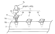
- each LED package 1 is detachably attached to the electrode terminal on the LED mounting substrate side, each LED package 1 can be individually detached and attached. Therefore, as shown in FIG. 2, even after a plurality of LED packages 1 (1 ⁇ / b> A, 1 ⁇ / b> B, 1 ⁇ / b> C...) Are incorporated in the mounting substrate 2 to form an integrated lighting device or light emitting device, each LED package 1. Can be removed individually and replaced with another new LED package.
- the LED package 1 is configured to include an engaged portion to which the attachment AT connected to the attachment / detachment tool TL such as an electric screwdriver is engaged, the attachment AT included in the attachment / detachment tool TL is the LED package 1. Since the attachment / detachment operation can be performed by being engaged with the engaged portion, the attachment / detachment operation can be automated, which is preferable.
- the engaged portion with which the attachment AT is engaged is preferably disposed on the upper surface side when the LED package 1 is mounted on the mounting substrate 2, in this embodiment, the submount substrate 11 shown in FIG.
- the example using an outer frame and the example using the solidified outer shape of the sealing resin 13 shown in FIG. 3B are employed.
- a submount substrate 11A having a polygonal outer frame with a predetermined shape is used, and an attachment AT1 having an engagement recess ATa that engages with the outer frame is used.
- the outer outer frame may be, for example, a quadrangle or a hexagon, and is not particularly limited.
- the sealing resin 13A having a polygonal solidified outer shape of a predetermined shape is used, and an attachment AT2 having an engagement recess ATb that engages with the solidified external shape is used.
- the shape of the solidified outer shape may be, for example, a quadrangle or a hexagon, and is not particularly limited.
- the diffusing lens may have an outer shape that fits into an engaging recess of the attachment AT.
- the attachment AT can be fitted into the outer shape of the diffusing lens and the LED package 1 can be attached and detached individually.
- the engaged portion provided in the LED package 1 may be other than the outer frame of the submount substrate, the solidified outer shape of the sealing resin, or the outer shape of the diffusing lens, for example, on the upper surface of the submount substrate.
- Engaging projections that engage with these fitting recesses (or projections) by providing fitting recesses (or projections) or fitting recesses (or projections) on the outer surface of the sealing resin. It is good also as a structure using the attachment provided with the part (or recessed part).
- the lighting device using the LED package 1 described above can detachably mount the LED packages 1 individually on the LED mounting substrate. Therefore, it is possible to form a light emitting surface having a predetermined area by arranging LED mounting substrates each having an individually detachable LED package mounted thereon, which is preferable as a lighting device having excellent mounting efficiency and economy.
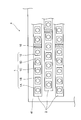
- the LED backlight device using the LED package 1 according to the present embodiment has, as shown in FIG. 4, for example, a connector 2 that is mounted on a mounting board 2 on which a predetermined number, for example, five LED packages 1 (1A to 1E) are mounted.
- the LED backlight device 4 having a predetermined area is formed by connecting through 16 and extending in a row and arranging a plurality of stages.
- the LED backlight device 4 in which the plurality of LED packages 1 are arranged at predetermined pitches in the vertical and horizontal directions is configured in units of a mounting substrate 2 on which a predetermined number, for example, five LED packages 1 are mounted. . Therefore, it can be attached and detached for each mounting substrate 2, mounting efficiency for mounting the LED package 1 on the LED backlight device 4 is improved, and replacement work is also facilitated.
- the LED package 1 according to the present embodiment is configured to be individually detachable from the mounting substrate 2, the LED package 1 can be mounted without removing the mounting substrate 2 installed on the LED backlight device 4. It can be detached and attached independently.
- the LED backlight device 4 excellent in mounting efficiency and economy can be obtained by arranging the LED mounting substrates 2 on which the individually detachable LED packages 1 are mounted in parallel. it can.
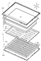
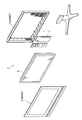
- a liquid crystal display device 6 using the above backlight device 4 as a direct backlight is configured as shown in FIG. Moreover, this liquid crystal display device 6 can be used as a display part of the liquid crystal television 7 shown in FIG. Such a liquid crystal television 7 can be said to be a television receiver since it receives a television broadcast signal and projects an image.
- the liquid crystal display device 6 includes a liquid crystal panel 5, an LED backlight device 4 for supplying light to the liquid crystal panel 5, and a housing HG (front housing HG1 and rear housing HG2) sandwiching them. And including.
- an active matrix substrate 51 including a switching element such as a TFT (Thin Film Transistor) and an opposing substrate 52 facing the active matrix substrate 51 are bonded together with a sealant (not shown). Then, liquid crystal (not shown) is injected into the gap between the substrates 51 and 52.
- a switching element such as a TFT (Thin Film Transistor)
- an opposing substrate 52 facing the active matrix substrate 51 are bonded together with a sealant (not shown). Then, liquid crystal (not shown) is injected into the gap between the substrates 51 and 52.
- a polarizing film 53 is attached to the light receiving surface side of the active matrix substrate 51 and the emission side of the counter substrate 52. And the above liquid crystal display panel 5 displays an image using the change of the transmittance
- the LED backlight device 4 positioned immediately below the liquid crystal display panel 5 includes an LED module MJ, a backlight chassis 41, a reflection sheet 42, a diffusion plate 43, a prism sheet 44, and a lens sheet 45.
- the LED module MJ is configured by mounting a plurality of LED packages 1 on the mounting surface 21U of the LED mounting substrate 21.
- the LED mounting substrate 21 is a plate-like and rectangular substrate like the LED mounting substrate 2 described above, and a plurality of electrodes (not shown) are arranged on the mounting surface 21U. Then, the packaged LED package 1 is mounted on these electrodes. Each LED package 1 is mounted with an LED chip via a submount substrate. The electrode and the LED chip are electrically connected via the submount substrate.
- a resist film (not shown) serving as a protective film is formed on the mounting surface 21U of the LED mounting substrate 21.
- This resist film is, for example, white having reflectivity. This is because even if light is incident on the resist film, the light is reflected by the resist film and tends to go outside, thereby eliminating the cause of unevenness in the amount of light due to light absorption by the mounting substrate 21.
- a relatively long mounting substrate 21 on which the LED packages 1 are mounted in a row is mounted.
- the rows of the five LED packages 1 and the row of the eight LED packages 1 are arranged so as to form a row of 13 LED packages 1, and further, with respect to the direction in which the 13 LED packages 1 are arranged.
- the two types of mounting boards 21 are also arranged in the intersecting (orthogonal) direction (note that the arrangement intervals of the LED packages 1 are equal).
- the arrangement pattern and the number of LED light sources arranged are appropriately changed according to the size of the screen and the required luminance.
- the LED package 1 is arranged in a lattice shape (in other words, the LED module MJ is planar), and light from these LED packages 1 is mixed to generate planar light (for convenience, different types of light are used).
- the direction in which the mounting boards 21 are arranged is the X direction
- the direction in which the same kind of mounting boards 21 are arranged is the Y direction
- the direction intersecting the X direction and the Y direction is the Z direction).
- the backlight chassis 41 is a box-shaped member, for example, and accommodates the plurality of LED modules MJ by spreading the LED modules MJ on the bottom surface 41B.
- the bottom surface 41B of the backlight chassis 41 and the LED mounting board 21 of the LED module MJ are connected via a rivet (not shown).
- a reflection sheet 42, a diffusion plate 43, a prism sheet 44, and a lens sheet 45 are stacked in this order.
- the reflection sheet 42 is an optical sheet having a reflection surface 42U, and covers the plurality of LED modules MJ with the back surface of the reflection surface 42U facing. However, the reflection sheet 42 includes a through hole 42H that matches the position of the LED package 1, and exposes the light emitting surface of the LED package 1 from the reflection surface 42U.
- the presence of the reflection sheet 42 causes the light of the LED package 1 to travel toward the diffusion plate 43 facing the reflection surface 42U without loss.
- the diffusion plate 43 is an optical sheet that overlaps the reflection sheet 42 and diffuses the light emitted from the LED module MJ and the reflection light from the reflection sheet 42U. That is, the diffusion plate 43 diffuses the planar light formed by the plurality of LED modules MJ (in other words, the plurality of LED packages 1 arranged in a matrix) and spreads the light over the entire liquid crystal display panel 5. .
- the prism sheet 44 is an optical sheet that overlaps the diffusion plate 43.
- the prism sheet 44 arranges, for example, triangular prisms extending in one direction (linear) in a direction intersecting with one direction in the sheet surface. Thereby, the prism sheet 44 deflects the radiation characteristic of the light from the diffusion plate 43.
- the prisms extend along the Y direction in which the LED packages 1 are arranged in a small number, and are arranged in the X direction in which the LED packages 1 are arranged in a large number.
- the lens sheet 45 is an optical sheet that overlaps the prism sheet 44.
- the lens sheet 45 disperses the fine particles that refract and scatter light inside. Thereby, the lens sheet 45 suppresses the light / dark difference (light quantity unevenness) without locally condensing the light from the prism sheet 44.
- the LED backlight device 4 as described above supplies the planar light formed by the plurality of LED modules MJ to the liquid crystal panel 5 through the plurality of optical sheets 43 to 45.
- the non-light-emitting liquid crystal panel 5 receives the light (backlight light) from the LED backlight device 4 and improves the display function.
- a plurality of LED packages 1 are arranged in, for example, a lattice shape or a zigzag shape to form a planar light emitter. Therefore, if defective products are mixed in the LED package 1 which is a point light source or a failure occurs, a predetermined light emission intensity cannot be obtained, which causes a reduction in display quality.
- an LED package It is preferable that each can be attached and detached individually. Therefore, by using the LED package 1 that is provided with a conical screw-like electrode terminal and can be individually attached to and detached from the LED mounting substrate, an LED backlight device 4 that is excellent in mounting efficiency and economy can be obtained.
- the liquid crystal display device 6 capable of reducing the manufacturing cost can be obtained using this backlight.
- the LED package 1 is provided with the conical screw-shaped cathode terminal and the planar anode terminal provided on the top of the truncated cone.
- the LED packages can be individually detached.
- the LED mounting substrate on which the LED package 1 is mounted it is possible to obtain an illumination device and an LED backlight device that are excellent in mounting efficiency and economy, and the manufacturing cost is reduced by using the backlight device.
- a possible liquid crystal display device can be obtained.
- the LED package and the LED backlight device according to the present invention use a large number of LED packages, reduce the manufacturing cost, stabilize the display quality, and improve the reliability.
- the LED backlight device can be suitably used.
Landscapes
- Physics & Mathematics (AREA)
- Nonlinear Science (AREA)
- Mathematical Physics (AREA)
- Chemical & Material Sciences (AREA)
- Crystallography & Structural Chemistry (AREA)
- General Physics & Mathematics (AREA)
- Optics & Photonics (AREA)
- Planar Illumination Modules (AREA)
- Liquid Crystal (AREA)
Abstract
LEDを用いた照明装置や直下型のLEDバックライト装置およびこのバックライト装置を備える液晶表示装置において、LED実装基板に個別に着脱自在な構成とされるLEDパッケージを提供し、このLEDパッケージを搭載したLED実装基板を並設することで実装効率と経済性に優れた照明装置やLEDバックライト装置を提供し、このバックライト装置を用いて製造コストを低減可能な液晶表示装置を提供するために、円錐螺子状のカソード端子とこの円錐台の頂部に設ける平面状のアノード端子とを備える雄型電極端子TAを有するLEDパッケージ1とし、LED実装基板に、この雄型電極端子に螺合する雌型電極端子TBを設け、円錐螺子状の接続端子を介して、それぞれのLEDパッケージ1が個別に着脱自在となる構成の照明装置およびLEDバックライト装置4とした。
Description
本発明は、LED光源を備えたLEDパッケージ、このLEDパッケージを備えた照明装置やLEDバックライト装置、およびこのバックライト装置を備えた液晶表示装置に関する。
近年、発光効率の向上や発光量の増加と共に、寿命が長く消費電力が小さくて、環境にやさしいとされるLED(Light Emitting Diode:発光ダイオード)を用いた照明装置が実用化されつつある。また、青色LEDチップが開発されて以来、この青色LEDチップと、このLEDチップからの光に励起されて所定波長の励起光を発光する蛍光体と、を組み合わせて白色発光する白色LED光源や、青色LEDチップと緑色LEDチップと赤色LEDチップとの三原色のLEDチップを用いて白色光を合成する白色LED光源が開発されている。
そのために、照明装置や液晶表示装置などのバックライトとして、この白色LED光源を配設したLED照明装置が用いられている。また、液晶表示装置などのバックライトとしては、表示画面の後面に光源を配置する直下型のバックライト装置と、表示画面の側部に光源を配置し表示画面の後面に導光板を設置して、表示画面の側部から導光板に光を入射して、導光板内を反射させながら導光板の発光面から面状に発光させるエッジライト型のバックライト装置が知られている。
エッジライト型のバックライト装置は、表示画面の側部に光源部を設け、表示画面の後方に板状の導光板を設置する構成なので、薄型化が容易であり、液晶表示装置などの薄型化にとって好ましい。また、直下型のバックライト装置は、表示画面の後面に光源を設置して直に照明しているので、高輝度照明が容易であり、発光輝度のエリア毎の制御も容易となって好ましい。
また、それぞれのLED光源は、サブマウント基板にLEDチップを搭載してその上を透明樹脂、あるいは所定の蛍光体を配合した透明樹脂で封止してパッケージ化されたLEDパッケージからなり、このLEDパッケージを、LED実装基板に複数一体に設置して所定形状の発光部材を形成している。
また、複数のLEDパッケージを搭載したLED実装基板を多数並設して、直下型バックライト装置等の大きな発光面積の照明装置を構成する。そのために、LEDパッケージを装着したり交換したりする際には、複数のLEDパッケージが搭載されたLED実装基板を単位として行う。
そのために、LED実装基板を並設するメイン基板に対して、それぞれのLED実装基板の着脱を容易とするための工夫がなされており、例えば、LEDとこのLEDを駆動するのに必要な電気部品を一体に装着したサブプリント基板を親基板に対して着脱容易としたバックライト装置が既に公開されている(例えば、特許文献1参照)。
LEDパッケージを搭載したLED実装基板がメイン基板に着脱容易であれば、実装効率がよくなり、交換作業も容易となる。しかし、1枚のLED実装基板に複数のLEDパッケージを搭載している場合は、1個のLEDパッケージに不良が生じるとLED実装基板単位で交換する必要が生じるので、問題のないLEDパッケージまで交換することになってしまい不経済となる。
また、LED照明装置やLEDバックライト装置の生産性を上げるためには、複数のLEDパッケージを搭載したLED実装基板を一体的に装着可能であるだけではなく、不良なLEDパッケージは直ちに良品と交換できるように、それぞれのLEDパッケージを個別に交換容易な構成であることが好ましい。
そのために、LED光源を、サブマウント基板とLEDチップと封止樹脂と電極端子とを組み付けて一体化したLEDパッケージから構成し、さらに、このLEDパッケージをLED実装基板に対して個別に着脱自在な構成とすることが好ましい。
そこで本発明は、上記問題点に鑑み、LEDを用いた照明装置や直下型のLEDバックライト装置およびこのバックライト装置を備える液晶表示装置において、LED実装基板に個別に着脱自在な構成とされるLEDパッケージを提供し、このLEDパッケージを搭載したLED実装基板を並設することで実装効率と経済性に優れた照明装置やLEDバックライト装置を提供し、このバックライト装置を用いて製造コストを低減可能な液晶表示装置を提供することを目的とする。
上記目的を達成するために本発明は、LEDチップと、該LEDチップを実装するサブマウント基板と、前記LEDチップを駆動するための電極端子と、前記LEDチップを封止する封止樹脂とを備えてパッケージ化されたLEDパッケージにおいて、前記電極端子がLED側カソード端子とLED側アノード端子とを備え、これらの両端子を前記サブマウント基板の前記LEDチップ実装面とは反対側の裏面側に円錐台状に突設した雄型電極端子として設けると共に、前記カソード端子は、前記雄型電極端子の側面に設けられた円錐螺子状端子であり、前記アノード端子は、前記円錐台の頂部に設けられた平面状端子とされていることを特徴としている。
この構成によると、LEDパッケージを取り付ける基板側に、LEDパッケージが備える雄型電極端子と接続する雌型の電極端子を設け、雄型のLED側電極端子を雌型の基板側電極端子にねじ込むようにして装着して、それぞれのカソード端子とアノード端子とを電気的に接続することができる。そのために、円錐台状の電極端子を介して着脱自在なLEDパッケージを得ることができる。
また本発明は上記構成のLEDパッケージにおいて、前記LEDパッケージは、さらに、着脱用工具に接続されるアタッチメントが係合する被係合部を備えていることを特徴としている。この構成によると、着脱用工具が備えるアタッチメントをLEDパッケージの被係合部に係合させて着脱操作を行うことができるので、LEDパッケージの着脱操作の自動化を図ることができる。
また本発明は上記構成のLEDパッケージにおいて、前記被係合部は、前記サブマウント基板の外形外枠であって、該外枠が前記アタッチメントが有する係合凹部に嵌合する外形形状とされることを特徴としている。この構成によると、サブマウント基板の外形外枠にアタッチメントを嵌め込んでLEDパッケージの着脱操作を行うことができる。
また本発明は上記構成のLEDパッケージにおいて、前記被係合部は、前記封止樹脂の固化外形であって、該固化外形が前記アタッチメントが有する係合凹部に嵌合する外形形状とされることを特徴としている。この構成によると、封止樹脂の外形にアタッチメントを嵌め込んでLEDパッケージの着脱操作を行うことができる。
また本発明は上記構成のLEDパッケージにおいて、前記封止樹脂の上部に拡散レンズを搭載し、該拡散レンズが前記アタッチメントが有する係合凹部に嵌合する外形形状とされることを特徴としている。この構成によると、拡散レンズの外形にアタッチメントを嵌め込んでLEDパッケージの着脱操作を個別に行うことができる。
また本発明は、請求項1から5のいずれかに記載されたLEDパケージを複数搭載したLED実装基板を並設して発光面を形成し、前記LED実装基板は、前記LEDパッケージが備える雄型電極端子に螺合する雌型電極端子を備え、前記雌型電極端子は、その内周側面部を、前記雄型電極端子の円錐台状の側面に設けられたLED側カソード端子と螺合する基板側カソード端子とし、前記雌型電極端子の底面部を、基板側アノード端子とした照明装置であることを特徴としている。
この構成によると、個別に着脱可能なLEDパッケージを搭載したLED実装基板を並設して発光面を形成して、実装効率と経済性に優れた照明装置を得ることができる。
また本発明は、液晶パネルの後方からLEDが発光する光を照射するLEDバックライト装置であって、請求項1から5のいずれかに記載されたLEDパケージを複数搭載したLED実装基板を並設して発光面を形成し、前記LED実装基板は、前記LEDパッケージが備える雄型電極端子に螺合する雌型電極端子を備え、前記雌型電極端子は、その内周側面部を、前記雄型電極端子の円錐台状の側面に設けられたLED側カソード端子と螺合する基板側カソード端子とし、前記雌型電極端子の底面部を、基板側アノード端子としたことを特徴としている。
この構成によると、LEDパッケージが備える雄型電極端子とLED実装基板に設ける雌型電極端子とを螺合して、それぞれのLEDパッケージをLED実装基板に実装することができる。また、個別に着脱可能なLEDパッケージを搭載したLED実装基板を並設して発光面を形成して、実装効率と経済性に優れたLEDバックライト装置を得ることができる。
また本発明は上記構成のLEDバックライト装置において、前記雄型電極端子を前記雌型電極端子に螺合したときに、円錐台状の前記カソード端子が前記基板側カソード端子に密着した状態で、前記アノード端子が前記基板側アノード端子に当接することを特徴としている。この構成によると、円錐螺子状のカソード端子をねじ込んで装着する操作で、自動的にアノード端子同士も接続可能となって、実装操作が容易となるLEDバックライト装置を得ることができる。
また本発明は上記構成のLEDバックライト装置において、前記LEDパッケージが備える被係合部に、着脱用工具に接続されるアタッチメントが有する係合部が係合して、複数の前記LED実装基板が並設された状態で前記着脱用工具を用いて、前記LEDパッケージが前記LED実装基板に対してそれぞれ個別に着脱自在とされることを特徴としている。この構成によると、所定のアタッチメントを有する着脱用工具を用いて、LEDパッケージを自動的に着脱できるので、さらに実装操作が容易なLEDバックライト装置を得ることができる。
また本発明は上記構成のLEDバックライト装置において、前記被係合部は、前記LEDパッケージが備えるサブマウント基板の外形外枠、封止樹脂の固化外形、もしくは、拡散レンズの外形形状であって、これらの外形が前記アタッチメントが有する係合凹部に嵌合する外形形状とされることを特徴としている。この構成によると、サブマウント基板の外形外枠にアタッチメントを係合させたり、封止樹脂の固化外形にアタッチメントを係合させたりして、着脱用工具を装着できるので、LED実装面の上部から勅脱用工具を用いた着脱操作を行うことができる。
また本発明は、液晶パネルと請求項7から10のいずれかに記載されたLEDバックライト装置を備えた液晶表示装置としたことを特徴としている。この構成によると、個々のLEDパッケージの着脱操作が容易で実装効率と経済性に優れたバックライト装置を用いて製造コストを低減可能な液晶表示装置を得ることができる。
本発明によれば、円錐螺子状のカソード端子とこの円錐台の頂部に設ける平面状のアノード端子とを備えるLEDパッケージとしたので、円錐台状の端子を介して、それぞれのLEDパッケージが個別に着脱自在な構成となる。そのために、このLEDパッケージを搭載したLED実装基板を並設することで実装効率と経済性に優れた照明装置やLEDバックライト装置を得ることができ、このバックライト装置を用いて製造コストを低減可能な液晶表示装置を得ることができる。
以下に本発明の実施形態を図面を参照して説明する。また、同一構成部材については同一の符号を用い、詳細な説明は適宜省略する。
まず、図1を用いて本発明に係るLEDパッケージの一例について説明する。
図1に示すLEDパッケージ1は、サブマウント基板11と、該サブマウント基板11に実装されたLEDチップ12と、LEDチップ12を封止する封止樹脂13とを備えてパッケージ化されている。また、LEDチップ12を駆動するための電極端子TAを、サブマウント基板11のLEDチップ実装面とは反対側の裏面側に設けている。
また、本実施形態では、電極端子TAを雄型の電極端子とし、LED実装基板側に設ける雌型の電極端子TBに接続する構成としている。このように、これらの雄雌型電極端子を介して、LEDパッケージ1をLED実装基板に着脱容易としている。
また、それぞれの電極端子はカソード端子とアノード端子を備えているが、本実施形態では、LEDパッケージ1の電極端子TAを円錐台状に突設された雄型電極端子とし、LED側カソード端子14Aをこの円錐台状の側面に設けられた円錐螺子状端子とし、LED側アノード端子15Aを、円錐台の頂部に設けられた平面状端子としている。
そのために、LED実装基板側に設ける電極端子TBは、雄型(雄螺子型)の電極端子TAに嵌合する雌型(雌螺子型)の電極端子であって、その内周側面部を基板側カソード端子14Bとし、底面部を基板側アノード端子15Bとしている。
また、LED側カソード端子14AとLED側アノード端子15Aは、それぞれサブマウント基板に形成された電極と電気的に接続された構成であり、LED実装基板側の電極端子TBを介して、所定のLED駆動経路が形成される。
上記の構成であれば、雄型の円錐螺子状電極端子TAを雌型の電極端子TBにねじ込むようにして装着して、側面の螺子部に設けたLED側カソード端子14Aと基板側カソード端子14Bとを電気的に接続する。また、最後までねじ込むと、LED側アノード端子14Bと基板側アノード端子15Bとが当接して電気的に接続される構成としている。
このときに、LED側アノード端子14Bと基板側アノード端子15Bとのいずれか一方もしくは両方が、当接する方向に弾性を有する構成であってもよい。このように、雄型の円錐螺子状電極端子TAと雌型の電極端子TBを備えた接続構成であれば、円錐台状の電極端子を介して着脱自在なLEDパッケージとなる。
また、それぞれのLEDパッケージ1がLED実装基板側の電極端子に着脱自在であるので、それぞれのLEDパッケージ1をそれぞれ個別に、取り外し、取付け自在な構成となる。そのために、図2に示すように、複数のLEDパッケージ1(1A、1B、1C・・・)を実装基板2に組み込んで一体の照明装置や発光装置を形成した後でも、それぞれのLEDパッケージ1を個別に取り外して、新しい別のLEDパッケージに交換可能な構成となる。
また、LEDパッケージ1が、電動ドライバなどの着脱用工具TLに接続されるアタッチメントATが係合する被係合部を備えている構成であれば、着脱用工具TLが備えるアタッチメントATをLEDパッケージ1の被係合部に係合させて着脱操作を行うことができるので、着脱操作の自動化を図ることができて好ましい。
アタッチメントATが係合する被係合部は、LEDパッケージ1を実装基板2に実装する際の上面側に配設することが好ましいので、本実施形態では、図3Aに示す、サブマウント基板11の外形外枠を利用する例と、図3Bに示す、封止樹脂13の固化外形を利用する例とを採用している。
例えば、図3Aに示す場合では、所定形状の多角形の外形外枠を備えたサブマウント基板11Aとし、この外形外枠に係合する係合凹部ATaを有するアタッチメントAT1を用いる。この外形外枠は例えば四角形でも六角形でもよく、特に限定されない。
また、図3Bに示す場合では、所定形状の多角形の固化外形を備えた封止樹脂13Aとし、この固化外形に係合する係合凹部ATbを有するアタッチメントAT2を用いる。この固化外形の形状も例えば四角形でも六角形でもよく、特に限定されない。
また、封止樹脂の上部に拡散レンズを搭載する構成のLEDパッケージ1であれば、この拡散レンズがアタッチメントATが有する係合凹部に嵌合する外形形状とされていてもよい。このような構成であれば、拡散レンズの外形にアタッチメントATを嵌め込んでLEDパッケージ1の着脱操作を個別に行うことができる。
また、LEDパッケージ1に設ける被係合部は、上記したサブマウント基板の外形外枠や封止樹脂の固化外形や拡散レンズの外形形状以外であってもよく、例えば、サブマウント基板の上面に嵌合凹部(あるいは凸部)を設けたり、封止樹脂の外表面に嵌合凹部(あるいは凸部)を設けたりして、これらの嵌合凹部(あるいは凸部)に係合する係合凸部(あるいは凹部)を備えたアタッチメントを用いる構成としてもよい。
上記したLEDパッケージ1を用いた照明装置は、LEDパッケージ1を、それぞれ個別にLED実装基板に対して着脱自在に実装することができる。そのために、個別に着脱可能なLEDパッケージを搭載したLED実装基板を並設して所定面積の発光面を形成可能となり、実装効率と経済性に優れた照明装置となって好ましい。
また、本実施形態に係るLEDパッケージ1を用いたLEDバックライト装置は、例えば図4に示すように、所定数、例えば5個のLEDパッケージ1(1A~1E)を搭載した実装基板2をコネクタ16を介して接続して列状に延設し、これを複数段配設して所定面積のLEDバックライト装置4とされる。
このように、複数のLEDパッケージ1が縦横に所定ピッチで配設されたLEDバックライト装置4は、所定数、例えば5個のLEDパッケージ1が搭載された実装基板2を単位として構成されている。そのために、この実装基板2毎に着脱可能であり、LEDバックライト装置4に対するLEDパッケージ1を実装する実装効率がよくなり、交換作業も容易となる。
また、本実施形態に係るLEDパッケージ1は、それぞれ実装基板2に対して個別に着脱自在な構成としているので、LEDバックライト装置4に設置された実装基板2を取り外すことなく、LEDパッケージ1を単独に取り外したり装着したりすることができる。
このように、本実施形態によれば、個別に着脱可能なLEDパッケージ1を搭載したLED実装基板2を並設することで、実装効率と経済性に優れたLEDバックライト装置4を得ることができる。
上記したバックライト装置4を直下型のバックライトとして用いた液晶表示装置6は、例えば図5に示すような構成とされる。また、この液晶表示装置6は、図6に示す液晶テレビ7の表示部として用いることができる。なお、このような液晶テレビ7は、テレビ放送信号を受信して画像を映すことから、テレビ受信装置といえる。
図5に示すように、液晶表示装置6は、液晶パネル5と、この液晶パネル5に対して光を供給するLEDバックライト装置4と、これらを挟み込むハウジングHG(表ハウジングHG1・裏ハウジングHG2)と、を含む。
液晶パネル5は、TFT(Thin Film Transistor)等のスイッチング素子を含むアクティブマトリックス基板51と、このアクティブマトリックス基板51に対向する対向基板52とをシール材(不図示)で貼り合わせる。そして、両基板51・52の隙間に液晶(不図示)が注入される。
なお、アクティブマトリックス基板51の受光面側、対向基板52の出射側には、偏光フィルム53が取り付けられる。そして、以上のような液晶表示パネル5は、液晶分子の傾きに起因する透過率の変化を利用して、画像を表示する。
液晶表示パネル5の直下に位置するLEDバックライト装置4は、LEDモジュールMJ、バックライトシャーシ41、反射シート42、拡散板43、プリズムシート44、および、レンズシート45を含む。LEDモジュールMJは、LED実装基板21の実装面21UにLEDパッケージ1を複数搭載して構成される。
LED実装基板21は、前述したLED実装基板2と同様に、板状かつ矩形状の基板であり、実装面21U上に、複数の電極(不図示)を並べる。そして、これらの電極上に、パッケージ化されたLEDパッケージ1が実装される。LEDパッケージ1は、それぞれが、サブマウント基板を介してLEDチップが搭載されている。そして、電極とLEDチップとは、サブマウント基板を介して導通する。
なお、LED実装基板21における実装面21Uには、保護膜となるレジスト膜(不図示)が成膜される。このレジスト膜は、例えば、反射性を有する白色とされる。なぜなら、レジスト膜に光が入射したとしても、その光はレジスト膜で反射して外部に向かおうとするので、実装基板21による光の吸収という光量ムラの原因が解消するためである。
また、図示するLEDバックライト装置4では、例えば、1枚の実装基板21に5個のLEDパッケージ1を列状に実装した比較的短い実装基板21と、1枚の実装基板21に8個のLEDパッケージ1を列状に実装した比較的長い実装基板21と、が搭載される。
このように、5個のLEDパッケージ1の列と8個のLEDパッケージ1の列とを13個のLEDパッケージ1の列にするように並び、さらに、13個のLEDパッケージ1の並ぶ方向に対して、交差(直交等)する方向にも、2種類の実装基板21は並ぶ(なお、LEDパッケージ1の配置間隔は、等間隔である)。また、これらの配置パターンやLED光源の配設数量は、画面の大きさや要求される輝度などに応じて適宜変更される。
これにより、LEDパッケージ1は格子状(別表現すると、LEDモジュールMJが面状)に配置され、これらLEDパッケージ1からの光が混ざり合って、面状光が生成される(なお、便宜上、異種の実装基板21の並ぶ方向をX方向、同種の実装基板21の並ぶ方向をY方向とし、このX方向とY方向とに交差する方向をZ方向とする)。
バックライトシャーシ41は、例えば箱状の部材で、底面41BにLEDモジュールMJを敷き詰めることで、それら複数のLEDモジュールMJを収容する。なお、バックライトシャーシ41の底面41BとLEDモジュールMJのLED実装基板21とは、不図示のリベット等を介して接続される。また、バックライトシャーシ41の上に、反射シート42、拡散板43、プリズムシート44、レンズシート45をこの順で積み重ねている。
反射シート42は、反射面42Uを有する光学シートで、複数のLEDモジュールMJに、反射面42Uの裏面を向けて覆い被さる。ただし、反射シート42は、LEDパッケージ1の位置に合わせた通過開孔42Hを含み、反射面42UからLEDパッケージ1の発光面を露出させる。
すると、LEDパッケージ1から出射する光の一部が、バックライトシャーシ41の底面41B側に向かって進行したとしても、反射シート42の反射面42Uによって反射し、その底面41Bから乖離するように進行する。したがって、反射シート42が存在することで、LEDパッケージ1の光は損失することなく、反射面42Uに対向した拡散板43に向かう。
拡散板43は、反射シート42に重なる光学シートであり、LEDモジュールMJから発せられる光および反射シート42Uからの反射光を拡散させる。すなわち、拡散板43は、複数のLEDモジュールMJ(別表現すると、マトリックス配置された複数のLEDパッケージ1)によって形成される面状光を拡散させて、液晶表示パネル5全域に光をいきわたらせる。
プリズムシート44は、拡散板43に重なる光学シートである。そして、このプリズムシート44は、一方向(線状)に延びる例えば三角プリズムを、シート面内にて、一方向に交差する方向に並べる。これにより、プリズムシート44は、拡散板43からの光の放射特性を偏向させる。なお、プリズムは、LEDパッケージ1の配置個数の少ないY方向に沿って延び、LEDパッケージ1の配置個数の多いX方向に沿って並ぶ。
レンズシート45は、プリズムシート44に重なる光学シートである。そして、このレンズシート45は、光を屈折散乱させる微粒子を内部に分散させる。これにより、レンズシート45は、プリズムシート44からの光を、局所的に集光させることなく、明暗差(光量ムラ)を抑える。
そして、以上のようなLEDバックライト装置4は、複数のLEDモジュールMJによって形成される面状光を、複数枚の光学シート43~45を通過させ、液晶パネル5に供給する。これにより、非発光型の液晶パネル5は、LEDバックライト装置4からの光(バックライト光)を受光して表示機能を向上させる。
上記した構成のLEDバックライト装置4においては、複数のLEDパッケージ1を、例えば格子状や千鳥状に配設して、面状の発光体を形成している。そのために、点状光源であるLEDパッケージ1に不良品が混在していたり故障が発生していたりすると、所定の発光強度が得られず、表示品位が低下する要因となる。
そのために、直下型のLEDバックライト装置およびこのバックライト装置を備える液晶表示装置において、大画面の表示装置を製造する製造コストを低減するため、また、メインテナンスを容易とするためには、LEDパッケージをそれぞれ個別に着脱自在であることが好ましい。そこで、円錐螺子状の電極端子を備えてLED実装基板に個別に着脱自在な構成とされるLEDパッケージ1を用いることで、実装効率と経済性に優れたLEDバックライト装置4を得ることができ、このバックライトを用いて製造コストを低減可能な液晶表示装置6を得ることができる。
上記したように、本発明によれば、円錐螺子状のカソード端子とこの円錐台の頂部に設ける平面状のアノード端子とを備えるLEDパッケージ1としたので、円錐台状の端子を介して、それぞれのLEDパッケージが個別に着脱自在な構成となる。
また、このLEDパッケージ1を搭載したLED実装基板を並設することで実装効率と経済性に優れた照明装置やLEDバックライト装置を得ることができ、このバックライト装置を用いて製造コストを低減可能な液晶表示装置を得ることができる。
そのために、本発明に係るLEDパッケージおよびLEDバックライト装置は、多数のLEDパッケージを用いると共に、製造コストを低減し、さらに、表示品位を安定させて信頼性の向上を図ることを目指す液晶表示装置のLEDバックライト装置に好適に利用可能となる。
1 LEDパッケージ
2 LED実装基板
21 LED実装基板
4 LEDバックライト装置
5 液晶パネル
6 液晶表示装置
7 液晶テレビ
11 サブマウント基板
12 LEDチップ
13 封止樹脂
14A LED側カソード端子
14B 基板側カソード端
15A LED側アノード端子
15B 基板側アノード端子
AT アタッチメント
ATa 係合凹部
ATb 係合凹部
TA 電極端子(雄型)
TB 電極端子(雌型)
TL 着脱用工具
2 LED実装基板
21 LED実装基板
4 LEDバックライト装置
5 液晶パネル
6 液晶表示装置
7 液晶テレビ
11 サブマウント基板
12 LEDチップ
13 封止樹脂
14A LED側カソード端子
14B 基板側カソード端
15A LED側アノード端子
15B 基板側アノード端子
AT アタッチメント
ATa 係合凹部
ATb 係合凹部
TA 電極端子(雄型)
TB 電極端子(雌型)
TL 着脱用工具
Claims (11)
- LEDチップと、該LEDチップを実装するサブマウント基板と、前記LEDチップを駆動するための電極端子と、前記LEDチップを封止する封止樹脂とを備えてパッケージ化されたLEDパッケージにおいて、
前記電極端子がLED側カソード端子とLED側アノード端子とを備え、これらの両端子を前記サブマウント基板の前記LEDチップ実装面とは反対側の裏面側に円錐台状に突設した雄型電極端子として設けると共に、
前記カソード端子は、前記雄型電極端子の側面に設けられた円錐螺子状端子であり、前記アノード端子は、前記円錐台の頂部に設けられた平面状端子とされていることを特徴とするLEDパッケージ。 - 前記LEDパッケージは、さらに、着脱用工具に接続されるアタッチメントが係合する被係合部を備えていることを特徴とする請求項1に記載のLEDパッケージ。
- 前記被係合部は、前記サブマウント基板の外形外枠であって、該外枠が前記アタッチメントが有する係合凹部に嵌合する外形形状とされることを特徴とする請求項2に記載のLEDパッケージ。
- 前記被係合部は、前記封止樹脂の固化外形であって、該固化外形が前記アタッチメントが有する係合凹部に嵌合する外形形状とされることを特徴とする請求項2に記載のLEDパッケージ。
- 前記封止樹脂の上部に拡散レンズを搭載し、該拡散レンズが前記アタッチメントが有する係合凹部に嵌合する外形形状とされることを特徴とする請求項2に記載のLEDパッケージ。
- 請求項1から5のいずれかに記載されたLEDパケージを複数搭載したLED実装基板を並設して発光面を形成し、
前記LED実装基板は、前記LEDパッケージが備える雄型電極端子に螺合する雌型電極端子を備え、
前記雌型電極端子は、その内周側面部を、前記雄型電極端子の円錐台状の側面に設けられたLED側カソード端子と螺合する基板側カソード端子とし、前記雌型電極端子の底面部を、基板側アノード端子としたことを特徴とする照明装置。 - 液晶パネルの後方からLEDが発光する光を照射するLEDバックライト装置であって、
請求項1から5のいずれかに記載されたLEDパケージを複数搭載したLED実装基板を並設して発光面を形成し、
前記LED実装基板は、前記LEDパッケージが備える雄型電極端子に螺合する雌型電極端子を備え、
前記雌型電極端子は、その内周側面部を、前記雄型電極端子の円錐台状の側面に設けられたLED側カソード端子と螺合する基板側カソード端子とし、前記雌型電極端子の底面部を、基板側アノード端子としたことを特徴とするLEDバックライト装置。 - 前記雄型電極端子を前記雌型電極端子に螺合したときに、円錐台状のLED側カソード端子が前記基板側カソード端子に密着した状態で、LED側アノード端子が前記基板側アノード端子に当接することを特徴とする請求項7に記載のLEDバックライト装置。
- 前記LEDパッケージが備える被係合部に、着脱用工具に接続されるアタッチメントが有する係合部が係合して、複数の前記LED実装基板が並設された状態で前記着脱用工具を用いて、前記LEDパッケージが前記LED実装基板に対してそれぞれ個別に着脱自在とされることを特徴とする請求項7または8に記載のLEDバックライト装置。
- 前記被係合部は、前記LEDパッケージが備えるサブマウント基板の外形外枠、封止樹脂の固化外形、もしくは、拡散レンズの外形形状であって、これらの外形が前記アタッチメントが有する係合凹部に嵌合する外形形状とされることを特徴とする請求項9に記載のLEDバックライト装置。
- 液晶パネルと請求項7から10のいずれかに記載されたLEDバックライト装置を備えたことを特徴とする液晶表示装置。
Applications Claiming Priority (2)
| Application Number | Priority Date | Filing Date | Title |
|---|---|---|---|
| JP2010-150784 | 2010-07-01 | ||
| JP2010150784 | 2010-07-01 |
Publications (1)
| Publication Number | Publication Date |
|---|---|
| WO2012002032A1 true WO2012002032A1 (ja) | 2012-01-05 |
Family
ID=45401769
Family Applications (1)
| Application Number | Title | Priority Date | Filing Date |
|---|---|---|---|
| PCT/JP2011/059915 Ceased WO2012002032A1 (ja) | 2010-07-01 | 2011-04-22 | Ledパッケージ、照明装置、ledバックライト装置および液晶表示装置 |
Country Status (1)
| Country | Link |
|---|---|
| WO (1) | WO2012002032A1 (ja) |
Cited By (1)
| Publication number | Priority date | Publication date | Assignee | Title |
|---|---|---|---|---|
| CN103240793A (zh) * | 2013-05-03 | 2013-08-14 | 安徽宁火新材料有限公司 | 一种耐火材料成型模具的加工方法 |
Citations (4)
| Publication number | Priority date | Publication date | Assignee | Title |
|---|---|---|---|---|
| JPS4717562U (ja) * | 1971-03-29 | 1972-10-28 | ||
| JPS5169580U (ja) * | 1974-11-28 | 1976-06-01 | ||
| JPS63174446U (ja) * | 1986-12-17 | 1988-11-11 | ||
| JP2007214214A (ja) * | 2006-02-07 | 2007-08-23 | Yunikku:Kk | 発光装置 |
-
2011
- 2011-04-22 WO PCT/JP2011/059915 patent/WO2012002032A1/ja not_active Ceased
Patent Citations (4)
| Publication number | Priority date | Publication date | Assignee | Title |
|---|---|---|---|---|
| JPS4717562U (ja) * | 1971-03-29 | 1972-10-28 | ||
| JPS5169580U (ja) * | 1974-11-28 | 1976-06-01 | ||
| JPS63174446U (ja) * | 1986-12-17 | 1988-11-11 | ||
| JP2007214214A (ja) * | 2006-02-07 | 2007-08-23 | Yunikku:Kk | 発光装置 |
Cited By (2)
| Publication number | Priority date | Publication date | Assignee | Title |
|---|---|---|---|---|
| CN103240793A (zh) * | 2013-05-03 | 2013-08-14 | 安徽宁火新材料有限公司 | 一种耐火材料成型模具的加工方法 |
| CN103240793B (zh) * | 2013-05-03 | 2015-07-22 | 安徽宁火新材料有限公司 | 一种耐火材料成型模具的加工方法 |
Similar Documents
| Publication | Publication Date | Title |
|---|---|---|
| KR101237788B1 (ko) | 엘이디 발광유닛 및 엘이디 백라이트어셈블리와액정표시장치모듈 | |
| KR101693655B1 (ko) | 백라이트 유닛 및 이를 포함하는 액정표시장치 | |
| EP2367049B1 (en) | Liquid crystal display device | |
| KR20100078296A (ko) | 액정표시장치모듈 | |
| JP2011155262A (ja) | Ledモジュール及びこれを備えるバックライトユニット | |
| KR101368857B1 (ko) | 광원 어셈블리 및 그를 포함하는 액정 표시 장치 | |
| WO2011162016A1 (ja) | Ledバックライト装置および液晶表示装置 | |
| GB2433823A (en) | Liquid crystal display device with light emitting diode backlight unit | |
| JP2008041639A (ja) | バックライトユニット及びこれを備えた表示装置 | |
| CN102472441A (zh) | 照明装置、显示装置以及电视接收装置 | |
| KR100786096B1 (ko) | 백라이트 유닛 및 그 인쇄회로기판 | |
| US20120200786A1 (en) | Lighting device, display device and television receiver | |
| WO2010146920A1 (ja) | 照明装置、表示装置、及びテレビ受信装置 | |
| JP5138812B2 (ja) | 照明装置、表示装置、及びテレビジョン受像器 | |
| US9116385B2 (en) | Light source unit base material, lighting device, display device and television receiver | |
| WO2012029360A1 (ja) | 照明装置および表示装置 | |
| KR101218132B1 (ko) | 액정표시장치 모듈 | |
| KR20130126407A (ko) | 액정표시장치 | |
| KR20120061292A (ko) | 광원 장치, 백라이트 유닛 및 이를 포함하는 표시 장치 | |
| JP5665155B2 (ja) | 照明装置、バックライト及び液晶表示装置 | |
| WO2012008187A1 (ja) | 照明装置および表示装置 | |
| WO2011067986A1 (ja) | 照明装置および表示装置 | |
| US20120092588A1 (en) | Illuminating device, display device, and television receiver | |
| WO2012002032A1 (ja) | Ledパッケージ、照明装置、ledバックライト装置および液晶表示装置 | |
| KR101311335B1 (ko) | 액정표시장치용 백라이트 유닛 |
Legal Events
| Date | Code | Title | Description |
|---|---|---|---|
| 121 | Ep: the epo has been informed by wipo that ep was designated in this application |
Ref document number: 11800502 Country of ref document: EP Kind code of ref document: A1 |
|
| NENP | Non-entry into the national phase |
Ref country code: DE |
|
| 122 | Ep: pct application non-entry in european phase |
Ref document number: 11800502 Country of ref document: EP Kind code of ref document: A1 |
|
| NENP | Non-entry into the national phase |
Ref country code: JP |