WO2011151892A1 - 通信システム、フレーム同期検出装置およびフレーム同期検出方法 - Google Patents
通信システム、フレーム同期検出装置およびフレーム同期検出方法 Download PDFInfo
- Publication number
- WO2011151892A1 WO2011151892A1 PCT/JP2010/059254 JP2010059254W WO2011151892A1 WO 2011151892 A1 WO2011151892 A1 WO 2011151892A1 JP 2010059254 W JP2010059254 W JP 2010059254W WO 2011151892 A1 WO2011151892 A1 WO 2011151892A1
- Authority
- WO
- WIPO (PCT)
- Prior art keywords
- frame
- mapped
- lower layer
- layer frame
- slot
- Prior art date
- Legal status (The legal status is an assumption and is not a legal conclusion. Google has not performed a legal analysis and makes no representation as to the accuracy of the status listed.)
- Ceased
Links
Images










Classifications
-
- H—ELECTRICITY
- H04—ELECTRIC COMMUNICATION TECHNIQUE
- H04L—TRANSMISSION OF DIGITAL INFORMATION, e.g. TELEGRAPHIC COMMUNICATION
- H04L7/00—Arrangements for synchronising receiver with transmitter
- H04L7/0075—Arrangements for synchronising receiver with transmitter with photonic or optical means
-
- H—ELECTRICITY
- H04—ELECTRIC COMMUNICATION TECHNIQUE
- H04J—MULTIPLEX COMMUNICATION
- H04J3/00—Time-division multiplex systems
- H04J3/02—Details
- H04J3/06—Synchronising arrangements
- H04J3/0602—Systems characterised by the synchronising information used
- H04J3/0605—Special codes used as synchronising signal
- H04J3/0608—Detectors therefor, e.g. correlators, state machines
-
- H—ELECTRICITY
- H04—ELECTRIC COMMUNICATION TECHNIQUE
- H04J—MULTIPLEX COMMUNICATION
- H04J3/00—Time-division multiplex systems
- H04J3/16—Time-division multiplex systems in which the time allocation to individual channels within a transmission cycle is variable, e.g. to accommodate varying complexity of signals, to vary number of channels transmitted
- H04J3/1605—Fixed allocated frame structures
- H04J3/1652—Optical Transport Network [OTN]
Definitions
- the present invention relates to a communication system that performs information communication, a frame synchronization detection device that performs frame synchronization detection, and a frame synchronization detection method.
- OTN Optical Transport Network
- ITU-T International Telecommunication Union Telecommunication Standardization Sector
- OTN accommodates client signals such as SONET / SDH (Synchronous Optical / Network / Synchronous Digital Hierarchy) and Ethernet (registered trademark), generates frames with a hierarchical structure, and transmits data suitable for WDM (Wavelength Division Multiplexing) It is a technology to do.
- client signals such as SONET / SDH (Synchronous Optical / Network / Synchronous Digital Hierarchy) and Ethernet (registered trademark)
- WDM Widelength Division Multiplexing
- LO Lower Order
- HO High Order
- the frame accommodated as the client signal is called LO-ODU, and the frame where the LO-ODU is stored is called HO-ODU.
- the LO-ODU is mapped and transmitted in the payload area of the HO-ODU, and the frame synchronization of the LO-ODU is detected and monitored on the receiving side.
- Patent Document 1 As a conventional technique related to frame synchronization, a technique for performing frame synchronization for each STM1 in STM-N has been proposed (Patent Document 1). In addition, a technique has been proposed in which detection of a fixed pattern for frame synchronization is shortened (Patent Document 2).
- LO-ODUs There are multiple types of LO-ODUs accommodated in HO-ODUs. When mapping to HO-ODUs, multiple types of LO-ODUs are discretely distributed in the payload area of one HO-ODU. To be mapped. Also, when LO-ODU is monitored on the receiving side, LO-ODU frame synchronization is established.
- a configuration may be considered in which a selector circuit for each LO-ODU type is provided to select various types of LO-ODUs, and synchronization detection control is performed on the selected LO-ODUs.
- Another object of the present invention is to provide a frame synchronization detection method that efficiently performs frame synchronization detection and reduces the apparatus scale.
- a communication system In order to solve the above problems, a communication system is provided.
- a payload area of an upper layer frame is divided into a plurality of slots, a lower layer frame is mapped to the slot, and the lower layer frame of the same type is assigned to any of the slots.
- a frame transmission device including a frame transmission unit that transmits the upper layer frame including concatenation information indicating whether it is mapped, a frame reception unit that receives the upper layer frame, and frame synchronization of the lower layer frame
- a frame receiver including a frame synchronization detector.
- the frame synchronization detection unit recognizes an allocation slot which is the slot to which the same type of the lower layer frame is mapped based on the connection information, and maps the lower slot of the same type to the allocation slot.
- the frame synchronization is detected by recognizing the frame head signal of the layer frame.
- FIG. 1 is a diagram illustrating a configuration example of a communication system.
- the communication system 1 includes a frame transmission device 20 and a frame reception device 10.
- the frame transmission device 20 includes a frame transmission unit 21.
- the frame transmission unit 21 divides the payload area of the upper layer frame into a plurality of slots, and maps the lower layer frame to the divided slots.
- concatenated information indicating which of the plurality of slots is mapped to the lower layer frame of the same type is generated. Then, the upper layer frame is transmitted by including the concatenation information in the overhead of the upper layer frame.
- the frame reception device 10 includes a frame reception unit 11 and a frame synchronization detection unit 12.
- the frame receiving unit 11 receives an upper layer frame.
- the frame synchronization detection unit 12 detects the frame synchronization of the lower layer frame mapped to the upper layer frame.
- the frame synchronization detection unit 12 recognizes an allocation slot that is a slot to which the same type of lower layer frame is mapped. Then, the frame synchronization signal is detected by recognizing the frame head signal of the lower layer frame of the same type mapped to the assigned slot.
- the frame synchronization detecting unit 12 detects all the frame head signal elements forming the frame head signal of the lower layer frame mapped to the slot, and generates flags for all the frame head signal elements. .
- the frame head signal of the lower layer frame of the same type is recognized, and the frame synchronization detection of the lower layer frame is performed.
- the detailed operation will be described later using a specific example.
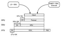
- FIG. 2 is a diagram showing an OTN frame structure.
- OTN frames have a hierarchical structure and are called OPU (Optical Channel Payload Unit) frames, ODU (Optical Channel Data Unit) frames, and OTU (Optical Channel Transport Unit) frames from the lower layer to the upper layer.
- OPU Optical Channel Payload Unit
- ODU Optical Channel Data Unit
- OTU Optical Channel Transport Unit
- the client signal such as SONET / SDH or Ethernet is accommodated in the payload, and an overhead (OH) as control information is added to the payload to generate an OPU frame.
- an ODU frame is generated by adding overhead to the OPU frame.
- an overhead and an error correction code FEC: Forward Error Correction
- FEC Forward Error Correction
- the overhead of the OPU frame is called OPU-OH
- the overhead of the ODU frame is called ODU-OH
- the overhead of the OTU frame is called OTU-OH.
- the client signal accommodated in the payload can accommodate a LO-ODU frame in addition to a data signal such as SONET / SDH or Ethernet.
- FIG. 3 shows an OTU frame format.
- the OTU frame includes an overhead area, a payload area, and an FEC area.
- the overhead area has a frame size of 16 bytes ⁇ 4 rows in the first to 16th columns
- the payload area has a frame size of 3808 bytes ⁇ 4 rows in the 17th to 3824 columns
- the FEC area Has a frame size of 256 bytes ⁇ 4 rows in the 3825th column to the 4080th column.
- the overhead area includes OPU-OH, which is the overhead of the OPU frame, ODU-OH, which is the overhead of the ODU frame, and OTU-OH, which is the overhead of the OTU frame. Further, FAS (Frame Alignment Signal) which is a frame head signal indicating the head of the frame is included.
- the FAS is arranged in the 1st to 6th columns of the 1st row.
- the OTU-OH is arranged in the 7th to 14th columns of the first row, and the ODU-OH is arranged in the 1st to 14th columns of the 2nd to 4th rows. Further, the OPU-OH is arranged in the 15th to 16th columns of the 1st to 4th rows.
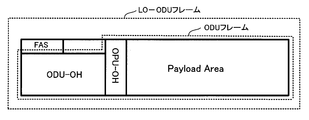
- Fig. 4 shows the frame format of LO-ODU.
- the LO-ODU has a frame format in which an FAS is added to an ODU frame, and the overhead area includes FAS, ODU-OH, and OPU-OH.
- the frame format of HO-ODU to which LO-ODU is mapped is the same format as the ODU frame (the overhead area of HO-ODU includes ODU-OH and OPU-OH).
- mapping the mapping method of LO-ODU to HO-ODU will be explained.
- the HO-ODU payload area is first divided into a plurality of slots, and the LO-ODU is mapped to the divided slots corresponding to the required bandwidth of the LO-ODU.
- the divided slots are referred to as TS (Tributary Slot).
- HO-ODU corresponds to an upper layer frame
- LO-ODU corresponds to a lower layer frame.
- Fig. 5 is a diagram showing HO-ODU payload division.
- a payload division structure in HO-ODU4 is shown.
- the payload area is divided by TS whose band is equivalent to about 1.25 Gbs, and 80 TSs are divided as one unit.
- LO-ODU is mapped to 80 TS units.
- 80 TSs are grouped as one unit from the left to the right and numbered # 1 to # 80.
- each TS has a bandwidth equivalent to about 1.25 Gbs
- LO-ODU0 of about 1.25 Gbs
- LO-ODU0 is mapped to one TS out of 80 TSs.
- the transmission rate is about 2.5 Gbs LO-ODU1
- the LO-ODU1 is mapped to two TSs out of the 80 TSs.
- the transmission rate is LO-ODU2 of about 10 Gbs
- LO-ODU2 is mapped to 8 TSs out of 80 TSs.
- the transmission rate is about 40 Gbs LO-ODU3
- LO-ODU3 is mapped to 32 TSs out of 80 TSs.
- FIGS. 6 and 7 are diagrams showing mapping states of LO-ODU0.
- FIG. 6 shows a state where LO-ODU0 is mapped to the payload of HO-ODU4.
- FIG. 7 shows a mapping state of LO-ODU0 when TS # 1 to TS # 80 are arranged in the vertical direction.
- FIG. 8 and 9 are diagrams showing the mapping state of LO-ODU1.
- FIG. 8 shows a state where LO-ODU1 is mapped to the payload of HO-ODU4. Since LO-ODU1 has a transmission rate of about 2.5 Gbs, it is mapped to two TSs. In the figure, it is an example of mapping to TS # 2 and TS # 5 (TS # 2). TS # 5 becomes an allocation slot).
- FIG. 9 shows a mapping state of LO-ODU1 when TS # 1 to TS # 80 are arranged in the vertical direction.
- FIG. 10 shows the case of LO-ODU1.
- LO-ODU1 when TS # 2 and TS # 5 are used as two TSs, the mapping of data at this time has a flow as indicated by arrows in the figure. That is, mapping is performed across two TSs.
- Fig. 11 shows the case of LO-ODU2.
- LO-ODU2 when TS # 4, # 7, # 10, # 13, # 16, # 19, # 22, and # 25 are used as 8 TSs, the data mapping at this time is 8 TSs. Are mapped in the flow as shown by the arrows in the figure.
- FIG. 12 is a diagram illustrating a state in which a staff is inserted. If there is a difference between the band secured by the HO-ODU TS and the LO-ODU band, as shown in the figure, insert the fixed pattern stuff data as appropriate, and perform mapping while performing stuffing. Do. In this way, LO-ODUs are discretely arranged with respect to HO-ODUs and discontinuously with the stuff region interposed therebetween.
- FIG. 13 is a diagram illustrating a configuration example of a frame receiving apparatus.
- the frame receiving apparatus 10a is assumed to perform HO-ODU4 frame reception processing, and shows a configuration example in the case of processing 80 TSs.
- the frame receiving apparatus 10a includes an HO-ODU overhead processing unit 11a, a TS division processing unit 11b, a demapping processing unit 12a-1 to 12a-80, an FAS element detection unit 12b-1 to 12b-80, a frame synchronization processing unit 120, LO-ODU overhead extracting units 12d-1 to 12d-80, BIP (Bit Interleaved Parity) computing units 12e-1 to 12e-80, LO-ODU overhead processing unit 12f and BIP check processing unit 12g are provided.
- HO-ODU overhead processing unit 11a includes an HO-ODU overhead processing unit 11a, a TS division processing unit 11b, a demapping processing unit 12a-1 to 12a-80, an FAS element detection unit 12b-1 to 12b-80, a frame synchronization processing unit 120, LO-ODU overhead extracting units 12d-1 to 12d-80, BIP (Bit Interleaved Parity) computing units 12e-1 to 12e-80, LO-
- the HO-ODU overhead processing unit 11a and the TS division processing unit 11b are included in the function of the frame receiving unit 11 in FIG. 1, and the other components are included in the function of the frame synchronization detecting unit 12 in FIG.
- the HO-ODU overhead processing unit 11a receives the HO-ODU4 frame and recognizes the overhead. Then, the demapping information indicating the staff position and the connection information are recognized and output from the recognized overhead.
- connection information is information indicating the number of TSs among the plurality of divided TSs where the LO-ODU is mapped. Therefore, in this example, when LO-ODU is mapped to HO-ODU4 on the frame transmission side, it is information indicating which TS of 80 TSs is mapped to LO-ODU. .
- the connection information regarding LO-ODU0 is TS # 1.
- the connection information regarding LO-ODU0 is TS # 1.
- the concatenation information regarding LO-ODU1 is TS # 2 and TS # 5 (the concatenation information will also be described later in FIG. 14).
- the TS division processing unit 11b receives the HO-ODU4 frame and recognizes the payload. Then, the payload portion of the HO-ODU4 frame is divided into TS units, and data mapped to the TS is output.
- the demapping processing units 12a-1 to 12a-80 recognize the data portion and the stuff portion in one TS based on the demapping information.
- the FAS element detection units 12b-1 to 12b-80 detect the FAS elements forming the FAS from the data string for each TS, and generate FAS element flags.
- the frame synchronization processing unit 120 performs LO-ODU frame synchronization detection and frame recognition by operating an internal frame counter based on the connection information and the FAS element flag. In addition, control information including overhead position information of LO-ODU frames and range information of BIP calculation is output.
- the LO-ODU overhead extraction units 12d-1 to 12d-80 extract the LO-ODU overhead for each TS based on one overhead position information of the control information, and output the overhead data (TS separated data string). The overhead is extracted as it is). Based on the BIP calculation range information, the BIP calculation units 12e-1 to 12e-80 perform the BIP calculation for each TS and output the calculation result (the BIP calculation is performed with the TS separated data string).
- the LO-ODU overhead processing unit 12f collects overhead information extracted by the LO-ODU overhead extracting units 12d-1 to 12d-80 and performs monitoring processing (system connection information and operation management information included in the overhead). Etc.). Also, monitor result information including an alarm signal indicating failure information, a status signal indicating an operation state, and the like is output.
- the BIP check processing unit 12g aggregates the BIP calculation results calculated by the BIP calculation units 12e-1 to 12e-80 to obtain a BIP calculation value as an LO-ODU frame, and then performs a BIP check. Also, communication quality state information including an alarm signal indicating a communication error state, a status signal indicating a communication quality level, and the like is output as a BIP calculation result.
- FIG. 14 is a diagram for explaining the connection information. The determination of which TS and which TS are paired and the LO-ODU is mapped is determined by the concatenation information stored in the overhead in the HO-ODU.
- the logical port number for each TS is stored, and it is possible to identify which TS is connected from this information.
- TS # 2 and TS # 5 have the same value of “1”, so it can be seen that the two are connected.
- FIG. 15 is a diagram showing the FAS element flag.
- the FAS is 48 bytes, and has FAS elements of 0xF6 and 0x28 (hereinafter, “0x” is omitted).
- the FAS pattern is 48 bytes of F6, F6, F6, 28, 28, 28.
- the FAS element flag includes the F6 element flag and the 28 element flag.
- FIG. 16 is a diagram showing an example of the FAS element flag generation pattern.
- An example of a FAS element flag generation pattern related to LO-ODU0 is shown. Since LO-ODU0 maps a data string to one TS # 1, only one TS # 1 includes FAS elements of F6, F6, F6, 28, 28, 28 and 1 byte. Therefore, the F6 element flag fa is set for the F6 portion, and the 28 element flag fb is set for the 28 portion.
- FIG. 17 is a diagram showing an example of a FAS element flag generation pattern. The example of the generation pattern of the FAS element flag regarding LO-ODU1 is shown. LO-ODU1 maps a data string to two TS # 2 and TS # 5.
- the F6 element flags fa1 and fa2 are set for the F6 portion
- the 28 element flags fb1 and fb2 are set for the 28 portion.
- the operation for each component will be described by taking as an example the case where the LO-ODU1 signal is mapped to TS # 2 and TS # 5 in the HO-ODU4 frame.
- the LO-ODU1 signal is mapped to TS # 2 and TS # 5 of the HO-ODU4 frame and transmitted.
- the mapping state of LO-ODU1 to HO-ODU4 is as described above with reference to FIGS.
- FIG. 18 is a diagram showing the operation of the demapping process.
- LO-ODU1 is mapped while the rate is adjusted by the staff.
- the demapping processing unit sorts the data area and the stuff area based on the demapping information indicating the stuff position, and an enable signal indicating that the data area is an effective portion (for example, the H level in the data area, the stuff area At L level).
- FIG. 19 is a diagram showing the operation of FAS element detection.
- the FAS element detection unit detects FAS elements F6 and 28 from the TS # 2 and TS # 5 data streams in which the staff is inserted, and generates a FAS element flag.
- the detection of FAS elements and the generation of flags are the same as in FIG.
- FIG. 20 is a diagram illustrating a block configuration of the frame synchronization processing unit 120.
- the frame synchronization processing unit 120 includes TS individual frame synchronization processing units 120c-1 to 120c-80.
- the TS individual frame synchronization processing units 120c-1 to 120c-80 receive the FAS element flag (F6 element flag, 28 element flag) and connection information, and perform control information (overhead position information, BIP) by internal processing. (Calculation range information) is output.
- FIG. 21 is a diagram showing a block configuration of the TS individual frame synchronization processing unit.
- the TS individual frame synchronization processing unit 120c includes an FAS pattern detection unit 121c, a state transition processing unit 122c, and a frame counter 123c.
- the FAS pattern detection unit 121c detects the FAS appearance pattern (F6F6F6282828) based on the FAS element flag (F6 element flag, 28 element flag) and the connection information, and outputs the FAS detection information.
- the state transition processing unit 122c protects the synchronization based on the FAS detection information, and manages the state transition of the frame synchronization establishment state and the out of synchronization state. For example, when synchronization is established n times consecutively, it is recognized that frame synchronization is established, and when synchronization is not established n times consecutively, it is recognized as being out of synchronization. Then, a state notification signal indicating the recognition result of whether synchronization is established or out of synchronization is output.
- the frame counter 123c receives synchronization establishment information indicating whether or not frame synchronization is established from the state transition processing unit 122c, and operates a counter for recognizing the LO-ODU frame. From the value of the frame counter 123c, overhead position information and BIP calculation range information are generated and output.
- FIG. 22 is a diagram showing FAS detection information.
- the FAS pattern detection unit 121c has FAS detection flag and pattern ID (ID for identifying whether TS # 2 is detected at the head or TS # 5 is detected as the head) as FAS detection information. Is output to the state transition processing unit 122c.
- FIG. 23 is a diagram for explaining the operation of the frame counter.
- the state transition processing unit 122c performs synchronization detection with protection based on the FAS detection flag and the pattern ID included in the FAS detection information.
- a Load signal is output to the frame counter 123c.
- the frame counter 123c When the frame counter 123c receives the Load signal, it performs initialization for phase alignment and synchronizes the data and the counter. Then, the overhead position and BIP calculation range are specified, and the overhead position and BIP calculation range are output as control information.
- FIG. 24 is a diagram showing a TS individual overhead processing unit.
- the LO-ODU overhead processing unit 12f includes TS individual overhead processing units 12f-1 to 12f-80.
- the TS individual overhead processing units 12f-1 to 12f-80 collect the overhead information from each TS output from the LO-ODU overhead extraction units 12d-1 to 12d-80, perform monitoring processing, and display the monitoring results. Output.
- FIG. 25 is a diagram showing the TS individual BIP check processing unit.
- the BIP check processing unit 12g includes TS individual BIP check processing units 12g-1 to 12g-80.
- the TS individual BIP check processing units 12g-1 to 12g-80 collect the BIP calculation results from the TSs transmitted from the BIP calculation units 12e-1 to 12e-80 and aggregate them into one, and the LO- Processes as a BIP calculation result in ODU units, and outputs a BIP check result.
- the head position is detected without shaping the data string for each type of LO-ODU, Recognizes LO-ODU frames.
- overhead extraction and BIP processing are performed in the state of being divided into TSs, so cross-connecting is performed in units of TSs and multiplexed again without returning from the LO-ODU to the TS column again. Since this can be easily performed, the apparatus configuration can be simplified.
- the TS number 32
- the TS number 8
Landscapes
- Engineering & Computer Science (AREA)
- Computer Networks & Wireless Communication (AREA)
- Signal Processing (AREA)
- Physics & Mathematics (AREA)
- Optics & Photonics (AREA)
- Time-Division Multiplex Systems (AREA)
Abstract
フレーム同期検出を効率よく行って装置規模の削減を図る。 フレーム送信部は、上位レイヤフレームのペイロード領域を複数のスロットに分割して、スロットに下位レイヤフレームをマッピングし、複数のスロットの内のどのスロットに、同一種別の下位レイヤフレームがマッピングされているかを示す連接情報を含めて上位レイヤフレームを送信する。フレーム同期検出部は、連接情報にもとづいて、同一種別の下位レイヤフレームがマッピングされているスロットである割当スロットを認識し、割当スロットにマッピングされている、同一種別の下位レイヤフレームのフレーム先頭信号を認識して、フレーム同期を検出する。
Description
本発明は、情報通信を行う通信システム、フレーム同期検出を行うフレーム同期検出装置およびフレーム同期検出方法に関する。
光通信の基幹網を支える伝送技術の1つに、OTN(Optical Transport Network)があり、ITU-T(International Telecommunication Union Telecommunication Standardization Sector)で標準化されている。
OTNは、SONET/SDH(Synchronous Optical Network/Synchronous Digital Hierarchy)、Ethernet(登録商標)等のクライアント信号を収容し、階梯構造を持つフレームを生成して、WDM(Wavelength Division Multiplexing)に適したデータ伝送を行う技術である。
一方、近年になって、既存の階梯構造との接続性を維持しながら、多様なクライアント信号をいかに収容して、効率よくデータ伝送を実現するかのOTN拡張の議論が高まっている。
OTN拡張の一例としては、LO(Lower Order)-ODU(Optical Channel Data Unit)、HO(High Order)-ODUのクライアント収容方式が注目されている。
これは、クライアント信号として、SONET/SDHやEthernet等のデータ信号の他に、フレーム構造を持つ信号も多重化して収容させることで、クライアント信号収容の柔軟性を高めようとするものである。
これは、クライアント信号として、SONET/SDHやEthernet等のデータ信号の他に、フレーム構造を持つ信号も多重化して収容させることで、クライアント信号収容の柔軟性を高めようとするものである。
クライアント信号として収容されるフレームがLO-ODUと呼ばれ、LO-ODUの格納先のフレームがHO-ODUと呼ばれる。LO-ODUは、HO-ODUのペイロード領域内にマッピングされて送信され、受信側において、LO-ODUのフレーム同期が検出されてモニタリングが行われる。
フレーム同期に関する従来技術としては、STM-N内のSTM1の個々についてフレーム同期をとる技術が提案されている(特許文献1)。また、フレーム同期用の固定パターンの検出を短縮化した技術が提案されている(特許文献2)。
HO-ODUに収容されるLO-ODUは、伝送レートによって複数の種別があり、HO-ODUにマッピングされる際は、複数種別のLO-ODUが1つのHO-ODUのペイロード領域に離散的にマッピングされる。また、受信側でLO-ODUをモニタリングするときは、LO-ODUのフレーム同期を確立する。
フレーム同期を確立するにあたっては、LO-ODU種別毎のセレクタ回路を設けて各種別のLO-ODUを選別し、選別後のLO-ODUに対して、同期検出制御を行うといった構成が考えられる。
しかし、このような回路構成では、LO-ODUの種別毎にフレーム同期検出を行うための並列した複数の制御系が必要になる。このため、想定しうるLO-ODU最大種別の個数分の制御系をあらかじめ用意しておくことになり、装置規模(回路規模)が増大し、またインプリメントの難易度が増大するといった問題があった。
本発明はこのような点に鑑みてなされたものであり、フレーム同期検出を効率よく行って装置規模の削減を図った通信システムを提供することを目的とする。
また、本発明の他の目的は、フレーム同期検出を効率よく行って装置規模の削減を図ったフレーム同期検出装置を提供することである。
また、本発明の他の目的は、フレーム同期検出を効率よく行って装置規模の削減を図ったフレーム同期検出装置を提供することである。
さらに、本発明の他の目的は、フレーム同期検出を効率よく行って装置規模の削減を図ったフレーム同期検出方法を提供することである。
上記課題を解決するために、通信システムが提供される。この通信システムは、上位レイヤフレームのペイロード領域を複数のスロットに分割して、前記スロットに下位レイヤフレームをマッピングし、複数の前記スロットの内のどの前記スロットに、同一種別の前記下位レイヤフレームがマッピングされているかを示す連接情報を含めて前記上位レイヤフレームを送信するフレーム送信部を含むフレーム送信装置と、前記上位レイヤフレームを受信するフレーム受信部と、前記下位レイヤフレームのフレーム同期を検出するフレーム同期検出部とを含むフレーム受信装置とを備える。前記フレーム同期検出部は、前記連接情報にもとづいて、同一種別の前記下位レイヤフレームがマッピングされている前記スロットである割当スロットを認識し、前記割当スロットにマッピングされている、同一種別の前記下位レイヤフレームのフレーム先頭信号を認識して、前記フレーム同期を検出する。
装置規模を削減することが可能になる。
本発明の上記および他の目的、特徴および利点は本発明の例として好ましい実施の形態を表す添付の図面と関連した以下の説明により明らかになるであろう。
本発明の上記および他の目的、特徴および利点は本発明の例として好ましい実施の形態を表す添付の図面と関連した以下の説明により明らかになるであろう。
以下、本発明の実施の形態を図面を参照して説明する。図1は通信システムの構成例を示す図である。通信システム1は、フレーム送信装置20とフレーム受信装置10を備える。
フレーム送信装置20は、フレーム送信部21を含む。フレーム送信部21は、上位レイヤフレームのペイロード領域を複数のスロットに分割して、分割したスロットに下位レイヤフレームをマッピングする。
また、複数のスロットの内のどのスロットに、同一種別の下位レイヤフレームがマッピングされているかを示す連接情報を生成する。そして、上位レイヤフレームのオーバヘッドに連接情報を含めて、上位レイヤフレームを送信する。
フレーム受信装置10は、フレーム受信部11とフレーム同期検出部12を含む。フレーム受信部11は、上位レイヤフレームを受信する。フレーム同期検出部12は、上位レイヤフレームにマッピングされている下位レイヤフレームのフレーム同期を検出する。
ここで、フレーム同期検出部12は、連接情報にもとづいて、同一種別の下位レイヤフレームがマッピングされているスロットである割当スロットを認識する。そして、割当スロットにマッピングされている、同一種別の下位レイヤフレームのフレーム先頭信号を認識して、フレーム同期を検出する。
この場合、フレーム同期検出部12では、スロットにマッピングされている、下位レイヤフレームのフレーム先頭信号を形成しているフレーム先頭信号要素をすべて検出して、すべてのフレーム先頭信号要素のフラグを生成する。
その後、割当スロットにマッピングされているフレーム先頭信号要素のフラグを集約することで、同一種別の下位レイヤフレームのフレーム先頭信号を認識して、下位レイヤフレームのフレーム同期検出を行う。なお、詳細動作については具体例を用いて後述する。
次に通信システム1をOTNのシステムに適用した場合について以降説明する。最初にOTNのフレーム構成について説明する。
図2はOTNのフレーム階梯構造を示す図である。OTNのフレームは、階梯構造をとり、下位レイヤから上位レイヤに向かって、OPU(Optical Channel Payload Unit)フレーム、ODU(Optical Channel Data Unit)フレーム、OTU(Optical Channel Transport Unit)フレームと呼ばれる。
図2はOTNのフレーム階梯構造を示す図である。OTNのフレームは、階梯構造をとり、下位レイヤから上位レイヤに向かって、OPU(Optical Channel Payload Unit)フレーム、ODU(Optical Channel Data Unit)フレーム、OTU(Optical Channel Transport Unit)フレームと呼ばれる。
SONET/SDH、Ethernet等のクライアント信号をペイロードに収容し、このペイロードに制御情報であるオーバヘッド(OH)を付加してOPUフレームが生成される。また、OPUフレームにオーバヘッドを付加してODUフレームが生成される。さらに、ODUフレームにオーバヘッドと誤り訂正符号(FEC:Forward Error Correction)を付加してOTUフレームが生成される。
なお、OPUフレームのオーバヘッドはOPU-OHと呼ばれ、ODUフレームのオーバヘッドはODU-OHと呼ばれ、OTUフレームのオーバヘッドはOTU-OHと呼ばれる。また、ペイロードに収容されるクライアント信号には、SONET/SDH、Ethernet等のデータ信号の他に、LO-ODUのフレームが収容可能である。
図3はOTUのフレームフォーマットを示す図である。OTUフレームは、オーバヘッド領域、ペイロード領域およびFEC領域を備える。
オーバヘッド領域は、1列目~16列目の16バイト×4行のフレームサイズを有し、ペイロード領域は、17列目~3824列目の3808バイト×4行のフレームサイズを有し、FEC領域は、3825列目~4080列目の256バイト×4行のフレームサイズを有する。
オーバヘッド領域は、1列目~16列目の16バイト×4行のフレームサイズを有し、ペイロード領域は、17列目~3824列目の3808バイト×4行のフレームサイズを有し、FEC領域は、3825列目~4080列目の256バイト×4行のフレームサイズを有する。
オーバヘッド領域には、OPUフレームのオーバヘッドであるOPU-OHと、ODUフレームのオーバヘッドであるODU-OHと、OTUフレームのオーバヘッドであるOTU-OHとが含まれる。さらに、フレームの先頭を示すフレーム先頭信号であるFAS(Frame Alignment Signal)が含まれる。
FASは、1行目の1列目~6列目に配置される。また、OTU-OHは、1行目の7列目~14列目に配置され、ODU-OHは、2行目~4行目の1列目~14列目に配置される。さらに、OPU-OHは、1行目~4行目の15列目~16列目に配置される。
図4はLO-ODUのフレームフォーマットを示す図である。LO-ODUは、ODUフレームにFASが付加されたフレームフォーマットを有しており、オーバヘッド領域には、FAS、ODU-OHおよびOPU-OHが含まれる。
なお、LO-ODUがマッピングされるHO-ODUのフレームフォーマットは、ODUフレームと同じフォーマットである(HO-ODUのオーバヘッド領域には、ODU-OHおよびOPU-OHが含まれる)。
次にHO-ODUへのLO-ODUのマッピング方法について説明する。マッピングを行うにあたっては、まずHO-ODUのペイロード領域を複数のスロットに分割し、LO-ODUの必要帯域分の分割スロットに対して、LO-ODUをマッピングする。以降では、分割されたスロットをTS(Tributary Slot)と呼ぶ。なお、HO-ODUは、上位レイヤフレームに該当し、LO-ODUは、下位レイヤフレームに該当する。
図5はHO-ODUのペイロード分割を示す図である。一例として、HO-ODU4におけるペイロードの分割構成を示している。HO-ODU4では、帯域が約1.25Gbs相当のTSでペイロード領域を分割して、TS80個を1つの単位として区分けする。そして、1単位80個のTSにLO-ODUをマッピングする。図では左から右方向へTS80個を1つのまとまりとして、#1~#80の番号を付けている。
ここで、TS1つ当たり約1.25Gbs相当の帯域を持つため、伝送レートが約1.25GbsのLO-ODU0であれば、80個のTSの内の1個のTSにLO-ODU0をマッピングすることになる。
また、伝送レートが約2.5GbsのLO-ODU1であれば、80個のTSの内の2個のTSにLO-ODU1をマッピングする。さらに、伝送レートが約10GbsのLO-ODU2であれば、80個のTSの内の8個のTSにLO-ODU2をマッピングする。さらにまた、伝送レートが約40GbsのLO-ODU3であれば、80個のTSの内の32個のTSにLO-ODU3をマッピングすることになる。
また、伝送レートが約2.5GbsのLO-ODU1であれば、80個のTSの内の2個のTSにLO-ODU1をマッピングする。さらに、伝送レートが約10GbsのLO-ODU2であれば、80個のTSの内の8個のTSにLO-ODU2をマッピングする。さらにまた、伝送レートが約40GbsのLO-ODU3であれば、80個のTSの内の32個のTSにLO-ODU3をマッピングすることになる。
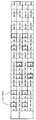
次にLO-ODU0およびLO-ODU1におけるマッピング例について図6~図9を用いて説明する。図6、図7はLO-ODU0のマッピング状態を示す図である。図6は、HO-ODU4のペイロードにLO-ODU0をマッピングしている状態を示している。
LO-ODU0は、伝送レートが約1.25Gbsであるので、1個のTSにマッピングすることになり、図の場合は、TS#1にマッピングしている例である(TS#1が割当スロットとなる)。また、図7は、TS#1~TS#80を縦方向に並べたときのLO-ODU0のマッピング状態を示している。
図8、図9はLO-ODU1のマッピング状態を示す図である。図8はHO-ODU4のペイロードにLO-ODU1をマッピングしている状態を示している。LO-ODU1は、伝送レートが約2.5Gbsであるので、2個のTSにマッピングすることになり、図の場合は、TS#2、TS#5にマッピングしている例である(TS#2、TS#5が割当スロットとなる)。また、図9は、TS#1~TS#80を縦方向に並べたときのLO-ODU1のマッピング状態を示している。
複数のTSを使用してマッピングする場合においては、上記のように隣接するTSを使う必要はなく、任意のTSを使用することが可能である。なお、LO-ODU3以降のLO-ODUkについても上記と同様なやり方でマッピングされる。
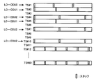
次に複数のTSにLO-ODUをマッピングする際の順番について説明する。図10、図11はマッピングの順番を示す図である。図中に示す番号は、マッピングの順番を示している。図10はLO-ODU1の場合を示している。LO-ODU1では、2つのTSとして、TS#2、TS#5を使用する場合、このときのデータのマッピングは、図に示す矢印のような流れとなる。すなわち、2つのTSにまたがってマッピングされる。
図11はLO-ODU2の場合を示している。LO-ODU2では、8つのTSとして、TS#4、#7、#10、#13、#16、#19、#22、#25を使用する場合、このときのデータのマッピングは、8つのTSにまたがって図に示す矢印のような流れでマッピングされる。
次にスタッフィングについて説明する。図12はスタッフが挿入されている状態を示す図である。HO-ODUのTSで確保された帯域と、LO-ODUの帯域とに差分がある場合は、図に示すように、固定パターンのスタッフデータを適宜挿入して、スタッフィングを行いながら飛び飛びにマッピングを行う。このように、HO-ODUに対して、LO-ODUは離散的に、かつスタッフ領域を挟みながら不連続に配置されることになる。
次にフレーム受信装置10(フレーム同期検出装置)の構成について説明する。図13はフレーム受信装置の構成例を示す図である。フレーム受信装置10aは、HO-ODU4フレームの受信処理を行うものとし、80個のTSを処理する場合の構成例を示している。
フレーム受信装置10aは、HO-ODUオーバヘッド処理部11a、TS分割処理部11b、デマッピング処理部12a-1~12a-80、FAS要素検出部12b-1~12b-80、フレーム同期処理部120、LO-ODUオーバヘッド抽出部12d-1~12d-80、BIP(Bit Interleaved Parity)演算部12e-1~12e-80、LO-ODUオーバヘッド処理部12fおよびBIPチェック処理部12gを備える。
なお、HO-ODUオーバヘッド処理部11aとTS分割処理部11bは、図1のフレーム受信部11の機能に含まれ、その他の構成要素は、図1のフレーム同期検出部12の機能に含まれる。
HO-ODUオーバヘッド処理部11aは、HO-ODU4フレームを受信してオーバヘッドを認識する。そして、認識したオーバヘッドから、スタッフ位置を示すデマッピング情報と、連接情報とを認識して出力する。
なお、連接情報は、分割された複数TSの内の何番のTSにLO-ODUがマッピングされているかを示す情報である。したがって、ここの例では、フレーム送信側でHO-ODU4にLO-ODUがマッピングされた際に、80個のTSの内の何番のTSにLO-ODUがマッピングされているかを示す情報となる。
例えば、LO-ODU0がTS#1にマッピングされているならば、LO-ODU0に関する連接情報は、TS#1となる。また、LO-ODU1がTS#2、TS#5にマッピングされているならば、LO-ODU1に関する連接情報は、TS#2、TS#5となる(連接情報については図14でも後述する)。
TS分割処理部11bは、HO-ODU4フレームを受信してペイロードを認識する。そして、HO-ODU4フレームのペイロード部分をTS単位に分割し、TSにマッピングされているデータを出力する。
デマッピング処理部12a-1~12a-80は、デマッピング情報にもとづいて、1つのTS内のデータ部分とスタッフ部分とを認識する。FAS要素検出部12b-1~12b-80は、TS毎のデータ列より、FASを形成しているFAS要素を検出して、FAS要素フラグを生成する。
フレーム同期処理部120は、連接情報およびFAS要素フラグにもとづき、内部に有するフレームカウンタを動作させることによって、LO-ODUのフレーム同期検出およびフレーム認識を行う。また、LO-ODUフレームのオーバヘッドの位置情報やBIP演算の範囲情報を含む制御情報を出力する。
LO-ODUオーバヘッド抽出部12d-1~12d-80は、制御情報の1つのオーバヘッド位置情報にもとづき、TS毎にLO-ODUのオーバヘッドを抽出してオーバヘッドのデータを出力する(TS分離したデータ列のままオーバヘッド抽出を行う)。BIP演算部12e-1~12e-80は、BIP演算の範囲情報にもとづいて、TS毎にBIP演算を行い、演算結果を出力する(TS分離したデータ列のままBIP演算を行う。
LO-ODUオーバヘッド処理部12fは、LO-ODUオーバヘッド抽出部12d-1~12d-80で抽出されたオーバヘッドの情報を集約してモニタ処理を行う(オーバヘッドに含まれるシステムの接続情報、運用管理情報等のモニタを行う)。また、障害情報を示すアラーム信号や、運用状態を示すステータス信号等を含むモニタ結果情報を出力する。
BIPチェック処理部12gは、BIP演算部12e-1~12e-80にて演算されたBIP演算結果を集約して、LO-ODUフレームとしてのBIP演算値とした後、BIPチェックを行う。また、BIP演算結果として通信誤り状態を示すアラーム信号や、通信品質レベルを示すステータス信号等を含む通信品質状態情報を出力する。
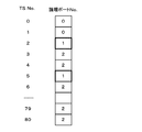
図14は連接情報を説明するための図である。どのTSとどのTSとが組みになって、LO-ODUがマッピングされているかという判断は、HO-ODU内のオーバヘッドに格納されている連接情報により判断する。
連接情報の入ったオーバヘッドは、各TSに対する論理ポート番号が格納されており、この情報からどのTS同士が連接しているかが識別可能となる。図の例では、TS#2、TS#5のみが“1”という同じ値になっているため、この2つが連接しているとわかる。
次にFAS要素検出部12b-1~12b-80が出力するFAS要素フラグについて説明する。図15はFAS要素フラグを示す図である。例えば、FASは48byteであり、0xF6、0x28のFAS要素を持つものとする(以下、“0x”の表記は省略する)。FASのパターンは、F6、F6、F6、28、28、28の48byteである。また、FASは、F6要素と28要素を含むため、FAS要素フラグは、F6要素フラグと28要素フラグを有している。
図16はFAS要素フラグの生成パターン例を示す図である。LO-ODU0に関するFAS要素フラグの生成パターン例を示している。LO-ODU0は、1つのTS#1にデータ列をマッピングするので、TS#1のみにF6、F6、F6、28、28、28と1byteずつFAS要素が配置される。したがって、F6の部分に対してF6要素フラグfaが立ち、28の部分に対して28要素フラグfbが立つ。
図17はFAS要素フラグの生成パターン例を示す図である。LO-ODU1に関するFAS要素フラグの生成パターン例を示している。LO-ODU1は、2つのTS#2、TS#5にデータ列をマッピングする。
したがって、図10で上述したように、FAS要素の1つ目のF6がTS#2に配置すると、TS#5にFAS要素の2つ目のF6が配置し、TS#2にFAS要素の3つ目のF6が配置する。また、TS#5にFAS要素の1つ目の28が配置し、TS#2にFAS要素の2つ目の28が配置し、TS#5にFAS要素の3つ目の28が配置する。したがって、F6の部分に対してF6要素フラグfa1、fa2が立ち、28の部分に対して28要素フラグfb1、fb2が立つ。
次に構成要素毎の動作について、HO-ODU4フレームにおけるTS#2、TS#5にLO-ODU1の信号がマッピングされている場合を例にして説明する。
フレーム送信側では、HO-ODU4フレームのTS#2、TS#5にLO-ODU1の信号をマッピングして送信する。HO-ODU4へのLO-ODU1のマッピング状態は図8、図9で上述した通りである。
フレーム送信側では、HO-ODU4フレームのTS#2、TS#5にLO-ODU1の信号をマッピングして送信する。HO-ODU4へのLO-ODU1のマッピング状態は図8、図9で上述した通りである。
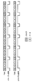
図18はデマッピング処理の動作を示す図である。LO-ODU1は、スタッフによりレート調整されながらマッピングされている。デマッピング処理部では、スタッフ位置を示すデマッピング情報にもとづいて、データ領域とスタッフ領域とを選別し、データ領域が有効部分であることを示すイネーブル信号(例えば、データ領域でHレベル、スタッフ領域でLレベル)を生成する。
図19はFAS要素検出の動作を示す図である。FAS要素検出部は、スタッフが挿入されているTS#2、TS#5の各データストリームから、F6、28のFAS要素を検出してFAS要素フラグを生成する。なお、FAS要素の検出、フラグ生成については、図17と同じなので説明は省略する。
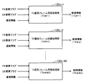
図20はフレーム同期処理部120のブロック構成を示す図である。フレーム同期処理部120は、TS個別フレーム同期処理部120c-1~120c-80を含む。TS個別フレーム同期処理部120c-1~120c-80は、FASの要素フラグ(F6要素フラグ、28要素フラグ)と連接情報とを受信して、内部の処理によって、制御情報(オーバヘッド位置情報、BIP演算範囲情報)を出力する。
図21はTS個別フレーム同期処理部のブロック構成を示す図である。TS個別フレーム同期処理部120cは、FASパターン検出部121c、状態遷移処理部122cおよびフレームカウンタ123cを含む。
FASパターン検出部121cは、FAS要素フラグ(F6要素フラグ、28要素フラグ)と、連接情報とにもとづいて、FASの出現パターン(F6F6F6282828)を検出して、FAS検出情報を出力する。
状態遷移処理部122cは、FAS検出情報により同期保護をとり、フレーム同期確立状態および同期はずれ状態の状態遷移を管理する。例えば、n回連続して同期がとれた場合は、フレーム同期が確立している状態と認識し、n回連続して同期がとれない場合は、同期はずれ状態と認識する。そして、同期確立か同期はずれかの認識結果を示す状態通知信号を出力する。
フレームカウンタ123cは、状態遷移処理部122cより、フレーム同期が確立しているか否かを示す同期確立情報を受け取り、LO-ODUフレームを認識するためのカウンタを動作させる。フレームカウンタ123cの値より、オーバヘッドの位置情報やBIPの演算範囲情報を生成して出力する。
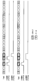
図22はFAS検出情報を示す図である。FASパターン検出部121cは、FASを検出した場合に、FAS検出情報としてFAS検出フラグとパターンID(TS#2を先頭として検出したのか、TS#5を先頭として検出したのかを識別するID)とを生成して、状態遷移処理部122cへ出力する。
図23はフレームカウンタの動作を説明するための図である。状態遷移処理部122cでは、FAS検出情報に含まれるFAS検出フラグおよびパターンIDにもとづいて、保護をとって同期検出を行う。同期確立した場合は、フレームカウンタ123cにLoad信号を出力する。
フレームカウンタ123cは、Load信号を受け取ると、位相合わせのための初期化を行い、データとカウンタの同期化を行う。そして、オーバヘッド位置やBIPの演算範囲を特定し、制御情報として、オーバヘッド位置およびBIP演算範囲を出力する。
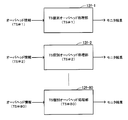
図24はTS個別オーバヘッド処理部を示す図である。LO-ODUオーバヘッド処理部12fは、TS個別オーバヘッド処理部12f-1~12f-80を含む。TS個別オーバヘッド処理部12f-1~12f-80は、LO-ODUオーバヘッド抽出部12d-1~12d-80から出力された、各TSからのオーバヘッド情報を収集してモニタ処理を行い、モニタ結果の出力を行う。
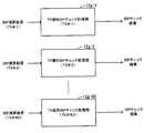
図25はTS個別BIPチェック処理部を示す図である。BIPチェック処理部12gは、TS個別BIPチェック処理部12g-1~12g-80を含む。TS個別BIPチェック処理部12g-1~12g-80は、BIP演算部12e-1~12e-80から送信された、各TSからのBIP演算結果を収集して1つに集約させて、LO-ODU単位のBIP演算結果として処理を行い、BIPチェック結果の出力を行う。
以上説明したように、本発明により、HO-ODUフレームに離散的にマッピングされたLO-ODUフレームに対して、LO-ODUを種別毎にデータ列を整形することなく先頭位置検出を行って、LO-ODUフレームを認識する。
このため、LO-ODUの種別毎にフレーム同期検出を行うための並列した複数の制御系の回路構成を持つ必要がなく、任意のLO-ODUの種別に対してフレーム同期検出を効率よく行うことができるので、装置規模の削減が可能になる。
また、各TSに分割したままの状態でオーバヘッドの抽出やBIP処理を実行しているので、LO-ODUから再びTSの列に戻すことなく、TS単位でクロスコネクトを行ったり、再び多重化したりすることが容易に行うことができるため、装置構成が簡素化できる。
なお、上記では、一例として、HO-ODU4のTS数=80に対して、LO-ODUがマッピングされている状態でのフレーム同期検出制御に関して説明したが、HO-ODU4に限定するものではない。例えば、HO-ODU3の場合はTS数=32となり、HO-ODU2の場合はTS数=8となり、HO-ODU1の場合はTS数=2となるが、基本装置構成は同様となる。
上記については単に本発明の原理を示すものである。さらに、多数の変形、変更が当業者にとって可能であり、本発明は上記に示し、説明した正確な構成および応用例に限定されるものではなく、対応するすべての変形例および均等物は、添付の請求項およびその均等物による本発明の範囲とみなされる。
1 通信システム
10 フレーム受信装置
11 フレーム受信部
12 フレーム同期検出部
20 フレーム送信装置
21 フレーム送信部
10 フレーム受信装置
11 フレーム受信部
12 フレーム同期検出部
20 フレーム送信装置
21 フレーム送信部
Claims (6)
- 上位レイヤフレームのペイロード領域を複数のスロットに分割して、前記スロットに下位レイヤフレームをマッピングし、複数の前記スロットの内のどの前記スロットに、同一種別の前記下位レイヤフレームがマッピングされているかを示す連接情報を含めて前記上位レイヤフレームを送信するフレーム送信部を含むフレーム送信装置と、
前記上位レイヤフレームを受信するフレーム受信部と、前記下位レイヤフレームのフレーム同期を検出するフレーム同期検出部とを含むフレーム受信装置と、
を備え、
前記フレーム同期検出部は、
前記連接情報にもとづいて、同一種別の前記下位レイヤフレームがマッピングされている前記スロットである割当スロットを認識し、
前記割当スロットにマッピングされている、同一種別の前記下位レイヤフレームのフレーム先頭信号を認識して、前記フレーム同期を検出する、
ことを特徴とする通信システム。 - 前記フレーム同期検出部は、
前記フレーム先頭信号を形成するフレーム先頭信号要素を検出してフラグを生成し、
前記割当スロットにマッピングされている前記フレーム先頭信号要素の前記フラグを集約して、同一種別の前記下位レイヤフレームの前記フレーム先頭信号を認識する、
ことを特徴とする請求の範囲第1項記載の通信システム。 - 上位レイヤフレームのペイロード領域が複数のスロットに分割されて、前記スロットに下位レイヤフレームがマッピングされた前記上位レイヤフレームを受信するフレーム受信部と、
前記下位レイヤフレームのフレーム同期を検出するフレーム同期検出部と、
を備え、
前記フレーム受信部は、複数の前記スロットの内のどの前記スロットに、同一種別の前記下位レイヤフレームがマッピングされているかを示す連接情報を抽出し、
前記フレーム同期検出部は、
前記連接情報にもとづいて、同一種別の前記下位レイヤフレームがマッピングされている前記スロットである割当スロットを認識し、
前記割当スロットにマッピングされている、同一種別の前記下位レイヤフレームのフレーム先頭信号を認識して、前記フレーム同期を検出する、
ことを特徴とするフレーム同期検出装置。 - 前記フレーム同期検出部は、
前記フレーム先頭信号を形成するフレーム先頭信号要素を検出してフラグを生成し、
前記割当スロットにマッピングされている前記フレーム先頭信号要素の前記フラグを集約して、同一種別の前記下位レイヤフレームの前記フレーム先頭信号を認識する、
ことを特徴とする請求の範囲第3項記載のフレーム同期検出装置。 - フレーム同期検出方法において、
上位レイヤフレームのペイロード領域が複数のスロットに分割されて、前記スロットに下位レイヤフレームがマッピングされた前記上位レイヤフレームを受信し、
複数の前記スロットの内のどの前記スロットに、同一種別の前記下位レイヤフレームがマッピングされているかを示す連接情報を抽出し、
前記連接情報にもとづいて、同一種別の前記下位レイヤフレームがマッピングされている前記スロットである割当スロットを認識し、
前記割当スロットにマッピングされている、同一種別の前記下位レイヤフレームのフレーム先頭信号を認識して、フレーム同期を検出する、
ことを特徴とするフレーム同期検出方法。 - 前記フレーム先頭信号を形成するフレーム先頭信号要素を検出してフラグを生成し、
前記割当スロットにマッピングされている前記フレーム先頭信号要素の前記フラグを集約して、同一種別の前記下位レイヤフレームの前記フレーム先頭信号を認識する、
ことを特徴とする請求の範囲第5項記載のフレーム同期検出方法。
Priority Applications (3)
| Application Number | Priority Date | Filing Date | Title |
|---|---|---|---|
| JP2012518170A JP5382217B2 (ja) | 2010-06-01 | 2010-06-01 | 通信システム、フレーム同期検出装置およびフレーム同期検出方法 |
| PCT/JP2010/059254 WO2011151892A1 (ja) | 2010-06-01 | 2010-06-01 | 通信システム、フレーム同期検出装置およびフレーム同期検出方法 |
| US13/672,053 US9203603B2 (en) | 2010-06-01 | 2012-11-08 | Communication system, frame synchronization detection apparatus, and frame synchronization detection method |
Applications Claiming Priority (1)
| Application Number | Priority Date | Filing Date | Title |
|---|---|---|---|
| PCT/JP2010/059254 WO2011151892A1 (ja) | 2010-06-01 | 2010-06-01 | 通信システム、フレーム同期検出装置およびフレーム同期検出方法 |
Related Child Applications (1)
| Application Number | Title | Priority Date | Filing Date |
|---|---|---|---|
| US13/672,053 Continuation US9203603B2 (en) | 2010-06-01 | 2012-11-08 | Communication system, frame synchronization detection apparatus, and frame synchronization detection method |
Publications (1)
| Publication Number | Publication Date |
|---|---|
| WO2011151892A1 true WO2011151892A1 (ja) | 2011-12-08 |
Family
ID=45066289
Family Applications (1)
| Application Number | Title | Priority Date | Filing Date |
|---|---|---|---|
| PCT/JP2010/059254 Ceased WO2011151892A1 (ja) | 2010-06-01 | 2010-06-01 | 通信システム、フレーム同期検出装置およびフレーム同期検出方法 |
Country Status (3)
| Country | Link |
|---|---|
| US (1) | US9203603B2 (ja) |
| JP (1) | JP5382217B2 (ja) |
| WO (1) | WO2011151892A1 (ja) |
Cited By (3)
| Publication number | Priority date | Publication date | Assignee | Title |
|---|---|---|---|---|
| JP2013207764A (ja) * | 2012-03-29 | 2013-10-07 | Fujitsu Ltd | データ伝送装置及びデータ伝送方法 |
| JP2014039108A (ja) * | 2012-08-13 | 2014-02-27 | Nippon Telegr & Teleph Corp <Ntt> | マルチレーン伝送方法およびそれを適用した装置 |
| JP2015167287A (ja) * | 2014-03-03 | 2015-09-24 | 富士通株式会社 | 光受信装置、及び光受信方法 |
Families Citing this family (3)
| Publication number | Priority date | Publication date | Assignee | Title |
|---|---|---|---|---|
| CN104066017B (zh) * | 2013-03-21 | 2018-10-23 | 中兴通讯股份有限公司 | 设备单元、节点设备、隧道带宽调整的方法和系统 |
| US9479849B2 (en) * | 2015-02-09 | 2016-10-25 | Infinera Corporation | OTU4 one level de-multiplexing spatial framer for G.709 optical transport networks |
| CN112042138B (zh) * | 2018-05-10 | 2022-02-01 | 华为技术有限公司 | 光传送网中低速业务数据的处理方法、装置和系统 |
Citations (2)
| Publication number | Priority date | Publication date | Assignee | Title |
|---|---|---|---|---|
| JPH05344114A (ja) * | 1992-06-04 | 1993-12-24 | Matsushita Electric Ind Co Ltd | 同期検出装置 |
| WO2008149407A1 (ja) * | 2007-06-08 | 2008-12-11 | Fujitsu Limited | ジッタ制御装置 |
Family Cites Families (11)
| Publication number | Priority date | Publication date | Assignee | Title |
|---|---|---|---|---|
| JP3194458B2 (ja) | 1995-03-24 | 2001-07-30 | 日本電信電話株式会社 | フレーム同期方法 |
| US20030048813A1 (en) * | 2001-09-05 | 2003-03-13 | Optix Networks Inc. | Method for mapping and multiplexing constant bit rate signals into an optical transport network frame |
| TW200620938A (en) * | 2004-09-07 | 2006-06-16 | Nec Electronics Corp | Synchronization device and semiconductor device |
| DE602004025476D1 (de) * | 2004-11-12 | 2010-03-25 | Alcatel Lucent | Verfahren und Vorrichtung zum Transport eines Client-Signals über ein optisches Transportnetz (OTN) |
| CN100373847C (zh) * | 2004-12-14 | 2008-03-05 | 华为技术有限公司 | 在光传送网中传输低速率业务信号的方法 |
| CN101507155B (zh) * | 2006-09-22 | 2015-01-21 | 日本电信电话株式会社 | 复用传输系统以及复用传输方法 |
| JP4984797B2 (ja) * | 2006-09-29 | 2012-07-25 | 富士通株式会社 | 光ネットワークシステム |
| JP2008278137A (ja) | 2007-04-27 | 2008-11-13 | Yokogawa Electric Corp | フレーム同期回路 |
| JP5136085B2 (ja) * | 2008-01-25 | 2013-02-06 | 富士通株式会社 | 受信装置及び移動端末装置並びに同期タイミング検出方法 |
| CN101615967B (zh) * | 2008-06-26 | 2011-04-20 | 华为技术有限公司 | 一种业务数据的发送、接收方法、装置和系统 |
| JP5359202B2 (ja) | 2008-11-06 | 2013-12-04 | 富士通株式会社 | フレーム生成装置、光伝送システム、フレーム生成方法および光伝送方法 |
-
2010
- 2010-06-01 WO PCT/JP2010/059254 patent/WO2011151892A1/ja not_active Ceased
- 2010-06-01 JP JP2012518170A patent/JP5382217B2/ja active Active
-
2012
- 2012-11-08 US US13/672,053 patent/US9203603B2/en active Active
Patent Citations (2)
| Publication number | Priority date | Publication date | Assignee | Title |
|---|---|---|---|---|
| JPH05344114A (ja) * | 1992-06-04 | 1993-12-24 | Matsushita Electric Ind Co Ltd | 同期検出装置 |
| WO2008149407A1 (ja) * | 2007-06-08 | 2008-12-11 | Fujitsu Limited | ジッタ制御装置 |
Cited By (4)
| Publication number | Priority date | Publication date | Assignee | Title |
|---|---|---|---|---|
| JP2013207764A (ja) * | 2012-03-29 | 2013-10-07 | Fujitsu Ltd | データ伝送装置及びデータ伝送方法 |
| US9525509B2 (en) | 2012-03-29 | 2016-12-20 | Fujitsu Limited | Data transmission apparatus and data transmission method |
| JP2014039108A (ja) * | 2012-08-13 | 2014-02-27 | Nippon Telegr & Teleph Corp <Ntt> | マルチレーン伝送方法およびそれを適用した装置 |
| JP2015167287A (ja) * | 2014-03-03 | 2015-09-24 | 富士通株式会社 | 光受信装置、及び光受信方法 |
Also Published As
| Publication number | Publication date |
|---|---|
| US9203603B2 (en) | 2015-12-01 |
| JP5382217B2 (ja) | 2014-01-08 |
| US20130064555A1 (en) | 2013-03-14 |
| JPWO2011151892A1 (ja) | 2013-07-25 |
Similar Documents
| Publication | Publication Date | Title |
|---|---|---|
| JP4511557B2 (ja) | 光通信のための方法、装置及びシステム | |
| JP5454704B2 (ja) | 通信システムおよび通信方法 | |
| JP5382217B2 (ja) | 通信システム、フレーム同期検出装置およびフレーム同期検出方法 | |
| JP4870742B2 (ja) | 光伝送装置 | |
| JP5091489B2 (ja) | デジタル伝送システムおよびデジタル伝送方法 | |
| JPH07254890A (ja) | 光双方向伝送制御方式 | |
| JP5068376B2 (ja) | 光ディジタル伝送システム | |
| US7209493B2 (en) | Multiplex transmission system and multiplex transmitter | |
| US8767802B2 (en) | Transmission device and transmission method | |
| EP1271822A2 (en) | Failure determination in an optical communication network | |
| US9191137B2 (en) | Transmission apparatus, reception apparatus, transmission method, and reception method | |
| ITMI20000545A1 (it) | Metodo ed apparato per trasmettere/ricevere segnali digitali di livello stm-4(sdh) o sts-12(sonet) su due portanti rf in una sezione di rige | |
| CN106941388A (zh) | 通道状态的确定方法及装置 | |
| US20170048022A1 (en) | Transmission device, transmission system and transmission method | |
| US8824507B2 (en) | Transmitting apparatus and signal transmitting method | |
| US20110103222A1 (en) | Signal transmission method and transmission device | |
| US6901082B1 (en) | Method and apparatus for communicating information | |
| JP6355693B2 (ja) | フレーム処理回路およびマルチチャネル伝送システム | |
| JP6086964B1 (ja) | フレーム伝送システムおよびフレーム伝送装置 | |
| JP5369680B2 (ja) | 無線中継装置、通信方法 | |
| JP6195600B2 (ja) | フレーム伝送装置およびフレーム伝送方法 | |
| JP6077630B1 (ja) | フレーム伝送装置およびフレーム伝送方法 | |
| US20070133996A1 (en) | Transmitter |
Legal Events
| Date | Code | Title | Description |
|---|---|---|---|
| 121 | Ep: the epo has been informed by wipo that ep was designated in this application |
Ref document number: 10852498 Country of ref document: EP Kind code of ref document: A1 |
|
| WWE | Wipo information: entry into national phase |
Ref document number: 2012518170 Country of ref document: JP |
|
| NENP | Non-entry into the national phase |
Ref country code: DE |
|
| 122 | Ep: pct application non-entry in european phase |
Ref document number: 10852498 Country of ref document: EP Kind code of ref document: A1 |