WO2011132598A1 - 電力変換装置 - Google Patents
電力変換装置 Download PDFInfo
- Publication number
- WO2011132598A1 WO2011132598A1 PCT/JP2011/059310 JP2011059310W WO2011132598A1 WO 2011132598 A1 WO2011132598 A1 WO 2011132598A1 JP 2011059310 W JP2011059310 W JP 2011059310W WO 2011132598 A1 WO2011132598 A1 WO 2011132598A1
- Authority
- WO
- WIPO (PCT)
- Prior art keywords
- voltage
- circuit
- output
- power
- detection circuit
- Prior art date
- Legal status (The legal status is an assumption and is not a legal conclusion. Google has not performed a legal analysis and makes no representation as to the accuracy of the status listed.)
- Ceased
Links
Images










Classifications
-
- H—ELECTRICITY
- H02—GENERATION; CONVERSION OR DISTRIBUTION OF ELECTRIC POWER
- H02M—APPARATUS FOR CONVERSION BETWEEN AC AND AC, BETWEEN AC AND DC, OR BETWEEN DC AND DC, AND FOR USE WITH MAINS OR SIMILAR POWER SUPPLY SYSTEMS; CONVERSION OF DC OR AC INPUT POWER INTO SURGE OUTPUT POWER; CONTROL OR REGULATION THEREOF
- H02M3/00—Conversion of DC power input into DC power output
- H02M3/02—Conversion of DC power input into DC power output without intermediate conversion into AC
- H02M3/04—Conversion of DC power input into DC power output without intermediate conversion into AC by static converters
- H02M3/10—Conversion of DC power input into DC power output without intermediate conversion into AC by static converters using discharge tubes with control electrode or semiconductor devices with control electrode
- H02M3/145—Conversion of DC power input into DC power output without intermediate conversion into AC by static converters using discharge tubes with control electrode or semiconductor devices with control electrode using devices of a triode or transistor type requiring continuous application of a control signal
- H02M3/155—Conversion of DC power input into DC power output without intermediate conversion into AC by static converters using discharge tubes with control electrode or semiconductor devices with control electrode using devices of a triode or transistor type requiring continuous application of a control signal using semiconductor devices only
- H02M3/156—Conversion of DC power input into DC power output without intermediate conversion into AC by static converters using discharge tubes with control electrode or semiconductor devices with control electrode using devices of a triode or transistor type requiring continuous application of a control signal using semiconductor devices only with automatic control of output voltage or current, e.g. switching regulators
Definitions
- the present invention relates to a power converter for a DC power source having a maximum power point.
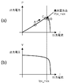
- Fig. 1 (a) shows the output current-output voltage characteristics of a typical solar cell
- Fig. 1 (b) shows the output current-output power characteristics.
- a solar cell having such characteristics is used as a DC power source.
- Such a DC power supply needs to transmit power to a load such as a storage battery at the maximum power point that is the maximum power value in order to efficiently use the output power. That is, the maximum power point tracking (Maximum Power Point Tracking) control is required, and there are several techniques for this purpose.
- Japanese Patent Application Laid-Open No. 63-57807 discloses a maximum point tracking method that detects the output voltage and output current of a solar cell and uses the differential value of the output voltage.
- This technique is a method that utilizes the fact that the differential value at the maximum power point is zero. That is, the voltage and current when a slight displacement is given to the control signal at the current operating point is detected, and after analog-to-digital (A / D) conversion, a differential value of power is obtained by calculation. Control to zero.
- This technology is expensive because it requires a microcomputer and a DSP (Digital Signal Processor) for A / D conversion and computation.
- DSP Digital Signal Processor
- Japanese Patent Laid-Open No. Sho 62-85312 discloses a maximum power point tracking method using a so-called hill-climbing method.
- this method the voltage and current values at two points are measured, the power at each point is calculated, the power values are compared, the control point is moved to the higher power value, and the control point moving direction is It is a control method that stabilizes at the point of alternately rising and falling.
- the amount of movement cannot be increased because the amount of movement of the control point continues to fluctuate across the maximum power point. If the movement amount is too small, it takes time to move the control point to the vicinity of the maximum power point, and it becomes impossible to follow the change in the output power characteristics of the solar cell.
- Japanese Patent Laid-Open No. 7-072941 discloses a method of detecting three or more voltage / current points, calculating each power, estimating a maximum power point with an approximate expression, and controlling at this estimated point. Yes.
- This method is a method of calculating each power from three or more voltage / current values according to a change in characteristics of the solar cell and finding a provisional maximum power point by an approximate expression.
- it is necessary that at least one voltage current point exceeds the maximum power point, and at least one voltage current point does not exceed the maximum power point. There is. Therefore, it is necessary to move the control point to such a voltage / current point, and the control circuit for that purpose becomes complicated and expensive.
- Japanese Patent Laid-Open No. 7-129264 discloses a method of tracking the maximum power point by detecting the operating point position from the fluctuation tendency of the output voltage of the solar cell and the output current of the power converter.
- the output change amount of the power conversion unit is digital. Will fluctuate. This is because, with respect to the characteristic change of the solar cell due to changes in the amount of solar radiation, etc., if ⁇ V is large, the output change amount of the power conversion unit will be large, so fluttering will occur. If ⁇ V is small, it will take time to stabilize. Therefore, there is a problem that the fixed ⁇ V cannot be controlled quickly and stably. Further, since the command value is changed after detecting the operating position of the solar cell from the fluctuation tendency, the delay becomes large and the responsiveness is poor.
- JP-A 63-57807 JP-A-62-85312 Japanese Patent Laid-Open No. 7-072941 JP-A-7-129264
- an inexpensive power conversion device that quickly tracks the maximum power point in the output of a DC power source such as a solar cell or a wind power generator whose output power fluctuates according to weather conditions or the like is provided. Not disclosed.
- an object of the present invention is to provide an inexpensive power conversion device that can track the maximum power point in the output of a DC power source such as a solar battery or a wind power generator whose output power varies depending on weather conditions or the like.
- Another object of the present invention is to provide a power converter that can quickly track the maximum power point in the output of a DC power source such as a solar battery or a wind power generator whose output power varies depending on weather conditions or the like. is there.
- a DC power source such as a solar battery or a wind power generator whose output power varies depending on weather conditions or the like. is there.
- a power conversion device includes (A) a D / D converter circuit that performs DC / DC conversion on an output voltage from a DC power supply having a maximum power point, and (B) an output voltage of the D / D converter circuit. And a constant voltage control for controlling the D / D converter circuit according to the difference between the voltage of the output signal of the voltage detection circuit and the reference comparison voltage.
- a constant voltage control for controlling the D / D converter circuit according to the difference between the voltage of the output signal of the voltage detection circuit and the reference comparison voltage.
- the constant voltage control circuit drives the D / D converter circuit to draw power beyond the power supply capability of the DC power supply
- the D / D is controlled regardless of the control by the constant voltage control circuit.
- the output voltage of the D converter circuit decreases, and the voltage of the output signal of the voltage detection circuit also decreases.
- the adjustment circuit operates as described above. Therefore, the constant voltage control circuit determines that the effect of its own control has appeared, and the D / D converter The drive of the circuit is returned to the level before the voltage drop of the output signal of the voltage detection circuit.
- the adjustment circuit described above includes a first detection circuit that detects a state in which a duty ratio of a signal that controls switching of a switch included in the D / D converter circuit is a predetermined maximum value, and a first detection circuit You may make it have a voltage adjustment circuit which changes the voltage of the output signal of a voltage detection circuit, or the comparison voltage used as a reference
- the first detection circuit it becomes possible to easily identify the situation in which power is drawn from the DC power supply beyond the maximum power point.
- the frequency or rate at which the detection signal is output from the first detection circuit within the predetermined period corresponds to the degree exceeding the maximum power point, the voltage of the output signal of the voltage detection circuit or the reference voltage is appropriately adjusted. Will be able to.
- the voltage adjustment circuit described above may include a circuit that switches to discharge from the discharge circuit for a period according to the frequency or rate at which the detection signal is output from the first detection circuit within a predetermined period. . Adjustment is smoothly performed according to the time constant of the discharge circuit.
- the voltage adjustment circuit described above has a first inversion circuit that inverts the polarity of the output signal of the voltage detection circuit, and the voltage of the output signal of the first inversion circuit is detected from the first detection circuit.
- An inversion signal adjustment circuit that lowers the frequency according to a frequency or a ratio that is output within a predetermined period, and a second inversion circuit that inverts the polarity of the output signal of the first inversion circuit whose voltage is reduced by the inversion signal adjustment circuit.
- the adjustment circuit described above controls the switching of the switch included in the D / D converter circuit and controls the output of the supplied power. You may make it have further.
- the constant voltage control circuit performs control so as to lengthen the ON period of the switch of the D / D converter circuit.
- the switch ON period is shortened as described above, and the target output of the D / D converter circuit is quickly reached. If the voltage is lowered, maximum power point tracking is performed at high speed.
- the constant voltage control circuit described above compares the error voltage corresponding to the difference between the voltage of the output signal of the voltage detection circuit and the reference comparison voltage with a predetermined triangular wave signal, and the error voltage is changed to a triangular wave.
- a circuit that generates a signal for turning on a switch included in the D / D converter circuit during a period exceeding the voltage of the signal may be included.
- the adjustment circuit described above may further include a limiting circuit that lowers the error voltage according to the frequency or rate at which the detection signal is output from the first detection circuit within a predetermined period.
- the switch-off period of the D / D converter circuit is formed at an appropriate timing, so that power consumption can be reduced.
- the adjustment circuit described above may be configured to gradually decrease the amount of change after the forced change of the voltage of the output signal of the voltage detection circuit or the reference comparison voltage. In this way, the extent to which power is drawn beyond the maximum power point is gradually reduced.
- a plurality of power conversion devices as described above are provided, and one power conversion device included in the plurality of power conversion devices and one DC power source included in the plurality of DC power sources are connected in a one-to-one relationship.
- a power system in which outputs of a plurality of power conversion devices are connected may be employed. With such a power system, power conversion control is performed according to the status of each DC power supply, and therefore, the entire system can be efficiently controlled with a simple configuration.
- each output of a some power converter device is controlled and connected so that it may become predetermined electric power, and is supplied to a storage battery, a load, etc.
- FIGS. 1 (a) and 1 (b) are schematic diagrams showing characteristics of solar cells.
- FIG. 2 is a functional block diagram of the system according to the first embodiment.
- FIG. 3 is a functional block diagram of a system according to the second embodiment.
- 4 (a) and 4 (b) are schematic diagrams showing the characteristics of the solar cell.
- FIGS. 5A to 5D are waveform diagrams for explaining the operation of the system according to the second embodiment.
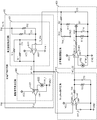
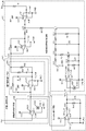
- FIG. 6 is a diagram illustrating a circuit example according to an example of the second embodiment.
- FIG. 7 is a diagram illustrating a circuit example according to an example of the second embodiment.
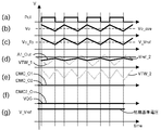
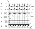
- FIGS. 8A to 8G are waveform diagrams for explaining the operation of the example of the second embodiment.
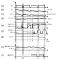
- FIG. 9A to 9I are waveform diagrams for explaining the operation of the example of the second embodiment.
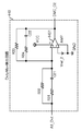
- FIG. 10 is a diagram showing a circuit of another example in the second embodiment.
- FIG. 11 is a functional block diagram of a system according to the third embodiment.
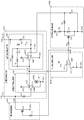
- FIG. 12 is a diagram illustrating a circuit example according to an example of the third embodiment.
- FIGS. 13A to 13G are waveform diagrams showing the operation of the circuit according to the example of the third embodiment.
- FIGS. 14A to 14I are waveform diagrams showing the operation of the circuit according to the example of the third embodiment.
- FIG. 15 is a functional block diagram of a system according to the fourth embodiment.
- 16A to 16E are waveform diagrams for explaining the operation of the system according to the fourth embodiment.
- FIG. 17 is a diagram illustrating a specific circuit example according to Example 1 of the fourth embodiment.
- FIGS. 18A to 18G are waveform diagrams for explaining the operation of example 1 of the fourth embodiment.
- FIGS. 19A to 19I are waveform diagrams for explaining the operation of example 1 of the fourth embodiment.
- FIG. 20 is a diagram illustrating another circuit example of the first example of the fourth embodiment.
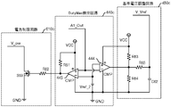
- FIG. 21 is a diagram illustrating a circuit example of the second example of the fourth embodiment.
- FIGS. 22A to 22G are waveform diagrams for explaining the operation of example 2 of the fourth embodiment.
- FIGS. 23A to 23I are waveform diagrams for explaining the operation of example 2 of the fourth embodiment.
- FIG. 24 is a functional block diagram of a system according to the fifth embodiment.
- FIG. 24 is a functional block diagram of a system according to the fifth embodiment.
- FIG. 25 is a diagram illustrating a specific circuit example according to an example of the fifth embodiment.
- FIGS. 26A to 26I are waveform diagrams for explaining the operation of example 1 of the fifth embodiment.
- FIG. 27 is a functional block diagram of a system according to the sixth embodiment.
- FIG. 28 is a functional block diagram of a system according to the sixth embodiment.
- FIG. 29 is a functional block diagram of a system according to the seventh embodiment.
- FIG. 30 is a functional block diagram of a system according to the seventh embodiment.
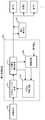
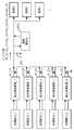
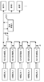
- FIG. 2 shows an example of a system including the power conversion device according to the present embodiment. That is, the system shown in FIG. 2 is a solar cell system, and is connected to the output of the solar cell 100, the power conversion device 200 that performs power conversion on the output from the solar cell 100, and the output of the power conversion device 200.
- the solar cell 100 and the load storage battery 300 are the same as the conventional one.
- the loads A to C are a device with a D / D converter circuit, a device with a D / A inverter circuit, and the like, and these are the same as conventional ones.
- the solar cell 100 is an example, and may be another natural energy generator such as a wind power generator.
- the power conversion device 200 includes (A) a D / D converter circuit 210 that DC / DC converts an output voltage from the solar cell 100, and (B) an output signal having a voltage corresponding to the output voltage of the D / D converter circuit 210. (C) a constant voltage control circuit 230 that controls the D / D converter circuit 210 according to the difference between the voltage of the output signal of the output voltage detection circuit 220 and the reference voltage; ) When the voltage of the output signal of the output voltage detection circuit 220 decreases despite the control by the constant voltage control circuit 230, the adjustment circuit 240 forcibly narrows the potential difference between the voltage of the output signal of the output voltage detection circuit 220 and the reference voltage. And have.
- the constant voltage control circuit 230 drives the D / D converter circuit 210 in an attempt to extract power beyond the power supply capability of the solar battery 100
- the constant voltage Despite the control by the control circuit 230, the output voltage of the D / D converter circuit 210 decreases, and the voltage of the output signal of the output voltage detection circuit 220 also decreases.
- the adjustment circuit 240 forcibly narrows the potential difference between the voltage of the output signal of the output voltage detection circuit 220 and the reference voltage. Then, the constant voltage control circuit 230 determines that the effect of its own control has appeared, and returns the drive of the D / D converter circuit 210 to the state before the voltage drop of the output signal of the output voltage detection circuit 220. That is, a phenomenon occurs in which the target output voltage of the D / D converter circuit 210 is lowered. As a result, the power drawn from the solar cell 100 is also reduced below its power supply capability, so that the output voltage of the D / D converter circuit 210 increases.
- Such an operation is repeated to track the maximum power point of the solar cell 100.
- a power conversion device can be configured at low cost because it can be configured without using expensive elements such as a microprocessor and a DSP.
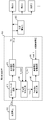
- FIG. 3 shows a functional block diagram of a system according to the second embodiment of the present invention.
- the system shown in FIG. 3 is a solar cell system, and includes a solar cell 100, a power conversion device 400 that performs power conversion on the output from the solar cell 100, and a load connected to the output of the power conversion device 400.
- the storage battery 300 and various loads A to C are connected.
- the solar cell 100 and the load storage battery 300 are the same as the conventional one.
- the loads A to C are a device with a D / D converter circuit, a device with a D / A inverter circuit, and the like, and these are the same as conventional ones.
- the solar cell 100 is an example, and may be another natural energy generator such as a wind power generator.
- the power conversion apparatus 400 includes (A) a switch, and converts the output voltage from the solar cell 100 into DC / DC by switching the switch, and (B) the output of the D / D converter circuit 410.
- An output voltage detection circuit 420 that outputs an output signal having a voltage corresponding to the voltage, and (C) the D / D converter circuit 410 is controlled according to the difference between the voltage of the output signal of the output voltage detection circuit 420 and the reference voltage.
- DutyMax detection circuit 440 and (E) the initial reference voltage is output as it is as a reference voltage, or the DutyMax detection circuit 440 It generates a reference voltage by adjusting the initial reference voltage in response to the detection signal, and a reference voltage adjusting circuit 450 to output to the constant voltage control circuit 430.
- the output power from the solar cell 100 is Ppv
- the output voltage of the power converter 400 is Vo
- the output power is Pout
- the detection voltage input from the output voltage detection circuit 420 to the constant voltage control circuit 430 is V_feed
- the constant voltage control circuit Assume that the output from 430 to the DutyMax detection circuit 440 is represented as Duty, the initial reference voltage is represented as Vref_1, and the output voltage from the reference voltage adjustment circuit 450 to the constant voltage control circuit 430 is represented as V_Vref.
- FIG. 4 (a) is basically the same as FIG. 1 (b), and shows the relationship between the output current I and the output power P of the solar cell 100.
- FIG. To explain again, when the output current I is increased up to the current Ipv_max, the output power P itself also increases. At the current Ipv_max, the output power P becomes the maximum power point Ppv_max, and when the current Ipv_max is greater than or equal to the current Ipv_max, To decrease. That is, when the current Ipv_max is exceeded, the sudden decrease in the output power P indicates that the output voltage V is also decreasing.
- a power point corresponding to a current value significantly lower than the current Ipv_max is A
- a power point corresponding to a current value in the vicinity of the current Ipv_max or more is B
- a power point corresponding to a current value in the vicinity of the current Ipv_max or less is Is C.
- power points that do not completely coincide with the power point B but have substantially the same current value are represented as B2 and B3.
- power points that do not completely coincide with the power point C but have substantially the same current value are represented as C2, C3, and the like.
- the maximum power point Ppv_max is simply expressed as M.
- FIG. 4B is exactly the same as FIG. 1A, and a description thereof will be omitted.
- FIGS. 5A to 5D show the operation of the power conversion apparatus 400 according to the present embodiment.
- the horizontal axis represents time and the vertical axis represents voltage [V].
- the power may be [W] and the duty ratio may be [%].
- FIG. 5A shows temporal changes in the output power Ppv from the solar cell 100 and the output voltage Pout of the power conversion device 400. Since there is a loss due to the power conversion device 400, the relationship Ppv> Pout is always established. For comparison, the maximum power point Ppv_max is also shown.
- FIG. 5B shows the change over time of the output voltage Vo of the power conversion device 400.
- FIG. 5C shows the change over time of the reference voltage V_Vref from the reference voltage adjustment circuit 450. An initial reference voltage Vref_1 is also shown for comparison.
- FIG. 5D shows the time change of the output duty of the constant voltage control circuit 430. Note that a maximum value DutyMax predetermined for the output duty is also shown for comparison.
- the D / D converter circuit 410, the output voltage detection circuit 420, and the constant voltage control are performed until the output power from the solar battery 100 reaches the power point M from the power smaller than the power point A to the power point A.
- the voltage control circuit 430 switches the switch of the D / D converter circuit 410.
- the constant voltage control circuit 430 operates so as to gradually increase the duty ratio of the switching pulse with respect to the switch of the D / D converter circuit 410 and the duty voltage. If it does in this way, as shown in Drawing 5 (b), output voltage Vo of power converter 400 will be maintained constant.
- the constant voltage control circuit 430 detects that the difference between Vo (ie, V_feed) and V_Vref has increased, and sets the duty ratio of the switching pulse to the switch of the D / D converter circuit 410 and the voltage of the signal Duty to DutyMax. Raise to.
- the DutyMax detection circuit 440 detects that the voltage of the signal Duty has reached DutyMax, and outputs a detection signal to the reference voltage adjustment circuit 450.
- the reference voltage adjustment circuit 450 adjusts the initial reference voltage Vref_1 to be lowered according to the detection signal from the DutyMax detection circuit 440, and outputs the adjusted voltage V_Vref to the constant voltage control circuit 430. This state is shown in FIG.
- the amount by which the reference voltage V_Vref is reduced is determined according to the frequency or rate at which the detection signal is output from the DutyMax detection circuit 440 within a predetermined period.
- the constant voltage control circuit 430 drives the D / D converter circuit 410 too much, the power drawn from the solar cell 100 also decreases, and the power and the actual power of the solar cell 100 are reduced.
- the output power Ppv is balanced at the power point B. As a result, the output voltage Vo and the output power Pout of the power conversion device 400 stop decreasing.
- the constant voltage control circuit 430 detects that the difference between Vo (ie, V_feed) and V_Vref is small, and generates a switching pulse for the switch of the D / D converter circuit 410.
- the duty ratio and the signal Duty voltage are reduced.
- the current drawn from the solar cell 100 is reduced by driving the D / D converter circuit 410 by the constant voltage control circuit 430.
- the amount of decrease in the current drawn from the solar cell 100 is somewhat larger, so that the current passes through the maximum power point M and returns to the power point C as shown in FIG.
- the adjustment of the reference voltage V_Vref by the reference voltage adjustment circuit 450 is delayed, and even if the DutyMax detection circuit 440 decreases the voltage of the signal DutyMax from the DutyMax, the adjustment is finished immediately.
- the reference voltage V_Vref gradually increases.
- the constant voltage control circuit 430 drives the D / D converter circuit 410 in accordance with the difference between the output voltage Vo (ie, V_feed) and the reference voltage V_Vref, and thereby the solar cell 100. Therefore, the duty ratio of the switching pulse with respect to the switch of the D / D converter circuit 410 and the voltage of the signal Duty are increased so as to draw more power from.
- the output power Ppv of the solar cell 100 rises and reaches the power point M again.
- the subsequent operation is almost the same as that after the power point M is first reached.
- the reference voltage V_Vref has not returned to the initial reference voltage Vref_1, and the output voltage Vo of the power converter 400 has not reached the target value.
- the reduction width of the voltage V_Vref is slightly different. Since the operations are not completely the same as described above, the operation on the curve in FIG. 4B is switched at C1 and C2 instead of the power point C and at B1 and B2 instead of the power point B.
- the power point B or its vicinity and the power point C or its vicinity are moved back and forth across the maximum power point. That is, maximum power point tracking is possible.
- the operation described above is based on the assumption that the generated power of the solar cell 100 is constant. However, since the generated power is generally not constant, the maximum power point itself varies, but the operation is the same.
- the difference between the power point B and the power point C is determined according to the output power and the output voltage, but can be adjusted by adjusting the gain of the control system including the D / D converter circuit 410 and the like. That is, it can be operated near the maximum power point.
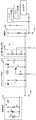
- FIG. 6 shows a specific circuit example of the solar battery 100, a specific circuit example of the D / D converter circuit 410, a specific circuit example of the output voltage detection circuit 420, and a specific circuit example of the storage battery 300. Yes.
- the solar cell 100 is shown as an equivalent circuit including a current source Icc, a diode D1, and resistors R1 and R2.
- the anode of the diode D1 and one end of the resistor R1 and one end of R2 are connected to the positive terminal of the current source Icc, and the negative terminal of the current source Icc is grounded together with the cathode of the diode D1 and the other end of the resistor R2. It is connected to the.
- the other end of the resistor R1 is connected to the D / D converter circuit 410.
- the D / D converter circuit 410 in FIG. 6 is shown as a step-up chopper circuit, a half-bridge circuit method, a full-bridge circuit method, a push-pull circuit method, a forward circuit method, a flyback method, a step-down chopper circuit, a SEPIC, With a buck-boost circuit such as a Cuk converter or a Zeta converter, an insulating type or a non-insulating type can be selected according to the application.
- the D / D converter circuit 410 includes diodes D2 and D3 for preventing backflow, an electrolytic capacitor C1, a capacitor C2, a coil L1, an FET (S1) switched by the constant voltage control circuit 430, and a resistor R3.
- the anode of the diode D2 is connected to the resistor R1 of the solar cell 100, and the cathode of the diode D2 is connected to the plus (+) terminal of the electrolytic capacitor C1 and one end of the coil L1.
- the negative ( ⁇ ) terminal of the electrolytic capacitor C1 is grounded.
- the other end of the coil L1 is connected to the drain terminal of the FET (S1) and the anode of the diode D3.
- the source terminal of the FET (S1) is grounded, and the gate terminal of the FET (S1) is connected to one end of the resistor R3.
- the other end of the resistor R3 is connected to the output of the drive signal generation circuit 432 of the constant voltage control circuit 430 through the connection terminal A.
- the cathode of the diode D3 is connected to one end of the capacitor C2 and the output voltage detection circuit 420.
- the other end of the capacitor C2 is grounded.
- the backflow prevention diodes D2 and D3 can be omitted.
- the output voltage detection circuit 420 includes resistors R4 and R5 for detecting a feedback voltage by resistance division.
- One end of the resistor R4 is connected to the D / D converter circuit 410 and the storage battery 300.
- the other end of the resistor R4 is connected to one end of the resistor R5 and the voltage error detection circuit 431 of the constant voltage control circuit 430 through the connection terminal B.
- the other end of the resistor R5 is grounded.
- the storage battery 300, the DC / AC inverter circuit corresponding to the loads A to C, the DC / DC converter circuit, and other loads are the same as those in the prior art, and further description is omitted.
- FIG. 7 shows specific circuit examples of the constant voltage control circuit 430, the DutyMax detection circuit 440, and the reference voltage adjustment circuit 450 according to the present embodiment.
- the constant voltage control circuit 430 is, for example, a PID control circuit, and includes a voltage error detection circuit 431 and a drive signal generation circuit 432.
- the voltage error detection circuit 431 is connected to the output voltage detection circuit 420 through the connection terminal B, and includes resistors R11 to R14, capacitors C11 and C12, and an operational amplifier 4311.
- the output of the output voltage detection circuit 420 is connected to one ends of the resistors R11 and R12, the other end of the resistor R11 is connected to one end of the capacitor C11, and the other end of the capacitor C11 and the other end of the resistor R12 are the negative electrode of the operational amplifier 4311. Is connected to the side input terminal.
- the negative input terminal of the operational amplifier 4311 is connected to one end of the capacitor C12 and one end of the resistor R13, the other end of the capacitor C12 is connected to one end of the resistor R14, and the other end of the resistor R14 and the resistor R13. The other end is connected to the output terminal of the operational amplifier 4311. Further, the output of the reference voltage adjustment circuit 450 is connected to the positive input terminal of the operational amplifier 4311.
- the drive signal generation circuit 432 includes a comparator 4321 and a triangular wave generator 4322.
- the output terminal of the voltage error detection circuit 431 is connected to the positive input terminal of the comparator 4321, and the triangular wave generator 4322 is connected to the negative input terminal of the comparator 4321.
- the output terminal of the comparator 4321 is connected to the gate terminal of the FET (S1) of the D / D converter circuit 410 via the connection terminal A.
- the DutyMax detection circuit 440 includes a comparator 441, resistors R15 and R16, a capacitor C13, and a DC power supply Vref_2 that outputs a voltage Vref_2.
- the positive input terminal of the comparator 441 is connected to the output terminal of the operational amplifier 4311 of the voltage error detection circuit 431, and the negative input terminal of the comparator 441 is connected to the positive terminal of the DC power supply Vref_2.
- the negative terminal of the DC power supply Vref_2 is grounded.
- the output of the comparator 441 is connected to one end of the resistor R15, and the other end of the resistor R15 is connected to one end of the resistor R16, one end of the capacitor C13, and the input of the reference voltage adjustment circuit 450.
- the other end of the resistor R16 and the other end of the capacitor C13 are grounded.
- the comparator 441 of the DutyMax detection circuit 440 is input to the drive signal generation circuit 432 when the duty ratio between the input signal A1_Out to the drive signal generation circuit 432 and the switching pulse output from the drive signal generation circuit 432 is maximized.
- the DC power supply Vref_2 that outputs substantially the same voltage as the signal A1_Out is compared.
- the comparator 441 outputs a pulse wave DMC_O1 during that time.
- a low-pass filter is connected to the output of the comparator 441, and the output pulse wave is output to the reference voltage adjustment circuit 450 as a smooth signal DMC_O2.
- the reference voltage adjustment circuit 450 includes a comparator 451, a triangular wave generator 452, resistors R17 to R21, an FET (S11), a DC power supply Vref_1 that outputs an initial reference voltage Vref_1, and capacitors C14 and C15.
- the output of the DutyMax detection circuit 440 is connected to the positive input terminal of the comparator 451, and the triangular wave generator 452 is connected to the negative input terminal of the comparator 451.
- One end of the resistor R17 is connected to the output of the comparator 451, and the other end of the resistor R17 is connected to one end of the resistor R18, one end of the capacitor C14, and the gate terminal of the FET (S11).
- the other end of the resistor R18, the other end of the capacitor C14, and the source terminal of the FET (S11) are grounded.
- the positive terminal of the DC power supply Vref_1 is connected to one end of the resistor R19, and the negative terminal is grounded.
- the other end of the resistor R19 is connected to one end of the resistor R20 and one end of the resistor R21, and the other end of the resistor R20 is connected to the drain terminal of the FET (S11).
- the other end of the resistor R21 is connected to one end of the capacitor C15 and the positive terminal of the operational amplifier 4311 of the voltage error detection circuit 431.
- the other end of the capacitor C15 is grounded.
- the DC power supply Vref_1 of the reference voltage adjusting circuit 450 charges the capacitor C15 while the FET (S11) is off.
- the FET (S11) is turned on, the capacitor C15 discharges the stored charge, so that the voltage that changes depending on the amount of charge held in the capacitor C15 becomes the output V_Vref.
- the comparator 451 of the reference voltage adjustment circuit 450 compares the output DMC_O2 of the DutyMax detection circuit 440 with the triangular wave, and outputs the pulse wave DMC2_O when the voltage of the output signal DMC_O2 becomes larger than the triangular wave.
- the signal VQG obtained by smoothing the pulse wave DMC2_O is input to the gate terminal of the FET (S11).
- the ON / OFF state of the FET (S11) is determined by the signal VQG, and the discharging period of the capacitor C15 is also determined. Further, the output reference voltage V_Vref is also determined.
- FIGS. 8A to 8G show operations for a short time, and are diagrams for explaining basic operations of the circuits shown in FIGS. 6 and 7.
- FIG. 8A shows the switching pulse Pul that is the output of the drive signal generation circuit 432.
- the duty ratio is substantially constant.
- the average value Vo_ave of the voltage of the output signal Vo of the D / D converter circuit 410 is also constant only by the fluctuation to such an extent that ripples are generated according to switching.
- the DutyMax detection circuit 440 and the reference voltage adjustment circuit 450 are not operating, and the initial reference voltage Vref_1 becomes the output voltage V_Vref of the reference voltage adjustment circuit 450. Yes.
- the voltage error detection circuit 431 compares Vo_fb and V_Vref, and as shown in FIG. 8D, the voltage output signal A1_Out is obtained by inverting the difference between Vo_fb and V_Vref. Is output.
- the voltage of the output signal A1_Out is lower than the voltage Vref_2 used as a reference in the DutyMax detection circuit 440 and corresponding to the maximum duty ratio.
- the DutyMax detection circuit 440 and the reference voltage adjustment circuit 450 do not operate. The state of not operating is shown in FIGS.
- the output side signals DMC_O1 and DMC_O2 of the comparator 441 of the DutyMax detection circuit 440 remain zero. Further, even when the comparator 451 of the reference voltage adjustment circuit 450 compares the triangular wave VTW_2 and DMC_O2, the signals DMC2_O and VQG on the output side of the comparator 451 remain zero because DMC_O2 remains zero. Then, since the FET (S11) of the reference voltage adjusting circuit 450 remains off, as shown in FIG. 8G, the output voltage V_Vref of the capacitor C15 changes with the initial reference voltage Vref_1 of the DC power supply Vref_1 being changed. do not do.
- FIGS. 9A to 9I are drawn so as to emphasize the features of the present embodiment, there are some differences from actual ones.
- the D / D converter circuit 410 attempts to draw power.
- the duty ratio of the switching pulse with respect to the gate terminal of the FET (S1) of the / D converter circuit 410 is maximized.
- the output Vo of the D / D converter circuit 410 is lowered.
- FIG. 9C when the output Vo decreases, the output Vo_fb of the output voltage detection circuit 420 also decreases.
- the voltage error detection circuit 431 inverts the difference from the current V_Vref, if the Vo_fb of the output voltage detection circuit 420 decreases, the output A1_Out of the voltage error detection circuit 431 increases on the contrary. Then, as shown in FIG. 9 (d), the voltage of the output A1_Out of the voltage error detection circuit 431 gradually corresponds to the maximum value of the duty ratio of the switching pulse in the switching period for the FET (S1). The period exceeding Vref_2 becomes longer. As shown in FIG. 9E, the period during which the output DMC_O1 of the comparator 441 of the DutyMax detection circuit 440 is turned on gradually increases. Further, as shown in FIG.
- the output DMC_O2 of the DutyMax detection circuit 440 is a signal after the DMC_O1 is smoothed by the low-pass filter.
- the voltage gradually increases. To rise.
- the output DMC2_O of the comparator 451 of the reference voltage adjustment circuit 450 is turned on as shown in FIG.
- a signal VQG as shown in FIG. 9F is generated.
- This signal VQG turns on / off the FET (S11) of the reference voltage adjusting circuit 450.
- the FET (S11) When the FET (S11) is turned on, the capacitor C15 is discharged. Therefore, the reference voltage V_Vref decreases as the discharge time increases and the discharge frequency increases.
- FIG. 9 (f) when the frequency (or rate) at which the duty ratio of the switching pulse is maximized within a predetermined period in the past, a period in which the signal VQG is not 0 frequently occurs. become longer.
- the reference voltage V_Vref gradually decreases.
- the electric power drawn from the solar cell 100 is lowered as described above, so that the output Vo of the D / D converter circuit 410 increases. Thereafter, if the D / D converter circuit 410 operates so as to draw power from the solar cell 100, the voltage Vo decreases as shown in FIG. 9B. Therefore, the operation described above is repeated. become. That is, the maximum power point is tracked.
- the constant voltage control circuit 430 a conventional constant voltage control circuit can be used. Also, the DutyMax detection circuit 440 can be replaced with a DutyMax detection circuit 445 as shown in FIG.
- the DutyMax detection circuit 445 includes resistors R31 to R34, capacitors C21 and C22, an operational amplifier 4451, and a DC power supply Vref_2.
- the DC power supply Vref_2 outputs a voltage substantially the same as the voltage of the input signal A1_Out input to the drive signal generation circuit 432 when the duty ratio of the switching pulse that is the output of the drive signal generation circuit 432 becomes maximum.
- the output A1_Out of the voltage error detection circuit 431 is connected to one end of the resistor R32 and one end of the resistor R31, the other end of the resistor R31 is connected to one end of the capacitor C21, and the other end of the capacitor C21 is connected to the resistor R32.
- the other end and the positive input terminal of the operational amplifier 4451 are connected.
- the positive input terminal of the operational amplifier 4451 is further connected to one end of the resistor R33 and one end of the resistor R34.
- the other end of the resistor R34 is connected to one end of the capacitor C22, and the other end of the capacitor C22 is connected to the other end of the resistor R33 and the output of the operational amplifier 4451.
- the negative input terminal of the operational amplifier 4451 is connected to the positive terminal of the DC power supply Vref_2, and the negative terminal of the DC power supply Vref_2 is grounded.
- Such a DutyMax detection circuit 445 outputs a signal DMC_O2 having a voltage corresponding to the difference between the voltage of the output A1_Out of the voltage error detection circuit 431 and the voltage Vref_2. That is, as shown in FIG. 9 (d), when the output A1_Out exceeds the voltage Vref_2, DMC_O2 rises by that amount, so that the change is similar to that of DMC2_O shown in FIG. 9 (f).
- FIG. 11 shows a functional block diagram of a system according to the third embodiment.
- the system shown in FIG. 11 is a solar cell system, and includes a solar cell 100, a power conversion device 500 that performs power conversion on the output from the solar cell 100, and a load connected to the output of the power conversion device 500. It has a storage battery 300 and various loads A to C. Solar cell 100, load storage battery 300, and loads A to C are the same as in the second embodiment.
- the power conversion apparatus 500 includes (A) a switch, and a D / D converter circuit 510 that DC / DC converts an output voltage from the solar cell 100 by switching the switch, and (B) an output of the D / D converter circuit 510.
- An output voltage detection circuit 520 that outputs an output signal of a voltage corresponding to the voltage to the voltage detection signal adjustment circuit 530, and (C) adjusts the detection signal from the output voltage detection circuit 520 according to the output from the DutyMax detection circuit 550,
- a voltage detection signal adjustment circuit 530 that outputs a detection signal after adjustment, and a D / D converter circuit 510 according to the difference between (D) the fixed reference voltage and the voltage of the detection signal after adjustment from the voltage detection signal adjustment circuit 530
- a constant voltage control circuit 540 that controls the output of the D / D converter circuit 510 and (E) The duty ratio of the switching pulse for instructing off and a DutyMax detection circuit 550 for detecting a state in which a predetermined maximum value.
- the operation of the power conversion device 500 shown in FIG. 11 is basically the same as that of the power conversion device 400 of the second embodiment.
- the reference voltage V_Vref is not adjusted, but the reference voltage V_Vref is fixed, and the voltage of the detection signal of the output voltage detection circuit 520 is the object of adjustment.
- the degree of adjustment is the same as in the second embodiment, and is determined according to the frequency (or ratio) at which the state in which the duty ratio of the switching pulse is a predetermined maximum value is detected within a predetermined period.
- the constant voltage control circuit 540 sets the duty ratio of the switching pulse to a predetermined maximum value. Then, try to raise the voltage further.
- the DutyMax detection circuit 550 transmits a detection signal to the voltage detection signal adjustment circuit 530 when detecting that the duty ratio of the switching pulse is a predetermined maximum value.
- the voltage detection signal adjustment circuit 530 increases the voltage of the detection signal of the output voltage detection circuit 520 according to the frequency (or rate) of detecting the state where the duty ratio of the switching pulse is a predetermined maximum value within a predetermined period.
- the difference from the reference voltage V_Vref is narrowed.
- the power drawn from the solar cell 100 by driving the D / D converter circuit 510 by the constant voltage control circuit 540 also decreases, and the power and the output power of the solar cell 100 are the power point B in FIG. Will be balanced. As a result, the output voltage Vo and the output power Pout of the power conversion device 500 stop decreasing.
- the constant voltage control circuit 540 reduces the duty ratio of the switching pulse from a predetermined maximum value. Further, the adjustment amount of the detection signal after adjustment has a time constant, and does not immediately become 0, so it gradually decreases.
- the parts other than such an operation are almost the same as those in the second embodiment. Therefore, as in the second embodiment, the maximum power point can be traced by an inexpensive circuit element.
- FIG. 12 shows a specific circuit example in the third embodiment.
- the solar cell 100 is the same as in the second embodiment, and the D / D converter circuit 510 is the same as the D / D converter circuit 410 in the second embodiment. Since the output voltage detection circuit 520 is the same as the output voltage detection circuit 420 in the second embodiment, the illustration is omitted.
- the constant voltage control circuit 540 is, for example, a PID control circuit, and includes a voltage error detection circuit 541 and a drive signal generation circuit 542.
- the voltage error detection circuit 541 is connected to the output of the voltage detection signal adjustment circuit 530, and includes resistors R41 to R44, capacitors C41 and C42, and an operational amplifier 5411.
- the output of the voltage detection signal adjustment circuit 530 is connected to one ends of the resistors R41 and R42, the other end of the resistor R41 is connected to one end of the capacitor C41, and the other end of the capacitor C41 and the other end of the resistor R42 are connected to the operational amplifier 5411. Connected to the negative input terminal.
- the negative input terminal of the operational amplifier 5411 is connected to one end of the capacitor C42 and one end of the resistor R43, the other end of the capacitor C42 is connected to one end of the resistor R44, and the other end of the resistor R44 and the other end of the resistor R43. The end is connected to the output terminal of the operational amplifier 5411. Further, the positive terminal of the operational amplifier 5411 is connected to the positive terminal of the DC power source V_Vref that outputs a fixed reference voltage V_Vref. Note that the negative terminal of the DC power supply V_Vref is grounded.
- the drive signal generation circuit 542 includes a comparator 5421 and a triangular wave generator 5422.
- the output terminal of the voltage error detection circuit 541 is connected to the positive input terminal of the comparator 5421, and the triangular wave generator 5422 is connected to the negative input terminal of the comparator 5421.
- the output terminal of the comparator 5421 is connected to the gate terminal of the FET (S1) of the D / D converter circuit 510 via the connection terminal A.
- the DutyMax detection circuit 550 includes a comparator 551, resistors R45 and R46, a capacitor C43, and a DC power supply Vref_2 that outputs a voltage Vref_2.
- the positive input terminal of the comparator 551 is connected to the output terminal of the operational amplifier 5411 of the voltage error detection circuit 541, and the negative input terminal of the comparator 551 is connected to the positive terminal of the DC power supply Vref_2.
- the negative terminal of the DC power supply Vref_2 is grounded.
- the output of the comparator 551 is connected to one end of the resistor R45, and the other end of the resistor R45 is connected to one end of the resistor R46, one end of the capacitor C43, and the input of the voltage detection signal adjustment circuit 530.
- the other end of the resistor R46 and the other end of the capacitor C43 are grounded.
- the comparator 551 of the DutyMax detection circuit 550 is input to the drive signal generation circuit 542 when the duty ratio of the input signal A1_Out to the drive signal generation circuit 542 and the switching pulse output from the drive signal generation circuit 542 is maximized.
- the DC power supply Vref_2 that outputs substantially the same voltage as the signal A1_Out is compared.
- the comparator 551 outputs a pulse wave DMC_O1 during that time.
- a low-pass filter is connected to the output of the comparator 551, and the output pulse wave is output to the voltage detection signal adjustment circuit 530 as a smooth signal wave DMC_O2.
- the voltage detection signal adjustment circuit 530 outputs a comparator 534, a triangular wave generator 535, operational amplifiers 531 and 532, resistors R51 to R62, FET (S51), transistor T1, capacitors C51 and C52, and a voltage V_Vref.
- a DC power supply V_Vref that outputs a predetermined voltage Vref_3.
- the triangular wave generator 535 is connected to the positive input terminal of the comparator 534, and the output of the DutyMax detection circuit 550 is connected to the negative input terminal of the comparator 534.
- One end of the resistor R56 is connected to the output terminal of the comparator 534, and one end of the resistor R57, one end of the capacitor C51, and the gate terminal of the FET (S51) are connected to the other end of the resistor R56.
- the other end of the resistor R57 and the other end of the capacitor C51 are grounded.
- the source terminal of the FET (S51) is grounded, and the drain terminal is connected to one end of the resistor R61.
- the other end of the resistor R61 is connected to one end of the resistor R58 and one end of the resistor R59.
- the other end of the resistor R58 is connected to the positive terminal of the DC power supply Vref_3, and the negative terminal of the DC power supply Vref_3 is grounded. Further, the other end of the resistor R59 is connected to one end of the resistor R60 and one end of the capacitor C52. The other end of the capacitor C52 is grounded. The other end of the resistor R60 is connected to one end of the resistor R62 and the base terminal of the transistor T1. Further, the other end of the resistor R62 is grounded. The emitter of the transistor T1 is grounded, and the collector is connected to one end of the resistor R55.
- one end of the resistor R51 is connected to the output of the output voltage detection circuit 520, and the other end of the resistor R51 is connected to one end of the resistor R52 and the negative input terminal of the operational amplifier 531.
- the positive input terminal of the operational amplifier 531 is connected to the positive terminal of the DC power supply V_Vref, and the negative terminal of the DC power supply V_Vref is grounded.
- the other end of the resistor R52 is connected to the output terminal of the operational amplifier 531, the other end of the resistor R55, and one end of the resistor R53.
- the other end of the resistor R53 is connected to one end of the resistor R54 and the negative input terminal of the operational amplifier 532.
- the positive input terminal of the operational amplifier 532 is connected to the positive terminal of the DC power supply V_Vref, and the negative terminal of the DC power supply V_Vref is grounded.
- the other end of the resistor R54 is connected to the output terminal of the operational amplifier 532 and the input of the voltage error detection circuit 541 of the constant voltage control circuit 540.
- the comparator 534 compares the output VTW_3 of the triangular wave generator 535 and the output of the DutyMax detection circuit 550. As long as the duty ratio of the switching pulse does not become the maximum value, the voltage of the output VTW_3 is the output DMC_O2 of the DutyMax detection circuit 550. Since the voltage is higher than the output voltage, the high output DMC2_O is always output. On the other hand, when the duty ratio of the switching pulse reaches the maximum value, the voltage of the output DMC_O2 of the DutyMax detection circuit 550 increases, so that the period in which the output DMC2_O is turned off gradually increases.
- the FET (S51) Since a low pass filter is provided on the output side of the comparator 534, the FET (S51) is turned on / off by the signal VQG smoothed by the low pass filter. However, the FET (S51) is normally on, and no charge is stored in the capacitor C52. As the OFF period becomes longer, the voltage is gradually stored in the capacitor C52 and becomes higher. On the other hand, when the voltage of the capacitor C52 increases, the voltage VQB applied to the base terminal of the transistor T1 also increases and the transistor T1 also turns on. In this case, the output voltage of the operational amplifier 531 is lowered. .
- the output Vo_fb of the output voltage detection circuit 520 is inverted, so that when the transistor T1 is turned on, the voltage of the output Vof2 of the operational amplifier 531 is further lowered.
- the operational amplifier 532 inverts the output Vof2 again and outputs the output Vof3 to the voltage error detection circuit 541 as the output of the voltage detection signal adjustment circuit 530. More specifically, when Vof2 is lowered, Vof3 is raised, and the voltage error detection circuit 541 of the constant voltage control circuit 540 has a voltage error detection circuit 540 as if the output Vo_fb of the output voltage detection circuit 520 is increased. Is visible.
- FIGS. 13A to 13G show an operation for a short time, and are diagrams for explaining the basic operation of the circuit shown in FIG.
- FIG. 13A shows a switching pulse that is an output of the drive signal generation circuit 542.
- the duty ratio is substantially constant.
- the average value Vo_ave of the voltage of the output signal Vo of the D / D converter circuit 510 is also constant only by the fluctuation to such an extent that ripples are generated according to switching.
- the DutyMax detection circuit 550 and the voltage detection signal adjustment circuit 530 are not operating, and the output Vo_fb of the output voltage detection circuit 520 and the voltage detection signal adjustment circuit 530 are not operated.
- the output Vof3 is almost the same.
- the voltage of the output signal A1_Out is lower than the voltage Vref_2 used as a reference in the DutyMax detection circuit 550 and corresponding to the maximum duty ratio.
- the DutyMax detection circuit 550 and the voltage detection signal adjustment circuit 530 do not operate. The state of not operating is shown in FIGS. 13 (e) to 13 (g).
- both the output side signals DMC_O1 and DMC_O2 of the comparator 551 of the DutyMax detection circuit 550 remain zero. Further, even if the comparator 534 of the voltage detection signal adjustment circuit 530 compares the triangular wave VTW_3 and DMC_O2, the signal DMC2_O and VQG on the output side of the comparator 534 remain high because DMC_O2 remains 0. Then, since the FET (S51) of the voltage detection signal adjustment circuit 530 remains on, as shown in FIG. 13F, the voltage of the capacitor C52 applied to the base terminal of the transistor T1 turns on the transistor T1. The voltage does not become low and remains low.
- the D / D converter circuit 510 attempts to draw current.
- the duty ratio of the switching pulse with respect to the gate terminal of the FET (S1) of the / D converter circuit 510 is maximized.
- the output Vo of the D / D converter circuit 510 is lowered.
- FIG. 14C when the output Vo decreases, the output Vo_fb of the output voltage detection circuit 520 also decreases.
- the voltage error detection circuit 541 inverts the difference from the fixed V_Vref. Therefore, when the output Vo_fb of the output voltage detection circuit 520 decreases and the adjustment of Vof2 is not performed, the output of the voltage error detection circuit 541 A1_Out will rise on the contrary. Then, as shown in FIG. 14D, the voltage of the output A1_Out of the voltage error detection circuit 541 gradually corresponds to the maximum value of the duty ratio of the switching pulse in the switching period for the FET (S51). The period exceeding Vref_2 becomes longer. As shown in FIG. 14E, the period during which the output DMC_O1 of the comparator 551 of the DutyMax detection circuit 550 is turned on gradually increases. Further, as shown in FIG.
- the output DMC_O2 of the DutyMax detection circuit 550 is a signal after the DMC_O1 is smoothed by the low-pass filter. However, since the DMC_O1 is turned on longer, the voltage gradually increases. To rise. Up to this point, the operation is almost the same as that described for the specific circuit example of the second embodiment.
- the output DMC2_O of the comparator 534 of the voltage detection signal adjustment circuit 530 is turned on as shown in FIG.
- the signal DMC2_O is also smoothed by a low-pass filter to generate a signal VQG (not shown).
- This signal VQG turns on / off the FET (S51) of the voltage detection signal adjustment circuit 530.
- the FET (S51) is off and the capacitor A state where the battery is discharged from C52 is normal.
- the duty ratio of the switching pulse when the duty ratio of the switching pulse is maximized, the period during which the FET (S51) is turned off becomes longer and frequently turned off, and as shown in FIG.
- the applied voltage VQB increases. That is, when the frequency (or rate) at which the duty ratio of the switching pulse is maximized becomes high within a predetermined period in the past, the frequency and period during which the transistor T1 is turned on becomes longer, as shown by the solid line in FIG.
- the output voltage Vof2 of the operational amplifier 531 of the voltage detection signal adjustment circuit 530 is lowered.
- the dotted line represents the curve when no adjustment is made. Then, the output Vof3 of the voltage detection signal adjustment circuit 530 increases on the contrary.
- the ON width of the switching pulse (represented as corrected Pul) is shortened. That is, from the constant voltage control circuit 540, the duty ratio is increased, the ON period of the FET (S1) of the D / D converter circuit 510 is lengthened, and operation is performed to draw more power from the solar cell 100. As a result, it seems as if this operation was effective. Therefore, the difference between the voltage of the output Vof3 of the voltage detection signal adjustment circuit 530 and the reference voltage V_Vref is reduced, so that the duty ratio is lowered.
- the electric power drawn from the solar cell 100 is lowered as described above, so that the output Vo of the D / D converter circuit 510 is increased.
- the voltage Vo will decrease as shown in FIG. 14B, so that the operation as described above is repeated. become. That is, the maximum power point is tracked.
- the fourth embodiment is a modification of the second embodiment.
- FIG. 15 shows a functional block diagram of a system according to the fourth embodiment of the present invention.
- the system shown in FIG. 15 is a solar cell system, and includes a solar cell 100, a power conversion device 600 that performs power conversion on the output from the solar cell 100, and a load connected to the output of the power conversion device 600. It has a storage battery 300 and various loads A to C.
- the solar cell 100, the load storage battery 300, and the loads A to C are the same as those in the second embodiment.
- the power conversion apparatus 600 includes (A) a switch, and a D / D converter circuit 410 that DC / DC converts an output voltage from the solar cell 100 by switching the switch, and (B) an output of the D / D converter circuit 410.
- An output voltage detection circuit 420 that outputs an output signal having a voltage corresponding to the voltage, and (C) the D / D converter circuit 410 is controlled according to the difference between the voltage of the output signal of the output voltage detection circuit 420 and the reference voltage.
- a constant voltage control circuit 620 and (D) detecting a state in which the duty ratio of a switching pulse output from the constant voltage control circuit 620 and instructing on / off of the switch of the D / D converter circuit 410 is a predetermined maximum value DutyMax detection circuit 440 and (E) the initial reference voltage is output as it is as the reference voltage, or the DutyMax detection circuit 44
- a reference voltage adjustment circuit 450 that adjusts an initial reference voltage according to the detection signal of the reference signal to generate a reference voltage and outputs the reference voltage to the constant voltage control circuit 620, and (F) a constant voltage according to the detection signal of the DutyMax detection circuit 440 And a power limiting circuit 610 for processing the switching pulse of the control circuit 620.
- the duty ratio of the switching pulse is forcibly lowered.
- the output power from the solar cell 100 is Ppv
- the output voltage of the power converter 600 is Vo
- the output power is Pout
- the constant voltage control circuit 620 to the DutyMax detection circuit 440 Assume that the output is Duty
- the initial reference voltage is Vref_1
- the output voltage from the reference voltage adjustment circuit 450 to the constant voltage control circuit 620 is V_Vref.
- FIG. 16A shows the change over time of the output power Ppv from the solar cell 100 and the output voltage Pout of the power converter 600. Since there is a loss due to power conversion device 600, the relationship Ppv> Pout is always established. For comparison, the maximum power point Ppv_max is also shown.
- FIG. 16B shows the change over time of the output voltage Vo of the power converter 600.
- FIG. 16C shows the time change of the reference voltage V_Vref from the reference voltage adjustment circuit 450. An initial reference voltage Vref_1 is also shown for comparison.
- FIG. 16D shows the time change of the output duty of the constant voltage control circuit 620. Note that a maximum value DutyMax predetermined for the output duty is also shown for comparison.
- the D / D converter circuit 410, the output voltage detection circuit 420, and the constant voltage control are performed until the output power from the solar battery 100 reaches the power point M from the power smaller than the power point A to the power point A.
- the voltage control circuit 620 switches the switch of the D / D converter circuit 410.
- the output V_feed of the output voltage detection circuit 420 is lowered simply by driving the D / D converter circuit 410 as before. . Due to this decrease, the constant voltage control circuit 620 operates so as to gradually increase the duty ratio of the switching pulse to the switch of the D / D converter circuit 410 and the duty voltage, as shown in FIG. In this way, as shown in FIG. 16B, the output voltage Vo of the power converter 600 is maintained substantially constant.
- the constant voltage control circuit 620 detects that the difference between Vo (ie, V_feed) and V_Vref has increased, and sets the duty ratio of the switching pulse to the switch of the D / D converter circuit 410 and the voltage of the signal Duty to DutyMax. Raise to.
- the DutyMax detection circuit 440 detects that the voltage of the signal Duty has reached DutyMax, and outputs a detection signal to the reference voltage adjustment circuit 450 and the power limiting circuit 610.
- the reference voltage adjustment circuit 450 adjusts the initial reference voltage Vref_1 to be lowered according to the detection signal from the DutyMax detection circuit 440, and outputs the adjusted voltage V_Vref to the constant voltage control circuit 620. This is shown in FIG.
- the amount by which the reference voltage V_Vref is reduced is determined according to the frequency or rate at which the detection signal is output from the DutyMax detection circuit 440 within a predetermined period.
- the power limiting circuit 610 lowers the power extraction level from the solar cell 100 by the D / D converter circuit 410 at an early stage. Therefore, according to the detection signal from the DutyMax detection circuit 440, the switching of the switch of the D / D converter circuit 410 is controlled separately from the signal Duty output from the constant voltage control circuit 620 to the DutyMax detection circuit 440. It acts on the constant voltage control circuit 620 to pull down the signal, for example, the switching pulse itself or the signal used to generate the switching pulse. As a result, as indicated by a dotted line in FIG. 16E, the duty ratio of the switching pulse is temporarily reduced.
- the constant voltage control circuit 620 detects that the difference between Vo (ie, V_feed) and V_Vref is small, and generates a switching pulse for the switch of the D / D converter circuit 410.
- the duty ratio and the signal Duty voltage are reduced.
- the current drawn from the solar cell 100 is reduced by driving the D / D converter circuit 410 by the constant voltage control circuit 620.
- the amount of decrease in the current drawn from the solar cell 100 is somewhat larger, so that the current passes through the maximum power point M and returns to the power point C as shown in FIG.
- the output power Ppv of the solar cell 100 once increases but decreases again.
- the output voltage Vo of the power conversion device 600 gradually increases at the drive level of the D / D converter circuit 410 during this period.
- the adjustment of the reference voltage V_Vref by the reference voltage adjustment circuit 450 is delayed, and even if the DutyMax detection circuit 440 decreases the voltage of the signal DutyMax from the DutyMax, the adjustment is finished immediately.
- the reference voltage V_Vref gradually increases.
- the constant voltage control circuit 620 drives the D / D converter circuit 410 according to the difference between the output voltage Vo (that is, V_feed) and the reference voltage V_Vref, and thereby the solar cell 100. Therefore, the duty ratio of the switching pulse with respect to the switch of the D / D converter circuit 410 and the voltage of the signal Duty are increased so as to draw more power from.
- the output power Ppv of the solar cell 100 rises and reaches the power point M again.
- the subsequent operation is almost the same as that after the power point M is first reached.
- the reference voltage V_Vref has not returned to the initial reference voltage Vref_1, and the output voltage Vo of the power converter 600 has not reached the target value.
- the reduction width of the voltage V_Vref is slightly different. Since the operations are not completely the same as described above, the operation on the curve in FIG. 4B is switched at C1 and C2 instead of the power point C and at B1 and B2 instead of the power point B.
- the power point B or its vicinity and the power point C or its vicinity are moved back and forth across the maximum power point. That is, maximum power point tracking is possible.
- the operation described above is based on the assumption that the generated power of the solar cell 100 is constant. However, since the generated power is generally not constant, the maximum power point itself varies, but the operation is the same.
- the difference between the power point B and the power point C is determined according to the output power and the output voltage, but can be adjusted by adjusting the gain of the control system including the D / D converter circuit 410 and the like. That is, it can be operated near the maximum power point.
- FIG. 17 shows a specific circuit example in the fourth embodiment. Since the solar battery 100, the D / D converter circuit 410, the output voltage detection circuit 420, the storage battery 300, the load, and the like are the same, illustration is omitted. That is, a specific circuit example of the constant voltage control circuit 620, the DutyMax detection circuit 440b, the reference voltage adjustment circuit 450b, and the power limiting circuit 610 according to the present embodiment is shown using FIG.
- the constant voltage control circuit 620 includes, for example, a voltage error detection circuit 431 that is a PID control circuit, a drive signal generation circuit 432, and a resistor R76.
- the voltage error detection circuit 431 and the drive signal generation circuit 432 are the same as those in the second embodiment, and detailed description thereof is omitted here. However, as described later, only the part where the power limiting circuit 610 is connected to the drive signal generating circuit 432 via the resistor R76 is different.
- the DutyMax detection circuit 440b includes a comparator 443 and a DC power supply Vref_2 that outputs a voltage Vref_2.
- the voltage Vref_2 outputs substantially the same voltage as the voltage of the input signal A1_Out input to the drive signal generation circuit 432 when the duty ratio of the switching pulse, which is the output of the drive signal generation circuit 432, becomes maximum.
- the positive input terminal of the comparator 443 is connected to the output terminal of the operational amplifier 4311 of the voltage error detection circuit 431, and the negative input terminal of the comparator 443 is connected to the positive terminal of the DC power supply Vref_2.
- the negative terminal of the DC power supply Vref_2 is grounded.
- the output terminal of the comparator 443 is connected to the input of the reference voltage adjusting circuit 450b and the input of the power limiting circuit 610. With this connection, when the voltage of the output A1_Out of the voltage error detection circuit 431 exceeds Vref_2, the output of the comparator 443 is turned on and is transmitted to the power limiting circuit 610 and the reference voltage adjustment circuit 450b.
- the reference voltage adjusting circuit 450b includes resistors R71 to R74, a capacitor C61, and an FET (S62).
- One end of the resistor R71 is connected to the output of the DutyMax detection circuit 440b, and the other end of the resistor R71 is connected to the gate terminal of the FET (S62).
- the source terminal of the FET (S62) is grounded, and the drain terminal of the FET (S62) is connected to one end of the resistor R72, one end of the R73, and one end of the resistor R74.
- the other end of the resistor R72 is connected to the power source Vcc (the output voltage is also referred to as Vcc) of the power converter 600, and the other end of the resistor R73 is grounded.
- the other end of the resistor R74 is connected to one end of the capacitor C61 and the positive input terminal of the operational amplifier 4311 of the voltage error detection circuit 431.
- the initial voltage of the output V_Vref of the reference voltage adjusting circuit 450b is calculated by the formula Vcc ⁇ (R73 / (R73 + R72)). Note that R72 is the resistance value of the resistor R72, and R73 is the resistance value of the resistor R73. If the output from the DutyMax detection circuit 440b is low, the capacitor C61 is charged with the initial reference voltage. On the other hand, when the output from the DutyMax detection circuit 440b becomes high, charges are discharged from the capacitor C61, and the voltage of the capacitor C61 is output as V_Vref.
- the power limiting circuit 610 includes a resistor R75 and an FET (S61). One end of the resistor R75 is connected to the output of the DutyMax detection circuit 440b, and the other end of the resistor R75 is connected to the gate terminal of the FET (S61). The source terminal of the FET (S61) is grounded, and the drain terminal of the FET (S61) is connected to one end of the resistor R76 of the drive signal generating circuit 432. Therefore, when the output of the DutyMax detection circuit 440b becomes high, the FET (S61) is turned on, and as a result, the output of the drive signal generation circuit 432 is pulled low.
- FIGS. 18A to 18G show an operation for a short time, and are diagrams for explaining the basic operation of the circuit shown in FIG.
- FIG. 18A shows the switching pulse Pul that is the output of the drive signal generation circuit 432.
- the duty ratio is substantially constant.
- the average value Vo_ave of the voltage of the output signal Vo of the D / D converter circuit 410 is substantially constant only by fluctuations that cause some ripples according to switching.
- the DutyMax detection circuit 440b and the reference voltage adjustment circuit 450b are not operating, and can be obtained by dividing the power supply voltage Vcc by R73 / (R73 + R72).
- the voltage is the output voltage V_Vref of the reference voltage adjustment circuit 450b.
- the voltage error detection circuit 431 compares Vo_fb and V_Vref, and as shown in FIG. 18D, the voltage output signal A1_Out is obtained by inverting the difference between Vo_fb and V_Vref. Is output.
- the voltage of the output signal A1_Out is lower than the voltage Vref_2 used as a reference in the DutyMax detection circuit 440b and corresponding to the maximum duty ratio.
- the DutyMax detection circuit 440b and the reference voltage adjustment circuit 450b do not operate as described above. This non-operational state is shown in FIGS. 18 (e) to 18 (g).
- the output side signal DMC_O of the comparator 443 of the DutyMax detection circuit 440b remains off. Further, the FET (S62) of the reference voltage adjusting circuit 450b remains off. Then, as shown in FIG. 18 (f), the output voltage V_Vref of the capacitor C61 becomes a value as a result of dividing the voltage Vcc of the power supply Vcc by the resistors R72 and R73 as described above.
- FIGS. 19A to 19I are drawn so as to emphasize the features of the present embodiment, and therefore, there are some differences from actual ones.
- the D / D converter circuit 410 attempts to draw power.
- the duty ratio of the switching pulse with respect to the gate terminal of the FET (S1) of the / D converter circuit 410 is maximized.
- the output Vo of the D / D converter circuit 410 is lowered.
- FIG. 19C when the output Vo decreases, the output Vo_fb of the output voltage detection circuit 420 also decreases.
- the voltage error detection circuit 431 inverts the difference from the current V_Vref, if the Vo_fb of the output voltage detection circuit 420 decreases, the output A1_Out of the voltage error detection circuit 431 increases on the contrary. Then, as shown in FIG. 19 (d), the voltage of the output A1_Out of the voltage error detection circuit 431 gradually corresponds to the maximum value of the duty ratio of the switching pulse in the switching period for the FET (S1). The period exceeding Vref_2 becomes longer. Then, as shown in FIG. 19E, the period during which the output DMC_O of the comparator 443 of the DutyMax detection circuit 440b is turned on gradually increases. On the other hand, as shown in FIG.
- the FET (S61) of the power limiting circuit 610 is also turned on when the DMC_O is turned on, so the output V_pw of the power limiting circuit 610 is the same as that of the FET (S61) being on. It becomes 0 during the period.
- the FET (S62) of the reference voltage adjustment circuit 450b is turned on in response to the output DMC_O of the DutyMax detection circuit 440b, so that the capacitor C61 is discharged. Therefore, the reference voltage V_Vref decreases as the discharge time increases and the discharge frequency increases. As shown in FIG. 19 (g), when the frequency (or ratio) at which the duty ratio of the switching pulse is maximized in the past predetermined period, the capacitor C61 is frequently discharged for a long period. Therefore, as a result, V_Vref gradually decreases.
- the duty ratio is increased, the ON period of the FET (S1) of the D / D converter circuit 410 is lengthened, and more power is drawn from the solar cell 100.
- the difference between the voltage of the output Vo_fb of the output voltage detection circuit 420 and the reference voltage V_Vref is reduced, the duty ratio is reduced.
- the voltage is forcibly set to 0 by the power limiting circuit 610 during the period in which DMC_O is turned on, compared to the case of the second embodiment.
- the ON width of the switching pulse is shortened early. That is, the drive level of the D / D converter circuit 410 is lowered early. As a result, the maximum power point can be tracked at high speed.
- the electric power drawn from the solar cell 100 is lowered as described above, so that the output Vo of the D / D converter circuit 410 increases.
- the voltage Vo decreases as shown in FIG. 19B, so that the operation as described above is repeated. become. That is, the maximum power point is tracked.
- the DutyMax detection circuit 440c includes open collector type comparators 444 and 445, a DC power supply Vref_2 that outputs a voltage Vref_2, and a resistor R81.
- the output A1_Out of the voltage error detection circuit 431 is input to the negative input terminal of the comparator 444 and the positive input terminal of the comparator 445.
- the positive side input terminal of the comparator 444 is connected to the positive side terminal of the DC power source Vref_2, and the negative side input terminal of the comparator 445 is connected to the positive side terminal of the DC power source Vref_2.
- the negative terminal of the DC power supply Vref_2 is grounded.
- the output terminal of the comparator 445 is connected to the power source Vcc via the resistor R81 and also connected to the power limiting circuit 610b.
- the reference voltage adjusting circuit 450c has resistors R83 to R85 and a capacitor C62.
- the output terminal of the comparator 444 is connected to one end of the resistor R83, one end of the resistor R84, and one end of the resistor R85, and the other end of the resistor R83 is connected to the power source Vcc.
- the other end of the resistor R84 is grounded, and the other end of the resistor R85 is connected to one end of the capacitor C62 and the positive input terminal of the operational amplifier 4311 of the voltage error detection circuit 431.
- the other end of the capacitor C62 is grounded.
- the input of the comparator 444 is opposite to that in FIG. That is, the output of the comparator 444 is high until the voltage of the signal A1_Out reaches a voltage corresponding to the maximum value of the duty ratio of the switching pulse.
- the capacitor C62 is applied with an initial reference voltage obtained by resistance division with resistors R83 and R84, that is, a value calculated by Vcc ⁇ (R84 / (R84 + R83)). Charge is charged.
- the output of the comparator 444 becomes low and the charge is discharged from the capacitor C62 because the comparator 444 is an open collector type. It becomes like this.
- the signal A1_Out is input to the positive input terminal of the comparator 445, when the voltage of the signal A1_Out reaches the voltage Vref_2, the output of the comparator 445 becomes high, and the FET (S63) of the power limiting circuit 610b is turned on. Turn on.
- the power limiting circuit 610b includes a resistor R82 and an FET (S63). One end of the resistor R82 is connected to the resistor R81 and the output terminal of the comparator 445, and the other end of the resistor R82 is connected to the gate terminal of the FET (S63). The source terminal of the FET (S 63) is grounded, and the drain terminal is connected to the output of the drive signal generating circuit 432.
- the operation of the power limiting circuit 610b is the same as that of the circuit of the first embodiment described above.
- Example 2 of Embodiment 4 In Example 1 in the fourth embodiment, since the power limiting circuit 610 directly adjusts the switching pulse for the FET (S1), the adjustment may be performed regardless of the cycle of the switching pulse. However, if the switching pulse is frequently turned on / off, the power consumption is increased accordingly, so that adjustment is performed in accordance with the period of the switching pulse.
- FIG. 21 shows a second specific circuit example according to the fourth embodiment. Since the solar battery 100, the D / D converter circuit 410, the output voltage detection circuit 420, the storage battery 300, the load, and the like are the same, illustration is omitted. That is, a specific circuit example of the constant voltage control circuit 620b, the DutyMax detection circuit 440b, the reference voltage adjustment circuit 450b, and the power limiting circuit 610 according to the present embodiment is shown using FIG.
- the constant voltage control circuit 620b includes a voltage error detection circuit 431 that compares the voltage Vo_fb of the output voltage detection circuit 420 with a reference voltage V_Vref, a drive signal generation circuit 432 that drives the D / D converter circuit 410, and a voltage error.
- An error signal synthesis circuit 612 that adjusts the output A1_Out of the detection circuit 431 based on the output of the power limiting circuit 610;
- the error signal synthesis circuit 612 includes an operational amplifier 6121, resistors R91 to R95, and a capacitor C71.
- the output of the voltage error detection circuit 431 is connected to the positive input terminal of the operational amplifier 6121, and one end of the resistor R91 and one end of the resistor R95 are connected to the negative input terminal of the operational amplifier 6121.
- the other end of the resistor R91 is grounded, and the other end of the resistor R95 is connected to the output terminal of the operational amplifier 6121.
- the output terminal of the operational amplifier 6121 is connected to one end of the resistor R92, and the other end of the resistor R92 is connected to the other end of the resistor R93 and the output of the power limiting circuit 610.
- the other end of the resistor R93 is connected to one end of the capacitor C71, one end of the resistor R94, and the drive signal generation circuit 432.
- the other end of the capacitor C71 and the other end of the resistor R94 are grounded.
- the operational amplifier 6121 of the error signal synthesis circuit 612 functions as a non-inverting buffer, and generates a signal obtained by multiplying the input values A1_Out by (1 + R95 / R91) from the resistance values R95 and R91 of the resistors R95 and R91. This signal is temporarily pulled down by the output when the power limiting circuit 610 operates, but is smoothed by the low-pass filter of the resistors R93 and R94 and the capacitor C71. Then, a signal A2_Out is generated and output to the drive signal generation circuit 432.
- FIGS. 22A to 22G show an operation for a short time, and are diagrams for explaining the basic operation of the circuit shown in FIG.
- FIG. 22A shows a switching pulse that is an output of the drive signal generation circuit 432.
- the duty ratio is substantially constant.
- the output voltage Vo of the D / D converter circuit 410 shown in FIG. 22B and the output signal Vo_fb of the output voltage detection circuit 420 shown in FIG. The inside is shown exaggeratedly.
- the average value Vo_ave of the voltage of the output signal Vo of the D / D converter circuit 410 is constant only by a fluctuation that causes some ripples according to switching. In the states of FIGS.
- the DutyMax detection circuit 440b, the reference voltage adjustment circuit 450b, and the power limiting circuit 610 are not operated, and the power supply voltage Vcc is divided by R73 / (R73 + R72). The voltage obtained by doing so is the output voltage V_Vref of the reference voltage adjusting circuit 450b.
- the voltage error detection circuit 431 compares Vo_fb and V_Vref, and as shown in FIG. 22D, the voltage output signal A1_Out is obtained by inverting the difference between Vo_fb and V_Vref. Is output. Further, as shown in FIG. 22D, the non-inverting buffer of the error signal synthesis circuit 612 generates a signal A2_Out having a voltage slightly higher than the output signal A1_Out. Since the difference is highlighted in FIG. 22 (d), such a difference is not actually produced.
- the voltage of the output signal A1_Out is lower than the voltage Vref_2 when the duty ratio of the switching pulse for the D / D converter circuit 410 is maximized, so the DutyMax detection circuit 440b and the reference voltage
- the adjustment circuit 450b and the power limiting circuit 610 do not operate. That is, as shown in FIGS. 22E to 22G, the output DMC_O of the DutyMax detection circuit 440b remains low and does not change, and as a result, the output V_Vref of the reference voltage adjustment circuit 450b does not change. Further, since the FET (S61) of the power limiting circuit 610 is not turned on, the output V_pw of the power limiting circuit 610 is indefinite as shown by the dotted line in FIG.
- FIGS. 23A to 23I are drawn so as to emphasize the features of the present embodiment, and therefore there are some differences from the actual ones.
- the power supply from the solar cell 100 decreases or exceeds the maximum power point, and the D / D converter circuit 410 tries to draw current.
- the duty ratio of the switching pulse to the gate terminal of the FET (S1) of the D / D converter circuit 410 is maximized, while the output Vo of the D / D converter circuit 410 is lowered.
- the output Vo_fb of the output voltage detection circuit 420 also decreases.
- the voltage error detection circuit 431 inverts the difference from the current V_Vref, if the Vo_fb of the output voltage detection circuit 420 decreases, the output A1_Out of the voltage error detection circuit 431 increases on the contrary. Then, as shown in FIG. 23 (d), the voltage of the output A1_Out of the voltage error detection circuit 431 gradually corresponds to the maximum value of the duty ratio of the switching pulse in the switching period for the FET (S1). The period exceeding Vref_2 becomes longer. As shown in FIG. 23E, the period during which the output DMC_O of the comparator 443 of the DutyMax detection circuit 440b is turned on gradually increases. On the other hand, as shown in FIG.
- the FET (S61) of the power limiting circuit 610 is also turned on when DMC_O is turned on, so that the output V_pw of the power limiting circuit 610 is the same as that of the FET (S61) being turned on. It becomes 0 during the period.
- the FET (S62) of the reference voltage adjustment circuit 450b is turned on in response to the output DMC_O of the DutyMax detection circuit 440b, so that the capacitor C61 is discharged. Therefore, the reference voltage V_Vref decreases as the discharge time increases and the discharge frequency increases. As shown in FIG. 23 (g), when the frequency (or rate) at which the duty ratio of the switching pulse is maximized within a predetermined period in the past, the capacitor C61 is frequently discharged for a long period. Therefore, as a result, V_Vref gradually decreases.
- a signal generated by the operational amplifier 6121 from the output A1_Out has the same waveform as that of the output A1_Out as shown by a dotted line in FIG.
- the output of the operational amplifier 6121 is forcibly pulled down by the output V_pw of the power limiting circuit 610 shown in FIG.
- the voltage is lowered only during the period when the voltage is zero in FIG. 23 (f), and a low-pass filter is provided in the subsequent stage of the operational amplifier 6121. Therefore, as shown in FIG. In FIG. 23F, the voltage decreases during the period when the voltage is zero.
- the voltage of the signal A2_Out also increases accordingly.
- the period during which the voltage is lower than the voltage of the triangular wave signal VTW_1 input to the negative side of the comparator 4321 of the drive signal generation circuit 432 becomes longer. Therefore, as shown by the dotted line in FIG. 23 (i), when the switching pulse is generated based on the output A2_Out as compared to the case where the switching pulse is generated based on the output A1_Out (represented as corrected Pul), the pulse The width of the on is shorter.
- the duty ratio is increased, the on period of the FET (S1) of the D / D converter circuit 410 is lengthened, and more power is drawn from the solar cell 100. Works as. As a result, it seems as if this operation was effective. Accordingly, since the difference between the voltage of the output Vo_fb of the output voltage detection circuit 420 and the reference voltage V_Vref is reduced, the duty ratio is lowered.
- the drive level of the D / D converter circuit 410 is lowered early by forcibly reducing the duty ratio of the switching pulse, but in accordance with the cycle of the switching pulse. That is, the maximum power point can be tracked at high speed without increasing the power consumption.
- the electric power drawn from the solar cell 100 is lowered as described above, so that the output Vo of the D / D converter circuit 410 increases. Thereafter, if the D / D converter circuit 410 operates so as to draw power from the solar cell 100, the voltage Vo decreases as shown in FIG. 23B, so that the operation as described above is repeated. become. That is, the maximum power point is tracked.
- FIG. 24 shows a functional block diagram of a system according to the fifth embodiment. This embodiment is a modification of the third embodiment.
- the system shown in FIG. 24 is a solar cell system, and includes a solar cell 100, a power conversion device 700 that performs power conversion on the output from the solar cell 100, and a load connected to the output of the power conversion device 700. It has a storage battery 300 and various loads A to C. Solar cell 100, load storage battery 300, and loads A to C are the same as in the second embodiment.
- the power conversion device 700 includes (A) a switch, and converts the output voltage from the solar cell 100 into DC / DC by switching the switch, and (B) the output of the D / D converter circuit 510.
- An output voltage detection circuit 520 that outputs an output signal of a voltage corresponding to the voltage, and (C) adjusts the detection signal from the output voltage detection circuit 520 according to the output from the DutyMax detection circuit 550 and outputs an adjusted detection signal A voltage detection signal adjustment circuit 530; and (D) a constant voltage control circuit that controls the D / D converter circuit 510 in accordance with a difference between the fixed reference voltage and the voltage of the detection signal after adjustment from the voltage detection signal adjustment circuit 530.
- DutyMax detection circuit 550 that detects a state in which the tee ratio is a predetermined maximum value, and (F) a duty ratio of the switching pulse to constant voltage control circuit 720 according to a detection signal from DutyMax detection circuit 550 And a power limiting circuit 710 for forcibly lowering the power.
- the constant voltage control circuit 720 outputs a switching pulse with a reduced duty ratio to the switch of the D / D converter circuit 510.
- the operation of the power conversion device 700 shown in FIG. 24 is basically the same as that of the power conversion device 500 of the third embodiment.
- the reference voltage V_Vref is fixed, and the voltage of the detection signal of the output voltage detection circuit 520 is the adjustment target.
- the degree of adjustment is determined according to the frequency (or ratio) of detecting the state where the duty ratio of the switching pulse is a predetermined maximum value within a predetermined period.
- the constant voltage control circuit 720 sets the duty ratio of the switching pulse to a predetermined maximum value. Trying to raise the voltage.
- the DutyMax detection circuit 550 transmits a detection signal to the voltage detection signal adjustment circuit 530 when detecting that the duty ratio of the switching pulse is a predetermined maximum value.
- the voltage detection signal adjustment circuit 530 increases the voltage of the detection signal of the output voltage detection circuit 520 according to the frequency (or rate) of detecting the state where the duty ratio of the switching pulse is a predetermined maximum value within a predetermined period.
- the difference from the reference voltage V_Vref is narrowed.
- the electric power drawn from the solar cell 100 by driving the D / D converter circuit 510 by the constant voltage control circuit 720 also decreases, and the electric power and the output power of the solar cell 100 are the power point B in FIG. Will be balanced. As a result, the output voltage Vo and the output power Pout of the power converter 700 stop decreasing.
- the constant voltage control circuit 720 lowers the duty ratio of the switching pulse from a predetermined maximum value. Further, the adjustment amount of the detection signal after adjustment has a time constant, and does not immediately become 0, so it gradually decreases.
- the power limiting circuit 710 indicates that the duty ratio of the switching pulse to the switch of the D / D converter circuit 510 has reached a predetermined maximum value.
- a signal is sent from the detection circuit 550.
- a signal for forcibly turning off the switching pulse is output to the constant voltage control circuit 720.
- the constant voltage control circuit 720 performs the basic operation as described above, and further forcibly reduces the duty ratio of the switching pulse according to the signal from the power limiting circuit 710. As a result, the drive level of the D / D converter circuit 510 can be lowered early, and the maximum power point can be tracked early.
- FIG. 25 shows a specific circuit example in the fifth embodiment.
- the solar cell 100 is the same as that of the second embodiment, and the D / D converter circuit 510 and the output voltage detection circuit 520 are the same as those of the third embodiment, and thus illustration and description thereof are omitted.
- the power limiting circuit 710 is the same as the power limiting circuit 610 of the fourth embodiment, description thereof is omitted.
- the constant voltage control circuit 720 is, for example, a PID control circuit, and includes a voltage error detection circuit 541, a drive signal generation circuit 542, and a resistor R101 connected to the power limiting circuit 710. Since the voltage error detection circuit 541 and the drive signal generation circuit 542 are the same as those in the third embodiment, description thereof is omitted. Note that one end of the resistor R101 is connected to the output of the operational amplifier 5421 of the drive signal generation circuit 542, and the other end of the resistor R101 is connected to the gate terminal of the FET (S1) of the D / D converter circuit 510. Furthermore, the other end of the resistor R101 is connected to the output of the power limiting circuit 710.
- the DutyMax detection circuit 550b includes a comparator 5511 and a DC power supply Vref_2 that outputs a voltage Vref_2.
- the positive input terminal of the comparator 5511 is connected to the output terminal of the operational amplifier 5411 of the voltage error detection circuit 541, and the negative input terminal of the comparator 5511 is connected to the positive terminal of the DC power supply Vref_2.
- the negative terminal of the DC power supply Vref_2 is grounded.
- the output of the comparator 5511 is connected to the voltage detection signal adjustment circuit 530b.
- the comparator 5511 of the DutyMax detection circuit 550b receives the signal A1_Out that is input to the drive signal generation circuit 542 when the duty ratio of the signal A1_Out to the drive signal generation circuit 542 and the switching pulse that is the output of the drive signal generation circuit 542 is maximized. Compared with the DC power supply Vref_2 that outputs substantially the same voltage as the voltage of. When the voltage of the signal A1_Out becomes higher than the voltage Vref_2, the comparator 5511 outputs the pulse wave DMC_O to the voltage detection signal adjustment circuit 530b and the power limiting circuit 710 during that time.
- the voltage detection signal adjustment circuit 530b includes operational amplifiers 5311 and 5312, resistors R102 to R109, a transistor T2, a capacitor C101, and a DC power supply V_Vref that outputs a voltage V_Vref.
- One end of the resistor R108 is connected to the output of the DutyMax detection circuit 550b, and the other end of the resistor R108 is connected to one end of the resistor R109, one end of the resistor R107, and one end of the capacitor C101.
- the other end of the resistor R109 and the other end of the capacitor C101 are grounded.
- the other end of the resistor R107 is connected to the base terminal of the transistor T2.
- the emitter terminal of the transistor T2 is grounded, and the collector terminal is connected to one end of the resistor R106.
- one end of the resistor R102 is connected to the output of the output voltage detection circuit 520, and the other end of the resistor R102 is connected to one end of the resistor R103 and the negative input terminal of the operational amplifier 5311.
- the positive input terminal of the operational amplifier 5311 is connected to the positive terminal of the DC power supply V_Vref, and the negative terminal of the DC power supply V_Vref is grounded.
- the other end of the resistor R103 is connected to the output terminal of the operational amplifier 5311, the other end of the resistor R106, and one end of the resistor R104.
- the other end of the resistor R104 is connected to one end of the resistor R105 and the negative input terminal of the operational amplifier 5312.
- the positive input terminal of the operational amplifier 5312 is connected to the positive terminal of the DC power supply V_Vref, and the negative terminal of the DC power supply V_Vref is grounded.
- the other end of the resistor R105 is connected to the output terminal of the operational amplifier 5312 and the input of the voltage error detection circuit 541 of the constant voltage control circuit 720.
- the operational amplifier 5311 inverts the output Vo_fb of the output voltage detection circuit 520, when the transistor T2 is turned on, it further acts to lower the voltage of the output Vof2 of the operational amplifier 5311. Then, the operational amplifier 5312 inverts the output Vof2 again, and outputs the output Vof3 to the voltage error detection circuit 541 as the output of the voltage detection signal adjustment circuit 530b. More specifically, when Vof2 is lowered, Vof3 is raised, and the voltage error detection circuit 541 of the constant voltage control circuit 720 has a voltage error detection circuit 541 as if the output Vo_fb of the output voltage detection circuit 520 is increased. Is visible.
- the power limiting circuit 710 is also provided in the present embodiment, when the output DMC_O of the DutyMax detection circuit 550b is turned on, the FET (S81) is also turned on, and during that time, the output of the drive signal generation circuit 542 is Push a switching pulse low. By doing so, since the duty ratio of the switching pulse can be lowered, the drive level of the D / D converter circuit 510 can be lowered early, and the maximum power point can be traced at high speed.
- the power supply from the solar cell 100 decreases or the D / D converter circuit 510 tries to draw power beyond the maximum power point. Then, the duty ratio of the switching pulse with respect to the gate terminal of the FET (S1) of the D / D converter circuit 510 is maximized. On the other hand, the output Vo of the D / D converter circuit 510 is lowered. As shown in FIG. 26C, when the output Vo decreases, the output Vo_fb of the output voltage detection circuit 520 also decreases.
- the voltage error detection circuit 541 inverts the difference from the fixed V_Vref. Therefore, when the output Vo_fb of the output voltage detection circuit 520 decreases and the adjustment of Vof2 is not performed, the output of the voltage error detection circuit 541 A1_Out will rise on the contrary. Then, as shown in FIG. 26 (d), the voltage of the output A1_Out of the voltage error detection circuit 541 gradually corresponds to the maximum value of the duty ratio of the switching pulse in the switching period for the FET (S1). The period exceeding Vref_2 becomes longer. Further, as shown in FIG. 26 (e), the period during which the output DMC_O of the comparator 5511 of the DutyMax detection circuit 550b is turned on gradually increases.
- the period during which the voltage falls below the voltage of the triangular wave signal VTW_1 at the negative input terminal of the comparator 5421 of the drive signal generation circuit 542 becomes longer.
- the ON width of the switching pulse becomes shorter. That is, from the constant voltage control circuit 720, the duty ratio is increased, the ON period of the FET (S1) of the D / D converter circuit 510 is lengthened, and operation is performed to draw more power from the solar cell 100. As a result, it seems as if this operation was effective. Accordingly, since the difference between the voltage of the output Vof3 of the voltage detection signal adjustment circuit 530b and the reference voltage V_Vref is reduced, the duty ratio is reduced.
- the output DMC_O of the DutyMax detection circuit 550b when the output DMC_O of the DutyMax detection circuit 550b is turned on, the output of the power limiting circuit 710 becomes zero. That is, since the switching pulse for the switch of the D / D converter circuit 510 is forcibly turned off, the pulse width is further narrowed as shown by a solid line in FIG. Thus, the maximum power point can be tracked at high speed by lowering the drive level by the D / D converter circuit 510 at an early stage.
- the electric power drawn from the solar cell 100 is lowered as described above, so that the output Vo of the D / D converter circuit 510 is increased. Thereafter, if the D / D converter circuit 510 operates so as to draw power from the solar cell 100, the voltage Vo decreases as shown in FIG. 26B. Therefore, the operation described above is repeated. become. That is, the maximum power point is tracked.
- the power conversion device is preferably used as shown in FIG. 27, for example.
- a power converter is connected to each of five solar cells. All outputs of all power converters are connected to a capacitor 1001, a load storage battery 1003, and various loads such as a DC / AC inverter circuit and a DC / DC converter circuit.
- each power converter is connected to the cathode of a diode, and all the anodes of all the diodes are connected to connect the output of the power converter of the system with a diode OR circuit. You may do it.
- the power converter device (power converter device which does not use a storage battery charging current detection circuit) which concerns on embodiment as described above can be used like FIG.
- a power converter is connected to each of five solar cells. That is, when the power conversion device_1 connected to the capacitor 2001 and the load storage battery 2003 is the highest and the power conversion device_5 whose negative terminal is grounded is the lowest, the highest and lowest power conversions
- the positive output of the power converter except the device is connected to the negative output of the upper power converter, and the negative output of the power converter is connected to the positive output of the lower power converter.
- the positive output of the uppermost power converter is connected to the capacitor 2001 and the negative output of the lowermost power converter is grounded.
- FIG. 30 a configuration may be adopted in which the anode of the diode is connected to the negative terminal of each power converter of the circuit shown in FIG. 29 and the cathode is connected to the positive terminal. good.
- the number is not limited to five.
- the solar cell is an example, and can be applied to a generator from other natural energy such as a wind power generator. Furthermore, even in a system that uses a wind power generator, a solar battery, or the like in combination, connection can be made as shown in FIG.
- the circuit examples in each embodiment may be used by being replaced in other embodiments.
- the DutyMax detection circuit 550b and the voltage detection signal adjustment circuit 530b in the example of the fifth embodiment may be adopted in other embodiments using the voltage detection signal adjustment circuit.
- Example 2 of the fourth embodiment may be applied to the fifth embodiment.
- circuit example shown is merely an example, and other circuit examples that realize the same function may be employed.
Landscapes
- Engineering & Computer Science (AREA)
- Power Engineering (AREA)
- Control Of Electrical Variables (AREA)
- Dc-Dc Converters (AREA)
Abstract
自然エネルギー発電機の出力における最大電力点を安価な構成で追跡する。本電力変換装置は、最大電力点を有する直流電源からの出力電圧をDC/DC変換するD/Dコンバータ回路と、D/Dコンバータ回路の出力電圧に応じた電圧の出力信号を出力する電圧検出回路と、電圧検出回路の出力信号の電圧と基準電圧との差に応じて、D/Dコンバータ回路を制御する定電圧制御回路と、定電圧制御回路による制御にも拘わらず電圧検出回路の出力信号の電圧が低下すると、電圧検出回路の出力信号の電圧と基準電圧との電位差を強制的に狭める調整回路とを有する。
Description
本発明は、最大電力点を有する直流電源に対する電力変換装置に関する。
図1(a)に一般的な太陽電池の出力電流-出力電圧特性、図1(b)に出力電流-出力電力特性を示す。図1(a)に示すように、太陽電池の出力電圧は、出力電流が増加すると徐々に減少するが、出力電流が所定の値を超えると急激に減少するような特性を有している。このような特性から、図1(b)に示すように、出力電力P(=出力電圧V×出力電流I)は、出力電流が所定の値になるまでは増加するが、所定の値を超えると急激に減少する。電圧を基準に考えた場合にも、所定の電圧値を超えると急激に出力電力Pが減少することになる。
このような特性を有する太陽電池などは、直流電源として使用される。このような直流電源は、出力される電力を効率的に利用するために、電力極大値である最大電力点において蓄電池などの負荷に電力を伝えることが必要となる。すなわち、最大電力点追跡(Maximum Power Point Tracking)制御が必要となり、そのための技術が幾つか存在している。
例えば特開昭63-57807号公報には、太陽電池の出力電圧と出力電流を検出し、出力電圧の微分値を利用した最大点追尾方法が開示されている。この技術は、最大電力点での微分値がゼロであることを利用する方法である。即ち、現動作点での制御信号に微少変位を与えたときの電圧及び電流を検出し、アナログデジタル(A/D)変換した後、演算により電力の微分値を求め、この電力の微分値がゼロになるように制御する。この技術には、A/D変換や演算のためにマイコンやDSP(Digital Signal Processor)が必要となるため、高価となる。
また、特開昭62-85312号公報には、いわゆる山登り法での最大電力点追尾方法が開示されている。この方法は、2点の電圧及び電流値を測定し、各点での電力を算出した後、電力値を比較し、電力値が大きい方に制御点を移動して行き、制御点移動方向が交互に上昇下降する点で安定させる制御方法である。この制御方法では、制御点の移動量分、最大電力点を挟んで、変動をし続けることになり、移動量を大きく出来ない。また、移動量を小さくしすぎると、最大電力点付近まで制御点を移動するのに時間がかかり、太陽電池の出力電力特性の変化に追従できなくなってしまう。
さらに、特開平7-072941号公報では、3点以上の電圧電流点を検出しそれぞれの電力を算出した後近似式にて最大電力点を推測し、この推測点で制御する方法が開示されている。この方法は、太陽電池の特性変化に従って、3点以上の電圧電流値から各々の電力を算出し、近似式で暫定最大電力点を見つけ出す手法である。しかし、この方法によれば、少なくとも1点の電圧電流点が最大電力点を越えたところの点であり、且つ少なくとも1点の電圧電流点が最大電力点を越えていないところの点である必要がある。従って、このような電圧電流点に制御点を移動させる必要があり、そのための制御回路が複雑且つ高価になる。
また、特開平7-129264号公報には、太陽電池の出力電圧と電力変換部の出力電流の変動傾向から動作点位置を検出して最大電力点を追尾する方法が開示されている。この方法では、太陽電池の出力電圧と電力変換部の出力電流の変動傾向から、電力変換部を制御する指令値に対し、ΔVだけ増減させるため、電力変換部の出力変化量は、デジタル的な変動をすることになる。このことは、太陽電池の、日射量変化等による特性変化に対し、ΔVが大きければ、電力変換部の出力変化量が大きくなるためばたつきが発生し、ΔVが小さければ、安定するのに時間がかかることになり、固定のΔVでは、素早く且つ安定に制御できないという問題がある。また、変動傾向から太陽電池の動作位置を検出した後、指令値を変化させるため、遅延が大きくなり応答性が悪い。
上で述べたように、従来技術には、気象状況等に応じて出力電力が変動する太陽電池や風力発電機などの直流電源の出力における最大電力点を高速に追跡する安価な電力変換装置は開示されていない。
従って、本発明の目的は、気象状況等に応じて出力電力が変動する太陽電池や風力発電機などの直流電源の出力における最大電力点を追跡できる安価な電力変換装置を提供することである。
また、本発明の他の目的は、気象状況等に応じて出力電力が変動する太陽電池や風力発電機などの直流電源の出力における最大電力点を高速に追跡できる電力変換装置を提供することである。
本発明の一側面に係る電力変換装置は、(A)最大電力点を有する直流電源からの出力電圧をDC/DC変換するD/Dコンバータ回路と、(B)D/Dコンバータ回路の出力電圧に応じた電圧の出力信号を出力する電圧検出回路と、(C)電圧検出回路の出力信号の電圧と基準となる比較電圧との差に応じて、D/Dコンバータ回路を制御する定電圧制御回路と、(D)定電圧制御回路による制御にも拘わらず電圧検出回路の出力信号の電圧が低下すると、電圧検出回路の出力信号の電圧と基準となる比較電圧との電位差を強制的に狭める調整回路とを有する。
最大電力点を有する直流電源の場合、定電圧制御回路が直流電源の電力供給能力を超えて電力を引き出そうとしてD/Dコンバータ回路を駆動すると、定電圧制御回路による制御にも拘わらずD/Dコンバータ回路の出力電圧が低下して、電圧検出回路の出力信号の電圧も低下する。このように電圧検出回路の出力信号の電圧が低下すると、上で述べたように調整回路が動作するので、定電圧制御回路は、自らの制御の効果が現れたと判断して、D/Dコンバータ回路の駆動を、電圧検出回路の出力信号の電圧低下前の状態程度に戻す。すなわち、D/Dコンバータ回路の目標出力電圧が引き下げられたような現象が生じて、直流電源から引き出す電力も直流電源の電力供給能力よりも減少するので、D/Dコンバータ回路の出力電圧は上昇することになる。このような動作が繰り返されて、最大電力点の追跡が行われる。また、このような回路は、安価な回路素子のみで構成することができる。
また、上で述べた調整回路は、D/Dコンバータ回路に含まれるスイッチのスイッチングを制御する信号のデューティー比が所定の最大値となる状態を検出する第1の検出回路と、第1の検出回路から所定期間内に検出信号が出力される頻度又は割合に従って電圧検出回路の出力信号の電圧又は基準となる比較電圧を変化させる電圧調整回路とを有するようにしても良い。
このように第1の検出回路を導入することによって、直流電源から最大電力点を超えて電力を引き出している状況を簡単に特定することができるようになる。また、第1の検出回路から所定期間内に検出信号が出力される頻度又は割合は、最大電力点を超えた程度に相当するため、電圧検出回路の出力信号の電圧又は基準電圧を適切に調整することができるようになる。
また、上で述べた電圧調整回路が、第1の検出回路から検出信号が所定期間内に出力される頻度又は割合に応じた期間、放電回路からの放電に切り換える回路を有するようにしてもよい。放電回路の時定数によって滑らかに調整が行われる。
さらに、上で述べた電圧調整回路が、電圧検出回路の出力信号の極性を反転させる第1の反転回路と、第1の反転回路の出力信号の電圧を、第1の検出回路から検出信号が所定期間内に出力される頻度又は割合に従って引き下げる反転信号調整回路と、反転信号調整回路によって電圧が引き下げられた第1の反転回路の出力信号の極性を反転させる第2の反転回路とを有するようにしても良い。このようにすれば、電圧検出回路の出力信号の電圧を適切に調整することができるようになる。
また、上で述べた調整回路が、第1の検出回路から検出信号が出力されると、D/Dコンバータ回路に含まれるスイッチのスイッチングを制御して供給される電力の出力を制御する制限回路をさらに有するようにしても良い。
D/Dコンバータ回路の出力電圧が低下すると、定電圧制御回路はD/Dコンバータ回路のスイッチのオンの期間を長くするよう制御する。しかし、上で述べたように最大電力点を超えて電力を引き出そうとしている状況においては、上で述べたようにスイッチのオンの期間を短くして、早期にD/Dコンバータ回路の目標出力電圧を引き下げれば、高速に最大電力点追跡が行われるようになる。
さらに、上で述べた定電圧制御回路が、電圧検出回路の出力信号の電圧と基準となる比較電圧との差に応じた誤差電圧と、所定の三角波信号とを比較して、誤差電圧が三角波信号の電圧を上回る期間、D/Dコンバータ回路に含まれるスイッチをオンにする信号を生成する回路を含むようにしても良い。その際、上で述べた調整回路は、第1の検出回路から所定期間内に検出信号が出力される頻度又は割合に従って誤差電圧を引き下げる制限回路をさらに含むようにしても良い。
このような制限回路を導入することによって、適切なタイミングでD/Dコンバータ回路のスイッチのオフ期間が形成されるため、消費電力を少なくすることができる。
また、上で述べた調整回路は、電圧検出回路の出力信号の電圧又は基準となる比較電圧の強制的な変更後、当該変更量を漸減させるようにしてもよい。このようにすれば、最大電力点を超えて電力を引き出してしまう程度も漸減する。
さらに、上で述べたような電力変換装置を複数備え、当該複数の電力変換装置に含まれる一つの電力変換装置と複数の直流電源に含まれる一つの直流電源とが、1対1で接続されており、複数の電力変換装置の出力が接続されている電力システムを採用するようにしても良い。このような電力システムであれば、各直流電源の状況に応じて電力変換制御が行われるようになるので、簡単な構成でシステム全体として効率的に制御が行えるようになる。なお、複数の電力変換装置のそれぞれの出力は、所定の電力になるように制御・接続され、蓄電池や負荷などに供給される。
[実施の形態1]
図2に、本実施の形態に係る電力変換装置を含むシステムの一例を示す。すなわち、図2に示すシステムは、太陽電池システムであって、太陽電池100と、太陽電池100からの出力に対して電力変換を行う電力変換装置200と、電力変換装置200の出力に接続されている負荷蓄電池300及び様々な負荷A乃至Cなどとを有する。太陽電池100及び負荷蓄電池300は、従来と同じである。また、負荷A乃至Cは、D/Dコンバータ回路付きの装置やD/Aインバータ回路付きの装置などであり、これらも従来と同じである。なお、太陽電池100は一例であって、例えば風力発電機などの他の自然エネルギー発電機であってもよい。
図2に、本実施の形態に係る電力変換装置を含むシステムの一例を示す。すなわち、図2に示すシステムは、太陽電池システムであって、太陽電池100と、太陽電池100からの出力に対して電力変換を行う電力変換装置200と、電力変換装置200の出力に接続されている負荷蓄電池300及び様々な負荷A乃至Cなどとを有する。太陽電池100及び負荷蓄電池300は、従来と同じである。また、負荷A乃至Cは、D/Dコンバータ回路付きの装置やD/Aインバータ回路付きの装置などであり、これらも従来と同じである。なお、太陽電池100は一例であって、例えば風力発電機などの他の自然エネルギー発電機であってもよい。
電力変換装置200は、(A)太陽電池100からの出力電圧をDC/DC変換するD/Dコンバータ回路210と、(B)D/Dコンバータ回路210の出力電圧に応じた電圧の出力信号を出力する出力電圧検出回路220と、(C)出力電圧検出回路220の出力信号の電圧と基準電圧との差に応じて、D/Dコンバータ回路210を制御する定電圧制御回路230と、(D)定電圧制御回路230による制御にも拘わらず出力電圧検出回路220の出力信号の電圧が低下すると、出力電圧検出回路220の出力信号の電圧と基準電圧との電位差を強制的に狭める調整回路240とを有する。
太陽電池100のような最大電力点を有する直流電源の場合、定電圧制御回路230が、太陽電池100の電力供給能力を超えて電力を引き出そうとしてD/Dコンバータ回路210を駆動すると、定電圧制御回路230による制御にも拘わらずD/Dコンバータ回路210の出力電圧が低下して、出力電圧検出回路220の出力信号の電圧も低下する。
このように出力電圧検出回路220の出力信号の電圧が低下すると、調整回路240は、出力電圧検出回路220の出力信号の電圧と基準電圧との電位差を強制的に狭める。そうすると、定電圧制御回路230は、自らの制御の効果が現れたと判断して、D/Dコンバータ回路210の駆動を、出力電圧検出回路220の出力信号の電圧低下前程度の状態に戻す。すなわち、D/Dコンバータ回路210の目標出力電圧があたかも引き下げられたような現象が生じる。そうすると、太陽電池100から引き出す電力もその電力供給能力よりも減少するので、D/Dコンバータ回路210の出力電圧は上昇することになる。
このような動作が繰り返されて、太陽電池100の最大電力点の追跡が行われる。また、このような電力変換装置は、マイクロプロセッサやDSPなどの高価な素子を用いずに構成できるため、安価に構成できる。
[実施の形態2]
図3に、本発明の第2の実施の形態に係るシステムの機能ブロック図を示す。図3に示すシステムは、太陽電池システムであって、太陽電池100と、太陽電池100からの出力に対して電力変換を行う電力変換装置400と、電力変換装置400の出力に接続されている負荷蓄電池300及び様々な負荷A乃至Cなどが接続されている。太陽電池100及び負荷蓄電池300は、従来と同じである。また、負荷A乃至Cは、D/Dコンバータ回路付きの装置やD/Aインバータ回路付きの装置などであり、これらも従来と同じである。なお、太陽電池100は一例であって、例えば風力発電機などの他の自然エネルギー発電機であってもよい。
図3に、本発明の第2の実施の形態に係るシステムの機能ブロック図を示す。図3に示すシステムは、太陽電池システムであって、太陽電池100と、太陽電池100からの出力に対して電力変換を行う電力変換装置400と、電力変換装置400の出力に接続されている負荷蓄電池300及び様々な負荷A乃至Cなどが接続されている。太陽電池100及び負荷蓄電池300は、従来と同じである。また、負荷A乃至Cは、D/Dコンバータ回路付きの装置やD/Aインバータ回路付きの装置などであり、これらも従来と同じである。なお、太陽電池100は一例であって、例えば風力発電機などの他の自然エネルギー発電機であってもよい。
電力変換装置400は、(A)スイッチを有し、太陽電池100からの出力電圧をスイッチのスイッチングによりDC/DC変換するD/Dコンバータ回路410と、(B)D/Dコンバータ回路410の出力電圧に応じた電圧の出力信号を出力する出力電圧検出回路420と、(C)出力電圧検出回路420の出力信号の電圧と基準電圧との差に応じて、D/Dコンバータ回路410を制御する定電圧制御回路430と、(D)定電圧制御回路430から出力され且つD/Dコンバータ回路410のスイッチのオンオフを指示するスイッチング信号のデューティー比が所定の最大値となっている状態を検出するDutyMax検出回路440と、(E)初期基準電圧をそのまま基準電圧として出力するか、DutyMax検出回路440の検出信号に応じて初期基準電圧を調整して基準電圧を生成して、定電圧制御回路430へ出力する基準電圧調整回路450とを有する。
次に、図4及び図5を用いて、図3に示した電力変換装置400の動作について説明する。なお、太陽電池100からの出力電力をPpv、電力変換装置400の出力電圧をVo、出力電力をPout、出力電圧検出回路420から定電圧制御回路430へ入力する検出電圧をV_feed、定電圧制御回路430からDutyMax検出回路440への出力をDuty、初期基準電圧をVref_1、基準電圧調整回路450から定電圧制御回路430への出力電圧をV_Vrefと表すものとする。
図4(a)は、図1(b)と基本的には同じであり、太陽電池100の出力電流Iと出力電力Pの関係を表す図である。もう一度説明すると、電流Ipv_maxまでは出力電流Iを増加させると出力電力P自体も増加し、電流Ipv_maxにおいて出力電力Pは最大電力点Ppv_maxとなり、電流Ipv_max以上となった場合には出力電力Pは急激に減少する。すなわち、電流Ipv_max以上となると、出力電力Pが急激に減少するというのは、出力電圧Vも低下していることを表している。
ここで、電流Ipv_maxより大幅に低い電流値に対応する電力点をAとし、電流Ipv_max以上の近傍の電流値に対応する電力点をBとし、電流Ipv_max以下の近傍の電流値に対応する電力点をCとする。なお、電力点Bに完全に一致しないがほぼ同じ電流値の電力点をB2、B3といったように表す。また、電力点Cに完全に一致しないがほぼ同じ電流値の電力点をC2、C3といったように表す。さらに、最大電力点Ppv_maxを簡単にMと表すものとする。
なお、図4(b)は、図1(a)と全く同じであり、説明を省略する。
図5(a)乃至(d)は、本実施の形態に係る電力変換装置400の動作を表す。なお、以下で動作を説明するための波形図においては、横軸は時間を表し、縦軸は電圧[V]を表す。但し、電力の場合には[W]、デューティー比の場合には[%]の場合がある。図5(a)は、太陽電池100からの出力電力Ppv、電力変換装置400の出力電圧Poutの時間変化を表している。なお、電力変換装置400による損失があるので、必ずPpv>Poutの関係が成り立つ。比較のため、最大電力点Ppv_maxも示されている。また、図5(b)は、電力変換装置400の出力電圧Voの時間変化を表す。図5(c)は、基準電圧調整回路450からの基準電圧V_Vrefの時間変化を表す。比較のため初期基準電圧Vref_1も示されている。図5(d)は、定電圧制御回路430の出力Dutyの時間変化を表す。なお、出力Dutyについて予め定められた最大値DutyMaxも比較のため示されている。
まず、太陽電池100からの出力電力が、電力点Aより小さい電力から電力点Aを超えて電力点Mに到達するまでについては、D/Dコンバータ回路410と出力電圧検出回路420と定電圧制御回路430とが通常どおり動作する。すなわち、基準電圧調整回路450では何もせずに初期基準電圧Vref_1がそのまま出力され(図5(c))、V_Vref=Vref_1であって、出力電圧検出回路420の出力V_feedとの差に応じて定電圧制御回路430は、D/Dコンバータ回路410のスイッチのスイッチングを行わせる。
具体的には、電力点Aを超えて太陽電池100から電力を引き出そうとすると、D/Dコンバータ回路410をそれまでと同じように駆動するだけでは出力電圧検出回路420の出力V_feedが下がってしまうので、定電圧制御回路430は、図5(d)に示すように、D/Dコンバータ回路410のスイッチに対するスイッチングパルスのデューティー比及びDutyの電圧を徐々に上げるように動作する。このようにすれば、図5(b)に示すように、電力変換装置400の出力電圧Voが一定に維持される。
その後、太陽電池100から引き出す電力が電力点Mに達すると、図5(a)に示すように、太陽電池100からの出力電力Ppvは低下するので、それにつられて電力変換装置400の出力電力Poutも低下する。また、図4(b)からも分かるように、出力電圧Voも低下してしまう。そうすると、定電圧制御回路430は、Vo(すなわちV_feed)とV_Vrefの差が大きくなったことを検出して、D/Dコンバータ回路410のスイッチに対するスイッチングパルスのデューティー比及び信号Dutyの電圧をDutyMaxにまで上昇させる。
このような状況が発生すると、DutyMax検出回路440は、信号Dutyの電圧がDutyMaxに達したことを検出して、基準電圧調整回路450に検出信号を出力する。基準電圧調整回路450は、DutyMax検出回路440からの検出信号に応じて、初期基準電圧Vref_1を引き下げるように調整して調整後の電圧V_Vrefを、定電圧制御回路430に出力する。この様子を図5(c)に示す。基準電圧V_Vrefの引き下げ幅は、DutyMax検出回路440から所定期間内に検出信号が出力される頻度又は割合に従って決定される。
なお、図5(a)に示すように、定電圧制御回路430がD/Dコンバータ回路410を駆動し過ぎると太陽電池100から引き出される電力も低下して、当該電力と太陽電池100の実際の出力電力Ppvとが、電力点Bで釣り合うことになる。そうすると、電力変換装置400の出力電圧Vo及び出力電力Poutは下げ止まる。
また、図5(d)に示すように、定電圧制御回路430は、Vo(すなわちV_feed)とV_Vrefの差が小さくなったことを検出して、D/Dコンバータ回路410のスイッチに対するスイッチングパルスのデューティー比及び信号Dutyの電圧を引き下げる。そうすると、図5(a)に示すように、定電圧制御回路430によるD/Dコンバータ回路410の駆動により太陽電池100から引き出される電流が減少する。しかし、通常、太陽電池100から引き出される電流の減少幅はやや多めになるため、図4(a)に示すように、最大電力点Mを通過して電力点Cまで戻ってしまう。そうすると、図5(a)に示すように、この間、太陽電池100の出力電力Ppvは、一旦増加するが再度減少してしまう。電力変換装置400の出力電圧Voについては、この間のD/Dコンバータ回路410の駆動レベルでは徐々に上昇してゆく。
なお、図5(c)に示すように、基準電圧調整回路450による基準電圧V_Vrefの調整は遅延があって、DutyMax検出回路440が信号Dutyの電圧がDutyMaxから下がっても、直ぐには調整は終了せず、さらに初期基準電圧Vref_1への復帰には時定数があるので、基準電圧V_Vrefは徐々に上昇することになる。
この後、図5(d)に示すように、定電圧制御回路430は、出力電圧Vo(すなわちV_feed)と基準電圧V_Vrefとの差に応じてD/Dコンバータ回路410を駆動して太陽電池100からより多くの電力を引き出すように、D/Dコンバータ回路410のスイッチに対するスイッチングパルスのデューティー比及び信号Dutyの電圧を上昇させる。
そうすると、図5(a)に示すように、太陽電池100の出力電力Ppvは上昇して再度電力点Mに達する。この後の動作は、最初に電力点Mに達した後とほぼ同じになる。但し、図5(c)に示すように、基準電圧V_Vrefは、初期基準電圧Vref_1に戻っておらず、電力変換装置400の出力電圧Voも目標値に達していないので、動作としては同じでも基準電圧V_Vrefの引き下げ幅などは若干異なってくる。このように完全に同じ動作ではないので、電力点CではなくC1やC2、電力点BではなくB1やB2で、図4(b)のカーブ上動作を切り替えることになる。
結局のところ、最大電力点をはさんで電力点B又はその近傍と電力点C又はその近傍間を行き来することになる。すなわち、最大電力点追跡が可能となっている。上で述べた動作は、太陽電池100の発電電力が一定であることを前提としている。しかし、発電電力が一定になることは一般的には無いので最大電力点自体も変動するが、動作は同様である。
なお、電力点Bと電力点Cの差は、出力電力や出力電圧に応じて決まるが、D/Dコンバータ回路410などを含む制御系のゲイン調整で調整することができる。すなわち、より最大電力点近傍で動作させることができる。
[実施の形態2の実施例]
図6及び図7に第2の実施の形態に係る具体的回路例を示す。
図6及び図7に第2の実施の形態に係る具体的回路例を示す。
図6は、太陽電池100の具体的回路例と、D/Dコンバータ回路410の具体的回路例と、出力電圧検出回路420の具体的回路例と、蓄電池300の具体的回路例とを示している。
太陽電池100は、電流源Iccと、ダイオードD1と、抵抗R1及びR2とを含む等価回路で示されている。電流源Iccの正極側端子には、ダイオードD1のアノードと抵抗R1の一端及びR2の一端が接続されており、電流源Iccの負極側端子は、ダイオードD1のカソードと抵抗R2の他端と共にグランドに接続されている。抵抗R1の他端はD/Dコンバータ回路410に接続されている。
図6におけるD/Dコンバータ回路410は昇圧チョッパ回路として示されているが、ハーフブリッジ回路方式、フルブリッジ回路方式、プッシュプル回路方式、フォワード回路方式、フライバック方式、降圧型チョッパ回路、SEPICやCukコンバータやZetaコンバータ等の昇降圧回路などで、絶縁型、非絶縁型を用途に応じて選択できる。
D/Dコンバータ回路410は、逆流防止用のダイオードD2及びD3と、電解コンデンサC1と、コンデンサC2と、コイルL1と、定電圧制御回路430によりスイッチングされるFET(S1)と、抵抗R3とを有する。ダイオードD2のアノードは、太陽電池100の抵抗R1に接続されており、ダイオードD2のカソードは、電解コンデンサC1のプラス(+)端子とコイルL1の一端とに接続されている。電解コンデンサC1のマイナス(-)端子は接地されている。コイルL1の他端は、FET(S1)のドレイン端子と、ダイオードD3のアノードと、に接続されている。FET(S1)のソース端子は接地されており、FET(S1)のゲート端子は、抵抗R3の一端に接続されている。抵抗R3の他端は、接続端子Aを介して定電圧制御回路430の駆動信号発生回路432の出力に接続されている。ダイオードD3のカソードは、コンデンサC2の一端と出力電圧検出回路420とに接続されている。コンデンサC2の他端は接地されている。なお、逆流防止用のダイオードD2及びD3を省略することが可能である。
出力電圧検出回路420は、抵抗分割にてフィードバック電圧を検出するための抵抗R4及びR5を含む。抵抗R4の一端は、D/Dコンバータ回路410と蓄電池300とに接続されている。抵抗R4の他端は、抵抗R5の一端と接続端子Bを介して定電圧制御回路430の電圧誤差検出回路431と、に接続されている。抵抗R5の他端は接地されている。
蓄電池300と、負荷A乃至Cに相当するDC/ACインバータ回路、DC/DCコンバータ回路及び他の負荷とは、従来と同じであり、これ以上の説明を省略する。
次に、図7に、本実施の形態に係る定電圧制御回路430とDutyMax検出回路440と基準電圧調整回路450との具体的回路例を示す。
定電圧制御回路430は、例えばPID制御回路であり、電圧誤差検出回路431と、駆動信号発生回路432と、を含む。
電圧誤差検出回路431は、接続端子Bを介して出力電圧検出回路420に接続されており、抵抗R11乃至R14と、コンデンサC11及びC12と、オペアンプ4311とを有する。出力電圧検出回路420の出力は抵抗R11及びR12の一端に接続され、抵抗R11の他端はコンデンサC11の一端に接続され、コンデンサC11の他端と抵抗R12の他端とは、オペアンプ4311の負極側入力端子に接続されている。また、オペアンプ4311の負極側入力端子には、コンデンサC12の一端及び抵抗R13の一端と接続されており、コンデンサC12の他端は抵抗R14の一端に接続され、抵抗R14の他端と抵抗R13の他端とはオペアンプ4311の出力端子に接続される。さらに、オペアンプ4311の正極側入力端子には、基準電圧調整回路450の出力が接続されている。
駆動信号発生回路432は、コンパレータ4321と三角波発生器4322とを含む。コンパレータ4321の正極側入力端子には、電圧誤差検出回路431の出力端子が接続されており、コンパレータ4321の負極側入力端子には、三角波発生器4322が接続されている。コンパレータ4321の出力端子は、接続端子Aを介してD/Dコンバータ回路410のFET(S1)のゲート端子に接続される。
また、DutyMax検出回路440は、コンパレータ441と、抵抗R15及びR16と、コンデンサC13と、電圧Vref_2を出力する直流電源Vref_2とを有する。コンパレータ441の正極側入力端子は、電圧誤差検出回路431のオペアンプ4311の出力端子に接続されており、コンパレータ441の負極側入力端子は、直流電源Vref_2の正極側端子に接続されている。直流電源Vref_2の負極端子は接地されている。コンパレータ441の出力は、抵抗R15の一端に接続されており、抵抗R15の他端は抵抗R16の一端及びコンデンサC13の一端と基準電圧調整回路450の入力とに接続されている。抵抗R16の他端及びコンデンサC13の他端とは接地されている。
DutyMax検出回路440のコンパレータ441は、駆動信号発生回路432に対する入力信号A1_Outと、駆動信号発生回路432の出力であるスイッチングパルスのデューティー比が最大となる際に駆動信号発生回路432に入力される入力信号A1_Outの電圧とほぼ同一の電圧を出力する直流電源Vref_2とを比較する。そして、入力信号A1_Outの電圧が電圧Vref_2より高くなると、コンパレータ441は、その間にパルス波DMC_O1を出力する。但し、コンパレータ441の出力にはローパスフィルタが接続されており、出力されたパルス波は、滑らかな信号DMC_O2として基準電圧調整回路450に出力される。
基準電圧調整回路450は、コンパレータ451と、三角波発生器452と、抵抗R17乃至R21と、FET(S11)と、初期基準電圧Vref_1を出力する直流電源Vref_1と、コンデンサC14及びC15とを有する。コンパレータ451の正極側入力端子は、DutyMax検出回路440の出力が接続され、コンパレータ451の負極側入力端子には、三角波発生器452が接続されている。コンパレータ451の出力には、抵抗R17の一端が接続されており、抵抗R17の他端は、抵抗R18の一端とコンデンサC14の一端とFET(S11)のゲート端子とに接続されている。抵抗R18の他端とコンデンサC14の他端とFET(S11)のソース端子とは接地されている。また、直流電源Vref_1の正極側端子は、抵抗R19の一端に接続されており、負極側端子は接地されている。抵抗R19の他端は抵抗R20の一端及び抵抗R21の一端に接続され、抵抗R20の他端はFET(S11)のドレイン端子に接続されている。抵抗R21の他端はコンデンサC15の一端及び電圧誤差検出回路431のオペアンプ4311の正極側端子に接続されている。コンデンサC15の他端は接地されている。
基準電圧調整回路450の直流電源Vref_1は、FET(S11)がオフになっている間、コンデンサC15に電荷をチャージしており、チャージが完了すると、初期基準電圧Vref_1が、そのまま出力基準電圧V_Vref=Vref_1となる。一方、FET(S11)がオンになると、コンデンサC15は、貯めた電荷を放出することになるため、コンデンサC15に保持されている電荷量によって変化する電圧が出力V_Vrefとなる。
また、基準電圧調整回路450のコンパレータ451は、DutyMax検出回路440の出力DMC_O2と三角波とを比較して、出力信号DMC_O2の電圧が三角波より大きくなると、パルス波DMC2_Oを出力する。但し、コンパレータ451の出力側にはローパスフィルタが形成されているので、パルス波DMC2_Oを滑らかにした信号VQGが、FET(S11)のゲート端子に入力されることになる。上で述べたように、信号VQGによってFET(S11)のオン又はオフが決定され、コンデンサC15の放電期間も決定される。さらに、出力基準電圧V_Vrefも決定される。
次に、図8及び図9を用いて、図6及び図7で示した回路の動作を説明する。なお、基本的な動作については図5(a)乃至(d)で説明したので、ポイントとなる部分だけを説明する。
まず、図4(a)の電力点Aなどにおいて十分太陽電池100から電力供給が可能である状態における動作を図8(a)乃至(g)を用いて説明する。なお、図8(a)乃至(g)は、ある短い時間の動作を示しており、図6及び図7に示した回路の基本的な動作説明を行うための図である。
図8(a)は、駆動信号発生回路432の出力であるスイッチングパルスPulを表している。この間、デューティー比はほぼ一定となっており、図8(b)に示すD/Dコンバータ回路410の出力電圧Voも、図8(c)に示す出力電圧検出回路420の出力信号Vo_fbも、図中は大げさに示されているが、スイッチングに応じて多少リプルが発生する程度の変動だけで、D/Dコンバータ回路410の出力信号Voの電圧の平均値Vo_aveも一定となっている。なお、図8(a)乃至(g)の状態では、DutyMax検出回路440と基準電圧調整回路450とは動作しておらず、初期基準電圧Vref_1が基準電圧調整回路450の出力電圧V_Vrefとなっている。
図8(c)に示すように、電圧誤差検出回路431は、Vo_fbとV_Vrefの比較を行い、図8(d)に示すように、Vo_fbとV_Vrefとの差を反転させた電圧の出力信号A1_Outを出力する。図8(a)乃至(g)の状態では、この出力信号A1_Outの電圧は、DutyMax検出回路440で基準として用いられ且つデューティー比最大に対応する電圧Vref_2より低い電圧となっているので、上で述べたようにDutyMax検出回路440と基準電圧調整回路450とは動作しない。動作しない状態を図8(e)乃至(g)に示している。すなわち、出力信号A1_Outの電圧は常にVref_2より低いので、DutyMax検出回路440のコンパレータ441の出力側信号DMC_O1もDMC_O2もゼロのままになる。さらに、基準電圧調整回路450のコンパレータ451で三角波VTW_2とDMC_O2と、を比較しても、DMC_O2はゼロのままなので、コンパレータ451の出力側の信号DMC2_OもVQGもゼロのままとなる。そうすると、基準電圧調整回路450のFET(S11)はオフのままとなるので、図8(g)に示すように、コンデンサC15の出力電圧V_Vrefは、直流電源Vref_1の初期基準電圧Vref_1のままで変化しない。
次に、図9(a)乃至(i)を用いて、D/Dコンバータ回路410の出力Voが低下し始めた場合の動作について説明する。なお、図9(a)乃至(i)は、本実施の形態の特徴を強調するように描かれているので、実際とは多少異なる部分もある。
上で説明し且つ図9(a)及び(b)に示すように、太陽電池100からの電力供給が減少するか最大電力点を超えてD/Dコンバータ回路410が電力を引き出そうとすると、D/Dコンバータ回路410のFET(S1)のゲート端子に対するスイッチングパルスのデューティー比は最大となる。一方、D/Dコンバータ回路410の出力Voは低下してしまう。図9(c)に示すように、出力Voが低下すると、出力電圧検出回路420の出力Vo_fbも低下する。
一方、電圧誤差検出回路431は、現在のV_Vrefとの差を反転させるため、出力電圧検出回路420のVo_fbが低下するならば、電圧誤差検出回路431の出力A1_Outは反対に上昇することになる。そうすると、図9(d)に示すように、FET(S1)に対するスイッチングの周期の中で、電圧誤差検出回路431の出力A1_Outの電圧が、徐々にスイッチングパルスのデューティー比の最大値に相当する電圧Vref_2を上回る期間が長くなる。図9(e)に示すように、DutyMax検出回路440のコンパレータ441の出力DMC_O1がオンになる期間が徐々に長くなる。さらに、図9(e)に示すように、DutyMax検出回路440の出力DMC_O2は、DMC_O1をローパスフィルタで滑らかにした後の信号であるが、DMC_O1のオンの時間が長くなるので、徐々に電圧が上昇する。そして、基準電圧調整回路450における三角波信号VTW_2の電圧よりDMC_O1の電圧が高い期間については、図9(f)に示すように基準電圧調整回路450のコンパレータ451の出力DMC2_Oがオンになる。この信号DMC2_Oもローパスフィルタで滑らかにすると、図9(f)のような信号VQGが生成される。この信号VQGにより基準電圧調整回路450のFET(S11)のオン/オフが行われるようになる。FET(S11)がオンになると、コンデンサC15から放電されるようになる。従って、放電する時間が長いほど又放電頻度が高いほど、基準電圧V_Vrefは下がってゆくことになる。図9(f)に示すように、スイッチングパルスのデューティー比が最大になる頻度(又は割合)が、過去の所定期間内において高くなると、信号VQGが0ではない期間が頻繁に発生し、それと共に長くなる。それにつれて図9(g)に示すように、基準電圧V_Vrefは徐々に下がってゆく。
そうすると、出力電圧検出回路420の出力Vo_fbの電圧も下がり、さらに基準電圧V_Vrefも下がってゆくので、電圧誤差検出回路431に入力される2つの信号の電位差が狭められることになる。そうすると、図9(h)に示すように、基準電圧V_Vrefが下げられた後、出力電圧検出回路420の出力Vo_fbの電圧と基準電圧V_Vrefとの差が小さくなるので、電圧誤差検出回路431のオペアンプ4311の出力A1_Out(ここでは補正後A1_Out)も、徐々に下がってゆく。そうすると、図9(h)に示すように、駆動信号発生回路432のコンパレータ4321の負極側入力の三角波の電圧より下がる期間が長くなる。そうすると、図9(i)に示すように、スイッチングパルス(補正後Pulと表す)のオンの幅が短くなる。すなわち、定電圧制御回路430からすると、デューティー比を高くして、図6に示したD/Dコンバータ回路410のFET(S1)のオンの期間を長くして、より多くの電力を太陽電池100から引き出そうとして動作した結果、あたかもこの動作に効果があったように見える。従って、出力電圧検出回路420の出力Vo_fbの電圧と基準電圧V_Vrefとの差が小さくなったので、デューティー比を低くしたというものである。
これによって上で述べたように太陽電池100から引き出す電力が引き下げられるので、D/Dコンバータ回路410の出力Voが上昇するようになる。その後、太陽電池100からD/Dコンバータ回路410が電力を引き出すように動作すれば、図9(b)に示すように電圧Voが下がるようになるので、上で述べたような動作を繰り返すようになる。すなわち、最大電力点を追跡していることになる。
このように高価なプロセッサなどを用いることなく安価な素子のみで最大電力点追跡が可能となる。
[実施の形態2の他の実施例]
定電圧制御回路430には、従来からある定電圧制御回路を使用することができる。また、DutyMax検出回路440についても、図10に示すようなDutyMax検出回路445と置換することができる。
定電圧制御回路430には、従来からある定電圧制御回路を使用することができる。また、DutyMax検出回路440についても、図10に示すようなDutyMax検出回路445と置換することができる。
DutyMax検出回路445は、抵抗R31乃至R34と、コンデンサC21及びC22と、オペアンプ4451と、直流電源Vref_2とを有する。直流電源Vref_2は、駆動信号発生回路432の出力であるスイッチングパルスのデューティー比が最大となる際に駆動信号発生回路432に入力される入力信号A1_Outの電圧とほぼ同一の電圧を出力する。
電圧誤差検出回路431の出力A1_Outは、抵抗R32の一端と抵抗R31の一端と接続されており、抵抗R31の他端はコンデンサC21の一端に接続されており、コンデンサC21の他端は抵抗R32の他端とオペアンプ4451の正極側入力端子と接続されている。オペアンプ4451の正極側入力端子は、さらに、抵抗R33の一端及び抵抗R34の一端と接続されている。抵抗R34の他端は、コンデンサC22の一端に接続されており、コンデンサC22の他端は、抵抗R33の他端とオペアンプ4451の出力とに接続されている。オペアンプ4451の負極側入力端子は、直流電源Vref_2の正極側端子に接続されており、直流電源Vref_2の負極側端子は接地されている。
このようなDutyMax検出回路445は、電圧誤差検出回路431の出力A1_Outの電圧と電圧Vref_2との差に応じた電圧の信号DMC_O2として出力する。すなわち図9(d)に示すように、出力A1_Outが電圧Vref_2を上回ると、その分DMC_O2が上昇するので、図9(f)に示したDMC2_Oと類似した変化を示すようになる。
[実施の形態3]
図11に、第3の実施の形態に係るシステムの機能ブロック図を示す。図11に示すシステムは、太陽電池システムであって、太陽電池100と、太陽電池100からの出力に対して電力変換を行う電力変換装置500と、電力変換装置500の出力に接続されている負荷蓄電池300及び様々な負荷A乃至Cなどとを有する。太陽電池100及び負荷蓄電池300並びに負荷A乃至Cは、第2の実施の形態と同様である。
図11に、第3の実施の形態に係るシステムの機能ブロック図を示す。図11に示すシステムは、太陽電池システムであって、太陽電池100と、太陽電池100からの出力に対して電力変換を行う電力変換装置500と、電力変換装置500の出力に接続されている負荷蓄電池300及び様々な負荷A乃至Cなどとを有する。太陽電池100及び負荷蓄電池300並びに負荷A乃至Cは、第2の実施の形態と同様である。
電力変換装置500は、(A)スイッチを有し、太陽電池100からの出力電圧をスイッチのスイッチングによりDC/DC変換するD/Dコンバータ回路510と、(B)D/Dコンバータ回路510の出力電圧に応じた電圧の出力信号を電圧検出信号調整回路530に出力する出力電圧検出回路520と、(C)DutyMax検出回路550からの出力に従って出力電圧検出回路520からの検出信号を調整して、調整後検出信号を出力する電圧検出信号調整回路530と、(D)固定の基準電圧と電圧検出信号調整回路530からの調整後検出信号の電圧との差に応じて、D/Dコンバータ回路510を制御する定電圧制御回路540と、(E)定電圧制御回路540から出力され且つD/Dコンバータ回路510のスイッチのオンオフを指示するスイッチングパルスのデューティー比が所定の最大値となっている状態を検出するDutyMax検出回路550とを有する。
図11に示した電力変換装置500の動作は、基本的には第2の実施の形態の電力変換装置400とほぼ同じである。但し、本実施の形態では、基準電圧V_Vrefを調整するのではなく、基準電圧V_Vrefは固定で、出力電圧検出回路520の検出信号の電圧が調整の対象となる。調整の程度は、第2の実施の形態と同様で、スイッチングパルスのデューティー比が所定の最大値となっている状態を所定期間内に検出する頻度(又は割合)に応じて決められる。
より具体的には、D/Dコンバータ回路510が太陽電池100から電流を引き出しすぎて出力電圧が低下するような状態では、定電圧制御回路540により、スイッチングパルスのデューティー比を所定の最大値にして、さらに電圧を引き上げようとする。これに対して、DutyMax検出回路550は、スイッチングパルスのデューティー比が所定の最大値となっている状態を検出すると、電圧検出信号調整回路530に検出信号を発信する。電圧検出信号調整回路530は、スイッチングパルスのデューティー比が所定の最大値となっている状態を所定期間内に検出する頻度(又は割合)に応じて出力電圧検出回路520の検出信号の電圧を上昇させて、基準電圧V_Vrefとの差を狭める。
なお、定電圧制御回路540によるD/Dコンバータ回路510の駆動により太陽電池100から引き出される電力も低下して、当該電力と太陽電池100の出力電力とが、図4(a)の電力点Bで釣り合うことになる。そうすると、電力変換装置500の出力電圧Vo及び出力電力Poutは下げ止まる。
基準電圧V_Vrefと調整後検出信号の電圧との差が狭くなると、定電圧制御回路540は、スイッチングパルスのデューティー比を所定の最大値から引き下げる。また、調整後検出信号の調整量は、時定数があるので、すぐには0にならないので、徐々に減少することになる。
このような動作以外の部分は、ほとんど第2の実施の形態と同様である。従って、第2の実施の形態と同様に、最大電力点を安価な回路素子で追跡させることができるようになる。
[実施の形態3の実施例]
第3の実施の形態における具体的回路例を図12に示す。なお、太陽電池100は第2の実施の形態と同じであり、D/Dコンバータ回路510は第2の実施の形態におけるD/Dコンバータ回路410と同じである。また、出力電圧検出回路520は第2の実施の形態における出力電圧検出回路420と同じであるので、図示は省略する。
第3の実施の形態における具体的回路例を図12に示す。なお、太陽電池100は第2の実施の形態と同じであり、D/Dコンバータ回路510は第2の実施の形態におけるD/Dコンバータ回路410と同じである。また、出力電圧検出回路520は第2の実施の形態における出力電圧検出回路420と同じであるので、図示は省略する。
定電圧制御回路540は、例えばPID制御回路であり、電圧誤差検出回路541と、駆動信号発生回路542と、を含む。
電圧誤差検出回路541は、電圧検出信号調整回路530の出力に接続されており、抵抗R41乃至R44と、コンデンサC41及びC42と、オペアンプ5411とを有する。電圧検出信号調整回路530の出力は抵抗R41及びR42の一端に接続され、抵抗R41の他端はコンデンサC41の一端に接続され、コンデンサC41の他端と抵抗R42の他端とは、オペアンプ5411の負極側入力端子に接続されている。
また、オペアンプ5411の負極側入力端子は、コンデンサC42の一端及び抵抗R43の一端と接続されており、コンデンサC42の他端は抵抗R44の一端に接続され、抵抗R44の他端と抵抗R43の他端とはオペアンプ5411の出力端子に接続される。さらにオペアンプ5411の正極側入力端子には、固定の基準電圧V_Vrefを出力する直流電源V_Vrefの正極側端子が接続されている。なお、直流電源V_Vrefの負極端子は接地されている。
駆動信号発生回路542は、コンパレータ5421と三角波発生器5422とを含む。コンパレータ5421の正極側入力端子には、電圧誤差検出回路541の出力端子が接続されており、コンパレータ5421の負極側入力端子には、三角波発生器5422が接続されている。コンパレータ5421の出力端子は、接続端子Aを介してD/Dコンバータ回路510のFET(S1)のゲート端子に接続される。
また、DutyMax検出回路550は、コンパレータ551と、抵抗R45及びR46と、コンデンサC43と、電圧Vref_2を出力する直流電源Vref_2とを有する。コンパレータ551の正極側入力端子は、電圧誤差検出回路541のオペアンプ5411の出力端子に接続されており、コンパレータ551の負極側入力端子は、直流電源Vref_2の正極側端子に接続されている。直流電源Vref_2の負極端子は接地されている。コンパレータ551の出力は、抵抗R45の一端に接続されており、抵抗R45の他端は抵抗R46の一端及びコンデンサC43の一端と電圧検出信号調整回路530の入力とに接続されている。抵抗R46の他端及びコンデンサC43の他端とは接地されている。
DutyMax検出回路550のコンパレータ551は、駆動信号発生回路542に対する入力信号A1_Outと、駆動信号発生回路542の出力であるスイッチングパルスのデューティー比が最大となる際に駆動信号発生回路542に入力される入力信号A1_Outの電圧とほぼ同一の電圧を出力する直流電源Vref_2とを比較する。そして、入力信号A1_Outの電圧が電圧Vref_2より高くなると、コンパレータ551は、その間にパルス波DMC_O1を出力する。但し、コンパレータ551の出力にはローパスフィルタが接続されており、出力されたパルス波は、滑らかな信号波DMC_O2として電圧検出信号調整回路530に出力される。
電圧検出信号調整回路530は、コンパレータ534と、三角波発生器535と、オペアンプ531及び532と、抵抗R51乃至R62と、FET(S51)と、トランジスタT1と、コンデンサC51及びC52と、電圧V_Vrefを出力する直流電源V_Vrefと、所定の電圧Vref_3を出力する直流電源Vref_3とを有する。
コンパレータ534の正極側入力端子には、三角波発生器535が接続されており、コンパレータ534の負極側入力端子には、DutyMax検出回路550の出力が接続されている。コンパレータ534の出力端子には、抵抗R56の一端が接続されており、抵抗R56の他端には抵抗R57の一端及びコンデンサC51の一端並びにFET(S51)のゲート端子が接続されている。抵抗R57の他端及びコンデンサC51の他端は接地されている。また、FET(S51)のソース端子は接地されており、ドレイン端子は、抵抗R61の一端に接続されている。抵抗R61の他端は、抵抗R58の一端及び抵抗R59の一端に接続されている。抵抗R58の他端は直流電源Vref_3の正極側端子に接続されており、直流電源Vref_3の負極側端子は接地されている。さらに、抵抗R59の他端は、抵抗R60の一端及びコンデンサC52の一端に接続されている。コンデンサC52の他端は接地されている。抵抗R60の他端は、抵抗R62の一端及びトランジスタT1のベース端子に接続されている。さらに、抵抗R62の他端は接地されている。トランジスタT1のエミッタは接地されており、コレクタは抵抗R55の一端に接続されている。
さらに、抵抗R51の一端は、出力電圧検出回路520の出力に接続されており、抵抗R51の他端は、抵抗R52の一端及びオペアンプ531の負極側入力端子に接続されている。オペアンプ531の正極側入力端子には、直流電源V_Vrefの正極側端子が接続されており、直流電源V_Vrefの負極側端子は接地されている。抵抗R52の他端はオペアンプ531の出力端子と抵抗R55の他端と抵抗R53の一端に接続されている。
抵抗R53の他端は、抵抗R54の一端とオペアンプ532の負極側入力端子とに接続されている。オペアンプ532の正極側入力端子には、直流電源V_Vrefの正極側端子が接続されており、直流電源V_Vrefの負極側端子は接地されている。抵抗R54の他端はオペアンプ532の出力端子と定電圧制御回路540の電圧誤差検出回路541の入力に接続されている。
コンパレータ534は、三角波発生器535の出力VTW_3とDutyMax検出回路550の出力とを比較するが、スイッチングパルスのデューティー比が最大値にならない限り、出力VTW_3の電圧の方がDutyMax検出回路550の出力DMC_O2の電圧より高いので、常にハイの出力DMC2_Oを出す。一方、スイッチングパルスのデューティー比が最大値になると、DutyMax検出回路550の出力DMC_O2の電圧が上昇するので、徐々に出力DMC2_Oがオフになる期間が増加する。コンパレータ534の出力側にはローパスフィルタが設けられているので、ローパスフィルタで平滑化された信号VQGでFET(S51)はオンオフされる。但し、FET(S51)は、通常はオンになっており、コンデンサC52には電荷が貯まらない。オフの期間が長くなると徐々にコンデンサC52に貯まって電圧も高くなって行く。一方、コンデンサC52の電圧が高くなると、トランジスタT1のベース端子に印加される電圧VQBも高くなって、トランジスタT1もオンになるが、その場合には、オペアンプ531の出力電圧を引き下げるように作用する。
なお、オペアンプ531では、出力電圧検出回路520の出力Vo_fbを反転させているので、トランジスタT1がオンになると、さらにオペアンプ531の出力Vof2の電圧を引き下げるように作用する。その上で、オペアンプ532は、再度出力Vof2を反転させて、出力Vof3を電圧検出信号調整回路530の出力として電圧誤差検出回路541に出力する。より具体的には、Vof2が引き下げられていると、Vof3は引き上げられることになり、あたかも出力電圧検出回路520の出力Vo_fbが高くなったように、定電圧制御回路540の電圧誤差検出回路541には見える。
次に、図13及び図14を用いて、図12で示した回路の動作の主要部分を説明する。
まず、図4(a)の電力点Aなどにおいて十分太陽電池100から電力供給が可能である状態における動作を図13(a)乃至(g)を用いて説明する。なお、図13(a)乃至(g)は、ある短い時間の動作を示しており、図12に示した回路の基本的な動作説明を行うための図である。
図13(a)は、駆動信号発生回路542の出力であるスイッチングパルスを表している。この間、デューティー比はほぼ一定となっており、図13(b)に示すD/Dコンバータ回路510の出力電圧Voも、図13(c)に示す出力電圧検出回路520の出力信号Vo_fbも、図中は大げさに示されているが、スイッチングに応じて多少リプルが発生する程度の変動だけで、D/Dコンバータ回路510の出力信号Voの電圧の平均値Vo_aveも一定となっている。なお、図13(a)乃至(g)の状態では、DutyMax検出回路550と電圧検出信号調整回路530とは動作しておらず、出力電圧検出回路520の出力Vo_fbと電圧検出信号調整回路530の出力Vof3とはほぼ同じとなっている。
図13(c)に示すように、電圧誤差検出回路541は、Vo_fb(=Vof3)とV_Vrefの比較を行い、図13(d)に示すように、Vof3とV_Vrefとの差を反転させた電圧の出力信号A1_Outを出力する。図13(a)乃至(g)の状態では、この出力信号A1_Outの電圧は、DutyMax検出回路550で基準として用いられ且つデューティー比最大に対応する電圧Vref_2より低い電圧となっているので、上で述べたようにDutyMax検出回路550と電圧検出信号調整回路530とは動作しない。動作しない状態を図13(e)乃至(g)に示している。すなわち、出力信号A1_Outの電圧は常にVref_2より低いので、DutyMax検出回路550のコンパレータ551の出力側信号DMC_O1もDMC_O2も0のままになる。さらに、電圧検出信号調整回路530のコンパレータ534で三角波VTW_3とDMC_O2とを比較しても、DMC_O2は0のままなので、コンパレータ534の出力側の信号DMC2_OもVQGもハイのままとなる。そうすると、電圧検出信号調整回路530のFET(S51)はオンのままとなるので、図13(f)に示すように、トランジスタT1のベース端子に印加されるコンデンサC52の電圧は、トランジスタT1をオンにするような電圧にはならず、低いままとなる。
次に、図14(a)乃至(i)を用いて、D/Dコンバータ回路510の出力Voが低下し始めた場合の動作について説明する。なお、図14(a)乃至(i)は、本実施の形態の特徴を強調するように描かれているので、実際とは多少異なる部分もある。
上で説明し且つ図14(a)及び(b)に示すように、太陽電池100からの電力供給が減少するか最大電力点を超えてD/Dコンバータ回路510が電流を引き出そうとすると、D/Dコンバータ回路510のFET(S1)のゲート端子に対するスイッチングパルスのデューティー比は最大となる。一方、D/Dコンバータ回路510の出力Voは低下してしまう。図14(c)に示すように、出力Voが低下すると、出力電圧検出回路520の出力Vo_fbも低下する。
一方、電圧誤差検出回路541は、固定のV_Vrefとの差を反転させるため、出力電圧検出回路520の出力Vo_fbが低下し且つVof2に対する調整が行われない場合には、電圧誤差検出回路541の出力A1_Outは反対に上昇することになる。そうすると、図14(d)に示すように、FET(S51)に対するスイッチングの周期の中で、電圧誤差検出回路541の出力A1_Outの電圧が、徐々にスイッチングパルスのデューティー比の最大値に相当する電圧Vref_2を上回る期間が長くなる。図14(e)に示すように、DutyMax検出回路550のコンパレータ551の出力DMC_O1がオンになる期間が徐々に長くなる。さらに、図14(e)に示すように、DutyMax検出回路550の出力DMC_O2は、DMC_O1をローパスフィルタで平滑化した後の信号であるが、DMC_O1のオンの時間が長くなるので、徐々に電圧が上昇する。ここまでは第2の実施の形態の具体的回路例について述べた動作とほぼ同じである。
そして、電圧検出信号調整回路530における三角波信号VTW_3の電圧よりDMC_O2の電圧が低い期間については、図14(f)に示すように電圧検出信号調整回路530のコンパレータ534の出力DMC2_Oがオンになる。この信号DMC2_Oもローパスフィルタで平滑化された信号VQG(図示せず)が生成される。この信号VQGにより電圧検出信号調整回路530のFET(S51)のオン/オフが行われ、第2の実施の形態の具体的回路例とは異なり、本例ではFET(S51)がオフで、コンデンサC52から放電される状態が通常である。しかし、スイッチングパルスのデューティー比が最大になると、FET(S51)がオフになる期間が長くなると共に頻繁にオフになるようになって、図14(f)に示すように、トランジスタT1のベースに印加される電圧VQBが上昇するようになる。すなわち、スイッチングパルスのデューティー比が最大になる頻度(又は割合)が過去の所定期間内において高くなると、トランジスタT1がオンとなる頻度及び期間が長くなり、図14(g)に実線で示すように電圧検出信号調整回路530のオペアンプ531の出力電圧Vof2が引き下げられる。点線は調整が行われなかった場合のカーブを表す。そうすると、電圧検出信号調整回路530の出力Vof3は、反対に上昇することになる。
一方、基準電圧V_Vrefは固定であるから、電圧誤差検出回路541に入力される2つの信号の電位差が狭められることになる。そうすると、図14(h)に示すように、電圧検出信号調整回路530の出力Vof3が引き上げられた後、出力Vof3の電圧と基準電圧V_Vrefとの差が小さくなるので、電圧誤差検出回路541のオペアンプ5411の出力A1_Out(ここでは補正後A1_Out)も、徐々に下がってゆく。そうすると、図14(h)に示すように、駆動信号発生回路542のコンパレータ5421の負極側入力端子の三角波信号VTW_1の電圧より下がる期間が長くなる。そうすると、図14(i)に示すように、スイッチングパルス(補正後Pulと表す)のオンの幅が短くなる。すなわち、定電圧制御回路540からすると、デューティー比を高くして、D/Dコンバータ回路510のFET(S1)のオンの期間を長くして、より多くの電力を太陽電池100から引き出そうとして動作した結果、あたかもこの動作に効果があったようにみえる。従って、電圧検出信号調整回路530の出力Vof3の電圧と基準電圧V_Vrefとの差が小さくなったので、デューティー比を低くしたということである。
これによって上で述べたように太陽電池100から引き出す電力が引き下げられるので、D/Dコンバータ回路510の出力Voが上昇するようになる。その後、太陽電池100からD/Dコンバータ回路510が電力を引き出すように動作すれば、図14(b)に示すように電圧Voが下がるようになるので、上で述べたような動作を繰り返すようになる。すなわち、最大電力点を追跡していることになる。
このように高価なプロセッサなどを用いることなく安価な素子のみで最大電力点追跡が可能となる。
[実施の形態4]
第4の実施の形態は、第2の実施の形態の変形である。
第4の実施の形態は、第2の実施の形態の変形である。
図15に、本発明の第4の実施の形態に係るシステムの機能ブロック図を示す。図15に示すシステムは、太陽電池システムであって、太陽電池100と、太陽電池100からの出力に対して電力変換を行う電力変換装置600と、電力変換装置600の出力に接続されている負荷蓄電池300及び様々な負荷A乃至Cなどとを有する。太陽電池100及び負荷蓄電池300、並びに負荷A乃至Cは、第2の実施の形態と同じである。
電力変換装置600は、(A)スイッチを有し、太陽電池100からの出力電圧をスイッチのスイッチングによりDC/DC変換するD/Dコンバータ回路410と、(B)D/Dコンバータ回路410の出力電圧に応じた電圧の出力信号を出力する出力電圧検出回路420と、(C)出力電圧検出回路420の出力信号の電圧と基準電圧との差に応じて、D/Dコンバータ回路410を制御する定電圧制御回路620と、(D)定電圧制御回路620から出力され且つD/Dコンバータ回路410のスイッチのオンオフを指示するスイッチングパルスのデューティー比が所定の最大値となっている状態を検出するDutyMax検出回路440と、(E)初期基準電圧をそのまま基準電圧として出力するか、DutyMax検出回路440の検出信号に応じて初期基準電圧を調整して基準電圧を生成して、定電圧制御回路620へ出力する基準電圧調整回路450と、(F)DutyMax検出回路440の検出信号に応じて定電圧制御回路620のスイッチングパルスを加工する電力制限回路610とを有する。
定電圧制御回路620では、電力制限回路610が動作すると、スイッチングパルスのデューティー比が、強制的に下げられる。
次に、図16を用いて、図15に示した電力変換装置600の動作について説明する。なお、第2の実施の形態と同じように、太陽電池100からの出力電力をPpv、電力変換装置600の出力電圧をVo、出力電力をPout、定電圧制御回路620からDutyMax検出回路440への出力をDuty、初期基準電圧をVref_1、基準電圧調整回路450から定電圧制御回路620への出力電圧をV_Vrefと表すものとする。
本実施の形態でも、図4(a)及び(b)に基づき、図16(a)乃至(e)により電力変換装置600の動作を説明する。
図16(a)は、太陽電池100からの出力電力Ppv、電力変換装置600の出力電圧Poutの時間変化を表している。なお、電力変換装置600による損失があるので、必ずPpv>Poutの関係が成り立つ。比較のため、最大電力点Ppv_maxも示されている。また、図16(b)は、電力変換装置600の出力電圧Voの時間変化を表す。図16(c)は、基準電圧調整回路450からの基準電圧V_Vrefの時間変化を表す。比較のため初期基準電圧Vref_1も示されている。図16(d)は、定電圧制御回路620の出力Dutyの時間変化を表す。なお、出力Dutyについて予め定められた最大値DutyMaxも比較のため示されている。
まず、太陽電池100からの出力電力が、電力点Aより小さい電力から電力点Aを超えて電力点Mに到達するまでについては、D/Dコンバータ回路410と出力電圧検出回路420と定電圧制御回路620とが通常どおり動作する。すなわち、基準電圧調整回路450では何もせずに初期基準電圧Vref_1がそのまま出力され(図16(c))、V_Vref=Vref_1であって、出力電圧検出回路420の出力V_feedとの差に応じて定電圧制御回路620は、D/Dコンバータ回路410のスイッチのスイッチングを行わせる。
具体的には、電力点Aを超えて太陽電池100から電力を引き出そうとすると、D/Dコンバータ回路410をそれまでと同じように駆動するだけでは出力電圧検出回路420の出力V_feedが下がってしまう。この低下により、定電圧制御回路620は、図16(d)に示すように、D/Dコンバータ回路410のスイッチに対するスイッチングパルスのデューティー比及びDutyの電圧を徐々に上げるように動作する。このようにすれば、図16(b)に示すように、電力変換装置600の出力電圧Voがほぼ一定に維持される。
その後、太陽電池100から引き出す電力が電力点Mに達すると、図16(a)に示すように、太陽電池100からの出力電力Ppvは低下するので、それにつられて電力変換装置600の出力電力Poutも低下する。また、図4(b)からも分かるように、出力電圧Voも低下してしまう。そうすると、定電圧制御回路620は、Vo(すなわちV_feed)とV_Vrefの差が大きくなったことを検出して、D/Dコンバータ回路410のスイッチに対するスイッチングパルスのデューティー比及び信号Dutyの電圧をDutyMaxにまで上昇させる。
このような状況が発生すると、DutyMax検出回路440は、信号Dutyの電圧がDutyMaxに達したことを検出して、基準電圧調整回路450及び電力制限回路610に検出信号を出力する。基準電圧調整回路450は、DutyMax検出回路440からの検出信号に応じて、初期基準電圧Vref_1を引き下げるように調整して調整後の電圧V_Vrefを、定電圧制御回路620に出力する。この様子を図16(c)に示す。基準電圧V_Vrefの引き下げ幅は、DutyMax検出回路440から所定期間内に検出信号が出力される頻度又は割合に従って決定される。
さらに、電力制限回路610は、早期にD/Dコンバータ回路410による太陽電池100からの電力引き出しレベルを下げる。このため、DutyMax検出回路440からの検出信号に応じて、定電圧制御回路620からDutyMax検出回路440に出力される信号Dutyとは別に、D/Dコンバータ回路410のスイッチのスイッチングを制御するための信号、例えば、スイッチングパルスそのもの又はスイッチングパルスの生成に用いられる信号を引き下げるように、定電圧制御回路620に作用する。これによって、図16(e)に点線で示すように、スイッチングパルスのデューティー比は、一時的に引き下げられる。
なお、図16(a)に示すように、定電圧制御回路620がD/Dコンバータ回路410を駆動し過ぎると、太陽電池100から引き出される電力も低下して、当該電力と太陽電池100の実際の出力電力Ppvとが、電力点Bで釣り合うことになる。そうすると、電力変換装置600の出力電圧Vo及び出力電力Poutは下げ止まる。
また、図16(d)に示すように、定電圧制御回路620は、Vo(すなわちV_feed)とV_Vrefの差が小さくなったことを検出して、D/Dコンバータ回路410のスイッチに対するスイッチングパルスのデューティー比及び信号Dutyの電圧を引き下げる。そうすると、図16(a)に示すように、定電圧制御回路620によるD/Dコンバータ回路410の駆動により太陽電池100から引き出される電流が減少する。しかし、通常、太陽電池100から引き出される電流の減少幅はやや多めになるため、図4(a)に示すように、最大電力点Mを通過して電力点Cまで戻ってしまう。図16(a)に示すように、この間、太陽電池100の出力電力Ppvは、一旦増加するが再度減少してしまう。電力変換装置600の出力電圧Voについては、この間のD/Dコンバータ回路410の駆動レベルでは徐々に上昇してゆく。
なお、図16(c)に示すように、基準電圧調整回路450による基準電圧V_Vrefの調整は遅延があって、DutyMax検出回路440が信号Dutyの電圧がDutyMaxから下がっても、直ぐには調整は終了せず、さらに初期基準電圧Vref_1への復帰には時定数があるので、基準電圧V_Vrefは徐々に上昇することになる。
この後、図16(d)に示すように、定電圧制御回路620は、出力電圧Vo(すなわちV_feed)と基準電圧V_Vrefとの差に応じてD/Dコンバータ回路410を駆動して太陽電池100からより多くの電力を引き出すように、D/Dコンバータ回路410のスイッチに対するスイッチングパルスのデューティー比及び信号Dutyの電圧を上昇させる。
そうすると、図16(a)に示すように、太陽電池100の出力電力Ppvは上昇して再度電力点Mに達する。この後の動作は、最初に電力点Mに達した後とほぼ同じになる。但し、図16(c)に示すように、基準電圧V_Vrefは、初期基準電圧Vref_1に戻っておらず、電力変換装置600の出力電圧Voも目標値に達していないので、動作としては同じでも基準電圧V_Vrefの引き下げ幅などは若干異なってくる。このように完全に同じ動作ではないので、電力点CではなくC1やC2、電力点BではなくB1やB2で、図4(b)のカーブ上動作を切り替えることになる。
結局のところ、最大電力点をはさんで電力点B又はその近傍と電力点C又はその近傍間を行き来することになる。すなわち、最大電力点追跡が可能となっている。上で述べた動作は、太陽電池100の発電電力が一定であることを前提としている。しかし、発電電力が一定になることは一般的には無いので最大電力点自体も変動するが、動作は同様である。
なお、電力点Bと電力点Cの差は、出力電力や出力電圧に応じて決まるが、D/Dコンバータ回路410などを含む制御系のゲイン調整で調整することができる。すなわち、より最大電力点近傍で動作させることができる。
[実施の形態4の実施例1]
第4の実施の形態における具体的回路例を図17に示す。なお、太陽電池100、D/Dコンバータ回路410、出力電圧検出回路420、蓄電池300及び負荷なども同じであるから、図示は省略する。すなわち、図17を用いて本実施の形態に係る定電圧制御回路620とDutyMax検出回路440bと基準電圧調整回路450bと電力制限回路610の具体的回路例を示す。
第4の実施の形態における具体的回路例を図17に示す。なお、太陽電池100、D/Dコンバータ回路410、出力電圧検出回路420、蓄電池300及び負荷なども同じであるから、図示は省略する。すなわち、図17を用いて本実施の形態に係る定電圧制御回路620とDutyMax検出回路440bと基準電圧調整回路450bと電力制限回路610の具体的回路例を示す。
定電圧制御回路620は、例えばPID制御回路である電圧誤差検出回路431と、駆動信号発生回路432と抵抗R76とを含む。電圧誤差検出回路431及び駆動信号発生回路432は、第2の実施の形態と同じであり、ここでは詳細な説明は省略する。但し、後に述べるように電力制限回路610が抵抗R76を介して駆動信号発生回路432に接続される部分のみが異なる。
DutyMax検出回路440bは、コンパレータ443と、電圧Vref_2を出力する直流電源Vref_2とを有する。電圧Vref_2は、駆動信号発生回路432の出力であるスイッチングパルスのデューティー比が最大となる際に駆動信号発生回路432に入力される入力信号A1_Outの電圧とほぼ同一の電圧を出力する。コンパレータ443の正極側入力端子は、電圧誤差検出回路431のオペアンプ4311の出力端子に接続されており、コンパレータ443の負極側入力端子は、直流電源Vref_2の正極側端子に接続されている。直流電源Vref_2の負極側端子は接地されている。コンパレータ443の出力端子は、基準電圧調整回路450bの入力及び電力制限回路610の入力に接続されている。この接続によって、電圧誤差検出回路431の出力A1_Outの電圧がVref_2を超えると、コンパレータ443の出力がオンになり、電力制限回路610と基準電圧調整回路450bに伝えられる。
基準電圧調整回路450bは、抵抗R71乃至R74と、コンデンサC61と、FET(S62)と、を有する。抵抗R71の一端は、DutyMax検出回路440bの出力と接続されており、抵抗R71の他端は、FET(S62)のゲート端子に接続されている。FET(S62)のソース端子は接地されており、FET(S62)のドレイン端子は抵抗R72の一端とR73の一端と抵抗R74の一端に接続されている。抵抗R72の他端は、電力変換装置600の電源Vcc(出力電圧もVccと記すことにする)に接続されており、抵抗R73の他端は接地されている。抵抗R74の他端は、コンデンサC61の一端及び電圧誤差検出回路431のオペアンプ4311の正極側入力端子に接続されている。基準電圧調整回路450bの出力V_Vrefの初期電圧、すなわち初期基準電圧は、Vcc×(R73/(R73+R72))の計算式で計算される。なお、R72は抵抗R72の抵抗値であり、R73は抵抗R73の抵抗値とする。DutyMax検出回路440bからの出力がローであれば、コンデンサC61には、初期基準電圧で電荷がチャージされる。一方、DutyMax検出回路440bからの出力がハイになると、コンデンサC61から電荷が放出されて、コンデンサC61の電圧がV_Vrefとなって出力される。
電力制限回路610は、抵抗R75と、FET(S61)とを有する。抵抗R75の一端は、DutyMax検出回路440bの出力に接続され、抵抗R75の他端はFET(S61)のゲート端子に接続されている。FET(S61)のソース端子は接地されており、FET(S61)のドレイン端子は、駆動信号発生回路432の抵抗R76の一端に接続されている。従って、DutyMax検出回路440bの出力がハイになると、FET(S61)がオンになり、結果として駆動信号発生回路432の出力がローに引き下げられることになる。
次に、図18及び図19を用いて、本実施例に係る電力変換装置600の動作について説明する。
まず、図4(a)の電力点Aなどにおいて十分太陽電池100から電力供給が可能である状態における動作を図18(a)乃至(g)を用いて説明する。なお、図18(a)乃至(g)は、ある短い時間の動作を示しており、図17に示した回路の基本的な動作説明を行うための図である。
図18(a)は、駆動信号発生回路432の出力であるスイッチングパルスPulを表している。この間、デューティー比はほぼ一定となっている。図18(b)に示すD/Dコンバータ回路410の出力電圧Voも、図18(c)に示す出力電圧検出回路420の出力信号Vo_fbも、図中は変動が大げさに示されている。しかし、スイッチングに応じて多少リプルが発生する程度の変動だけで、D/Dコンバータ回路410の出力信号Voの電圧の平均値Vo_aveもほぼ一定となっている。なお、図18(a)乃至(g)の状態では、DutyMax検出回路440bと基準電圧調整回路450bとは動作しておらず、電源電圧VccをR73/(R73+R72)で抵抗分割することによって得られる電圧が基準電圧調整回路450bの出力電圧V_Vrefとなっている。
図18(c)に示すように、電圧誤差検出回路431は、Vo_fbとV_Vrefの比較を行い、図18(d)に示すように、Vo_fbとV_Vrefとの差を反転させた電圧の出力信号A1_Outを出力する。図18(a)乃至(g)の状態では、この出力信号A1_Outの電圧は、DutyMax検出回路440bで基準として用いられ且つデューティー比最大に対応する電圧Vref_2より低い電圧となっている。このことにより、上で述べたようにDutyMax検出回路440bと基準電圧調整回路450bとは動作しない。この動作しない状態を図18(e)乃至(g)に示している。すなわち、出力信号A1_Outの電圧は常にVref_2より低いので、DutyMax検出回路440bのコンパレータ443の出力側信号DMC_Oはオフのままになる。さらに、基準電圧調整回路450bのFET(S62)もオフのままとなる。そうすると、図18(f)に示すように、コンデンサC61の出力電圧V_Vrefは、上で述べたように電源Vccの電圧Vccを抵抗R72及びR73で抵抗分割した結果の値となる。
また、図18(g)に示すように、DutyMax検出回路440bの出力DMC_Oがオフのままであるから、電力制限回路610のFET(S61)もオフのままで、駆動信号発生回路432の出力Pulには何も変化はない。
次に、図19(a)乃至(i)を用いて、D/Dコンバータ回路410の出力Voが減少し始めた場合の動作について説明する。なお、図19(a)乃至(i)は、本実施の形態の特徴を強調するように描かれているので、実際とは多少異なる部分もある。
上で説明し且つ図19(a)及び(b)に示すように、太陽電池100からの電力供給が減少するか最大電力点を超えてD/Dコンバータ回路410が電力を引き出そうとすると、D/Dコンバータ回路410のFET(S1)のゲート端子に対するスイッチングパルスのデューティー比は最大となる。一方、D/Dコンバータ回路410の出力Voは低下してしまう。図19(c)に示すように、出力Voが低下すると、出力電圧検出回路420の出力Vo_fbも低下する。
一方、電圧誤差検出回路431は、現在のV_Vrefとの差を反転させるため、出力電圧検出回路420のVo_fbが低下するならば、電圧誤差検出回路431の出力A1_Outは反対に上昇することになる。そうすると、図19(d)に示すように、FET(S1)に対するスイッチングの周期の中で、電圧誤差検出回路431の出力A1_Outの電圧が、徐々にスイッチングパルスのデューティー比の最大値に相当する電圧Vref_2を上回る期間が長くなる。そして図19(e)に示すように、DutyMax検出回路440bのコンパレータ443の出力DMC_Oがオンになる期間が徐々に長くなる。一方、図19(f)に示すように、電力制限回路610のFET(S61)は、DMC_Oがオンになると同じくオンになるため、電力制限回路610の出力V_pwは、FET(S61)がオンの期間中、0になる。
また、DutyMax検出回路440bの出力DMC_Oに応じて、基準電圧調整回路450bのFET(S62)もオンになるので、コンデンサC61から放電されるようになる。従って、放電する時間が長いほど又放電頻度が高いほど、基準電圧V_Vrefは下がってゆくことになる。図19(g)に示すように、スイッチングパルスのデューティー比が最大になる頻度(又は割合)が、過去の所定期間内において高くなると、頻繁に且つ長い期間コンデンサC61の放電が行われるようになるので、結果としてV_Vrefは徐々に下がってゆく。
そうすると、出力電圧検出回路420の出力Vo_fbの電圧も下がり、さらに基準電圧V_Vrefも下がってゆくので、電圧誤差検出回路431に入力される2つの信号の電位差が狭められることになる。そうすると、図19(h)に示すように、基準電圧V_Vrefが下げられた後、出力電圧検出回路420の出力Vo_fbの電圧と基準電圧V_Vrefとの差が小さくなるので、電圧誤差検出回路431のオペアンプ4311の出力A1_Out(ここでは補正後A1_Out)も、徐々に下がってゆく。そうすると、図19(h)に示すように、駆動信号発生回路432のコンパレータ4321の負極側入力の三角波信号VTW_1の電圧より下がる期間が長くなる。そうすると、図19(i)の点線で示すように、スイッチングパルス(補正後Pulと表す)のオンの幅が短くなる。
このように、定電圧制御回路620からすると、デューティー比を高くして、D/Dコンバータ回路410のFET(S1)のオンの期間を長くして、より多くの電力を太陽電池100から引き出そうとして動作する。その結果、あたかもこの動作に効果があったようにみえる。従って、出力電圧検出回路420の出力Vo_fbの電圧と基準電圧V_Vrefとの差が小さくなったので、デューティー比を低くしたということである。
但し、図19(i)の実線で示したように、DMC_Oがオンになる期間は、電力制限回路610によって強制的に電圧を0にさせられるので、第2の実施の形態の場合に比して、早期にスイッチングパルス(補正後Pul)のオンの幅が短くなる。すなわち、早期にD/Dコンバータ回路410の駆動レベルが下げられる。これによって、最大電力点の追跡が高速に行われるようになる。
これによって上で述べたように太陽電池100から引き出す電力が引き下げられるので、D/Dコンバータ回路410の出力Voが上昇するようになる。その後、太陽電池100からD/Dコンバータ回路410が電力を引き出すように動作すれば、図19(b)に示すように電圧Voが下がるようになるので、上で述べたような動作を繰り返すようになる。すなわち、最大電力点を追跡していることになる。
このように高価なプロセッサなどを用いることなく安価な素子のみで最大電力点追跡が可能となる。
[実施の形態4における他の具体的回路例]
図17に示したDutyMax検出回路440b、基準電圧調整回路450b及び電力制限回路610の代わりに、図20に示すようなDutyMax検出回路440c、基準電圧調整回路450c及び電力制限回路610bを採用するようにしても良い。
図17に示したDutyMax検出回路440b、基準電圧調整回路450b及び電力制限回路610の代わりに、図20に示すようなDutyMax検出回路440c、基準電圧調整回路450c及び電力制限回路610bを採用するようにしても良い。
DutyMax検出回路440cは、オープンコレクタタイプのコンパレータ444及び445と、電圧Vref_2を出力する直流電源Vref_2と、抵抗R81とを有する。
電圧誤差検出回路431の出力A1_Outは、コンパレータ444の負極側入力端子と、コンパレータ445の正極側入力端子とに入力される。コンパレータ444の正極側入力端子には、直流電源Vref_2の正極側端子が接続され、コンパレータ445の負極側入力端子には、直流電源Vref_2の正極側端子が接続される。直流電源Vref_2の負極側端子は接地されている。なお、コンパレータ445の出力端子は、抵抗R81を介して電源Vccに接続されると共に、電力制限回路610bにも接続されている。
基準電圧調整回路450cは、抵抗R83乃至R85と、コンデンサC62とを有する。コンパレータ444の出力端子は、抵抗R83の一端、抵抗R84の一端、抵抗R85の一端に接続されており、抵抗R83の他端は、電源Vccに接続されている。また、抵抗R84の他端は接地されており、抵抗R85の他端は、コンデンサC62の一端及び電圧誤差検出回路431のオペアンプ4311の正極側入力端子に接続されている。コンデンサC62の他端は接地されている。このようにオープンコレクタタイプのコンパレータ444を使用することによって、基準電圧調整回路450bのFETを1つ削減できている。基準電圧調整回路450bのFETを除去したため、コンパレータ444の入力が図17の場合とは逆になっている。すなわち、信号A1_Outの電圧がスイッチングパルスのデューティー比の最大値に対応する電圧に達するまでは、コンパレータ444の出力はハイとなる。しかし、オープンコレクタタイプのコンパレータ444であるから、コンデンサC62には抵抗R83及びR84で抵抗分割して得られる初期基準電圧、すなわちVcc×(R84/(R84+R83))で計算される値が印加され、電荷がチャージされる。一方、信号A1_Outの電圧がスイッチングパルスのデューティー比の最大値に対応する電圧に達すると、コンパレータ444の出力はローになり、オープンコレクタタイプのコンパレータ444であるから、コンデンサC62から電荷が放出されるようになる。一方、コンパレータ445の正極側入力端子には、信号A1_Outが入力されるので、信号A1_Outの電圧が電圧Vref_2に達すると、コンパレータ445の出力はハイになり、電力制限回路610bのFET(S63)がオンになる。
また、電力制限回路610bは、抵抗R82と、FET(S63)とを有する。抵抗R82の一端は、抵抗R81とコンパレータ445の出力端子とに接続されており、抵抗R82の他端は、FET(S63)のゲート端子に接続されている。FET(S63)のソース端子は接地されており、ドレイン端子は、駆動信号発生回路432の出力に接続されている。電力制限回路610bの動作は、上で述べた実施例1の回路と同じである。
[実施の形態4の実施例2]
第4の実施の形態における実施例1では、電力制限回路610がFET(S1)に対するスイッチングパルスを直接調整するので、スイッチングパルスの周期とは無関係に調整が行われる場合がある。しかしながら、頻繁にスイッチングパルスをオンオフするとそれだけ消費電力が上がるので、スイッチングパルスの周期に合わせて調整を行うようにする。
第4の実施の形態における実施例1では、電力制限回路610がFET(S1)に対するスイッチングパルスを直接調整するので、スイッチングパルスの周期とは無関係に調整が行われる場合がある。しかしながら、頻繁にスイッチングパルスをオンオフするとそれだけ消費電力が上がるので、スイッチングパルスの周期に合わせて調整を行うようにする。
第4の実施の形態における第2の具体的回路例を図21に示す。なお、太陽電池100、D/Dコンバータ回路410、出力電圧検出回路420、蓄電池300及び負荷なども同じであるから、図示は省略する。すなわち、図21を用いて本実施の形態に係る定電圧制御回路620bとDutyMax検出回路440bと基準電圧調整回路450bと電力制限回路610の具体的回路例を示す。
定電圧制御回路620bは、出力電圧検出回路420の出力Vo_fbの電圧と基準電圧V_Vrefとを比較する電圧誤差検出回路431と、D/Dコンバータ回路410を駆動する駆動信号発生回路432と、電圧誤差検出回路431の出力A1_Outを電力制限回路610の出力に基づき調整する誤差信号合成回路612とを有する。
電圧誤差検出回路431と駆動信号発生回路432とは、第2の実施の形態と同一であるからここでは説明を省略する。また、DutyMax検出回路440bと基準電圧調整回路450bと電力制限回路610は、第4の実施の形態の実施例1と同じであるから、これらについても説明を省略する。
誤差信号合成回路612は、オペアンプ6121と、抵抗R91乃至R95と、コンデンサC71とを有する。オペアンプ6121の正極側入力端子には、電圧誤差検出回路431の出力が接続されており、オペアンプ6121の負極側入力端子には、抵抗R91の一端と抵抗R95の一端とが接続されている。抵抗R91の他端は接地されており、抵抗R95の他端はオペアンプ6121の出力端子と接続されている。オペアンプ6121の出力端子は、抵抗R92の一端と接続されており、抵抗R92の他端は、抵抗R93の他端と電力制限回路610の出力と接続されている。抵抗R93の他端は、コンデンサC71の一端と抵抗R94の一端と駆動信号発生回路432とに接続されている。コンデンサC71の他端と抵抗R94の他端とは接地されている。
誤差信号合成回路612のオペアンプ6121は、非反転バッファとして機能し、抵抗R95及びR91の抵抗値R95及びR91から、入力A1_Outを(1+R95/R91)倍した信号を生成する。この信号は、電力制限回路610が動作する場合にはその出力によって一時的に引き下げられるが、抵抗R93及びR94並びにコンデンサC71のローパスフィルタで平滑化される。そうすると信号A2_Outが生成されて、駆動信号発生回路432に出力される。
次に、図22及び図23を用いて、本実施例に係る電力変換装置600の動作について説明する。
まず、図4(a)の電力点Aなどにおいて十分太陽電池100から電力供給が可能である状態における動作を図22(a)乃至(g)を用いて説明する。なお、図22(a)乃至(g)は、ある短い時間の動作を示しており、図21に示した回路の基本的な動作説明を行うための図である。
図22(a)は、駆動信号発生回路432の出力であるスイッチングパルスを表している。この間、デューティー比はほぼ一定となっており、図22(b)に示すD/Dコンバータ回路410の出力電圧Voも、図22(c)に示す出力電圧検出回路420の出力信号Vo_fbも、図中は大げさに示されている。しかし、スイッチングに応じて多少リプルが発生する程度の変動だけで、D/Dコンバータ回路410の出力信号Voの電圧の平均値Vo_aveも一定となっている。なお、図22(a)乃至(g)の状態では、DutyMax検出回路440bと基準電圧調整回路450bと電力制限回路610とは動作しておらず、電源電圧VccをR73/(R73+R72)で抵抗分割することによって得られる電圧が基準電圧調整回路450bの出力電圧V_Vrefとなっている。
図22(c)に示すように、電圧誤差検出回路431は、Vo_fbとV_Vrefの比較を行い、図22(d)に示すように、Vo_fbとV_Vrefとの差を反転させた電圧の出力信号A1_Outを出力する。さらに、図22(d)に示すように、誤差信号合成回路612の非反転バッファは、出力信号A1_Outよりも若干高い電圧の信号A2_Outを生成する。図22(d)は、その差を強調表示しているので、実際にはこのような差を出すわけではない。
なお、図22(d)に示すように、出力信号A1_Outの電圧は、D/Dコンバータ回路410に対するスイッチングパルスのデューティー比を最大にする際の電圧Vref_2より低いので、DutyMax検出回路440b、基準電圧調整回路450b及び電力制限回路610は、動作しない。すなわち、図22(e)乃至(g)に示すように、DutyMax検出回路440bの出力DMC_Oは、ローのままで変化せず、その結果基準電圧調整回路450bの出力V_Vrefも変化しない。さらに、電力制限回路610のFET(S61)もオンにならないので、図22(g)で点線で示すように電力制限回路610の出力V_pwは不定である。
次に、図23(a)乃至(i)を用いて、D/Dコンバータ回路410の出力Voが減少し始めた場合の動作について説明する。なお、図23(a)乃至(i)は、本実施の形態の特徴を強調するように描かれているので、実際とは多少異なる部分もある。
上で説明し且つ図23(a)及び(b)に示すように、太陽電池100からの電力供給が減少するか最大電力点を超えてD/Dコンバータ回路410が電流を引き出そうとする。そうすると、D/Dコンバータ回路410のFET(S1)のゲート端子に対するスイッチングパルスのデューティー比は最大となる一方、D/Dコンバータ回路410の出力Voは低下してしまう。図23(c)に示すように、出力Voが低下すると、出力電圧検出回路420の出力Vo_fbも低下する。
一方、電圧誤差検出回路431は、現在のV_Vrefとの差を反転させるため、出力電圧検出回路420のVo_fbが低下するならば、電圧誤差検出回路431の出力A1_Outは反対に上昇することになる。そうすると、図23(d)に示すように、FET(S1)に対するスイッチングの周期の中で、電圧誤差検出回路431の出力A1_Outの電圧が、徐々にスイッチングパルスのデューティー比の最大値に相当する電圧Vref_2を上回る期間が長くなる。図23(e)に示すように、DutyMax検出回路440bのコンパレータ443の出力DMC_Oがオンになる期間が徐々に長くなる。一方、図23(e)に示すように、電力制限回路610のFET(S61)は、DMC_Oがオンになると同じくオンになるため、電力制限回路610の出力V_pwは、FET(S61)がオンの期間中、0になる。
また、DutyMax検出回路440bの出力DMC_Oに応じて、基準電圧調整回路450bのFET(S62)もオンになるので、コンデンサC61から放電されるようになる。従って、放電する時間が長いほど又放電頻度が高いほど、基準電圧V_Vrefは下がってゆくことになる。図23(g)に示すように、スイッチングパルスのデューティー比が最大になる頻度(又は割合)が、過去の所定期間内において高くなると、頻繁に且つ長い期間コンデンサC61の放電が行われるようになるので、結果としてV_Vrefは徐々に下がってゆく。
そうすると、出力電圧検出回路420の出力Vo_fbの電圧も下がり、さらに基準電圧V_Vrefも下がってゆくので、電圧誤差検出回路431に入力される2つの信号の電位差が狭められることになる。そうすると、図23(h)に示すように、基準電圧V_Vrefが下げられた後、出力電圧検出回路420の出力Vo_fbの電圧と基準電圧V_Vrefとの差が小さくなるので、電圧誤差検出回路431のオペアンプ4311の出力A1_Out(ここでは補正後A1_Out)も、徐々に下がってゆく。
さらに、この出力A1_Outからオペアンプ6121によって生成される信号は、電力制限回路610が存在しなければ、図23(h)において点線で示すように、出力A1_Outと同じ波形となるが、図23(f)に示した、電力制限回路610の出力V_pwによって、オペアンプ6121の出力は強制的に引き下げられる。電圧が引き下げられるのは、図23(f)で電圧がゼロになっている期間だけであり、オペアンプ6121の後段にはローパスフィルタが設けられているので、図23(h)に示すように、図23(f)で電圧がゼロになっている期間は電圧が下がる。そして、その期間が終了して出力A1_Outの電圧が上昇すれば、それに応じて信号A2_Outの電圧も上昇する。
そうすると、図23(h)に示すように、駆動信号発生回路432のコンパレータ4321の負極側入力の三角波信号VTW_1の電圧より低くなる期間が長くなる。従って、図23(i)の点線で示すように、出力A1_Outをベースにスイッチングパルスを生成する場合に比して、出力A2_Outをベースにスイッチングパルスを生成する場合(補正後Pulと表す)、パルスのオンの幅がより短くなる。
このように、定電圧制御回路620bからすると、デューティー比を高くして、D/Dコンバータ回路410のFET(S1)のオンの期間を長くして、より多くの電力を太陽電池100から引き出そうとして動作する。その結果、あたかもこの動作に効果があったようにみえる。従って、出力電圧検出回路420の出力Vo_fbの電圧と基準電圧V_Vrefとの差が小さくなったので、デューティー比を低くする。本実施例では、さらに、スイッチングパルスのデューティー比を強制的に、但しスイッチングパルスの周期に合わせて引き下げることによって、早期にD/Dコンバータ回路410の駆動レベルを引き下げている。すなわち、消費電力も増加させずに最大電力点の追跡が高速に行われるようになる。
これによって上で述べたように太陽電池100から引き出す電力が引き下げられるので、D/Dコンバータ回路410の出力Voが上昇するようになる。その後、太陽電池100からD/Dコンバータ回路410が電力を引き出すように動作すれば、図23(b)に示すように電圧Voが下がるようになるので、上で述べたような動作を繰り返すようになる。すなわち、最大電力点を追跡していることになる。
このように高価なプロセッサなどを用いることなく安価な素子のみで最大電力点追跡が可能となる。
[実施の形態5]
図24に、第5の実施の形態に係るシステムの機能ブロック図を示す。本実施の形態は、第3の実施の形態の変形である。
図24に、第5の実施の形態に係るシステムの機能ブロック図を示す。本実施の形態は、第3の実施の形態の変形である。
図24に示すシステムは、太陽電池システムであって、太陽電池100と、太陽電池100からの出力に対して電力変換を行う電力変換装置700と、電力変換装置700の出力に接続されている負荷蓄電池300及び様々な負荷A乃至Cなどとを有する。太陽電池100及び負荷蓄電池300並びに負荷A乃至Cは、第2の実施の形態と同様である。
電力変換装置700は、(A)スイッチを有し、太陽電池100からの出力電圧をスイッチのスイッチングによりDC/DC変換するD/Dコンバータ回路510と、(B)D/Dコンバータ回路510の出力電圧に応じた電圧の出力信号を出力する出力電圧検出回路520と、(C)DutyMax検出回路550からの出力に従って出力電圧検出回路520からの検出信号を調整して、調整後検出信号を出力する電圧検出信号調整回路530と、(D)固定の基準電圧と電圧検出信号調整回路530からの調整後検出信号の電圧との差に応じて、D/Dコンバータ回路510を制御する定電圧制御回路720と、(E)定電圧制御回路720から出力され且つD/Dコンバータ回路510のスイッチに対するスイッチングパルスのデューティー比が所定の最大値となっている状態を検出するDutyMax検出回路550と、(F)DutyMax検出回路550からの検出信号に応じて、定電圧制御回路720に対して、スイッチングパルスのデューティー比を強制的に下げさせる電力制限回路710とを有する。定電圧制御回路720は、電力制限回路710が動作すると、デューティー比を引き下げた形のスイッチングパルスを、D/Dコンバータ回路510のスイッチに出力するようになっている。
図24に示した電力変換装置700の動作は、基本的には第3の実施の形態の電力変換装置500とほぼ同じである。
すなわち、基準電圧V_Vrefは固定で、出力電圧検出回路520の検出信号の電圧が調整の対象となる。調整の程度は、スイッチングパルスのデューティー比が所定の最大値となっている状態を所定期間内に検出する頻度(又は割合)に応じて決められる。
より具体的には、D/Dコンバータ回路510が太陽電池100から電流を引き出しすぎて出力電圧が低下するような状態では、定電圧制御回路720により、スイッチングパルスのデューティー比を所定の最大値にして、電圧を引き上げようとする。これに対して、DutyMax検出回路550は、スイッチングパルスのデューティー比が所定の最大値となっている状態を検出すると、電圧検出信号調整回路530に検出信号を発信する。電圧検出信号調整回路530は、スイッチングパルスのデューティー比が所定の最大値となっている状態を所定期間内に検出する頻度(又は割合)に応じて出力電圧検出回路520の検出信号の電圧を上昇させて、基準電圧V_Vrefとの差を狭める。
なお、定電圧制御回路720によるD/Dコンバータ回路510の駆動により太陽電池100から引き出される電力も低下して、当該電力と太陽電池100の出力電力とが、図4(a)の電力点Bで釣り合うことになる。そうすると電力変換装置700の出力電圧Vo及び出力電力Poutは下げ止まる。
基準電圧V_Vrefと調整後検出信号の電圧との差が狭くなると、定電圧制御回路720は、スイッチングパルスのデューティー比を所定の最大値から引き下げる。また、調整後検出信号の調整量は、時定数があるので、すぐには0にならないので、徐々に減少することになる。
このような基本動作に加えて、第4の実施の形態と同様に、電力制限回路710は、D/Dコンバータ回路510のスイッチに対するスイッチングパルスのデューティー比が所定の最大値になったことをDutyMax検出回路550から信号が送られる。すると、このスイッチングパルスを強制的にオフにするための信号を、定電圧制御回路720に出力する。定電圧制御回路720は、上で述べたような基本動作を実施した上で、電力制限回路710からの信号に従って、スイッチングパルスのデューティー比をさらに強制的に引き下げる。これによって、D/Dコンバータ回路510の駆動レベルを早期に引き下げることができ、最大電力点の追跡が早期に行われる。
[実施の形態5の実施例]
第5の実施の形態における具体的回路例を図25に示す。なお、太陽電池100は第2の実施の形態と同じであり、D/Dコンバータ回路510及び出力電圧検出回路520は、第3の実施の形態と同じであるので、図示及び説明は省略する。また、電力制限回路710は第4の実施の形態の電力制限回路610と同じであるので、説明は省略する。
第5の実施の形態における具体的回路例を図25に示す。なお、太陽電池100は第2の実施の形態と同じであり、D/Dコンバータ回路510及び出力電圧検出回路520は、第3の実施の形態と同じであるので、図示及び説明は省略する。また、電力制限回路710は第4の実施の形態の電力制限回路610と同じであるので、説明は省略する。
定電圧制御回路720は、例えばPID制御回路であり、電圧誤差検出回路541と、駆動信号発生回路542と、電力制限回路710と接続される抵抗R101とを含む。電圧誤差検出回路541と駆動信号発生回路542は、第3の実施の形態と同じであるから、説明を省略する。なお、駆動信号発生回路542のオペアンプ5421の出力には抵抗R101の一端が接続されており、当該抵抗R101の他端はD/Dコンバータ回路510のFET(S1)のゲート端子に接続される。さらに抵抗R101の他端は、電力制限回路710の出力と接続されている。
DutyMax検出回路550bは、コンパレータ5511と、電圧Vref_2を出力する直流電源Vref_2とを有する。コンパレータ5511の正極側入力端子は、電圧誤差検出回路541のオペアンプ5411の出力端子に接続されており、コンパレータ5511の負極側入力端子は、直流電源Vref_2の正極側端子に接続されている。直流電源Vref_2の負極側端子は接地されている。コンパレータ5511の出力は、電圧検出信号調整回路530bに接続されている。
DutyMax検出回路550bのコンパレータ5511は、駆動信号発生回路542に対する信号A1_Outと、駆動信号発生回路542の出力であるスイッチングパルスのデューティー比が最大となる際に駆動信号発生回路542に入力される信号A1_Outの電圧とほぼ同一の電圧を出力する直流電源Vref_2とを比較する。そして、信号A1_Outの電圧が電圧Vref_2より高くなると、コンパレータ5511は、その間にパルス波DMC_Oを、電圧検出信号調整回路530b及び電力制限回路710に出力する。
電圧検出信号調整回路530bは、オペアンプ5311及び5312と、抵抗R102乃至R109と、トランジスタT2と、コンデンサC101と、電圧V_Vrefを出力する直流電源V_Vrefとを有する。
抵抗R108の一端は、DutyMax検出回路550bの出力に接続されており、抵抗R108の他端は、抵抗R109の一端、抵抗R107の一端及びコンデンサC101の一端が接続されている。抵抗R109の他端及びコンデンサC101の他端は接地されている。抵抗R107の他端は、トランジスタT2のベース端子に接続されている。また、トランジスタT2のエミッタ端子は接地されており、コレクタ端子は、抵抗R106の一端に接続されている。
さらに、抵抗R102の一端は、出力電圧検出回路520の出力に接続されており、抵抗R102の他端は、抵抗R103の一端及びオペアンプ5311の負極側入力端子に接続されている。オペアンプ5311の正極側入力端子には、直流電源V_Vrefの正極側端子が接続されており、直流電源V_Vrefの負極側端子は接地されている。抵抗R103の他端はオペアンプ5311の出力端子と抵抗R106の他端と抵抗R104の一端に接続されている。
抵抗R104の他端は、抵抗R105の一端とオペアンプ5312の負極側入力端子とに接続されている。オペアンプ5312の正極側入力端子には、直流電源V_Vrefの正極側端子が接続されており、直流電源V_Vrefの負極側端子は接地されている。抵抗R105の他端はオペアンプ5312の出力端子と定電圧制御回路720の電圧誤差検出回路541の入力に接続されている。
DutyMax検出回路550bの出力DMC_Oがオンになると、コンデンサC101に電荷が貯まる。DMC_Oがオンになる頻度及び期間が長くなると、コンデンサC101に電荷が貯まって行き、トランジスタT2のベース端子に印加される電圧も上昇する。そうすると、トランジスタT2がオンになるので、オペアンプ5311の出力電圧Vof2を引き下げるように作用する。
なお、オペアンプ5311では、出力電圧検出回路520の出力Vo_fbを反転させているので、トランジスタT2がオンになると、さらにオペアンプ5311の出力Vof2の電圧を引き下げるように作用する。その上で、オペアンプ5312は、再度出力Vof2を反転させて、出力Vof3を電圧検出信号調整回路530bの出力として電圧誤差検出回路541に出力する。より具体的には、Vof2が引き下げられていると、Vof3は引き上げられることになり、あたかも出力電圧検出回路520の出力Vo_fbが高くなったように、定電圧制御回路720の電圧誤差検出回路541には見える。
さらに、本実施例では、電力制限回路710も設けられているので、DutyMax検出回路550bの出力DMC_Oがオンになると、FET(S81)もオンになって、その間、駆動信号発生回路542の出力であるスイッチングパルスをローに押下げる。このようにすることによって、スイッチングパルスのデューティー比が下げられるようになるので、D/Dコンバータ回路510の駆動レベルを早期に引き下げて、最大電力点の追跡を高速に行うことができる。
次に、図26を用いて、図25で示した回路の動作の主要部分を説明する。なお、DutyMax検出回路550bのコンパレータ5511がオンにならない場面での動作は、図13と全く同じになるのでここでは説明を省略する。
次に、図26(a)乃至(i)を用いて、D/Dコンバータ回路510の出力Voが減少し始めた場合の動作について説明する。なお、図26(a)乃至(i)は、本実施の形態の特徴を強調するように描かれているので、実際とは多少異なる部分もある。
上で説明し且つ図26(a)及び(b)に示すように、太陽電池100からの電力供給が減少するか最大電力点を超えてD/Dコンバータ回路510が電力を引き出そうとする。そうすると、D/Dコンバータ回路510のFET(S1)のゲート端子に対するスイッチングパルスのデューティー比は最大となる。一方、D/Dコンバータ回路510の出力Voは低下してしまう。図26(c)に示すように、出力Voが低下すると、出力電圧検出回路520の出力Vo_fbも低下する。
一方、電圧誤差検出回路541は、固定のV_Vrefとの差を反転させるため、出力電圧検出回路520の出力Vo_fbが低下し且つVof2に対する調整が行われない場合には、電圧誤差検出回路541の出力A1_Outは反対に上昇することになる。そうすると、図26(d)に示すように、FET(S1)に対するスイッチングの周期の中で、電圧誤差検出回路541の出力A1_Outの電圧が、徐々にスイッチングパルスのデューティー比の最大値に相当する電圧Vref_2を上回る期間が長くなる。また、図26(e)に示すように、DutyMax検出回路550bのコンパレータ5511の出力DMC_Oがオンになる期間が徐々に長くなる。すなわち、スイッチングパルスのデューティー比が最大になる頻度(又は割合)が過去の所定期間内において高くなると、トランジスタT2がオンとなる頻度及び期間が長くなり、図26(f)に実線で示すように電圧検出信号調整回路530bのオペアンプ5311の出力電圧Vof2が引き下げられる。点線は調整が行われなかった場合のカーブを表す。そうすると、電圧検出信号調整回路530bの出力Vof3は、反対に上昇することになる。
一方、基準電圧V_Vrefは固定であるから、電圧誤差検出回路541に入力される2つの信号の電位差が狭められることになる。そうすると、図26(h)に示すように、電圧検出信号調整回路530bの出力Vof3が引き上げられた後、出力Vof3の電圧と基準電圧V_Vrefとの差が小さくなるので、電圧誤差検出回路541のオペアンプ5411の出力A1_Out(ここでは補正後A1_Out)も、徐々に下がってゆく。
そうすると、図26(h)に示すように、駆動信号発生回路542のコンパレータ5421の負極側入力端子の三角波信号VTW_1の電圧より下がる期間が長くなる。そうすると、図26(i)に複数の時間軸の点線の幅で示すように、スイッチングパルスのオンの幅が短くなる。すなわち、定電圧制御回路720からすると、デューティー比を高くして、D/Dコンバータ回路510のFET(S1)のオンの期間を長くして、より多くの電力を太陽電池100から引き出そうとして動作した結果、あたかもこの動作に効果があったようにみえる。従って、電圧検出信号調整回路530bの出力Vof3の電圧と基準電圧V_Vrefとの差が小さくなったので、デューティー比を低くしたということである。
さらに、本実施例では、図26(g)に示すように、DutyMax検出回路550bの出力DMC_Oがオンになると、電力制限回路710の出力は0になる。すなわち、D/Dコンバータ回路510のスイッチに対するスイッチングパルスを強制的にオフにするように作用するので、図26(i)に実線で示すように、パルス幅がさらに狭くなる。このようにして、D/Dコンバータ回路510による駆動レベルを早期に引き下げることで、最大電力点の追跡を高速に行うことができるようになる。
これによって上で述べたように太陽電池100から引き出す電力が引き下げられるので、D/Dコンバータ回路510の出力Voが上昇するようになる。その後、太陽電池100からD/Dコンバータ回路510が電力を引き出すように動作すれば、図26(b)に示すように電圧Voが下がるようになるので、上で述べたような動作を繰り返すようになる。すなわち、最大電力点を追跡していることになる。
このように高価なプロセッサなどを用いることなく安価な素子のみで最大電力点追跡が可能となる。
[実施の形態6]
上で述べたような実施の形態に係る電力変換装置は、例えば図27のように用いることが好ましい。図27の例では、5つの太陽電池の各々に、電力変換装置を接続する。そして、全ての電力変換装置の全ての出力は、コンデンサ1001と、負荷蓄電池1003と、DC/ACインバータ回路やDC/DCコンバータ回路などの様々な負荷に接続される。
上で述べたような実施の形態に係る電力変換装置は、例えば図27のように用いることが好ましい。図27の例では、5つの太陽電池の各々に、電力変換装置を接続する。そして、全ての電力変換装置の全ての出力は、コンデンサ1001と、負荷蓄電池1003と、DC/ACインバータ回路やDC/DCコンバータ回路などの様々な負荷に接続される。
1つの大きな太陽電池に対して1つの電力変換装置を接続するような構成では、当該太陽電池の一部分だけ影などにより出力が低下した場合、当該太陽電池の出力電力カーブが複雑になるため、最大電力点の追跡が難しくなる。しかし、図27に示すように、太陽電池をある程度の大きさに分割して、各太陽電池に電力変換装置を接続して、各々で最大電力点を追跡するようにすれば、一部の太陽電池の出力電力が低下したりしても、その太陽電池に合わせて担当の電力変換装置が出力電力を引き下げるように動作する。すなわち、全体としても最大電力点に追従することが容易になり、全体として効率の良いシステムが得られるようになる。
さらに、図28に示すように、各電力変換装置の出力にダイオードのカソードを接続し、全てのダイオードの全てのアノードを接続することによって、システムの電力変換装置の出力をダイオードOR回路で接続するようにしても良い。
[実施の形態7]
また、上で述べたような実施の形態に係る電力変換装置(蓄電池充電電流検出回路を用いない電力変換装置)は、例えば図29のように用いることができる。図29の例では、5つの太陽電池の各々に、電力変換装置を接続する。すなわち、コンデンサ2001及び負荷蓄電池2003などに接続されている電力変換装置_1を最上位として、負極側端子が接地されている電力変換装置_5を最下位とした時、最上位及び最下位の電力変換装置を除く電力変換装置の正極側出力を上位の電力変換装置の負極側出力に接続し、電力変換装置の負極側出力を下位の電力変換装置の正極側出力に接続する。なお、最上位の電力変換装置の正極側出力をコンデンサ2001等に接続し、最下位の電力変換装置の負極側出力を接地する。
また、上で述べたような実施の形態に係る電力変換装置(蓄電池充電電流検出回路を用いない電力変換装置)は、例えば図29のように用いることができる。図29の例では、5つの太陽電池の各々に、電力変換装置を接続する。すなわち、コンデンサ2001及び負荷蓄電池2003などに接続されている電力変換装置_1を最上位として、負極側端子が接地されている電力変換装置_5を最下位とした時、最上位及び最下位の電力変換装置を除く電力変換装置の正極側出力を上位の電力変換装置の負極側出力に接続し、電力変換装置の負極側出力を下位の電力変換装置の正極側出力に接続する。なお、最上位の電力変換装置の正極側出力をコンデンサ2001等に接続し、最下位の電力変換装置の負極側出力を接地する。
さらに、図30に示すように、図29に示した回路の各電力変換装置の負極側端子にダイオードのアノードを接続し、正極側端子にカソードを接続するような構成を採用するようにしても良い。
上では太陽電池と電力変換装置の組み合わせを5つ利用する例を示したが、個数は5に限定されるものではない。
当然ながら太陽電池は一例であり、風力発電機など他の自然エネルギーからの発電機にも適用できる。さらに、風力発電機や太陽電池などを複合的に用いるシステムにおいても、図27に示すように接続することができる。
以上本発明の実施の形態を説明したが、各実施の形態における回路例は、他の実施の形態において置換して用いることができる場合もある。例えば、第5の実施の形態の実施例におけるDutyMax検出回路550b及び電圧検出信号調整回路530bは、電圧検出信号調整回路を用いる他の実施の形態において採用するようにしても良い。
また第4の実施の形態の実施例2を第5の実施の形態に適用しても良い。
さらに、示した回路例は一例であって、同様の機能を実現する他の回路例を採用することもできる。
Claims (8)
- 最大電力点を有する直流電源からの出力電圧をDC/DC変換するD/Dコンバータ回路と、
前記D/Dコンバータ回路の出力電圧に応じた電圧の出力信号を出力する電圧検出回路と、
前記電圧検出回路の出力信号の電圧と基準となる比較電圧との差に応じて、前記D/Dコンバータ回路を制御する定電圧制御回路と、
前記定電圧制御回路による制御にも拘わらず前記電圧検出回路の出力信号の電圧が低下すると、前記電圧検出回路の出力信号の電圧と前記基準となる比較電圧との電位差を強制的に狭める調整回路と、
を有する電力変換装置。 - 前記調整回路が、
前記D/Dコンバータ回路に含まれるスイッチのスイッチングを制御する信号のデューティー比が所定の最大値となる状態を検出する第1の検出回路と、
前記第1の検出回路から所定期間内に検出信号が出力される頻度又は割合に従って前記電圧検出回路の出力信号の電圧又は前記基準となる比較電圧を変化させる電圧調整回路と、
を有する請求項1に記載の電力変換装置。 - 前記電圧調整回路が、
前記第1の検出回路から検出信号が所定期間内に出力される頻度又は割合に応じた期間、放電回路からの放電に切り換える回路
を含む請求項2に記載の電力変換装置。 - 前記電圧調整回路が、
前記電圧検出回路の出力信号の極性を反転させる第1の反転回路と、
前記第1の反転回路の出力信号の電圧を、前記第1の検出回路から検出信号が所定期間内に出力される頻度又は割合に従って引き下げる反転信号調整回路と、
前記反転信号調整回路によって電圧が引き下げられた前記第1の反転回路の出力信号の極性を反転させる第2の反転回路と、
を有する請求項2に記載の電力変換装置。 - 前記調整回路が、
前記第1の検出回路から検出信号が出力されると、前記D/Dコンバータ回路に含まれるスイッチのスイッチングを制御して供給される電力を出力制限させる制限回路
をさらに含む請求項2に記載の電力変換装置。 - 前記定電圧制御回路が、
前記電圧検出回路の出力信号の電圧と基準となる比較電圧との差に応じた誤差電圧と、所定の三角波信号とを比較して、前記誤差電圧が前記三角波信号の電圧を上回る期間、前記D/Dコンバータ回路に含まれるスイッチをオンにする信号を生成する回路を含み、
前記調整回路が、
前記第1の検出回路から所定期間内に検出信号が出力される頻度又は割合に従って前記誤差電圧を引き下げる制限回路
をさらに含む請求項2に記載の電力変換装置。 - 前記調整回路が、
前記電圧検出回路の出力信号の電圧又は前記基準となる比較電圧の強制的な変更後、当該変更量を漸減させる
請求項1に記載の電力変換装置。 - 請求項1に記載の複数の電力変換装置と、
複数の直流電源とを有し、
前記複数の直流電源に含まれる一つの直流電源と前記複数の電力変換装置に含まれる一つの電力変換装置とが1対1で接続されており、前記複数の電力変換装置の出力が接続されている
電力システム。
Priority Applications (1)
| Application Number | Priority Date | Filing Date | Title |
|---|---|---|---|
| JP2012511631A JP5427949B2 (ja) | 2010-04-20 | 2011-04-14 | 電力変換装置 |
Applications Claiming Priority (2)
| Application Number | Priority Date | Filing Date | Title |
|---|---|---|---|
| JP2010-096863 | 2010-04-20 | ||
| JP2010096863 | 2010-04-20 |
Publications (1)
| Publication Number | Publication Date |
|---|---|
| WO2011132598A1 true WO2011132598A1 (ja) | 2011-10-27 |
Family
ID=44834119
Family Applications (1)
| Application Number | Title | Priority Date | Filing Date |
|---|---|---|---|
| PCT/JP2011/059310 Ceased WO2011132598A1 (ja) | 2010-04-20 | 2011-04-14 | 電力変換装置 |
Country Status (2)
| Country | Link |
|---|---|
| JP (1) | JP5427949B2 (ja) |
| WO (1) | WO2011132598A1 (ja) |
Cited By (1)
| Publication number | Priority date | Publication date | Assignee | Title |
|---|---|---|---|---|
| CN111122957A (zh) * | 2019-12-26 | 2020-05-08 | 上海三菱电机·上菱空调机电器有限公司 | 过电压检测电路、过电压检测方法、逆变器及空气调节器 |
Citations (3)
| Publication number | Priority date | Publication date | Assignee | Title |
|---|---|---|---|---|
| JPH06259152A (ja) * | 1993-03-09 | 1994-09-16 | Sanyo Electric Co Ltd | 太陽電池電源及びその制御方法 |
| JPH0844445A (ja) * | 1994-07-29 | 1996-02-16 | Sanyo Electric Co Ltd | 太陽電池の最大電力点追尾制御方法及び装置 |
| JPH1091259A (ja) * | 1996-09-10 | 1998-04-10 | Daikin Ind Ltd | 太陽電池の出力電力制御方法 |
-
2011
- 2011-04-14 WO PCT/JP2011/059310 patent/WO2011132598A1/ja not_active Ceased
- 2011-04-14 JP JP2012511631A patent/JP5427949B2/ja not_active Expired - Fee Related
Patent Citations (3)
| Publication number | Priority date | Publication date | Assignee | Title |
|---|---|---|---|---|
| JPH06259152A (ja) * | 1993-03-09 | 1994-09-16 | Sanyo Electric Co Ltd | 太陽電池電源及びその制御方法 |
| JPH0844445A (ja) * | 1994-07-29 | 1996-02-16 | Sanyo Electric Co Ltd | 太陽電池の最大電力点追尾制御方法及び装置 |
| JPH1091259A (ja) * | 1996-09-10 | 1998-04-10 | Daikin Ind Ltd | 太陽電池の出力電力制御方法 |
Cited By (1)
| Publication number | Priority date | Publication date | Assignee | Title |
|---|---|---|---|---|
| CN111122957A (zh) * | 2019-12-26 | 2020-05-08 | 上海三菱电机·上菱空调机电器有限公司 | 过电压检测电路、过电压检测方法、逆变器及空气调节器 |
Also Published As
| Publication number | Publication date |
|---|---|
| JP5427949B2 (ja) | 2014-02-26 |
| JPWO2011132598A1 (ja) | 2013-07-18 |
Similar Documents
| Publication | Publication Date | Title |
|---|---|---|
| US10250135B2 (en) | Fast response control circuit and control method thereof | |
| US8253403B2 (en) | Converting circuit and controller for controlling the same | |
| US8305055B2 (en) | Non-inverting buck boost voltage converter | |
| TWI422127B (zh) | 升降壓式電源轉換器的控制電路及方法 | |
| US9595869B2 (en) | Multi-level switching regulator circuits and methods with finite state machine control | |
| KR100595447B1 (ko) | Dc-dc 컨버터 및 그 제어방법 | |
| US7751471B2 (en) | Pulse width modulation regulator system with automatically switching pulse skipping mode | |
| EP2621068B1 (en) | Bypass control in a DC-to-DC converter | |
| JP5293155B2 (ja) | Dc−dcコンバータ | |
| JP5456887B2 (ja) | 電力変換装置 | |
| US20140035654A1 (en) | Constant on-time switching converters with sleep mode and control methods thereof | |
| CN112702815B (zh) | 开关降压型led恒流控制电路、系统及方法 | |
| US10199919B2 (en) | Zero dead time control circuit | |
| WO2007130533A2 (en) | Method and apparatus for improving light load efficiency in switching power supplies | |
| US11532985B2 (en) | Switching circuits having multiple operating modes and associated methods | |
| WO2012164787A1 (ja) | 昇降圧コンバータ | |
| US11031786B2 (en) | Power convertor, power generation system, and power generation control method | |
| JP5427949B2 (ja) | 電力変換装置 | |
| US20200235658A1 (en) | Dc/dc converter and operation method thereof | |
| US11081961B2 (en) | Power convertor, power generation system, and power generation control method | |
| JP5369234B2 (ja) | 電力変換装置 | |
| CN114710037A (zh) | 开关变换器的控制电路及开关变换器 | |
| JP2012008913A (ja) | 電力変換装置 | |
| JP2012022480A (ja) | 電力変換装置 | |
| JP5579036B2 (ja) | Dc/dc電力変換装置 |
Legal Events
| Date | Code | Title | Description |
|---|---|---|---|
| 121 | Ep: the epo has been informed by wipo that ep was designated in this application |
Ref document number: 11771933 Country of ref document: EP Kind code of ref document: A1 |
|
| WWE | Wipo information: entry into national phase |
Ref document number: 2012511631 Country of ref document: JP |
|
| NENP | Non-entry into the national phase |
Ref country code: DE |
|
| 122 | Ep: pct application non-entry in european phase |
Ref document number: 11771933 Country of ref document: EP Kind code of ref document: A1 |