WO2011125779A1 - Power conversion device - Google Patents
Power conversion device Download PDFInfo
- Publication number
- WO2011125779A1 WO2011125779A1 PCT/JP2011/058095 JP2011058095W WO2011125779A1 WO 2011125779 A1 WO2011125779 A1 WO 2011125779A1 JP 2011058095 W JP2011058095 W JP 2011058095W WO 2011125779 A1 WO2011125779 A1 WO 2011125779A1
- Authority
- WO
- WIPO (PCT)
- Prior art keywords
- flow path
- terminal
- power
- bus bar
- module
- Prior art date
Links
Images


Classifications
-
- H—ELECTRICITY
- H02—GENERATION; CONVERSION OR DISTRIBUTION OF ELECTRIC POWER
- H02M—APPARATUS FOR CONVERSION BETWEEN AC AND AC, BETWEEN AC AND DC, OR BETWEEN DC AND DC, AND FOR USE WITH MAINS OR SIMILAR POWER SUPPLY SYSTEMS; CONVERSION OF DC OR AC INPUT POWER INTO SURGE OUTPUT POWER; CONTROL OR REGULATION THEREOF
- H02M7/00—Conversion of ac power input into dc power output; Conversion of dc power input into ac power output
- H02M7/003—Constructional details, e.g. physical layout, assembly, wiring or busbar connections
-
- H—ELECTRICITY
- H05—ELECTRIC TECHNIQUES NOT OTHERWISE PROVIDED FOR
- H05K—PRINTED CIRCUITS; CASINGS OR CONSTRUCTIONAL DETAILS OF ELECTRIC APPARATUS; MANUFACTURE OF ASSEMBLAGES OF ELECTRICAL COMPONENTS
- H05K7/00—Constructional details common to different types of electric apparatus
- H05K7/20—Modifications to facilitate cooling, ventilating, or heating
- H05K7/2089—Modifications to facilitate cooling, ventilating, or heating for power electronics, e.g. for inverters for controlling motor
- H05K7/20927—Liquid coolant without phase change
-
- H—ELECTRICITY
- H01—ELECTRIC ELEMENTS
- H01L—SEMICONDUCTOR DEVICES NOT COVERED BY CLASS H10
- H01L2224/00—Indexing scheme for arrangements for connecting or disconnecting semiconductor or solid-state bodies and methods related thereto as covered by H01L24/00
- H01L2224/01—Means for bonding being attached to, or being formed on, the surface to be connected, e.g. chip-to-package, die-attach, "first-level" interconnects; Manufacturing methods related thereto
- H01L2224/34—Strap connectors, e.g. copper straps for grounding power devices; Manufacturing methods related thereto
- H01L2224/39—Structure, shape, material or disposition of the strap connectors after the connecting process
- H01L2224/40—Structure, shape, material or disposition of the strap connectors after the connecting process of an individual strap connector
- H01L2224/401—Disposition
- H01L2224/40135—Connecting between different semiconductor or solid-state bodies, i.e. chip-to-chip
- H01L2224/40137—Connecting between different semiconductor or solid-state bodies, i.e. chip-to-chip the bodies being arranged next to each other, e.g. on a common substrate
-
- H—ELECTRICITY
- H01—ELECTRIC ELEMENTS
- H01L—SEMICONDUCTOR DEVICES NOT COVERED BY CLASS H10
- H01L2224/00—Indexing scheme for arrangements for connecting or disconnecting semiconductor or solid-state bodies and methods related thereto as covered by H01L24/00
- H01L2224/01—Means for bonding being attached to, or being formed on, the surface to be connected, e.g. chip-to-package, die-attach, "first-level" interconnects; Manufacturing methods related thereto
- H01L2224/42—Wire connectors; Manufacturing methods related thereto
- H01L2224/47—Structure, shape, material or disposition of the wire connectors after the connecting process
- H01L2224/48—Structure, shape, material or disposition of the wire connectors after the connecting process of an individual wire connector
- H01L2224/4805—Shape
- H01L2224/4809—Loop shape
- H01L2224/48091—Arched
-
- H—ELECTRICITY
- H01—ELECTRIC ELEMENTS
- H01L—SEMICONDUCTOR DEVICES NOT COVERED BY CLASS H10
- H01L2224/00—Indexing scheme for arrangements for connecting or disconnecting semiconductor or solid-state bodies and methods related thereto as covered by H01L24/00
- H01L2224/01—Means for bonding being attached to, or being formed on, the surface to be connected, e.g. chip-to-package, die-attach, "first-level" interconnects; Manufacturing methods related thereto
- H01L2224/42—Wire connectors; Manufacturing methods related thereto
- H01L2224/47—Structure, shape, material or disposition of the wire connectors after the connecting process
- H01L2224/48—Structure, shape, material or disposition of the wire connectors after the connecting process of an individual wire connector
- H01L2224/481—Disposition
- H01L2224/48151—Connecting between a semiconductor or solid-state body and an item not being a semiconductor or solid-state body, e.g. chip-to-substrate, chip-to-passive
- H01L2224/48221—Connecting between a semiconductor or solid-state body and an item not being a semiconductor or solid-state body, e.g. chip-to-substrate, chip-to-passive the body and the item being stacked
- H01L2224/48245—Connecting between a semiconductor or solid-state body and an item not being a semiconductor or solid-state body, e.g. chip-to-substrate, chip-to-passive the body and the item being stacked the item being metallic
- H01L2224/48247—Connecting between a semiconductor or solid-state body and an item not being a semiconductor or solid-state body, e.g. chip-to-substrate, chip-to-passive the body and the item being stacked the item being metallic connecting the wire to a bond pad of the item
-
- H—ELECTRICITY
- H01—ELECTRIC ELEMENTS
- H01L—SEMICONDUCTOR DEVICES NOT COVERED BY CLASS H10
- H01L2224/00—Indexing scheme for arrangements for connecting or disconnecting semiconductor or solid-state bodies and methods related thereto as covered by H01L24/00
- H01L2224/73—Means for bonding being of different types provided for in two or more of groups H01L2224/10, H01L2224/18, H01L2224/26, H01L2224/34, H01L2224/42, H01L2224/50, H01L2224/63, H01L2224/71
- H01L2224/732—Location after the connecting process
- H01L2224/73251—Location after the connecting process on different surfaces
- H01L2224/73265—Layer and wire connectors
-
- H—ELECTRICITY
- H01—ELECTRIC ELEMENTS
- H01L—SEMICONDUCTOR DEVICES NOT COVERED BY CLASS H10
- H01L2924/00—Indexing scheme for arrangements or methods for connecting or disconnecting semiconductor or solid-state bodies as covered by H01L24/00
- H01L2924/10—Details of semiconductor or other solid state devices to be connected
- H01L2924/11—Device type
- H01L2924/13—Discrete devices, e.g. 3 terminal devices
- H01L2924/1304—Transistor
- H01L2924/1305—Bipolar Junction Transistor [BJT]
- H01L2924/13055—Insulated gate bipolar transistor [IGBT]
-
- H—ELECTRICITY
- H01—ELECTRIC ELEMENTS
- H01L—SEMICONDUCTOR DEVICES NOT COVERED BY CLASS H10
- H01L2924/00—Indexing scheme for arrangements or methods for connecting or disconnecting semiconductor or solid-state bodies as covered by H01L24/00
- H01L2924/10—Details of semiconductor or other solid state devices to be connected
- H01L2924/11—Device type
- H01L2924/13—Discrete devices, e.g. 3 terminal devices
- H01L2924/1304—Transistor
- H01L2924/1306—Field-effect transistor [FET]
- H01L2924/13091—Metal-Oxide-Semiconductor Field-Effect Transistor [MOSFET]
-
- H—ELECTRICITY
- H01—ELECTRIC ELEMENTS
- H01L—SEMICONDUCTOR DEVICES NOT COVERED BY CLASS H10
- H01L2924/00—Indexing scheme for arrangements or methods for connecting or disconnecting semiconductor or solid-state bodies as covered by H01L24/00
- H01L2924/15—Details of package parts other than the semiconductor or other solid state devices to be connected
- H01L2924/181—Encapsulation
Definitions
- the present invention relates to a power converter used for converting DC power into AC power or converting AC power into DC power.
- a power converter includes a smoothing capacitor module that receives DC power from a DC power supply, an inverter circuit that receives DC power from the capacitor module and generates AC power, and a control circuit for controlling the inverter circuit.
- the AC power is supplied to, for example, a motor, and the motor generates rotational torque in accordance with the supplied AC power.
- the motor generally has a function as a generator. When mechanical energy is supplied to the motor from the outside, the motor generates AC power based on the supplied mechanical energy.
- the power conversion device often has a function of converting AC power to DC power, and AC power generated by the motor is converted to DC power. Conversion from DC power to AC power or conversion from AC power to DC power is controlled by the control device.
- the control related to the power conversion can be performed by controlling the phase of the rotating magnetic field generated by the stator with respect to the magnetic pole position of the rotor of the synchronous motor.
- An example of a power converter is disclosed in Japanese Patent Application Laid-Open No. 2009-2192170.
- the power conversion device is mounted on, for example, an automobile, receives direct current power from a secondary battery also mounted on the automobile, and generates alternating current power to be supplied to an electric motor that generates rotational torque for traveling.
- the motor in order to generate braking force during regenerative braking operation of the car, the motor generates AC power based on the running energy, and the generated AC power is converted into DC power by the power converter, stored in the secondary battery, and again It is used as electric power for driving a vehicle.
- An object of the present invention is to provide a power converter that can be further downsized.
- a power converter includes a metallic housing having a storage space therein, a lid on one side in the vertical direction, and the other side being blocked by the bottom, and the vertical direction of the housing Incorporates a semiconductor chip for forming a flow path forming body that forms a refrigerant flow path along the inner side of the housing, and an inverter circuit that converts DC power into AC power.
- a plurality of power semiconductor modules provided so that a direct current terminal for flowing current to the chip and a control terminal for controlling the operation of the semiconductor chip protrude to the outside, and formed along the side of the housing
- a capacitor module disposed on the center side with respect to the refrigerant flow path and having a DC terminal, and an AC buffer disposed on the lid side in the longitudinal direction of the housing from the capacitor module and the refrigerant flow path.
- a driver circuit disposed on the lid side in the vertical direction with respect to the AC bus bar assembly, and each power semiconductor module is fixed to the flow path forming body in a state of being inserted into the refrigerant flow path.
- the AC bus bar assembly includes a plurality of AC bus bars for flowing an AC current generated by each power semiconductor module and a plurality of fixing portions for fixing the AC bus bar assembly.
- the AC bus bar assembly is fixed by a plurality of fixing portions.
- the capacitor module has a substantially rectangular shape, a refrigerant flow path is formed along the long side of the rectangle, and a plurality of AC bus bar assemblies are provided.
- the fixing portion is preferably disposed along the refrigerant flow path.
- the refrigerant flow path is formed along the outer periphery of the capacitor module, the driver circuit is formed on the driver board, and the driver board is fixed. It is preferable that the driver fixing portion is disposed along the refrigerant flow path.
- a power converter according to a fourth aspect of the present invention includes a metallic housing having a storage space inside, a lid on one side in the vertical direction, and a bottom on the other side, and a bottom in the vertical direction of the housing.
- a flow path forming body that forms a refrigerant flow path on the side and a semiconductor chip for configuring an inverter circuit that converts direct current power into alternating current power are built in, and a direct current terminal and an alternating current are passed through the semiconductor chip.
- a plurality of power semiconductor modules provided so that an AC terminal for controlling the operation of the semiconductor chip and a control terminal for controlling the operation of the semiconductor chip protrude to the outside, and a DC terminal provided with the refrigerant flow path
- the capacitor module, the AC bus bar assembly arranged on the lid side in the longitudinal direction of the housing from the capacitor module and the refrigerant flow path, and the control terminal of the power semiconductor module are semiconductive
- a driver circuit for supplying a chip control signal; and a DC terminal of the capacitor module and a DC terminal of each power semiconductor module are electrically connected, and the AC bus bar assembly is formed from a wide conductor extending along the refrigerant flow path.
- Each AC bus bar made of a wide conductor has a narrow surface facing the vertical direction and a wide surface facing the vertical direction.
- the AC bus bars are arranged so that the wide surfaces of the AC bus bars face each other through a space, and each AC bus bar of the AC bus bar assembly is connected to the AC terminal of the corresponding power semiconductor module.
- the substrate having the driver circuit is disposed on the lid side of the AC bus bar assembly, and the AC bus bar assembly corresponding to the AC terminal of the power semiconductor module; Are connected by welding, and the substrate having the driver circuit and the control terminal of the power semiconductor module are preferably connected by solder.
- a power conversion device includes a metallic housing having a storage space therein, a lid on one side in the vertical direction and a bottom on the other side, and a bottom side in the housing.
- a flow path forming body that forms first and second refrigerant flow paths and a semiconductor chip for constituting an inverter circuit that converts direct current power into alternating current power are incorporated along both sides of the housing.
- a power semiconductor module provided with a direct current terminal for flowing current to the semiconductor chip, an alternating current terminal for flowing alternating current, and a control terminal for controlling the operation of the semiconductor chip,
- a capacitor module disposed between the first and second refrigerant flow paths and having a DC terminal; and an AC bus bar assembly disposed closer to the lid in the housing than the capacitor module and the refrigerant flow path.
- a driver circuit that supplies a control signal to a control terminal of the power semiconductor module, and is inserted into the first and second refrigerant flow paths, respectively, and a plurality of power semiconductor modules are arranged, and a DC terminal of the capacitor module
- the DC bus terminals of the corresponding power semiconductor modules are electrically connected to each other, and the AC bus bar assembly includes first and second AC bus bars each having a plurality of wide shapes arranged along the first and second refrigerant flow paths.
- each AC busbar set is such that each narrow surface of the wide AC busbar faces in the vertical direction;
- the wide surface is fixed in a direction crossing the vertical direction, and the first set of AC bus bars is arranged along the first refrigerant flow path, and the second AC bus
- the set of chromatography are arranged along a second refrigerant flow path, the first and the electric circuit between the set of the second AC bus bars are arranged.
- the electric circuit arranged between the first and second AC bus bar sets generates AC power for driving the auxiliary motor. It is preferable to use an inverter circuit for an auxiliary machine.
- a power conversion device includes a metallic housing having a storage space therein, a smoothing capacitor module disposed inside the housing and having a DC terminal, and a refrigerant along the capacitor module.
- Built-in flow path forming body that forms a flow path and a series circuit of upper and lower arms for constructing an inverter circuit that converts DC power to AC power, and a DC terminal and AC for flowing current to the series circuit of the upper and lower arms
- a power semiconductor module provided so that an AC terminal for outputting electric power and a control terminal for controlling the operation of the upper and lower arms protrude to the outside, and a capacitor module and a refrigerant flow path in the vertical direction of the housing AC bus bar assembly arranged on one side and further arranged on one side in the vertical direction with respect to the AC bus bar assembly
- each of the wide AC bus bars of the AC bus bar assembly has a narrow surface in the vertical direction and a shape extending along the refrigerant flow path.
- the AC bus bars constituting the AC bus bar assembly are arranged so that the wide surfaces of the AC bus bars are opposed to each other through a space.
- the AC output ends are preferably provided in the extending direction along the refrigerant flow path.
- a power converter according to an eleventh aspect of the present invention includes a metallic housing having a storage space therein, a DC terminal, a smoothing capacitor module provided in the housing, and the capacitor module in the housing.
- a flow path forming body that forms a refrigerant flow path and a semiconductor chip for configuring an inverter circuit that converts direct current power into alternating current power are built in, and a direct current terminal and an alternating current are passed through the semiconductor chip.
- a power semiconductor module provided with an AC terminal for controlling the operation of the semiconductor chip and a control terminal for controlling the operation of the semiconductor chip, and a capacitor module and a coolant channel disposed on one side in the longitudinal direction of the housing Placed on one side in the vertical direction with respect to the AC bus bar assembly and the AC bus bar assembly
- a driver circuit, the DC terminal of the capacitor module and the DC terminal of each power semiconductor module are connected by welding, and the AC bus bar assembly includes a plurality of AC bus bars extending along the refrigerant flow path and the AC bus bar.
- a fixing portion for fixing the assembly, and the AC bus bar assembly is fixed to the flow path forming body by the fixing portion.
- a power converter according to a thirteenth aspect of the present invention includes a metallic housing having a storage space inside, a lid on one side in the vertical direction, and the other side being blocked by the bottom, Built-in flow path forming body that forms a refrigerant flow path along the side and a semiconductor chip for configuring an inverter circuit that converts direct current power into alternating current power, and a direct current terminal for passing current through the semiconductor chip and alternating current
- a power semiconductor module provided with an AC terminal for supplying current and a control terminal for controlling the operation of the semiconductor chip protruding outside, and a flow path formed by being arranged on the center side with respect to the refrigerant flow path
- a power conversion device includes a metallic housing having a storage space therein, a lid on one side in the vertical direction, and the other side blocked by a bottom, and an interior of the housing.
- a flow path forming body that is disposed and forms a coolant flow path along the side of the housing, and a semiconductor chip for constituting an inverter circuit that converts DC power into AC power are built in, and a current flows through the semiconductor chip.
- a plurality of power semiconductors provided with a direct current terminal, an alternating current terminal for flowing an alternating current, and a control terminal for controlling the operation of the semiconductor chip so as to protrude to the outside and being inserted into the refrigerant flow path and fixed Module, a smoothing capacitor module which is disposed on the center side with respect to the refrigerant flow path and is fixed to the flow path forming body and having a DC terminal, and a capacitor module and the refrigerant flow path.
- An AC bus bar assembly disposed on one side of the power semiconductor module and a driver circuit for supplying a control signal to the control terminal of the power semiconductor module, the DC terminal of the capacitor module protruding from the capacitor module and corresponding power
- the DC terminal of the semiconductor module extends toward the DC terminal of the power semiconductor module, and the end of the DC terminal of the capacitor module extends to one side in the vertical direction along the current terminal of the power semiconductor module.
- the AC bus bar which is connected by welding and has a wide shape that the AC bus bar assembly has, extends toward the AC terminal of the power semiconductor module, and its end extends along one side in the longitudinal direction along the AC terminal. The end is connected to the AC terminal by welding, and the driver circuit is powered It is connected by soldering to the control terminal of the semiconductor module.
- the DC bus bar protruding from the capacitor module and connected to the corresponding DC terminal of the power semiconductor module is connected to the current terminal of the power semiconductor module from the capacitor module.
- the AC bus bar of the wide conductor included in the AC bus bar assembly extends in a first portion extending toward the AC terminal of the power semiconductor module and an end portion thereof bent along one side in the longitudinal direction along the AC terminal.
- a power conversion device has a storage space inside, a lid on one side in the vertical direction, and the other side closed by a bottom, and is fixed to an automobile transmission.
- a metallic housing having a fixed portion on the other side, a flow path forming body that is disposed inside the metallic housing and forms a refrigerant flow path for flowing a refrigerant, and converts DC power into AC power
- a power semiconductor module incorporating a semiconductor chip that constitutes an inverter circuit for performing the operation, a capacitor module having a DC terminal, an AC bus bar assembly for flowing an AC current generated by the power semiconductor module, and a current sensor.
- the capacitor module and the refrigerant channel are arranged side by side so that the refrigerant channel is arranged along the capacitor module.
- the AC bus bar assembly is disposed on one side in the longitudinal direction with respect to the capacitor module, and the AC bus bar assembly includes a plurality of AC bus bars for passing an AC current, a holding member that holds the plurality of AC bus bars and has a fixing portion for fixing, The AC bus bar assembly is fixed to the flow path forming body by the fixing portion of the holding member, and a current sensor for measuring the current flowing through the AC bus bar is fixed to the AC bus bar assembly.
- a power conversion device has a storage space inside, a lid on one side in the vertical direction, the other side being blocked by the bottom, and a fixing portion for fixing to the transmission
- a flow passage forming body for forming a refrigerant flow passage for flowing the refrigerant to both sides of the inside of the metallic housing, and power for converting DC power to AC power
- a semiconductor module and a smoothing capacitor module are arranged.
- An AC bus bar assembly for flowing an alternating current is arranged on one side in the longitudinal direction with respect to the capacitor module, and a current for measuring the current flowing through the AC bus bar.
- the sensor is sandwiched between refrigerant flow paths disposed on both sides of the capacitor module on one side in the vertical direction and in the axial direction in which the refrigerant flows. Within the range, it was placed.
- the AC bus bar assembly is arranged on one side in the longitudinal direction with respect to the power semiconductor module and the capacitor module, and the AC bus bar assembly is Further, it is preferable that the flow path forming body is fixed to the flow path forming body, and the flow path forming body is accommodated in the housing.
- a power converter includes a flow path forming body that forms a coolant flow path for flowing a cooling medium and an inverter circuit that converts DC power into AC power in a housing of the power converter.
- a plurality of power semiconductor modules incorporating at least one semiconductor chip for configuration and a smoothing capacitor module are provided.
- the power semiconductor module has a DC terminal for flowing current to the semiconductor chip, a control terminal for controlling the operation of the chip, and an AC terminal for taking out AC power.
- an AC bus bar assembly is disposed on one side of the refrigerant flow path and the capacitor module via a space, and a driver circuit is disposed on the other side of the AC bus bar assembly.
- the ratio of the converted power to the volume of the power converter can be increased.
- FIG. 1 is a system diagram showing a hybrid vehicle system to which a power converter according to an embodiment of the present invention is applied. It is a circuit diagram which shows the structure of the electric circuit shown in FIG. It is a disassembled perspective view for demonstrating the structure of a power converter device. It is the perspective view decomposed
- FIG. 5 is a view of the flow path forming body shown in FIG. 4 as viewed from the bottom side in order to explain the flow path forming body.
- (A) is a perspective view which shows the external appearance of a power semiconductor module.
- (B) is sectional drawing of a power semiconductor module.
- FIG. 8A is an exploded view for helping understanding of the structure of FIG.
- FIG. 8A is a circuit diagram of a power semiconductor module.
- A) is a circuit diagram explaining the reduction effect of an inductance.
- B) is explanatory drawing for demonstrating the reduction effect
- A) is a perspective view of an auxiliary mold body.
- B) is a permeation
- FIG. 21 is a top view of a state in which a bus bar assembly is attached to the flow path forming body shown in FIG. 20.
- the power conversion device described in the embodiment to which the present invention described below is applied and a system using this device solve various problems that are desired to be solved for commercialization.
- One of the various problems solved by these embodiments is the problem of miniaturization described in the column of problems to be solved by the above-described invention, and the small size described in the column of effects of the above-mentioned invention.
- various problems other than the above-mentioned problems and effects can be solved and various effects can be achieved.
- the configuration of achieving the miniaturization problem described in the column of the problem to be solved by the above-described invention and the effect of miniaturization described in the column of the effect of the above-mentioned invention are also achieved.
- the above problems can be solved and the above effects can be obtained not only by the configuration described in the column of means but also by other configurations.
- configurations other than those described above with regard to the issues and effects of miniaturization can lead to the solution and achievement of the issues related to miniaturization, but more specifically, the issues can be solved and the effects obtained from different viewpoints. ing.
- Some typical examples are listed below. Further, other matters will be described in the description of the embodiment.
- the configuration 1 for solving the problem that is desired to be smaller is described below.
- a refrigerant channel and a smoothing capacitor module are arranged in the housing, and a vertically long power semiconductor module is arranged along the refrigerant channel, and a direct current is passed from the capacitor module to the power semiconductor module.
- coolant flow path ie, the horizontal direction of a power converter device.
- the above effect can be obtained particularly when using a power semiconductor module incorporating a series circuit of upper and lower arms of an inverter, but when using a power semiconductor module in which one of the upper and lower arms is inserted. Even if it is, the effect can be achieved.
- the inverter upper arm and lower power semiconductor modules are used separately, and the bus bar configuration for connecting these arms increases.
- the DC bus bar and the AC bus bar can be further arranged on the side of the side of the housing of the power converter, and the capacitor module can be arranged side by side on the center side of the bus bar.
- the capacitor module can be arranged side by side on the center side of the bus bar.
- other circuits can be arranged on the upper part of the capacitor module.
- an auxiliary semiconductor module for generating AC power for driving an auxiliary electric motor such as a compressor is arranged in this portion as in the embodiment. Can do.
- the power converter can be downsized.
- the connection distance between the capacitor module and the power semiconductor module is shortened, which is effective in reducing the inductance.
- it is easy to secure a space for using a welding instrument, and productivity is improved.
- the power semiconductor module and the capacitor module can be cooled together. Furthermore, since the direct current bus bar and the alternating current bus bar can be arranged close to the side portion, the other circuit arranged on the upper side of the capacitor module can be arranged close to the flow path forming body. In addition to the power semiconductor module and the capacitor module, the other circuits can be efficiently cooled.
- the other circuit may be various parts for configuring the circuit. In particular, as described above, by placing the semiconductor module for auxiliary equipment in this part as another circuit, the entire device can be further miniaturized, and the semiconductor module for auxiliary equipment can be efficiently cooled, improving reliability. It also leads to.
- Configuration 2 which is another configuration for solving the problem that smaller size is desirable is described below.
- a plurality of AC bus bars for outputting AC power from the power semiconductor module or supplying AC power generated by the motor to the power semiconductor module are configured by wide conductors, and the width of each AC bus bar That is, the narrow surfaces are arranged side by side along the longitudinal direction of the housing so that the wide surfaces face each other.
- the plurality of AC bus bars are integrated as an AC bus bar assembly.
- the AC bus bar assembly includes a holding member having a fixing portion, and the plurality of AC bus bars are integrated by fixing the plurality of AC bus bars to the holding member. With this configuration, the whole can be further downsized. Further, by fixing the fixing portion of the AC bus bar assembly, the plurality of AC bus bars can be fixed, and the productivity is improved. Furthermore, the possibility of buffering with other circuits and the inner surface of the housing can be reduced, leading to improved reliability.
- the power converter can be further reduced in size. It is easy to achieve the conversion. Further, since the power semiconductor module is disposed along the flow path of the refrigerant, electrical connection is facilitated.
- Configuration 3 which is another configuration for solving the problem that smaller size is desirable, is described below.
- a plurality of AC bus bars for outputting AC power from the power semiconductor module or for receiving the AC power generated by the motor by the power semiconductor module are configured by wide conductors; It arrange
- an auxiliary semiconductor module for generating AC power for driving an auxiliary electric motor such as a compressor can be disposed as in the embodiment.
- the power converter can be downsized.
- other circuits such as auxiliary semiconductor modules can be fixed directly or close to the flow path forming the refrigerant flow path, etc., in addition to power semiconductor modules, auxiliary semiconductor modules, etc. The other circuits can be efficiently cooled.
- Configuration 4 is: providing a connection position of a signal terminal protruding from a power semiconductor module arranged along the flow path of the refrigerant at a position on one side of the vertical direction from the DC terminal or the AC terminal; That is, the driver circuit is arranged at one position in the vertical direction from the capacitor module or the AC bus bar.
- the power conversion device has a substantially rectangular parallelepiped structure, a refrigerant flow path for flowing the refrigerant along the long side of the quadrangle on the upper surface thereof, a power semiconductor module disposed along the flow path of the refrigerant,
- the AC bus bar is composed of wide conductors, and the AC conductors are arranged so that the narrow surfaces of the AC conductors extend in the vertical direction and extend along the refrigerant flow path so that the wide surfaces face each other.
- the AC bus bars extending along the line are arranged on the short side of the substantially square shape of the power converter, and the AC power is output from the short side.
- Configuration 6 has a structure in which a capacitor module and a power semiconductor module are fixed to a coolant channel forming body for forming a coolant channel inside the housing of the power conversion device, and an AC bus bar assembly is further disposed thereon.
- the capacitor module and the power semiconductor module can be easily connected, and then the power semiconductor module and the AC bus bar assembly can be easily connected. This improves productivity.
- electrical connection is often performed by welding.
- the capacitor module and the power semiconductor module are connected by welding, and then the AC bus bar assembly is fixed and the power semiconductor module and the AC bus bar assembly can be connected by welding.
- connection by welding it is necessary to guide the welding tool to the welded portion, and in the above structure, the welding tool can be guided to the welded portion. Also, workability is improved by performing connection by welding first and then by soldering.
- the above structure not only contributes to downsizing, but also improves productivity when electrical connection is made by a welding process. Furthermore, by using a welding process for electrical connection between the capacitor module and the power semiconductor module and between the power semiconductor module and the AC bus bar assembly, the terminal area of the power semiconductor module can be screwed. It is not necessary to secure the power semiconductor module, and the power semiconductor module can be made smaller, which leads to a reduction in the size of the power conversion device.
- Configuration 7 is basically the same as the configuration described in Configuration 4 above; the connection portion of the signal terminal protruding from the power semiconductor module arranged along the flow path of the refrigerant is connected to the connection portion of the DC terminal or AC terminal.
- the driver circuit is arranged on the one side of the vertical direction from the capacitor module and the AC bus bar.
- the electrical connection related to the bus bar through which a large current flows is made by welding connection, and the wiring related to the signal terminal is made by solder connection, so that the welding process is separated from the solder process, and the welding of the DC bus bar is performed.
- the process and the welding process of the AC bus bar can be performed close to each other. This improves productivity.
- Configuration 8 is: a flow path forming body for forming a refrigerant flow path for flowing a refrigerant is disposed in a metallic housing; an AC bus bar for flowing an alternating current is fixed to the flow path forming body; In this structure, a current sensor for detecting a current flowing through the bus bar is fixed to the bus bar. By arranging a current sensor on the bus bar fixed to the flow path forming body, the AC bus bar is cooled via the flow path forming body cooled by the refrigerant, and the temperature of the AC bus bar rises due to heat transmitted from the motor side. The temperature rise of the current sensor can be suppressed.
- the power conversion device when the power conversion device is fixed to a member that has a high temperature, such as a transmission of a vehicle, heat is transmitted through the housing.
- An AC bus bar that supplies AC power to the motor is a good heat conductor because the material is copper. For this reason, the heat of the motor is transmitted through the AC bus bar, and the temperature of the current sensor may be increased.
- Configuration 8 since the AC bus bar is fixed to the flow path forming body that forms the refrigerant flow path, and the current sensor is fixed to the AC bus bar, the temperature increase of the current sensor can be suppressed, and the reliability is improved.
- a configuration 9 is a configuration in which the AC bus bar assembly having the fixing member and the holding member is provided in the configuration 8 described above, and the AC bus bar is held and fixed by the holding member of the AC bus bar assembly.
- the AC bus bar assembly is fixed to the flow path forming body by the fixing means of the AC bus bar assembly.
- the AC bus bar assembly itself is fixed to the flow path forming body by the fixing member.
- This configuration facilitates the assembly of the AC bus bar assembly and allows the AC bus bar assembly to be cooled by the flow path forming body.
- the AC bus bar can be efficiently cooled. Since the temperature rise of the current sensor can be suppressed, the reliability of the current sensor and the reliability of the entire power conversion device are improved.
- Current sensors have temperature characteristics that are weak at high temperatures, and heat countermeasures for current sensors are an important issue to be solved.
- the configuration 10 is configured to provide a configuration in which cooling is performed on the outer peripheral surface of the refrigerant passage in addition to the refrigerant flow path for cooling the power semiconductor module by the flow of the refrigerant, and a circuit to be cooled is disposed on the outer peripheral surface. More specifically, the power semiconductor module is inserted into the refrigerant flow path for cooling by the flow of the refrigerant, and the circuit to be cooled for cooling by the outer peripheral surface is brought into close contact with the outer peripheral surface.
- auxiliary semiconductor module for generating AC power to be supplied to an in-vehicle auxiliary electric motor such as an in-vehicle compressor.
- the semiconductor module is fixed to the outer peripheral surface for cooling.
- a space for storing water as a coolant is formed in the flow path forming body that forms the refrigerant flow path, and the outer peripheral surface of the space for storing water in the outer peripheral surface of the flow path forming body is formed.
- a semiconductor module for the auxiliary machine is arranged. With this configuration, the power semiconductor module can be cooled and the auxiliary semiconductor module can be efficiently cooled.
- the power semiconductor module and the auxiliary semiconductor module And the capacitor module can be efficiently cooled, and these can be arranged in a compact manner, and both downsizing of the power conversion device and efficient cooling can be achieved. Furthermore, since these are fixed to the flow path forming body, the assemblability of the power converter is excellent.
- FIG. 1 is a system diagram in which a power conversion apparatus according to the present invention is applied to a so-called hybrid vehicle that travels using both an engine and a motor.
- the power conversion device according to the present invention can be applied not only to a hybrid vehicle but also to a so-called electric vehicle that travels only by a motor, and also as a power conversion device for driving a motor used in a general industrial machine. It can be used.
- the power conversion device according to the present invention when the power conversion device according to the present invention is applied particularly to the hybrid vehicle or the electric vehicle, the power conversion device has excellent effects from various viewpoints in terms of miniaturization or reliability. can get.
- the power conversion device applied to the hybrid vehicle has substantially the same configuration as the power conversion device applied to the electric vehicle, and a power conversion device applied to the hybrid vehicle will be described as a representative example.
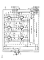
- FIG. 1 is a diagram showing a control block of a hybrid vehicle (hereinafter referred to as “HEV”).
- HEV hybrid vehicle
- Engine EGN and motor generator MG1 and motor generator MG2 generate vehicle running torque.
- Motor generator MG1 and motor generator MG2 not only generate rotational torque, but also have a function of converting mechanical energy externally applied to motor generator MG1 or motor generator MG2 into electric power.
- the motor generator MG1 or MG2 is, for example, a synchronous machine or an induction machine, and operates as a motor or a generator depending on the operation method as described above.
- a permanent magnet type synchronous motor using a magnet such as neodymium is suitable.
- the permanent magnet type synchronous motor generates less heat from the rotor than the induction motor, and is excellent for automobiles from this viewpoint.
- the output torque of the engine EGN and the output torque of the motor generator MG2 are transmitted to the motor generator MG1 via the power distribution mechanism TSM. It is transmitted to the wheel via the gear DEF.
- rotational torque is transmitted from the wheels to motor generator MG1, and AC power is generated based on the supplied rotational torque.
- the generated AC power is converted into DC power by the power conversion device 200 as described later, and the high-voltage battery 136 is charged, and the charged power is used again as travel energy.
- the electric power stored in the battery 136 for high voltage decreases, the rotational energy generated by the engine EGN is converted into AC power by the motor generator MG2, and then the AC power is converted into DC power by the power converter 200. And the battery 136 can be charged. Transmission of mechanical energy from engine EGN to motor generator MG2 is performed by power distribution mechanism TSM.
- the inverter circuits 140 and 142 are electrically connected to the battery 136 via the DC connector 138, and power is exchanged between the battery 136 and the inverter circuit 140 or 142.
- motor generator MG1 When motor generator MG1 is operated as a motor, inverter circuit 140 generates AC power based on DC power supplied from battery 136 via DC connector 138 and supplies it to motor generator MG1 via AC terminal 188.
- the configuration comprising motor generator MG1 and inverter circuit 140 operates as a first motor generator unit.
- inverter circuit 142 when motor generator MG2 is operated as a motor, inverter circuit 142 generates AC power based on the DC power supplied from battery 136 via DC connector 138, and is supplied to motor generator MG2 via AC terminal 159. Supply.
- the configuration composed of motor generator MG2 and inverter circuit 142 operates as a second motor generator unit.
- the first motor generator unit and the second motor generator unit may be operated as both motors or generators depending on the operating state, or may be operated using both of them. It is also possible to stop without driving one.
- the first motor generator unit is operated as the electric unit by the electric power of the battery 136, so that the vehicle can be driven only by the power of the motor generator MG1.
- the battery 136 can be charged by generating power by operating the first motor generator unit or the second motor generator unit as the power generation unit by the power of the engine 120 or the power from the wheels.
- the battery 136 is also used as a power source for driving an auxiliary motor 195.
- the auxiliary motor is, for example, a motor that drives a compressor of an air conditioner or a motor that drives a control hydraulic pump.
- DC power is supplied from the battery 136 to the auxiliary module 350, AC power is generated by the auxiliary module 350, and is supplied to the auxiliary motor 195 through the AC terminal 120.
- the auxiliary module 350 has basically the same circuit configuration and function as the inverter circuits 140 and 142, and controls the phase, frequency, and power of alternating current supplied to the auxiliary motor 195.
- the power conversion device 200 includes a capacitor module 500 for smoothing DC power supplied to the inverter circuit 140, the inverter circuit 142, and the inverter circuit 350B.
- the power conversion device 200 includes a communication connector 21 for receiving a command from a host control device or transmitting data representing a state to the host control device.
- the control circuit 172 calculates the control amount of the motor generator MG1, the motor generator MG2, and the auxiliary motor 195, and further calculates whether to operate as a motor or a generator.
- the control pulse is generated, and the control pulse is supplied to the driver circuit 174 and the driver circuit 350B of the accessory module 350.
- the auxiliary module 350 may have a dedicated control circuit. In this case, the dedicated control circuit generates a control pulse based on a command from the connector 21, and sends the control pulse to the driver circuit 350 B of the auxiliary module 350. Supply.
- the driver circuit 174 Based on the control pulse, the driver circuit 174 generates a drive pulse for controlling the inverter circuit 140 and the inverter circuit 142.
- the driver circuit 350A generates a control pulse for driving the inverter circuit 350B of the auxiliary module 350.
- the configuration of the electric circuit of the inverter circuit 140 and the inverter circuit 142 will be described with reference to FIG. Since the circuit configuration of the inverter 350B of the auxiliary module 350 shown in FIG. 1 is basically similar to the circuit configuration of the inverter circuit 140, the description of the specific circuit configuration of the inverter 350B is omitted in FIG. The inverter circuit 140 will be described as a representative example. However, since the auxiliary module 350 has low output power, the semiconductor chips constituting the upper arm and lower arm of each phase and the circuit connecting the chips described below are integrated into the auxiliary module 350. Has been placed.
- the inverter circuit 140 since the inverter circuit 140 and the inverter circuit 142 are very similar in circuit configuration and operation, the inverter circuit 140 will be described as a representative.
- the inverter circuit 140 includes a U-phase, a V-phase of AC power to be output from a series circuit 150 of upper and lower arms composed of an IGBT 328 and a diode 156 that operate as an upper arm, and an IGBT 330 and a diode 166 that operate as a lower arm.
- a series circuit 150 of upper and lower arms composed of an IGBT 328 and a diode 156 that operate as an upper arm
- an IGBT 330 and a diode 166 that operate as a lower arm.
- W phase corresponds to the three-phase windings of the armature winding of motor generator MG1.
- the series circuit 150 of the upper and lower arms of each of the three phases outputs an alternating current from an intermediate electrode 169 that is the middle point portion of the series circuit, and this alternating current passes through the alternating current terminal 159 and the alternating current connector 188 to the motor generator MG1.
- An AC power line is connected to AC bus bars 802 and 804 described below.
- the collector electrode 153 of the IGBT 328 in the upper arm is connected to the capacitor terminal 506 on the positive electrode side of the capacitor module 500 through the positive electrode terminal 157, and the emitter electrode of the IGBT 330 in the lower arm is connected to the capacitor terminal on the negative electrode side of the capacitor module 500 through the negative electrode terminal 158. 504 are electrically connected to each other.
- the control circuit 172 receives a control command from the host control device via the connector 21, and based on this, the IGBT 328 that configures the upper arm or the lower arm of each phase series circuit 150 that constitutes the inverter circuit 140. And a control pulse which is a control signal for controlling the IGBT 330 is generated and supplied to the driver circuit 174. Based on the control pulse, the driver circuit 174 supplies a drive pulse for controlling the IGBT 328 and the IGBT 330 constituting the upper arm or the lower arm of each phase series circuit 150 to the IGBT 328 and the IGBT 330 of each phase. IGBT 328 and IGBT 330 perform conduction or cutoff operation based on the drive pulse from driver circuit 174, convert DC power supplied from battery 136 into three-phase AC power, and supply the converted power to motor generator MG1. Is done.
- the IGBT 328 includes a collector electrode 153, a signal emitter electrode 155, and a gate electrode 154.
- the IGBT 330 includes a collector electrode 163, a signal emitter electrode 165, and a gate electrode 164.
- a diode 156 is electrically connected between the collector electrode 153 and the emitter electrode.
- a diode 166 is electrically connected between the collector electrode 163 and the emitter electrode.
- a metal oxide semiconductor field effect transistor hereinafter abbreviated as MOSFET
- MOSFET metal oxide semiconductor field effect transistor
- the capacitor module 500 includes a plurality of positive-side capacitor terminals 506, a plurality of negative-side capacitor terminals 504, a positive-side power terminal 509, and a negative-side power terminal 508.
- the high-voltage DC power from the battery 136 is supplied to the positive power supply terminal 509 and the negative power supply terminal 508 via the DC connector 138, and the plurality of positive capacitor terminals 506 and the plurality of capacitor terminals 506 of the capacitor module 500 are supplied.
- the electric power is supplied from the capacitor terminal 504 on the negative electrode side to the inverter circuit 140, the inverter circuit 142, and the auxiliary module 350.
- DC power converted from AC power by the inverter circuit 140 or the inverter circuit 142 is supplied to the capacitor module 500 from the capacitor terminal 506 on the positive electrode side or the capacitor terminal 504 on the negative electrode side, and the power supply terminal 509 on the positive electrode side or the negative electrode side.
- the power is supplied from the power terminal 508 to the battery 136 via the DC connector 138 and stored in the battery 136.
- the control circuit 172 includes a microcomputer (hereinafter referred to as “microcomputer”) for performing arithmetic processing on the switching timing of the IGBT 328 and the IGBT 330.
- microcomputer As input information to the microcomputer, there are a target torque value required for the motor generator MG1, a current value supplied from the upper and lower arm series circuit 150 to the motor generator MG1, and a magnetic pole position of the rotor of the motor generator MG1.
- the target torque value is based on a command signal output from a host controller (not shown).
- the current value is detected based on a detection signal from the current sensor 180.
- the magnetic pole position is detected based on a detection signal output from a rotating magnetic pole sensor (not shown) such as a resolver provided in the motor generator MG1.
- the current sensor 180 detects the current value of three phases, but the current value for two phases may be detected and the current for three phases may be obtained by calculation. .
- the microcomputer in the control circuit 172 calculates the d and q axis current command values of the motor generator MG1 based on the target torque value, and the calculated d and q axis current command values and the detected d and q
- the voltage command values for the d and q axes are calculated based on the difference from the current value of the axis, and the calculated voltage command values for the d and q axes are calculated based on the detected magnetic pole position. Convert to W phase voltage command value.
- the microcomputer generates a pulse-like modulated wave based on the comparison between the fundamental wave (sine wave) and the carrier wave (triangular wave) based on the voltage command values of the U-phase, V-phase, and W-phase, and the generated modulation
- the wave is output to the driver circuit 174 as a PWM (pulse width modulation) signal.
- the driver circuit 174 When driving the lower arm, the driver circuit 174 outputs a drive signal obtained by amplifying the PWM signal to the gate electrode of the corresponding IGBT 330 of the lower arm.
- the driver circuit 174 when driving the upper arm, the driver circuit 174 amplifies the PWM signal after shifting the level of the reference potential of the PWM signal to the level of the reference potential of the upper arm, and uses this as a drive signal as a corresponding upper arm.
- the driver circuit 174 amplifies the PWM signal after shifting the level of the reference potential of the PWM signal to the level of the reference potential of the upper arm, and uses this as a drive signal as a corresponding upper arm.
- control unit 170 performs abnormality detection (overcurrent, overvoltage, overtemperature, etc.) to protect the upper and lower arm series circuit 150. For this reason, sensing information is input to the control circuit 172. For example, information on the current flowing through the emitter electrodes of the IGBTs 328 and IGBTs 330 is input from the signal emitter electrode 155 and the signal emitter electrode 165 of each arm to the corresponding drive unit (IC). Thereby, each drive part (IC) detects an overcurrent, and when an overcurrent is detected, the switching operation of the corresponding IGBT 328 and IGBT 330 is stopped, and the corresponding IGBT 328 and IGBT 330 are protected from the overcurrent.
- abnormality detection overcurrent, overvoltage, overtemperature, etc.
- Information on the temperature of the upper and lower arm series circuit 150 is input to the microcomputer from a temperature sensor (not shown) provided in the upper and lower arm series circuit 150.
- voltage information on the DC positive side of the upper and lower arm series circuit 150 is input to the microcomputer.
- the microcomputer performs over-temperature detection and over-voltage detection based on the information, and stops switching operations of all the IGBTs 328 and IGBTs 330 when an over-temperature or over-voltage is detected.
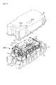
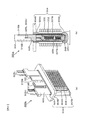
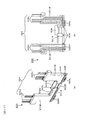
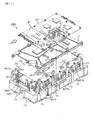
- FIG. 3 shows an exploded perspective view of a power conversion device 200 as an embodiment according to the present invention.
- the power conversion device 200 includes a housing 10 having a bottom made of aluminum and a lid 8 for storing circuit components of the power conversion device 200 fixed to the transmission TM. Since the power converter 200 has a substantially rectangular shape on the bottom and top surfaces, it can be easily attached to the vehicle and can be easily produced.
- the flow path forming body 12 holds a power semiconductor module 300 and a capacitor module 500, which will be described later, and cools them with a cooling medium. Further, the flow path forming body 12 is fixed to the housing 10, and an inlet pipe 13 and an outlet pipe 14 are provided at the bottom of the housing 10. Water as a cooling medium flows into the flow path forming body 12 from the inlet pipe 13 and flows out from the outlet pipe 14 after being used for cooling.
- the lid 8 houses a circuit component that attacks the power conversion device 200 and is fixed to the housing 10.
- a control circuit board 20 on which a control circuit 172 is mounted is disposed on the inside of the lid 8.
- the lid 8 is provided with a first opening 202 and a second opening 204 connected to the outside, and the connector 21 is connected to an external control device via the first opening 202 and provided on the control circuit board 20. Signal transmission is performed between the control circuit 172 and an external control device such as a host control device. Low voltage DC power for operating the control circuit in the power converter 200 is supplied from the connector 21.
- the second opening 204 is provided with a DC connector 138 for transmitting and receiving DC power to and from the battery 136, and a negative power line 510 and a positive electrode for supplying high voltage DC power into the power converter 200.
- the side power line 512 electrically connects the battery 136 and a DC connector 138 that transmits and receives DC power to the capacitor module 500 and the like.
- the connector 21, the negative power line 510 and the positive power line 512 are extended toward the bottom surface of the lid 8, the connector 21 protrudes from the first opening 202, and the tips of the negative power line 510 and the positive power line 512 are Projecting from the second opening 204 constitutes a terminal of the DC connector 138.
- the lid 8 is provided with a sealing member (not shown) around the first opening 202 and the second opening 204 on the inner wall thereof.
- the orientation of the mating surfaces of the terminals of the connector 21 and the like varies depending on the vehicle model. However, particularly when mounting on a small vehicle, the mating surface is selected from the viewpoint of size restrictions in the engine room and assembly. It is preferable to make it upward.
- the workability is improved by projecting toward the opposite side of the transmission TM.
- the connector 21 needs to be sealed from the outside atmosphere.
- the lid 8 is assembled to the connector 21 from above, the lid 8 is attached when the lid 8 is assembled to the housing 10. The seal member that comes into contact with the connector 21 can press the connector 21 and the airtightness is improved.
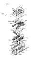
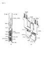
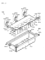
- FIG. 4 is an exploded perspective view for facilitating understanding of the configuration housed in the housing 10 of the power conversion device 200.
- a coolant channel 19 shown in FIG. 5 is formed in the channel forming body 12 along both sides.
- Openings 400 a to 400 c are formed on the upper surface on one side of the refrigerant flow path 19 along the refrigerant flow direction 418, and openings 402 a to 402 c are formed on the upper surface on the other side of the refrigerant flow path 19. It is formed along the flow direction 422 of the refrigerant.
- the openings 400a to 400c are closed by the inserted power semiconductor modules 300a to 300c, and the openings 402a to 402c are closed by the inserted power semiconductor modules 301a to 301c.
- a storage space 405 for storing the capacitor module 500 is formed between one and the other flow paths formed by the flow path forming body 12, and the capacitor module 500 is stored in the storage space 405. Thereby, the capacitor module 500 is cooled by the refrigerant flowing in the refrigerant flow path 19. Since the capacitor module 500 is sandwiched between the refrigerant flow path 19 for forming the refrigerant flow direction 418 and the refrigerant flow path 19 for forming the refrigerant flow direction 422, it can be efficiently cooled. Further, since the flow path for flowing the refrigerant along the outer surface of the capacitor module 500 is formed, the cooling efficiency is improved, and the arrangement of the refrigerant flow path, the capacitor module 500, and the power semiconductor modules 300 and 301 is neatly arranged.
- the coolant channel 19 is disposed along the long side of the capacitor module 500, and the distance between the coolant channel 19 and the power semiconductor modules 300 and 301 inserted and fixed in the coolant channel 19 is substantially constant.
- the circuit constants of the smoothing capacitor and the power semiconductor module circuit are easily balanced in each of the three-phase layers, and the circuit configuration is easy to reduce the spike voltage.
- water is most suitable as the refrigerant. However, since it can be used other than water, it will be referred to as a refrigerant hereinafter.
- the flow path forming body 12 is provided with a cooling unit 407 provided therein with a space for changing the flow of the refrigerant at a position facing the inlet pipe 13 and the outlet pipe 14.
- the cooling unit 407 is formed integrally with the flow path forming body 12 and is used for cooling the auxiliary device module 350 in this embodiment.
- the auxiliary module 350 is fixed to a cooling surface that is the outer peripheral surface of the cooling unit 407, stores the refrigerant in a space formed inside the cooling surface, and the cooling unit 407 is cooled by the refrigerant, whereby the auxiliary module 350 Temperature rise is suppressed.
- the refrigerant is a refrigerant flowing in the refrigerant flow path 19, and the auxiliary module 350 is cooled together with the power semiconductor modules 300 and 301 and the capacitor module 500.
- a bus bar assembly 800 described later is disposed on both sides of the accessory module 350.
- the bus bar assembly 800 includes an AC bus bar 186 and a holding member, and holds and fixes the current sensor 180. Details will be described later.
- the storage space 405 of the capacitor module 500 is provided in the center of the flow path forming body 12, the refrigerant flow paths 19 are provided so as to sandwich the storage space 405, and a power semiconductor for driving a vehicle is provided in each refrigerant flow path 19.
- the modules 300a to 300c and the power semiconductor modules 301a to 301c and further arranging the auxiliary module 350 on the upper surface of the flow path forming body 12 it is possible to efficiently cool in a small space, and to reduce the size of the entire power converter. Is possible.
- the refrigerant flow path 19 of the flow path forming body 12 by casting an aluminum material integrally with the flow path forming body 12, the refrigerant flow path 19 has the effect of increasing the mechanical strength in addition to the cooling effect. .
- the flow path forming body 12 and the refrigerant flow path 19 are integrated with each other by being made by aluminum casting, heat conduction is improved, and cooling efficiency is improved.
- the power semiconductor modules 300a to 300c and the power semiconductor modules 301a to 301c are fixed to the coolant channel 19 to complete the coolant channel 19, and a water leak test is performed. When the water leakage test is passed, the work of attaching the capacitor module 500, the auxiliary module 350, and the substrate can be performed next.
- the flow path forming body 12 is disposed at the bottom of the power conversion device 200, and then the work of fixing necessary components such as the capacitor module 500, the auxiliary module 350, the bus bar assembly 800, and the substrate is sequentially performed from the top. It is configured to be able to do so, improving productivity and reliability.
- the driver circuit board 22 is disposed above the auxiliary module 350 and the bus bar assembly 800, that is, on the lid side.
- a metal base plate 11 is disposed between the driver circuit board 22 and the control circuit board 20, and the metal base board 11 has a function of an electromagnetic shield of a circuit group mounted on the driver circuit board 22 and the control circuit board 20.
- the heat generated by the driver circuit board 22 and the control circuit board 20 is released and cooled. Further, it acts to increase the mechanical resonance frequency of the control circuit board 20. That is, it is possible to dispose screwing portions for fixing the control circuit board 20 to the metal base plate 11 at short intervals, shorten the distance between the support points when mechanical vibration occurs, and reduce the resonance frequency. Can be high. Since the resonance frequency of the control circuit board 20 can be increased with respect to the vibration frequency transmitted from the transmission, it is difficult to be affected by vibration and the reliability is improved.
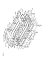
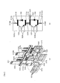
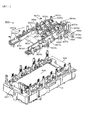
- FIG. 5 is an explanatory diagram for explaining the flow path forming body 12, and is a view of the flow path forming body 12 shown in FIG. 4 as viewed from below.
- the flow path forming body 12 and the refrigerant flow path 19 formed inside the flow path forming body 12 along the storage space 405 (see FIG. 4) of the capacitor module 500 are integrally cast.
- An opening 404 connected to one is formed on the lower surface of the flow path forming body 12, and the opening 404 is closed by a lower cover 420 having an opening at the center.
- a seal member 409a and a seal member 409b are provided between the lower cover 420 and the flow path forming body 12 to maintain airtightness.
- An inlet hole 401 for inserting the inlet pipe 13 (see FIG. 4) and the outlet pipe 14 (see FIG. 4) are inserted into the lower cover 420 in the vicinity of one end side and along the one side.
- An outlet hole 403 is formed.
- the lower cover 420 is formed with a convex portion 406 that protrudes in the arrangement direction of the transmission TM.
- the convex portion 406 is provided corresponding to the power semiconductor modules 300a to 300c and the power semiconductor modules 301a to 301c.
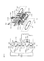
- the refrigerant flows in the direction of the flow direction 417 indicated by the dotted line through the inlet hole 401 toward the first flow path portion 19a formed along the short side of the flow path forming body 12.
- the first flow path portion 19a forms a space for changing the flow of the refrigerant, and collides with the inner surface of the cooling portion 407 in the space to change the flow direction. At the time of the collision, the cooling section 407 is deprived of heat. Then, the refrigerant flows through the second flow path portion 19 b formed along the side in the longitudinal direction of the flow path forming body 12 as in the flow direction 418. Further, the refrigerant flows through the third flow path portion 19 c formed along the short side of the flow path forming body 12 as in the flow direction 421. The third flow path portion 19c forms a folded flow path.
- the refrigerant flows through the fourth flow path portion 19 d formed along the longitudinal side of the flow path forming body 12 as in the flow direction 422.
- the fourth flow path portion 19d is provided at a position facing the second flow path portion 19b with the capacitor module 500 interposed therebetween.
- the refrigerant flows out to the outlet pipe 14 through the fifth flow path portion 19e and the outlet hole 403 formed along the short side of the flow path forming body 12 as in the flow direction 423.
- the first flow path portion 19a, the second flow path portion 19b, the third flow path portion 19c, the fourth flow path portion 19d, and the fifth flow path portion 19e are all formed larger in the depth direction than in the width direction.
- the power semiconductor modules 300a to 300c are inserted from the openings 400a to 400c formed on the upper surface side of the flow path forming body 12 (see FIG. 4) and stored in the storage space in the second flow path section 19b.
- An intermediate member 408a for preventing the flow of the refrigerant is formed between the storage space for the power semiconductor module 300a and the storage space for the power semiconductor module 300b.
- an intermediate member 408b is formed between the storage space for the power semiconductor module 300b and the storage space for the power semiconductor module 300c to prevent the flow of the refrigerant.
- the intermediate member 408a and the intermediate member 408b are formed such that their main surfaces are along the flow direction of the refrigerant.
- the fourth flow path portion 19d forms a storage space and an intermediate member for the power semiconductor modules 301a to 301c.
- the flow path forming body 12 is formed such that the opening 404 faces the openings 400a to 400c and 402a to 402c, the flow path forming body 12 is configured to be easily manufactured by aluminum casting.
- the lower cover 420 is provided with a support portion 410a and a support portion 410b for contacting the housing 10 and supporting the power converter 200.
- the support portion 410 a is provided close to one end side of the lower cover 420, and the support portion 410 b is provided close to the other end side of the lower cover 420.
- the support portion 410b is configured to support the resistor 450.
- the resistor 450 is for discharging electric charges charged in the capacitor cell in consideration of occupant protection and safety during maintenance.
- the resistor 450 is configured to continuously discharge high-voltage electricity. However, in the unlikely event that there is any abnormality in the resistor or discharge mechanism, consideration was given to minimize damage to the vehicle. Must be configured. In other words, when the resistor 450 is arranged around the power semiconductor module, the capacitor module, the driver circuit board, etc., there is a possibility that the resistor 450 spreads in the vicinity of the main component in the event that the resistor 450 has a problem such as heat generation or ignition. Can be considered.
- the power semiconductor modules 300a to 300c, the power semiconductor modules 301a to 301c, and the capacitor module 500 are disposed on the opposite side of the housing 10 housing the transmission TM with the flow path forming body 12 interposed therebetween, and
- the resistor 450 is disposed in a space between the flow path forming body 12 and the housing 10. Accordingly, the resistor 450 is disposed in the closed space surrounded by the flow path forming body 12 and the housing 10 formed of metal.
- the electric charge stored in the capacitor cell in the capacitor module 500 passes through the wiring passing through the side portion of the flow path forming body 12 by the switching operation of the switching means mounted on the driver circuit board 22 shown in FIG. Discharge is controlled by the resistor 450.
- the switching is controlled so as to discharge at high speed. Since the flow path forming body 12 is provided between the driver circuit board 22 that controls the discharge and the resistor 450, the driver circuit board 22 can be protected from the resistor 450. In addition, since the resistor 450 is fixed to the lower cover 420, the resistor 450 is provided in a position that is very close to the refrigerant flow path 19, so that abnormal heat generation of the resistor 450 can be suppressed.
- the power semiconductor modules 300a to 300c and the power semiconductor modules 301a to 301c used in the inverter circuit 140 and the inverter circuit 142 will be described with reference to FIGS.
- the power semiconductor modules 300a to 300c and the power semiconductor modules 301a to 301c all have the same structure, and the structure of the power semiconductor module 300a will be described as a representative. 6 to 10, the signal terminal 325U corresponds to the gate electrode 154 and the signal emitter electrode 155 disclosed in FIG. 2, and the signal terminal 325L corresponds to the gate electrode 164 and the emitter electrode 165 disclosed in FIG. To do.
- the DC positive terminal 315B is the same as the positive terminal 157 disclosed in FIG. 2, and the DC negative terminal 319B is the same as the negative terminal 158 disclosed in FIG.
- the AC terminal 321 is the same as the AC terminal 159 disclosed in FIG.
- FIG. 6A is a perspective view of the power semiconductor module 300a of the present embodiment.
- FIG. 6B is a cross-sectional view of the power semiconductor module 300a of this embodiment.
- the power semiconductor elements (IGBT 328, IGBT 330, diode 156, and diode 166) constituting the upper and lower arm series circuit 150 are, as shown in FIG. 7 to FIG. 9, provided by the conductor plate 315 or conductor plate 318, or the conductor plate 316 or conductor plate. By 319, it is fixed by being sandwiched from both sides.
- These conductor plates are assembled with an auxiliary molded body 600 formed by integrally molding signal wirings that are the signal terminals 325U and 325L.
- the conductor plate 315 and the like are sealed with the first sealing resin 348 with the heat dissipation surface exposed, and the insulating sheet 333 is thermocompression bonded to the heat dissipation surface.
- the module primary sealing body 302 sealed with the first sealing resin 348 is inserted into the module case 304 and sandwiched with the insulating sheet 333, and is thermocompression bonded to the inner surface of the module case 304 that is a CAN type cooler.
- the CAN-type cooler is a cylindrical cooler having an insertion port 306 on one surface and a bottom on the other surface.
- the module case 304 is made of an aluminum alloy material such as Al, AlSi, AlSiC, Al—C, etc., and is integrally formed without a joint.
- the module case 304 has a structure in which no opening other than the insertion port 306 is provided, and the outer periphery of the insertion port 306 is surrounded by a flange 304B. Further, as shown in FIG.
- the first heat radiating surface 307A and the second heat radiating surface 307B which are wider than the other surfaces, are arranged facing each other, and the opposing first heat radiating surface 307A and The three surfaces connecting the second heat radiating surface 307B constitute a surface sealed with a width narrower than the first heat radiating surface 307A and the second heat radiating surface 307B, and the insertion port 306 is formed on the surface of the other side.
- the shape of the module case 304 does not need to be an accurate rectangular parallelepiped, and the corner may form a curved surface as shown in FIG.
- the metallic case having such a shape By using the metallic case having such a shape, even when the module case 304 is inserted into the coolant channel 19 through which a coolant such as water or oil flows, a seal against the coolant can be secured by the flange 304B. It is possible to prevent the medium from entering the inside of the module case 304 with a simple configuration.
- the fins 305 are uniformly formed on the first heat radiation surface 307A and the second heat radiation surface 307B facing each other.
- a curved portion 304A having an extremely thin thickness is formed on the outer periphery of the first heat radiating surface 307A and the second heat radiating surface 307B. Since the curved portion 304A is extremely thin to such an extent that it can be easily deformed by pressurizing the fin 305, the productivity after the module primary sealing body 302 is inserted is improved.
- the gap remaining inside the module case 304 is filled with the second sealing resin 351. Further, as shown in FIGS. 8 and 9, a DC positive electrode wiring 315A and a DC negative electrode wiring 319A for electrical connection with the capacitor module 500 are provided, and a DC positive electrode terminal 315B (157) is provided at the tip thereof. DC negative terminal 319B (158) is formed. An AC wiring 320 for supplying AC power to the motor generator MG1 or 194 is provided, and an AC terminal 321 (159) is formed at the tip thereof.
- the DC positive electrode wiring 315A is integrally formed with the conductor plate 315
- the DC negative electrode wiring 319A is integrally formed with the conductor plate 319
- the AC wiring 320 is integrally formed with the conductor plate 316.
- the gap between the conductor plate and the inner wall of the module case 304 can be reduced, and the power semiconductor element The generated heat can be efficiently transmitted to the fins 305.
- the generation of thermal stress can be absorbed by the insulating sheet 333, which is favorable for use in a power conversion device for a vehicle having a large temperature change. .
- FIG. 7A is an internal cross-sectional view in which the module case 304, the insulating sheet 333, the first sealing resin 348, and the second sealing resin 351 are removed in order to help understanding.
- FIG. 7B is an internal perspective view.
- FIG. 8A is an exploded view for helping understanding of the structure of FIG.
- FIG. 8B is a circuit diagram of the power semiconductor module 300.
- FIG. 9A is a circuit diagram for explaining an inductance reduction effect
- FIG. 9B is a perspective view showing a current flow for explaining an inductance reduction effect.
- the direct current positive electrode side conductor plate 315 and the alternating current output side conductor plate 316 are arranged in substantially the same plane.
- the collector electrode of the IGBT 328 on the upper arm side and the cathode electrode of the diode 156 on the upper arm side are fixed.
- the collector electrode of the IGBT 330 on the lower arm side and the cathode electrode of the diode 166 on the lower arm side are fixed.
- the AC conductor plate 318 and the conductor plate 319 are arranged in substantially the same plane.
- the emitter electrode of the IGBT 328 on the upper arm side and the anode electrode of the diode 156 on the upper arm side are fixed.
- an emitter electrode of the IGBT 330 on the lower arm side and an anode electrode of the diode 166 on the lower arm side are fixed.
- Each power semiconductor element is fixed to an element fixing portion 322 provided on each conductor plate via a metal bonding material 160.
- the metal bonding material 160 is, for example, a low-temperature sintered bonding material including a solder material, a silver sheet, and fine metal particles.
- Each power semiconductor element has a flat plate-like structure, and each electrode of the power semiconductor element is formed on the front and back surfaces. As shown in FIG. 7A, each electrode of the power semiconductor element is sandwiched between the conductor plate 315 and the conductor plate 318, or the conductor plate 316 and the conductor plate 319. In other words, the conductor plate 315 and the conductor plate 318 are stacked so as to face each other substantially in parallel via the IGBT 328 and the diode 156. Similarly, the conductor plate 316 and the conductor plate 319 have a stacked arrangement facing each other substantially in parallel via the IGBT 330 and the diode 166. Further, the conductor plate 316 and the conductor plate 318 are connected via an intermediate electrode 329. By this connection, the upper arm circuit and the lower arm circuit are electrically connected to form an upper and lower arm series circuit.
- the direct current positive electrode wiring 315A and the direct current negative electrode wiring 319A have a shape extending substantially in parallel while facing each other through an auxiliary mold body 600 formed of a resin material.
- the signal terminal 325U and the signal terminal 325L are integrally formed with the auxiliary mold body 600 and extend in the same direction as the DC positive electrode wiring 315A and the DC negative electrode wiring 319A.
- As the resin material used for the auxiliary mold body 600 a thermosetting resin having an insulating property or a thermoplastic resin is suitable. Thereby, it is possible to secure insulation between the DC positive electrode wiring 315A, the DC negative electrode wiring 319A, the signal terminal 325U, and the signal terminal 325L, and high-density wiring is possible.
- the direct current positive electrode wiring 315A and the direct current negative electrode wiring 319A are arranged so as to face each other substantially in parallel, so that currents that instantaneously flow during the switching operation of the power semiconductor element face each other in the opposite direction. As a result, the magnetic fields produced by the currents cancel each other out, and this action can reduce the inductance.
- the lower arm side diode 166 is in a conductive state in a forward bias state.
- the diode 166 on the lower arm side is reversely biased, and a recovery current caused by carrier movement passes through the upper and lower arms.
- a recovery current 360 shown in FIG. 9B flows through each of the conductor plates 315, 316, 318, and 319.
- the recovery current 360 passes through the DC positive terminal 315B (157) disposed opposite to the DC negative terminal 319B (158), and is subsequently formed by the conductor plates 315, 316, 318, 319.
- the loop-shaped current path flows through a path close to the DC positive terminal 315B (157) side of the conductor plate 315 and passes through the IGBT 328 and the diode 156 as indicated by a dotted line.
- the loop-shaped current path flows through a path farther from the DC positive terminal 315B (157) side of the conductor plate 318 as shown by the solid line, and then farther from the DC positive terminal 315B (157) side of the conductor board 316 as shown by the dotted line.
- the path flows through the IGBT 330 and the diode 166.
- the loop-shaped current path flows along a path close to the DC negative electrode wiring 319A side of the conductor plate 319.
- the loop-shaped current path passes through a path closer to or farther from the DC positive terminal 315B (157) or the DC negative terminal 319B (158), thereby forming a current path closer to the loop shape. Is done.
- FIG. 10 (a) is a perspective view of the auxiliary mold body 600
- FIG. 10 (b) is a transparent view of the auxiliary mold body 600.
- the auxiliary mold body 600 has the signal conductor 324 integrated by insert molding.
- the signal conductor 324 receives the temperature information of the upper arm side gate electrode terminal 154 and the emitter electrode terminal 155, the upper arm side gate electrode terminal 164 and the emitter electrode terminal 165 (see FIG. 2), and the power semiconductor element.
- a terminal for transmission is included. In the description of this embodiment, these terminals are collectively referred to as signal terminals 325U and 325L.
- the signal conductor 324 forms signal terminals 325U and 325L at one end, and forms element-side signal terminals 326U and 326L at the other end.
- the element-side signal terminals 326U and 326L are connected to signal pads provided on the surface electrode of the power semiconductor element by, for example, wires.
- the first sealing portion 601A has a shape extending in a direction crossing the major axis of the shape of the DC positive electrode wiring 315A, the DC negative electrode wiring 319A, or the AC wiring 320 shown in FIG.
- the second sealing portion 601B has a shape extending in a direction substantially parallel to the major axis of the shape of the DC positive electrode wiring 315A, the DC negative electrode wiring 319A, or the AC wiring 320.
- the second sealing portion 601B includes a sealing portion for sealing the signal terminal 325U on the upper arm side and a sealing portion for sealing the signal terminal 325L on the lower arm side.
- the auxiliary mold body 600 is formed so that its length is longer than the entire length of the conductor plates 315 and 316 arranged side by side or the entire length of the conductor plates 319 and 320 arranged side by side. That is, the lengths of the conductor plates 315 and 316 arranged side by side or the lengths of the conductor plates 319 and 320 arranged side by side are within the range of the lateral length of the auxiliary mold body 600.
- the first sealing portion 601A has a hollow shape and forms a wiring fitting portion 602B for fitting the DC negative electrode wiring 319A into the hollow.
- the first sealing portion 601A has a hollow shape and forms a wiring fitting portion 602A for fitting the DC positive electrode wiring 315A into the hollow.
- the first sealing portion 601A is disposed on the side of the wiring fitting portion 602A, has a hollow shape, and further forms a wiring fitting portion 602C for fitting the AC wiring 320 into the hollow. .
- Each wiring is positioned by fitting each wiring to these wiring fitting portions 602A to 602C. Thereby, it becomes possible to perform the filling operation of the resin sealing material after firmly fixing each wiring, and the mass productivity is improved.
- the wiring insulation part 608 protrudes in a direction away from the first sealing part 601A from between the wiring fitting part 602A and the wiring fitting part 602B. Since the plate-shaped wiring insulating portion 608 is interposed between the DC positive electrode wiring 315A and the DC negative electrode wiring 319A, it is possible to arrange the wiring insulating portion 608 so as to reduce the inductance while ensuring insulation.
- the first sealing portion 601A is formed with a mold pressing surface 604 that comes into contact with a mold used for resin sealing, and the mold pressing surface 604 prevents resin leakage during resin sealing.
- a protruding portion 605 for preventing is formed around the outer periphery in the longitudinal direction of the first sealing portion 601.
- a plurality of protrusions 605 are provided to enhance the resin leakage prevention effect.
- the protrusions 605 are also provided in the wiring fitting portions 602A and the wiring fitting portions 602B, it is possible to prevent the resin sealing material from leaking around the DC positive electrode wiring 315A and the DC negative electrode wiring 319A.
- the material of the first sealing portion 601A, the second sealing portion 601B, and the protrusion 605 is a heat that can be expected to have high heat resistance in consideration of being installed in a mold of about 150 to 180 ° C.
- a liquid crystal polymer of a plastic resin, polybutylene terephthalate (PBT) or polyphenylene sulfide resin (PPS) is desirable.
- a plurality of through holes 606 shown in FIG. 10B are provided in the longitudinal direction on the side of the power semiconductor element in the short direction of the first sealing portion 601A.
- the first sealing resin 348 flows into the through-hole 606 and hardens, whereby an anchor effect is exerted, and the auxiliary mold body 600 is firmly held by the first sealing resin 348, and temperature changes and machine Even if stress is applied by mechanical vibration, both do not peel off. It is difficult to peel even if the shape is uneven instead of the through hole.
- a certain degree of effect can be obtained by applying a polyimide coating agent to the first sealing portion 601A or roughening the surface.
- the auxiliary mold body 600 supporting each wiring is inserted into a mold preheated to about 150 to 180 ° C.
- the auxiliary mold body 600, the DC positive electrode wiring 315A, the DC negative electrode wiring 319A, the AC wiring 320, the conductor plate 315, the conductor plate 316, the conductor plate 318, and the conductor plate 319 are firmly connected to each other.
- the second sealing portion 601B is formed to extend from the vicinity of the module case 304 to the vicinity of the driver circuit board 22.
- the switching control signal can be normally transmitted even when exposed to a high voltage.
- the DC positive wiring 315A, the DC negative wiring 319A, the AC wiring 320, the signal terminal 325U, and the signal terminal 325L protrude from the module case 304 in the same direction, electrical insulation can be ensured and reliability is ensured. it can.
- FIG. 11 is an exploded perspective view for explaining the internal structure of the capacitor module 500.
- the laminated conductor plate 501 is composed of a negative electrode conductor plate 505 and a positive electrode conductor plate 507 formed of a plate-like wide conductor, and an insulating sheet 517 sandwiched between the negative electrode conductor plate 505 and the positive electrode conductor plate 507. As described below, the laminated conductor plate 501 cancels the magnetic flux against the current flowing through the series circuit 150 of the upper and lower arms of each phase, so that the inductance of the current flowing through the series circuit 150 of the upper and lower arms is reduced. .
- the laminated conductor plate 501 has a substantially rectangular shape.
- the negative power supply terminal 508 and the positive power supply terminal 509 are formed so as to rise from one side of the laminated conductor plate 501 in the short direction, and are connected to the positive conductor plate 507 and the negative conductor plate 505, respectively. ing. DC power is supplied to the positive power supply terminal 509 and the negative power supply terminal 508 via the DC connector 138 as described with reference to FIG.
- the capacitor terminals 503a to 503c are formed corresponding to the positive terminal 157 (315B) and the negative terminal 158 (319B) of each power semiconductor module 300 in a state where the capacitor terminals 503a to 503c are raised from one side in the longitudinal direction of the multilayer conductor plate 501. Is done.
- the capacitor terminals 503d to 503f correspond to the positive electrode terminal 157 (315B) and the negative electrode terminal 158 (319B) of each power semiconductor module 301 in a state where the capacitor terminals 503d to 503f are raised from the other side in the longitudinal direction of the multilayer conductor plate 501. Formed.
- the capacitor terminals 503a to 503f are raised in a direction crossing the main surface of the laminated conductor plate 501.
- Capacitor terminals 503a to 503c are connected to power semiconductor modules 300a to 300c, respectively.
- Capacitor terminals 503d to 503f are connected to power semiconductor modules 301a to 301c, respectively.
- a part of the insulating sheet 517 is provided between the negative-side capacitor terminal 504a and the positive-side capacitor terminal 506a constituting the capacitor terminal 503a to ensure insulation. The same applies to the other capacitor terminals 503b to 503f.
- the negative electrode conductor plate 505, the positive electrode conductor plate 507, the battery negative electrode side terminal 508, the battery positive electrode side terminal 509, and the capacitor terminals 503a to 503f are composed of integrally formed metal plates, and the upper and lower arms This has the effect of reducing the inductance with respect to the current flowing through the series circuit 150.
- a plurality of capacitor cells 514 are provided on the inner side of the capacitor module 500 below the laminated conductor plate 501.
- eight capacitor cells 514 are arranged in a line along one side in the longitudinal direction of the laminated conductor plate 501, and another eight capacitor cells 514 are arranged in the other side in the longitudinal direction of the laminated conductor plate 501.
- a total of 16 capacitor cells are provided in a row along the sides.
- the capacitor cells 514 arranged along the respective sides in the longitudinal direction of the multilayer conductor plate 501 are arranged symmetrically with respect to the dotted line AA shown in FIG.
- the direct current smoothed by the capacitor cell 514 is supplied to the power semiconductor modules 300a to 300c and the power semiconductor modules 301a to 301c, the current balance between the capacitor terminals 503a to 503c and the capacitor terminals 503d to 503f And the inductance of the laminated conductor plate 501 can be reduced. Moreover, since it can prevent that an electric current flows locally in the laminated conductor board 501, a heat balance can be equalized and heat resistance can also be improved.
- each capacitor cell 514 can be uniformly cooled by the refrigerant.
- the current balance between the capacitor terminals 503a to 503c and the capacitor terminals 503d to 503f can be made uniform to reduce the inductance of the multilayer conductor plate 501, and the heat balance can be made uniform to improve heat resistance. Can do.
- the capacitor cell 514 is a unit structure of the power storage unit of the capacitor module 500, and is a film in which two films each having a metal such as aluminum deposited thereon are stacked and wound, and each of the two metals is used as a positive electrode and a negative electrode. Use a capacitor.
- the electrode of the capacitor cell 514 is manufactured by spraying a conductor such as tin, with the wound shaft surfaces serving as a positive electrode and a negative electrode, respectively.
- the capacitor case 502 includes a storage portion 511 for storing the capacitor cell 514, and the storage portion 511 has a substantially rectangular upper surface and lower surface shown in the drawing.
- the capacitor case 502 is provided with fixing means for fixing the capacitor module 500 to the flow path forming body 12, for example, holes 520a to 520h for allowing screws to pass therethrough.
- fixing means for fixing the capacitor module 500 to the flow path forming body 12, for example, holes 520a to 520h for allowing screws to pass therethrough.
- the bottom surface portion 513 of the storage portion 511 has a smooth concavo-convex shape or a corrugated shape so as to match the surface shape of the cylindrical capacitor cell 514.
- the capacitor case 502 is filled with a filler (not shown). Since the bottom surface portion 513 has a corrugated shape in accordance with the shape of the capacitor cell 514, the capacitor cell 514 can be prevented from being displaced from a predetermined position when the filler is filled in the capacitor case 502.
- the capacitor cell 514 generates heat due to the electric current resistance of the metal thin film and the inner conductor deposited on the inner film due to the ripple current at the time of switching. Therefore, in order to easily release the heat of the capacitor cell 514 through the capacitor case 502, the capacitor cell 514 is molded with a filler. Furthermore, the moisture resistance of the capacitor cell 514 can be improved by using a resin filler. In the present embodiment, the refrigerant flow path is provided along the longitudinal direction of the storage portion 511 of the capacitor module 500, so that the cooling efficiency is improved.
- the capacitor module 500 is disposed so that the side wall forming the side in the longitudinal direction of the storage portion 511 is sandwiched between the refrigerant flow paths 19, so that the capacitor module 500 can be cooled efficiently.
- the capacitor cell 514 is disposed so that one of the electrode surfaces of the capacitor cell 514 is opposed to the inner wall forming the side in the longitudinal direction of the storage portion 511. As a result, heat is easily transferred in the direction of the winding axis of the film, so that heat easily escapes to the capacitor case 502 via the electrode surface of the capacitor cell 514.
- FIG. 12 is an external perspective view in which a power semiconductor module, a capacitor module, and a bus bar assembly are assembled to the flow path forming body 12.
- FIG. 13 is an enlarged view of a portion A in FIG. 11, 12, and 13, the direct current positive terminal 315 ⁇ / b> B (157), the direct current negative terminal 319 ⁇ / b> B (158), the alternating current terminal 321 (159), and the second sealing portion 601 ⁇ / b> B are arranged on the lid side in the longitudinal direction of the housing 10. It extends toward.
- the area of the current path of the DC positive terminal 315B (157) and the DC negative terminal 319B (158) is much smaller than the area of the current path of the laminated conductor plate 501. Therefore, when the current flows from the laminated conductor plate 501 to the DC positive terminal 315B (157) and the DC negative terminal 319B (158), the area of the current path changes greatly. That is, the current concentrates on the DC positive terminal 315B (157) and the DC negative terminal 319B (158). Further, when the DC positive terminal 315B (157) and the DC negative terminal 319B (158) protrude in a direction crossing the laminated conductor plate 501, in other words, the DC positive terminal 315B (157) and the DC negative terminal 319B (158) are stacked. If the conductor plate 501 is in a twisted relationship, a new connection conductor is required, which may reduce productivity and increase costs.
- the negative electrode side capacitor terminal 504a has a rising portion rising from the laminated conductor plate 501, and has a connection portion 542 at the tip thereof.
- the positive-side capacitor terminal 506a has a rising portion that rises from the laminated conductor plate 501, and has a connection portion 545 at the tip thereof.
- the connecting portion 542 and the connecting portion 545 are connected so that the DC negative terminal 319B (158) and the DC positive terminal 315B (157) of the power semiconductor modules 300 and 301 are sandwiched therebetween.
- the capacitor terminals 504a and 506a form a laminated structure through the insulating sheet until just before the connection portions 542 and 545, the inductance of the wiring portion of the capacitor terminals 504a and 506a where current concentrates can be reduced. Furthermore, the tip of the DC negative terminal 319B (158) and the side of the connecting portion 542 are connected by welding, and similarly, the tip of the DC positive terminal 315B (157) and the side of the connecting portion 545 are connected by welding. . For this reason, productivity can be improved in addition to characteristic improvement by low inductance.
- the tip of the AC terminal 321 (159) of the power semiconductor module 300 or 301 is connected to the tip of the AC bus bar 802a by welding.
- a production facility for welding making the welding machine movable in a plurality of directions with respect to an object to be welded leads to a complicated production facility, which is not preferable from the viewpoint of productivity and cost. Therefore, in the present embodiment, the welding location of the AC terminal 321 (159) and the welding location of the DC negative electrode terminal 319B (158) are arranged in a straight line along the longitudinal side of the flow path forming body 12. Thereby, it is possible to perform a plurality of weldings while moving the welding machine in one direction, and productivity is improved.
- the plurality of power semiconductor modules 300a to 300c are arranged in a straight line along the side in the longitudinal direction of the flow path forming body 12. Thus, productivity can be further improved when welding the plurality of power semiconductor modules 300a to 300c.
- FIG. 14 is an exploded perspective view of the flow path forming body 12 and the bus bar assembly 800 assembled with the power semiconductor module and the capacitor module.
- FIG. 15 is an external perspective view of the bus bar assembly 800 excluding the holding member 803. 14 and 15, a bus bar assembly 800 includes a holding member 803 for holding and fixing the first and second AC bus bars arranged on both sides, and a first AC bus bar 802a provided on both sides. To 802f and second AC bus bars 804a to 804f.
- the bus bar assembly 800 is further provided with a current sensor 180 for detecting an alternating current flowing through first and second alternating current bus bars 802 and 804 provided on both sides.
- the first and second AC bus bars 802 and 804 provided on both sides are each made of a wide conductor, and the first AC bus bars 802a to 802f on both sides up to the installation location of the current sensor 180a or the current sensor 180b are:
- the wide surface is disposed so as to be substantially perpendicular to the main surface of the multilayer conductor plate 501 of the capacitor module 500.
- the first AC bus bars 802a to 802f are each bent at a substantially right angle before the through hole of the current sensor 180a or 180b, so that the wide surfaces of these AC bus bars are substantially parallel to the main surface of the laminated conductor plate 501. After passing through the holes of current sensor 180a and current sensor 180b, they are connected to second AC bus bars 804a to 804f.
- the second AC bus bars 804a to 804f have a wide surface substantially perpendicular to the main surface of the laminated conductor plate 501 of the capacitor module 500, that is, a state where the narrow surface of the AC bus bar faces the vertical direction of the power converter. is doing.
- the first AC bus bars 802a to 802f pass through the holes of the current sensor 180a and the current sensor 180b, and then are connected to the connection portions 805a to 805f (connection portions 805d to 805d) formed in the first AC bus bars 802a to 802f. 805f is not shown) and is connected to the second AC bus bars 804a to 804f.
- the second AC bus bars 804a to 804f are bent at substantially right angles toward the capacitor module 500 in the vicinity of the connection portions 805a to 805f.
- the main surfaces of the second AC bus bars 804a to 804f are formed so as to be substantially perpendicular to the main surface of the multilayer conductor plate 501 of the capacitor module 500.
- the second AC bus bars 804a to 804f extend from the vicinity of the current sensor 180a or the current sensor 180b toward one side 12a in the short direction of the flow path forming body 12 as shown in FIGS. It is extended and formed so as to cross the side 12a. That is, the second AC bus bars 804a to 804f are formed so as to cross the side 12a with the main surfaces of the plurality of second AC bus bars 804a to 804f facing each other.
- the AC bus bars 802a, 802b, 802d, and 802e are disposed on both sides along the refrigerant flow path disposed on both inner sides of the housing 10, the overall size of the apparatus can be reduced. Further, since the narrow surfaces of the wide conductors are arranged so as to face the vertical direction of the device, the space occupied by the first AC bus bar 802 and the second AC bus bar 804 can be reduced, and the overall size of the device can be reduced. . Furthermore, by projecting the plurality of AC bus bars from the one surface side of the flow path forming body 12, it is easy to route the wiring outside the power converter 200, and the productivity is improved.
- the first AC bus bars 802a to 802f, the current sensors 180a and 180b, and the second AC bus bars 804a to 804f are held and insulated by a holding member 803 made of resin.
- the holding member 803 By the holding member 803, the second AC bus bars 804a to 804f improve the insulation between the metal flow path forming body 12 and the housing 10.
- the bus bar assembly 800 has a structure that is fixed to the flow path forming body 12 by a holding member 803. Even if heat is transmitted to the housing 10 from the outside, the temperature rise of the flow path forming body 12 in which the flow path of the cooling medium is formed is suppressed. By fixing the bus bar assembly 800 to the flow path forming body 12, not only the temperature rise of the bus bar assembly 800 can be suppressed, but also the temperature increase of the current sensor 180 held in the bus bar assembly 800 can be suppressed.
- the current sensor 180 has heat-sensitive characteristics, and the reliability of the current sensors 180a and 180b can be improved by the above structure.
- the power conversion device when the power conversion device is fixed to the transmission as in this embodiment, not only the heat is transmitted from the transmission TM side to the housing 10, but also the heat is transmitted from the motor generator side via the second AC bus bars 804a to 804f. Is transmitted. These heats can be blocked by the flow path forming body 12, or the heat can be released to the refrigerant, the temperature rise of the current sensors 180a and 180b can be suppressed, and the reliability can be improved.
- the holding member 803 includes a support member 807a and a support member 807b for supporting the driver circuit board 22 shown in FIG.
- a plurality of support members 807a are provided and are formed along one side of the flow path forming body 12 in the longitudinal direction.
- a plurality of support members 807 b are provided and are formed side by side along the other side in the longitudinal direction of the flow path forming body 12. Screw holes for fixing the driver circuit board 22 are formed at the distal ends of the support member 807a and the support member 807b.
- the holding member 803 has a protruding portion 806a and a protruding portion 806b that extend upward from locations where the current sensor 180a and the current sensor 180b are disposed.
- the protrusion 806a and the protrusion 806b are configured to penetrate the current sensor 180a and the current sensor 180b, respectively.
- the current sensor 180 a and the current sensor 180 b include a signal line 182 a and a signal line 182 b that extend in the arrangement direction of the driver circuit board 22.
- the signal line 182a and the signal line 182b are joined to the wiring pattern of the driver circuit board 22 by solder.
- the holding member 803, the support members 807a and 807b, and the protrusions 806a and 806b are integrally formed of resin.
- the holding member 803 has a function of positioning the current sensor 180 and the driver circuit board 22, the assembly and solder connection work between the signal line 182a and the driver circuit board 22 is facilitated. Further, by providing the holding member 803 with a mechanism for holding the current sensor 180 and the driver circuit board 22, the number of components as the whole power conversion device can be reduced.
- the holding member 803 is provided with a support member 808 for indicating the vicinity of the center portion of the driver circuit board 22 to reduce the influence of vibration applied to the driver circuit board 22.
- the resonance frequency of the driver circuit board 22 can be made higher than the frequency of vibration transmitted from the transmission TM, and the transmission applied to the driver circuit board 22.
- the influence of TM vibration can be reduced.
- the holding member 803 of the bus bar assembly 800 is fixed to the flow path forming body 12 with screws.
- the holding member 803 is provided with a bracket 809 for fixing one end of the accessory module 350.
- the auxiliary module 350 is disposed in the cooling unit 407, whereby the other end of the auxiliary module 350 is fixed to the cooling unit 407. As a result, the influence of vibration applied to the accessory module 350 can be reduced, and the number of parts for fixing can be reduced.
- FIG. 16 is an external perspective view showing a state in which the power semiconductor module, the capacitor module, the bus bar assembly 800 and the auxiliary module 350 are assembled to the flow path forming body 12.
- the current sensor 180 may not be used as a sensor at a temperature of about 100 ° C. or higher.
- the environment in which it is used is extremely severe and may become high temperature, and it is one of the important issues to protect the current sensor 180 from heat.
- the current sensor 180a and the current sensor 180b are disposed on the opposite side of the transmission TM with the flow path forming body 12 interposed therebetween. Thereby, it is difficult for the heat generated by the transmission TM to be transmitted to the current sensor, and the temperature increase of the current sensor can be suppressed.
- the second AC bus bars 804a to 804f are formed so as to cross the third flow path 19c shown in FIG.
- the current sensor 180a and the current sensor 180b are disposed closer to the AC terminal 321 (159) of the power module than the portions of the second AC bus bars 804a to 804f crossing the third flow path portion 19c.
- the second AC bus bars 804a to 804f are indirectly cooled by the refrigerant, and heat transmitted from the AC bus bar to the current sensor and further to the semiconductor chip in the power module can be relieved, thereby improving the reliability.
- a flow direction 811 shown in FIG. 16 indicates a flow direction of the refrigerant flowing through the fourth flow path 19d shown in FIG.
- the flow direction 812 indicates the flow direction of the refrigerant flowing through the second flow path 19b shown in FIG.
- the projection parts of the current sensor 180a and the current sensor 180b are surrounded by the projection part of the refrigerant flow path 19. Be placed. This further protects the current sensor from heat from the transmission TM.
- FIG. 17 is a perspective view showing a state in which the control circuit board 20 and the metal base plate 11 are separated to help understanding.
- the current sensor 180 is disposed above the capacitor module 500.
- the driver circuit board 22 is disposed above the current sensor 180 of FIG. 16, and is further supported by support members 807a and 807b provided in the bus bar assembly 800 shown in FIG.
- the metal base plate 11 is disposed above the driver circuit board 22 and is supported by a plurality of support members 15 erected from the flow path forming body 12 in this embodiment.
- the control circuit board 20 is disposed above the metal base plate 11 and is fixed to the metal base plate 11.
- the current sensor 180, the driver circuit board 22, and the control circuit board 20 are hierarchically arranged in the height direction, and the control circuit board 20 is arranged at the farthest place from the high-power power semiconductor modules 300 and 301, switching is performed. Noise or the like can be prevented from being mixed. Furthermore, the metal base plate 11 is electrically connected to the flow path forming body 12 that is electrically connected to the ground. The metal base plate 11 reduces noise mixed from the driver circuit board 22 into the control circuit board 20.
- a wiring connector When a wiring connector is used to electrically connect the current sensor 180 and the driver circuit board 22, it is desirable to prevent the complexity of the connection process and connection errors.
- a first hole 24 and a second hole 26 that penetrate the driver circuit board 22 are formed in the driver circuit board 22.
- the signal hole 325U and the signal terminal 325L of the power semiconductor module 300 are inserted into the first hole 24, and the signal terminal 325U and the signal terminal 325L are joined to the wiring pattern of the driver circuit board 22 by soldering.
- the signal line 182 of the current sensor 180 is inserted into the second hole 26, and the signal line 182 is joined to the wiring pattern of the driver circuit board 22 by solder. Note that solder bonding is performed from the surface side of the driver circuit board 22 opposite to the surface facing the flow path forming body 12.
- productivity can be further improved by joining the signal terminal 325 of the power semiconductor module 300 and the signal line 182 of the current sensor 180 by soldering from the same direction. Further, by providing the driver circuit board 22 with the first hole 24 for penetrating the signal terminal 325 and the second hole 26 for penetrating the signal line 182, it is possible to reduce the risk of connection mistakes. .
- the driver circuit board 22 of the present embodiment has a drive circuit (not shown) such as a driver IC chip mounted on the side facing the flow path forming body 12.
- a drive circuit such as a driver IC chip mounted on the side facing the flow path forming body 12.
- the heat of solder bonding is suppressed from being transmitted to the driver IC chip or the like, and damage to the driver IC chip or the like due to solder bonding is prevented.
- a high-profile component such as a transformer mounted on the driver circuit board 22 is disposed in the space between the capacitor module 500 and the driver circuit board 22, the entire power conversion device 200 can be reduced in height. Is possible.
- the power semiconductor modules 300 and 301 inserted and fixed in the refrigerant flow path 19 are cooled by the refrigerant flowing in the refrigerant flow path 19 and the capacitor module 500 is cooled. Further, it is desirable to cool the auxiliary module 350 in order to suppress a temperature rise due to heat generation. Since the portion that can be cooled in the housing 10 is limited, a cooling method and a cooling structure are required.
- the heat dissipating surface formed by the metal base of the accessory module 350 is disposed so as to face the cooling unit 407 shown in FIG.
- the cooling unit 407 in FIG. 4 is provided to cool the auxiliary module 350.
- the back side of the cooling unit 407 is shown in FIG.
- a cross-sectional view of the cooling unit 407 is shown in FIG. 4, 5, and 19, the auxiliary module 350 is fixed so that the heat radiating surface thereof is in contact with the outer peripheral surface of the cooling unit 407. Since the cooling unit 407 is formed above the inlet pipe 13, the refrigerant flowing from below collides with the inner wall of the cooling unit 407 and can efficiently take heat from the auxiliary module 350.
- the refrigerant reservoir 19f on the inflow side is made larger than the refrigerant reservoir 19g on the outlet side.
- the auxiliary module 350 can be efficiently cooled.
- FIG. 18 is a cross-sectional view of the power conversion device 200 as viewed from the direction C on the surface indicated by the broken line B in FIG.
- the flange 304B provided in the module case 304 is pressed against the opening of the flow path of the flow path forming body 12, and the module case 304 is pressed against the flow path forming body 12, thereby improving the airtightness of the refrigerant flow path 19. Can do.
- the refrigerant in the refrigerant flow path 19 needs to flow through the region where the fins 305 are formed.
- the fin 305 is not formed in the lower part of the module case 304 in order to secure the space of the curved portion 304A.
- the lower cover 420 is formed so that the lower portion of the module case 304 is fitted into the recess 430 formed in the lower cover 420. Thereby, it can prevent that a refrigerant
- the power semiconductor modules 300 and 301 incorporate the series circuit 150 of the upper and lower arms shown in FIG. 2 to reduce the inductance.
- FIGS. 20 to 22 show embodiments in which the upper arm and the lower arm are configured by separate power semiconductor modules.
- FIG. 20 is a top view of a state in which a power semiconductor module in which the upper or lower arm is accommodated in the power semiconductor module is used and these power semiconductor modules are accommodated in the flow path forming body 12.
- the flow path forming body 12 has refrigerant flow paths formed on both sides along the long side as described in FIG. 5, and the upper arm semiconductor module 150A containing the upper arm and the lower arm are arranged.
- the stored lower arm semiconductor modules 150B are alternately inserted into the refrigerant flow path.
- the upper arm semiconductor module 150A includes the positive terminal 157 shown in FIG. 2, an AC terminal 169A for taking out an AC current, and terminals 154 and 155 for control.
- the lower arm semiconductor module 150B includes a negative electrode terminal 158, an AC terminal 169B for taking out an AC current, and terminals 154 and 155 for control.
- the capacitor module 500 is housed in the center of the flow path forming body 12 in the same manner as shown in FIG.
- the positive capacitor terminal 506 is connected to the positive terminal 157, and the negative capacitor terminal 504 is the negative electrode.
- the terminal 158 is connected.
- DC power is supplied from the battery 136 of FIG. 1 to the capacitor via the DC connector 138 to the positive power terminal 509 and the negative power terminal 508, and the capacitor module 500 is connected to the positive terminal 157 of the upper arm semiconductor module 150A.
- DC power is supplied to the negative terminal 158 of the arm semiconductor module 150B.
- the AC terminal 169A of the upper arm semiconductor module 150A is connected to the AC terminal 169B of the lower arm semiconductor module 150B, a series circuit 150 of upper and lower arms is formed.
- FIG. 21 is a diagram showing a connection relationship between the AC terminal 169A of the upper arm semiconductor module 150A, the AC terminal 169B of the lower arm semiconductor module 150B, and the bus bars 802a to 802c
- FIG. 22 is an AC terminal 169A of the upper arm semiconductor module 150A
- 4 is a diagram showing a connection relationship between an AC terminal 169B of the lower arm semiconductor module 150B and the bus bar assembly 800.
- FIG. 20 the AC terminal 169A of the upper arm semiconductor module 150A and the AC terminal 169B of the lower arm semiconductor module 150B are connected by AC bus bars 802a to 802f in FIGS.
- an AC terminal 169A and an AC terminal 169B are connected by an AC bus bar 802a.
- the AC bus bar 802a fulfills two functions of connecting the upper arm semiconductor module 150A and the lower arm semiconductor module 150B in series and extracting AC current from the series connection point.
- the AC bus bar 802b to the AC bus bar 802f respectively perform two functions of correspondingly connecting the upper arm semiconductor module 150A and the lower arm semiconductor module 150B and taking out an alternating current from the series connection point.
- FIG. 22 includes a holding member 803 for holding AC bus bars 802a to 802f.
- FIGS. 20 to 22 is the embodiment of FIGS. 3 to 5 and FIGS. 11 to 19 for cooling and assembling methods of the capacitor module 500, the power semiconductor module, the current sensor 180, and the bus bar assembly 800. And basically the same. Therefore, the solutions and effects of the problems described in the embodiments of FIGS. 3 to 5 and FIGS. 11 to 19 can be obtained similarly.
Abstract
The disclosed power conversion device is provided with: a metallic housing which has an internal storage space with a lid at one vertical end and a floor closing the other vertical end; a passage forming body which forms a refrigerant passage along the side area inside the housing on the floor side vertically; multiple power semiconductor modules housing semiconductor chips and disposed such that DC terminals and control terminals for controlling operation of the semiconductor chips protrude externally; a capacitor module which, disposed centrally relative to the refrigerant passage formed along the side of the housing, is provided with DC terminals; an AC busbar assembly disposed more to the lid side in the vertical direction of the housing than the capacitor module and the refrigerant passage; and a driver circuit disposed on the lid side in the vertical direction. In a state inserted into the refrigerant passage, each power semiconductor module is fixed to the passage forming body, and the AC busbar assembly has multiple AC busbars and multiple fixing units for fixing said assembly.
Description
本発明は直流電力を交流電力に変換しあるいは交流電力を直流電力に変換するために使用する電力変換装置に関する。
The present invention relates to a power converter used for converting DC power into AC power or converting AC power into DC power.
一般に電力変換装置は、直流電源から直流電力を受ける平滑用のコンデンサモジュールとコンデンサモジュールから直流電力を受けて交流電力を発生するインバータ回路とインバータ回路を制御するための制御回路を備えている。前記交流電力は例えばモータに供給され、供給された交流電力に応じてモータは回転トルクを発生する。前記モータは一般的には発電機としての機能を有しており、外部からモータに対して機械エネルギが供給されると、前記モータは供給される機械エネルギに基づいて交流電力を発生する。上記電力変換装置は交流電力を直流電力に変換する機能も備えている場合が多く、モータが発生する交流電力は直流電力に変換される。直流電力から交流電力への変換、あるいは交流電力から直流電力への変換は上記制御装置によって制御される。例えば上記モータが同期電動機の場合には、同期電動機の回転子の磁極位置に対する固定子が発生する回転磁界の位相を制御することにより、上記電力変換に係る制御を行うことができる。電力変換装置の一例は日本国特開2009-2192170号公報に開示されている。
Generally, a power converter includes a smoothing capacitor module that receives DC power from a DC power supply, an inverter circuit that receives DC power from the capacitor module and generates AC power, and a control circuit for controlling the inverter circuit. The AC power is supplied to, for example, a motor, and the motor generates rotational torque in accordance with the supplied AC power. The motor generally has a function as a generator. When mechanical energy is supplied to the motor from the outside, the motor generates AC power based on the supplied mechanical energy. The power conversion device often has a function of converting AC power to DC power, and AC power generated by the motor is converted to DC power. Conversion from DC power to AC power or conversion from AC power to DC power is controlled by the control device. For example, when the motor is a synchronous motor, the control related to the power conversion can be performed by controlling the phase of the rotating magnetic field generated by the stator with respect to the magnetic pole position of the rotor of the synchronous motor. An example of a power converter is disclosed in Japanese Patent Application Laid-Open No. 2009-2192170.
電力変換装置は、例えば自動車に搭載され、同じく自動車に搭載された二次電池から直流電力を受け、走行用の回転トルクを発生する電動機に供給するための交流電力を発生する。また車の回生制動運転時には制動力を発生するために電動機は走行エネルギに基づき交流電力を発生し、発生した交流電力は電力変換装置によって直流電力に変換され、上記二次電池に蓄電され、再び車両走行用などの電力として使用される。
The power conversion device is mounted on, for example, an automobile, receives direct current power from a secondary battery also mounted on the automobile, and generates alternating current power to be supplied to an electric motor that generates rotational torque for traveling. In addition, in order to generate braking force during regenerative braking operation of the car, the motor generates AC power based on the running energy, and the generated AC power is converted into DC power by the power converter, stored in the secondary battery, and again It is used as electric power for driving a vehicle.
環境対策などの観点から、モータを駆動するために直流電力を交流電力に変換する電力変換装置の重要性が益々増大している。電力変換装置に対してはさらなる小型化のニーズが大きい。つまり電力変換装置の容積に対する変換電力の比をより大きくすることが望まれている。
From the viewpoint of environmental measures and the like, the importance of power conversion devices that convert DC power into AC power for driving a motor is increasing. There is a great need for further miniaturization of power conversion devices. That is, it is desired to increase the ratio of the converted power to the volume of the power converter.
本発明の目的は、より小型化が可能な電力変換装置を提供することである。
An object of the present invention is to provide a power converter that can be further downsized.
本発明の第1の態様による電力変換装置は、内部に収納空間を有し、縦方向の一方側に蓋を有し、他方側が底によりふさがれている金属性のハウジングと、ハウジングの縦方向における底側であって、ハウジングの内部の側部に沿って冷媒流路を形成する流路形成体と、直流電力を交流電力に変換するインバータ回路を構成するための半導体チップを内蔵し、半導体チップに電流を流すための直流端子と半導体チップの動作を制御するための制御端子とが外部に突出するように設けられている複数のパワー半導体モジュールと、ハウジングの側部に沿って形成された冷媒流路に対して中央側に配置され、直流端子を備えたコンデンサモジュールと、コンデンサモジュールや冷媒流路より、ハウジングの縦方向における蓋側に配置された交流バスバーアッセンブリと、交流バスバーアッセンブリに対して、縦方向における蓋側に配置されたドライバ回路と、を有し、各パワー半導体モジュールは、冷媒流路に挿入された状態で流路形成体に固定され、交流バスバーアッセンブリは、各パワー半導体モジュールによって発生する交流電流を流すための複数の交流バスバーと該交流バスバーアッセンブリを固定するための複数の固定部とを有し、複数の交流バスバーは冷媒流路に沿って伸びる形状を成し、交流バスバーアッセンブリは複数の固定部によって固定されている。
本発明の第2の態様によると、第1の態様の電力変換装置において、コンデンサモジュールは略長方形の形状をなし、長方形の長辺に沿って冷媒流路が形成され、交流バスバーアッセンブリの複数の固定部は、冷媒流路に沿って配置されているのが好ましい。
本発明の第3の態様によると、第1の態様の電力変換装置において、コンデンサモジュールの外周に沿って冷媒流路が形成され、ドライバ回路はドライバ基板に形成されており、ドライバ基板は固定するための複数のドライバ固定部を有しており、ドライバ固定部は冷媒流路に沿って配置されているのが好ましい。
本発明の第4の態様による電力変換装置は、内部に収納空間を有し、縦方向の一方側に蓋を有し、他方側に底を有する金属性のハウジングと、ハウジングの縦方向における底側に冷媒流路を形成する流路形成体と、直流電力を交流電力に変換するインバータ回路を構成するための半導体チップを内蔵し、半導体チップに電流を流すための直流端子と交流電流を流すための交流端子と半導体チップの動作を制御するための制御端子とが外部に突出するように設けられている複数のパワー半導体モジュールと、冷媒流路に併設して配置され、直流端子を備えたコンデンサモジュールと、コンデンサモジュールや冷媒流路より、ハウジングの縦方向における蓋側に配置された交流バスバーアッセンブリと、パワー半導体モジュールの制御端子に半導体チップの制御信号を供給するドライバ回路と、有し、コンデンサモジュールの直流端子と各パワー半導体モジュールの直流端子とが電気的に接続され、交流バスバーアッセンブリは、冷媒流路に沿って伸びる幅広導体からなる複数の交流バスバーと該交流バスバーアッセンブリを固定するための複数の固定部とを有し、幅広導体からなる各交流バスバーは、それぞれ幅広導体の狭い面が縦方向を向き、幅広面が縦方向を横切る方向を向いていて、各交流バスバーの幅広面が空間を介して対向するように配置されており、交流バスバーアッセンブリの各交流バスバーは対応するパワー半導体モジュールの交流端子に接続されている。
本発明の第5の態様によると、第4の態様の電力変換装置において、交流バスバーアッセンブリより蓋側に、ドライバ回路を有する基板が配置され、パワー半導体モジュールの交流端子と対応する交流バスバーアッセンブリとが溶接により接続され、ドライバ回路を有する基板とパワー半導体モジュールの制御端子とが半田により接続されているのが好ましい。
本発明の第6の態様による電力変換装置は、内部に収納空間を有し、縦方向の一方側に蓋を、他方側に底を有する金属性のハウジングと、ハウジング内の底側であって、ハウジング内部の両側部のそれぞれに沿って、第1と第2の冷媒流路を形成する流路形成体と、直流電力を交流電力に変換するインバータ回路を構成するための半導体チップを内蔵し、半導体チップに電流を流すための直流端子と交流電流を流すための交流端子と半導体チップの動作を制御するための制御端子とが外部に突出するように設けられているパワー半導体モジュールと、第1と第2の冷媒流路に挟まれて配置され、直流端子を備えたコンデンサモジュールと、コンデンサモジュールや冷媒流路より、ハウジング内の蓋側に配置された交流バスバーアッセンブリと、パワー半導体モジュールの制御端子に制御信号を供給するドライバ回路と、を有し、第1と第2の冷媒流路にそれぞれ挿入されて、複数のパワー半導体モジュールが配置され、コンデンサモジュールの直流端子と対応するパワー半導体モジュールの直流端子とが電気的に接続され、交流バスバーアッセンブリは、第1と第2の冷媒流路に沿ってそれぞれ配置された、幅広形状の交流バスバーをそれぞれ複数有する第1と第2の交流バスバーの組と、該交流バスバーアッセンブリを固定するための複数の固定部とを有し、各交流バスバーの組は、幅広形状の交流バスバーのそれぞれの狭い面が縦方向を向き、幅広面が縦方向を横切る方向を向いて固定されており、第1の交流バスバーの組は第1の冷媒流路に沿って配置され、第2の交流バスバーの組は第2の冷媒流路に沿って配置され、第1と第2の交流バスバーの組の間に電気回路を配置した。
本発明の第7の態様によると、第6の態様の電力変換装置において、第1と第2の交流バスバーの組の間に配置された電気回路は補機用モータを駆動する交流電力を発生するための補機用のインバータ回路であるのが好ましい。
本発明の第8の態様による電力変換装置は、内部に収納空間を有する金属性のハウジングと、ハウジングの内部に配置され、直流端子を備えた平滑用のコンデンサモジュールと、コンデンサモジュールに沿って冷媒流路を形成する流路形成体と、直流電力を交流電力に変換するインバータ回路を構成するための上下アームの直列回路を内蔵し、上下アームの直列回路に電流を流すための直流端子と交流電力を出力するための交流端子と上下アームの動作を制御するための制御端子とが外部に突出するように設けられているパワー半導体モジュールと、コンデンサモジュールや冷媒流路より、ハウジングの縦方向における一方側に配置された交流バスバーアッセンブリと、交流バスバーアッセンブリに対してさらに縦方向の一方側に配置されたドライバ回路と、有し、冷媒流路に挿入されて複数のパワー半導体モジュールが配置され、コンデンサモジュールの直流端子からパワー半導体モジュールの直流端子に直流電力が供給されるように電気的に接続され、交流バスバーアッセンブリは、冷媒流路に沿って伸びる複数の幅広の交流バスバーと該交流バスバーアッセンブリを固定するための固定部とを有し、パワー半導体モジュールは、両面に冷却面を有し、縦方向に細長くしかも流路に沿って細長い形状をなす半導体モジュールケースと半導体モジュールケースから縦方向の一方側に突出する直流端子と交流端子とを有し、さらに直流端子や交流端子に対してさらに縦方向の一方側に長く突出する制御端子とが設けられており、交流バスバーアッセンブリは対応するパワー半導体モジュールの交流端子に電気的に接続され、ドライバ回路は対応するパワー半導体モジュールの制御端子に上アームあるいは下アームを制御するための制御信号を供給する。
本発明の第9の態様によると、第8の態様の電力変換装置であって、交流バスバーアッセンブリの幅広の交流バスバーはそれぞれ狭い面が縦方向となり、冷媒流路に沿ってそれぞれ伸びる形状をなしており、交流バスバーアッセンブリを構成する交流バスバーの幅広面が空間を介して互いに対向するように配置されているのが好ましい。
本発明の第10の態様によると、第8あるいは第9の内の一の態様の電力変換装置において、交流出力端は、冷媒流路に沿ってそれぞれ伸び方向に設けられているのが好ましい。
本発明の第11の態様による電力変換装置は、内部に収納空間を有する金属性のハウジングと、直流端子を備え、ハウジング内に設けられた平滑用のコンデンサモジュールと、ハウジング内においてコンデンサモジュールに沿うように冷媒流路を形成する流路形成体と、直流電力を交流電力に変換するインバータ回路を構成するための半導体チップを内蔵し、半導体チップに電流を流すための直流端子と交流電流を流すための交流端子と半導体チップの動作を制御するための制御端子とが外部に突出するように設けられているパワー半導体モジュールと、コンデンサモジュールや冷媒流路より、ハウジングの縦方向における一方側に配置された交流バスバーアッセンブリと、交流バスバーアッセンブリに対して、縦方向における一方側に配置されたドライバ回路と、を有し、コンデンサモジュールの直流端子と各パワー半導体モジュールの直流端子とが溶接によって接続され、交流バスバーアッセンブリは、冷媒流路に沿って伸びる複数の交流バスバーと該交流バスバーアッセンブリを固定するための固定部とを有し、該固定部によって交流バスバーアッセンブリが流路形成体に固定されている。
本発明の第12の態様によると、第11の態様の電力変換装置において、各パワー半導体モジュールの交流端子は対応するパワー半導体モジュールの交流端子と溶接により接続されているのが好ましい。
本発明の第13の態様による電力変換装置は、内部に収納空間を有し、縦方向の一方側に蓋を有し、他方側が底によりふさがれている金属性のハウジングと、ハウジングの内部の側部に沿って冷媒流路を形成する流路形成体と、直流電力を交流電力に変換するインバータ回路を構成するための半導体チップを内蔵し、半導体チップに電流を流すための直流端子と交流電流を流すための交流端子と半導体チップの動作を制御するための制御端子とが外部に突出するように設けらたパワー半導体モジュールと、冷媒流路に対して中央側に配置されて流路形成体に固定され、直流端子を備えたコンデンサモジュールと、コンデンサモジュールや冷媒流路より、ハウジングの縦方向における一方側に配置された交流バスバーアッセンブリと、ドライバ回路と、を有し、複数のパワー半導体モジュールが冷媒流路に挿入されて固定されており、交流バスバーアッセンブリは幅広の複数の交流バスバーと交流バスバーアッセンブリを固定するための固定部とを備えており、交流バスバーはそれぞれ幅の狭い面が縦方向を向いており、それぞれの幅広面が互いに空間を介して対向するように配置されており、固定部により交流バスバーアッセンブリが流路形成体に固定され、ドライバ回路が流路形成体に固定される。
本発明の第14の態様による電力変換装置は、内部に収納空間を有し、縦方向の一方側に蓋を有し、他方側が底によりふさがれている金属性のハウジングと、ハウジングの内部に配置され、ハウジングの側部に沿って冷媒流路を形成する流路形成体と、直流電力を交流電力に変換するインバータ回路を構成するための半導体チップを内蔵し、半導体チップに電流を流すための直流端子と交流電流を流すための交流端子と半導体チップの動作を制御するための制御端子とが外部に突出するように設けられ、冷媒流路に挿入されて固定されている複数のパワー半導体モジュールと、冷媒流路に対して中央側に配置されて流路形成体に固定され、直流端子を備えた平滑用のコンデンサモジュールと、コンデンサモジュールや冷媒流路より、ハウジングの縦方向における一方側に配置された交流バスバーアッセンブリと、パワー半導体モジュールの制御端子に制御信号を供給するドライバ回路と、を有し、コンデンサモジュールの直流端子は、コンデンサモジュールから突出して対応するパワー半導体モジュールの直流端子の方に伸び、その端部がパワー半導体モジュールの電流端子に沿って縦方向における一方側に伸びる形状をなし、コンデンサモジュールの直流端子の端部がパワー半導体モジュールの直流端子に溶接により接続され、交流バスバーアッセンブリが有する幅広形状をなす交流バスバーは、パワー半導体モジュールの交流端子の方に伸び、その端部が交流端子に沿って縦方向における一方側に伸びる形状を成し、端部が交流端子に溶接により接続され、ドライバ回路はパワー半導体モジュールの制御端子に半田により接続される。
本発明の第15の態様によると、第14の態様の電力変換装置において、コンデンサモジュールから突出して対応するパワー半導体モジュールの直流端子に接続される直流バスバーは、コンデンサモジュールからパワー半導体モジュールの電流端子の方にのびる第1の部分と、その端部が直流端子に沿って縦方向における一方側に伸びる第2の部分とを有し、第2の部分で溶接によりパワー半導体モジュールの直流端子に接続されており、交流バスバーアッセンブリが有する幅広導体の交流バスバーは、パワー半導体モジュールの交流端子の方にのびる第1の部分と、その端部が交流端子に沿って縦方向における一方側に折れ曲がって伸びる第2の部分とを有し、第2の部分で溶接によりパワー半導体モジュールの交流端子に接続されているのが好ましい。
本発明の第16の態様による電力変換装置は、内部に収納空間を有し、縦方向の一方側に蓋を有し、他方側が底により塞がれているとともに自動車用変速機に固定するための固定部を他方側の外部に有する金属性のハウジングと、金属性のハウジングの内部に配置され、冷媒を流すための冷媒流路を形成する流路形成体と、直流電力を交流電力に変換するためのインバータ回路を構成する半導体チップを内蔵するパワー半導体モジュールと、直流端子を有するコンデンサモジュールと、パワー半導体モジュールが発生する交流電流を流すための交流バスバーアッセンブリと、電流センサと、を有し、コンデンサモジュールに沿って冷媒流路が配置されるようにコンデンサモジュールと冷媒流路とを並べて配置し、交流バスバーアッセンブリはコンデンサモジュールに対して縦方向における一方側に配置され、交流バスバーアッセンブリは、交流電流を流すための複数の交流バスバーと、複数の交流バスバーを保持すると共に固定用の固定部を有する保持部材と、を備えており、交流バスバーアッセンブリは保持部材の固定部によって流路形成体に固定され、交流バスバーを流れる電流を計測するための電流センサを交流バスバーアッセンブリに固定した。
本発明の第17の態様による電力変換装置は、内部に収納空間を有し、縦方向の一方側に蓋を有し、他方側が底によりふさがれているとともに変速機に固定するための固定部を他方側の外部に有する金属性のハウジングと、金属性のハウジングの内部の両側部にそれぞれ冷媒を流すための冷媒流路を形成する流路形成体と、直流電力を交流電力に変換するパワー半導体モジュールと、平滑用のコンデンサモジュールとを配置し、コンデンサモジュールに対して、縦方向における一方側に交流電流を流すための交流バスバーアッセンブリを配置し、交流バスバーを流れる電流を計測するための電流センサを、コンデンサモジュールより、縦方向における一方側であって、冷媒を流す軸方向に対して、両側部に配置された冷媒流路によって挟まれる範囲内に、配置した。
本発明の第18の態様によると、第17の態様の電力変換装置において、交流バスバーアッセンブリはパワー半導体モジュールとコンデンサモジュールとに対して、縦方向における一方側に配置されており、交流バスバーアッセンブリはさらに流路形成体に固定され、流路形成体がハウジングに収納されているのが好ましい。 A power converter according to a first aspect of the present invention includes a metallic housing having a storage space therein, a lid on one side in the vertical direction, and the other side being blocked by the bottom, and the vertical direction of the housing Incorporates a semiconductor chip for forming a flow path forming body that forms a refrigerant flow path along the inner side of the housing, and an inverter circuit that converts DC power into AC power. A plurality of power semiconductor modules provided so that a direct current terminal for flowing current to the chip and a control terminal for controlling the operation of the semiconductor chip protrude to the outside, and formed along the side of the housing A capacitor module disposed on the center side with respect to the refrigerant flow path and having a DC terminal, and an AC buffer disposed on the lid side in the longitudinal direction of the housing from the capacitor module and the refrigerant flow path. And a driver circuit disposed on the lid side in the vertical direction with respect to the AC bus bar assembly, and each power semiconductor module is fixed to the flow path forming body in a state of being inserted into the refrigerant flow path. The AC bus bar assembly includes a plurality of AC bus bars for flowing an AC current generated by each power semiconductor module and a plurality of fixing portions for fixing the AC bus bar assembly. The AC bus bar assembly is fixed by a plurality of fixing portions.
According to the second aspect of the present invention, in the power conversion device according to the first aspect, the capacitor module has a substantially rectangular shape, a refrigerant flow path is formed along the long side of the rectangle, and a plurality of AC bus bar assemblies are provided. The fixing portion is preferably disposed along the refrigerant flow path.
According to the third aspect of the present invention, in the power conversion device of the first aspect, the refrigerant flow path is formed along the outer periphery of the capacitor module, the driver circuit is formed on the driver board, and the driver board is fixed. It is preferable that the driver fixing portion is disposed along the refrigerant flow path.
A power converter according to a fourth aspect of the present invention includes a metallic housing having a storage space inside, a lid on one side in the vertical direction, and a bottom on the other side, and a bottom in the vertical direction of the housing. A flow path forming body that forms a refrigerant flow path on the side and a semiconductor chip for configuring an inverter circuit that converts direct current power into alternating current power are built in, and a direct current terminal and an alternating current are passed through the semiconductor chip. A plurality of power semiconductor modules provided so that an AC terminal for controlling the operation of the semiconductor chip and a control terminal for controlling the operation of the semiconductor chip protrude to the outside, and a DC terminal provided with the refrigerant flow path The capacitor module, the AC bus bar assembly arranged on the lid side in the longitudinal direction of the housing from the capacitor module and the refrigerant flow path, and the control terminal of the power semiconductor module are semiconductive A driver circuit for supplying a chip control signal; and a DC terminal of the capacitor module and a DC terminal of each power semiconductor module are electrically connected, and the AC bus bar assembly is formed from a wide conductor extending along the refrigerant flow path. A plurality of AC bus bars and a plurality of fixing portions for fixing the AC bus bar assembly. Each AC bus bar made of a wide conductor has a narrow surface facing the vertical direction and a wide surface facing the vertical direction. The AC bus bars are arranged so that the wide surfaces of the AC bus bars face each other through a space, and each AC bus bar of the AC bus bar assembly is connected to the AC terminal of the corresponding power semiconductor module.
According to a fifth aspect of the present invention, in the power converter of the fourth aspect, the substrate having the driver circuit is disposed on the lid side of the AC bus bar assembly, and the AC bus bar assembly corresponding to the AC terminal of the power semiconductor module; Are connected by welding, and the substrate having the driver circuit and the control terminal of the power semiconductor module are preferably connected by solder.
A power conversion device according to a sixth aspect of the present invention includes a metallic housing having a storage space therein, a lid on one side in the vertical direction and a bottom on the other side, and a bottom side in the housing. A flow path forming body that forms first and second refrigerant flow paths and a semiconductor chip for constituting an inverter circuit that converts direct current power into alternating current power are incorporated along both sides of the housing. A power semiconductor module provided with a direct current terminal for flowing current to the semiconductor chip, an alternating current terminal for flowing alternating current, and a control terminal for controlling the operation of the semiconductor chip, A capacitor module disposed between the first and second refrigerant flow paths and having a DC terminal; and an AC bus bar assembly disposed closer to the lid in the housing than the capacitor module and the refrigerant flow path. A driver circuit that supplies a control signal to a control terminal of the power semiconductor module, and is inserted into the first and second refrigerant flow paths, respectively, and a plurality of power semiconductor modules are arranged, and a DC terminal of the capacitor module The DC bus terminals of the corresponding power semiconductor modules are electrically connected to each other, and the AC bus bar assembly includes first and second AC bus bars each having a plurality of wide shapes arranged along the first and second refrigerant flow paths. A set of second AC busbars and a plurality of fixing portions for fixing the AC busbar assembly; each AC busbar set is such that each narrow surface of the wide AC busbar faces in the vertical direction; The wide surface is fixed in a direction crossing the vertical direction, and the first set of AC bus bars is arranged along the first refrigerant flow path, and the second AC bus The set of chromatography are arranged along a second refrigerant flow path, the first and the electric circuit between the set of the second AC bus bars are arranged.
According to a seventh aspect of the present invention, in the power converter according to the sixth aspect, the electric circuit arranged between the first and second AC bus bar sets generates AC power for driving the auxiliary motor. It is preferable to use an inverter circuit for an auxiliary machine.
A power conversion device according to an eighth aspect of the present invention includes a metallic housing having a storage space therein, a smoothing capacitor module disposed inside the housing and having a DC terminal, and a refrigerant along the capacitor module. Built-in flow path forming body that forms a flow path and a series circuit of upper and lower arms for constructing an inverter circuit that converts DC power to AC power, and a DC terminal and AC for flowing current to the series circuit of the upper and lower arms A power semiconductor module provided so that an AC terminal for outputting electric power and a control terminal for controlling the operation of the upper and lower arms protrude to the outside, and a capacitor module and a refrigerant flow path in the vertical direction of the housing AC bus bar assembly arranged on one side and further arranged on one side in the vertical direction with respect to the AC bus bar assembly A plurality of power semiconductor modules, which are inserted into the refrigerant flow path, and are electrically connected so that DC power is supplied from the DC terminals of the capacitor module to the DC terminals of the power semiconductor module, The AC bus bar assembly has a plurality of wide AC bus bars extending along the refrigerant flow path and a fixing portion for fixing the AC bus bar assembly, and the power semiconductor module has a cooling surface on both sides, and has a longitudinal direction. A semiconductor module case that is elongated and has an elongated shape along the flow path, and a DC terminal and an AC terminal that protrude from the semiconductor module case to one side in the vertical direction, and further in the vertical direction with respect to the DC terminal and the AC terminal. A control terminal that protrudes long on one side of the AC bus bar assembly. Is electrically connected to the AC terminals of Yuru, it supplies a control signal for controlling the upper arm or the lower arm driver circuit to the control terminal of the corresponding power semiconductor module.
According to a ninth aspect of the present invention, in the power conversion device according to the eighth aspect, each of the wide AC bus bars of the AC bus bar assembly has a narrow surface in the vertical direction and a shape extending along the refrigerant flow path. It is preferable that the AC bus bars constituting the AC bus bar assembly are arranged so that the wide surfaces of the AC bus bars are opposed to each other through a space.
According to the tenth aspect of the present invention, in the power conversion device according to one of the eighth or ninth aspects, the AC output ends are preferably provided in the extending direction along the refrigerant flow path.
A power converter according to an eleventh aspect of the present invention includes a metallic housing having a storage space therein, a DC terminal, a smoothing capacitor module provided in the housing, and the capacitor module in the housing. In this way, a flow path forming body that forms a refrigerant flow path and a semiconductor chip for configuring an inverter circuit that converts direct current power into alternating current power are built in, and a direct current terminal and an alternating current are passed through the semiconductor chip. A power semiconductor module provided with an AC terminal for controlling the operation of the semiconductor chip and a control terminal for controlling the operation of the semiconductor chip, and a capacitor module and a coolant channel disposed on one side in the longitudinal direction of the housing Placed on one side in the vertical direction with respect to the AC bus bar assembly and the AC bus bar assembly A driver circuit, the DC terminal of the capacitor module and the DC terminal of each power semiconductor module are connected by welding, and the AC bus bar assembly includes a plurality of AC bus bars extending along the refrigerant flow path and the AC bus bar. A fixing portion for fixing the assembly, and the AC bus bar assembly is fixed to the flow path forming body by the fixing portion.
According to the twelfth aspect of the present invention, in the power conversion device according to the eleventh aspect, the AC terminal of each power semiconductor module is preferably connected to the AC terminal of the corresponding power semiconductor module by welding.
A power converter according to a thirteenth aspect of the present invention includes a metallic housing having a storage space inside, a lid on one side in the vertical direction, and the other side being blocked by the bottom, Built-in flow path forming body that forms a refrigerant flow path along the side and a semiconductor chip for configuring an inverter circuit that converts direct current power into alternating current power, and a direct current terminal for passing current through the semiconductor chip and alternating current A power semiconductor module provided with an AC terminal for supplying current and a control terminal for controlling the operation of the semiconductor chip protruding outside, and a flow path formed by being arranged on the center side with respect to the refrigerant flow path A capacitor module fixed to the body and provided with a DC terminal, an AC bus bar assembly disposed on one side of the housing in the longitudinal direction from the capacitor module and the refrigerant flow path, and a driver A plurality of power semiconductor modules are inserted and fixed in the refrigerant flow path, and the AC bus bar assembly includes a plurality of wide AC bus bars and a fixing portion for fixing the AC bus bar assembly. The AC bus bars are arranged such that the narrow surfaces face the vertical direction, and the wide surfaces face each other through a space, and the AC bus bar assembly is fixed to the flow path forming body by the fixing portion. Then, the driver circuit is fixed to the flow path forming body.
A power conversion device according to a fourteenth aspect of the present invention includes a metallic housing having a storage space therein, a lid on one side in the vertical direction, and the other side blocked by a bottom, and an interior of the housing. A flow path forming body that is disposed and forms a coolant flow path along the side of the housing, and a semiconductor chip for constituting an inverter circuit that converts DC power into AC power are built in, and a current flows through the semiconductor chip. A plurality of power semiconductors provided with a direct current terminal, an alternating current terminal for flowing an alternating current, and a control terminal for controlling the operation of the semiconductor chip so as to protrude to the outside and being inserted into the refrigerant flow path and fixed Module, a smoothing capacitor module which is disposed on the center side with respect to the refrigerant flow path and is fixed to the flow path forming body and having a DC terminal, and a capacitor module and the refrigerant flow path. An AC bus bar assembly disposed on one side of the power semiconductor module and a driver circuit for supplying a control signal to the control terminal of the power semiconductor module, the DC terminal of the capacitor module protruding from the capacitor module and corresponding power The DC terminal of the semiconductor module extends toward the DC terminal of the power semiconductor module, and the end of the DC terminal of the capacitor module extends to one side in the vertical direction along the current terminal of the power semiconductor module. The AC bus bar, which is connected by welding and has a wide shape that the AC bus bar assembly has, extends toward the AC terminal of the power semiconductor module, and its end extends along one side in the longitudinal direction along the AC terminal. The end is connected to the AC terminal by welding, and the driver circuit is powered It is connected by soldering to the control terminal of the semiconductor module.
According to the fifteenth aspect of the present invention, in the power conversion device of the fourteenth aspect, the DC bus bar protruding from the capacitor module and connected to the corresponding DC terminal of the power semiconductor module is connected to the current terminal of the power semiconductor module from the capacitor module. A first portion extending toward the end, and a second portion whose end extends to one side in the longitudinal direction along the DC terminal, and is connected to the DC terminal of the power semiconductor module by welding at the second portion The AC bus bar of the wide conductor included in the AC bus bar assembly extends in a first portion extending toward the AC terminal of the power semiconductor module and an end portion thereof bent along one side in the longitudinal direction along the AC terminal. A second portion, and connected to the AC terminal of the power semiconductor module by welding in the second portion. It is preferred.
A power conversion device according to a sixteenth aspect of the present invention has a storage space inside, a lid on one side in the vertical direction, and the other side closed by a bottom, and is fixed to an automobile transmission. A metallic housing having a fixed portion on the other side, a flow path forming body that is disposed inside the metallic housing and forms a refrigerant flow path for flowing a refrigerant, and converts DC power into AC power A power semiconductor module incorporating a semiconductor chip that constitutes an inverter circuit for performing the operation, a capacitor module having a DC terminal, an AC bus bar assembly for flowing an AC current generated by the power semiconductor module, and a current sensor. The capacitor module and the refrigerant channel are arranged side by side so that the refrigerant channel is arranged along the capacitor module. The AC bus bar assembly is disposed on one side in the longitudinal direction with respect to the capacitor module, and the AC bus bar assembly includes a plurality of AC bus bars for passing an AC current, a holding member that holds the plurality of AC bus bars and has a fixing portion for fixing, The AC bus bar assembly is fixed to the flow path forming body by the fixing portion of the holding member, and a current sensor for measuring the current flowing through the AC bus bar is fixed to the AC bus bar assembly.
A power conversion device according to a seventeenth aspect of the present invention has a storage space inside, a lid on one side in the vertical direction, the other side being blocked by the bottom, and a fixing portion for fixing to the transmission On the other side of the metallic housing, a flow passage forming body for forming a refrigerant flow passage for flowing the refrigerant to both sides of the inside of the metallic housing, and power for converting DC power to AC power A semiconductor module and a smoothing capacitor module are arranged. An AC bus bar assembly for flowing an alternating current is arranged on one side in the longitudinal direction with respect to the capacitor module, and a current for measuring the current flowing through the AC bus bar. The sensor is sandwiched between refrigerant flow paths disposed on both sides of the capacitor module on one side in the vertical direction and in the axial direction in which the refrigerant flows. Within the range, it was placed.
According to an eighteenth aspect of the present invention, in the power conversion device according to the seventeenth aspect, the AC bus bar assembly is arranged on one side in the longitudinal direction with respect to the power semiconductor module and the capacitor module, and the AC bus bar assembly is Further, it is preferable that the flow path forming body is fixed to the flow path forming body, and the flow path forming body is accommodated in the housing.
本発明の一実施の態様による電力変換装置は、電力変換装置のハウジングの内に、冷却媒体を流すための冷媒流路を形成する流路形成体と直流電力を交流電力に変換するインバータ回路を構成するための半導体チップを少なくとも1つ内蔵する複数のパワー半導体モジュールと平滑用のコンデンサモジュールとを備える。パワー半導体モジュールは半導体チップに電流を流すための直流端子やチップの動作を制御するための制御端子や交流電力を取り出す交流端子を有する。ハウジングの縦方向において、冷媒流路やコンデンサモジュールに対して空間を介して一方側に交流バスバーアッセンブリを配置し、交流バスバーアッセンブリのさらに一方側にドライバ回路を配置する。
A power converter according to an embodiment of the present invention includes a flow path forming body that forms a coolant flow path for flowing a cooling medium and an inverter circuit that converts DC power into AC power in a housing of the power converter. A plurality of power semiconductor modules incorporating at least one semiconductor chip for configuration and a smoothing capacitor module are provided. The power semiconductor module has a DC terminal for flowing current to the semiconductor chip, a control terminal for controlling the operation of the chip, and an AC terminal for taking out AC power. In the longitudinal direction of the housing, an AC bus bar assembly is disposed on one side of the refrigerant flow path and the capacitor module via a space, and a driver circuit is disposed on the other side of the AC bus bar assembly.
本発明によれば、電力変換装置の容積に対する変換電力の比をより大きくできる。
According to the present invention, the ratio of the converted power to the volume of the power converter can be increased.
以下に説明する本発明が適用された実施の形態に記載の電力変換装置およびこの装置を使用したシステムは、製品化のために解決することが望ましい色々な課題を解決している。これら実施の形態が解決している色々な課題の一つに、上述の発明が解決しようとする課題の欄に記載した小型化の課題があり、また上述の発明の効果の欄に記載した小型化の効果がある。すなわち以下に詳述する電力変換装置およびこの電力変換装置を使用したシステムは、製品化のために解決することが望ましい色々な課題を解決していて、上述の発明が解決しようとする課題の欄に記載した小型化の課題があり、また上述の発明の効果の欄に記載した小型化の効果に止まらず、上記課題や効果以外に色々な課題を解決し、色々な効果を達成することができる。さらに、上述の発明が解決しようとする課題の欄に記載した小型化の課題、また上述の発明の効果の欄に記載した小型化の効果を達成する構成についても、上述の課題を解決するための手段の欄に記載した構成だけで無く、他の構成によっても上記課題が解決でき、上記効果を得ることができる。すなわち小型化の課題や効果に関して上述した構成以外の構成によって、大きくは小型化に関する課題解決や効果達成につながるが、より具体的に見れば異なっている観点において課題が解決され、効果が得られている。以下その代表的なものを幾つか列挙する。さらにそれ以外については実施の形態の説明の中で述べる。
The power conversion device described in the embodiment to which the present invention described below is applied and a system using this device solve various problems that are desired to be solved for commercialization. One of the various problems solved by these embodiments is the problem of miniaturization described in the column of problems to be solved by the above-described invention, and the small size described in the column of effects of the above-mentioned invention. There is an effect. That is, the power conversion device described in detail below and the system using this power conversion device solve various problems that are desired to be solved for commercialization, and the above-described problems to be solved by the invention are described below. In addition to the above-described miniaturization effect described in the column of the effect of the invention, various problems other than the above-mentioned problems and effects can be solved and various effects can be achieved. it can. In order to solve the above-described problem, the configuration of achieving the miniaturization problem described in the column of the problem to be solved by the above-described invention and the effect of miniaturization described in the column of the effect of the above-mentioned invention are also achieved. The above problems can be solved and the above effects can be obtained not only by the configuration described in the column of means but also by other configurations. In other words, configurations other than those described above with regard to the issues and effects of miniaturization can lead to the solution and achievement of the issues related to miniaturization, but more specifically, the issues can be solved and the effects obtained from different viewpoints. ing. Some typical examples are listed below. Further, other matters will be described in the description of the embodiment.
より小型化が望ましい課題を解決するための構成1を次に記載する。構成1は、ハウジング内に、冷媒流路と平滑用のコンデンサモジュールを配置し、さらに前記冷媒流路に沿って縦長形状のパワー半導体モジュールを配置し、前記コンデンサモジュールから前記パワー半導体モジュールに直流電流を流すための直流バスバーを配置し、直流バスバーの縦方向における上側に交流バスバーを配置し、前記交流バスバーの上に前記パワー半導体モジュールを制御するための制御信号線を配置する構成である。この構成により、電力変換装置の全体構成をより整然とした状態で配置でき、電力変換装置の小型化が可能となる。また冷媒流路を横切る横方向における、すなわち、電力変換装置の横方向のサイズをより小さくできる効果を得ることができる。上記効果は特にインバータの上下のアームの直列回路を内蔵したパワー半導体モジュールを使用する場合に大きな効果が得られるが、上下のアームのどちらか1つのアームを挿入したパワー半導体モジュールを使用する場合であっても効果が達成できる。ただし、1つのアームを挿入したパワー半導体モジュールを使用する場合には、インバータの上アーム用と下用のパワー半導体モジュールを別々に使用するため、これらアーム接続するためのバスバー構成が増加する。
The configuration 1 for solving the problem that is desired to be smaller is described below. In the configuration 1, a refrigerant channel and a smoothing capacitor module are arranged in the housing, and a vertically long power semiconductor module is arranged along the refrigerant channel, and a direct current is passed from the capacitor module to the power semiconductor module. A DC bus bar for flowing the electric current, an AC bus bar on the upper side in the vertical direction of the DC bus bar, and a control signal line for controlling the power semiconductor module on the AC bus bar. With this configuration, the overall configuration of the power conversion device can be arranged in a more orderly manner, and the power conversion device can be downsized. Moreover, the effect which can make the size of the horizontal direction which crosses a refrigerant | coolant flow path, ie, the horizontal direction of a power converter device, smaller can be acquired. The above effect can be obtained particularly when using a power semiconductor module incorporating a series circuit of upper and lower arms of an inverter, but when using a power semiconductor module in which one of the upper and lower arms is inserted. Even if it is, the effect can be achieved. However, when a power semiconductor module into which one arm is inserted is used, the inverter upper arm and lower power semiconductor modules are used separately, and the bus bar configuration for connecting these arms increases.
上述の構成1において、さらにまた、直流バスバーや交流バスバーを電力変換装置のハウジング内のより側部側に配置し、これらバスバーの中央側に併設して前記コンデンサモジュールを配置でき、コンデンサモジュールの上部を有効に利用できる。例えばその他の回路をコンデンサモジュールの上部を配置でき、例えば実施の形態の如くコンプレッサなどの補機用の電動機を駆動する交流電力を発生するための補機用の半導体モジュールをこの部分に配置することができる。これらにより、電力変換装置の小型化を実現できる。さらに加えて、前記コンデンサモジュールとパワー半導体モジュールとの接続距離が短くなり、低インダクタンス化において効果がある。さらに溶接により電気的に接続する場合には、溶接器具を使用する空間が確保し易く、生産性が向上する。
In the configuration 1, the DC bus bar and the AC bus bar can be further arranged on the side of the side of the housing of the power converter, and the capacitor module can be arranged side by side on the center side of the bus bar. Can be used effectively. For example, other circuits can be arranged on the upper part of the capacitor module. For example, an auxiliary semiconductor module for generating AC power for driving an auxiliary electric motor such as a compressor is arranged in this portion as in the embodiment. Can do. As a result, the power converter can be downsized. In addition, the connection distance between the capacitor module and the power semiconductor module is shortened, which is effective in reducing the inductance. Furthermore, when electrically connecting by welding, it is easy to secure a space for using a welding instrument, and productivity is improved.
さらに上述の構成1において、コンデンサモジュールの外形に沿って冷媒流路を形成する流路形成体を設け、前記コンデンサモジュールを前記流路形成体に固定する構成とすることで、前記冷媒流路により前記パワー半導体モジュールと前記コンデンサモジュールとを合せて冷却できる。さらに直流バスバーや交流バスバーを側部の方に寄せて配置できるので、前記コンデンサモジュールの上側に配置した前記他の回路を流路形成体に接近して配置できる。前記パワー半導体モジュールと前記コンデンサモジュールとに加え、前記他の回路を効率的に冷却できる。前記他の回路とは回路を構成するためのいろいろな部品であっても良い。特に上述の通り、補機用の半導体モジュールを他の回路としてこの部分に配置することで、装置全体をより小型化でき、さらに補機用の半導体モジュールを効率的に冷却でき、信頼性の向上にもつながる。
Furthermore, in the above-described configuration 1, by providing a flow path forming body that forms a refrigerant flow path along the outer shape of the capacitor module and fixing the capacitor module to the flow path forming body, The power semiconductor module and the capacitor module can be cooled together. Furthermore, since the direct current bus bar and the alternating current bus bar can be arranged close to the side portion, the other circuit arranged on the upper side of the capacitor module can be arranged close to the flow path forming body. In addition to the power semiconductor module and the capacitor module, the other circuits can be efficiently cooled. The other circuit may be various parts for configuring the circuit. In particular, as described above, by placing the semiconductor module for auxiliary equipment in this part as another circuit, the entire device can be further miniaturized, and the semiconductor module for auxiliary equipment can be efficiently cooled, improving reliability. It also leads to.
より小型化が望ましいとの課題を解決するための他の構成である構成2を次に記載する。構成2は、パワー半導体モジュールから交流電力を出力するための、あるいはモータが発生した交流電力をパワー半導体モジュールに供給するための複数の交流バスバーを幅広の導体で構成し、各交流バスバーの幅の狭い面をハウジングの縦方向に沿うように、幅の広い面を互いに対向するように並べて配置したことである。この構成により、複数の交流バスバーが占める体積を小さくできる効果がある。
Next, Configuration 2 which is another configuration for solving the problem that smaller size is desirable is described below. In the configuration 2, a plurality of AC bus bars for outputting AC power from the power semiconductor module or supplying AC power generated by the motor to the power semiconductor module are configured by wide conductors, and the width of each AC bus bar That is, the narrow surfaces are arranged side by side along the longitudinal direction of the housing so that the wide surfaces face each other. With this configuration, there is an effect that the volume occupied by the plurality of AC bus bars can be reduced.
また上述の構成2に加え、上記複数の交流バスバーを交流バスバーアッセンブリとして一体化する構成とする。交流バスバーアッセンブリが、固定部を有する保持部材を有していて、前記保持部材に前記複数の交流バスバーを固定することにより前記複数の交流バスバーを一体化する構成とする。この構成により全体がより小型化できる。さらに交流バスバーアッセンブリの固定部を固定することで、前記複数の交流バスバーを固定でき、生産性が向上する。さらに他の回路やハウジング内面との緩衝の可能性も低減でき、信頼性の向上につながる。
In addition to the above-described configuration 2, the plurality of AC bus bars are integrated as an AC bus bar assembly. The AC bus bar assembly includes a holding member having a fixing portion, and the plurality of AC bus bars are integrated by fixing the plurality of AC bus bars to the holding member. With this configuration, the whole can be further downsized. Further, by fixing the fixing portion of the AC bus bar assembly, the plurality of AC bus bars can be fixed, and the productivity is improved. Furthermore, the possibility of buffering with other circuits and the inner surface of the housing can be reduced, leading to improved reliability.
また上述の構成2に加え、ハウジングの側部に沿って冷媒を流すための流路を配置し、前記冷媒の流路に沿って交流バスバーを配置するようにすれば、さらに電力変換装置の小型化の達成が容易と成る。また前記冷媒の流路に沿ってパワー半導体モジュールを配置することとなるので、電気的な接続も容易となる。
Further, in addition to the above-described configuration 2, if a flow path for flowing the refrigerant is arranged along the side of the housing and an AC bus bar is arranged along the flow path of the refrigerant, the power converter can be further reduced in size. It is easy to achieve the conversion. Further, since the power semiconductor module is disposed along the flow path of the refrigerant, electrical connection is facilitated.
より小型化が望ましいとの課題を解決するための他の構成である構成3を次に記載する。構成3は;パワー半導体モジュールから交流電力を出力するための、あるいはモータが発生した交流電力をパワー半導体モジュールが受けるための、複数の交流バスバーを幅広の導体で構成し;各交流バスバーを、ハウジングの両側部の方にそれぞれ配置された冷媒流に沿って配置し;両側部の前記交流バスバーに対してこれより中央の位置に、他の回路を配置したことである。他の回路としては、例えば実施の形態の如くコンプレッサなどの補機用の電動機を駆動する交流電力を発生するための補機用の半導体モジュールを配置することができる。これらにより、電力変換装置の小型化を実現できる。またこの効果に加え、補機用の半導体モジュールなどの他の回路を、冷媒流路を構成する流路形成他に直接あるいは接近して固定でき、パワー半導体モジュールに加え補機用の半導体モジュールなどの他の回路を効率良く冷却できる。
Next, Configuration 3, which is another configuration for solving the problem that smaller size is desirable, is described below. In the configuration 3, a plurality of AC bus bars for outputting AC power from the power semiconductor module or for receiving the AC power generated by the motor by the power semiconductor module are configured by wide conductors; It arrange | positions along the refrigerant | coolant flow each arrange | positioned toward the both sides of this; it is having arrange | positioned another circuit in the center position from this with respect to the said alternating current bus bar of both sides. As another circuit, for example, an auxiliary semiconductor module for generating AC power for driving an auxiliary electric motor such as a compressor can be disposed as in the embodiment. As a result, the power converter can be downsized. In addition to this effect, other circuits such as auxiliary semiconductor modules can be fixed directly or close to the flow path forming the refrigerant flow path, etc., in addition to power semiconductor modules, auxiliary semiconductor modules, etc. The other circuits can be efficiently cooled.
より小型化が望ましいとの課題を解決するための他の構成である構成4を次に記載する。構成4は;冷媒の流路に沿って配置したパワー半導体モジュールから突出する信号端子の接続位置を直流端子や交流端子より、縦方向のより一方側の方の位置に設け;前記縦方向において、コンデンサモジュールや交流バスバーよりドライバ回路を縦方向においてより一方側の位置に配置したことである。このような構成とすることで、大電流を流す直流や交流バスバーを配置する位置と前記信号端子に信号を供給する配線の位置とを、縦方向において分けることができ、配線を整理して配置できる。このことは電力変換装置の小型化の実現につながる。さらに大電流を流す直流や交流バスバーを溶接接続工程により接続し、前記信号端子の接続を半田接続工程で行う場合に、溶接工程と半田工程とを分けることができ、生産性の向上につながる。
Next, Configuration 4, which is another configuration for solving the problem that miniaturization is desirable, is described below. Configuration 4 is: providing a connection position of a signal terminal protruding from a power semiconductor module arranged along the flow path of the refrigerant at a position on one side of the vertical direction from the DC terminal or the AC terminal; That is, the driver circuit is arranged at one position in the vertical direction from the capacitor module or the AC bus bar. By adopting such a configuration, it is possible to divide the position in which the direct current or alternating current bus bar for supplying a large current is arranged and the position of the wiring for supplying a signal to the signal terminal in the vertical direction. it can. This leads to a reduction in the size of the power converter. Further, when a direct current or an alternating current bus bar for flowing a large current is connected by a welding connection process and the signal terminals are connected by a solder connection process, the welding process and the solder process can be separated, leading to an improvement in productivity.
より小型化が望ましいとの課題を解決するための他の構成である構成5を次に記載する。構成5は、電力変換装置を略直方体の構造とし、その上面の四角形の長辺側に沿って冷媒を流す冷媒流路を配置し、冷媒の流路に沿ってパワー半導体モジュールを配置し、さらに交流バスバーを幅広導体で構成すると共に、各交流導体の幅の狭い面を縦方向に、幅広面が互いに対向するようにして前記冷媒の流路に沿って伸びるように配置し、これら冷媒流路に沿って伸びる交流バスバーを前記電力変換装置の略四角形の短辺側に揃え、この短辺から交流電力を出力する構造としたことである。このような構造とすることで、交流バスバーの占める空間を小さくでき、また他の回路との配置関係が整い、電力変換装置をより小型にすることが可能となる。
Next, Configuration 5 which is another configuration for solving the problem that smaller size is desirable will be described. In the configuration 5, the power conversion device has a substantially rectangular parallelepiped structure, a refrigerant flow path for flowing the refrigerant along the long side of the quadrangle on the upper surface thereof, a power semiconductor module disposed along the flow path of the refrigerant, The AC bus bar is composed of wide conductors, and the AC conductors are arranged so that the narrow surfaces of the AC conductors extend in the vertical direction and extend along the refrigerant flow path so that the wide surfaces face each other. The AC bus bars extending along the line are arranged on the short side of the substantially square shape of the power converter, and the AC power is output from the short side. With such a structure, the space occupied by the AC bus bar can be reduced, the arrangement relationship with other circuits can be adjusted, and the power conversion device can be made smaller.
生産性の向上に係る課題を解決するための構成6を次に記載する。構成6は、電力変換装置のハウジングの内部に冷媒流路を形成するための冷媒流路形成体にコンデンサモジュールやパワー半導体モジュールを固定し、さらにその上に交流バスバーアッセンブリを配置する構造としている。このような構造とすることで、コンデンサモジュールとパワー半導体モジュールとの接続を容易に行うことができ、次にパワー半導体モジュールと交流バスバーアッセンブリとの接続を容易に行うことができる。このことにより、生産性が向上する。特にコンデンサモジュールとパワー半導体モジュールとの接続部には大電流が流れるため、溶接により電気的な接続を行うことが多い。先ずコンデンサモジュールとパワー半導体モジュールとを溶接により接続し、次に交流バスバーアッセンブリを固定してパワー半導体モジュールと交流バスバーアッセンブリとを溶接により接続することが可能となる。溶接による接続では溶接の器具を溶接部分に導くことが必要となり、上記の構造では、溶接器具を溶接部分に導くことが可能となる。また先に溶接による接続を行い、次に半田による接続を行うことで、作業性が向上する。上記構造は小型化に寄与するだけでなく、溶接工程により電気的な接続を行う場合には、生産性が向上する。さらにコンデンサモジュールとパワー半導体モジュールとの電気的な接続やパワー半導体モジュールと交流バスバーアッセンブリとの電気的な接続に溶接工程を使用することで、パワー半導体モジュールの端子部分にねじ止めのための面積を確保することが不要となり、パワー半導体モジュールをより小型にでき、このことは電力変換装置の小型化につながる。
The configuration 6 for solving the problem related to the improvement of productivity is described below. Configuration 6 has a structure in which a capacitor module and a power semiconductor module are fixed to a coolant channel forming body for forming a coolant channel inside the housing of the power conversion device, and an AC bus bar assembly is further disposed thereon. With such a structure, the capacitor module and the power semiconductor module can be easily connected, and then the power semiconductor module and the AC bus bar assembly can be easily connected. This improves productivity. In particular, since a large current flows through the connection portion between the capacitor module and the power semiconductor module, electrical connection is often performed by welding. First, the capacitor module and the power semiconductor module are connected by welding, and then the AC bus bar assembly is fixed and the power semiconductor module and the AC bus bar assembly can be connected by welding. In the connection by welding, it is necessary to guide the welding tool to the welded portion, and in the above structure, the welding tool can be guided to the welded portion. Also, workability is improved by performing connection by welding first and then by soldering. The above structure not only contributes to downsizing, but also improves productivity when electrical connection is made by a welding process. Furthermore, by using a welding process for electrical connection between the capacitor module and the power semiconductor module and between the power semiconductor module and the AC bus bar assembly, the terminal area of the power semiconductor module can be screwed. It is not necessary to secure the power semiconductor module, and the power semiconductor module can be made smaller, which leads to a reduction in the size of the power conversion device.
生産性の向上に係る課題を解決するための他の構成7を次に記載する。構成7は;上述の構成4で説明した構成と基本的に同じであり;冷媒の流路に沿って配置したパワー半導体モジュールから突出する信号端子の接続部を直流端子や交流端子の接続部より、縦方向のより一方側の方に配置し;前記縦方向において、コンデンサモジュールや交流バスバーよりドライバ回路を縦方向におけるより一方側の方に配置したことである。このような構成とすることで、大電流を流すバスバーを配置する位置と前記信号端子に信号を供給する配線の位置とを、縦方向において分け配置することで、縦方向に順に組み立てることができ、さらに縦方向に順に接続作業を行うことができる。このことにより、生産性が向上する。
Other configuration 7 for solving the problem related to the improvement of productivity is described below. Configuration 7 is basically the same as the configuration described in Configuration 4 above; the connection portion of the signal terminal protruding from the power semiconductor module arranged along the flow path of the refrigerant is connected to the connection portion of the DC terminal or AC terminal. In the vertical direction, the driver circuit is arranged on the one side of the vertical direction from the capacitor module and the AC bus bar. By adopting such a configuration, it is possible to assemble in order in the vertical direction by separately arranging the position in which the bus bar for supplying a large current and the position of the wiring for supplying a signal to the signal terminal are arranged in the vertical direction. In addition, connection work can be performed in order in the vertical direction. This improves productivity.
上記構成7においてさらに、大電流を流すバスバーに関係する電気的な接続を溶接接続により行い、信号端子に関する配線の接続を半田接続により行うことで、溶接工程を半田工程と分け、直流バスバーの溶接工程と交流バスバーの溶接工程とを近づけて行うことができる。このことにより、生産性が向上する。
In the configuration 7, the electrical connection related to the bus bar through which a large current flows is made by welding connection, and the wiring related to the signal terminal is made by solder connection, so that the welding process is separated from the solder process, and the welding of the DC bus bar is performed. The process and the welding process of the AC bus bar can be performed close to each other. This improves productivity.
信頼性の向上に係る課題を解決するための構成8を次に記載する。構成8は;金属性のハウジング内に、冷媒を流すための冷媒流路を形成する流路形成体を配置し;前記流路形成体に交流電流を流すための交流バスバーを固定し;前記交流バスバーを流れる電流を検出するための電流センサをバスバーに固定する構造である。前記流路形成体に固定されるバスバーに電流センサを配置することで、冷媒により冷却された流路形成体を介して交流バスバーを冷却し、モータ側から伝達される熱による交流バスバーの温度上昇を押さえ、電流センサの温度上昇を抑えることができる。
The configuration 8 for solving the problem related to the improvement of reliability is described below. Configuration 8 is: a flow path forming body for forming a refrigerant flow path for flowing a refrigerant is disposed in a metallic housing; an AC bus bar for flowing an alternating current is fixed to the flow path forming body; In this structure, a current sensor for detecting a current flowing through the bus bar is fixed to the bus bar. By arranging a current sensor on the bus bar fixed to the flow path forming body, the AC bus bar is cooled via the flow path forming body cooled by the refrigerant, and the temperature of the AC bus bar rises due to heat transmitted from the motor side. The temperature rise of the current sensor can be suppressed.
例えば、電力変換装置を車両のトランスミッションの如く高温度になる可能性の有る部材に固定する場合には、ハウジングを介して熱が伝達されてくる。またモータに交流電力を供給する交流バスバーは材料が銅であるため、良好な熱伝導体である。このためモータの熱が交流バスバーを介して伝えられ、電流センサの温度を高める可能性がある。構成8では、冷媒流路を形成する前記流路形成体に交流バスバーを固定し、前記交流バスバーに電流センサを固定したので、電流センサの温度上昇を抑制でき、信頼性が向上する。
For example, when the power conversion device is fixed to a member that has a high temperature, such as a transmission of a vehicle, heat is transmitted through the housing. An AC bus bar that supplies AC power to the motor is a good heat conductor because the material is copper. For this reason, the heat of the motor is transmitted through the AC bus bar, and the temperature of the current sensor may be increased. In Configuration 8, since the AC bus bar is fixed to the flow path forming body that forms the refrigerant flow path, and the current sensor is fixed to the AC bus bar, the temperature increase of the current sensor can be suppressed, and the reliability is improved.
信頼性の向上に係る課題を解決するための他の構成9を次に記載する。構成9は、上述の構成8において、固定部材および保持部材を有する交流バスバーアッセンブリを設け、この交流バスバーアッセンブリの前記保持部材により、前記交流バスバーを保持し固定する構成である。交流バスバーアッセンブリの固定手段により交流バスバーアッセンブリを前記流路形成体に固定する構成としている。交流バスバーアッセンブリ自身は上記固定部材により前記流路形成体に固定される。
Other configuration 9 for solving the problem related to the improvement of reliability is described below. A configuration 9 is a configuration in which the AC bus bar assembly having the fixing member and the holding member is provided in the configuration 8 described above, and the AC bus bar is held and fixed by the holding member of the AC bus bar assembly. The AC bus bar assembly is fixed to the flow path forming body by the fixing means of the AC bus bar assembly. The AC bus bar assembly itself is fixed to the flow path forming body by the fixing member.
この構成により交流バスバーアッセンブリの組み付けが容易と成ると共に、交流バスバーアッセンブリを前記流路形成体により冷却することができる。交流バスバーを効率的に冷却することができる。電流センサの温度上昇を抑制できるので電流センサ信頼性および電力変換装置全体の信頼性が向上する。電流センサは高温に弱い温度特性を有しており、電流センサの熱対策は重要な解決されるべき課題である。
This configuration facilitates the assembly of the AC bus bar assembly and allows the AC bus bar assembly to be cooled by the flow path forming body. The AC bus bar can be efficiently cooled. Since the temperature rise of the current sensor can be suppressed, the reliability of the current sensor and the reliability of the entire power conversion device are improved. Current sensors have temperature characteristics that are weak at high temperatures, and heat countermeasures for current sensors are an important issue to be solved.
信頼性の向上に係る課題を解決するための他の構成10を次に記載する。構成10は、冷媒の流れによりパワー半導体モジュールを冷却するための冷媒流路に加え、冷媒通路の外周面で冷却する構成を設け、前記外周面に冷却したい回路を配置する構成とした。より具体的には、冷媒の流れにより冷却するためにパワー半導体モジュールを冷媒流路内に挿入し、外周面により冷却するために冷却したい回路を前記外周面に密着させる構成とした。冷却したい回路としては、例えば実施の形態に説明の如く、車載コンプレッサなどの車載の補機用の電動機に供給する交流電力を発生するための補機用の半導体モジュールがあり、前記補機用の半導体モジュールを冷却のための前記外周面に固定する構成としている。
Another configuration 10 for solving the problem related to the improvement of reliability is described below. The configuration 10 is configured to provide a configuration in which cooling is performed on the outer peripheral surface of the refrigerant passage in addition to the refrigerant flow path for cooling the power semiconductor module by the flow of the refrigerant, and a circuit to be cooled is disposed on the outer peripheral surface. More specifically, the power semiconductor module is inserted into the refrigerant flow path for cooling by the flow of the refrigerant, and the circuit to be cooled for cooling by the outer peripheral surface is brought into close contact with the outer peripheral surface. As the circuit to be cooled, for example, as described in the embodiment, there is an auxiliary semiconductor module for generating AC power to be supplied to an in-vehicle auxiliary electric motor such as an in-vehicle compressor. The semiconductor module is fixed to the outer peripheral surface for cooling.
以下の実施の形態では、前記冷媒流路を形成する流路形成体に、冷媒である水を溜める空間を形成し、流路形成体の外周面の内の前記水を溜める空間の外周面に前記補機用の半導体モジュールを配置している。この構成により、パワー半導体モジュールを冷却すると共に前記補機用の半導体モジュールを効率的に冷却できる。
In the following embodiments, a space for storing water as a coolant is formed in the flow path forming body that forms the refrigerant flow path, and the outer peripheral surface of the space for storing water in the outer peripheral surface of the flow path forming body is formed. A semiconductor module for the auxiliary machine is arranged. With this configuration, the power semiconductor module can be cooled and the auxiliary semiconductor module can be efficiently cooled.
前記構成10に加え、流路形成体に平滑用のコンデンサモジュールを収納する窪みを形成し、流路形成体に前記コンデンサモジュールを固定することで、前記パワー半導体モジュールと前記補機用の半導体モジュールと前記コンデンサモジュールを効率良く冷却できると共に、これらをコンパクトに配置でき、電力変換装置のより小型化と効率の良い冷却とを両立できる。さらにこれらを流路形成体に固定したので電力変換装置の組み立性にも優れている。
In addition to the configuration 10, by forming a recess for housing the smoothing capacitor module in the flow path forming body, and fixing the capacitor module to the flow path forming body, the power semiconductor module and the auxiliary semiconductor module And the capacitor module can be efficiently cooled, and these can be arranged in a compact manner, and both downsizing of the power conversion device and efficient cooling can be achieved. Furthermore, since these are fixed to the flow path forming body, the assemblability of the power converter is excellent.
次に図面を使用して本発明に係る実施の形態を説明する。図1は本発明に係る電力変換装置を、エンジンとモータの両方を使用して走行するいわゆるハイブリッド用自動車に適用したシステム図である。本発明に係る電力変換装置はハイブリッド用車両のみならず、モータのみで走行するいわゆる電気自動車にも適用可能であり、また一般産業機械に使用されているモータを駆動するための電力変換装置としても使用可能である。しかし上述あるいは以下に説明のとおり、本発明に係る電力変換装置は特に上記ハイブリッド用自動車や上記電気自動車に適用すると、小型化の観点あるいは信頼性の観点、その他、いろいろの観点で優れた効果が得られる。ハイブリッド用自動車に適用した電力変換装置は電気自動車に適用した電力変換装置と略同じ構成であり、代表例としてハイブリッド自動車に適用した電力変換装置について説明する。
Next, an embodiment according to the present invention will be described with reference to the drawings. FIG. 1 is a system diagram in which a power conversion apparatus according to the present invention is applied to a so-called hybrid vehicle that travels using both an engine and a motor. The power conversion device according to the present invention can be applied not only to a hybrid vehicle but also to a so-called electric vehicle that travels only by a motor, and also as a power conversion device for driving a motor used in a general industrial machine. It can be used. However, as described above or below, when the power conversion device according to the present invention is applied particularly to the hybrid vehicle or the electric vehicle, the power conversion device has excellent effects from various viewpoints in terms of miniaturization or reliability. can get. The power conversion device applied to the hybrid vehicle has substantially the same configuration as the power conversion device applied to the electric vehicle, and a power conversion device applied to the hybrid vehicle will be described as a representative example.
図1は、ハイブリッド自動車(以下「HEV」と記述する)の制御ブロックを示す図である。エンジンEGNおよびモータジェネレータMG1,モータジェネレータMG2は車両の走行用トルクを発生する。またモータジェネレータMG1およびモータジェネレータMG2は回転トルクを発生するだけでなく、モータジェネレータMG1あるいはモータジェネレータMG2に外部から加えられる機械エネルギを電力に変換する機能を有する。
FIG. 1 is a diagram showing a control block of a hybrid vehicle (hereinafter referred to as “HEV”). Engine EGN and motor generator MG1 and motor generator MG2 generate vehicle running torque. Motor generator MG1 and motor generator MG2 not only generate rotational torque, but also have a function of converting mechanical energy externally applied to motor generator MG1 or motor generator MG2 into electric power.
モータジェネレータMG1あるいはMG2は、例えば同期機あるいは誘導機であり、上述のごとく、運転方法によりモータとしても発電機としても動作する。モータジェネレータMG1あるいはMG2を自動車に搭載する場合に、小型で高出力を得ることが望ましく、ネオジュームなどの磁石を使用した永久磁石型の同期電動機が適している。また永久磁石型の同期電動機は、誘導電動機に比べて回転子の発熱が少なく、この観点でも自動車用として優れている。
The motor generator MG1 or MG2 is, for example, a synchronous machine or an induction machine, and operates as a motor or a generator depending on the operation method as described above. When the motor generator MG1 or MG2 is mounted on an automobile, it is desirable to obtain a small and high output, and a permanent magnet type synchronous motor using a magnet such as neodymium is suitable. Further, the permanent magnet type synchronous motor generates less heat from the rotor than the induction motor, and is excellent for automobiles from this viewpoint.
エンジンEGNの出力側及びモータジェネレータMG2の出力トルクは動力分配機構TSMを介してモータジェネレータMG1に伝達され、動力分配機構TSMからの回転トルクあるいはモータジェネレータMG1が発生する回転トルクは、トランスミッションTMおよびデファレンシャルギアDEFを介して車輪に伝達され。一方回生制動の運転時には、車輪から回転トルクがモータジェネレータMG1に伝達され、供給されてきた回転トルクに基づいて交流電力を発生する。発生した交流電力は後述するように電力変換装置200により直流電力に変換され、高電圧用のバッテリ136を充電し、充電された電力は再び走行エネルギとして使用される。また高電圧用のバッテリ136の蓄電している電力が少なくなった場合に、エンジンEGNが発生する回転エネルギをモータジェネレータMG2により交流電力に変換し、次に交流電力を電力変換装置200により直流電力に変換し、バッテリ136を充電することができる。エンジンEGNからモータジェネレータMG2への機械エネルギの伝達は動力分配機構TSMによって行われる。
The output torque of the engine EGN and the output torque of the motor generator MG2 are transmitted to the motor generator MG1 via the power distribution mechanism TSM. It is transmitted to the wheel via the gear DEF. On the other hand, during regenerative braking operation, rotational torque is transmitted from the wheels to motor generator MG1, and AC power is generated based on the supplied rotational torque. The generated AC power is converted into DC power by the power conversion device 200 as described later, and the high-voltage battery 136 is charged, and the charged power is used again as travel energy. Further, when the electric power stored in the battery 136 for high voltage decreases, the rotational energy generated by the engine EGN is converted into AC power by the motor generator MG2, and then the AC power is converted into DC power by the power converter 200. And the battery 136 can be charged. Transmission of mechanical energy from engine EGN to motor generator MG2 is performed by power distribution mechanism TSM.
次に電力変換装置200について説明する。インバータ回路140と142は、バッテリ136と直流コネクタ138を介して電気的に接続されており、バッテリ136とインバータ回路140あるいは142との相互において電力の授受が行われる。モータジェネレータMG1をモータとして動作させる場合には、インバータ回路140は直流コネクタ138を介してバッテリ136から供給された直流電力に基づき交流電力を発生し、交流端子188を介してモータジェネレータMG1に供給する。モータジェネレータMG1とインバータ回路140からなる構成は第1電動発電ユニットとして動作する。同様にモータジェネレータMG2をモータとして動作させる場合には、インバータ回路142は直流コネクタ138を介してバッテリ136から供給された直流電力に基づき交流電力を発生し、交流端子159を介してモータジェネレータMG2に供給する。モータジェネレータMG2とインバータ回路142からなる構成は第2電動発電ユニットとして動作する。第1電動発電ユニットと第2電動発電ユニットは、運転状態に応じて両方をモータとしてあるいは発電機として運転する場合、あるいはこれらを使い分けて運転する場合がある。また片方を運転しないで、停止することも可能である。なお、本実施形態では、バッテリ136の電力によって第1電動発電ユニットを電動ユニットとして作動させることにより、モータジェネレータMG1の動力のみによって車両の駆動ができる。さらに、本実施形態では、第1電動発電ユニット又は第2電動発電ユニットを発電ユニットとしてエンジン120の動力或いは車輪からの動力によって作動させて発電させることにより、バッテリ136の充電ができる。
Next, the power conversion device 200 will be described. The inverter circuits 140 and 142 are electrically connected to the battery 136 via the DC connector 138, and power is exchanged between the battery 136 and the inverter circuit 140 or 142. When motor generator MG1 is operated as a motor, inverter circuit 140 generates AC power based on DC power supplied from battery 136 via DC connector 138 and supplies it to motor generator MG1 via AC terminal 188. . The configuration comprising motor generator MG1 and inverter circuit 140 operates as a first motor generator unit. Similarly, when motor generator MG2 is operated as a motor, inverter circuit 142 generates AC power based on the DC power supplied from battery 136 via DC connector 138, and is supplied to motor generator MG2 via AC terminal 159. Supply. The configuration composed of motor generator MG2 and inverter circuit 142 operates as a second motor generator unit. The first motor generator unit and the second motor generator unit may be operated as both motors or generators depending on the operating state, or may be operated using both of them. It is also possible to stop without driving one. In the present embodiment, the first motor generator unit is operated as the electric unit by the electric power of the battery 136, so that the vehicle can be driven only by the power of the motor generator MG1. Furthermore, in the present embodiment, the battery 136 can be charged by generating power by operating the first motor generator unit or the second motor generator unit as the power generation unit by the power of the engine 120 or the power from the wheels.
バッテリ136はさらに補機用のモータ195を駆動するための電源としても使用される。補機用のモータとしては例えば、エアコンディショナーのコンプレッサを駆動するモータ、あるいは制御用の油圧ポンプを駆動するモータである。バッテリ136から直流電力が補機用モジュール350に供給され、補機用モジュール350で交流電力を発生し、交流端子120を介して補機用モータ195に供給される。補機用モジュール350はインバータ回路140や142と基本的には同様の回路構成および機能を持ち、補機用モータ195に供給する交流の位相や周波数,電力を制御する。補機用モータ195の容量がモータジェネレータMG1や194の容量より小さいので、補機用モジュール350の最大変換電力がインバータ回路140や142より小さいが、上述の如く補機用モジュール350の基本的な構成や基本的な動作はインバータ回路140や142と略同じである。なお、電力変換装置200は、インバータ回路140やインバータ回路142,インバータ回路350Bに供給される直流電力を平滑化するためのコンデンサモジュール500を備えている。
The battery 136 is also used as a power source for driving an auxiliary motor 195. The auxiliary motor is, for example, a motor that drives a compressor of an air conditioner or a motor that drives a control hydraulic pump. DC power is supplied from the battery 136 to the auxiliary module 350, AC power is generated by the auxiliary module 350, and is supplied to the auxiliary motor 195 through the AC terminal 120. The auxiliary module 350 has basically the same circuit configuration and function as the inverter circuits 140 and 142, and controls the phase, frequency, and power of alternating current supplied to the auxiliary motor 195. Since the capacity of the auxiliary motor 195 is smaller than that of the motor generators MG1 and 194, the maximum conversion power of the auxiliary module 350 is smaller than the inverter circuits 140 and 142. The configuration and basic operation are substantially the same as those of the inverter circuits 140 and 142. The power conversion device 200 includes a capacitor module 500 for smoothing DC power supplied to the inverter circuit 140, the inverter circuit 142, and the inverter circuit 350B.
電力変換装置200は上位の制御装置から指令を受けたりあるいは上位の制御装置に状態を表すデータを送信したりするための通信用のコネクタ21を備えている。コネクタ21からの指令に基づいて制御回路172でモータジェネレータMG1やモータジェネレータMG2,補機用モータ195の制御量を演算し、さらにモータとして運転するか発電機として運転するかを演算し、演算結果に基づいて制御パルスを発生し、ドライバ回路174や補機用モジュール350のドライバ回路350Bへ、上記制御パルスを供給する。補機用モジュール350は専用の制御回路を有しても良い、この場合はコネクタ21からの指令に基づいて上記専用の制御回路が制御パルスを発生し、補機用モジュール350のドライバ回路350Bへ供給する。上記制御パルスに基づいてドライバ回路174がインバータ回路140やインバータ回路142を制御するための駆動パルスを発生する。また補機用モジュール350のインバータ回路350Bを駆動するための制御パルスをドライバ回路350Aが発生する。
The power conversion device 200 includes a communication connector 21 for receiving a command from a host control device or transmitting data representing a state to the host control device. Based on a command from the connector 21, the control circuit 172 calculates the control amount of the motor generator MG1, the motor generator MG2, and the auxiliary motor 195, and further calculates whether to operate as a motor or a generator. Based on the control pulse, the control pulse is generated, and the control pulse is supplied to the driver circuit 174 and the driver circuit 350B of the accessory module 350. The auxiliary module 350 may have a dedicated control circuit. In this case, the dedicated control circuit generates a control pulse based on a command from the connector 21, and sends the control pulse to the driver circuit 350 B of the auxiliary module 350. Supply. Based on the control pulse, the driver circuit 174 generates a drive pulse for controlling the inverter circuit 140 and the inverter circuit 142. The driver circuit 350A generates a control pulse for driving the inverter circuit 350B of the auxiliary module 350.
次に、図2を用いてインバータ回路140やインバータ回路142の電気回路の構成を説明する。図1に示す補機用モジュール350のインバータ350Bの回路構成も基本的にはインバータ回路140の回路構成と類似しているので、図2においてインバータ350Bの具体的な回路構成の説明は省略し、インバータ回路140を代表例として説明する。ただし、補機用モジュール350は出力電力が小さいので、以下に説明する各相の上アームや下アームを構成する半導体チップや該チップを接続する回路が補機用モジュール350の中に集約されて配置されている。
Next, the configuration of the electric circuit of the inverter circuit 140 and the inverter circuit 142 will be described with reference to FIG. Since the circuit configuration of the inverter 350B of the auxiliary module 350 shown in FIG. 1 is basically similar to the circuit configuration of the inverter circuit 140, the description of the specific circuit configuration of the inverter 350B is omitted in FIG. The inverter circuit 140 will be described as a representative example. However, since the auxiliary module 350 has low output power, the semiconductor chips constituting the upper arm and lower arm of each phase and the circuit connecting the chips described below are integrated into the auxiliary module 350. Has been placed.
さらにインバータ回路140やインバータ回路142は回路構成も動作も極めて類似しているので、インバータ回路140で代表して説明する。
Further, since the inverter circuit 140 and the inverter circuit 142 are very similar in circuit configuration and operation, the inverter circuit 140 will be described as a representative.
なお以下で半導体素子として絶縁ゲート型バイポーラトランジスタを使用しており、以下略してIGBTと記す。インバータ回路140は、上アームとして動作するIGBT328及びダイオード156と、下アームとして動作するIGBT330及びダイオード166と、からなる上下アームの直列回路150を、出力しようとする交流電力のU相,V相,W相からなる3相に対応して備えている。これらの3相はこの実施の形態では、モータジェネレータMG1の電機子巻線の3相の各相巻線に対応している。3相のそれぞれの上下アームの直列回路150は、前記直列回路の中点部分である中間電極169から交流電流が出力され、この交流電流は交流端子159及び交流コネクタ188を通して、モータジェネレータMG1への交流電力線である以下に説明の交流バスバー802や804と接続する。
In the following description, an insulated gate bipolar transistor is used as a semiconductor element, and hereinafter abbreviated as IGBT. The inverter circuit 140 includes a U-phase, a V-phase of AC power to be output from a series circuit 150 of upper and lower arms composed of an IGBT 328 and a diode 156 that operate as an upper arm, and an IGBT 330 and a diode 166 that operate as a lower arm. Corresponding to three phases consisting of W phase. In this embodiment, these three phases correspond to the three-phase windings of the armature winding of motor generator MG1. The series circuit 150 of the upper and lower arms of each of the three phases outputs an alternating current from an intermediate electrode 169 that is the middle point portion of the series circuit, and this alternating current passes through the alternating current terminal 159 and the alternating current connector 188 to the motor generator MG1. An AC power line is connected to AC bus bars 802 and 804 described below.
上アームのIGBT328のコレクタ電極153は正極端子157を介してコンデンサモジュール500の正極側のコンデンサ端子506に、下アームのIGBT330のエミッタ電極は負極端子158を介してコンデンサモジュール500の負極側のコンデンサ端子504にそれぞれ電気的に接続されている。
The collector electrode 153 of the IGBT 328 in the upper arm is connected to the capacitor terminal 506 on the positive electrode side of the capacitor module 500 through the positive electrode terminal 157, and the emitter electrode of the IGBT 330 in the lower arm is connected to the capacitor terminal on the negative electrode side of the capacitor module 500 through the negative electrode terminal 158. 504 are electrically connected to each other.
上述のように、制御回路172は上位の制御装置からコネクタ21を介して制御指令を受け、これに基づいてインバータ回路140を構成する各相の直列回路150の上アームあるいは下アームを構成するIGBT328やIGBT330を制御するための制御信号である制御パルスを発生し、ドライバ回路174に供給する。ドライバ回路174は、上記制御パルスに基づき、各相の直列回路150の上アームあるいは下アームを構成するIGBT328やIGBT330を制御するための駆動パルスを各相のIGBT328やIGBT330に供給する。IGBT328やIGBT330は、ドライバ回路174からの駆動パルスに基づき、導通あるいは遮断動作を行い、バッテリ136から供給された直流電力を三相交流電力に変換し、この変換された電力はモータジェネレータMG1に供給される。
As described above, the control circuit 172 receives a control command from the host control device via the connector 21, and based on this, the IGBT 328 that configures the upper arm or the lower arm of each phase series circuit 150 that constitutes the inverter circuit 140. And a control pulse which is a control signal for controlling the IGBT 330 is generated and supplied to the driver circuit 174. Based on the control pulse, the driver circuit 174 supplies a drive pulse for controlling the IGBT 328 and the IGBT 330 constituting the upper arm or the lower arm of each phase series circuit 150 to the IGBT 328 and the IGBT 330 of each phase. IGBT 328 and IGBT 330 perform conduction or cutoff operation based on the drive pulse from driver circuit 174, convert DC power supplied from battery 136 into three-phase AC power, and supply the converted power to motor generator MG1. Is done.
IGBT328は、コレクタ電極153と、信号用エミッタ電極155と、ゲート電極154を備えている。また、IGBT330は、コレクタ電極163と、信号用のエミッタ電極165と、ゲート電極164を備えている。ダイオード156が、コレクタ電極153とエミッタ電極との間に電気的に接続されている。また、ダイオード166が、コレクタ電極163とエミッタ電極との間に電気的に接続されている。スイッチング用パワー半導体素子としては金属酸化物半導体型電界効果トランジスタ(以下略してMOSFETと記す)を用いてもよい、この場合はダイオード156やダイオード166は不要となる。スイッチング用パワー半導体素子としてはIGBTは直流電圧が比較的高い場合に適していて、MOSFETは直流電圧が比較的低い場合に適している。
The IGBT 328 includes a collector electrode 153, a signal emitter electrode 155, and a gate electrode 154. The IGBT 330 includes a collector electrode 163, a signal emitter electrode 165, and a gate electrode 164. A diode 156 is electrically connected between the collector electrode 153 and the emitter electrode. A diode 166 is electrically connected between the collector electrode 163 and the emitter electrode. As the switching power semiconductor element, a metal oxide semiconductor field effect transistor (hereinafter abbreviated as MOSFET) may be used. In this case, the diode 156 and the diode 166 are unnecessary. As a switching power semiconductor element, IGBT is suitable when the DC voltage is relatively high, and MOSFET is suitable when the DC voltage is relatively low.
コンデンサモジュール500は、複数の正極側のコンデンサ端子506と複数の負極側のコンデンサ端子504と正極側の電源端子509と負極側の電源端子508とを備えている。バッテリ136からの高電圧の直流電力は、直流コネクタ138を介して、正極側の電源端子509や負極側の電源端子508に供給され、コンデンサモジュール500の複数の正極側のコンデンサ端子506や複数の負極側のコンデンサ端子504から、インバータ回路140やインバータ回路142,補機用モジュール350へ供給される。一方交流電力からインバータ回路140やインバータ回路142によって変換された直流電力は、正極側のコンデンサ端子506や負極側のコンデンサ端子504からコンデンサモジュール500に供給され、正極側の電源端子509や負極側の電源端子508から直流コネクタ138を介してバッテリ136に供給され、バッテリ136に蓄積される。
The capacitor module 500 includes a plurality of positive-side capacitor terminals 506, a plurality of negative-side capacitor terminals 504, a positive-side power terminal 509, and a negative-side power terminal 508. The high-voltage DC power from the battery 136 is supplied to the positive power supply terminal 509 and the negative power supply terminal 508 via the DC connector 138, and the plurality of positive capacitor terminals 506 and the plurality of capacitor terminals 506 of the capacitor module 500 are supplied. The electric power is supplied from the capacitor terminal 504 on the negative electrode side to the inverter circuit 140, the inverter circuit 142, and the auxiliary module 350. On the other hand, DC power converted from AC power by the inverter circuit 140 or the inverter circuit 142 is supplied to the capacitor module 500 from the capacitor terminal 506 on the positive electrode side or the capacitor terminal 504 on the negative electrode side, and the power supply terminal 509 on the positive electrode side or the negative electrode side. The power is supplied from the power terminal 508 to the battery 136 via the DC connector 138 and stored in the battery 136.
制御回路172は、IGBT328及びIGBT330のスイッチングタイミングを演算処理するためのマイクロコンピュータ(以下、「マイコン」と記述する)を備えている。マイコンへの入力情報として、モータジェネレータMG1に対して要求される目標トルク値、上下アーム直列回路150からモータジェネレータMG1に供給される電流値、及びモータジェネレータMG1の回転子の磁極位置がある。目標トルク値は、不図示の上位の制御装置から出力された指令信号に基づくものである。電流値は、電流センサ180による検出信号に基づいて検出されたものである。磁極位置は、モータジェネレータMG1に設けられたレゾルバなどの回転磁極センサ(不図示)から出力された検出信号に基づいて検出されたものである。本実施形態では、電流センサ180は3相の電流値を検出する場合を例に挙げているが、2相分の電流値を検出するようにし、演算により3相分の電流を求めても良い。
The control circuit 172 includes a microcomputer (hereinafter referred to as “microcomputer”) for performing arithmetic processing on the switching timing of the IGBT 328 and the IGBT 330. As input information to the microcomputer, there are a target torque value required for the motor generator MG1, a current value supplied from the upper and lower arm series circuit 150 to the motor generator MG1, and a magnetic pole position of the rotor of the motor generator MG1. The target torque value is based on a command signal output from a host controller (not shown). The current value is detected based on a detection signal from the current sensor 180. The magnetic pole position is detected based on a detection signal output from a rotating magnetic pole sensor (not shown) such as a resolver provided in the motor generator MG1. In this embodiment, the current sensor 180 detects the current value of three phases, but the current value for two phases may be detected and the current for three phases may be obtained by calculation. .
制御回路172内のマイコンは、目標トルク値に基づいてモータジェネレータMG1のd,q軸の電流指令値を演算し、この演算されたd,q軸の電流指令値と、検出されたd,q軸の電流値との差分に基づいてd,q軸の電圧指令値を演算し、この演算されたd,q軸の電圧指令値を、検出された磁極位置に基づいてU相,V相,W相の電圧指令値に変換する。そして、マイコンは、U相,V相,W相の電圧指令値に基づく基本波(正弦波)と搬送波(三角波)との比較に基づいてパルス状の変調波を生成し、この生成された変調波をPWM(パルス幅変調)信号としてドライバ回路174に出力する。ドライバ回路174は、下アームを駆動する場合、PWM信号を増幅したドライブ信号を、対応する下アームのIGBT330のゲート電極に出力する。また、ドライバ回路174は、上アームを駆動する場合、PWM信号の基準電位のレベルを上アームの基準電位のレベルにシフトしてからPWM信号を増幅し、これをドライブ信号として、対応する上アームのIGBT328のゲート電極にそれぞれ出力する。
The microcomputer in the control circuit 172 calculates the d and q axis current command values of the motor generator MG1 based on the target torque value, and the calculated d and q axis current command values and the detected d and q The voltage command values for the d and q axes are calculated based on the difference from the current value of the axis, and the calculated voltage command values for the d and q axes are calculated based on the detected magnetic pole position. Convert to W phase voltage command value. Then, the microcomputer generates a pulse-like modulated wave based on the comparison between the fundamental wave (sine wave) and the carrier wave (triangular wave) based on the voltage command values of the U-phase, V-phase, and W-phase, and the generated modulation The wave is output to the driver circuit 174 as a PWM (pulse width modulation) signal. When driving the lower arm, the driver circuit 174 outputs a drive signal obtained by amplifying the PWM signal to the gate electrode of the corresponding IGBT 330 of the lower arm. Further, when driving the upper arm, the driver circuit 174 amplifies the PWM signal after shifting the level of the reference potential of the PWM signal to the level of the reference potential of the upper arm, and uses this as a drive signal as a corresponding upper arm. Are output to the gate electrodes of the IGBTs 328 respectively.
また、制御部170は、異常検知(過電流,過電圧,過温度など)を行い、上下アーム直列回路150を保護している。このため、制御回路172にはセンシング情報が入力されている。例えば各アームの信号用エミッタ電極155及び信号用エミッタ電極165からは各IGBT328とIGBT330のエミッタ電極に流れる電流の情報が、対応する駆動部(IC)に入力されている。これにより、各駆動部(IC)は過電流検知を行い、過電流が検知された場合には対応するIGBT328,IGBT330のスイッチング動作を停止させ、対応するIGBT328,IGBT330を過電流から保護する。上下アーム直列回路150に設けられた温度センサ(不図示)からは上下アーム直列回路150の温度の情報がマイコンに入力されている。また、マイコンには上下アーム直列回路150の直流正極側の電圧の情報が入力されている。マイコンは、それらの情報に基づいて過温度検知及び過電圧検知を行い、過温度或いは過電圧が検知された場合には全てのIGBT328,IGBT330のスイッチング動作を停止させる。
In addition, the control unit 170 performs abnormality detection (overcurrent, overvoltage, overtemperature, etc.) to protect the upper and lower arm series circuit 150. For this reason, sensing information is input to the control circuit 172. For example, information on the current flowing through the emitter electrodes of the IGBTs 328 and IGBTs 330 is input from the signal emitter electrode 155 and the signal emitter electrode 165 of each arm to the corresponding drive unit (IC). Thereby, each drive part (IC) detects an overcurrent, and when an overcurrent is detected, the switching operation of the corresponding IGBT 328 and IGBT 330 is stopped, and the corresponding IGBT 328 and IGBT 330 are protected from the overcurrent. Information on the temperature of the upper and lower arm series circuit 150 is input to the microcomputer from a temperature sensor (not shown) provided in the upper and lower arm series circuit 150. In addition, voltage information on the DC positive side of the upper and lower arm series circuit 150 is input to the microcomputer. The microcomputer performs over-temperature detection and over-voltage detection based on the information, and stops switching operations of all the IGBTs 328 and IGBTs 330 when an over-temperature or over-voltage is detected.
図3は、本発明に係る実施の形態としての電力変換装置200の分解斜視図を示す。電力変換装置200は、トランスミッションTMに固定された電力変換装置200の回路部品を収納するためのアルミニウム製の底を有するハウジング10と蓋8とを有する。電力変換装置200は、底面及び上面の形状を略長方形としたことで、車両への取り付けが容易となり、また生産し易い効果がある。流路形成体12は、後述するパワー半導体モジュール300及びコンデンサモジュール500を保持するとともに、冷却媒体によってこれらを冷却する。また、流路形成体12は、ハウジング10に固定され、かつハウジング10の底部に入口配管13と出口配管14が設けられている。入口配管13から冷却媒体である水が流路形成体12に流入し、冷却に使用した後と出口配管14から流出する。
FIG. 3 shows an exploded perspective view of a power conversion device 200 as an embodiment according to the present invention. The power conversion device 200 includes a housing 10 having a bottom made of aluminum and a lid 8 for storing circuit components of the power conversion device 200 fixed to the transmission TM. Since the power converter 200 has a substantially rectangular shape on the bottom and top surfaces, it can be easily attached to the vehicle and can be easily produced. The flow path forming body 12 holds a power semiconductor module 300 and a capacitor module 500, which will be described later, and cools them with a cooling medium. Further, the flow path forming body 12 is fixed to the housing 10, and an inlet pipe 13 and an outlet pipe 14 are provided at the bottom of the housing 10. Water as a cooling medium flows into the flow path forming body 12 from the inlet pipe 13 and flows out from the outlet pipe 14 after being used for cooling.
蓋8は、電力変換装置200を攻勢する回路部品を収納し、ハウジング10に固定される。蓋8の内側の上部には、制御回路172を実装した制御回路基板20が配置されている。蓋8には、外部に繋がる第1開口202と第2開口204とが設けられており、第1開口202を介して前記コネクタ21が外部の制御装置と接続され、制御回路基板20に設けられた制御回路172と上位の制御装置などの外部の制御装置との間で信号伝送を行う。電力変換装置200内の制御回路を動作させる低電圧の直流電力は、前記コネクタ21から供給される。第2開口204には、バッテリ136との間で直流電力を送受するための直流コネクタ138が設けられており、電力変換装置200内部に高電圧直流電力を供給するための負極側電力線510と正極側電力線512は、バッテリ136と直流電力の授受を行う直流コネクタ138とコンデンサモジュール500などとを電気的に接続する。
The lid 8 houses a circuit component that attacks the power conversion device 200 and is fixed to the housing 10. A control circuit board 20 on which a control circuit 172 is mounted is disposed on the inside of the lid 8. The lid 8 is provided with a first opening 202 and a second opening 204 connected to the outside, and the connector 21 is connected to an external control device via the first opening 202 and provided on the control circuit board 20. Signal transmission is performed between the control circuit 172 and an external control device such as a host control device. Low voltage DC power for operating the control circuit in the power converter 200 is supplied from the connector 21. The second opening 204 is provided with a DC connector 138 for transmitting and receiving DC power to and from the battery 136, and a negative power line 510 and a positive electrode for supplying high voltage DC power into the power converter 200. The side power line 512 electrically connects the battery 136 and a DC connector 138 that transmits and receives DC power to the capacitor module 500 and the like.
コネクタ21と負極側電力線510や正極側電力線512は、蓋8の底面に向かって延ばされ、コネクタ21は第1開口202から突出し、また負極側電力線510や正極側電力線512の先端部は、第2開口204から突出して直流コネクタ138の端子を構成する。蓋8には、その内壁の第1開口202及び第2開口204の周りにシール部材(不図示)が設けられる。コネクタ21等の端子の嵌合面の向きは、車種により種々の方向となるが、特に小型車両に搭載しようとした場合、エンジンルーム内の大きさの制約や組立性の観点から嵌合面を上向きにして出すことが好ましい。特に、本実施形態のように、電力変換装置200が、トランスミッションTMの上方に配置される場合には、トランスミッションTMの配置側とは反対側に向かって突出させることにより、作業性が向上する。また、コネクタ21は外部の雰囲気からシールする必要があるが、コネクタ21に対して蓋8を上方向から組付ける構成となることで、蓋8がハウジング10に組付けられたときに、蓋8と接触するシール部材がコネクタ21を押し付けることができ、気密性が向上する。
The connector 21, the negative power line 510 and the positive power line 512 are extended toward the bottom surface of the lid 8, the connector 21 protrudes from the first opening 202, and the tips of the negative power line 510 and the positive power line 512 are Projecting from the second opening 204 constitutes a terminal of the DC connector 138. The lid 8 is provided with a sealing member (not shown) around the first opening 202 and the second opening 204 on the inner wall thereof. The orientation of the mating surfaces of the terminals of the connector 21 and the like varies depending on the vehicle model. However, particularly when mounting on a small vehicle, the mating surface is selected from the viewpoint of size restrictions in the engine room and assembly. It is preferable to make it upward. In particular, when the power conversion device 200 is disposed above the transmission TM as in the present embodiment, the workability is improved by projecting toward the opposite side of the transmission TM. In addition, the connector 21 needs to be sealed from the outside atmosphere. However, since the lid 8 is assembled to the connector 21 from above, the lid 8 is attached when the lid 8 is assembled to the housing 10. The seal member that comes into contact with the connector 21 can press the connector 21 and the airtightness is improved.
図4は、電力変換装置200のハウジング10の内部に収納される構成を理解を助けるために分解した斜視図である。流路形成体12には、図5に示す冷媒流路19が両サイドに沿うように形成されている。該冷媒流路19の一方側の上面には、開口部400a~400cが冷媒の流れ方向418に沿って形成され、また該冷媒流路19の他方側の上面には、開口部402a~402cが冷媒の流れ方向422に沿って形成されている。開口部400a~400cは、挿入されたパワー半導体モジュール300a~300cによって塞がれる、また開口部402a~402cは挿入されたパワー半導体モジュール301a~301cによって塞がれる。
FIG. 4 is an exploded perspective view for facilitating understanding of the configuration housed in the housing 10 of the power conversion device 200. A coolant channel 19 shown in FIG. 5 is formed in the channel forming body 12 along both sides. Openings 400 a to 400 c are formed on the upper surface on one side of the refrigerant flow path 19 along the refrigerant flow direction 418, and openings 402 a to 402 c are formed on the upper surface on the other side of the refrigerant flow path 19. It is formed along the flow direction 422 of the refrigerant. The openings 400a to 400c are closed by the inserted power semiconductor modules 300a to 300c, and the openings 402a to 402c are closed by the inserted power semiconductor modules 301a to 301c.
流路形成体12が形成する一方と他方の流路の間には、コンデンサモジュール500を収納するための収納空間405が形成され、コンデンサモジュール500は、収納空間405に収納される。これにより、冷媒流路19内に流れる冷媒によってコンデンサモジュール500は冷やされる。コンデンサモジュール500は、冷媒の流れ方向418を形成するための冷媒流路19と、冷媒の流れ方向422を形成するための冷媒流路19に挟まれるため、効率良く冷却することができる。またコンデンサモジュール500の外側面に沿って冷媒を流す流路が形成されているので、冷却効率が向上すると共に、冷媒流路やコンデンサモジュール500やパワー半導体モジュール300と301との配置が整然と整い、全体がより小型と成る。また冷媒流路19がコンデンサモジュール500の長辺に沿って配置されており、冷媒流路19と冷媒流路19に挿入固定されるパワー半導体モジュール300と301との距離が略一定となるので、平滑コンデンサとパワー半導体モジュール回路との回路定数が3相の各層においてバランスし易くなり、スパイク電圧を低減し易い回路構成となる。本実施の形態では、冷媒としては水が最も適している。しかし、水以外であっても利用できるので、以下冷媒と記す。
A storage space 405 for storing the capacitor module 500 is formed between one and the other flow paths formed by the flow path forming body 12, and the capacitor module 500 is stored in the storage space 405. Thereby, the capacitor module 500 is cooled by the refrigerant flowing in the refrigerant flow path 19. Since the capacitor module 500 is sandwiched between the refrigerant flow path 19 for forming the refrigerant flow direction 418 and the refrigerant flow path 19 for forming the refrigerant flow direction 422, it can be efficiently cooled. Further, since the flow path for flowing the refrigerant along the outer surface of the capacitor module 500 is formed, the cooling efficiency is improved, and the arrangement of the refrigerant flow path, the capacitor module 500, and the power semiconductor modules 300 and 301 is neatly arranged. The whole becomes smaller. In addition, the coolant channel 19 is disposed along the long side of the capacitor module 500, and the distance between the coolant channel 19 and the power semiconductor modules 300 and 301 inserted and fixed in the coolant channel 19 is substantially constant. The circuit constants of the smoothing capacitor and the power semiconductor module circuit are easily balanced in each of the three-phase layers, and the circuit configuration is easy to reduce the spike voltage. In the present embodiment, water is most suitable as the refrigerant. However, since it can be used other than water, it will be referred to as a refrigerant hereinafter.
流路形成体12には、入口配管13と出口配管14と対向する位置に冷媒の流れを変える空間を内部に備える冷却部407が設けられている。冷却部407は、流路形成体12と一体に形成され、この実施の形態では、補機用モジュール350を冷却するために利用される。補機用モジュール350は冷却部407の外周面である冷却面に固定され、前記冷却面の内側に形成された空間に冷媒を蓄え、この冷媒によって冷却部407が冷却され、補機用モジュール350の温度上昇が抑えられる。前記冷媒は前記冷媒流路19内を流れる冷媒であり、パワー半導体モジュール300や301とコンデンサモジュール500と共に補機用モジュール350が冷却される。補機用モジュール350の両側部には、後述するバスバーアッセンブリ800が配置される。バスバーアッセンブリ800は、交流バスバー186や保持部材を備えており、電流センサ180を保持し、固定している。詳細は後述する。
The flow path forming body 12 is provided with a cooling unit 407 provided therein with a space for changing the flow of the refrigerant at a position facing the inlet pipe 13 and the outlet pipe 14. The cooling unit 407 is formed integrally with the flow path forming body 12 and is used for cooling the auxiliary device module 350 in this embodiment. The auxiliary module 350 is fixed to a cooling surface that is the outer peripheral surface of the cooling unit 407, stores the refrigerant in a space formed inside the cooling surface, and the cooling unit 407 is cooled by the refrigerant, whereby the auxiliary module 350 Temperature rise is suppressed. The refrigerant is a refrigerant flowing in the refrigerant flow path 19, and the auxiliary module 350 is cooled together with the power semiconductor modules 300 and 301 and the capacitor module 500. On both sides of the accessory module 350, a bus bar assembly 800 described later is disposed. The bus bar assembly 800 includes an AC bus bar 186 and a holding member, and holds and fixes the current sensor 180. Details will be described later.
このように流路形成体12の中央部にコンデンサモジュール500の収納空間405を設け、その収納空間405を挟むように冷媒流路19を設け、それぞれの冷媒流路19に車両駆動用のパワー半導体モジュール300a~300c及びパワー半導体モジュール301a~301cを配置し、さらに流路形成体12の上面に補機用モジュール350を配置することで、少ない空間で効率良く冷却でき、電力変換装置全体の小型化が可能となる。
In this way, the storage space 405 of the capacitor module 500 is provided in the center of the flow path forming body 12, the refrigerant flow paths 19 are provided so as to sandwich the storage space 405, and a power semiconductor for driving a vehicle is provided in each refrigerant flow path 19. By arranging the modules 300a to 300c and the power semiconductor modules 301a to 301c and further arranging the auxiliary module 350 on the upper surface of the flow path forming body 12, it is possible to efficiently cool in a small space, and to reduce the size of the entire power converter. Is possible.
また流路形成体12の冷媒流路19の主構造を流路形成体12と一体にアルミ材の鋳造で作ることにより、冷媒流路19は冷却効果に加え機械的強度を強くする効果がある。またアルミ鋳造で作ることで流路形成体12と冷媒流路19とが一体構造となり、熱伝導が良くなり冷却効率が向上する。なお、パワー半導体モジュール300a~300cとパワー半導体モジュール301a~301cを冷媒流路19に固定することで冷媒流路19を完成させ、水路の水漏れ試験を行う。水漏れ試験に合格した場合に、次にコンデンサモジュール500や補機用モジュール350や基板を取り付ける作業を行うことができる。このように、電力変換装置200の底部に流路形成体12を配置し、次にコンデンサモジュール500,補機用モジュール350,バスバーアッセンブリ800,基板等の必要な部品を固定する作業を上から順次行えるように構成されており、生産性と信頼性が向上する。
Further, by making the main structure of the refrigerant flow path 19 of the flow path forming body 12 by casting an aluminum material integrally with the flow path forming body 12, the refrigerant flow path 19 has the effect of increasing the mechanical strength in addition to the cooling effect. . Moreover, the flow path forming body 12 and the refrigerant flow path 19 are integrated with each other by being made by aluminum casting, heat conduction is improved, and cooling efficiency is improved. The power semiconductor modules 300a to 300c and the power semiconductor modules 301a to 301c are fixed to the coolant channel 19 to complete the coolant channel 19, and a water leak test is performed. When the water leakage test is passed, the work of attaching the capacitor module 500, the auxiliary module 350, and the substrate can be performed next. As described above, the flow path forming body 12 is disposed at the bottom of the power conversion device 200, and then the work of fixing necessary components such as the capacitor module 500, the auxiliary module 350, the bus bar assembly 800, and the substrate is sequentially performed from the top. It is configured to be able to do so, improving productivity and reliability.
ドライバ回路基板22は、補機用モジュール350及びバスバーアッセンブリ800の上方、すなわち蓋側に配置される。またドライバ回路基板22と制御回路基板20の間には金属ベース板11が配置され、金属ベース板11は、ドライバ回路基板22及び制御回路基板20に搭載される回路群の電磁シールドの機能を奏すると共にドライバ回路基板22と制御回路基板20とが発生する熱を逃がし、冷却する作用を有している。さらに制御回路基板20の機械的な共振周波数を高める作用をする。すなわち金属ベース板11に制御回路基板20を固定するためのねじ止め部を短い間隔で配置することが可能となり、機械的な振動が発生した場合の支持点間の距離を短くでき、共振周波数を高くできる。トランスミッションから伝わる振動周波数に対して制御回路基板20の共振周波数を高くできるので、振動の影響を受け難く、信頼性が向上する。
The driver circuit board 22 is disposed above the auxiliary module 350 and the bus bar assembly 800, that is, on the lid side. A metal base plate 11 is disposed between the driver circuit board 22 and the control circuit board 20, and the metal base board 11 has a function of an electromagnetic shield of a circuit group mounted on the driver circuit board 22 and the control circuit board 20. At the same time, the heat generated by the driver circuit board 22 and the control circuit board 20 is released and cooled. Further, it acts to increase the mechanical resonance frequency of the control circuit board 20. That is, it is possible to dispose screwing portions for fixing the control circuit board 20 to the metal base plate 11 at short intervals, shorten the distance between the support points when mechanical vibration occurs, and reduce the resonance frequency. Can be high. Since the resonance frequency of the control circuit board 20 can be increased with respect to the vibration frequency transmitted from the transmission, it is difficult to be affected by vibration and the reliability is improved.
図5は流路形成体12を説明するための説明図で、図4に示す流路形成体12を下から見た図である。流路形成体12とこの流路形成体12の内部にコンデンサモジュール500の収納空間405(図4参照)に沿って形成された冷媒流路19は一体に鋳造されている。流路形成体12の下面には、1つに繋がった開口部404が形成され、該開口部404は、中央部に開口を有する下カバー420によって塞がれる。下カバー420と流路形成体12の間には、シール部材409a及びシール部材409bが設けられ気密性を保っている。
FIG. 5 is an explanatory diagram for explaining the flow path forming body 12, and is a view of the flow path forming body 12 shown in FIG. 4 as viewed from below. The flow path forming body 12 and the refrigerant flow path 19 formed inside the flow path forming body 12 along the storage space 405 (see FIG. 4) of the capacitor module 500 are integrally cast. An opening 404 connected to one is formed on the lower surface of the flow path forming body 12, and the opening 404 is closed by a lower cover 420 having an opening at the center. A seal member 409a and a seal member 409b are provided between the lower cover 420 and the flow path forming body 12 to maintain airtightness.
下カバー420には、一方の端辺の近傍であって当該端辺に沿って、入口配管13(図4参照)を挿入するための入口孔401と、出口配管14(図4参照)を挿入するための出口孔403が形成される。また下カバー420には、トランスミッションTMの配置方向に向かって突出する凸部406が形成される。凸部406は、パワー半導体モジュール300a~300c及びパワー半導体モジュール301a~301cに対応して設けられている。冷媒は、点線で示す流れ方向417の方向に、入口孔401を通って、流路形成体12の短手方向の辺に沿って形成された第1流路部19aに向かって流れる。第1流路部19aは冷媒の流れを変える空間を形成しており、該空間で冷却部407の内面に衝突し、流れの方向を変える。この衝突時に冷却部407の熱を奪う作用を為す。そして冷媒は、流れ方向418のように、流路形成体12の長手方向の辺に沿って形成された第2流路部19bを流れる。また冷媒は、流れ方向421のように、流路形成体12の短手方向の辺に沿って形成された第3流路部19cを流れる。第3流路部19cは折り返し流路を形成する。また、冷媒は、流れ方向422のように、流路形成体12の長手方向の辺に沿って形成された第4流路部19dを流れる。第4流路部19dは、コンデンサモジュール500を挟んで第2流路部19bと対向する位置に設けられる。さらに、冷媒は、流れ方向423のように、流路形成体12の短手方向の辺に沿って形成された第5流路部19e及び出口孔403を通って出口配管14に流出する。
An inlet hole 401 for inserting the inlet pipe 13 (see FIG. 4) and the outlet pipe 14 (see FIG. 4) are inserted into the lower cover 420 in the vicinity of one end side and along the one side. An outlet hole 403 is formed. Further, the lower cover 420 is formed with a convex portion 406 that protrudes in the arrangement direction of the transmission TM. The convex portion 406 is provided corresponding to the power semiconductor modules 300a to 300c and the power semiconductor modules 301a to 301c. The refrigerant flows in the direction of the flow direction 417 indicated by the dotted line through the inlet hole 401 toward the first flow path portion 19a formed along the short side of the flow path forming body 12. The first flow path portion 19a forms a space for changing the flow of the refrigerant, and collides with the inner surface of the cooling portion 407 in the space to change the flow direction. At the time of the collision, the cooling section 407 is deprived of heat. Then, the refrigerant flows through the second flow path portion 19 b formed along the side in the longitudinal direction of the flow path forming body 12 as in the flow direction 418. Further, the refrigerant flows through the third flow path portion 19 c formed along the short side of the flow path forming body 12 as in the flow direction 421. The third flow path portion 19c forms a folded flow path. In addition, the refrigerant flows through the fourth flow path portion 19 d formed along the longitudinal side of the flow path forming body 12 as in the flow direction 422. The fourth flow path portion 19d is provided at a position facing the second flow path portion 19b with the capacitor module 500 interposed therebetween. Further, the refrigerant flows out to the outlet pipe 14 through the fifth flow path portion 19e and the outlet hole 403 formed along the short side of the flow path forming body 12 as in the flow direction 423.
第1流路部19a,第2流路部19b,第3流路部19c,第4流路部19d及び第5流路部19eは、いずれも幅方向より深さ方向が大きく形成される。パワー半導体モジュール300a~300cが、流路形成体12の上面側に形成された開口部400a~400cから挿入され(図4参照)、第2流路部19b内の収納空間に収納される。なお、パワー半導体モジュール300aの収納空間とパワー半導体モジュール300bの収納空間との間には、冷媒の流れを澱ませないための中間部材408aが形成される。同様に、パワー半導体モジュール300bの収納空間とパワー半導体モジュール300cの収納空間との間には、冷媒の流れを澱ませないための中間部材408bが形成される。中間部材408a及び中間部材408bは、その主面が冷媒の流れ方向に沿うように形成される。第4流路部19dも第2流路部19bと同様にパワー半導体モジュール301a~301cの収納空間及び中間部材を形成する。また、流路形成体12は、開口部404と開口部400a~400c及び402a~402cとが対向するように形成されているので、アルミ鋳造により製造し易い構成になっている。
The first flow path portion 19a, the second flow path portion 19b, the third flow path portion 19c, the fourth flow path portion 19d, and the fifth flow path portion 19e are all formed larger in the depth direction than in the width direction. The power semiconductor modules 300a to 300c are inserted from the openings 400a to 400c formed on the upper surface side of the flow path forming body 12 (see FIG. 4) and stored in the storage space in the second flow path section 19b. An intermediate member 408a for preventing the flow of the refrigerant is formed between the storage space for the power semiconductor module 300a and the storage space for the power semiconductor module 300b. Similarly, an intermediate member 408b is formed between the storage space for the power semiconductor module 300b and the storage space for the power semiconductor module 300c to prevent the flow of the refrigerant. The intermediate member 408a and the intermediate member 408b are formed such that their main surfaces are along the flow direction of the refrigerant. Similarly to the second flow path portion 19b, the fourth flow path portion 19d forms a storage space and an intermediate member for the power semiconductor modules 301a to 301c. Further, since the flow path forming body 12 is formed such that the opening 404 faces the openings 400a to 400c and 402a to 402c, the flow path forming body 12 is configured to be easily manufactured by aluminum casting.
下カバー420には、ハウジング10と当接し、電力変換装置200を支持するための支持部410a及び支持部410bが設けられる。支持部410aは下カバー420の一方の端辺に近づけて設けられ、支持部410bは下カバー420の他方の端辺に近づけて設けられる。これにより、電力変換装置200の流路形成体12を、トランスミッションTMやモータジェネレータMG1の円柱形状に合わせて形成されたハウジング10の内壁に強固に固定することができる。
The lower cover 420 is provided with a support portion 410a and a support portion 410b for contacting the housing 10 and supporting the power converter 200. The support portion 410 a is provided close to one end side of the lower cover 420, and the support portion 410 b is provided close to the other end side of the lower cover 420. Thereby, the flow path forming body 12 of the power conversion device 200 can be firmly fixed to the inner wall of the housing 10 formed in accordance with the cylindrical shape of the transmission TM or the motor generator MG1.
また、支持部410bは、抵抗器450を支持するように構成されている。この抵抗器450は、乗員保護やメンテナンス時における安全面に配慮して、コンデンサセルに帯電した電荷を放電するためのものである。抵抗器450は、高電圧の電気を継続的に放電できるように構成されているが、万が一抵抗器もしくは放電機構に何らかの異常があった場合でも、車両に対するダメージを最小限にするように配慮した構成とする必要がある。つまり、抵抗器450がパワー半導体モジュールやコンデンサモジュールやドライバ回路基板等の周辺に配置されている場合、万が一抵抗器450が発熱,発火等の不具合を発生した場合に主要部品近傍で延焼する可能性が考えられる。
Further, the support portion 410b is configured to support the resistor 450. The resistor 450 is for discharging electric charges charged in the capacitor cell in consideration of occupant protection and safety during maintenance. The resistor 450 is configured to continuously discharge high-voltage electricity. However, in the unlikely event that there is any abnormality in the resistor or discharge mechanism, consideration was given to minimize damage to the vehicle. Must be configured. In other words, when the resistor 450 is arranged around the power semiconductor module, the capacitor module, the driver circuit board, etc., there is a possibility that the resistor 450 spreads in the vicinity of the main component in the event that the resistor 450 has a problem such as heat generation or ignition. Can be considered.
そこで本実施形態では、パワー半導体モジュール300a~300cやパワー半導体モジュール301a~301cやコンデンサモジュール500は、流路形成体12を挟んで、トランスミッションTMを収納したハウジング10とは反対側に配置され、かつ抵抗器450は、流路形成体12とハウジング10との間の空間に配置される。これにより、抵抗器450が金属で形成された流路形成体12及びハウジング10で囲まれた閉空間に配置されることになる。なお、コンデンサモジュール500内のコンデンサセルに貯まった電荷は、図4に示されたドライバ回路基板22に搭載されたスイッチング手段のスイッチング動作によって、流路形成体12の側部を通る配線を介して抵抗器450に放電制御される。本実施形態では、スイッチング手段によって高速に放電するように制御される。放電を制御するドライバ回路基板22と抵抗器450の間に、流路形成体12が設けられているので、ドライバ回路基板22を抵抗器450から保護することができる。また、抵抗器450は下カバー420に固定されているので、冷媒流路19と熱的に非常に近い位置に設けられているので、抵抗器450の異常な発熱を抑制することができる。
Therefore, in this embodiment, the power semiconductor modules 300a to 300c, the power semiconductor modules 301a to 301c, and the capacitor module 500 are disposed on the opposite side of the housing 10 housing the transmission TM with the flow path forming body 12 interposed therebetween, and The resistor 450 is disposed in a space between the flow path forming body 12 and the housing 10. Accordingly, the resistor 450 is disposed in the closed space surrounded by the flow path forming body 12 and the housing 10 formed of metal. The electric charge stored in the capacitor cell in the capacitor module 500 passes through the wiring passing through the side portion of the flow path forming body 12 by the switching operation of the switching means mounted on the driver circuit board 22 shown in FIG. Discharge is controlled by the resistor 450. In the present embodiment, the switching is controlled so as to discharge at high speed. Since the flow path forming body 12 is provided between the driver circuit board 22 that controls the discharge and the resistor 450, the driver circuit board 22 can be protected from the resistor 450. In addition, since the resistor 450 is fixed to the lower cover 420, the resistor 450 is provided in a position that is very close to the refrigerant flow path 19, so that abnormal heat generation of the resistor 450 can be suppressed.
図6乃至図10を用いてインバータ回路140およびインバータ回路142に使用されるパワー半導体モジュール300a~300cおよびパワー半導体モジュール301a~301cの詳細構成を説明する。上記パワー半導体モジュール300a~300cおよびパワー半導体モジュール301a~301cはいずれも同じ構造であり、代表してパワー半導体モジュール300aの構造を説明する。尚、図6乃至図10において信号端子325Uは、図2に開示したゲート電極154および信号用エミッタ電極155に対応し、信号端子325Lは、図2に開示したゲート電極164およびエミッタ電極165に対応する。また直流正極端子315Bは、図2に開示した正極端子157と同一のものであり、直流負極端子319Bは、図2に開示した負極端子158と同一のものである。また交流端子321は、図2に開示した交流端子159と同じものである。
Detailed configurations of the power semiconductor modules 300a to 300c and the power semiconductor modules 301a to 301c used in the inverter circuit 140 and the inverter circuit 142 will be described with reference to FIGS. The power semiconductor modules 300a to 300c and the power semiconductor modules 301a to 301c all have the same structure, and the structure of the power semiconductor module 300a will be described as a representative. 6 to 10, the signal terminal 325U corresponds to the gate electrode 154 and the signal emitter electrode 155 disclosed in FIG. 2, and the signal terminal 325L corresponds to the gate electrode 164 and the emitter electrode 165 disclosed in FIG. To do. The DC positive terminal 315B is the same as the positive terminal 157 disclosed in FIG. 2, and the DC negative terminal 319B is the same as the negative terminal 158 disclosed in FIG. The AC terminal 321 is the same as the AC terminal 159 disclosed in FIG.
図6(a)は、本実施形態のパワー半導体モジュール300aの斜視図である。図6(b)は、本実施形態のパワー半導体モジュール300aの断面図である。
FIG. 6A is a perspective view of the power semiconductor module 300a of the present embodiment. FIG. 6B is a cross-sectional view of the power semiconductor module 300a of this embodiment.
上下アームの直列回路150を構成するパワー半導体素子(IGBT328,IGBT330,ダイオード156,ダイオード166)が、図7乃至図9に示す如く、導体板315や導体板318によって、あるいは導体板316や導体板319によって、両面から挟んで固着される。これら導体板には、信号端子325Uや信号端子325Lである信号配線を一体成型して成る補助モールド体600が組みつけられる。導体板315等は、その放熱面が露出した状態で第一封止樹脂348によって封止され、当該放熱面に絶縁シート333が熱圧着される。第一封止樹脂348により封止されたモジュール一次封止体302は、モジュールケース304の中に挿入して絶縁シート333を挟んで、CAN型冷却器であるモジュールケース304の内面に熱圧着される。ここで、CAN型冷却器とは、一面に挿入口306と他面に底を有する筒形状をした冷却器である。
The power semiconductor elements (IGBT 328, IGBT 330, diode 156, and diode 166) constituting the upper and lower arm series circuit 150 are, as shown in FIG. 7 to FIG. 9, provided by the conductor plate 315 or conductor plate 318, or the conductor plate 316 or conductor plate. By 319, it is fixed by being sandwiched from both sides. These conductor plates are assembled with an auxiliary molded body 600 formed by integrally molding signal wirings that are the signal terminals 325U and 325L. The conductor plate 315 and the like are sealed with the first sealing resin 348 with the heat dissipation surface exposed, and the insulating sheet 333 is thermocompression bonded to the heat dissipation surface. The module primary sealing body 302 sealed with the first sealing resin 348 is inserted into the module case 304 and sandwiched with the insulating sheet 333, and is thermocompression bonded to the inner surface of the module case 304 that is a CAN type cooler. The Here, the CAN-type cooler is a cylindrical cooler having an insertion port 306 on one surface and a bottom on the other surface.
モジュールケース304は、アルミ合金材料例えばAl,AlSi,AlSiC,Al-C等から構成され、かつ、つなぎ目の無い状態で一体に成形される。モジュールケース304は、挿入口306以外に開口を設けない構造であり、挿入口306は、フランジ304Bによって、その外周を囲まれている。また、図6(a)に示されるように、他の面より広い面を有する第1放熱面307A及び第2放熱面307Bがそれぞれ対向した状態で配置され、当該対向する第1放熱面307Aと第2放熱面307Bとを繋ぐ3つの面は、当該第1放熱面307A及び第2放熱面307Bより狭い幅で密閉された面を構成し、残りの一辺の面に挿入口306が形成される。モジュールケース304の形状は、正確な直方体である必要が無く、角が図6(a)に示す如く曲面を成していても良い。
The module case 304 is made of an aluminum alloy material such as Al, AlSi, AlSiC, Al—C, etc., and is integrally formed without a joint. The module case 304 has a structure in which no opening other than the insertion port 306 is provided, and the outer periphery of the insertion port 306 is surrounded by a flange 304B. Further, as shown in FIG. 6 (a), the first heat radiating surface 307A and the second heat radiating surface 307B, which are wider than the other surfaces, are arranged facing each other, and the opposing first heat radiating surface 307A and The three surfaces connecting the second heat radiating surface 307B constitute a surface sealed with a width narrower than the first heat radiating surface 307A and the second heat radiating surface 307B, and the insertion port 306 is formed on the surface of the other side. . The shape of the module case 304 does not need to be an accurate rectangular parallelepiped, and the corner may form a curved surface as shown in FIG.
このような形状の金属性のケースを用いることで、モジュールケース304を水や油などの冷媒が流れる冷媒流路19内に挿入しても、冷媒に対するシールをフランジ304Bにて確保できるため、冷却媒体がモジュールケース304の内部に侵入するのを簡易な構成で防ぐことができる。また、対向した第1放熱面307Aと第2放熱面307Bに、フィン305がそれぞれ均一に形成される。さらに、第1放熱面307A及び第2放熱面307Bの外周には、厚みが極端に薄くなっている湾曲部304Aが形成されている。湾曲部304Aは、フィン305を加圧することで簡単に変形する程度まで厚みを極端に薄くしてあるため、モジュール一次封止体302が挿入された後の生産性が向上する。
By using the metallic case having such a shape, even when the module case 304 is inserted into the coolant channel 19 through which a coolant such as water or oil flows, a seal against the coolant can be secured by the flange 304B. It is possible to prevent the medium from entering the inside of the module case 304 with a simple configuration. Further, the fins 305 are uniformly formed on the first heat radiation surface 307A and the second heat radiation surface 307B facing each other. Further, a curved portion 304A having an extremely thin thickness is formed on the outer periphery of the first heat radiating surface 307A and the second heat radiating surface 307B. Since the curved portion 304A is extremely thin to such an extent that it can be easily deformed by pressurizing the fin 305, the productivity after the module primary sealing body 302 is inserted is improved.
モジュールケース304の内部に残存する空隙には、第二封止樹脂351を充填される。また、図8及び図9に示されるように、コンデンサモジュール500と電気的に接続するための直流正極配線315Aおよび直流負極配線319Aが設けられており、その先端部に直流正極端子315B(157)と直流負極端子319B(158)が形成されている。モータジェネレータMG1あるいは194に交流電力を供給するための交流配線320が設けられており、その先端に交流端子321(159)が形成されている。本実施形態では、直流正極配線315Aは導体板315と一体成形され、直流負極配線319Aは導体板319と一体成形され、交流配線320は導体板316と一体成形される。
The gap remaining inside the module case 304 is filled with the second sealing resin 351. Further, as shown in FIGS. 8 and 9, a DC positive electrode wiring 315A and a DC negative electrode wiring 319A for electrical connection with the capacitor module 500 are provided, and a DC positive electrode terminal 315B (157) is provided at the tip thereof. DC negative terminal 319B (158) is formed. An AC wiring 320 for supplying AC power to the motor generator MG1 or 194 is provided, and an AC terminal 321 (159) is formed at the tip thereof. In the present embodiment, the DC positive electrode wiring 315A is integrally formed with the conductor plate 315, the DC negative electrode wiring 319A is integrally formed with the conductor plate 319, and the AC wiring 320 is integrally formed with the conductor plate 316.
上述のように導体板315等を絶縁シート333を介してモジュールケース304の内壁に熱圧着することにより、導体板とモジュールケース304の内壁の間の空隙を少なくすることができ、パワー半導体素子の発生熱を効率良くフィン305へ伝達できる。さらに絶縁シート333にある程度の厚みと柔軟性を持たせることにより、熱応力の発生を絶縁シート333で吸収することができ、温度変化の激しい車両用の電力変換装置に使用するのに良好となる。
As described above, by thermally pressing the conductor plate 315 or the like to the inner wall of the module case 304 via the insulating sheet 333, the gap between the conductor plate and the inner wall of the module case 304 can be reduced, and the power semiconductor element The generated heat can be efficiently transmitted to the fins 305. Further, by providing the insulating sheet 333 with a certain degree of thickness and flexibility, the generation of thermal stress can be absorbed by the insulating sheet 333, which is favorable for use in a power conversion device for a vehicle having a large temperature change. .
図7(a)は、理解を助けるために、モジュールケース304と絶縁シート333と第一封止樹脂348と第二封止樹脂351を取り除いた内部断面図である。図7(b)は、内部斜視図である。図8(a)は、図7(b)の構造の理解を助けるための分解図である。図8(b)は、パワー半導体モジュール300の回路図である。また、図9(a)は、インダクタンスの低減効果を説明する回路図であり、図9(b)は、インダクタンスの低減作用を説明するための電流の流れを示す斜視図である。
FIG. 7A is an internal cross-sectional view in which the module case 304, the insulating sheet 333, the first sealing resin 348, and the second sealing resin 351 are removed in order to help understanding. FIG. 7B is an internal perspective view. FIG. 8A is an exploded view for helping understanding of the structure of FIG. FIG. 8B is a circuit diagram of the power semiconductor module 300. FIG. 9A is a circuit diagram for explaining an inductance reduction effect, and FIG. 9B is a perspective view showing a current flow for explaining an inductance reduction effect.
まず、パワー半導体素子(IGBT328,IGBT330,ダイオード156,ダイオード166)と導体板の配置を、図8(b)に示された電気回路と関連付けて説明する。図7(b)に示されるように、直流正極側の導体板315と交流出力側の導体板316は、略同一平面状に配置される。導体板315には、上アーム側のIGBT328のコレクタ電極と上アーム側のダイオード156のカソード電極が固着される。導体板316には、下アーム側のIGBT330のコレクタ電極と下アーム側のダイオード166のカソード電極が固着される。同様に、交流導体板318と導体板319は、略同一平面状に配置される。交流導体板318には、上アーム側のIGBT328のエミッタ電極と上アーム側のダイオード156のアノード電極が固着される。導体板319には、下アーム側のIGBT330のエミッタ電極と下アーム側のダイオード166のアノード電極が固着される。各パワー半導体素子は、各導体板に設けられた素子固着部322に、金属接合材160を介してそれぞれ固着される。金属接合材160は、例えばはんだ材や銀シート及び微細金属粒子を含んだ低温焼結接合材、等である。
First, the arrangement of the power semiconductor elements (IGBT 328, IGBT 330, diode 156, diode 166) and the conductor plate will be described in relation to the electric circuit shown in FIG. 8B. As shown in FIG. 7B, the direct current positive electrode side conductor plate 315 and the alternating current output side conductor plate 316 are arranged in substantially the same plane. To the conductor plate 315, the collector electrode of the IGBT 328 on the upper arm side and the cathode electrode of the diode 156 on the upper arm side are fixed. On the conductor plate 316, the collector electrode of the IGBT 330 on the lower arm side and the cathode electrode of the diode 166 on the lower arm side are fixed. Similarly, the AC conductor plate 318 and the conductor plate 319 are arranged in substantially the same plane. On the AC conductor plate 318, the emitter electrode of the IGBT 328 on the upper arm side and the anode electrode of the diode 156 on the upper arm side are fixed. On the conductor plate 319, an emitter electrode of the IGBT 330 on the lower arm side and an anode electrode of the diode 166 on the lower arm side are fixed. Each power semiconductor element is fixed to an element fixing portion 322 provided on each conductor plate via a metal bonding material 160. The metal bonding material 160 is, for example, a low-temperature sintered bonding material including a solder material, a silver sheet, and fine metal particles.
各パワー半導体素子は板状の扁平構造であり、当該パワー半導体素子の各電極は表裏面に形成されている。図7(a)に示されるように、パワー半導体素子の各電極は、導体板315と導体板318、または導体板316と導体板319によって挟まれる。つまり、導体板315と導体板318は、IGBT328及びダイオード156を介して略平行に対向した積層配置となる。同様に、導体板316と導体板319は、IGBT330及びダイオード166を介して略平行に対向した積層配置となる。また、導体板316と導体板318は中間電極329を介して接続されている。この接続により上アーム回路と下アーム回路が電気的に接続され、上下アーム直列回路が形成される。
Each power semiconductor element has a flat plate-like structure, and each electrode of the power semiconductor element is formed on the front and back surfaces. As shown in FIG. 7A, each electrode of the power semiconductor element is sandwiched between the conductor plate 315 and the conductor plate 318, or the conductor plate 316 and the conductor plate 319. In other words, the conductor plate 315 and the conductor plate 318 are stacked so as to face each other substantially in parallel via the IGBT 328 and the diode 156. Similarly, the conductor plate 316 and the conductor plate 319 have a stacked arrangement facing each other substantially in parallel via the IGBT 330 and the diode 166. Further, the conductor plate 316 and the conductor plate 318 are connected via an intermediate electrode 329. By this connection, the upper arm circuit and the lower arm circuit are electrically connected to form an upper and lower arm series circuit.
直流正極配線315Aと直流負極配線319Aは、樹脂材料で成形された補助モールド体600を介して対向した状態で略平行に延びる形状を成している。信号端子325Uや信号端子325Lは、補助モールド体600に一体に成形されて、かつ直流正極配線315A及び直流負極配線319Aと同様の方向に向かって延びている。補助モールド体600に用いる樹脂材料は、絶縁性を有する熱硬化性樹脂かあるいは熱可塑性樹脂が適している。これにより、直流正極配線315Aと直流負極配線319Aと信号端子325Uと信号端子325Lとの間の絶縁性を確保でき、高密度配線が可能となる。さらに、直流正極配線315Aと直流負極配線319Aを略平行に対向するように配置したことにより、パワー半導体素子のスイッチング動作時に瞬間的に流れる電流が、対向してかつ逆方向に流れる。これにより、電流が作る磁界が互いに相殺する作用をなし、この作用により低インダクタンス化が可能となる。
The direct current positive electrode wiring 315A and the direct current negative electrode wiring 319A have a shape extending substantially in parallel while facing each other through an auxiliary mold body 600 formed of a resin material. The signal terminal 325U and the signal terminal 325L are integrally formed with the auxiliary mold body 600 and extend in the same direction as the DC positive electrode wiring 315A and the DC negative electrode wiring 319A. As the resin material used for the auxiliary mold body 600, a thermosetting resin having an insulating property or a thermoplastic resin is suitable. Thereby, it is possible to secure insulation between the DC positive electrode wiring 315A, the DC negative electrode wiring 319A, the signal terminal 325U, and the signal terminal 325L, and high-density wiring is possible. Furthermore, the direct current positive electrode wiring 315A and the direct current negative electrode wiring 319A are arranged so as to face each other substantially in parallel, so that currents that instantaneously flow during the switching operation of the power semiconductor element face each other in the opposite direction. As a result, the magnetic fields produced by the currents cancel each other out, and this action can reduce the inductance.
低インダクタンス化が生じる作用について、図9(a)を用いて説明する。図9(a)において、下アーム側のダイオード166が順方向バイアス状態で導通している状態とする。この状態で、上アーム側IGBT328がON状態になると、下アーム側のダイオード166が逆方向バイアスとなりキャリア移動に起因するリカバリ電流が上下アームを貫通する。このとき、各導体板315,316,318,319には、図9(b)に示されるリカバリ電流360が流れる。リカバリ電流360は、点線で示されるとおり、直流負極端子319B(158)と対向に配置された直流正極端子315B(157)を通り、続いて各導体板315,316,318,319により形成されるループ形状の経路を流れ、再び直流正極端子315B(157)と対向に配置された直流負極端子319B(158)を介して実線に示すように流れる。ループ形状経路を電流が流れることによって、モジュールケース304の第1放熱面307A及び第2放熱面307Bに渦電流361が流れる。この渦電流361の電流経路に等価回路362が発生する磁界相殺効果によって、ループ形状経路における配線インダクタンス363が低減する。
The effect of reducing the inductance will be described with reference to FIG. In FIG. 9A, the lower arm side diode 166 is in a conductive state in a forward bias state. In this state, when the upper arm side IGBT 328 is turned on, the diode 166 on the lower arm side is reversely biased, and a recovery current caused by carrier movement passes through the upper and lower arms. At this time, a recovery current 360 shown in FIG. 9B flows through each of the conductor plates 315, 316, 318, and 319. As indicated by the dotted line, the recovery current 360 passes through the DC positive terminal 315B (157) disposed opposite to the DC negative terminal 319B (158), and is subsequently formed by the conductor plates 315, 316, 318, 319. It flows through a loop-shaped path, and again flows as shown by a solid line through a DC negative terminal 319B (158) disposed opposite to the DC positive terminal 315B (157). As a current flows through the loop-shaped path, an eddy current 361 flows through the first heat radiating surface 307A and the second heat radiating surface 307B of the module case 304. Due to the magnetic field canceling effect generated by the equivalent circuit 362 in the current path of the eddy current 361, the wiring inductance 363 in the loop-shaped path is reduced.
なお、リカバリ電流360の電流経路がループ形状に近いほど、インダクタンス低減作用が増大する。本実施形態では、ループ形状の電流経路は点線で示す如く、導体板315の直流正極端子315B(157)側に近い経路を流れ、IGBT328及びダイオード156内を通る。そしてループ形状の電流経路は実線で示す如く、導体板318の直流正極端子315B(157)側より遠い経路を流れ、その後、点線で示す如く導体板316の直流正極端子315B(157)側より遠い経路を流れ、IGBT330及びダイオード166内を通る。さらにループ形状の電流経路は実線で示す如く、導体板319の直流負極配線319A側に近い経路を流れる。このようにループ形状の電流経路が、直流正極端子315B(157)や直流負極端子319B(158)に対して、近い側や遠い側の経路を通ることで、よりループ形状に近い電流経路が形成される。
Note that the closer the current path of the recovery current 360 is to the loop shape, the greater the inductance reduction action. In the present embodiment, the loop-shaped current path flows through a path close to the DC positive terminal 315B (157) side of the conductor plate 315 and passes through the IGBT 328 and the diode 156 as indicated by a dotted line. The loop-shaped current path flows through a path farther from the DC positive terminal 315B (157) side of the conductor plate 318 as shown by the solid line, and then farther from the DC positive terminal 315B (157) side of the conductor board 316 as shown by the dotted line. The path flows through the IGBT 330 and the diode 166. Further, as indicated by the solid line, the loop-shaped current path flows along a path close to the DC negative electrode wiring 319A side of the conductor plate 319. Thus, the loop-shaped current path passes through a path closer to or farther from the DC positive terminal 315B (157) or the DC negative terminal 319B (158), thereby forming a current path closer to the loop shape. Is done.
図10(a)は補助モールド体600の斜視図、図10(b)は補助モールド体600の透過図である。
10 (a) is a perspective view of the auxiliary mold body 600, and FIG. 10 (b) is a transparent view of the auxiliary mold body 600.
補助モールド体600は、信号導体324をインサート成形により一体化している。ここで、信号導体324は、上アーム側のゲート電極端子154やエミッタ電極端子155及び上アーム側のゲート電極端子164やエミッタ電極端子165(図2参照)、さらにはパワー半導体素子の温度情報を伝達するための端子が含まれる。本実施形態の説明では、これらの端子を総称して、信号端子325U,325Lと表現する。
The auxiliary mold body 600 has the signal conductor 324 integrated by insert molding. Here, the signal conductor 324 receives the temperature information of the upper arm side gate electrode terminal 154 and the emitter electrode terminal 155, the upper arm side gate electrode terminal 164 and the emitter electrode terminal 165 (see FIG. 2), and the power semiconductor element. A terminal for transmission is included. In the description of this embodiment, these terminals are collectively referred to as signal terminals 325U and 325L.
信号導体324は、一方の端部に信号端子325Uや325Lを形成し、他方の端部に素子側信号端子326Uや326Lを形成する。素子側信号端子326Uや326Lは、パワー半導体素子の表面電極に設けられた信号パッドと、例えばワイヤにより接続される。第1封止部601Aは、図8(a)に示された直流正極配線315Aや直流負極配線319Aあるいは交流配線320の形状の長軸に対してこれを横切る方向に延びる形状を成す。一方、第2封止部601Bは、直流正極配線315Aや直流負極配線319Aあるいは交流配線320の形状の長軸に対して略平行な方向に延びる形状を成す。また、第2封止部601Bは、上アーム側の信号端子325Uを封止するための封止部と、下アーム側の信号端子325Lを封止するための封止部とにより構成される。
The signal conductor 324 forms signal terminals 325U and 325L at one end, and forms element- side signal terminals 326U and 326L at the other end. The element- side signal terminals 326U and 326L are connected to signal pads provided on the surface electrode of the power semiconductor element by, for example, wires. The first sealing portion 601A has a shape extending in a direction crossing the major axis of the shape of the DC positive electrode wiring 315A, the DC negative electrode wiring 319A, or the AC wiring 320 shown in FIG. On the other hand, the second sealing portion 601B has a shape extending in a direction substantially parallel to the major axis of the shape of the DC positive electrode wiring 315A, the DC negative electrode wiring 319A, or the AC wiring 320. The second sealing portion 601B includes a sealing portion for sealing the signal terminal 325U on the upper arm side and a sealing portion for sealing the signal terminal 325L on the lower arm side.
補助モールド体600は、その長さが、横に並べられた導体板315と316との全体の長さ、あるいは横に並べられた導体板319と320との全体の長さより長く形成される。つまり、横に並べられた導体板315と316の長さ、あるいは横に並べられた導体板319と320の長さが、補助モールド体600の横方向の長さの範囲内に入っている。
The auxiliary mold body 600 is formed so that its length is longer than the entire length of the conductor plates 315 and 316 arranged side by side or the entire length of the conductor plates 319 and 320 arranged side by side. That is, the lengths of the conductor plates 315 and 316 arranged side by side or the lengths of the conductor plates 319 and 320 arranged side by side are within the range of the lateral length of the auxiliary mold body 600.
第1封止部601Aは、窪み形状を成しておりかつ当該窪みに直流負極配線319Aを嵌合するための配線嵌合部602Bを形成する。また第1封止部601Aは、窪み形状を成しておりかつ当該窪みに直流正極配線315Aを嵌合するための配線嵌合部602Aを形成する。さらに第1封止部601Aは、配線嵌合部602Aの側部に配置されおり、かつ窪み形状を成し、さらに当該窪みに交流配線320を嵌合するための配線嵌合部602Cを形成する。これら配線嵌合部602A~602Cに各配線が嵌合されることにより、各配線の位置決めが為される。これにより、各配線を強固に固定した後に樹脂封止材の充填作業を行うことが可能となり、量産性が向上する。
The first sealing portion 601A has a hollow shape and forms a wiring fitting portion 602B for fitting the DC negative electrode wiring 319A into the hollow. The first sealing portion 601A has a hollow shape and forms a wiring fitting portion 602A for fitting the DC positive electrode wiring 315A into the hollow. Furthermore, the first sealing portion 601A is disposed on the side of the wiring fitting portion 602A, has a hollow shape, and further forms a wiring fitting portion 602C for fitting the AC wiring 320 into the hollow. . Each wiring is positioned by fitting each wiring to these wiring fitting portions 602A to 602C. Thereby, it becomes possible to perform the filling operation of the resin sealing material after firmly fixing each wiring, and the mass productivity is improved.
また、配線絶縁部608が、配線嵌合部602Aと配線嵌合部602Bの間から、第1封止部601Aから遠ざかる方向に突出する。板形状を成す配線絶縁部608が直流正極配線315Aと直流負極配線319Aの間に介在することにより、絶縁性を確保しながら、低インダクタンス化のための対向配置が可能となる。
Moreover, the wiring insulation part 608 protrudes in a direction away from the first sealing part 601A from between the wiring fitting part 602A and the wiring fitting part 602B. Since the plate-shaped wiring insulating portion 608 is interposed between the DC positive electrode wiring 315A and the DC negative electrode wiring 319A, it is possible to arrange the wiring insulating portion 608 so as to reduce the inductance while ensuring insulation.
また、第1封止部601Aには、樹脂封止する際に用いられる金型と接触する金型押圧面604が形成され、かつ金型押圧面604は、樹脂封止する際の樹脂漏れを防止するための突起部605が第1封止部601の長手方向の外周を一周して形成される。突起部605は、樹脂漏れ防止効果を高めるために、複数設けられる。さらに、これら配線嵌合部602Aと配線嵌合部602Bにも突起部605が設けられているので、直流正極配線315A及び直流負極配線319Aの周囲から樹脂封止材が漏れるのを防止できる。ここで、第1封止部601A,第2封止部601B、及び突起部605の材料としては、150~180℃程度の金型に設置されることを考慮すると、高耐熱性が期待できる熱可塑性樹脂の液晶ポリマーやポリブチレンテレクタレート(PBT)やポリフェニレンサルファイド樹脂(PPS)が望ましい。
Further, the first sealing portion 601A is formed with a mold pressing surface 604 that comes into contact with a mold used for resin sealing, and the mold pressing surface 604 prevents resin leakage during resin sealing. A protruding portion 605 for preventing is formed around the outer periphery in the longitudinal direction of the first sealing portion 601. A plurality of protrusions 605 are provided to enhance the resin leakage prevention effect. Furthermore, since the protrusions 605 are also provided in the wiring fitting portions 602A and the wiring fitting portions 602B, it is possible to prevent the resin sealing material from leaking around the DC positive electrode wiring 315A and the DC negative electrode wiring 319A. Here, the material of the first sealing portion 601A, the second sealing portion 601B, and the protrusion 605 is a heat that can be expected to have high heat resistance in consideration of being installed in a mold of about 150 to 180 ° C. A liquid crystal polymer of a plastic resin, polybutylene terephthalate (PBT) or polyphenylene sulfide resin (PPS) is desirable.
また、第1封止部601Aの短手方向のパワー半導体素子側には、図10(b)に示される貫通孔606が長手方向に複数設けられる。これにより、貫通孔606に第一封止樹脂348が流入して硬化することにより、アンカー効果が発現して、補助モールド体600は第一封止樹脂348に強固に保持され、温度変化や機械的振動によって応力がかかっても両者は剥離しない。貫通孔の変わりに凸凹の形状としても剥離しがたくなる。また、第1封止部601Aにポリイミド系のコート剤を塗布するか、あるいは表面を粗化することでもある程度の効果が得られる。
Further, a plurality of through holes 606 shown in FIG. 10B are provided in the longitudinal direction on the side of the power semiconductor element in the short direction of the first sealing portion 601A. As a result, the first sealing resin 348 flows into the through-hole 606 and hardens, whereby an anchor effect is exerted, and the auxiliary mold body 600 is firmly held by the first sealing resin 348, and temperature changes and machine Even if stress is applied by mechanical vibration, both do not peel off. It is difficult to peel even if the shape is uneven instead of the through hole. Further, a certain degree of effect can be obtained by applying a polyimide coating agent to the first sealing portion 601A or roughening the surface.
モジュール一次封止体302における第1封止樹脂348の封止工程では、まず各配線を支持した補助モールド体600を、150~180℃程度に余熱された金型に挿入する。本実施形態では、補助モールド体600,直流正極配線315A,直流負極配線319A,交流配線320,導体板315,導体板316,導体板318,導体板319が、それぞれ強固につながっているため、補助モールド体600を所定の位置に設置することで主要回路およびパワー半導体素子が所定の位置に設置される。従って生産性が向上すると共に、信頼性が向上する。
In the sealing step of the first sealing resin 348 in the module primary sealing body 302, first, the auxiliary mold body 600 supporting each wiring is inserted into a mold preheated to about 150 to 180 ° C. In the present embodiment, the auxiliary mold body 600, the DC positive electrode wiring 315A, the DC negative electrode wiring 319A, the AC wiring 320, the conductor plate 315, the conductor plate 316, the conductor plate 318, and the conductor plate 319 are firmly connected to each other. By installing the mold body 600 at a predetermined position, the main circuit and the power semiconductor element are installed at the predetermined position. Therefore, productivity is improved and reliability is improved.
また、第2封止部601Bは、モジュールケース304近傍からドライバ回路基板22近傍まで延ばされるように形成される。これにより、強電配線の間をかいくぐってドライバ回路基板22との配線を行う際に、高電圧にさらされても正常にスイッチング制御信号を伝達できるようになる。また、直流正極配線315A,直流負極配線319A,交流配線320,信号端子325U及び信号端子325Lが、モジュールケース304から同一方向に突出しても、電気的絶縁を確保することができ、信頼性を確保できる。
The second sealing portion 601B is formed to extend from the vicinity of the module case 304 to the vicinity of the driver circuit board 22. As a result, when wiring with the driver circuit board 22 through the high-power wiring, the switching control signal can be normally transmitted even when exposed to a high voltage. Further, even if the DC positive wiring 315A, the DC negative wiring 319A, the AC wiring 320, the signal terminal 325U, and the signal terminal 325L protrude from the module case 304 in the same direction, electrical insulation can be ensured and reliability is ensured. it can.
図11は、コンデンサモジュール500の内部構造を説明するための分解斜視図である。積層導体板501は、板状の幅広導体で形成された負極導体板505及び正極導体板507、さらに負極導体板505と正極導体板507に挟まれた絶縁シート517により構成されている。積層導体板501は以下に説明の如く、各相の上下アームの直列回路150を流れる電流に対して磁束を互いに相殺しあうので、上下アームの直列回路150を流れる電流に関して低インダクタンス化が図られる。積層導体板501は、略長方形形状を成す。負極側の電源端子508及び正極側の電源端子509は、積層導体板501の短手方向の一方の辺から立ち上げられた状態で形成され、それぞれ正極導体板507と負極導体板505に接続されている。正極側の電源端子509及び負極側の電源端子508には、図2で説明した如く、直流コネクタ138を介して直流電力が供給される。
FIG. 11 is an exploded perspective view for explaining the internal structure of the capacitor module 500. The laminated conductor plate 501 is composed of a negative electrode conductor plate 505 and a positive electrode conductor plate 507 formed of a plate-like wide conductor, and an insulating sheet 517 sandwiched between the negative electrode conductor plate 505 and the positive electrode conductor plate 507. As described below, the laminated conductor plate 501 cancels the magnetic flux against the current flowing through the series circuit 150 of the upper and lower arms of each phase, so that the inductance of the current flowing through the series circuit 150 of the upper and lower arms is reduced. . The laminated conductor plate 501 has a substantially rectangular shape. The negative power supply terminal 508 and the positive power supply terminal 509 are formed so as to rise from one side of the laminated conductor plate 501 in the short direction, and are connected to the positive conductor plate 507 and the negative conductor plate 505, respectively. ing. DC power is supplied to the positive power supply terminal 509 and the negative power supply terminal 508 via the DC connector 138 as described with reference to FIG.
コンデンサ端子503a~503cは、積層導体板501の長手方向の一方の辺から立ち上げられた状態で、各パワー半導体モジュール300の正極端子157(315B)及び負極端子158(319B)に対応して形成される。また、コンデンサ端子503d~503fは、積層導体板501の長手方向の他方の辺から立ち上げられた状態で、各パワー半導体モジュール301の正極端子157(315B)及び負極端子158(319B)に対応して形成される。なお、コンデンサ端子503a~503fは、積層導体板501の主面を横切る方向に立ち上げられている。コンデンサ端子503a~503cは、パワー半導体モジュール300a~300cとそれぞれ接続される。コンデンサ端子503d~503fは、パワー半導体モジュール301a~301cとそれぞれ接続される。コンデンサ端子503aを構成する負極側コンデンサ端子504aと正極側コンデンサ端子506aとの間には、絶縁シート517の一部が設けられ、絶縁が確保されている。他のコンデンサ端子503b~503fも同様である。なお、本実施形態では、負極導体板505,正極導体板507,バッテリ負極側端子508,バッテリ正極側端子509,コンデンサ端子503a~503fは、一体に成形された金属製板で構成され、上下アームの直列回路150を流れる電流に対してインダクタンス低減の効果を有する。
The capacitor terminals 503a to 503c are formed corresponding to the positive terminal 157 (315B) and the negative terminal 158 (319B) of each power semiconductor module 300 in a state where the capacitor terminals 503a to 503c are raised from one side in the longitudinal direction of the multilayer conductor plate 501. Is done. The capacitor terminals 503d to 503f correspond to the positive electrode terminal 157 (315B) and the negative electrode terminal 158 (319B) of each power semiconductor module 301 in a state where the capacitor terminals 503d to 503f are raised from the other side in the longitudinal direction of the multilayer conductor plate 501. Formed. The capacitor terminals 503a to 503f are raised in a direction crossing the main surface of the laminated conductor plate 501. Capacitor terminals 503a to 503c are connected to power semiconductor modules 300a to 300c, respectively. Capacitor terminals 503d to 503f are connected to power semiconductor modules 301a to 301c, respectively. A part of the insulating sheet 517 is provided between the negative-side capacitor terminal 504a and the positive-side capacitor terminal 506a constituting the capacitor terminal 503a to ensure insulation. The same applies to the other capacitor terminals 503b to 503f. In the present embodiment, the negative electrode conductor plate 505, the positive electrode conductor plate 507, the battery negative electrode side terminal 508, the battery positive electrode side terminal 509, and the capacitor terminals 503a to 503f are composed of integrally formed metal plates, and the upper and lower arms This has the effect of reducing the inductance with respect to the current flowing through the series circuit 150.
コンデンサセル514は、積層導体板501の下方であるコンデンサモジュール500の内部側に、複数個設けられる。本実施の形態では、8つのコンデンサセル514が積層導体板501の長手方向の一方の辺に沿って一列に並べられ、かつさらに別の8つのコンデンサセル514が積層導体板501の長手方向の他方の辺に沿って一列に並べられ、合計16個のコンデンサセルが設けられる。積層導体板501の長手方向のそれぞれの辺に沿って並べられたコンデンサセル514は、図11に示される点線AAを境にて対称に並べられる。これにより、コンデンサセル514によって平滑化された直流電流をパワー半導体モジュール300a~300c及びパワー半導体モジュール301a~301cに供給する場合に、コンデンサ端子503a~503cとコンデンサ端子503d~503fとの間の電流バランスが均一化され、積層導体板501のインダクタンス低減を図ることができる。また、電流が積層導体板501にて局所的に流れることを防止できるので、熱バランスが均一化されて耐熱性も向上させることができる。
A plurality of capacitor cells 514 are provided on the inner side of the capacitor module 500 below the laminated conductor plate 501. In the present embodiment, eight capacitor cells 514 are arranged in a line along one side in the longitudinal direction of the laminated conductor plate 501, and another eight capacitor cells 514 are arranged in the other side in the longitudinal direction of the laminated conductor plate 501. A total of 16 capacitor cells are provided in a row along the sides. The capacitor cells 514 arranged along the respective sides in the longitudinal direction of the multilayer conductor plate 501 are arranged symmetrically with respect to the dotted line AA shown in FIG. As a result, when the direct current smoothed by the capacitor cell 514 is supplied to the power semiconductor modules 300a to 300c and the power semiconductor modules 301a to 301c, the current balance between the capacitor terminals 503a to 503c and the capacitor terminals 503d to 503f And the inductance of the laminated conductor plate 501 can be reduced. Moreover, since it can prevent that an electric current flows locally in the laminated conductor board 501, a heat balance can be equalized and heat resistance can also be improved.
コンデンサセル514が冷媒流路に沿った方向に多数配置されているので、冷媒流路に沿って配置されるパワーモジュール300やパワー半導体モジュール301のU相,V相,W相の上下アームの直列回路150に対して均一化し易い傾向となる。また各コンデンサセル514を冷媒により均一に冷却できる効果がある。またコンデンサ端子503a~503cとコンデンサ端子503d~503fとの間の電流バランスが均一化されて積層導体板501のインダクタンス低減を図ることができ、かつ熱バランスが均一化されて耐熱性も向上させることができる。
Since many capacitor cells 514 are arranged in the direction along the refrigerant flow path, the U-phase, V-phase, and W-phase upper and lower arms of the power module 300 and the power semiconductor module 301 arranged along the refrigerant flow path are connected in series. The circuit 150 tends to be uniformized. Further, there is an effect that each capacitor cell 514 can be uniformly cooled by the refrigerant. Further, the current balance between the capacitor terminals 503a to 503c and the capacitor terminals 503d to 503f can be made uniform to reduce the inductance of the multilayer conductor plate 501, and the heat balance can be made uniform to improve heat resistance. Can do.
コンデンサセル514は、コンデンサモジュール500の蓄電部の単位構造体であり、片面にアルミなどの金属を蒸着したフィルムを2枚積層し巻回して、2枚の金属の各々を正極,負極としたフィルムコンデンサを用いる。コンデンサセル514の電極は、巻回した軸面がそれぞれ、正極,負極電極となり、スズなどの導電体を吹き付けて製造される。
The capacitor cell 514 is a unit structure of the power storage unit of the capacitor module 500, and is a film in which two films each having a metal such as aluminum deposited thereon are stacked and wound, and each of the two metals is used as a positive electrode and a negative electrode. Use a capacitor. The electrode of the capacitor cell 514 is manufactured by spraying a conductor such as tin, with the wound shaft surfaces serving as a positive electrode and a negative electrode, respectively.
コンデンサケース502は、コンデンサセル514を収納するための収納部511を備え、上記収納部511は、図に記載の上面及び下面が略長方形状を成す。コンデンサケース502には、コンデンサモジュール500を流路形成体12に固定するための固定手段例えば螺子を貫通させるための孔520a~520hが設けられる。パワー半導体モジュールとの間に、孔520b,孔520c,孔520f,孔520gが設けられることで、パワー半導体モジュールと冷媒流路19との気密性を向上させている。収納部511の底面部513は、円筒形のコンデンサセル514の表面形状に合わせるように、なめらかな凹凸形状若しくは波形形状を成している。これにより、積層導体板501とコンデンサセル514が接続されたモジュールをコンデンサケース502に位置決めされることが容易になる。また、積層導体板501とコンデンサセル514がコンデンサケース502に収納された後に、コンデンサ端子503a~503fと負極側の電源端子508及び正極側の電源端子509を除いて、積層導体板501が覆われるようにコンデンサケース502内に充填材(不図示)が充填される。底面部513がコンデンサセル514の形状に合わせて波形形状となっていることにより、充填材がコンデンサケース502内に充填される際に、コンデンサセル514が所定位置からずれることを防止できる。
The capacitor case 502 includes a storage portion 511 for storing the capacitor cell 514, and the storage portion 511 has a substantially rectangular upper surface and lower surface shown in the drawing. The capacitor case 502 is provided with fixing means for fixing the capacitor module 500 to the flow path forming body 12, for example, holes 520a to 520h for allowing screws to pass therethrough. By providing the holes 520b, 520c, 520f, and 520g between the power semiconductor module, the airtightness between the power semiconductor module and the coolant channel 19 is improved. The bottom surface portion 513 of the storage portion 511 has a smooth concavo-convex shape or a corrugated shape so as to match the surface shape of the cylindrical capacitor cell 514. This facilitates positioning of the module in which the laminated conductor plate 501 and the capacitor cell 514 are connected to the capacitor case 502. After the multilayer conductor plate 501 and the capacitor cell 514 are accommodated in the capacitor case 502, the multilayer conductor plate 501 is covered except for the capacitor terminals 503a to 503f, the negative power supply terminal 508, and the positive power supply terminal 509. In this way, the capacitor case 502 is filled with a filler (not shown). Since the bottom surface portion 513 has a corrugated shape in accordance with the shape of the capacitor cell 514, the capacitor cell 514 can be prevented from being displaced from a predetermined position when the filler is filled in the capacitor case 502.
また、コンデンサセル514は、スイッチング時のリップル電流により、内部のフィルム上に蒸着された金属薄膜,内部導体の電気抵抗により発熱する。そこで、コンデンサセル514の熱を、コンデンサケース502を介して逃がし易くするために、コンデンサセル514を充填材でモールドする。さらに樹脂製の充填材を用いることにより、コンデンサセル514の耐湿も向上させることができる。本実施形態では、コンデンサモジュール500の収納部511の長手方向に沿って冷媒流路が設けられており、冷却効率が向上する。さらに、本実施形態では、コンデンサモジュール500は、収納部511の長手方向の辺を形成する側壁が冷媒流路19に挟まれように配置されているので、コンデンサモジュール500を効率良く冷やすことができる。また、コンデンサセル514は、当該コンデンサセル514の電極面の一方が収納部511の長手方向の辺を形成する内壁と対向するように配置されている。これにより、フィルムの巻回軸の方向に熱が伝達し易いので、熱がコンデンサセル514の電極面を介してコンデンサケース502に逃げやすくなっている。
Also, the capacitor cell 514 generates heat due to the electric current resistance of the metal thin film and the inner conductor deposited on the inner film due to the ripple current at the time of switching. Therefore, in order to easily release the heat of the capacitor cell 514 through the capacitor case 502, the capacitor cell 514 is molded with a filler. Furthermore, the moisture resistance of the capacitor cell 514 can be improved by using a resin filler. In the present embodiment, the refrigerant flow path is provided along the longitudinal direction of the storage portion 511 of the capacitor module 500, so that the cooling efficiency is improved. Furthermore, in the present embodiment, the capacitor module 500 is disposed so that the side wall forming the side in the longitudinal direction of the storage portion 511 is sandwiched between the refrigerant flow paths 19, so that the capacitor module 500 can be cooled efficiently. . In addition, the capacitor cell 514 is disposed so that one of the electrode surfaces of the capacitor cell 514 is opposed to the inner wall forming the side in the longitudinal direction of the storage portion 511. As a result, heat is easily transferred in the direction of the winding axis of the film, so that heat easily escapes to the capacitor case 502 via the electrode surface of the capacitor cell 514.
以下の説明で、直流正極端子315Bと図2に記載の正極端子157は同じものである。また直流負極端子319Bと図2に記載の負極端子158は同じものである。図12は、流路形成体12にパワー半導体モジュールとコンデンサモジュールとバスバーアッセンブリを組み付けた外観斜視図である。図13は、図12の部分Aの拡大図である。図11および図12,図13において、直流正極端子315B(157),直流負極端子319B(158),交流端子321(159)及び第2封止部601Bは、ハウジング10の縦方向に蓋側に向けて延びている。直流正極端子315B(157)及び直流負極端子319B(158)の電流経路の面積は、積層導体板501の電流経路の面積より非常に小さい。そのため、電流が積層導体板501から直流正極端子315B(157)及び直流負極端子319B(158)に流れる際には、電流経路の面積が大きく変化することになる。つまり、電流が直流正極端子315B(157)及び直流負極端子319B(158)に集中することになる。また、直流正極端子315B(157)及び直流負極端子319B(158)が積層導体板501を横切る方向に突出する場合、言い換えると、直流正極端子315B(157)及び直流負極端子319B(158)が積層導体板501とねじれの関係にある場合、新たな接続用導体が必要になり生産性低下やコスト増大の可能性がある。
In the following description, the DC positive terminal 315B and the positive terminal 157 shown in FIG. 2 are the same. Further, the DC negative terminal 319B and the negative terminal 158 shown in FIG. 2 are the same. FIG. 12 is an external perspective view in which a power semiconductor module, a capacitor module, and a bus bar assembly are assembled to the flow path forming body 12. FIG. 13 is an enlarged view of a portion A in FIG. 11, 12, and 13, the direct current positive terminal 315 </ b> B (157), the direct current negative terminal 319 </ b> B (158), the alternating current terminal 321 (159), and the second sealing portion 601 </ b> B are arranged on the lid side in the longitudinal direction of the housing 10. It extends toward. The area of the current path of the DC positive terminal 315B (157) and the DC negative terminal 319B (158) is much smaller than the area of the current path of the laminated conductor plate 501. Therefore, when the current flows from the laminated conductor plate 501 to the DC positive terminal 315B (157) and the DC negative terminal 319B (158), the area of the current path changes greatly. That is, the current concentrates on the DC positive terminal 315B (157) and the DC negative terminal 319B (158). Further, when the DC positive terminal 315B (157) and the DC negative terminal 319B (158) protrude in a direction crossing the laminated conductor plate 501, in other words, the DC positive terminal 315B (157) and the DC negative terminal 319B (158) are stacked. If the conductor plate 501 is in a twisted relationship, a new connection conductor is required, which may reduce productivity and increase costs.
そこで、本実施形態では、負極側コンデンサ端子504aは、積層導体板501から立ち上がっている立ち上がり部を有し、その先端部に接続部542を有している。また、正極側コンデンサ端子506aは、積層導体板501から立ち上がっている立ち上がり部を有し、その先端部に接続部545を有している。前記接続部542と前記接続部545との間にパワー半導体モジュール300や301の直流負極端子319B(158)や直流正極端子315B(157)が挟まれるようにして接続されている。これにより、コンデンサ端子504aや506aが接続部542や545の直前まで絶縁シートを介した積層構造を成すため、電流が集中する当該コンデンサ端子504aや506aの配線部分のインダクタンスを低減することができる。さらに、直流負極端子319B(158)の先端と接続部542の側辺とは溶接により接続され、同様に直流正極端子315B(157)の先端と接続部545の側辺とは溶接により接続される。このため、低インダクタンス化による特性改善に加え生産性を向上させることができる。
Therefore, in this embodiment, the negative electrode side capacitor terminal 504a has a rising portion rising from the laminated conductor plate 501, and has a connection portion 542 at the tip thereof. The positive-side capacitor terminal 506a has a rising portion that rises from the laminated conductor plate 501, and has a connection portion 545 at the tip thereof. The connecting portion 542 and the connecting portion 545 are connected so that the DC negative terminal 319B (158) and the DC positive terminal 315B (157) of the power semiconductor modules 300 and 301 are sandwiched therebetween. Accordingly, since the capacitor terminals 504a and 506a form a laminated structure through the insulating sheet until just before the connection portions 542 and 545, the inductance of the wiring portion of the capacitor terminals 504a and 506a where current concentrates can be reduced. Furthermore, the tip of the DC negative terminal 319B (158) and the side of the connecting portion 542 are connected by welding, and similarly, the tip of the DC positive terminal 315B (157) and the side of the connecting portion 545 are connected by welding. . For this reason, productivity can be improved in addition to characteristic improvement by low inductance.
パワー半導体モジュール300や301の交流端子321(159)の先端は交流バスバー802aの先端とは溶接により接続される。溶接をするための生産設備において、溶接機械を溶接対象に対して複数方向に可動できるように作ることは、生産設備を複雑化させることにつながり生産性及びコスト的な観点から好ましくない。そこで、本実施形態では、交流端子321(159)の溶接箇所と直流負極端子319B(158)の溶接箇所は、流路形成体12の長手方向の辺に沿って一直線状に配置される。これにより、溶接機械を一方向に可動する間に、複数の溶接を行うことができ、生産性が向上する。
The tip of the AC terminal 321 (159) of the power semiconductor module 300 or 301 is connected to the tip of the AC bus bar 802a by welding. In a production facility for welding, making the welding machine movable in a plurality of directions with respect to an object to be welded leads to a complicated production facility, which is not preferable from the viewpoint of productivity and cost. Therefore, in the present embodiment, the welding location of the AC terminal 321 (159) and the welding location of the DC negative electrode terminal 319B (158) are arranged in a straight line along the longitudinal side of the flow path forming body 12. Thereby, it is possible to perform a plurality of weldings while moving the welding machine in one direction, and productivity is improved.
さらに、図4及び図12に示されるように、複数のパワー半導体モジュール300a~300cは、流路形成体12の長手方向の辺に沿って一直線状に配置される。これにより、複数のパワー半導体モジュール300a~300cを溶接する際に、更に生産性を向上させることができる。
Further, as shown in FIGS. 4 and 12, the plurality of power semiconductor modules 300a to 300c are arranged in a straight line along the side in the longitudinal direction of the flow path forming body 12. Thus, productivity can be further improved when welding the plurality of power semiconductor modules 300a to 300c.
図14は、パワー半導体モジュールとコンデンサモジュールを組み付けた流路形成体12とバスバーアッセンブリ800の分解斜視図である。図15は、保持部材803を除いたバスバーアッセンブリ800の外観斜視図である。図14及び図15において、バスバーアッセンブリ800は、それぞれ両サイドに配置された第1と第2交流バスバーを保持し固定するための保持部材803と、上記両サイドに設けられた第1交流バスバー802a~802fと、第2交流バスバー804a~804fと、を備えている。前記バスバーアッセンブリ800にはさらに両サイドに設けられた第1および第2交流バスバー802と804を流れる交流電流を検出するための電流センサ180が設けられている。両サイドに設けられた上記第1および第2交流バスバー802,804はそれぞれ幅広導体で作られており、電流センサ180a又は電流センサ180bの設置箇所まで両サイドの第1交流バスバー802a~802fは、幅広面がコンデンサモジュール500の積層導体板501の主面と略垂直になるように配置されている。第1交流バスバー802a~802fは電流センサ180aあるいは180bの貫通孔の手前で、それぞれ略直角に折り曲げられ、これら交流バスバーの幅広面が積層導体板501の主面と略平行の状態になる。電流センサ180aや電流センサ180bの孔を貫通後、第2交流バスバー804a~804fと接続される。第2交流バスバー804a~804fは大部分が幅広面をコンデンサモジュール500の積層導体板501の主面と略垂直の状態、すなわち交流バスバーの幅狭面が電力変換装置の縦方向を向く状態を成している。図15に記載の如く、第1交流バスバー802a~802fは前記電流センサ180aや電流センサ180bの孔を貫通後、第1交流バスバー802a~802fに形成された接続部805a~805f(接続部805d~805fは不図示)で、第2交流バスバー804a~804fと接続される。
FIG. 14 is an exploded perspective view of the flow path forming body 12 and the bus bar assembly 800 assembled with the power semiconductor module and the capacitor module. FIG. 15 is an external perspective view of the bus bar assembly 800 excluding the holding member 803. 14 and 15, a bus bar assembly 800 includes a holding member 803 for holding and fixing the first and second AC bus bars arranged on both sides, and a first AC bus bar 802a provided on both sides. To 802f and second AC bus bars 804a to 804f. The bus bar assembly 800 is further provided with a current sensor 180 for detecting an alternating current flowing through first and second alternating current bus bars 802 and 804 provided on both sides. The first and second AC bus bars 802 and 804 provided on both sides are each made of a wide conductor, and the first AC bus bars 802a to 802f on both sides up to the installation location of the current sensor 180a or the current sensor 180b are: The wide surface is disposed so as to be substantially perpendicular to the main surface of the multilayer conductor plate 501 of the capacitor module 500. The first AC bus bars 802a to 802f are each bent at a substantially right angle before the through hole of the current sensor 180a or 180b, so that the wide surfaces of these AC bus bars are substantially parallel to the main surface of the laminated conductor plate 501. After passing through the holes of current sensor 180a and current sensor 180b, they are connected to second AC bus bars 804a to 804f. Most of the second AC bus bars 804a to 804f have a wide surface substantially perpendicular to the main surface of the laminated conductor plate 501 of the capacitor module 500, that is, a state where the narrow surface of the AC bus bar faces the vertical direction of the power converter. is doing. As shown in FIG. 15, the first AC bus bars 802a to 802f pass through the holes of the current sensor 180a and the current sensor 180b, and then are connected to the connection portions 805a to 805f (connection portions 805d to 805d) formed in the first AC bus bars 802a to 802f. 805f is not shown) and is connected to the second AC bus bars 804a to 804f.
上述の如く、第2交流バスバー804a~804fは、接続部805a~805fの近傍で、コンデンサモジュール500側に向かって略直角に折り曲げられる。これにより、第2交流バスバー804a~804fの主面がコンデンサモジュール500の積層導体板501の主面と略垂直になるように形成される。さらに第2交流バスバー804a~804fは、電流センサ180a又は電流センサ180bの近傍から、図12や図14,図15に示す如く、流路形成体12の短手方向の一方の辺12aに向かって延ばされ、当該辺12aを横切るように形成される。つまり、複数の第2交流バスバー804a~804fの主面が向かい合った状態で、当該第2交流バスバー804a~804fが辺12aを横切るように形成される。
As described above, the second AC bus bars 804a to 804f are bent at substantially right angles toward the capacitor module 500 in the vicinity of the connection portions 805a to 805f. Thus, the main surfaces of the second AC bus bars 804a to 804f are formed so as to be substantially perpendicular to the main surface of the multilayer conductor plate 501 of the capacitor module 500. Furthermore, the second AC bus bars 804a to 804f extend from the vicinity of the current sensor 180a or the current sensor 180b toward one side 12a in the short direction of the flow path forming body 12 as shown in FIGS. It is extended and formed so as to cross the side 12a. That is, the second AC bus bars 804a to 804f are formed so as to cross the side 12a with the main surfaces of the plurality of second AC bus bars 804a to 804f facing each other.
交流バスバー802a,802b,802d,802eが、ハウジング10の内側両サイドに配置された冷媒流路に沿って両サイドに配置されていることにより、装置全体の大型化を低減できる。また幅広導体の幅狭面が装置の縦方向を向くようにそろえて配置しているので、第1交流バスバー802や第2交流バスバー804が占める空間を小さくでき、装置全体の大型化を低減できる。さらにまた流路形成体12の一面側から複数の交流バスバーを突出させることで、電力変換装置200の外部での配線の取り回しが容易になり、生産性が向上する。
Since the AC bus bars 802a, 802b, 802d, and 802e are disposed on both sides along the refrigerant flow path disposed on both inner sides of the housing 10, the overall size of the apparatus can be reduced. Further, since the narrow surfaces of the wide conductors are arranged so as to face the vertical direction of the device, the space occupied by the first AC bus bar 802 and the second AC bus bar 804 can be reduced, and the overall size of the device can be reduced. . Furthermore, by projecting the plurality of AC bus bars from the one surface side of the flow path forming body 12, it is easy to route the wiring outside the power converter 200, and the productivity is improved.
図14に示されるように、第1交流バスバー802a~802f,電流センサ180a,180b及び第2交流バスバー804a~804fは、樹脂で構成された保持部材803によって、保持及び絶縁されている。この保持部材803により、第2交流バスバー804a~804fが金属製の流路形成体12及びハウジング10との間の絶縁性を向上させる。
As shown in FIG. 14, the first AC bus bars 802a to 802f, the current sensors 180a and 180b, and the second AC bus bars 804a to 804f are held and insulated by a holding member 803 made of resin. By the holding member 803, the second AC bus bars 804a to 804f improve the insulation between the metal flow path forming body 12 and the housing 10.
バスバーアッセンブリ800は、保持部材803によって流路形成体12に固定される構造になっている。仮にハウジング10に外部から熱が伝達されても、冷却媒体の流路が形成されている流路形成体12は温度上昇が抑えられる。この流路形成体12にバスバーアッセンブリ800を固定することで、バスバーアッセンブリ800の温度上昇を抑えることができるのみならず、バスバーアッセンブリ800に保持された電流センサ180の温度上昇を抑えることができる。電流センサ180は熱に弱い特性を有しており、上記構造により、電流センサ180a,180bの信頼性を向上させることができる。さらに本実施例の如く、電力変換装置をトランスミッションに固定する場合には、ハウジング10にトランスミッションTM側から熱が伝達されるだけでなく、モータジェネレータ側から第2交流バスバー804a~804fを介して熱が伝達される。これらの熱を流路形成体12で遮断し、あるいは熱を冷媒に逃がすことができ、電流センサ180a,180bの温度上昇を抑えることができ、信頼性を向上させることができる。
The bus bar assembly 800 has a structure that is fixed to the flow path forming body 12 by a holding member 803. Even if heat is transmitted to the housing 10 from the outside, the temperature rise of the flow path forming body 12 in which the flow path of the cooling medium is formed is suppressed. By fixing the bus bar assembly 800 to the flow path forming body 12, not only the temperature rise of the bus bar assembly 800 can be suppressed, but also the temperature increase of the current sensor 180 held in the bus bar assembly 800 can be suppressed. The current sensor 180 has heat-sensitive characteristics, and the reliability of the current sensors 180a and 180b can be improved by the above structure. Further, when the power conversion device is fixed to the transmission as in this embodiment, not only the heat is transmitted from the transmission TM side to the housing 10, but also the heat is transmitted from the motor generator side via the second AC bus bars 804a to 804f. Is transmitted. These heats can be blocked by the flow path forming body 12, or the heat can be released to the refrigerant, the temperature rise of the current sensors 180a and 180b can be suppressed, and the reliability can be improved.
図14に示されるように、保持部材803は、図4に示されたドライバ回路基板22を支持するための支持部材807a及び支持部材807bを備えている。支持部材807aは、複数設けられ、かつ流路形成体12の長手方向の一方の辺に沿って形成される。また、支持部材807bは、複数設けられ、かつ流路形成体12の長手方向の他方の辺に沿って並べて形成される。支持部材807a及び支持部材807bの先端部には、ドライバ回路基板22を固定するための螺子穴が形成されている。
As shown in FIG. 14, the holding member 803 includes a support member 807a and a support member 807b for supporting the driver circuit board 22 shown in FIG. A plurality of support members 807a are provided and are formed along one side of the flow path forming body 12 in the longitudinal direction. Further, a plurality of support members 807 b are provided and are formed side by side along the other side in the longitudinal direction of the flow path forming body 12. Screw holes for fixing the driver circuit board 22 are formed at the distal ends of the support member 807a and the support member 807b.
さらに、保持部材803は、電流センサ180a及び電流センサ180bが配置された箇所から上方に向かって延びる突起部806a及び突起部806bを有している。突起部806a及び突起部806bは、それぞれ電流センサ180a及び電流センサ180bを貫通するように構成される。図15に示されるように、電流センサ180a及び電流センサ180bは、ドライバ回路基板22の配置方向に向かって延びる信号線182a及び信号線182bを有する。信号線182a及び信号線182bは、ドライバ回路基板22の配線パターンと半田によって接合される。本実施形態では、保持部材803,支持部材807a,807b及び突起部806a,806bは、樹脂で一体に形成される。
Furthermore, the holding member 803 has a protruding portion 806a and a protruding portion 806b that extend upward from locations where the current sensor 180a and the current sensor 180b are disposed. The protrusion 806a and the protrusion 806b are configured to penetrate the current sensor 180a and the current sensor 180b, respectively. As illustrated in FIG. 15, the current sensor 180 a and the current sensor 180 b include a signal line 182 a and a signal line 182 b that extend in the arrangement direction of the driver circuit board 22. The signal line 182a and the signal line 182b are joined to the wiring pattern of the driver circuit board 22 by solder. In the present embodiment, the holding member 803, the support members 807a and 807b, and the protrusions 806a and 806b are integrally formed of resin.
これにより、保持部材803が電流センサ180とドライバ回路基板22との位置決め機能を備えることになるので、信号線182aとドライバ回路基板22との間の組み付け及び半田接続作業が容易になる。また、電流センサ180とドライバ回路基板22を保持する機構を保持部材803に設けることで、電力変換装置全体としての部品点数を削減できる。
Thereby, since the holding member 803 has a function of positioning the current sensor 180 and the driver circuit board 22, the assembly and solder connection work between the signal line 182a and the driver circuit board 22 is facilitated. Further, by providing the holding member 803 with a mechanism for holding the current sensor 180 and the driver circuit board 22, the number of components as the whole power conversion device can be reduced.
本実施の形態では、電力変換装置200はトランスミッションTMに設けられたハウジング10に固定されるので、トランスミッションTMからの振動の影響を大きく受ける。そこで、保持部材803は、ドライバ回路基板22の中央部の近傍を指示するための支持部材808を設けて、ドライバ回路基板22に加わる振動の影響を低減している。例えば支持部材808によってドライバ回路基板22の中央部を指示することで、ドライバ回路基板22の共振周波数をトランスミッションTMから伝達されてくる振動の周波数より高くすることができ、ドライバ回路基板22に加わるトランスミッションTMの振動の影響を低減できる。なお、バスバーアッセンブリ800の保持部材803は流路形成体12に螺子により固定される。
In the present embodiment, since the power conversion device 200 is fixed to the housing 10 provided in the transmission TM, it is greatly affected by vibration from the transmission TM. Therefore, the holding member 803 is provided with a support member 808 for indicating the vicinity of the center portion of the driver circuit board 22 to reduce the influence of vibration applied to the driver circuit board 22. For example, by indicating the center portion of the driver circuit board 22 with the support member 808, the resonance frequency of the driver circuit board 22 can be made higher than the frequency of vibration transmitted from the transmission TM, and the transmission applied to the driver circuit board 22. The influence of TM vibration can be reduced. The holding member 803 of the bus bar assembly 800 is fixed to the flow path forming body 12 with screws.
また、保持部材803は、補機用モジュール350の一方の端部を固定するためのブラケット809を設ける。また図4に示されるように、補機用モジュール350は冷却部407に配置されることにより、当該補機用モジュール350の他方の端部が当該冷却部407に固定される。これにより、補機用モジュール350に加わる振動の影響を低減するとともに、固定用の部品点数を削減することができる。
In addition, the holding member 803 is provided with a bracket 809 for fixing one end of the accessory module 350. As shown in FIG. 4, the auxiliary module 350 is disposed in the cooling unit 407, whereby the other end of the auxiliary module 350 is fixed to the cooling unit 407. As a result, the influence of vibration applied to the accessory module 350 can be reduced, and the number of parts for fixing can be reduced.
図16は、パワー半導体モジュールとコンデンサモジュールとバスバーアッセンブリ800と補機用モジュール350を流路形成体12に組み付けた状態の外観斜視図である。電流センサ180は、約100℃以上の温度になるとセンサとして使用できないことがある。車載用の電力変換装置では使用される環境が非常に厳しく、高温になる場合があり、電流センサ180を熱から保護することが重要な課題の1つである。特に、本実施の形態では、電力変換装置200はトランスミッションTMに搭載されるので、当該トランスミッションTMから発せられる熱の影響から電流センサ180を保護することが重要な課題となる。
FIG. 16 is an external perspective view showing a state in which the power semiconductor module, the capacitor module, the bus bar assembly 800 and the auxiliary module 350 are assembled to the flow path forming body 12. The current sensor 180 may not be used as a sensor at a temperature of about 100 ° C. or higher. In an in-vehicle power converter, the environment in which it is used is extremely severe and may become high temperature, and it is one of the important issues to protect the current sensor 180 from heat. In particular, in this embodiment, since power conversion device 200 is mounted on transmission TM, it is important to protect current sensor 180 from the influence of heat generated from transmission TM.
そこで、本実施の形態では、電流センサ180a及び電流センサ180bは、流路形成体12を挟んでトランスミッションTMとは反対側に配置される。これにより、トランスミッションTMが発する熱が電流センサに伝達しづらくなり、電流センサの温度上昇を抑えられる。さらに、第2交流バスバー804a~804fは、図5に示された第3流路19cを横切るように形成される。そして、電流センサ180a及び電流センサ180bは、第3流路部19cを横切る第2交流バスバー804a~804fの部分よりもパワーモジュールの交流端子321(159)に近い側に配置される。これにより、第2交流バスバー804a~804fが冷媒によって間接的に冷却され、交流バスバーから電流センサ、更にはパワーモジュール内の半導体チップに伝わる熱を和らげることができるため、信頼性が向上する。
Therefore, in the present embodiment, the current sensor 180a and the current sensor 180b are disposed on the opposite side of the transmission TM with the flow path forming body 12 interposed therebetween. Thereby, it is difficult for the heat generated by the transmission TM to be transmitted to the current sensor, and the temperature increase of the current sensor can be suppressed. Furthermore, the second AC bus bars 804a to 804f are formed so as to cross the third flow path 19c shown in FIG. The current sensor 180a and the current sensor 180b are disposed closer to the AC terminal 321 (159) of the power module than the portions of the second AC bus bars 804a to 804f crossing the third flow path portion 19c. As a result, the second AC bus bars 804a to 804f are indirectly cooled by the refrigerant, and heat transmitted from the AC bus bar to the current sensor and further to the semiconductor chip in the power module can be relieved, thereby improving the reliability.
図16に示される流れ方向811は、図5にて示された第4流路19dを流れる冷媒の流れ方向を示す。同様に、流れ方向812は、図5にて示された第2流路19bを流れる冷媒の流れ方向を示す。本実施の形態では、電流センサ180a及び電流センサ180bは、電力変換装置200の上方から投影したときに、電流センサ180a及び電流センサ180bの投影部が冷媒流路19の投影部に囲まれるように配置される。これにより電流センサをトランスミッションTMからの熱から更に保護することができる。
A flow direction 811 shown in FIG. 16 indicates a flow direction of the refrigerant flowing through the fourth flow path 19d shown in FIG. Similarly, the flow direction 812 indicates the flow direction of the refrigerant flowing through the second flow path 19b shown in FIG. In the present embodiment, when the current sensor 180a and the current sensor 180b are projected from above the power conversion device 200, the projection parts of the current sensor 180a and the current sensor 180b are surrounded by the projection part of the refrigerant flow path 19. Be placed. This further protects the current sensor from heat from the transmission TM.
図17は、理解を助けるために制御回路基板20と金属ベース板11を分離した状態の斜視図である。図16に示すように、電流センサ180は、コンデンサモジュール500の上方に配置される。ドライバ回路基板22は、図16の電流センサ180の上方に配置され、さらに図14に示されたバスバーアッセンブリ800に設けられる支持部材807a及び807bによって支持される。金属ベース板11は、ドライバ回路基板22の上方に配置され、この実施の形態では、流路形成体12から立設された複数の支持部材15によって支持される。制御回路基板20は、金属ベース板11の上方に配置され、上記金属ベース板11に固定される。
FIG. 17 is a perspective view showing a state in which the control circuit board 20 and the metal base plate 11 are separated to help understanding. As shown in FIG. 16, the current sensor 180 is disposed above the capacitor module 500. The driver circuit board 22 is disposed above the current sensor 180 of FIG. 16, and is further supported by support members 807a and 807b provided in the bus bar assembly 800 shown in FIG. The metal base plate 11 is disposed above the driver circuit board 22 and is supported by a plurality of support members 15 erected from the flow path forming body 12 in this embodiment. The control circuit board 20 is disposed above the metal base plate 11 and is fixed to the metal base plate 11.
電流センサ180とドライバ回路基板22と制御回路基板20が高さ方向に階層的に配置され、また制御回路基板20が強電系のパワー半導体モジュール300及び301から最も遠い場所に配置されるので、スイッチングノイズ等が混入を抑制することができる。さらに、金属ベース板11は、グランドに電気的に接続された流路形成体12に電気的に接続されている。この金属ベース板11によって、ドライバ回路基板22から制御回路基板20に混入するノイズを低減している。
Since the current sensor 180, the driver circuit board 22, and the control circuit board 20 are hierarchically arranged in the height direction, and the control circuit board 20 is arranged at the farthest place from the high-power power semiconductor modules 300 and 301, switching is performed. Noise or the like can be prevented from being mixed. Furthermore, the metal base plate 11 is electrically connected to the flow path forming body 12 that is electrically connected to the ground. The metal base plate 11 reduces noise mixed from the driver circuit board 22 into the control circuit board 20.
電流センサ180とドライバ回路基板22を電気的に繋ぐ際の、配線コネクタを用いると接続工程の煩雑さや、接続ミスを防止することが望ましい。図17では、ドライバ回路基板22には、当該ドライバ回路基板22を貫通する第1孔24及び第2孔26が形成される。また第1孔24にはパワー半導体モジュール300の信号端子325U及び信号端子325Lが挿入され、信号端子325U及び信号端子325Lはドライバ回路基板22の配線パターンと半田により接合される。さらに第2孔26には電流センサ180の信号線182が挿入され、信号線182はドライバ回路基板22の配線パターンと半田により接合される。なお、流路形成体12との対向面とは反対側のドライバ回路基板22の面側から半田接合が行われる。
When a wiring connector is used to electrically connect the current sensor 180 and the driver circuit board 22, it is desirable to prevent the complexity of the connection process and connection errors. In FIG. 17, a first hole 24 and a second hole 26 that penetrate the driver circuit board 22 are formed in the driver circuit board 22. The signal hole 325U and the signal terminal 325L of the power semiconductor module 300 are inserted into the first hole 24, and the signal terminal 325U and the signal terminal 325L are joined to the wiring pattern of the driver circuit board 22 by soldering. Further, the signal line 182 of the current sensor 180 is inserted into the second hole 26, and the signal line 182 is joined to the wiring pattern of the driver circuit board 22 by solder. Note that solder bonding is performed from the surface side of the driver circuit board 22 opposite to the surface facing the flow path forming body 12.
これにより、配線コネクタを用いることなく信号線が接続できるので生産性を向上させることができる。また、パワー半導体モジュール300の信号端子325と電流センサ180の信号線182を、同一方向から半田により接合されることにより、生産性を更に向上させることができる。また、ドライバ回路基板22に、信号端子325を貫通させるための第1孔24や、信号線182を貫通させるための第2孔26をそれぞれ設けることにより接続ミスの危険性を少なくすることができる。
This makes it possible to connect the signal line without using a wiring connector, thereby improving productivity. Moreover, productivity can be further improved by joining the signal terminal 325 of the power semiconductor module 300 and the signal line 182 of the current sensor 180 by soldering from the same direction. Further, by providing the driver circuit board 22 with the first hole 24 for penetrating the signal terminal 325 and the second hole 26 for penetrating the signal line 182, it is possible to reduce the risk of connection mistakes. .
また、本実施形態のドライバ回路基板22は、流路形成体12と対向する面側に、ドライバICチップ等の駆動回路(不図示)を実装している。これにより、半田接合の熱がドライバICチップ等に伝わることを抑制して、半田接合によるドライバICチップ等の損傷を防止している。また、ドライバ回路基板22に搭載されているトランスのような高背部品が、コンデンサモジュール500とドライバ回路基板22との間の空間に配置されるので、電力変換装置200全体を低背化することが可能となる。
In addition, the driver circuit board 22 of the present embodiment has a drive circuit (not shown) such as a driver IC chip mounted on the side facing the flow path forming body 12. Thus, the heat of solder bonding is suppressed from being transmitted to the driver IC chip or the like, and damage to the driver IC chip or the like due to solder bonding is prevented. In addition, since a high-profile component such as a transformer mounted on the driver circuit board 22 is disposed in the space between the capacitor module 500 and the driver circuit board 22, the entire power conversion device 200 can be reduced in height. Is possible.
本実施の形態においては、冷媒流路19に流れる冷媒によって、冷媒流路19内に挿入され固定されたパワー半導体モジュール300及び301を冷却すると共に、コンデンサモジュール500を冷却する。さらに、補機用モジュール350も発熱による温度上昇を抑えるため、冷却することが望ましい。ハウジング10内で冷却できる部分が限られているので、冷却方法や冷却構造の工夫が必要である。
In the present embodiment, the power semiconductor modules 300 and 301 inserted and fixed in the refrigerant flow path 19 are cooled by the refrigerant flowing in the refrigerant flow path 19 and the capacitor module 500 is cooled. Further, it is desirable to cool the auxiliary module 350 in order to suppress a temperature rise due to heat generation. Since the portion that can be cooled in the housing 10 is limited, a cooling method and a cooling structure are required.
そこで、本実施の形態では、補機用モジュール350の金属ベースで形成された放熱面が、図4に示す冷却部407と対向するように配置される。図4の冷却部407は補機用モジュール350を冷却するために設けられている。冷却部407の裏側は図5に示されている。また冷却部407の部分での断面図を図19に示す。図4,図5,図19において、補機用モジュール350はその放熱面が冷却部407の外周面に接するようにして固定される。前記冷却部407が入口配管13の上方に形成されているので、下方から流入する冷媒が冷却部407の内壁に衝突して、効率良く補機用モジュール350から熱を奪うことができる。図19の破線で示す入口配管13から流入した冷媒が冷却部407の内部に形成された冷媒溜め19fの上面に衝突して流れの方向が変えられ、このとき冷却部407の熱を奪う。方向を変えられた冷媒は、流路19aから図4や図5に示す流路19bに流れ込み、パワー半導体モジュール300及び301を冷却する。パワー半導体モジュール301を冷却した冷媒は、流路19eに流入し、破線で示す出口配管14から排出される。流路19eの上部には冷媒溜り19gが形成され、冷媒溜り19gの冷媒により冷却部407が冷却される。冷媒流路の流体抵抗を適切な状態とするため、流入側の冷媒溜め19fを出口側の冷媒溜り19gより大きくしている。このような構造により、効率良く補機用モジュール350を冷却することができる。
Therefore, in the present embodiment, the heat dissipating surface formed by the metal base of the accessory module 350 is disposed so as to face the cooling unit 407 shown in FIG. The cooling unit 407 in FIG. 4 is provided to cool the auxiliary module 350. The back side of the cooling unit 407 is shown in FIG. A cross-sectional view of the cooling unit 407 is shown in FIG. 4, 5, and 19, the auxiliary module 350 is fixed so that the heat radiating surface thereof is in contact with the outer peripheral surface of the cooling unit 407. Since the cooling unit 407 is formed above the inlet pipe 13, the refrigerant flowing from below collides with the inner wall of the cooling unit 407 and can efficiently take heat from the auxiliary module 350. The refrigerant flowing in from the inlet pipe 13 shown by the broken line in FIG. 19 collides with the upper surface of the refrigerant reservoir 19f formed inside the cooling unit 407, and the flow direction is changed. At this time, the cooling unit 407 is deprived of heat. The refrigerant whose direction has been changed flows from the flow path 19a into the flow path 19b shown in FIGS. 4 and 5, and cools the power semiconductor modules 300 and 301. The refrigerant that has cooled the power semiconductor module 301 flows into the flow path 19e and is discharged from the outlet pipe 14 indicated by a broken line. A refrigerant reservoir 19g is formed in the upper part of the flow path 19e, and the cooling unit 407 is cooled by the refrigerant in the refrigerant reservoir 19g. In order to make the fluid resistance of the refrigerant flow path into an appropriate state, the refrigerant reservoir 19f on the inflow side is made larger than the refrigerant reservoir 19g on the outlet side. With such a structure, the auxiliary module 350 can be efficiently cooled.
図18は、図17の破線Bで示す面の、電力変換装置200をC方向から見た断面図である。モジュールケース304に設けられたフランジ304Bは、流路形成体12の流路の開口に押し付けられ、流路形成体12にモジュールケース304を押しつけることにより、冷媒流路19の気密性を向上させることができる。パワー半導体モジュール300の冷却効率を向上させるために、冷媒流路19内の冷媒をフィン305が形成された領域に流すようにする必要がある。モジュールケース304は湾曲部304Aのスペースを確保するために、モジュールケース304の下部にはフィン305が形成されていない。そこで下カバー420は、モジュールケース304の下部が、当該下カバー420に形成された凹部430に嵌合されるように形成される。これにより、冷却フィンが形成されていない空間に冷媒が流れ込むことを防止することができる。
FIG. 18 is a cross-sectional view of the power conversion device 200 as viewed from the direction C on the surface indicated by the broken line B in FIG. The flange 304B provided in the module case 304 is pressed against the opening of the flow path of the flow path forming body 12, and the module case 304 is pressed against the flow path forming body 12, thereby improving the airtightness of the refrigerant flow path 19. Can do. In order to improve the cooling efficiency of the power semiconductor module 300, the refrigerant in the refrigerant flow path 19 needs to flow through the region where the fins 305 are formed. In the module case 304, the fin 305 is not formed in the lower part of the module case 304 in order to secure the space of the curved portion 304A. Therefore, the lower cover 420 is formed so that the lower portion of the module case 304 is fitted into the recess 430 formed in the lower cover 420. Thereby, it can prevent that a refrigerant | coolant flows into the space in which the cooling fin is not formed.
図6から図10に記載の如く、上記実施の形態では、パワー半導体モジュール300や301は図2に示す上下アームの直列回路150を内蔵し、インダクタンスの低減を図っている。インダクタンスの低減の観点では特性が低下するが、上アームと下アームを別々のパワー半導体モジュールで構成し、パワー半導体モジュールの外部で上アームと下アームを直列に接続する構成が考えられる。これら他の実施の形態として、図20から図22に上アームと下アームを別々のパワー半導体モジュールで構成した実施の形態を示す。図20はパワー半導体モジュールに上あるいは下アームを収納したパワー半導体モジュールを使用し、これらパワー半導体モジュールを流路形成体12に収納した状態の上面図である。
As shown in FIGS. 6 to 10, in the above embodiment, the power semiconductor modules 300 and 301 incorporate the series circuit 150 of the upper and lower arms shown in FIG. 2 to reduce the inductance. Although the characteristics are lowered from the viewpoint of reducing the inductance, a configuration in which the upper arm and the lower arm are configured by separate power semiconductor modules and the upper arm and the lower arm are connected in series outside the power semiconductor module is conceivable. As these other embodiments, FIGS. 20 to 22 show embodiments in which the upper arm and the lower arm are configured by separate power semiconductor modules. FIG. 20 is a top view of a state in which a power semiconductor module in which the upper or lower arm is accommodated in the power semiconductor module is used and these power semiconductor modules are accommodated in the flow path forming body 12.
図20において、流路形成体12には、図5で説明のごとく、長辺に沿って冷媒の流路が両側に形成されており、上アームを収納した上アーム半導体モジュール150Aと下アームを収納した下アーム半導体モジュール150Bとが交互に前記冷媒流路に挿入されている。上アーム半導体モジュール150Aは図2に示す正極端子157と交流電流を取り出す交流端子169Aと制御のための端子154と155とを備えている。また下アーム半導体モジュール150Bは負極端子158と交流電流を取り出す交流端子169Bと制御のための端子154と155とを備えている。流路形成体12の中央にコンデンサモジュール500が図4に示されているのと同様に収納されており、正極側のコンデンサ端子506が正極端子157に接続され、負極側のコンデンサ端子504が負極端子158に接続されている。コンデンサには正極側の電源端子509と負極側の電源端子508に図1のバッテリ136から直流コネクタ138を介して直流電力が供給され、コンデンサモジュール500は上アーム半導体モジュール150Aの正極端子157と下アーム半導体モジュール150Bの負極端子158にそれぞれ直流電力を供給する。ここで上アーム半導体モジュール150Aの交流端子169Aと下アーム半導体モジュール150Bの交流端子169Bとを接続すると上下アームの直列回路150が作られる。
In FIG. 20, the flow path forming body 12 has refrigerant flow paths formed on both sides along the long side as described in FIG. 5, and the upper arm semiconductor module 150A containing the upper arm and the lower arm are arranged. The stored lower arm semiconductor modules 150B are alternately inserted into the refrigerant flow path. The upper arm semiconductor module 150A includes the positive terminal 157 shown in FIG. 2, an AC terminal 169A for taking out an AC current, and terminals 154 and 155 for control. The lower arm semiconductor module 150B includes a negative electrode terminal 158, an AC terminal 169B for taking out an AC current, and terminals 154 and 155 for control. The capacitor module 500 is housed in the center of the flow path forming body 12 in the same manner as shown in FIG. 4, the positive capacitor terminal 506 is connected to the positive terminal 157, and the negative capacitor terminal 504 is the negative electrode. The terminal 158 is connected. DC power is supplied from the battery 136 of FIG. 1 to the capacitor via the DC connector 138 to the positive power terminal 509 and the negative power terminal 508, and the capacitor module 500 is connected to the positive terminal 157 of the upper arm semiconductor module 150A. DC power is supplied to the negative terminal 158 of the arm semiconductor module 150B. Here, when the AC terminal 169A of the upper arm semiconductor module 150A is connected to the AC terminal 169B of the lower arm semiconductor module 150B, a series circuit 150 of upper and lower arms is formed.
図21は、上アーム半導体モジュール150Aの交流端子169Aと下アーム半導体モジュール150Bの交流端子169Bとバスバー802a~802cとの接続関係を示す図であり、図22は上アーム半導体モジュール150Aの交流端子169Aと下アーム半導体モジュール150Bの交流端子169Bとバスバーアッセンブリ800との接続関係を示す図である。図20において、上アーム半導体モジュール150Aの交流端子169Aと下アーム半導体モジュール150Bの交流端子169Bとの接続を、図21および図22では交流バスバー802a~802fで行う。例えば図21において、交流バスバー802aにより、交流端子169Aと交流端子169Bとを接続する。交流バスバー802aは上アーム半導体モジュール150Aと下アーム半導体モジュール150Bとの直列接続の機能と直列接続点からの交流電流の取り出しの2つの機能を果している。同様に交流バスバー802bから交流バスバー802fはそれぞれ対応する上アーム半導体モジュール150Aと下アーム半導体モジュール150Bとの直列接続の機能と直列接続点からの交流電流の取り出しの2つの機能をそれぞれ果している。図22は交流バスバー802a~802fを保持するための保持部材803を備えている。
FIG. 21 is a diagram showing a connection relationship between the AC terminal 169A of the upper arm semiconductor module 150A, the AC terminal 169B of the lower arm semiconductor module 150B, and the bus bars 802a to 802c, and FIG. 22 is an AC terminal 169A of the upper arm semiconductor module 150A. 4 is a diagram showing a connection relationship between an AC terminal 169B of the lower arm semiconductor module 150B and the bus bar assembly 800. FIG. In FIG. 20, the AC terminal 169A of the upper arm semiconductor module 150A and the AC terminal 169B of the lower arm semiconductor module 150B are connected by AC bus bars 802a to 802f in FIGS. For example, in FIG. 21, an AC terminal 169A and an AC terminal 169B are connected by an AC bus bar 802a. The AC bus bar 802a fulfills two functions of connecting the upper arm semiconductor module 150A and the lower arm semiconductor module 150B in series and extracting AC current from the series connection point. Similarly, the AC bus bar 802b to the AC bus bar 802f respectively perform two functions of correspondingly connecting the upper arm semiconductor module 150A and the lower arm semiconductor module 150B and taking out an alternating current from the series connection point. FIG. 22 includes a holding member 803 for holding AC bus bars 802a to 802f.
図20から図22の実施の形態は、コンデンサモジュール500やパワー半導体モジュール,電流センサ180,バスバーアッセンブリ800の冷却、および組立て方法については、図3から図5および図11~図19の実施の形態と基本的には同じである。従って図3から図5および図11~図19の実施の形態で説明した課題の解決や効果は同様に得ることができる。
The embodiment of FIGS. 20 to 22 is the embodiment of FIGS. 3 to 5 and FIGS. 11 to 19 for cooling and assembling methods of the capacitor module 500, the power semiconductor module, the current sensor 180, and the bus bar assembly 800. And basically the same. Therefore, the solutions and effects of the problems described in the embodiments of FIGS. 3 to 5 and FIGS. 11 to 19 can be obtained similarly.
上記では、種々の実施の形態および変形例を説明したが、本発明はこれらの内容に限定されるものではない。本発明の技術的思想の範囲内で考えられるその他の態様も本発明の範囲内に含まれる。
Although various embodiments and modifications have been described above, the present invention is not limited to these contents. Other embodiments conceivable within the scope of the technical idea of the present invention are also included in the scope of the present invention.
次の優先権基礎出願の開示内容は引用文としてここに組み込まれる。
日本国特許出願2010年第84777号(2010年4月1日出願)
The disclosure of the following priority application is hereby incorporated by reference.
Japanese Patent Application 2010 No. 84777 (filed on April 1, 2010)
日本国特許出願2010年第84777号(2010年4月1日出願)
The disclosure of the following priority application is hereby incorporated by reference.
Japanese Patent Application 2010 No. 84777 (filed on April 1, 2010)
Claims (18)
- 内部に収納空間を有し、縦方向の一方側に蓋を有し、他方側が底によりふさがれている金属性のハウジングと、
前記ハウジングの縦方向における底側であって、前記ハウジングの内部の側部に沿って冷媒流路を形成する流路形成体と、
直流電力を交流電力に変換するインバータ回路を構成するための半導体チップを内蔵し、前記半導体チップに電流を流すための直流端子と前記半導体チップの動作を制御するための制御端子とが外部に突出するように設けられている複数のパワー半導体モジュールと、
前記ハウジングの側部に沿って形成された冷媒流路に対して中央側に配置され、直流端子を備えたコンデンサモジュールと、
前記コンデンサモジュールや前記冷媒流路より、前記ハウジングの縦方向における蓋側に配置された交流バスバーアッセンブリと、
前記交流バスバーアッセンブリに対して、縦方向における蓋側に配置されたドライバ回路と、を有し、
前記各パワー半導体モジュールは、前記冷媒流路に挿入された状態で流路形成体に固定され、
前記交流バスバーアッセンブリは、前記各パワー半導体モジュールによって発生する交流電流を流すための複数の交流バスバーと該交流バスバーアッセンブリを固定するための複数の固定部とを有し、前記複数の交流バスバーは前記冷媒流路に沿って伸びる形状を成し、前記交流バスバーアッセンブリは前記複数の固定部によって固定されている電力変換装置。 A metallic housing having a storage space inside, a lid on one side in the vertical direction, and the other side being blocked by the bottom;
A flow path forming body that forms a refrigerant flow path along a side portion inside the housing, on the bottom side in the longitudinal direction of the housing;
A semiconductor chip for constructing an inverter circuit for converting DC power to AC power is built in, and a DC terminal for supplying current to the semiconductor chip and a control terminal for controlling the operation of the semiconductor chip protrude outside. A plurality of power semiconductor modules provided to
A capacitor module provided on the center side with respect to the refrigerant flow path formed along the side of the housing, and provided with a DC terminal;
AC bus bar assembly arranged on the lid side in the longitudinal direction of the housing from the capacitor module and the refrigerant flow path,
A driver circuit disposed on the lid side in the longitudinal direction with respect to the AC bus bar assembly,
Each of the power semiconductor modules is fixed to the flow path forming body in a state of being inserted into the refrigerant flow path,
The AC bus bar assembly includes a plurality of AC bus bars for flowing an AC current generated by the power semiconductor modules and a plurality of fixing portions for fixing the AC bus bar assembly. A power conversion device having a shape extending along a refrigerant flow path, wherein the AC bus bar assembly is fixed by the plurality of fixing portions. - 請求項1に記載の電力変換装置において、
前記コンデンサモジュールは略長方形の形状をなし、前記長方形の長辺に沿って前記冷媒流路が形成され、前記交流バスバーアッセンブリの複数の固定部は、前記冷媒流路に沿って配置されている電力変換装置。 The power conversion device according to claim 1,
The capacitor module has a substantially rectangular shape, the refrigerant flow path is formed along a long side of the rectangle, and a plurality of fixing portions of the AC bus bar assembly are arranged along the refrigerant flow path. Conversion device. - 請求項1に記載の電力変換装置において、
前記コンデンサモジュールの外周に沿って前記冷媒流路が形成され、
前記ドライバ回路はドライバ基板に形成されており、前記ドライバ基板は固定するための複数のドライバ固定部を有しており、前記ドライバ固定部は前記冷媒流路に沿って配置されている電力変換装置。 The power conversion device according to claim 1,
The refrigerant flow path is formed along the outer periphery of the capacitor module,
The driver circuit is formed on a driver board, and the driver board has a plurality of driver fixing parts for fixing, and the driver fixing part is arranged along the refrigerant flow path. . - 内部に収納空間を有し、縦方向の一方側に蓋を有し、他方側に底を有する金属性のハウジングと、
前記ハウジングの縦方向における底側に冷媒流路を形成する流路形成体と、
直流電力を交流電力に変換するインバータ回路を構成するための半導体チップを内蔵し、前記半導体チップに電流を流すための直流端子と交流電流を流すための交流端子と前記半導体チップの動作を制御するための制御端子とが外部に突出するように設けられている複数のパワー半導体モジュールと、
前記冷媒流路に併設して配置され、直流端子を備えたコンデンサモジュールと、
前記コンデンサモジュールや前記冷媒流路より、前記ハウジングの縦方向における蓋側に配置された交流バスバーアッセンブリと、
前記パワー半導体モジュールの制御端子に半導体チップの制御信号を供給するドライバ回路と、有し、
前記コンデンサモジュールの直流端子と前記各パワー半導体モジュールの直流端子とが電気的に接続され、
前記交流バスバーアッセンブリは、前記冷媒流路に沿って伸びる幅広導体からなる複数の交流バスバーと該交流バスバーアッセンブリを固定するための複数の固定部とを有し、
前記幅広導体からなる各交流バスバーは、それぞれ幅広導体の狭い面が縦方向を向き、
幅広面が縦方向を横切る方向を向いていて、前記各交流バスバーの幅広面が空間を介して対向するように配置されており、
前記交流バスバーアッセンブリの各交流バスバーは対応するパワー半導体モジュールの交流端子に接続されている電力変換装置。 A metallic housing having a storage space inside, a lid on one side in the vertical direction, and a bottom on the other side;
A flow path forming body that forms a refrigerant flow path on the bottom side in the longitudinal direction of the housing;
A semiconductor chip for constituting an inverter circuit for converting DC power into AC power is built in, and a DC terminal for supplying current to the semiconductor chip, an AC terminal for supplying AC current, and the operation of the semiconductor chip are controlled. A plurality of power semiconductor modules provided so that control terminals for projecting to the outside,
A capacitor module that is disposed adjacent to the refrigerant flow path and includes a DC terminal;
AC bus bar assembly arranged on the lid side in the longitudinal direction of the housing from the capacitor module and the refrigerant flow path,
A driver circuit for supplying a control signal of a semiconductor chip to a control terminal of the power semiconductor module;
The DC terminal of the capacitor module and the DC terminal of each power semiconductor module are electrically connected,
The AC bus bar assembly includes a plurality of AC bus bars made of wide conductors extending along the refrigerant flow path, and a plurality of fixing portions for fixing the AC bus bar assembly.
Each AC bus bar made of the wide conductor has a narrow surface of the wide conductor facing the vertical direction,
The wide surface is oriented in a direction crossing the vertical direction, and the wide surfaces of the AC bus bars are arranged to face each other through a space,
Each AC bus bar of the AC bus bar assembly is a power converter connected to an AC terminal of a corresponding power semiconductor module. - 請求項4に記載の電力変換装置において、
前記交流バスバーアッセンブリより蓋側に、前記ドライバ回路を有する基板が配置され、
前記パワー半導体モジュールの交流端子と対応する前記交流バスバーアッセンブリとが溶接により接続され、前記ドライバ回路を有する基板と前記パワー半導体モジュールの制御端子とが半田により接続されている電力変換装置。 The power conversion device according to claim 4,
A substrate having the driver circuit is disposed on the lid side of the AC bus bar assembly,
A power conversion device in which an AC terminal of the power semiconductor module and the corresponding AC bus bar assembly are connected by welding, and a substrate having the driver circuit and a control terminal of the power semiconductor module are connected by solder. - 内部に収納空間を有し、縦方向の一方側に蓋を、他方側に底を有する金属性のハウジングと、
前記ハウジング内の底側であって、前記ハウジング内部の両側部のそれぞれに沿って、第1と第2の冷媒流路を形成する流路形成体と、
直流電力を交流電力に変換するインバータ回路を構成するための半導体チップを内蔵し、前記半導体チップに電流を流すための直流端子と交流電流を流すための交流端子と前記半導体チップの動作を制御するための制御端子とが外部に突出するように設けられているパワー半導体モジュールと、
前記第1と第2の冷媒流路に挟まれて配置され、直流端子を備えたコンデンサモジュールと、
前記コンデンサモジュールや前記冷媒流路より、前記ハウジング内の蓋側に配置された交流バスバーアッセンブリと、
前記パワー半導体モジュールの制御端子に制御信号を供給するドライバ回路と、を有し、
前記第1と第2の冷媒流路にそれぞれ挿入されて、複数の前記パワー半導体モジュールが配置され、
前記コンデンサモジュールの直流端子と対応する前記パワー半導体モジュールの直流端子とが電気的に接続され、
前記交流バスバーアッセンブリは、前記第1と第2の冷媒流路に沿ってそれぞれ配置された、幅広形状の交流バスバーをそれぞれ複数有する第1と第2の交流バスバーの組と、
該交流バスバーアッセンブリを固定するための複数の固定部とを有し、
前記各交流バスバーの組は、幅広形状の交流バスバーのそれぞれの狭い面が縦方向を向き、幅広面が縦方向を横切る方向を向いて固定されており、第1の交流バスバーの組は第1の冷媒流路に沿って配置され、第2の交流バスバーの組は第2の冷媒流路に沿って配置され、
前記第1と第2の交流バスバーの組の間に電気回路を配置した電力変換装置。 A metallic housing having a storage space inside, a lid on one side in the vertical direction, and a bottom on the other side;
A flow path forming body that forms first and second refrigerant flow paths on the bottom side in the housing and along each of both side portions in the housing;
A semiconductor chip for constituting an inverter circuit for converting DC power into AC power is built in, and a DC terminal for supplying current to the semiconductor chip, an AC terminal for supplying AC current, and the operation of the semiconductor chip are controlled. A power semiconductor module provided with a control terminal for projecting to the outside,
A capacitor module disposed between the first and second refrigerant flow paths and provided with a DC terminal;
From the capacitor module and the refrigerant flow path, an AC bus bar assembly disposed on the lid side in the housing,
A driver circuit for supplying a control signal to a control terminal of the power semiconductor module,
A plurality of the power semiconductor modules are respectively inserted into the first and second refrigerant flow paths,
The DC terminal of the capacitor module and the corresponding DC terminal of the power semiconductor module are electrically connected,
The AC bus bar assembly includes first and second AC bus bars each having a plurality of wide AC bus bars arranged along the first and second refrigerant flow paths, respectively.
A plurality of fixing portions for fixing the AC bus bar assembly;
Each set of the AC bus bars is fixed such that each narrow surface of the wide AC bus bar faces in the vertical direction and the wide surface faces in the direction crossing the vertical direction. Arranged along the refrigerant flow path, and the second set of AC bus bars is arranged along the second refrigerant flow path,
A power conversion device in which an electric circuit is arranged between the set of the first and second AC bus bars. - 請求項6に記載の電力変換装置において、
前記第1と第2の交流バスバーの組の間に配置された電気回路は補機用モータを駆動する交流電力を発生するための補機用のインバータ回路である電力変換装置。 The power conversion device according to claim 6, wherein
The power conversion device is an auxiliary inverter circuit for generating AC power for driving an auxiliary motor, wherein the electric circuit disposed between the first and second AC bus bars. - 内部に収納空間を有する金属性のハウジングと、
前記ハウジングの内部に配置され、直流端子を備えた平滑用のコンデンサモジュールと、
前記コンデンサモジュールに沿って冷媒流路を形成する流路形成体と、
直流電力を交流電力に変換するインバータ回路を構成するための上下アームの直列回路を内蔵し、前記上下アームの直列回路に電流を流すための直流端子と交流電力を出力するための交流端子と前記上下アームの動作を制御するための制御端子とが外部に突出するように設けられているパワー半導体モジュールと、
前記コンデンサモジュールや前記冷媒流路より、前記ハウジングの縦方向における一方側に配置された交流バスバーアッセンブリと、
前記交流バスバーアッセンブリに対してさらに縦方向の一方側に配置されたドライバ回路と、有し、
前記冷媒流路に挿入されて複数の前記パワー半導体モジュールが配置され、
前記コンデンサモジュールの直流端子から前記パワー半導体モジュールの直流端子に直流電力が供給されるように電気的に接続され、
前記交流バスバーアッセンブリは、前記冷媒流路に沿って伸びる複数の幅広の交流バスバーと該交流バスバーアッセンブリを固定するための固定部とを有し、
前記パワー半導体モジュールは、両面に冷却面を有し、前記縦方向に細長くしかも流路に沿って細長い形状をなす半導体モジュールケースと前記半導体モジュールケースから前記縦方向の一方側に突出する前記直流端子と前記交流端子とを有し、さらに前記直流端子や前記交流端子に対してさらに前記縦方向の一方側に長く突出する前記制御端子とが設けられており、
前記交流バスバーアッセンブリは対応する前記パワー半導体モジュールの交流端子に電気的に接続され、
前記ドライバ回路は対応する前記パワー半導体モジュールの制御端子に上アームあるいは下アームを制御するための制御信号を供給する電力変換装置。 A metallic housing having a storage space inside;
A smoothing capacitor module disposed inside the housing and provided with a DC terminal;
A flow path forming body that forms a refrigerant flow path along the capacitor module;
A series circuit of upper and lower arms for configuring an inverter circuit for converting DC power into AC power is built in, a DC terminal for flowing current to the series circuit of the upper and lower arms, an AC terminal for outputting AC power, and the above A power semiconductor module provided so that a control terminal for controlling the operation of the upper and lower arms protrudes to the outside;
AC bus bar assembly arranged on one side in the longitudinal direction of the housing from the capacitor module and the refrigerant flow path,
A driver circuit disposed on one side in the longitudinal direction with respect to the AC bus bar assembly;
A plurality of the power semiconductor modules are arranged inserted into the refrigerant flow path,
It is electrically connected so that direct current power is supplied from the direct current terminal of the capacitor module to the direct current terminal of the power semiconductor module,
The AC bus bar assembly has a plurality of wide AC bus bars extending along the refrigerant flow path and a fixing portion for fixing the AC bus bar assembly.
The power semiconductor module has cooling surfaces on both sides, is elongated in the vertical direction and has an elongated shape along the flow path, and the DC terminal protrudes from the semiconductor module case to one side in the vertical direction And the AC terminal, and further provided with the control terminal protruding further to one side in the longitudinal direction with respect to the DC terminal and the AC terminal,
The AC bus bar assembly is electrically connected to an AC terminal of the corresponding power semiconductor module,
The power converter according to claim 1, wherein the driver circuit supplies a control signal for controlling the upper arm or the lower arm to a control terminal of the corresponding power semiconductor module. - 請求項8に記載の電力変換装置であって、
前記交流バスバーアッセンブリの前記幅広の交流バスバーはそれぞれ狭い面が縦方向となり、前記冷媒流路に沿ってそれぞれ伸びる形状をなしており、交流バスバーアッセンブリを構成する交流バスバーの幅広面が空間を介して互いに対向するように配置されている電力変換装置。 The power conversion device according to claim 8, wherein
Each of the wide AC bus bars of the AC bus bar assembly has a shape in which a narrow surface is in the vertical direction and extends along the refrigerant flow path, and the wide surface of the AC bus bar constituting the AC bus bar assembly is interposed through a space. A power converter arranged so as to face each other. - 請求項8あるいは請求項9の内の一に記載の電力変換装置であって、
前記交流出力端は、前記冷媒流路に沿ってそれぞれ伸び方向に設けられている電力変換装置。 The power conversion device according to claim 8 or 9, wherein:
The AC output end is a power conversion device provided in an extending direction along the refrigerant flow path. - 内部に収納空間を有する金属性のハウジングと、
直流端子を備え、前記ハウジング内に設けられた平滑用のコンデンサモジュールと
前記ハウジング内において前記コンデンサモジュールに沿うように冷媒流路を形成する流路形成体と、
直流電力を交流電力に変換するインバータ回路を構成するための半導体チップを内蔵し、前記半導体チップに電流を流すための直流端子と交流電流を流すための交流端子と前記半導体チップの動作を制御するための制御端子とが外部に突出するように設けられているパワー半導体モジュールと、
前記コンデンサモジュールや前記冷媒流路より、前記ハウジングの縦方向における一方側に配置された交流バスバーアッセンブリと、
前記交流バスバーアッセンブリに対して、縦方向における一方側に配置されたドライバ回路と、を有し、
前記コンデンサモジュールの直流端子と前記各パワー半導体モジュールの直流端子とが溶接によって接続され、
前記交流バスバーアッセンブリは、前記冷媒流路に沿って伸びる複数の交流バスバーと該交流バスバーアッセンブリを固定するための固定部とを有し、該固定部によって前記交流バスバーアッセンブリが前記流路形成体に固定されている、電力変換装置。 A metallic housing having a storage space inside;
A smoothing capacitor module provided with a DC terminal in the housing, and a flow path forming body that forms a refrigerant flow path along the capacitor module in the housing;
A semiconductor chip for constituting an inverter circuit for converting DC power into AC power is built in, and a DC terminal for supplying current to the semiconductor chip, an AC terminal for supplying AC current, and the operation of the semiconductor chip are controlled. A power semiconductor module provided with a control terminal for projecting to the outside,
AC bus bar assembly arranged on one side in the longitudinal direction of the housing from the capacitor module and the refrigerant flow path,
A driver circuit disposed on one side in the longitudinal direction with respect to the AC bus bar assembly,
The DC terminal of the capacitor module and the DC terminal of each power semiconductor module are connected by welding,
The AC bus bar assembly has a plurality of AC bus bars extending along the refrigerant flow path and a fixing portion for fixing the AC bus bar assembly, and the AC bus bar assembly is attached to the flow path forming body by the fixing portion. Fixed power converter. - 請求項11に記載の電力変換装置において、
前記各パワー半導体モジュールの交流端子は対応する前記パワー半導体モジュールの交流端子と溶接により接続されている電力変換装置。 The power conversion device according to claim 11,
The AC terminal of each power semiconductor module is a power converter connected to the AC terminal of the corresponding power semiconductor module by welding. - 内部に収納空間を有し、縦方向の一方側に蓋を有し、他方側が底によりふさがれている金属性のハウジングと、
前記ハウジングの内部の側部に沿って冷媒流路を形成する流路形成体と、
直流電力を交流電力に変換するインバータ回路を構成するための半導体チップを内蔵し、前記半導体チップに電流を流すための直流端子と交流電流を流すための交流端子と前記半導体チップの動作を制御するための制御端子とが外部に突出するように設けらたパワー半導体モジュールと、
前記冷媒流路に対して中央側に配置されて前記流路形成体に固定され、直流端子を備えたコンデンサモジュールと、
前記コンデンサモジュールや前記冷媒流路より、前記ハウジングの縦方向における一方側に配置された交流バスバーアッセンブリと、
ドライバ回路と、を有し、
複数の前記パワー半導体モジュールが冷媒流路に挿入されて固定されており、
前記交流バスバーアッセンブリは幅広の複数の交流バスバーと前記交流バスバーアッセンブリを固定するための固定部とを備えており、
交流バスバーはそれぞれ幅の狭い面が縦方向を向いており、前記それぞれの幅広面が互いに空間を介して対向するように配置されており、
前記固定部により前記交流バスバーアッセンブリが前記流路形成体に固定され、
前記ドライバ回路が前記流路形成体に固定される電力変換装置。 A metallic housing having a storage space inside, a lid on one side in the vertical direction, and the other side being blocked by the bottom;
A flow path forming body that forms a refrigerant flow path along a side portion inside the housing;
A semiconductor chip for constituting an inverter circuit for converting DC power into AC power is built in, and a DC terminal for supplying current to the semiconductor chip, an AC terminal for supplying AC current, and the operation of the semiconductor chip are controlled. A power semiconductor module provided so that a control terminal for projecting to the outside,
A capacitor module disposed on the center side with respect to the refrigerant flow path and fixed to the flow path forming body, and provided with a DC terminal;
AC bus bar assembly arranged on one side in the longitudinal direction of the housing from the capacitor module and the refrigerant flow path,
A driver circuit,
A plurality of the power semiconductor modules are inserted and fixed in the refrigerant flow path,
The AC bus bar assembly includes a plurality of wide AC bus bars and a fixing portion for fixing the AC bus bar assembly,
The AC bus bars are arranged such that the narrow surfaces face the vertical direction, and the respective wide surfaces face each other through a space,
The AC bus bar assembly is fixed to the flow path forming body by the fixing portion,
A power conversion device in which the driver circuit is fixed to the flow path forming body. - 内部に収納空間を有し、縦方向の一方側に蓋を有し、他方側が底によりふさがれている金属性のハウジングと、
前記ハウジングの内部に配置され、前記ハウジングの側部に沿って冷媒流路を形成する流路形成体と、
直流電力を交流電力に変換するインバータ回路を構成するための半導体チップを内蔵し、前記半導体チップに電流を流すための直流端子と交流電流を流すための交流端子と前記半導体チップの動作を制御するための制御端子とが外部に突出するように設けられ、前記冷媒流路に挿入されて固定されている複数のパワー半導体モジュールと、
前記冷媒流路に対して中央側に配置されて前記流路形成体に固定され、直流端子を備えた平滑用のコンデンサモジュールと、
前記コンデンサモジュールや前記冷媒流路より、前記ハウジングの縦方向における一方側に配置された交流バスバーアッセンブリと、
前記パワー半導体モジュールの制御端子に制御信号を供給するドライバ回路と、を有し、
前記コンデンサモジュールの直流端子は、前記コンデンサモジュールから突出して対応する前記パワー半導体モジュールの前記直流端子の方に伸び、その端部が前記パワー半導体モジュールの電流端子に沿って縦方向における一方側に伸びる形状をなし、前記コンデンサモジュールの直流端子の端部が前記パワー半導体モジュールの直流端子に溶接により接続され、
交流バスバーアッセンブリが有する幅広形状をなす交流バスバーは、前記パワー半導体モジュールの交流端子の方に伸び、その端部が前記交流端子に沿って縦方向における一方側に伸びる形状を成し、前記端部が前記交流端子に溶接により接続され、
前記ドライバ回路は前記パワー半導体モジュールの制御端子に半田により接続される電力変換装置。 A metallic housing having a storage space inside, a lid on one side in the vertical direction, and the other side being blocked by the bottom;
A flow path forming body which is disposed inside the housing and forms a refrigerant flow path along a side portion of the housing;
A semiconductor chip for constituting an inverter circuit for converting DC power into AC power is built in, and a DC terminal for supplying current to the semiconductor chip, an AC terminal for supplying AC current, and the operation of the semiconductor chip are controlled. A plurality of power semiconductor modules that are provided so as to protrude outside and are inserted into and fixed to the refrigerant flow path,
A smoothing capacitor module that is disposed on the center side with respect to the refrigerant flow path and is fixed to the flow path forming body, and includes a DC terminal;
AC bus bar assembly arranged on one side in the longitudinal direction of the housing from the capacitor module and the refrigerant flow path,
A driver circuit for supplying a control signal to a control terminal of the power semiconductor module,
The DC terminal of the capacitor module protrudes from the capacitor module and extends toward the corresponding DC terminal of the power semiconductor module, and an end thereof extends to one side in the vertical direction along the current terminal of the power semiconductor module. Formed, the end of the DC terminal of the capacitor module is connected to the DC terminal of the power semiconductor module by welding,
The AC bus bar having a wide shape included in the AC bus bar assembly extends toward the AC terminal of the power semiconductor module, and its end portion extends along one side in the vertical direction along the AC terminal. Is connected to the AC terminal by welding,
The driver circuit is a power converter connected by solder to a control terminal of the power semiconductor module. - 請求項14に記載の電力変換装置において、
前記コンデンサモジュールから突出して対応する前記パワー半導体モジュールの直流端子に接続される直流バスバーは、前記コンデンサモジュールから前記パワー半導体モジュールの電流端子の方にのびる第1の部分と、その端部が前記直流端子に沿って縦方向における一方側に伸びる第2の部分とを有し、前記第2の部分で溶接により前記パワー半導体モジュールの直流端子に接続されており、
交流バスバーアッセンブリが有する幅広導体の交流バスバーは、前記パワー半導体モジュールの交流端子の方にのびる第1の部分と、その端部が前記交流端子に沿って縦方向における一方側に折れ曲がって伸びる第2の部分とを有し、前記第2の部分で溶接によりパワー半導体モジュールの交流端子に接続されている電力変換装置。 The power conversion device according to claim 14, wherein
The direct current bus bar protruding from the capacitor module and connected to the corresponding direct current terminal of the power semiconductor module has a first portion extending from the capacitor module toward the current terminal of the power semiconductor module, and an end portion of the direct current bus bar. A second portion extending to one side in the longitudinal direction along the terminal, and connected to the DC terminal of the power semiconductor module by welding in the second portion,
The AC bus bar having a wide conductor included in the AC bus bar assembly includes a first portion extending toward the AC terminal of the power semiconductor module, and a second portion whose end portion is bent and extended to one side in the longitudinal direction along the AC terminal. The power converter is connected to the AC terminal of the power semiconductor module by welding in the second portion. - 内部に収納空間を有し、縦方向の一方側に蓋を有し、他方側が底により塞がれているとともに前記自動車用変速機に固定するための固定部を他方側の外部に有する金属性のハウジングと、
前記金属性のハウジングの内部に配置され、冷媒を流すための冷媒流路を形成する流路形成体と、直流電力を交流電力に変換するためのインバータ回路を構成する半導体チップを内蔵するパワー半導体モジュールと、直流端子を有するコンデンサモジュールと、前記パワー半導体モジュールが発生する交流電流を流すための交流バスバーアッセンブリと、
電流センサと、を有し、
前記コンデンサモジュールに沿って前記冷媒流路が配置されるように前記コンデンサモジュールと前記冷媒流路とを並べて配置し、
前記交流バスバーアッセンブリは前記コンデンサモジュールに対して前記縦方向における一方側に配置され、
前記交流バスバーアッセンブリは、交流電流を流すための複数の交流バスバーと、前記複数の交流バスバーを保持すると共に固定用の固定部を有する保持部材と、を備えており、前記交流バスバーアッセンブリは前記保持部材の前記固定部によって前記流路形成体に固定され、
前記交流バスバーを流れる電流を計測するための前記電流センサを前記交流バスバーアッセンブリに固定した電力変換装置。 Metallic with a storage space inside, a lid on one side in the vertical direction, the other side closed by the bottom, and a fixing part for fixing to the automobile transmission on the other side A housing of
A power semiconductor having a flow path forming body that is disposed inside the metallic housing and forms a flow path for flowing a refrigerant, and a semiconductor chip that constitutes an inverter circuit for converting DC power into AC power A module, a capacitor module having a DC terminal, and an AC bus bar assembly for passing an AC current generated by the power semiconductor module;
A current sensor,
The capacitor module and the refrigerant flow path are arranged side by side so that the refrigerant flow path is disposed along the capacitor module,
The AC bus bar assembly is disposed on one side in the longitudinal direction with respect to the capacitor module,
The AC bus bar assembly includes a plurality of AC bus bars for passing an AC current, and a holding member that holds the plurality of AC bus bars and has a fixing portion for fixing, and the AC bus bar assembly holds the holding Fixed to the flow path forming body by the fixing part of the member,
A power conversion device in which the current sensor for measuring a current flowing through the AC bus bar is fixed to the AC bus bar assembly. - 内部に収納空間を有し、縦方向の一方側に蓋を有し、他方側が底によりふさがれているとともに前記変速機に固定するための固定部を他方側の外部に有する金属性のハウジングと、
前記金属性のハウジングの内部の両側部にそれぞれ冷媒を流すための冷媒流路を形成する流路形成体と、直流電力を交流電力に変換するパワー半導体モジュールと、前記平滑用のコンデンサモジュールとを配置し、
前記コンデンサモジュールに対して、前記縦方向における一方側に交流電流を流すための交流バスバーアッセンブリを配置し、
前記交流バスバーを流れる電流を計測するための電流センサを、前記コンデンサモジュールより、前記縦方向における一方側であって、前記冷媒を流す軸方向に対して、両側部に配置された前記冷媒流路によって挟まれる範囲内に、配置した電力変換装置。 A metal housing having a storage space inside, a lid on one side in the vertical direction, the other side being blocked by a bottom, and a fixing portion for fixing to the transmission on the other side; ,
A flow path forming body for forming a refrigerant flow path for flowing a refrigerant on both sides of the inside of the metallic housing, a power semiconductor module for converting DC power into AC power, and the smoothing capacitor module. Place and
For the capacitor module, an AC bus bar assembly for flowing an AC current on one side in the longitudinal direction is arranged,
A current sensor for measuring a current flowing through the AC bus bar is disposed on both sides of the axial direction in which the refrigerant flows on one side of the capacitor module in the longitudinal direction. The power converter arranged in the range sandwiched between. - 請求項17に記載の電力変換装置において、
前記交流バスバーアッセンブリは前記パワー半導体モジュールとコンデンサモジュールとに対して、前記縦方向における一方側に配置されており、
前記交流バスバーアッセンブリはさらに前記流路形成体に固定され、
前記流路形成体が前記ハウジングに収納されている電力変換装置。 The power conversion device according to claim 17,
The AC bus bar assembly is disposed on one side in the longitudinal direction with respect to the power semiconductor module and the capacitor module,
The AC bus bar assembly is further fixed to the flow path forming body,
A power conversion device in which the flow path forming body is housed in the housing.
Priority Applications (3)
| Application Number | Priority Date | Filing Date | Title |
|---|---|---|---|
| US13/638,400 US9007767B2 (en) | 2010-04-01 | 2011-03-30 | Power inverter |
| EP11765679.3A EP2555407A4 (en) | 2010-04-01 | 2011-03-30 | Power conversion device |
| CN201180017521.2A CN102835013B (en) | 2010-04-01 | 2011-03-30 | Power conversion device |
Applications Claiming Priority (2)
| Application Number | Priority Date | Filing Date | Title |
|---|---|---|---|
| JP2010084777A JP5422466B2 (en) | 2010-04-01 | 2010-04-01 | Power converter |
| JP2010-084777 | 2010-04-01 |
Publications (1)
| Publication Number | Publication Date |
|---|---|
| WO2011125779A1 true WO2011125779A1 (en) | 2011-10-13 |
Family
ID=44762719
Family Applications (1)
| Application Number | Title | Priority Date | Filing Date |
|---|---|---|---|
| PCT/JP2011/058095 WO2011125779A1 (en) | 2010-04-01 | 2011-03-30 | Power conversion device |
Country Status (5)
| Country | Link |
|---|---|
| US (1) | US9007767B2 (en) |
| EP (1) | EP2555407A4 (en) |
| JP (1) | JP5422466B2 (en) |
| CN (1) | CN102835013B (en) |
| WO (1) | WO2011125779A1 (en) |
Cited By (2)
| Publication number | Priority date | Publication date | Assignee | Title |
|---|---|---|---|---|
| WO2014083964A1 (en) * | 2012-11-28 | 2014-06-05 | 日立オートモティブシステムズ株式会社 | Inverter device and inverter device integrated in motor |
| CN104002744A (en) * | 2013-02-22 | 2014-08-27 | 现代自动车株式会社 | Integrated electronic power control unit of vehicle |
Families Citing this family (68)
| Publication number | Priority date | Publication date | Assignee | Title |
|---|---|---|---|---|
| US10321585B2 (en) | 2008-07-29 | 2019-06-11 | Hitachi, Ltd. | Power conversion apparatus and electric vehicle |
| JP4657329B2 (en) * | 2008-07-29 | 2011-03-23 | 日立オートモティブシステムズ株式会社 | Power converter and electric vehicle |
| JP5563383B2 (en) * | 2010-06-21 | 2014-07-30 | 日立オートモティブシステムズ株式会社 | Power converter |
| JP5581131B2 (en) * | 2010-06-30 | 2014-08-27 | 日立オートモティブシステムズ株式会社 | Power module and power conversion device using the same |
| JP5624875B2 (en) * | 2010-12-27 | 2014-11-12 | 日立オートモティブシステムズ株式会社 | Power converter |
| JP5417314B2 (en) * | 2010-12-27 | 2014-02-12 | 日立オートモティブシステムズ株式会社 | Power converter |
| JP5506740B2 (en) * | 2011-05-31 | 2014-05-28 | 日立オートモティブシステムズ株式会社 | Power converter |
| JP5338932B2 (en) * | 2011-07-26 | 2013-11-13 | 株式会社デンソー | Power converter |
| JP5508357B2 (en) * | 2011-07-29 | 2014-05-28 | 日立オートモティブシステムズ株式会社 | Power converter |
| JP5344012B2 (en) * | 2011-09-02 | 2013-11-20 | 株式会社デンソー | Power converter |
| JP5647633B2 (en) * | 2012-02-15 | 2015-01-07 | 日立オートモティブシステムズ株式会社 | Power converter |
| US9312211B2 (en) | 2012-03-07 | 2016-04-12 | Toyota Jidosha Kabushiki Kaisha | Semiconductor device and manufacturing method thereof |
| WO2013140502A1 (en) * | 2012-03-19 | 2013-09-26 | 三菱電機株式会社 | Power conversion apparatus |
| JP5999308B2 (en) * | 2012-03-19 | 2016-09-28 | パナソニックIpマネジメント株式会社 | Inverter |
| JP5738794B2 (en) * | 2012-03-30 | 2015-06-24 | 日立オートモティブシステムズ株式会社 | Power converter |
| JP5914290B2 (en) | 2012-10-15 | 2016-05-11 | 日立オートモティブシステムズ株式会社 | Power converter |
| CN104160503B (en) * | 2013-02-28 | 2017-03-08 | 新电元工业株式会社 | The manufacture method of module, assembly and module |
| JP5966979B2 (en) | 2013-03-14 | 2016-08-10 | 株式会社デンソー | Semiconductor device and manufacturing method thereof |
| JP6221542B2 (en) | 2013-09-16 | 2017-11-01 | 株式会社デンソー | Semiconductor device |
| WO2015053141A1 (en) * | 2013-10-07 | 2015-04-16 | 日立オートモティブシステムズ株式会社 | Dc-dc converter device |
| DE102014109816B4 (en) * | 2014-07-14 | 2016-11-03 | Infineon Technologies Ag | Power semiconductor module and system with at least two power semiconductor modules |
| JP6156283B2 (en) * | 2014-08-07 | 2017-07-05 | 株式会社デンソー | Power converter |
| JP6352740B2 (en) * | 2014-09-11 | 2018-07-04 | 株式会社ケーヒン | Power converter |
| JP6352741B2 (en) * | 2014-09-11 | 2018-07-04 | 株式会社ケーヒン | Power converter |
| JP5925863B2 (en) * | 2014-11-07 | 2016-05-25 | 日立オートモティブシステムズ株式会社 | Power converter |
| US10225961B2 (en) * | 2014-11-18 | 2019-03-05 | Ge Global Sourcing Llc | System and method for cooling power electronics |
| DE102015000939A1 (en) * | 2015-01-28 | 2016-07-28 | Sew-Eurodrive Gmbh & Co Kg | Electrical appliance, series of electrical appliances and methods of manufacture |
| JP6398800B2 (en) * | 2015-03-06 | 2018-10-03 | 株式会社デンソー | Power converter |
| JP6571358B2 (en) * | 2015-03-24 | 2019-09-04 | 三菱重工サーマルシステムズ株式会社 | Circuit board for power conversion and electric compressor |
| US20160324039A1 (en) * | 2015-04-28 | 2016-11-03 | Komatsu Ltd. | Cooling Case for Electronic Device, Electronic Device, and Construction Machine |
| JP5919422B1 (en) * | 2015-05-18 | 2016-05-18 | カルソニックカンセイ株式会社 | Power converter |
| JP5936745B1 (en) * | 2015-05-18 | 2016-06-22 | カルソニックカンセイ株式会社 | Power converter for vehicle |
| FR3043880B1 (en) * | 2015-11-13 | 2017-12-29 | Valeo Systemes De Controle Moteur | HOUSING FOR ELECTRICAL EQUIPMENT |
| JP6431838B2 (en) | 2015-12-24 | 2018-11-28 | 高周波熱錬株式会社 | Induction heating power supply |
| JP6672908B2 (en) * | 2016-03-10 | 2020-03-25 | 富士電機株式会社 | Semiconductor device and method of manufacturing semiconductor device |
| US9979320B2 (en) * | 2016-08-26 | 2018-05-22 | Deere & Company | Electronic inverter assembly |
| JP6631463B2 (en) * | 2016-10-17 | 2020-01-15 | 株式会社デンソー | Power converter |
| IT201700070324A1 (en) * | 2017-06-23 | 2018-12-23 | Meta System Spa | ELECTRONIC POWER EQUIPMENT FOR ELECTRIC OR HYBRID CARS AND ITS APPLICATION PROCEDURE |
| DE102017218753A1 (en) * | 2017-10-20 | 2019-04-25 | Zf Friedrichshafen Ag | Modular drive inverter arrangement |
| US10850623B2 (en) | 2017-10-30 | 2020-12-01 | Sf Motors, Inc. | Stacked electric vehicle inverter cells |
| DE102017221745B4 (en) * | 2017-12-03 | 2024-02-08 | Audi Ag | Power electronics system for controlling an electric drive with an intermediate circuit capacitor |
| JP7040538B2 (en) * | 2018-01-31 | 2022-03-23 | 株式会社アイシン | Connection terminal unit |
| US10790758B2 (en) | 2018-03-08 | 2020-09-29 | Chongqing Jinkang New Energy Vehicle Co., Ltd. | Power converter for electric vehicle drive systems |
| CN110247611A (en) * | 2018-03-09 | 2019-09-17 | 上海电驱动股份有限公司 | A kind of integrated electrical device for high power controller |
| US10756649B2 (en) | 2018-03-23 | 2020-08-25 | Chongqing Jinkang New Energy Vehicle Co., Ltd. | Inverter module having multiple half-bridge modules for a power converter of an electric vehicle |
| US10236791B1 (en) | 2018-03-23 | 2019-03-19 | Sf Motors, Inc. | Inverter module having multiple half-bridge modules for a power converter of an electric vehicle |
| US10779445B2 (en) | 2018-03-23 | 2020-09-15 | Chongqing Jinkang New Energy Vehicle Co., Ltd. | Inverter module having multiple half-bridge modules for a power converter of an electric vehicle |
| JP2019170065A (en) * | 2018-03-23 | 2019-10-03 | 日本電産トーソク株式会社 | Inverter device |
| US10772242B2 (en) * | 2018-04-17 | 2020-09-08 | Chongqing Jinkang New Energy Vehicle Co., Ltd. | Inverter module of an electric vehicle |
| US10778117B2 (en) * | 2018-04-17 | 2020-09-15 | Chongqing Jinkang New Energy Vehicle Co., Ltd. | Inverter module of an electric vehicle |
| US10600578B2 (en) | 2018-04-26 | 2020-03-24 | Sf Motors, Inc. | Electric vehicle inverter module capacitors |
| US10608423B2 (en) | 2018-04-26 | 2020-03-31 | Sf Motors, Inc. | Electric vehicle inverter module laminated bus bar |
| US10660242B2 (en) | 2018-04-26 | 2020-05-19 | Chongqing Jinkang New Energy Vehicle Co., Ltd. | Electric vehicle inverter module heat sink |
| EP3824697B1 (en) | 2018-05-25 | 2022-10-12 | Miba Energy Holding GmbH | Power module with defined recharging path and production method |
| CN112313869A (en) * | 2018-06-19 | 2021-02-02 | 株式会社电装 | Power conversion device |
| JP7107043B2 (en) * | 2018-07-11 | 2022-07-27 | 株式会社デンソー | power converter |
| KR102554431B1 (en) * | 2018-09-05 | 2023-07-13 | 삼성전자주식회사 | Semiconductor device and manufacturing method of the same |
| US11070140B2 (en) * | 2018-10-25 | 2021-07-20 | Eaton Intelligent Power Limited | Low inductance bus assembly and power converter apparatus including the same |
| JP7095609B2 (en) * | 2019-01-24 | 2022-07-05 | 株式会社デンソー | Power converter and its manufacturing method |
| JP2020182295A (en) * | 2019-04-24 | 2020-11-05 | トヨタ自動車株式会社 | Electric automobile |
| JP6977743B2 (en) * | 2019-04-26 | 2021-12-08 | 株式会社デンソー | Power converter |
| JP7088145B2 (en) * | 2019-08-27 | 2022-06-21 | 株式会社デンソー | Energized part for power conversion circuit |
| JP7052783B2 (en) * | 2019-08-27 | 2022-04-12 | 株式会社デンソー | Energized part for power conversion circuit |
| US11764721B2 (en) * | 2020-04-10 | 2023-09-19 | Hamilton Sundstrand Corporation | Motor controller electronics arrangements with passively cooled feeder cables |
| EP4084058A1 (en) * | 2021-04-27 | 2022-11-02 | Siemens Aktiengesellschaft | Electronic assembly with circuit carrier, semiconductor chip and heat sink |
| JP7098025B1 (en) * | 2021-06-09 | 2022-07-08 | 三菱電機株式会社 | Power converter |
| CN113241956A (en) * | 2021-06-18 | 2021-08-10 | 中国第一汽车股份有限公司 | Inverter assembly |
| CN115431791A (en) * | 2022-08-19 | 2022-12-06 | 一巨自动化装备(上海)有限公司 | Motor controller with Boost function and motor |
Citations (5)
| Publication number | Priority date | Publication date | Assignee | Title |
|---|---|---|---|---|
| JP2001308266A (en) * | 2000-04-21 | 2001-11-02 | Denso Corp | Semiconductor module device |
| JP2008259267A (en) * | 2007-04-02 | 2008-10-23 | Hitachi Ltd | Semiconductor module for inverter circuit |
| JP2009081993A (en) * | 2006-07-21 | 2009-04-16 | Hitachi Ltd | Power converter |
| JP2009093852A (en) * | 2007-10-05 | 2009-04-30 | Hitachi Ltd | Connector sealing structure |
| JP2009219270A (en) | 2008-03-11 | 2009-09-24 | Hitachi Ltd | Power conversion apparatus |
Family Cites Families (9)
| Publication number | Priority date | Publication date | Assignee | Title |
|---|---|---|---|---|
| US5872711A (en) | 1998-01-20 | 1999-02-16 | Reliance Electric Industrial Company | Low impedance contoured laminated bus assembly and method for making same |
| US7177153B2 (en) * | 2002-01-16 | 2007-02-13 | Rockwell Automation Technologies, Inc. | Vehicle drive module having improved cooling configuration |
| JP4979909B2 (en) * | 2005-08-19 | 2012-07-18 | 株式会社日立製作所 | Power converter |
| JP4850564B2 (en) * | 2006-04-06 | 2012-01-11 | 日立オートモティブシステムズ株式会社 | Power converter |
| JP4751810B2 (en) * | 2006-11-02 | 2011-08-17 | 日立オートモティブシステムズ株式会社 | Power converter |
| JP4436843B2 (en) * | 2007-02-07 | 2010-03-24 | 株式会社日立製作所 | Power converter |
| JP4452953B2 (en) * | 2007-08-09 | 2010-04-21 | 日立オートモティブシステムズ株式会社 | Power converter |
| JP4657329B2 (en) * | 2008-07-29 | 2011-03-23 | 日立オートモティブシステムズ株式会社 | Power converter and electric vehicle |
| JP5002568B2 (en) * | 2008-10-29 | 2012-08-15 | 日立オートモティブシステムズ株式会社 | Power converter |
-
2010
- 2010-04-01 JP JP2010084777A patent/JP5422466B2/en active Active
-
2011
- 2011-03-30 CN CN201180017521.2A patent/CN102835013B/en active Active
- 2011-03-30 US US13/638,400 patent/US9007767B2/en active Active
- 2011-03-30 WO PCT/JP2011/058095 patent/WO2011125779A1/en active Application Filing
- 2011-03-30 EP EP11765679.3A patent/EP2555407A4/en not_active Withdrawn
Patent Citations (5)
| Publication number | Priority date | Publication date | Assignee | Title |
|---|---|---|---|---|
| JP2001308266A (en) * | 2000-04-21 | 2001-11-02 | Denso Corp | Semiconductor module device |
| JP2009081993A (en) * | 2006-07-21 | 2009-04-16 | Hitachi Ltd | Power converter |
| JP2008259267A (en) * | 2007-04-02 | 2008-10-23 | Hitachi Ltd | Semiconductor module for inverter circuit |
| JP2009093852A (en) * | 2007-10-05 | 2009-04-30 | Hitachi Ltd | Connector sealing structure |
| JP2009219270A (en) | 2008-03-11 | 2009-09-24 | Hitachi Ltd | Power conversion apparatus |
Non-Patent Citations (1)
| Title |
|---|
| See also references of EP2555407A4 |
Cited By (4)
| Publication number | Priority date | Publication date | Assignee | Title |
|---|---|---|---|---|
| WO2014083964A1 (en) * | 2012-11-28 | 2014-06-05 | 日立オートモティブシステムズ株式会社 | Inverter device and inverter device integrated in motor |
| CN104002744A (en) * | 2013-02-22 | 2014-08-27 | 现代自动车株式会社 | Integrated electronic power control unit of vehicle |
| US9610846B2 (en) | 2013-02-22 | 2017-04-04 | Hyundai Motor Company | Integrated electronic power control unit of vehicle |
| CN104002744B (en) * | 2013-02-22 | 2018-03-20 | 现代自动车株式会社 | The integrated type electrical power control unit of vehicle |
Also Published As
| Publication number | Publication date |
|---|---|
| US9007767B2 (en) | 2015-04-14 |
| US20130021749A1 (en) | 2013-01-24 |
| CN102835013B (en) | 2015-05-20 |
| EP2555407A1 (en) | 2013-02-06 |
| JP2011217548A (en) | 2011-10-27 |
| EP2555407A4 (en) | 2013-10-30 |
| CN102835013A (en) | 2012-12-19 |
| JP5422466B2 (en) | 2014-02-19 |
Similar Documents
| Publication | Publication Date | Title |
|---|---|---|
| JP5422466B2 (en) | Power converter | |
| JP5422468B2 (en) | Power converter | |
| JP5557585B2 (en) | Power module | |
| JP5506749B2 (en) | Power converter | |
| JP5973026B2 (en) | Power semiconductor device | |
| JP5624875B2 (en) | Power converter | |
| JP5455888B2 (en) | Power converter for vehicle | |
| JP5417314B2 (en) | Power converter | |
| JP5591396B2 (en) | Semiconductor module and method for manufacturing semiconductor module | |
| JP5455887B2 (en) | Power converter | |
| JP6072492B2 (en) | Capacitor module and power converter | |
| JP5789576B2 (en) | Power converter | |
| WO2011162241A1 (en) | Power conversion device | |
| WO2012165341A1 (en) | Power conversion apparatus | |
| JP5378293B2 (en) | Power module and power conversion device using the same | |
| JP5978324B2 (en) | Power converter | |
| JP5568511B2 (en) | Power converter | |
| JP5687786B2 (en) | Power converter |
Legal Events
| Date | Code | Title | Description |
|---|---|---|---|
| WWE | Wipo information: entry into national phase |
Ref document number: 201180017521.2 Country of ref document: CN |
|
| 121 | Ep: the epo has been informed by wipo that ep was designated in this application |
Ref document number: 11765679 Country of ref document: EP Kind code of ref document: A1 |
|
| WWE | Wipo information: entry into national phase |
Ref document number: 2011765679 Country of ref document: EP |
|
| WWE | Wipo information: entry into national phase |
Ref document number: 13638400 Country of ref document: US |
|
| NENP | Non-entry into the national phase |
Ref country code: DE |