WO2011111309A1 - Method for measuring temperature using pyroelectric temperature sensor - Google Patents
Method for measuring temperature using pyroelectric temperature sensor Download PDFInfo
- Publication number
- WO2011111309A1 WO2011111309A1 PCT/JP2011/000888 JP2011000888W WO2011111309A1 WO 2011111309 A1 WO2011111309 A1 WO 2011111309A1 JP 2011000888 W JP2011000888 W JP 2011000888W WO 2011111309 A1 WO2011111309 A1 WO 2011111309A1
- Authority
- WO
- WIPO (PCT)
- Prior art keywords
- upper electrode
- temperature
- channel
- ferroelectric
- semiconductor layer
- Prior art date
Links
Images


Classifications
-
- H—ELECTRICITY
- H10—SEMICONDUCTOR DEVICES; ELECTRIC SOLID-STATE DEVICES NOT OTHERWISE PROVIDED FOR
- H10N—ELECTRIC SOLID-STATE DEVICES NOT OTHERWISE PROVIDED FOR
- H10N15/00—Thermoelectric devices without a junction of dissimilar materials; Thermomagnetic devices, e.g. using the Nernst-Ettingshausen effect
- H10N15/10—Thermoelectric devices using thermal change of the dielectric constant, e.g. working above and below the Curie point
-
- G—PHYSICS
- G01—MEASURING; TESTING
- G01K—MEASURING TEMPERATURE; MEASURING QUANTITY OF HEAT; THERMALLY-SENSITIVE ELEMENTS NOT OTHERWISE PROVIDED FOR
- G01K7/00—Measuring temperature based on the use of electric or magnetic elements directly sensitive to heat ; Power supply therefor, e.g. using thermoelectric elements
- G01K7/36—Measuring temperature based on the use of electric or magnetic elements directly sensitive to heat ; Power supply therefor, e.g. using thermoelectric elements using magnetic elements, e.g. magnets, coils
Definitions
- the present invention relates to a method for measuring temperature using a pyroelectric temperature sensor.
- Patent Document 1 discloses a conventional pyroelectric temperature sensor having a pyroelectric body / semiconductor structure.
- FIG. 14 is a cross-sectional view of the pyroelectric temperature sensor disclosed in Patent Document 1.
- the pyroelectric temperature sensor includes a pyroelectric thin film 101, a sensor electrode 102, a semiconductor thin film 103, a source electrode 104, a drain electrode 105, an interlayer insulating film 106, and a lead electrode 107.
- the potential in the vicinity of the interface between the pyroelectric thin film 101 and the semiconductor layer 103 is modulated by the pyroelectric effect caused by the temperature change. This modulation forms a channel region or depletion layer. This formation greatly changes the conductivity. In this way, a change in temperature in the pyroelectric thin film is converted into a change in the drain current of the thin film transistor.
- Patent Document 1 an effect exceeding the amplification characteristics of the thin film transistor cannot be obtained. Furthermore, the detection of the drain current amount requires a complicated external circuit.
- An object of the present invention is to provide a method for measuring temperature using a small pyroelectric temperature sensor having higher sensitivity.
- the present invention provides a method for measuring temperature using a temperature sensor.
- the method comprises the following steps: Preparing the temperature sensor;
- the temperature sensor includes a lower electrode group, a ferroelectric layer, a semiconductor layer, and an upper electrode group,
- the lower electrode group, the ferroelectric layer, the semiconductor layer, and the upper electrode group are laminated in this order
- the lower electrode group includes a first lower electrode and a second lower electrode
- the upper electrode group includes a first upper electrode, a second upper electrode, and a third upper electrode,
- the second upper electrode is sandwiched between the first upper electrode and the third upper electrode;
- a first ferroelectric portion of the ferroelectric layer is sandwiched between the first lower electrode and the first upper electrode;
- a second ferroelectric portion of the ferroelectric layer is sandwiched between the second lower electrode and the third upper electrode;
- the polarization direction of the first ferroelectric portion is opposite to the polarization direction of the second ferroelectric portion;
- a first channel is formed in a portion
- the above temperature sensor is also included in the spirit of the present invention.
- a temperature measuring device provided with the above temperature sensor and arithmetic device is also included in the spirit of the present invention.
- the arithmetic device includes a processing unit, a storage unit, an output unit, and an input unit, An output voltage V OUT from the second upper electrode is input to the input unit,
- the storage unit stores a constant Rd1, a constant Ru1, a constant Rd2, and a constant Ru2.
- the processing unit calculates the temperature T based on the above equation (2) while referring to the storage unit,
- the output unit outputs the calculated temperature T.
- the present invention provides a method for measuring temperature using a highly sensitive pyroelectric temperature sensor.
- FIG. 1 shows a pyroelectric temperature sensor according to the first embodiment.
- FIG. 2 is a top view of the pyroelectric temperature sensor according to the first embodiment.
- FIG. 3 shows a sectional view of the pyroelectric temperature sensor in the initial state.
- FIG. 4 shows a method for determining the direction of the polarization 17.
- FIGS. 5A and 5B show a method of measuring the resistance values of the first channel 21 and the second channel 23, respectively.
- FIG. 6 shows a method for manufacturing a pyroelectric temperature sensor.
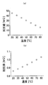
- FIG. 7A shows the relationship between the temperature and the resistance value of the first channel 21 in the first embodiment.
- FIG. 7B shows the relationship between the temperature and the resistance value of the second channel 23.
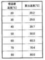
- FIG. 8 shows a table comparing the temperature of the thermostatic chamber and the temperature calculated from the output voltage in Example 1.
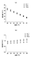
- FIG. 9 shows a graph in which the horizontal axis represents the channel size ratio ⁇ and the vertical axis represents the output change in the second embodiment.
- FIG. 10A shows the relationship between the temperature in Example 3 and the resistance value of the first channel 21 when different materials are used in the ferroelectric layer 7.
- FIG. 10B shows the relationship between the temperature in Example 3 and the resistance value of the second channel 23 when different materials are used in the ferroelectric layer 7.
- FIG. 11 shows a table comparing the temperature of the thermostatic chamber and the calculated temperature from the output voltage in Example 3.
- FIG. 12 shows the relationship between the thickness of the ferroelectric layer 7 and the output voltage of the pyroelectric temperature sensor when the temperature rises from 20 ° C. to 80 ° C. in Example 4.
- FIG. 13 shows the relationship between the thickness of the semiconductor layer 9 and the output voltage of the pyroelectric temperature sensor when the temperature rises from 20 ° C. to 80 ° C. in Example 5.
- FIG. 14 is a cross-sectional view of the pyroelectric temperature sensor disclosed in Patent Document 1.
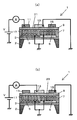
- FIG. 15 shows the pyroelectric temperature sensor 1 and the arithmetic unit of the present invention.
- FIG. 1 shows a pyroelectric temperature sensor according to the first embodiment.
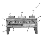
- the pyroelectric temperature sensor 1 includes a substrate 2, a support film 3, lower electrode groups 5 and 6, a ferroelectric layer 7, a semiconductor layer 9, and upper electrode groups 11, 13, and 15. It has.
- the lower electrode groups 5 and 6, the ferroelectric layer 7, the semiconductor layer 9, and the upper electrode groups 11, 13, and 15 are laminated in this order.
- the lower electrode group includes a first lower electrode 5 and a second lower electrode 6.
- the upper electrode group includes a first upper electrode 11, a second upper electrode 13, and a third upper electrode 15.
- the second upper electrode 13 is sandwiched between the first upper electrode 11 and the third upper electrode 15.
- the first ferroelectric portion 7 a of the ferroelectric layer 7 is sandwiched between the first lower electrode 5 and the first upper electrode 11.
- the second ferroelectric portion 7 b of the ferroelectric layer 7 is sandwiched between the second lower electrode 6 and the third upper electrode 15.
- the second ferroelectric portion 7b has a polarization direction opposite to the polarization direction of the first ferroelectric portion 7a.
- the first channel 21 is formed in the portion of the semiconductor layer 9 sandwiched between the first upper electrode 11 and the second upper electrode 13.
- the first ferroelectric portion 7 a is located below the first channel 21.
- the second channel 23 is formed in the portion of the semiconductor layer 9 sandwiched between the second upper electrode 13 and the third upper electrode 15.
- the second ferroelectric portion 7 b is located below the second channel 23.
- 1, 3, 4, and 5 indicate the direction of polarization 17.
- a positive charge is biased at the tip of the arrow.
- the polarization 17 is defined to be upward when the tip of the arrow faces the semiconductor layer 9.
- the polarization 17 is defined as downward.
- the output voltage V out represents the potential of the second upper electrode 13 measured by the voltmeter 81.
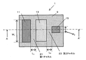
- FIG. 2 is a top view of the pyroelectric temperature sensor according to the first embodiment.
- FIG. 1 is a cross-sectional view taken along line A-A ′ of FIG.
- the first upper electrode 11 and the second upper electrode 13 function as a drain electrode and a source electrode of the first channel 21, respectively.
- the second upper electrode 13 and the third upper electrode 15 function as a drain electrode and a source electrode of the second channel 23, respectively.
- the first channel 21 has a width of W 1 and a length of L 1 .
- the second channel 23 has a width of W 2 and a length of L 2 .
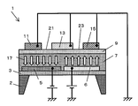
- FIG. 3 shows a cross-sectional view of the pyroelectric temperature sensor in the initial state. As shown in FIG. 3, in the initial state, the direction of polarization 17 is often not determined.
- FIG. 4 shows a method for determining the direction of the polarization 17.
- a negative voltage and a positive voltage are applied to the first lower electrode 5 and the second lower electrode 6 while the first upper electrode 11, the second upper electrode 13, and the third upper electrode 15 are grounded. Is applied. Thereafter, the voltage is removed.
- the polarization 17 is determined as shown in FIG. That is, the direction of the polarization 17 in the first ferroelectric portion 7a of the ferroelectric layer 7 located below the first channel 21 is determined so as to be downward.
- the direction of the polarization 17 in the second ferroelectric portion 7b of the ferroelectric layer 7 located below the second channel 23 is determined to be upward.
- FIGS. 5A and 5B show a method of measuring the resistance values of the first channel 21 and the second channel 23, respectively.
- a positive voltage is applied to the first upper electrode 11 while the second upper electrode 13, the first lower electrode 5, and the second lower electrode 6 are grounded, and the first channel The value of the current flowing through 21 is measured. Furthermore, the relationship between the resistance value of the first channel 21 and the temperature is obtained by changing the temperature of the pyroelectric temperature sensor 1 using a heating means (not shown).
- a positive voltage is applied to the second upper electrode 13 while the third upper electrode 15, the first lower electrode 5, and the second lower electrode 6 are grounded, and the second channel The value of the current flowing through 23 is measured.
- the relationship between the resistance value of the second channel 23 and the temperature is obtained by changing the temperature of the pyroelectric temperature sensor 1 using a heating means (not shown).
- resistance values R d1 , R u1 , R d2 and R u2 are obtained.
- R d1 represents the resistance value of the first channel 21 when the temperature T of the ferroelectric layer 7 is T 1 .
- R u1 represents the resistance value of the second channel 23 when the temperature T of the ferroelectric layer 7 is T 1 .
- R d2 represents the resistance value of the first channel 21 when the temperature T of the ferroelectric layer 7 is T 2 .
- R u2 represents the resistance value of the second channel 23 when the temperature T of the ferroelectric layer 7 is T 2 .
- the power supply voltage V DD is applied to the first upper electrode 11.
- the power supply voltage V DD is distributed according to the resistance value R u of the resistance R d and the second channel 23 of the first channel 21, and the potential of the second upper electrode 13 is output as the output voltage V out.
- the present inventors obtain the temperature T of the ferroelectric layer 7. It was found that ° C can be measured.
- the present inventors have found that the resistance value of a channel is proportional to the temperature of the channel. Furthermore, the present inventors have also found a relationship that when the polarization direction in the ferroelectric layer 7 is reversed, the proportional gradient is also reversed.
- the resistance value of the first channel 21 decreases.
- the decrease in the resistance value of the first channel 21 is proportional to the increase in the temperature.
- the resistance value of the second channel 23 increases.
- the increase in the resistance value of the second channel 23 is proportional to the increase in the temperature.
- the resistance value of the first channel 21 increases.
- the increase in the resistance value of the first channel 21 is proportional to the decrease in the temperature.
- the resistance value of the second channel 23 decreases.
- the decrease in the resistance value of the second channel 23 is proportional to the decrease in the temperature.
- the pyroelectric temperature sensor of the present invention can be used for temperature measurement at 150 ° C. or lower. When the temperature exceeds 150 ° C., polarization can become unstable.
- the pyroelectric temperature sensor of the present invention is preferably used for temperature measurement of ⁇ 20 ° C. or higher.
- the pyroelectric temperature sensor of the present invention has higher sensitivity to temperature than the conventional pyroelectric temperature sensor.
- the temperature measuring device of the present invention includes the pyroelectric temperature sensor and the arithmetic device described above.
- the arithmetic device includes a processing unit, a storage unit, an output unit, and an input unit.
- the output voltage V OUT from the second upper electrode 13 is input to the input unit.
- the storage unit stores a constant Rd 1 , a constant Ru 1 , a constant Rd 2 , and a constant Ru 2 . These constants are stored in the storage unit until the temperature measuring device mass-produced in the factory is shipped from the factory. That is, a temperature measuring device in which these constants are stored at the time of factory shipment is included in the spirit of the present invention.
- the user of the temperature measuring device of the present invention causes the temperature sensor to touch an object for which the user wants to know the temperature.
- the processing unit calculates the temperature T based on the above equation (2) while referring to the storage unit. Then, the output unit outputs the calculated temperature T. In this way, the user knows the temperature T of the object.
- the object can be a gas, a liquid, or a solid.
- FIG. 6 shows a method for manufacturing a pyroelectric temperature sensor.
- A An SrTiO 3 thin film having a thickness of 150 nm is deposited on the MgO (100) single crystal substrate 2 at a temperature of 700 ° C. by a pulsed laser deposition method (hereinafter referred to as “PLD method”). Film 3 was formed.
- PLD method pulsed laser deposition method
- a platinum film having a thickness of 200 nm was deposited by the PLD method.
- a resist (not shown) was applied and patterned to form an etching mask.
- the platinum film was etched by a reactive ion etching method using CF 4 gas. Thereafter, the resist was removed, and the first lower electrode 5 and the second lower electrode 6 were formed as shown in FIG.
- a resist (not shown) was applied and patterned. Further, a platinum film having a thickness of 50 nm was deposited using EB vapor deposition. As shown in FIG. 6C, the first upper electrode 11, the second upper electrode 13, and the third upper electrode 15 were formed by using a lift-off method for removing the resist.
- Example 1 the width W 1 and length L 1 of the first channel 21 and the width W 2 and length L 2 of the second channel 23 were 1000 ⁇ m, 1 ⁇ m, 10 ⁇ m, and 10 ⁇ m, respectively.
- the channel size ratio ⁇ was 1000.
- the pyroelectric temperature sensor was placed in a constant temperature bath (not shown) at 20 ° C., and the resistance value R d1 of the first channel 21 and the resistance value R u1 of the second channel 23 were measured.
- R d1 was 45 megohm and R u1 was 0.86 megohm.
- the temperature of the constant temperature bath was changed to 30 ° C., 40 ° C., 50 ° C., 60 ° C., and 70 ° C., and the resistance value of the first channel 21 and the resistance value of the second channel 23 were measured.
- the temperature of the thermostatic chamber was changed to 80 ° C., and the resistance value R d2 of the first channel 21 and the resistance value R u2 of the second channel 23 were measured.
- R d2 was 16 megohms and R u2 was 1.0 megohms.
- FIG. 7A shows the relationship between the temperature and the resistance value of the first channel 21 obtained by the above measurement.
- FIG. 7B shows the relationship between the temperature and the resistance value of the second channel 23.
- the power supply voltage V DD was 100 mV.
- FIG. 8 shows a table comparing the temperature of the thermostat and the temperature calculated from the output voltage based on equation (2). As shown in FIG. 8, the actual temperature coincided with the calculated temperature.
- FIG. 9 is a graph in which the horizontal axis represents the channel size ratio ⁇ and the vertical axis represents the change in output voltage.
- the change in output voltage means a change in the output voltage of the pyroelectric temperature sensor when the temperature rises from 20 ° C. to 80 ° C. As shown in FIG. 9, the output change increases as ⁇ increases. Since the detection lower limit of the voltage change is 0.1 mV, a detectable output voltage change can be obtained when ⁇ is 30 or more. Since an output voltage change of 1 mV or more is obtained, ⁇ is preferably 300 or more.
- FIG. 10A shows the relationship between the temperature and the resistance value of the first channel 21 when different materials are used in the ferroelectric layer 7.
- FIG. 10B shows the relationship between the temperature and the resistance value of the second channel 23 when different materials are used in the ferroelectric layer 7.
- the first channel 21 and the second channel 23 have the same size as those in the first embodiment.
- Example 3 Pb (Zr, Ti) O 3 (PZT) and PbTiO 3 (PTO) having a Zr: Ti ratio of 0.4: 0.6 were used instead of PLT.
- R d1 , R u1 , R d2 , and R u2 were 43 megaohms, 0.75 megaohms, 14 megaohms, and 0.87 megaohms, respectively.
- R d1 , R u1 , R d2 , and R u2 were 48 megaohms, 0.94 megaohms, 16 megaohms, and 1.1 megaohms, respectively.
- R d1 and R u1 were obtained when the temperature of the thermostatic bath was 20 ° C.
- R d2 and R u2 were obtained when the temperature of the thermostatic bath was 80 ° C.
- FIG. 11 shows a table comparing the temperature of the thermostat and the temperature calculated from the output voltage based on equation (2). As shown in FIG. 11, the actual temperature coincided with the calculated temperature.
- Example 4 the output voltage of the pyroelectric temperature sensor when the thickness of the ferroelectric layer 7 was changed was measured.
- FIG. 12 shows the relationship between the thickness of the ferroelectric layer 7 and the change in output voltage of the pyroelectric temperature sensor when the temperature rises from 20 ° C. to 80 ° C.
- the change in output voltage is reduced.
- the output voltage change is preferably 1 mV or more.
- the ferroelectric layer 7 in order to obtain a change in output voltage of 1 mV or more, the ferroelectric layer 7 preferably has a thickness of 40 nm or more.
- Example 5 In Example 5, the output voltage of the pyroelectric temperature sensor when the thickness of the semiconductor layer 9 was changed was measured.
- FIG. 13 shows the relationship between the thickness of the semiconductor layer 9 and the change in output voltage of the pyroelectric temperature sensor when the temperature rises from 20 ° C. to 80 ° C.
- the output voltage decreased as the thickness of the semiconductor layer 9 increased.
- the change in output voltage becomes less than the detection lower limit (0.1 mV). Therefore, as understood from FIG. 13, the semiconductor layer 9 preferably has a thickness of 70 nm or less.
- the temperature of various objects can be measured by the method of the present invention.
Abstract
A series transistor structure is formed by a semiconductor layer (9) and three upper electrodes (11, 13, 15). The semiconductor layer (9) is of a structure which is in contact with a ferroelectric layer (7), and when the direction of polarization is vertically changed with respect to the two transistors, the polarities of the temperature characteristics of two channels can be inverted to each other.
Description
本発明は、焦電型温度センサを用いて温度を測定する方法に関する。
The present invention relates to a method for measuring temperature using a pyroelectric temperature sensor.
温度変化により焦電体表面の電荷量が増減する。これは、焦電効果と呼ばれる。焦電型温度センサは、焦電効果を利用して温度を検出する。特許文献1は、焦電体/半導体構造を備える従来の焦電型温度センサを開示している。
¡The amount of charge on the pyroelectric surface increases or decreases due to temperature changes. This is called the pyroelectric effect. The pyroelectric temperature sensor detects temperature using the pyroelectric effect. Patent Document 1 discloses a conventional pyroelectric temperature sensor having a pyroelectric body / semiconductor structure.
図14は、特許文献1に開示された焦電型温度センサの断面図を示す。当該焦電型温度センサは、焦電薄膜101、センサ電極102、半導体薄膜103、ソース電極104、ドレイン電極105、層間絶縁膜106、および引き出し電極107を具備する。
FIG. 14 is a cross-sectional view of the pyroelectric temperature sensor disclosed in Patent Document 1. The pyroelectric temperature sensor includes a pyroelectric thin film 101, a sensor electrode 102, a semiconductor thin film 103, a source electrode 104, a drain electrode 105, an interlayer insulating film 106, and a lead electrode 107.
温度の変化を原因とする焦電効果により、焦電薄膜101と半導体層103との界面の近傍の部分の電位が変調される。この変調が、チャネル領域または空乏層を形成する。当該形成は導電率を大きく変化する。このようにして、焦電薄膜における温度の変化が薄膜トランジスタのドレイン電流の変化に変換される。
The potential in the vicinity of the interface between the pyroelectric thin film 101 and the semiconductor layer 103 is modulated by the pyroelectric effect caused by the temperature change. This modulation forms a channel region or depletion layer. This formation greatly changes the conductivity. In this way, a change in temperature in the pyroelectric thin film is converted into a change in the drain current of the thin film transistor.
しかし、特許文献1によれば、薄膜トランジスタの増幅特性を超える効果が得られない。さらに、ドレイン電流量の検出は、複雑な外部回路を必要とする。
However, according to Patent Document 1, an effect exceeding the amplification characteristics of the thin film transistor cannot be obtained. Furthermore, the detection of the drain current amount requires a complicated external circuit.
本発明の目的は、より高い感度を有する小型の焦電型温度センサを用いて温度を測定する方法を提供することである。
An object of the present invention is to provide a method for measuring temperature using a small pyroelectric temperature sensor having higher sensitivity.
本発明は、温度センサを用いて温度を測定する方法を提供する。当該方法は、以下の工程を具備する:
前記温度センサを準備する工程、
ここで、前記温度センサは、下部電極群、強誘電体層、半導体層、および上部電極群を具備しており、
前記下部電極群、前記強誘電体層、前記半導体層、および前記上部電極群は、この順で積層されており、
前記下部電極群は、第1の下部電極および第2の下部電極を具備しており、
前記上部電極群は、第1の上部電極、第2の上部電極、および第3の上部電極を具備しており、
前記第2の上部電極は、前記第1の上部電極と前記第3の上部電極との間に挟まれており、
前記第1の下部電極と前記第1の上部電極との間に、前記強誘電体層の第1強誘電体部分が挟まれ、
前記第2の下部電極と前記第3の上部電極との間に、前記強誘電体層の第2強誘電体部分が挟まれ、
前記第1強誘電体部分の分極方向は、前記第2強誘電体部分の分極方向とは逆であり、
前記第1の上部電極と前記第2の上部電極との間に挟まれる前記半導体層の部分に第1チャネルが形成されており、
前記第2の上部電極と前記第3の上部電極との間に挟まれる前記半導体層の部分に第2チャネルが形成されており、
前記第1の上部電極および前記第3の上部電極に、それぞれ電圧VDDおよび0Vを印加し、第2の上部電極からの出力電圧VOUTを測定する工程、
以下の等式(2)から温度Tを算出する工程

ここで、Rd1は、強誘電体層の温度TがT1の時の前記第1チャネルの抵抗値を表し、
Ru1は、強誘電体層の温度TがT1の時の第2チャネルの抵抗値を表し、
Rd2は、強誘電体層の温度TがT2の時の第1チャネルの抵抗値を表し、そして
Ru2は、強誘電体層の温度TがT2の時の第2チャネルの抵抗値を表す。 The present invention provides a method for measuring temperature using a temperature sensor. The method comprises the following steps:
Preparing the temperature sensor;
Here, the temperature sensor includes a lower electrode group, a ferroelectric layer, a semiconductor layer, and an upper electrode group,
The lower electrode group, the ferroelectric layer, the semiconductor layer, and the upper electrode group are laminated in this order,
The lower electrode group includes a first lower electrode and a second lower electrode,
The upper electrode group includes a first upper electrode, a second upper electrode, and a third upper electrode,
The second upper electrode is sandwiched between the first upper electrode and the third upper electrode;
A first ferroelectric portion of the ferroelectric layer is sandwiched between the first lower electrode and the first upper electrode;
A second ferroelectric portion of the ferroelectric layer is sandwiched between the second lower electrode and the third upper electrode;
The polarization direction of the first ferroelectric portion is opposite to the polarization direction of the second ferroelectric portion;
A first channel is formed in a portion of the semiconductor layer sandwiched between the first upper electrode and the second upper electrode;
A second channel is formed in a portion of the semiconductor layer sandwiched between the second upper electrode and the third upper electrode;
Applying voltages V DD and 0 V to the first upper electrode and the third upper electrode, respectively, and measuring an output voltage V OUT from the second upper electrode;
Step of calculating temperature T from equation (2) below
Here, R d1 represents the resistance value of the first channel when the temperature T of the ferroelectric layer is T 1 ,
R u1 represents the resistance value of the second channel when the temperature T of the ferroelectric layer is T 1 ,
R d2 represents the resistance value of the first channel when the temperature T of the ferroelectric layer is T 2 , and R u2 represents the resistance value of the second channel when the temperature T of the ferroelectric layer is T 2. Represents.
前記温度センサを準備する工程、
ここで、前記温度センサは、下部電極群、強誘電体層、半導体層、および上部電極群を具備しており、
前記下部電極群、前記強誘電体層、前記半導体層、および前記上部電極群は、この順で積層されており、
前記下部電極群は、第1の下部電極および第2の下部電極を具備しており、
前記上部電極群は、第1の上部電極、第2の上部電極、および第3の上部電極を具備しており、
前記第2の上部電極は、前記第1の上部電極と前記第3の上部電極との間に挟まれており、
前記第1の下部電極と前記第1の上部電極との間に、前記強誘電体層の第1強誘電体部分が挟まれ、
前記第2の下部電極と前記第3の上部電極との間に、前記強誘電体層の第2強誘電体部分が挟まれ、
前記第1強誘電体部分の分極方向は、前記第2強誘電体部分の分極方向とは逆であり、
前記第1の上部電極と前記第2の上部電極との間に挟まれる前記半導体層の部分に第1チャネルが形成されており、
前記第2の上部電極と前記第3の上部電極との間に挟まれる前記半導体層の部分に第2チャネルが形成されており、
前記第1の上部電極および前記第3の上部電極に、それぞれ電圧VDDおよび0Vを印加し、第2の上部電極からの出力電圧VOUTを測定する工程、
以下の等式(2)から温度Tを算出する工程
Ru1は、強誘電体層の温度TがT1の時の第2チャネルの抵抗値を表し、
Rd2は、強誘電体層の温度TがT2の時の第1チャネルの抵抗値を表し、そして
Ru2は、強誘電体層の温度TがT2の時の第2チャネルの抵抗値を表す。 The present invention provides a method for measuring temperature using a temperature sensor. The method comprises the following steps:
Preparing the temperature sensor;
Here, the temperature sensor includes a lower electrode group, a ferroelectric layer, a semiconductor layer, and an upper electrode group,
The lower electrode group, the ferroelectric layer, the semiconductor layer, and the upper electrode group are laminated in this order,
The lower electrode group includes a first lower electrode and a second lower electrode,
The upper electrode group includes a first upper electrode, a second upper electrode, and a third upper electrode,
The second upper electrode is sandwiched between the first upper electrode and the third upper electrode;
A first ferroelectric portion of the ferroelectric layer is sandwiched between the first lower electrode and the first upper electrode;
A second ferroelectric portion of the ferroelectric layer is sandwiched between the second lower electrode and the third upper electrode;
The polarization direction of the first ferroelectric portion is opposite to the polarization direction of the second ferroelectric portion;
A first channel is formed in a portion of the semiconductor layer sandwiched between the first upper electrode and the second upper electrode;
A second channel is formed in a portion of the semiconductor layer sandwiched between the second upper electrode and the third upper electrode;
Applying voltages V DD and 0 V to the first upper electrode and the third upper electrode, respectively, and measuring an output voltage V OUT from the second upper electrode;
Step of calculating temperature T from equation (2) below
R u1 represents the resistance value of the second channel when the temperature T of the ferroelectric layer is T 1 ,
R d2 represents the resistance value of the first channel when the temperature T of the ferroelectric layer is T 2 , and R u2 represents the resistance value of the second channel when the temperature T of the ferroelectric layer is T 2. Represents.
上記の温度センサもまた、本発明の趣旨に包含される。
The above temperature sensor is also included in the spirit of the present invention.
上記の温度センサおよび演算装置を備えた温度測定装置も本発明の趣旨に包含される。
A temperature measuring device provided with the above temperature sensor and arithmetic device is also included in the spirit of the present invention.
ここで、前記演算装置は、処理部、記憶部、出力部、および入力部を具備し、
前記入力部には前記第2の上部電極からの出力電圧VOUTが入力され、
前記記憶部は、定数Rd1、定数Ru1、定数Rd2、および定数Ru2を記憶しており、
前記処理部は、前記記憶部を参照しながら上記の等式(2)に基づいて温度Tを算出し、
前記出力部は、算出された前記温度Tを出力する。 Here, the arithmetic device includes a processing unit, a storage unit, an output unit, and an input unit,
An output voltage V OUT from the second upper electrode is input to the input unit,
The storage unit stores a constant Rd1, a constant Ru1, a constant Rd2, and a constant Ru2.
The processing unit calculates the temperature T based on the above equation (2) while referring to the storage unit,
The output unit outputs the calculated temperature T.
本発明は高感度な焦電型温度センサを用いて温度を測定する方法を提供する。
The present invention provides a method for measuring temperature using a highly sensitive pyroelectric temperature sensor.
図面を参照しながら、本発明の実施の形態が以下、説明される。
Embodiments of the present invention will be described below with reference to the drawings.
(実施の形態1)
図1は、実施の形態1による焦電型温度センサを示す。 (Embodiment 1)
FIG. 1 shows a pyroelectric temperature sensor according to the first embodiment.
図1は、実施の形態1による焦電型温度センサを示す。 (Embodiment 1)
FIG. 1 shows a pyroelectric temperature sensor according to the first embodiment.
図1に示されるように、本焦電型温度センサ1は、基板2、支持膜3、下部電極群5・6、強誘電体層7、半導体層9、上部電極群11・13・15を具備する。
As shown in FIG. 1, the pyroelectric temperature sensor 1 includes a substrate 2, a support film 3, lower electrode groups 5 and 6, a ferroelectric layer 7, a semiconductor layer 9, and upper electrode groups 11, 13, and 15. It has.
下部電極群5・6、強誘電体層7、半導体層9、および上部電極群11・13・15は、この順で積層されている。
The lower electrode groups 5 and 6, the ferroelectric layer 7, the semiconductor layer 9, and the upper electrode groups 11, 13, and 15 are laminated in this order.
下部電極群は、第1の下部電極5および第2の下部電極6を具備している。
The lower electrode group includes a first lower electrode 5 and a second lower electrode 6.
上部電極群は、第1の上部電極11、第2の上部電極13、および第3の上部電極15を具備している。
The upper electrode group includes a first upper electrode 11, a second upper electrode 13, and a third upper electrode 15.
第2の上部電極13は、第1の上部電極11と第3の上部電極15との間に挟まれている。
The second upper electrode 13 is sandwiched between the first upper electrode 11 and the third upper electrode 15.
第1の下部電極5と第1の上部電極11との間に、強誘電体層7の第1強誘電体部分7aが挟まれている。
The first ferroelectric portion 7 a of the ferroelectric layer 7 is sandwiched between the first lower electrode 5 and the first upper electrode 11.
第2の下部電極6と第3の上部電極15との間に、強誘電体層7の第2強誘電体部分7bが挟まれている。
The second ferroelectric portion 7 b of the ferroelectric layer 7 is sandwiched between the second lower electrode 6 and the third upper electrode 15.
第2強誘電体部分7bは、第1強誘電体部分7aの分極方向とは逆の分極方向を有している。
The second ferroelectric portion 7b has a polarization direction opposite to the polarization direction of the first ferroelectric portion 7a.
第1の上部電極11と第2の上部電極13との間に挟まれる半導体層9の部分に第1チャネル21が形成されている。第1強誘電体部分7aは、第1チャネル21の下に位置している。
The first channel 21 is formed in the portion of the semiconductor layer 9 sandwiched between the first upper electrode 11 and the second upper electrode 13. The first ferroelectric portion 7 a is located below the first channel 21.
第2の上部電極13と第3の上部電極15との間に挟まれる半導体層9の部分に第2チャネル23が形成されている。第2強誘電体部分7bは、第2チャネル23の下に位置している。
The second channel 23 is formed in the portion of the semiconductor layer 9 sandwiched between the second upper electrode 13 and the third upper electrode 15. The second ferroelectric portion 7 b is located below the second channel 23.
図1、図3、図4、および図5における矢印は、分極17の方向を表す。本明細書では、当該矢印の先端に正の電荷が偏っていることが定義される。本明細書では、矢印の先端が半導体層9に向いている場合には、分極17は上向きであると定義される。一方、矢印の先端が支持膜3を向いている場合には、分極17は下向きであると定義される。
1, 3, 4, and 5 indicate the direction of polarization 17. In the present specification, it is defined that a positive charge is biased at the tip of the arrow. In the present specification, the polarization 17 is defined to be upward when the tip of the arrow faces the semiconductor layer 9. On the other hand, when the tip of the arrow faces the support film 3, the polarization 17 is defined as downward.
図1において、出力電圧Voutは、電圧計81によって測定される第2上部電極13の電位を表す。
In FIG. 1, the output voltage V out represents the potential of the second upper electrode 13 measured by the voltmeter 81.
図2は、実施の形態1による焦電型温度センサの上面図を示す。図1は、図2のA-A’断面図である。第1上部電極11および第2上部電極13は、それぞれ、第1チャネル21のドレイン電極およびソース電極として機能する。第2上部電極13および第3上部電極15は、それぞれ、第2チャネル23のドレイン電極およびソース電極として機能する。
FIG. 2 is a top view of the pyroelectric temperature sensor according to the first embodiment. FIG. 1 is a cross-sectional view taken along line A-A ′ of FIG. The first upper electrode 11 and the second upper electrode 13 function as a drain electrode and a source electrode of the first channel 21, respectively. The second upper electrode 13 and the third upper electrode 15 function as a drain electrode and a source electrode of the second channel 23, respectively.
第1チャネル21は、W1の幅およびL1の長さを有する。第2チャネル23は、W2の幅およびL2の長さを有する。
The first channel 21 has a width of W 1 and a length of L 1 . The second channel 23 has a width of W 2 and a length of L 2 .
チャネルサイズ比αは以下の等式(1)により定義される。
α=(W1/L1)/(W2/L2) ・・・(1) The channel size ratio α is defined by the following equation (1).
α = (W 1 / L 1 ) / (W 2 / L 2 ) (1)
α=(W1/L1)/(W2/L2) ・・・(1) The channel size ratio α is defined by the following equation (1).
α = (W 1 / L 1 ) / (W 2 / L 2 ) (1)
図3は、焦電型温度センサの初期状態における断面図を示す。図3に示されるように、初期状態においては、分極17の方向は、しばしば、決められていない。
FIG. 3 shows a cross-sectional view of the pyroelectric temperature sensor in the initial state. As shown in FIG. 3, in the initial state, the direction of polarization 17 is often not determined.
図4は、分極17の方向を決める方法を示す。図4に示されるように、第1上部電極11、第2上部電極13、および第3上部電極15を接地しながら、第1下部電極5および第2下部電極6に、それぞれ負の電圧および正の電圧が印加される。その後、電圧を除去する。このようにして、分極17は図4に示されるように決定される。すなわち、第1チャネル21の下に位置する強誘電体層7の第1強誘電体部分7aにおける分極17の向きは下向きになるように決定される。一方、第2チャネル23の下に位置する強誘電体層7の第2強誘電体部分7bにおける分極17の向きは上向きになるように決定される。
FIG. 4 shows a method for determining the direction of the polarization 17. As shown in FIG. 4, a negative voltage and a positive voltage are applied to the first lower electrode 5 and the second lower electrode 6 while the first upper electrode 11, the second upper electrode 13, and the third upper electrode 15 are grounded. Is applied. Thereafter, the voltage is removed. In this way, the polarization 17 is determined as shown in FIG. That is, the direction of the polarization 17 in the first ferroelectric portion 7a of the ferroelectric layer 7 located below the first channel 21 is determined so as to be downward. On the other hand, the direction of the polarization 17 in the second ferroelectric portion 7b of the ferroelectric layer 7 located below the second channel 23 is determined to be upward.
その後、第1チャネル21および第2チャネル23の抵抗値が測定される。図5(a)および図5(b)は、それぞれ第1チャネル21および第2チャネル23の抵抗値を測定する方法を示す。
Thereafter, the resistance values of the first channel 21 and the second channel 23 are measured. FIGS. 5A and 5B show a method of measuring the resistance values of the first channel 21 and the second channel 23, respectively.
図5(a)に示されるように、第2上部電極13、第1下部電極5、および第2下部電極6が接地されながら、第1上部電極11に正の電圧が印加され、第1チャネル21を流れる電流値を測定する。さらに、加熱手段(図示せず)を用いて焦電型温度センサ1の温度を変化させることによって、第1チャネル21の抵抗値と温度との関係が得られる。
As shown in FIG. 5A, a positive voltage is applied to the first upper electrode 11 while the second upper electrode 13, the first lower electrode 5, and the second lower electrode 6 are grounded, and the first channel The value of the current flowing through 21 is measured. Furthermore, the relationship between the resistance value of the first channel 21 and the temperature is obtained by changing the temperature of the pyroelectric temperature sensor 1 using a heating means (not shown).
図5(b)に示されるように、第3上部電極15、第1下部電極5、および第2下部電極6が接地されながら、第2上部電極13に正の電圧が印加され、第2チャネル23を流れる電流値を測定する。図5(a)と同様に、加熱手段(図示せず)を用いて焦電型温度センサ1の温度を変化させることによって、第2チャネル23の抵抗値と温度との関係が得られる。
As shown in FIG. 5B, a positive voltage is applied to the second upper electrode 13 while the third upper electrode 15, the first lower electrode 5, and the second lower electrode 6 are grounded, and the second channel The value of the current flowing through 23 is measured. Similarly to FIG. 5A, the relationship between the resistance value of the second channel 23 and the temperature is obtained by changing the temperature of the pyroelectric temperature sensor 1 using a heating means (not shown).
このようにして、抵抗値Rd1、Ru1、Rd2、およびRu2が得られる。
Rd1は、強誘電体層7の温度TがT1の時の第1チャネル21の抵抗値を表す。
Ru1は、強誘電体層7の温度TがT1の時の第2チャネル23の抵抗値を表す。
Rd2は、強誘電体層7の温度TがT2の時の第1チャネル21の抵抗値を表す。
Ru2は、強誘電体層7の温度TがT2の時の第2チャネル23の抵抗値を表す。 In this way, resistance values R d1 , R u1 , R d2 and R u2 are obtained.
R d1 represents the resistance value of thefirst channel 21 when the temperature T of the ferroelectric layer 7 is T 1 .
R u1 represents the resistance value of thesecond channel 23 when the temperature T of the ferroelectric layer 7 is T 1 .
R d2 represents the resistance value of thefirst channel 21 when the temperature T of the ferroelectric layer 7 is T 2 .
R u2 represents the resistance value of thesecond channel 23 when the temperature T of the ferroelectric layer 7 is T 2 .
Rd1は、強誘電体層7の温度TがT1の時の第1チャネル21の抵抗値を表す。
Ru1は、強誘電体層7の温度TがT1の時の第2チャネル23の抵抗値を表す。
Rd2は、強誘電体層7の温度TがT2の時の第1チャネル21の抵抗値を表す。
Ru2は、強誘電体層7の温度TがT2の時の第2チャネル23の抵抗値を表す。 In this way, resistance values R d1 , R u1 , R d2 and R u2 are obtained.
R d1 represents the resistance value of the
R u1 represents the resistance value of the
R d2 represents the resistance value of the
R u2 represents the resistance value of the
次に、温度を測定する方法が説明される。
Next, a method for measuring temperature will be described.
図1に示されるように、電源電圧VDDが第1の上部電極11に印加される。当該電源電圧VDDは、第1チャネル21の抵抗値Rdおよび第2チャネル23の抵抗値Ruに従って分配され、そして第2の上部電極13の電位が出力電圧Voutとして出力される。
As shown in FIG. 1, the power supply voltage V DD is applied to the first upper electrode 11. The power supply voltage V DD is distributed according to the resistance value R u of the resistance R d and the second channel 23 of the first channel 21, and the potential of the second upper electrode 13 is output as the output voltage V out.
温度Tの変化に従って抵抗値Rdおよび抵抗値Ruが変化する。これは、出力電圧Voutが変化することをもらたす。
As the temperature T changes, the resistance value R d and the resistance value R u change. This gives the output voltage V out to change.
本発明者らは、出力電圧Vout、抵抗値Rd1、抵抗値Ru1、抵抗値Rd2、および抵抗値Ru2を含む以下の等式(2)から、強誘電体層7の温度T℃を測定できることを見出した。

From the following equation (2) including the output voltage V out , the resistance value R d1 , the resistance value R u1 , the resistance value R d2 , and the resistance value R u2 , the present inventors obtain the temperature T of the ferroelectric layer 7. It was found that ° C can be measured.
図7に示されるように、本発明者らは、チャネルの抵抗値が当該チャネルの温度に比例することを見出した。さらに、本発明者らは、強誘電体層7における分極の向きが反転されると、当該比例の傾きも反転するという関係も見出した。
As shown in FIG. 7, the present inventors have found that the resistance value of a channel is proportional to the temperature of the channel. Furthermore, the present inventors have also found a relationship that when the polarization direction in the ferroelectric layer 7 is reversed, the proportional gradient is also reversed.
すなわち、下向きの分極17を有する第1強誘電体部分7aに接する第1チャネル21の温度が上昇すると、当該第1チャネル21の抵抗値は低下する。当該第1チャネル21の抵抗値の低下は、当該温度の上昇に比例する。
That is, when the temperature of the first channel 21 in contact with the first ferroelectric portion 7a having the downward polarization 17 increases, the resistance value of the first channel 21 decreases. The decrease in the resistance value of the first channel 21 is proportional to the increase in the temperature.
一方、上向きの分極17を有する第2強誘電体部分7bに接する第2チャネル23の温度が上昇すると、当該第2チャネル23の抵抗値は上昇する。当該第2チャネル23の抵抗値の上昇は、当該温度の上昇に比例する。
On the other hand, when the temperature of the second channel 23 in contact with the second ferroelectric portion 7b having the upward polarization 17 increases, the resistance value of the second channel 23 increases. The increase in the resistance value of the second channel 23 is proportional to the increase in the temperature.
言うまでもないが、下向きの分極を有する第1強誘電体部分7aに接する第1チャネル21の温度が低下すると、当該第1チャネル21の抵抗値は上昇する。当該第1チャネル21の抵抗値の上昇は、当該温度の低下に比例する。
Needless to say, when the temperature of the first channel 21 in contact with the first ferroelectric portion 7a having downward polarization decreases, the resistance value of the first channel 21 increases. The increase in the resistance value of the first channel 21 is proportional to the decrease in the temperature.
一方、上向きの分極を有する第2強誘電体部分7bに接する第2チャネル23の温度が低下すると、当該第2チャネルの抵抗値は低下する。当該第2チャネル23の抵抗値の低下は、当該温度の低下に比例する。
On the other hand, when the temperature of the second channel 23 in contact with the second ferroelectric portion 7b having upward polarization decreases, the resistance value of the second channel decreases. The decrease in the resistance value of the second channel 23 is proportional to the decrease in the temperature.
本発明の焦電型温度センサは、150℃以下の温度測定に用いられ得る。温度が150℃を超える場合、分極が不安定になり得る。本発明の焦電型温度センサは、-20℃以上の温度測定に用いられることが好ましい。
The pyroelectric temperature sensor of the present invention can be used for temperature measurement at 150 ° C. or lower. When the temperature exceeds 150 ° C., polarization can become unstable. The pyroelectric temperature sensor of the present invention is preferably used for temperature measurement of −20 ° C. or higher.
当該関係のため、従来の焦電型温度センサと比較して、本発明の焦電型温度センサは、温度に対するより高い感度を有する。
Because of this relationship, the pyroelectric temperature sensor of the present invention has higher sensitivity to temperature than the conventional pyroelectric temperature sensor.
本発明の温度測定装置は、上記の焦電型温度センサおよび演算装置を備える。図15に示されるように、演算装置は、処理部、記憶部、出力部、および入力部を具備する。第2の上部電極13からの出力電圧VOUTが入力部に入力される。記憶部は、定数Rd1、定数Ru1、定数Rd2、定数Ru2を記憶している。これらの定数は、工場において量産された当該温度測定装置が当該工場から出荷されるまでに、記憶部に記憶される。すなわち、工場出荷時においてこれらの定数が記憶された温度測定装置は、本発明の趣旨に包含される。
The temperature measuring device of the present invention includes the pyroelectric temperature sensor and the arithmetic device described above. As illustrated in FIG. 15, the arithmetic device includes a processing unit, a storage unit, an output unit, and an input unit. The output voltage V OUT from the second upper electrode 13 is input to the input unit. The storage unit stores a constant Rd 1 , a constant Ru 1 , a constant Rd 2 , and a constant Ru 2 . These constants are stored in the storage unit until the temperature measuring device mass-produced in the factory is shipped from the factory. That is, a temperature measuring device in which these constants are stored at the time of factory shipment is included in the spirit of the present invention.
本発明の温度測定装置のユーザは、そのユーザがその温度を知りたい物体に温度センサを触れさせる。処理部は、記憶部を参照しながら上記の等式(2)に基づいて温度Tを算出する。そして、出力部は、算出された温度Tを出力する。このようにして、当該ユーザは当該物体の温度Tを知る。当該物体は、気体、液体、または固体であり得る。
The user of the temperature measuring device of the present invention causes the temperature sensor to touch an object for which the user wants to know the temperature. The processing unit calculates the temperature T based on the above equation (2) while referring to the storage unit. Then, the output unit outputs the calculated temperature T. In this way, the user knows the temperature T of the object. The object can be a gas, a liquid, or a solid.
(実施例)
以下の実施例は本発明をより詳細に説明する。 (Example)
The following examples illustrate the invention in more detail.
以下の実施例は本発明をより詳細に説明する。 (Example)
The following examples illustrate the invention in more detail.
(実施例1)
図6は、焦電型温度センサを製造する方法を示す。 Example 1
FIG. 6 shows a method for manufacturing a pyroelectric temperature sensor.
図6は、焦電型温度センサを製造する方法を示す。 Example 1
FIG. 6 shows a method for manufacturing a pyroelectric temperature sensor.
(a) 700℃の温度下にて、MgO(100)単結晶基板2の上に、パルスレーザ堆積法(以下、「PLD法」)により、150nmの厚みを有するSrTiO3薄膜が堆積され、支持膜3を形成した。
(A) An SrTiO 3 thin film having a thickness of 150 nm is deposited on the MgO (100) single crystal substrate 2 at a temperature of 700 ° C. by a pulsed laser deposition method (hereinafter referred to as “PLD method”). Film 3 was formed.
基板2の温度を400℃に設定した後、200nmの厚みを有する白金膜がPLD法で堆積された。レジスト(図示せず)が塗布され、かつパターニングされ、エッチングマスクを形成した。CF4ガスを用いた反応性イオンエッチング法により白金膜がエッチングされた。その後、レジストを除去し、図6(a)に示すように、第1下部電極5および第2下部電極6が形成された。
After setting the temperature of the substrate 2 to 400 ° C., a platinum film having a thickness of 200 nm was deposited by the PLD method. A resist (not shown) was applied and patterned to form an etching mask. The platinum film was etched by a reactive ion etching method using CF 4 gas. Thereafter, the resist was removed, and the first lower electrode 5 and the second lower electrode 6 were formed as shown in FIG.
(b) 基板2の温度を600℃に設定した後、500nmの厚みを有する(Pb,La)TiO3膜(PLT膜)がPLD法により堆積された。このようにして、図6(b)に示すように、強誘電体層7が堆積された。PLT膜のPb:La比は9:1に設定された。基板2の温度を400℃に設定した後、PLD法により、30nmの厚みを有するZnO膜を堆積し、半導体層9を形成した。
(B) After setting the temperature of the substrate 2 to 600 ° C., a (Pb, La) TiO 3 film (PLT film) having a thickness of 500 nm was deposited by the PLD method. In this way, the ferroelectric layer 7 was deposited as shown in FIG. The Pb: La ratio of the PLT film was set to 9: 1. After setting the temperature of the substrate 2 to 400 ° C., a ZnO film having a thickness of 30 nm was deposited by the PLD method to form the semiconductor layer 9.
(c) レジスト(図示せず)が塗布され、かつパターニングされた。さらにEB蒸着を用いて50nmの厚みを有する白金膜を堆積した。レジストを除去するリフトオフ法を用いて、図6(c)に示すように、第1上部電極11、第2上部電極13、および第3上部電極15を形成した。
(C) A resist (not shown) was applied and patterned. Further, a platinum film having a thickness of 50 nm was deposited using EB vapor deposition. As shown in FIG. 6C, the first upper electrode 11, the second upper electrode 13, and the third upper electrode 15 were formed by using a lift-off method for removing the resist.
本実施例1では、第1チャネル21の幅W1および長さL1、ならびに第2チャネル23の幅W2および長さL2は、それぞれ、1000μm、1μm、10μm、および10μmであった。チャネルサイズ比αは1000であった。
In Example 1, the width W 1 and length L 1 of the first channel 21 and the width W 2 and length L 2 of the second channel 23 were 1000 μm, 1 μm, 10 μm, and 10 μm, respectively. The channel size ratio α was 1000.
(d) MgO(100)単結晶基板2の下面にレジスト(図示せず)が塗布され、そしてパターニングされた。その後、80℃に加熱した燐酸を用いて、MgO(100)単結晶基板2の中央部分が溶解された。レジストに保護されない部分のMgOは燐酸によって溶解された。支持膜3は溶解されなかった。図6(d)に示される構造は熱容量を大幅に低減するため、強誘電体層7の温度変化がより敏感に出力電圧VOUTに反映され得る。その後、レジストが除去され、焦電型温度センサを得た。
(D) A resist (not shown) was applied to the lower surface of the MgO (100) single crystal substrate 2 and patterned. Thereafter, the central portion of the MgO (100) single crystal substrate 2 was dissolved using phosphoric acid heated to 80 ° C. The portion of MgO not protected by the resist was dissolved by phosphoric acid. The support membrane 3 was not dissolved. Since the structure shown in FIG. 6D significantly reduces the heat capacity, the temperature change of the ferroelectric layer 7 can be more sensitively reflected in the output voltage VOUT . Thereafter, the resist was removed to obtain a pyroelectric temperature sensor.
当該焦電型温度センサが20℃の恒温槽(図示せず)に配置され、第1チャネル21の抵抗値Rd1および第2チャネル23の抵抗値Ru1を測定した。Rd1は45メガオーム、Ru1は0.86メガオームであった。
The pyroelectric temperature sensor was placed in a constant temperature bath (not shown) at 20 ° C., and the resistance value R d1 of the first channel 21 and the resistance value R u1 of the second channel 23 were measured. R d1 was 45 megohm and R u1 was 0.86 megohm.
次に、恒温槽の温度を30℃、40℃、50℃、60℃、および70℃に変更し、第1チャネル21の抵抗値および第2チャネル23の抵抗値を測定した。
Next, the temperature of the constant temperature bath was changed to 30 ° C., 40 ° C., 50 ° C., 60 ° C., and 70 ° C., and the resistance value of the first channel 21 and the resistance value of the second channel 23 were measured.
最後に、恒温槽の温度を80℃に変更し、第1チャネル21の抵抗値Rd2および第2チャネル23の抵抗値Ru2を測定した。Rd2は16メガオーム、Ru2は1.0メガオームであった。
Finally, the temperature of the thermostatic chamber was changed to 80 ° C., and the resistance value R d2 of the first channel 21 and the resistance value R u2 of the second channel 23 were measured. R d2 was 16 megohms and R u2 was 1.0 megohms.
図7(a)は、上記測定により得られた、温度と第1チャネル21の抵抗値との間の関係を示す。図7(b)は、温度と第2チャネル23の抵抗値との間の関係を示す。電源電圧VDDは100mVであった。
FIG. 7A shows the relationship between the temperature and the resistance value of the first channel 21 obtained by the above measurement. FIG. 7B shows the relationship between the temperature and the resistance value of the second channel 23. The power supply voltage V DD was 100 mV.
図8は、恒温槽の温度と出力電圧から等式(2)に基づいて算出された温度とを比較した表を示す。図8に示されるように、実際の温度は算出された温度に一致した。
FIG. 8 shows a table comparing the temperature of the thermostat and the temperature calculated from the output voltage based on equation (2). As shown in FIG. 8, the actual temperature coincided with the calculated temperature.
(実施例2)
図9は、横軸がチャネルサイズの比αを表し、縦軸が出力電圧変化を表すグラフを示す。当該出力電圧変化は、20℃から80℃へ温度が上昇した際の焦電型温度センサの出力電圧の変化を意味する。図9に示すように、αの上昇に伴い出力変化が大きくなる。電圧変化の検出下限が0.1mVであったので、αが30以上である場合に検出可能な出力電圧変化が得られる。1mV以上の出力電圧変化が得られるため、好ましくは、αは300以上である。 (Example 2)
FIG. 9 is a graph in which the horizontal axis represents the channel size ratio α and the vertical axis represents the change in output voltage. The change in output voltage means a change in the output voltage of the pyroelectric temperature sensor when the temperature rises from 20 ° C. to 80 ° C. As shown in FIG. 9, the output change increases as α increases. Since the detection lower limit of the voltage change is 0.1 mV, a detectable output voltage change can be obtained when α is 30 or more. Since an output voltage change of 1 mV or more is obtained, α is preferably 300 or more.
(実施例3)
図10(a)は、強誘電体層7において異なる材料が用いられた場合における、温度と第1チャネル21の抵抗値との間の関係を示す。図10(b)は、強誘電体層7において異なる材料が用いられた場合における、温度と第2チャネル23の抵抗値との間の関係を示す。第1チャネル21および第2チャネル23は、実施例1のそれらと同じサイズを有する。 (Example 3)
FIG. 10A shows the relationship between the temperature and the resistance value of thefirst channel 21 when different materials are used in the ferroelectric layer 7. FIG. 10B shows the relationship between the temperature and the resistance value of the second channel 23 when different materials are used in the ferroelectric layer 7. The first channel 21 and the second channel 23 have the same size as those in the first embodiment.
図10(a)は、強誘電体層7において異なる材料が用いられた場合における、温度と第1チャネル21の抵抗値との間の関係を示す。図10(b)は、強誘電体層7において異なる材料が用いられた場合における、温度と第2チャネル23の抵抗値との間の関係を示す。第1チャネル21および第2チャネル23は、実施例1のそれらと同じサイズを有する。 (Example 3)
FIG. 10A shows the relationship between the temperature and the resistance value of the
実施例3では、PLTに代えて、0.4:0.6のZr:Ti比を有するPb(Zr,Ti)O3(PZT)およびPbTiO3(PTO)が用いられた。
In Example 3, Pb (Zr, Ti) O 3 (PZT) and PbTiO 3 (PTO) having a Zr: Ti ratio of 0.4: 0.6 were used instead of PLT.
強誘電体層7がPZTからなる場合、Rd1、Ru1、Rd2、およびRu2は、それぞれ、43メガオーム、0.75メガオーム、14メガオーム、および0.87メガオームであった。
When the ferroelectric layer 7 was made of PZT, R d1 , R u1 , R d2 , and R u2 were 43 megaohms, 0.75 megaohms, 14 megaohms, and 0.87 megaohms, respectively.
強誘電体層7がPTOである場合、Rd1、Ru1、Rd2、およびRu2は、それぞれ、48メガオーム、0.94メガオーム、16メガオーム、および1.1メガオームであった。実施例3では、実施例1と同様、恒温槽の温度が20℃の場合にRd1およびRu1は得られた。恒温槽の温度が80℃の場合に、Rd2およびRu2は得られた。
When the ferroelectric layer 7 was PTO, R d1 , R u1 , R d2 , and R u2 were 48 megaohms, 0.94 megaohms, 16 megaohms, and 1.1 megaohms, respectively. In Example 3, as in Example 1, R d1 and R u1 were obtained when the temperature of the thermostatic bath was 20 ° C. R d2 and R u2 were obtained when the temperature of the thermostatic bath was 80 ° C.
図11は、恒温槽の温度と出力電圧から等式(2)に基づいて算出された温度とを比較した表を示す。図11に示されるように、実際の温度は算出された温度に一致した。
FIG. 11 shows a table comparing the temperature of the thermostat and the temperature calculated from the output voltage based on equation (2). As shown in FIG. 11, the actual temperature coincided with the calculated temperature.
(実施例4)
実施例4では、強誘電体層7の厚みを変化させたときの焦電型温度センサの出力電圧を測定した。図12は、強誘電体層7の厚みと、20℃から80℃へ温度が上昇した際の焦電型温度センサの出力電圧変化との関係を示す。 Example 4
In Example 4, the output voltage of the pyroelectric temperature sensor when the thickness of theferroelectric layer 7 was changed was measured. FIG. 12 shows the relationship between the thickness of the ferroelectric layer 7 and the change in output voltage of the pyroelectric temperature sensor when the temperature rises from 20 ° C. to 80 ° C.
実施例4では、強誘電体層7の厚みを変化させたときの焦電型温度センサの出力電圧を測定した。図12は、強誘電体層7の厚みと、20℃から80℃へ温度が上昇した際の焦電型温度センサの出力電圧変化との関係を示す。 Example 4
In Example 4, the output voltage of the pyroelectric temperature sensor when the thickness of the
図12に示されるように、強誘電体層7の厚さが薄くなると、出力電圧変化が小さくなった。特に強誘電体層7の厚さが70nm未満になると出力電圧変化が急速に低下した。安定な検出の観点から、出力電圧変化は1mV以上であることが好ましい。図12から理解されるように、1mV以上の出力電圧変化を得るためには、強誘電体層7は40nm以上の厚みを有することが好ましい。
As shown in FIG. 12, when the thickness of the ferroelectric layer 7 is reduced, the change in output voltage is reduced. In particular, when the thickness of the ferroelectric layer 7 was less than 70 nm, the output voltage change rapidly decreased. From the viewpoint of stable detection, the output voltage change is preferably 1 mV or more. As can be understood from FIG. 12, in order to obtain a change in output voltage of 1 mV or more, the ferroelectric layer 7 preferably has a thickness of 40 nm or more.
(実施例5)
実施例5では、半導体層9の厚みを変化させたときの焦電型温度センサの出力電圧を測定した。図13は、半導体層9の厚みと、20℃から80℃へ温度が上昇した際の焦電型温度センサの出力電圧変化との関係を示す。 (Example 5)
In Example 5, the output voltage of the pyroelectric temperature sensor when the thickness of thesemiconductor layer 9 was changed was measured. FIG. 13 shows the relationship between the thickness of the semiconductor layer 9 and the change in output voltage of the pyroelectric temperature sensor when the temperature rises from 20 ° C. to 80 ° C.
実施例5では、半導体層9の厚みを変化させたときの焦電型温度センサの出力電圧を測定した。図13は、半導体層9の厚みと、20℃から80℃へ温度が上昇した際の焦電型温度センサの出力電圧変化との関係を示す。 (Example 5)
In Example 5, the output voltage of the pyroelectric temperature sensor when the thickness of the
図13に示されるように、半導体層9の厚さが厚くなると、出力電圧が小さくなった。特に半導体層9の厚さが70nmを超えると出力電圧変化が検出下限(0.1mV)以下になる。従って、図13から理解されるように、半導体層9は70nm以下の厚みを有することが好ましい。
As shown in FIG. 13, the output voltage decreased as the thickness of the semiconductor layer 9 increased. In particular, when the thickness of the semiconductor layer 9 exceeds 70 nm, the change in output voltage becomes less than the detection lower limit (0.1 mV). Therefore, as understood from FIG. 13, the semiconductor layer 9 preferably has a thickness of 70 nm or less.
様々な物体の温度が、本発明の方法により測定され得る。
The temperature of various objects can be measured by the method of the present invention.
1 焦電型温度センサ
2 基板
3 支持膜
5 第1下部電極
6 第2下部電極
7 強誘電体層
9 半導体層
11 第1上部電極
13 第2上部電極
15 第3上部電極
17 分極
21 第1チャネル
23 第2チャネル
81 電圧計
W1 第1チャネルの幅
L1 第1チャネルの長さ
W2 第2チャネルの幅
L2 第2チャネルの長さ
Vout 出力電圧(第2上部電極の電位)
VDD 電源電圧
T 強誘電体層の温度
T1 強誘電体層の温度範囲下限
T2 強誘電体層の温度範囲上限
α チャネルサイズ比
Rd 第1チャネルの抵抗値
Rd1 温度T1時の第1チャネルの抵抗値
Rd2 温度T2時の第1チャネルの抵抗値
Ru 第2チャネルの抵抗値
Ru1 温度T1時の第2チャネルの抵抗値
Ru2 温度T2時の第2チャネルの抵抗値 1Pyroelectric Temperature Sensor 2 Substrate 3 Support Film 5 First Lower Electrode 6 Second Lower Electrode 7 Ferroelectric Layer 9 Semiconductor Layer 11 First Upper Electrode 13 Second Upper Electrode 15 Third Upper Electrode 17 Polarization 21 First Channel 23 Second channel 81 Voltmeter W 1 Width of first channel L 1 Length of first channel W 2 Width of second channel L 2 Length of second channel V out output voltage (potential of second upper electrode)
V DD power supply voltage T temperature of ferroelectric layer T 1 temperature range lower limit of ferroelectric layer T 2 temperature range upper limit of ferroelectric layer α channel size ratio R d resistance of first channel R d1 temperature at T 1 the first channel of the resistance R d2 temperature T 2 at the second channel second channel o'clock resistance R u2 temperature T 2 of the resistance value R u times the resistance value R u1 temperature T 1 of the second channel of the first channel Resistance value
2 基板
3 支持膜
5 第1下部電極
6 第2下部電極
7 強誘電体層
9 半導体層
11 第1上部電極
13 第2上部電極
15 第3上部電極
17 分極
21 第1チャネル
23 第2チャネル
81 電圧計
W1 第1チャネルの幅
L1 第1チャネルの長さ
W2 第2チャネルの幅
L2 第2チャネルの長さ
Vout 出力電圧(第2上部電極の電位)
VDD 電源電圧
T 強誘電体層の温度
T1 強誘電体層の温度範囲下限
T2 強誘電体層の温度範囲上限
α チャネルサイズ比
Rd 第1チャネルの抵抗値
Rd1 温度T1時の第1チャネルの抵抗値
Rd2 温度T2時の第1チャネルの抵抗値
Ru 第2チャネルの抵抗値
Ru1 温度T1時の第2チャネルの抵抗値
Ru2 温度T2時の第2チャネルの抵抗値 1
V DD power supply voltage T temperature of ferroelectric layer T 1 temperature range lower limit of ferroelectric layer T 2 temperature range upper limit of ferroelectric layer α channel size ratio R d resistance of first channel R d1 temperature at T 1 the first channel of the resistance R d2 temperature T 2 at the second channel second channel o'clock resistance R u2 temperature T 2 of the resistance value R u times the resistance value R u1 temperature T 1 of the second channel of the first channel Resistance value
Claims (25)
- 温度センサにより温度を測定する方法であって、以下の工程(a)~(c)を具備する:
前記温度センサを準備する工程(a)、
ここで、前記温度センサは、下部電極群、強誘電体層、半導体層、および上部電極群を具備しており、
前記下部電極群、前記強誘電体層、前記半導体層、および前記上部電極群は、この順で積層されており、
前記下部電極群は、第1の下部電極および第2の下部電極を具備しており、
前記上部電極群は、第1の上部電極、第2の上部電極、および第3の上部電極を具備しており、
前記第2の上部電極は、前記第1の上部電極と前記第3の上部電極との間に挟まれており、
前記第1の下部電極と前記第1の上部電極との間に、前記強誘電体層の第1強誘電体部分が挟まれ、
前記第2の下部電極と前記第3の上部電極との間に、前記強誘電体層の第2強誘電体部分が挟まれ、
前記第2強誘電体部分は、前記第1強誘電体部分の分極方向とは逆の分極方向を有し、
前記第1の上部電極と前記第2の上部電極との間に挟まれる前記半導体層の部分に第1チャネルが形成されており、
前記第2の上部電極と前記第3の上部電極との間に挟まれる前記半導体層の部分に第2チャネルが形成されており、
前記第1の上部電極および前記第3の上部電極に、それぞれ電圧VDDおよび0Vを印加し、第2の上部電極からの出力電圧VOUTを測定する工程(b)、
以下の等式(2)から温度Tを算出する工程(c)

Ru1は、強誘電体層の温度TがT1の時の第2チャネルの抵抗値を表し、
Rd2は、強誘電体層の温度TがT2の時の第1チャネルの抵抗値を表し、そして
Ru2は、強誘電体層の温度TがT2の時の第2チャネルの抵抗値を表す。 A method for measuring temperature with a temperature sensor, comprising the following steps (a) to (c):
Preparing the temperature sensor (a),
Here, the temperature sensor includes a lower electrode group, a ferroelectric layer, a semiconductor layer, and an upper electrode group,
The lower electrode group, the ferroelectric layer, the semiconductor layer, and the upper electrode group are laminated in this order,
The lower electrode group includes a first lower electrode and a second lower electrode,
The upper electrode group includes a first upper electrode, a second upper electrode, and a third upper electrode,
The second upper electrode is sandwiched between the first upper electrode and the third upper electrode;
A first ferroelectric portion of the ferroelectric layer is sandwiched between the first lower electrode and the first upper electrode;
A second ferroelectric portion of the ferroelectric layer is sandwiched between the second lower electrode and the third upper electrode;
The second ferroelectric portion has a polarization direction opposite to the polarization direction of the first ferroelectric portion;
A first channel is formed in a portion of the semiconductor layer sandwiched between the first upper electrode and the second upper electrode;
A second channel is formed in a portion of the semiconductor layer sandwiched between the second upper electrode and the third upper electrode;
(B) applying voltages V DD and 0 V to the first upper electrode and the third upper electrode, respectively, and measuring an output voltage V OUT from the second upper electrode;
Step (c) for calculating the temperature T from the following equation (2)
R u1 represents the resistance value of the second channel when the temperature T of the ferroelectric layer is T 1 ,
R d2 represents the resistance value of the first channel when the temperature T of the ferroelectric layer is T 2 , and R u2 represents the resistance value of the second channel when the temperature T of the ferroelectric layer is T 2. Represents. - 前記第1チャネルは、幅W1および長さL1を有しており、
前記第2チャネルは、幅W2および長さL2を有しており、
以下の等式(1)によって表されるチャネルサイズ比αが30以上である、請求項1に記載の方法。
α=(W1/L1)/(W2/L2) ・・・(1) The first channel has a width W 1 and a length L 1 ;
The second channel has a width W 2 and a length L 2 ;
The method according to claim 1, wherein the channel size ratio α represented by the following equation (1) is 30 or more.
α = (W 1 / L 1 ) / (W 2 / L 2 ) (1) - 前記強誘電体層が40nm以上の厚みを有する、請求項1に記載の方法。 The method according to claim 1, wherein the ferroelectric layer has a thickness of 40 nm or more.
- 前記半導体層が70nm以下の厚みを有する、請求項1に記載の方法。 The method according to claim 1, wherein the semiconductor layer has a thickness of 70 nm or less.
- 前記半導体層が70nm以下の厚みを有する、請求項3に記載の方法。 The method according to claim 3, wherein the semiconductor layer has a thickness of 70 nm or less.
- 前記強誘電体層が40nm以上の厚みを有する、請求項2に記載の方法。 The method according to claim 2, wherein the ferroelectric layer has a thickness of 40 nm or more.
- 前記半導体層が70nm以下の厚みを有する、請求項2に記載の方法。 The method according to claim 2, wherein the semiconductor layer has a thickness of 70 nm or less.
- 前記半導体層が70nm以下の厚みを有する、請求項6に記載の方法。 The method according to claim 6, wherein the semiconductor layer has a thickness of 70 nm or less.
- 以下を具備する温度センサ:
前記温度センサは、下部電極群、強誘電体層、半導体層、および上部電極群を具備しており、
前記下部電極群、前記強誘電体層、前記半導体層、および前記上部電極群は、この順で積層されており、
前記下部電極群は、第1の下部電極および第2の下部電極を具備しており、
前記上部電極群は、第1の上部電極、第2の上部電極、および第3の上部電極を具備しており、
前記第2の上部電極は、前記第1の上部電極と前記第3の上部電極との間に挟まれており、
前記第1の下部電極と前記第1の上部電極との間に、前記強誘電体層の第1強誘電体部分が挟まれ、
前記第2の下部電極と前記第3の上部電極との間に、前記強誘電体層の第2強誘電体部分が挟まれ、
前記第2強誘電体部分は、前記第1強誘電体部分の分極方向とは逆の分極方向を有し、
前記第1の上部電極と前記第2の上部電極との間に挟まれる前記半導体層の部分に第1チャネルが形成されており、
前記第2の上部電極と前記第3の上部電極との間に挟まれる前記半導体層の部分に第2チャネルが形成されている。 A temperature sensor comprising:
The temperature sensor includes a lower electrode group, a ferroelectric layer, a semiconductor layer, and an upper electrode group,
The lower electrode group, the ferroelectric layer, the semiconductor layer, and the upper electrode group are laminated in this order,
The lower electrode group includes a first lower electrode and a second lower electrode,
The upper electrode group includes a first upper electrode, a second upper electrode, and a third upper electrode,
The second upper electrode is sandwiched between the first upper electrode and the third upper electrode;
A first ferroelectric portion of the ferroelectric layer is sandwiched between the first lower electrode and the first upper electrode;
A second ferroelectric portion of the ferroelectric layer is sandwiched between the second lower electrode and the third upper electrode;
The second ferroelectric portion has a polarization direction opposite to the polarization direction of the first ferroelectric portion;
A first channel is formed in a portion of the semiconductor layer sandwiched between the first upper electrode and the second upper electrode;
A second channel is formed in a portion of the semiconductor layer sandwiched between the second upper electrode and the third upper electrode. - 前記第1チャネルは、幅W1および長さL1を有しており、
前記第2チャネルは、幅W2および長さL2を有しており、
以下の等式(1)によって表されるチャネルサイズ比αが30以上である、請求項9に記載の温度センサ。
α=(W1/L1)/(W2/L2) ・・・(1) The first channel has a width W 1 and a length L 1 ;
The second channel has a width W 2 and a length L 2 ;
The temperature sensor according to claim 9, wherein the channel size ratio α represented by the following equation (1) is 30 or more.
α = (W 1 / L 1 ) / (W 2 / L 2 ) (1) - 前記強誘電体層が40nm以上の厚みを有する、請求項9に記載の温度センサ。 The temperature sensor according to claim 9, wherein the ferroelectric layer has a thickness of 40 nm or more.
- 前記半導体層が70nm以下の厚みを有する、請求項9に記載の温度センサ。 The temperature sensor according to claim 9, wherein the semiconductor layer has a thickness of 70 nm or less.
- 前記半導体層が70nm以下の厚みを有する、請求項11に記載の温度センサ。 The temperature sensor according to claim 11, wherein the semiconductor layer has a thickness of 70 nm or less.
- 前記強誘電体層が40nm以上の厚みを有する、請求項10に記載の温度センサ。 The temperature sensor according to claim 10, wherein the ferroelectric layer has a thickness of 40 nm or more.
- 前記半導体層が70nm以下の厚みを有する、請求項10に記載の温度センサ。 The temperature sensor according to claim 10, wherein the semiconductor layer has a thickness of 70 nm or less.
- 前記半導体層が70nm以下の厚みを有する、請求項14に記載の温度センサ。 The temperature sensor according to claim 14, wherein the semiconductor layer has a thickness of 70 nm or less.
- 以下を具備する温度測定装置:
前記温度測定装置は、温度センサおよび演算装置を備え、
前記温度センサは、下部電極群、強誘電体層、半導体層、および上部電極群を具備しており、
前記下部電極群、前記強誘電体層、前記半導体層、および前記上部電極群は、この順で積層されており、
前記下部電極群は、第1の下部電極および第2の下部電極を具備しており、
前記上部電極群は、第1の上部電極、第2の上部電極、および第3の上部電極を具備しており、
前記第2の上部電極は、前記第1の上部電極と前記第3の上部電極との間に挟まれており、
前記第1の下部電極と前記第1の上部電極との間に、前記強誘電体層の第1強誘電体部分が挟まれ、
前記第2の下部電極と前記第3の上部電極との間に、前記強誘電体層の第2強誘電体部分が挟まれ、
前記第2強誘電体部分は、前記第1強誘電体部分の分極方向とは逆の分極方向を有し、
前記第1の上部電極と前記第2の上部電極との間に挟まれる前記半導体層の部分に第1チャネルが形成されており、
前記第2の上部電極と前記第3の上部電極との間に挟まれる前記半導体層の部分に第2チャネルが形成されており、
前記演算装置は、処理部、記憶部、出力部、および入力部を具備し、
前記入力部には前記第2の上部電極からの出力電圧VOUTが入力され、
前記記憶部は、定数Rd1、定数Ru1、定数Rd2、定数Ru2を記憶しており、
前記処理部は、前記記憶部を参照しながら以下の等式(2)に基づいて温度Tを算出し、

The temperature measuring device includes a temperature sensor and a computing device,
The temperature sensor includes a lower electrode group, a ferroelectric layer, a semiconductor layer, and an upper electrode group,
The lower electrode group, the ferroelectric layer, the semiconductor layer, and the upper electrode group are laminated in this order,
The lower electrode group includes a first lower electrode and a second lower electrode,
The upper electrode group includes a first upper electrode, a second upper electrode, and a third upper electrode,
The second upper electrode is sandwiched between the first upper electrode and the third upper electrode;
A first ferroelectric portion of the ferroelectric layer is sandwiched between the first lower electrode and the first upper electrode;
A second ferroelectric portion of the ferroelectric layer is sandwiched between the second lower electrode and the third upper electrode;
The second ferroelectric portion has a polarization direction opposite to the polarization direction of the first ferroelectric portion;
A first channel is formed in a portion of the semiconductor layer sandwiched between the first upper electrode and the second upper electrode;
A second channel is formed in a portion of the semiconductor layer sandwiched between the second upper electrode and the third upper electrode;
The arithmetic device comprises a processing unit, a storage unit, an output unit, and an input unit,
An output voltage V OUT from the second upper electrode is input to the input unit,
The storage unit stores a constant R d1 , a constant R u1 , a constant R d2 , a constant R u2 ,
The processing unit calculates a temperature T based on the following equation (2) while referring to the storage unit:
- 前記出力電圧Voutは、前記第1の上部電極および前記第3の上部電極に、それぞれ電圧VDDおよび0Vを印加したときに第2の上部電極から出力される電圧であり、
Rd1は、強誘電体層の温度TがT1の時の前記第1チャネルの抵抗値を表し、
Ru1は、強誘電体層の温度TがT2の時の第2チャネルの抵抗値を表し、
Rd2は、強誘電体層の温度TがT2の時の第1チャネルの抵抗値を表し、そして
Ru2は、強誘電体層の温度TがT2の時の第2チャネルの抵抗値を表す、請求項17に記載の温度測定装置。 The output voltage V out is a voltage output from the second upper electrode when voltages V DD and 0 V are applied to the first upper electrode and the third upper electrode, respectively.
R d1 represents the resistance value of the first channel when the temperature T of the ferroelectric layer is T 1 ;
R u1 represents the resistance value of the second channel when the temperature T of the ferroelectric layer is T 2 ,
R d2 represents the resistance value of the first channel when the temperature T of the ferroelectric layer is T 2 , and R u2 represents the resistance value of the second channel when the temperature T of the ferroelectric layer is T 2. The temperature measuring device according to claim 17, which represents - 前記第1チャネルは、幅W1および長さL1を有しており、
前記第2チャネルは、幅W2および長さL2を有しており、
以下の等式(1)によって表されるチャネルサイズ比αが30以上である、請求項17に記載の温度測定装置。
α=(W1/L1)/(W2/L2) ・・・(1) The first channel has a width W 1 and a length L 1 ;
The second channel has a width W 2 and a length L 2 ;
The temperature measuring device according to claim 17, wherein the channel size ratio α represented by the following equation (1) is 30 or more.
α = (W 1 / L 1 ) / (W 2 / L 2 ) (1) - 前記強誘電体層が40nm以上の厚みを有する、請求項17に記載の温度測定装置。 The temperature measuring device according to claim 17, wherein the ferroelectric layer has a thickness of 40 nm or more.
- 前記半導体層が70nm以下の厚みを有する、請求項17に記載の温度測定装置。 The temperature measuring device according to claim 17, wherein the semiconductor layer has a thickness of 70 nm or less.
- 前記半導体層が70nm以下の厚みを有する、請求項20に記載の温度測定装置。 The temperature measuring device according to claim 20, wherein the semiconductor layer has a thickness of 70 nm or less.
- 前記強誘電体層が40nm以上の厚みを有する、請求項19に記載の温度測定装置。 The temperature measuring device according to claim 19, wherein the ferroelectric layer has a thickness of 40 nm or more.
- 前記半導体層が70nm以下の厚みを有する、請求項19に記載の温度測定装置。 The temperature measuring device according to claim 19, wherein the semiconductor layer has a thickness of 70 nm or less.
- 前記半導体層が70nm以下の厚みを有する、請求項23に記載の温度測定装置。 The temperature measuring device according to claim 23, wherein the semiconductor layer has a thickness of 70 nm or less.
Priority Applications (2)
| Application Number | Priority Date | Filing Date | Title |
|---|---|---|---|
| JP2011523109A JP4833382B2 (en) | 2010-03-11 | 2011-02-17 | Method of measuring temperature using pyroelectric temperature sensor |
| US13/207,940 US8414187B2 (en) | 2010-03-11 | 2011-08-11 | Pyroelectric temperature sensor and a method for measuring a temperature with the pyroelectric temperature sensor |
Applications Claiming Priority (2)
| Application Number | Priority Date | Filing Date | Title |
|---|---|---|---|
| JP2010-053977 | 2010-03-11 | ||
| JP2010053977 | 2010-03-11 |
Related Child Applications (1)
| Application Number | Title | Priority Date | Filing Date |
|---|---|---|---|
| US13/207,940 Continuation US8414187B2 (en) | 2010-03-11 | 2011-08-11 | Pyroelectric temperature sensor and a method for measuring a temperature with the pyroelectric temperature sensor |
Publications (1)
| Publication Number | Publication Date |
|---|---|
| WO2011111309A1 true WO2011111309A1 (en) | 2011-09-15 |
Family
ID=44563147
Family Applications (1)
| Application Number | Title | Priority Date | Filing Date |
|---|---|---|---|
| PCT/JP2011/000888 WO2011111309A1 (en) | 2010-03-11 | 2011-02-17 | Method for measuring temperature using pyroelectric temperature sensor |
Country Status (3)
| Country | Link |
|---|---|
| US (1) | US8414187B2 (en) |
| JP (1) | JP4833382B2 (en) |
| WO (1) | WO2011111309A1 (en) |
Families Citing this family (6)
| Publication number | Priority date | Publication date | Assignee | Title |
|---|---|---|---|---|
| WO2011111305A1 (en) * | 2010-03-10 | 2011-09-15 | パナソニック株式会社 | Method for driving a nonvolatile logic circuit as an exclusive-or circuit |
| WO2011142068A1 (en) * | 2010-05-11 | 2011-11-17 | パナソニック株式会社 | Method for driving non-volatile logic circuit |
| US9979325B2 (en) * | 2012-10-31 | 2018-05-22 | Daihatsu Motor Co., Ltd. | Pyroelectric power-generating system |
| EP3049780B1 (en) * | 2013-09-25 | 2020-05-20 | 3M Innovative Properties Company | Compositions, apparatus and methods for capacitive temperature sensing |
| CN103943771A (en) * | 2014-05-12 | 2014-07-23 | 中国科学院上海硅酸盐研究所 | Relaxation ferroelectric monocrystal pyroelectric infrared detector and preparation method thereof |
| CN104614437B (en) * | 2015-02-15 | 2017-03-22 | 太原理工大学 | Electrode spacing optimization method for carbon nanotube three-electrode gas sensor |
Citations (4)
| Publication number | Priority date | Publication date | Assignee | Title |
|---|---|---|---|---|
| JPS5911841B2 (en) * | 1976-02-16 | 1984-03-19 | ミネソタ・マイニング・アンド・マニユフアクチユアリング・コンパニ− | electret sensing device |
| JPH02137268A (en) * | 1988-11-17 | 1990-05-25 | Matsushita Electric Ind Co Ltd | Pyroelectric type infrared solid state image sensor, its manufacture and driving method |
| JPH10318849A (en) * | 1997-05-15 | 1998-12-04 | Nippon Motorola Ltd | Temperature sensor |
| JP2006203009A (en) * | 2005-01-21 | 2006-08-03 | Yamajiyu Ceramics:Kk | Pyroelectric infrared detection element and pyroelectric infrared detector |
Family Cites Families (17)
| Publication number | Priority date | Publication date | Assignee | Title |
|---|---|---|---|---|
| DE1514495C3 (en) * | 1965-07-01 | 1974-10-17 | Siemens Ag, 1000 Berlin Und 8000 Muenchen | Semiconductor device |
| JPS5911841A (en) | 1982-07-12 | 1984-01-21 | 株式会社松谷製作所 | Displaty of name cord of suturing needle |
| GB2200246B (en) * | 1985-09-12 | 1989-11-01 | Plessey Co Plc | Thermal detector array |
| US5818043A (en) * | 1993-04-09 | 1998-10-06 | Thomson-Csf | Bolometric thermal detector |
| CN1052299C (en) * | 1995-05-11 | 2000-05-10 | 松下电器产业株式会社 | Temp. sensor element, temp. sensor having the same and method for producing the same temp. sensor element |
| JPH10341002A (en) * | 1997-06-06 | 1998-12-22 | Oki Electric Ind Co Ltd | Ferroelectric transistor, semiconductor storage, and handling method and manufacture of ferroelectric transistor |
| US6566698B2 (en) * | 2000-05-26 | 2003-05-20 | Sony Corporation | Ferroelectric-type nonvolatile semiconductor memory and operation method thereof |
| DE10125370C1 (en) * | 2001-05-23 | 2002-11-14 | Infineon Technologies Ag | Integrated semiconductor circuit manufacturing method has dielectric or ferroelectric layer for integrated capacitors separately heated before reducing into small particles applied semiconductor circuit substrate |
| US6541281B2 (en) * | 2001-07-16 | 2003-04-01 | Tachyon Semiconductors Corporation | Ferroelectric circuit element that can be fabricated at low temperatures and method for making the same |
| JP4601896B2 (en) * | 2002-10-30 | 2010-12-22 | 富士通セミコンダクター株式会社 | Semiconductor device and manufacturing method thereof |
| JP5076890B2 (en) * | 2005-06-17 | 2012-11-21 | 富士通セミコンダクター株式会社 | Semiconductor device and manufacturing method thereof |
| AT503306B1 (en) * | 2006-01-26 | 2007-09-15 | Univ Linz | FERROIC BUILDING ELEMENT |
| WO2007103560A2 (en) * | 2006-03-08 | 2007-09-13 | Los Alamos National Security, Llc | Dynamical/tunable electromagnetic materials and devices |
| JP5064094B2 (en) * | 2007-04-16 | 2012-10-31 | パナソニック株式会社 | Semiconductor memory device and manufacturing method thereof |
| US9536822B2 (en) * | 2008-10-13 | 2017-01-03 | Texas Instruments Incorporated | Drawn dummy FeCAP, via and metal structures |
| JP5644121B2 (en) * | 2010-01-26 | 2014-12-24 | セイコーエプソン株式会社 | THERMAL TYPE PHOTODETECTOR, THERMAL TYPE PHOTODETECTOR, ELECTRONIC DEVICE, AND METHOD FOR PRODUCING THERMAL TYPE OPTICAL DETECTOR |
| US8785995B2 (en) * | 2011-05-16 | 2014-07-22 | International Business Machines Corporation | Ferroelectric semiconductor transistor devices having gate modulated conductive layer |
-
2011
- 2011-02-17 JP JP2011523109A patent/JP4833382B2/en not_active Expired - Fee Related
- 2011-02-17 WO PCT/JP2011/000888 patent/WO2011111309A1/en active Application Filing
- 2011-08-11 US US13/207,940 patent/US8414187B2/en active Active
Patent Citations (4)
| Publication number | Priority date | Publication date | Assignee | Title |
|---|---|---|---|---|
| JPS5911841B2 (en) * | 1976-02-16 | 1984-03-19 | ミネソタ・マイニング・アンド・マニユフアクチユアリング・コンパニ− | electret sensing device |
| JPH02137268A (en) * | 1988-11-17 | 1990-05-25 | Matsushita Electric Ind Co Ltd | Pyroelectric type infrared solid state image sensor, its manufacture and driving method |
| JPH10318849A (en) * | 1997-05-15 | 1998-12-04 | Nippon Motorola Ltd | Temperature sensor |
| JP2006203009A (en) * | 2005-01-21 | 2006-08-03 | Yamajiyu Ceramics:Kk | Pyroelectric infrared detection element and pyroelectric infrared detector |
Also Published As
| Publication number | Publication date |
|---|---|
| US20110299566A1 (en) | 2011-12-08 |
| JPWO2011111309A1 (en) | 2013-06-27 |
| JP4833382B2 (en) | 2011-12-07 |
| US8414187B2 (en) | 2013-04-09 |
Similar Documents
| Publication | Publication Date | Title |
|---|---|---|
| JP4833382B2 (en) | Method of measuring temperature using pyroelectric temperature sensor | |
| US10317357B2 (en) | Integrated multi-sensor module | |
| Lauks et al. | The extended gate chemically sensitive field effect transistor as multi-species microprobe | |
| US20240036019A1 (en) | Gas sensor device for detecting gases with large molecules | |
| Pandya et al. | Understanding the role of ferroelastic domains on the pyroelectric and electrocaloric effects in ferroelectric thin films | |
| US20200350442A1 (en) | Resonant tunneling devices including two-dimensional semiconductor materials and methods of detecting physical properties using the same | |
| TW544752B (en) | Method for producing SnO2 gate ion sensitive field effect transistor (ISFET), and method and device for measuring the temperature parameters, drift and hysteresis values thereof | |
| Omran et al. | Design and fabrication of capacitive interdigitated electrodes for smart gas sensors | |
| Boni et al. | Low value for the static background dielectric constant in epitaxial PZT thin films | |
| CN108700539A (en) | CMOS integrated micro-heaters for gas sensor device | |
| CN105526983A (en) | Structure of gas flow sensor and manufacturing method thereof | |
| JP2007322270A (en) | Semiconductor sensor and identification method | |
| JP4528943B2 (en) | Capacitance temperature sensor and temperature measuring device | |
| JP2011133234A (en) | Sensor, and measuring method using the same | |
| TW200532907A (en) | Method of manufacturing TiO2 sensing film, ISFET having TiO2 sensing film, and methods and apparatus for measuring the temperature parameter, drift, and hysteresis thereof | |
| JP3200641B2 (en) | Temperature sensor system | |
| Wu et al. | Synthesis, property and application of PZT/P (VDF-TrFE) composite film fabricated on polyimide substrate | |
| US5332962A (en) | Peak voltage detector with ferroelectric element | |
| Nistorica et al. | Integrated PNZT structures for MEMS gyroscope | |
| JPH0210146A (en) | Humidity sensing element and its operating circuit | |
| Kamenshchikov et al. | Peculiarities of CV characteristics of PZT films depending on annealing temperature | |
| Zhu et al. | Polarization change of PZTN ferroelectric thin films under uniform in-plane tensile stress | |
| Fathipour et al. | Magnetron-Sputtered Lead Titanate Thin Films for Pyroelectric Applications: Part 2—Electrical Characteristics and Characterization Methods | |
| Delimova et al. | Photovoltaic effect based on polarization charge in polycrystalline Pb (ZrTi) O3 film | |
| JP6255162B2 (en) | Manufacturing method of gas sensor |
Legal Events
| Date | Code | Title | Description |
|---|---|---|---|
| WWE | Wipo information: entry into national phase |
Ref document number: 2011523109 Country of ref document: JP |
|
| 121 | Ep: the epo has been informed by wipo that ep was designated in this application |
Ref document number: 11752976 Country of ref document: EP Kind code of ref document: A1 |
|
| NENP | Non-entry into the national phase |
Ref country code: DE |
|
| 122 | Ep: pct application non-entry in european phase |
Ref document number: 11752976 Country of ref document: EP Kind code of ref document: A1 |