WO2011108339A1 - 無線通信モジュール、無線通信デバイス及び無線通信端末 - Google Patents
無線通信モジュール、無線通信デバイス及び無線通信端末 Download PDFInfo
- Publication number
- WO2011108339A1 WO2011108339A1 PCT/JP2011/052593 JP2011052593W WO2011108339A1 WO 2011108339 A1 WO2011108339 A1 WO 2011108339A1 JP 2011052593 W JP2011052593 W JP 2011052593W WO 2011108339 A1 WO2011108339 A1 WO 2011108339A1
- Authority
- WO
- WIPO (PCT)
- Prior art keywords
- antenna pattern
- electrode
- wireless communication
- auxiliary electrode
- loop
- Prior art date
- Legal status (The legal status is an assumption and is not a legal conclusion. Google has not performed a legal analysis and makes no representation as to the accuracy of the status listed.)
- Ceased
Links
Images











Classifications
-
- G—PHYSICS
- G06—COMPUTING OR CALCULATING; COUNTING
- G06K—GRAPHICAL DATA READING; PRESENTATION OF DATA; RECORD CARRIERS; HANDLING RECORD CARRIERS
- G06K19/00—Record carriers for use with machines and with at least a part designed to carry digital markings
- G06K19/06—Record carriers for use with machines and with at least a part designed to carry digital markings characterised by the kind of the digital marking, e.g. shape, nature, code
- G06K19/067—Record carriers with conductive marks, printed circuits or semiconductor circuit elements, e.g. credit or identity cards also with resonating or responding marks without active components
- G06K19/07—Record carriers with conductive marks, printed circuits or semiconductor circuit elements, e.g. credit or identity cards also with resonating or responding marks without active components with integrated circuit chips
- G06K19/077—Constructional details, e.g. mounting of circuits in the carrier
- G06K19/07749—Constructional details, e.g. mounting of circuits in the carrier the record carrier being capable of non-contact communication, e.g. constructional details of the antenna of a non-contact smart card
-
- G—PHYSICS
- G06—COMPUTING OR CALCULATING; COUNTING
- G06K—GRAPHICAL DATA READING; PRESENTATION OF DATA; RECORD CARRIERS; HANDLING RECORD CARRIERS
- G06K7/00—Methods or arrangements for sensing record carriers, e.g. for reading patterns
- G06K7/10—Methods or arrangements for sensing record carriers, e.g. for reading patterns by electromagnetic radiation, e.g. optical sensing; by corpuscular radiation
- G06K7/10009—Methods or arrangements for sensing record carriers, e.g. for reading patterns by electromagnetic radiation, e.g. optical sensing; by corpuscular radiation sensing by radiation using wavelengths larger than 0.1 mm, e.g. radio-waves or microwaves
- G06K7/10158—Methods or arrangements for sensing record carriers, e.g. for reading patterns by electromagnetic radiation, e.g. optical sensing; by corpuscular radiation sensing by radiation using wavelengths larger than 0.1 mm, e.g. radio-waves or microwaves methods and means used by the interrogation device for reliably powering the wireless record carriers using an electromagnetic interrogation field
- G06K7/10178—Methods or arrangements for sensing record carriers, e.g. for reading patterns by electromagnetic radiation, e.g. optical sensing; by corpuscular radiation sensing by radiation using wavelengths larger than 0.1 mm, e.g. radio-waves or microwaves methods and means used by the interrogation device for reliably powering the wireless record carriers using an electromagnetic interrogation field including auxiliary means for focusing, repeating or boosting the electromagnetic interrogation field
-
- H—ELECTRICITY
- H01—ELECTRIC ELEMENTS
- H01Q—ANTENNAS, i.e. RADIO AERIALS
- H01Q1/00—Details of, or arrangements associated with, antennas
- H01Q1/12—Supports; Mounting means
- H01Q1/22—Supports; Mounting means by structural association with other equipment or articles
- H01Q1/2283—Supports; Mounting means by structural association with other equipment or articles mounted in or on the surface of a semiconductor substrate as a chip-type antenna or integrated with other components into an IC package
-
- H—ELECTRICITY
- H01—ELECTRIC ELEMENTS
- H01Q—ANTENNAS, i.e. RADIO AERIALS
- H01Q1/00—Details of, or arrangements associated with, antennas
- H01Q1/12—Supports; Mounting means
- H01Q1/22—Supports; Mounting means by structural association with other equipment or articles
- H01Q1/24—Supports; Mounting means by structural association with other equipment or articles with receiving set
- H01Q1/241—Supports; Mounting means by structural association with other equipment or articles with receiving set used in mobile communications, e.g. GSM
- H01Q1/242—Supports; Mounting means by structural association with other equipment or articles with receiving set used in mobile communications, e.g. GSM specially adapted for hand-held use
- H01Q1/243—Supports; Mounting means by structural association with other equipment or articles with receiving set used in mobile communications, e.g. GSM specially adapted for hand-held use with built-in antennas
-
- H—ELECTRICITY
- H10—SEMICONDUCTOR DEVICES; ELECTRIC SOLID-STATE DEVICES NOT OTHERWISE PROVIDED FOR
- H10W—GENERIC PACKAGES, INTERCONNECTIONS, CONNECTORS OR OTHER CONSTRUCTIONAL DETAILS OF DEVICES COVERED BY CLASS H10
- H10W74/00—Encapsulations, e.g. protective coatings
-
- H—ELECTRICITY
- H10—SEMICONDUCTOR DEVICES; ELECTRIC SOLID-STATE DEVICES NOT OTHERWISE PROVIDED FOR
- H10W—GENERIC PACKAGES, INTERCONNECTIONS, CONNECTORS OR OTHER CONSTRUCTIONAL DETAILS OF DEVICES COVERED BY CLASS H10
- H10W90/00—Package configurations
- H10W90/701—Package configurations characterised by the relative positions of pads or connectors relative to package parts
- H10W90/721—Package configurations characterised by the relative positions of pads or connectors relative to package parts of bump connectors
- H10W90/724—Package configurations characterised by the relative positions of pads or connectors relative to package parts of bump connectors between a chip and a stacked insulating package substrate, interposer or RDL
Definitions
- the present invention relates to a wireless communication module, a wireless communication device, and a wireless communication terminal, and more particularly to a wireless communication module, a wireless communication device, and a wireless communication terminal used in an RFID (Radio Frequency Identification) system.
- RFID Radio Frequency Identification
- the RFID tag includes a wireless IC that stores predetermined information and processes predetermined wireless signals, and an antenna that transmits and receives high-frequency signals.
- Patent Document 1 describes a wireless IC device used in an RFID system.
- This wireless IC device has a power supply circuit board on which a wireless IC chip is mounted, and this power supply circuit board is mainly magnetically coupled to a radiation plate (antenna pattern).
- the frequency of the transmission / reception signal is determined by the power supply circuit built in the power supply circuit board, the operating frequency is stable without depending on the size of the antenna pattern, the material of the holding member of the device, etc. Frequency characteristics.
- the power feeding circuit described in Patent Document 1 includes an inductance element and a capacitance element, and transmits and receives high-frequency signals by magnetically coupling the inductance element and the antenna pattern.
- the magnetic field by the inductance element is disturbed, and the resonance frequency characteristic of the inductance element is changed. For this reason, high positional accuracy is required for the power supply circuit board, resulting in a decrease in production efficiency.
- an object of the present invention is to provide a wireless communication module, a wireless communication device, and a wireless communication terminal that can relax the positional accuracy of the power supply circuit board with respect to the antenna pattern and can increase the production efficiency.
- the wireless communication module is A wireless IC for processing wireless signals;
- a power supply circuit board including a loop electrode and an auxiliary electrode coupled to the wireless IC;
- the loop electrode is formed by winding a coil pattern,
- the auxiliary electrode is disposed so as to overlap at least a part of the loop electrode when viewed in plan from the coil axis direction, and at least a part is formed with a slit that divides the auxiliary electrode into a plurality of parts, It is characterized by.
- the wireless communication device is: A wireless IC for processing wireless signals; A power supply circuit board including a loop electrode and an auxiliary electrode coupled to the wireless IC; An antenna pattern coupled to the loop electrode and the auxiliary electrode; With The loop electrode is formed by winding a coil pattern, The auxiliary electrode is disposed so as to overlap at least a part of the loop electrode when viewed in plan from the coil axis direction, and at least a part is formed with a slit that divides the auxiliary electrode into a plurality of parts, The loop electrode is arranged so that at least a part thereof overlaps with the antenna pattern when viewed in plan from the coil axis direction, The auxiliary electrode is arranged so that at least a part thereof overlaps the loop electrode and the antenna pattern when viewed in plan from the coil axis direction, and at least one of the slits does not overlap the antenna pattern. Being placed, It is characterized by.
- a wireless communication terminal includes the wireless communication device.
- the loop electrode formed by winding the coil pattern and the antenna pattern are magnetically coupled, and the auxiliary electrode and the antenna pattern are magnetically coupled. Then, a high frequency signal is transmitted and received between the wireless IC and the antenna pattern via the loop electrode and the auxiliary electrode. Since the auxiliary electrode is formed with a slit that divides the auxiliary electrode into a plurality of portions, a potential difference occurs in the induced current generated in the auxiliary electrode, and the auxiliary electrode and the antenna pattern are coupled. As described above, the auxiliary electrode arranged so as to overlap the loop electrode can suppress the magnetic field generated by the loop electrode from being disturbed by the antenna pattern. As a result, even if the mounting position of the power supply circuit board with respect to the antenna pattern is slightly deviated, the resonance frequency characteristic does not fluctuate, and the position accuracy of the power supply circuit board is relaxed.
- the positional accuracy of the feeder circuit board with respect to the antenna pattern is relaxed, and the production efficiency can be increased.
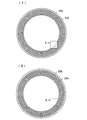
- (A) is a comparative example and (B) is an example of the present invention.
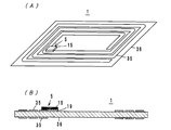
- the wireless communication device which is 1st Example is shown,
- (A) is a perspective view,
- (B) is sectional drawing.
- the antenna pattern which comprises 1st Example is shown,
- (A) is a front view,
- (B) is a back view.
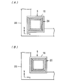
- positioning relationship of the feeder circuit board with respect to the antenna pattern in 1st Example is shown, (A) is sectional drawing, (B) is a top view which shows the arrangement
- FIG. 7 shows a wireless communication module according to a seventh embodiment, wherein (A) is a cross-sectional view, and (B) is a cross-sectional view showing a wireless communication device equipped with the wireless communication module.
- wireless communication device shown in FIG. 18 is shown, (A) is a front view, (B) is a back view.
- FIG. 1A shows a coupling state as a comparative example.
- a wireless communication device is roughly coupled to a wireless IC chip 10 for processing a wireless signal and the wireless IC chip 10, and coil patterns 21a to 21d have a predetermined width W1.
- the antenna pattern 35 that is magnetically coupled to the loop electrode 20 (which may be electromagnetic coupling, the same applies hereinafter). The specific shapes of the loop electrode 20 and the antenna pattern 35 will be described in detail in the first embodiment below.
- the loop electrode 20 is arranged so as not to overlap the antenna pattern 35 in plan view. Accordingly, the magnetic field ⁇ 1 due to the antenna pattern 35 is formed as indicated by a dotted line, and the magnetic field ⁇ 2 due to the loop electrode 20 is formed as indicated by a dashed line and is magnetically coupled to each other.
- a metal body is close to the lower side of the antenna pattern 35, a position where communication cannot be performed due to disturbance of the magnetic field, that is, a null point may be formed, and the communication distance may be shortened or communication may be poor.
- the auxiliary electrode 26 is provided on the feeder circuit board 15 so as to overlap the loop electrode 20 (coil patterns 21a to 21d) in plan view.
- the auxiliary electrode 26 is divided into a plurality of slits 26a (see FIG. 5).
- the loop electrode 20 is arranged so that at least a part of the winding width W1 of the coil patterns 21a to 21d overlaps the width W2 of the antenna pattern 35 when viewed in plan from the axial direction, and the auxiliary electrode 26 is also at least one.
- the portion is disposed so as to overlap the antenna pattern 35, and at least one slit 26 a is disposed so as not to overlap the antenna pattern 35.
- the loop electrode 20 and the antenna pattern 35 are magnetically coupled to transmit and receive a high frequency signal between the wireless IC chip 10 and the antenna pattern 35.
- the auxiliary electrode 26 and the antenna pattern 35 are magnetically coupled (which may be electromagnetic coupling, the same applies hereinafter), and high-frequency signals are transmitted and received between the wireless IC chip 10 and the antenna pattern 35. Since the auxiliary electrode 26 is formed with a slit 26a that divides the auxiliary electrode 26 into a plurality of parts, a potential difference occurs in the induced current generated in the auxiliary electrode 26, and the auxiliary electrode 26 and the antenna pattern 35 are coupled. Become.
- the auxiliary electrode 26 arranged so as to overlap the loop electrode 20 determines the magnetic field by the loop electrode 20 to some extent, and suppresses the disturbance of the magnetic field by the loop electrode 20 by the antenna pattern 35. Can do. As a result, even if the mounting position of the power feeding circuit board 15 with respect to the antenna pattern 35 is slightly deviated, the resonance frequency characteristics do not fluctuate, and the position accuracy of the power feeding circuit board is relaxed.
- the loop electrode 20 and the auxiliary electrode 26 are arranged so that at least a part thereof overlaps with the antenna pattern 35, the loop electrode 20 and the auxiliary electrode 26 and the antenna pattern 35 each have a magnetic field ⁇ 3 indicated by a dotted line. Even if a metal body is close to the lower side of the antenna pattern 35, at least the magnetic fields ⁇ 3a and ⁇ 3b are not disturbed, and there is no problem in coupling the two.
- the loop electrode 20 and the auxiliary electrode 26 are not connected in a DC manner, but are connected via a magnetic field and an electric field. However, it may be connected in a DC manner.
- the wireless communication device 1 As shown in FIG. 2, the wireless communication device 1 according to the first embodiment is used in the 13.56 MHz band, and is electrically connected to the wireless IC chip 10 that processes wireless signals and the wireless IC chip 10.
- the feeder circuit board 15 including the loop electrode 20 and the auxiliary electrode 26 (see FIGS. 4 and 5) in which the coil patterns 21a to 21d are wound with a predetermined width W1 (see FIG. 5), and the loop electrode 20 And an antenna pattern 35 magnetically coupled to the auxiliary electrode 26.
- a combination of the wireless IC chip 10 and the power supply circuit board 15 is referred to as a wireless communication module 5.
- the IC chip 10 includes a clock circuit, a logic circuit, a memory circuit, and the like, and necessary information is stored in the memory.
- input terminal electrodes and output terminal electrodes provided on the back surface thereof are electrically connected to both ends of the loop electrode 20.
- the antenna pattern 35 is formed by winding three turns in the shape of a coil on the front and back surfaces of a flexible base substrate 36 made of PET or the like, and both ends are opened.
- FIG. The antenna pattern 35 on the side is shown, and FIG. 3B shows the antenna pattern 35 on the back side as seen through from the front side.
- the antenna patterns 35 on the front and back sides have the same line width W2, are overlapped in a plan view and are capacitively coupled via the base substrate 36, and currents flow in the same direction.
- the antenna pattern 35 is formed of a metal material mainly composed of Ag, Cu or the like, and may be formed by patterning a metal film by a photolithography method or an etching method, or may be formed by screen printing a conductive paste. May be.
- the feeder circuit board 15 has a cavity 16 at the center, and the cavity 16 accommodates the wireless IC chip 10 and is filled with a sealing material 17. .
- the power supply circuit board 15 incorporates a loop electrode 20 and an auxiliary electrode 26 in which a plurality of coil patterns 21a to 21d are laminated in a multilayer manner.
- the auxiliary electrode 26 is disposed between the loop electrode 20 and the antenna pattern 35.
- a plurality of base material layers 18a to 18e are laminated, pressure-bonded, and fired as necessary.
- the base material layers 18a to 18e may be an insulator (dielectric material, magnetic material), a thermoplastic resin such as a liquid crystal polymer, or a thermosetting resin such as an epoxy polymer.
- an opening 25 is formed at the center, and a coil pattern 21a having pads 21a-1 and 21a-2 at both ends is formed.
- an opening 25 is formed at the center, and a coil pattern 21b and pads 22 having pads 21b-1 and 21b-2 are formed at both ends.
- an opening 25 is formed at the center, and a coil pattern 21c and pads 22 having pads 21c-1 and 21c-2 are formed at both ends.
- a coil pattern 21d and a land 23b having a land 23a at one end and a pad 21d-1 at the other end are formed on the fourth base layer 18d.
- An auxiliary electrode 26 is formed on the lowermost base material layer 18e.
- the auxiliary electrode 26 has a wide loop shape having the same inner periphery and outer periphery as the coil patterns 21a to 21d, and is divided into four equal areas by four slits 26a.
- These coil patterns, pads, lands, and auxiliary electrodes are made of a metal material mainly composed of Ag, Cu, etc., and may be formed by patterning a metal film by a photolithography method or an etching method, or may be conductive.
- the paste may be formed by screen printing.
- the pad 21d-1 of the coil pattern 21d is connected to the pad 21c-1 of the third layer coil pattern 21c via the interlayer conductor, and the coil pattern 21c.
- the end pad 21c-2 is connected to the pad 21b-1 of the second layer coil pattern 21b through an interlayer conductor.
- the other end pad 21b-2 of the coil pattern 21b is connected to the pad 21a-1 of the uppermost coil pattern 21a through an interlayer conductor.
- the other end pad 21 a-2 of the uppermost coil pattern 21 a is connected to a land 23 b provided on the lowermost layer via an interlayer conductor or pad 22.
- the opening 25 forms a cavity 16, and the wireless IC chip 10 accommodated in the cavity 16 has an input terminal electrode on the land 23b, an output terminal electrode on the land 23a, a solder bump 29 (see FIG. 4), etc. Connected with.
- the rectangular loop electrode 20 is formed in a plan view.
- the predetermined width W1 around which the coil patterns 21a to 21d are wound is a width from the inner peripheral pattern to the outer peripheral pattern.
- the current flows through the coil patterns 21a to 21d in the first direction indicated by the arrow x and in the second direction indicated by the arrow y opposite to the first direction. That is, each of the coil patterns 21a to 21d is wound so that a current flows in the same direction in a portion adjacent to the stacking direction.
- a region extending in the first direction x is referred to as a first region X
- a region extending in the second direction y is a second region Y. Called.
- the feeder circuit board 15 is disposed to face the inner corner portion of the antenna pattern 35 on the front surface (see FIG. 3A), and is attached with an insulating adhesive 19 (see FIG. 3). 6 (A)).
- the arrangement relationship in the vertical direction of the loop electrode 20 and the auxiliary electrode 26 with respect to the antenna pattern 35 is as shown in FIG. 6A.
- the first region X is arranged so as to overlap the antenna pattern 35, and the second region Y is The antenna pattern 35 is arranged so as not to overlap.
- the first direction x (the line length direction of the coil patterns 21a to 21d) and the line length direction of the antenna pattern 35 coincide with each other. As shown in FIG.
- the auxiliary electrode 26 is disposed so that two sides thereof overlap the antenna pattern 35, the two slits 26a overlap the antenna pattern 35, and the other two slits 26a are antenna patterns. 35 is arranged so as not to overlap. Further, the predetermined width W1 of the loop electrode 20 is preferably the same as or smaller than the width W3 of the auxiliary electrode 26 (see FIG. 5).
- the first region X of the loop electrode 20 is magnetically coupled to the antenna pattern 35. Further, the auxiliary electrode 26 and the antenna pattern 35 are magnetically coupled. Therefore, the high frequency signal radiated from the reader / writer of the RFID system and received by the antenna pattern 35 is supplied to the wireless IC chip 10 via the loop electrode 20 and the auxiliary electrode 26, and the wireless IC chip 10 operates. On the other hand, a response signal from the wireless IC chip 10 is transmitted to the antenna pattern 35 via the loop electrode 20 and the auxiliary electrode 26 and is radiated to the reader / writer.
- An LC resonance circuit is formed by the loop electrode 20 and the auxiliary electrode 26, and the frequency of the high-frequency signal transmitted from the antenna pattern 35 and the frequency of the high-frequency signal received by the antenna pattern 35 are substantially determined by this resonance frequency. Is done.
- a resonance circuit having a predetermined frequency is formed by the inductance component by the coil patterns 21a to 21d and the capacitance component between the lines, and an impedance matching circuit between the wireless IC chip 10 and the antenna pattern 35 is formed. Also works.
- the loop electrode 20 has its resonance frequency and impedance adjusted by adjusting its electrical length and pattern width.
- the auxiliary electrode 26 is formed with a slit 26a that divides the auxiliary electrode 26 into a plurality of parts, a potential difference is generated in the induced current generated in the auxiliary electrode 26, and the auxiliary electrode 26 and the antenna pattern 35 are coupled. It will be. As described above, the auxiliary electrode 26 disposed so as to overlap the loop electrode 20 can suppress the magnetic field generated by the loop electrode 20 from being disturbed by the antenna pattern 35. As a result, even if the mounting position of the power feeding circuit board 15 with respect to the antenna pattern 35 is slightly deviated, the resonance frequency characteristics do not fluctuate, and the position accuracy of the power feeding circuit board is relaxed.
- the first region X extending in the first direction x of the loop electrode 20 is disposed so as to overlap the antenna pattern 35 and is magnetically coupled. Even if the body is close, the magnetic field coupling between the loop electrode 20 and the antenna pattern 35 is maintained in the overlapping portion, and there is no problem in coupling the two.
- the arrangement of the feeder circuit board 15 in the directions of arrows a and b with respect to the antenna pattern 35 is such that the inner peripheral edge of the loop electrode 20 faces the inner peripheral edge of the antenna pattern 35.
- the auxiliary electrode 26 suppresses fluctuations in the inductance value due to the positional relationship between the loop electrode 20 and the antenna pattern 35, the coil patterns 21a to 21d are within this range where the loop electrode 20 and the antenna pattern 35 face each other. The inductance value does not fluctuate. Therefore, the positional accuracy of the feeder circuit board 15 is greatly relaxed.
- the first direction x (the line length direction of the coil patterns 21a to 21d) and the line length direction of the antenna pattern 35 coincide with each other, the current flows through the coil patterns 21a to 21d when transmitting a high-frequency signal.
- the induced current is guided to the antenna pattern 35 as an induced current in the line length direction, and high frequency power is efficiently transmitted.
- the line length directions of the coil patterns 21a to 21d and the antenna pattern 35 are not necessarily completely coincident with each other in the magnetic field coupling portion, and may be substantially coincident with each other. In other words, the line length directions of both need not be orthogonal.
- the feeder circuit board 15 is disposed to face the corner portion on the inner side of the antenna pattern 35, as shown in FIG. 6B, the third direction which is the direction with respect to the first direction of the loop electrode 20 is provided.
- the third region Z extending in the direction (see arrow z) also overlaps with the antenna pattern 35, and the third direction z and the line length direction of the antenna pattern 35 coincide.
- the loop electrode 20 and the antenna pattern 35 are magnetically coupled in the two regions of the first region X and the third region Z, and the degree of coupling between the two is increased.
- the feeder circuit board 15 has a substantially square shape in plan view, and the auxiliary electrode 26 has slits 26a formed at the center of four sides. If the feeder circuit board 15 has such a shape, when the feeder circuit board 15 is mounted on the antenna pattern 35, any of the four sides may be arranged along the antenna pattern 35. There is no question. On the other hand, when a plurality of slits 26 a are formed in the auxiliary electrode 26, if all the slits 26 a overlap the antenna pattern 35 in plan view, the induced current generated in the auxiliary electrode 26 circulates. In order to solve this problem, it is necessary that at least one slit 26 a does not overlap the antenna pattern 35.
- the width W3 of the auxiliary electrode 26 is preferably larger than the predetermined width W1 of the loop electrode 20. However, if the width W3 is too large, the substrate 15 is increased in size, and if it is overlapped so as to close the inner peripheral edge of the loop electrode 20, the inductance values of the coil patterns 21a to 21d tend to decrease. Absent.
- the sealing material 17 preferably contains a magnetic filler such as ferrite powder.
- a magnetic filler such as ferrite powder.
- the wireless communication module 5 can communicate with the reader / writer at a short distance without being combined with the antenna pattern 35.
- the loop electrode 20 and the auxiliary electrode 26 function as a radiating element.
- the wireless IC chip 10 for the power supply circuit board 15 adopts various mounting forms other than being housed in a cavity 16 provided on the surface of the board 15 and sealed with a sealing material 17. Can do.
- various embodiments of the wireless communication module in which the wireless IC chip is mounted on the power supply circuit board will be described.
- the wireless communication module 5A has a power supply circuit board 15 having a flat plate shape without a cavity, and the wireless IC chip 10 is mounted on a flat surface of the power supply circuit board 15. Although the height is increased by the thickness of the wireless IC chip 10, the step of forming a cavity in the substrate 15 can be omitted. In addition, there is an advantage that the number of turns of the loop electrode 20 is increased by forming a coil pattern in the portion where the cavity is formed.
- a wireless communication module 5B according to the third embodiment shown in FIG. 9 has a cavity 16 formed on the back surface of the feeder circuit board 15 to accommodate the wireless IC chip 10 and sealed with a sealing material 17. Further, the auxiliary electrode 26 and the loop electrode 20 are electrically connected (DC connection) by an interlayer conductor 27. Note that sealing with the sealing material 17 is not always necessary. This is because the wireless IC chip 10 accommodated in the cavity 16 is protected by sticking the back surface of the power supply circuit board 15 to the base film 36.
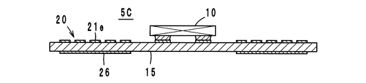
- the wireless communication module 5C according to the fourth embodiment shown in FIG. 10 is provided with the coil pattern 21e on the surface of the feeder circuit board 15 to form the loop electrode 20, and the auxiliary electrode 26 is formed on the back surface of the board 15.
- the wireless IC chip 10 is mounted on the surface of the substrate 15.
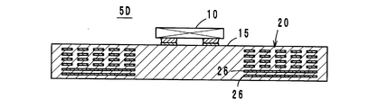
- a wireless communication module 5D according to the fifth embodiment shown in FIG. 11 has the feeder circuit board 15 provided with the auxiliary electrode 26 in two layers, and the auxiliary electrode 26 may be provided in two or more layers.
- the auxiliary electrode 26 of each layer may be electrically independent or connected. When the auxiliary electrodes 26 of each layer are electrically connected, it is preferable that the directions of the currents flowing through the auxiliary electrodes 26 are the same.
- the wireless communication module 5E according to the sixth embodiment shown in FIG. 12 is provided with the auxiliary electrode 26 on the feeder circuit board 15 so as to sandwich the loop electrode 20 in two layers.
- the lower auxiliary electrode 26 has a function of suppressing the resonance frequency from being fluctuated by a metal body close to the lower side of the feeder circuit board 15.
- the upper auxiliary electrode 26 has a function of suppressing the resonance frequency from being fluctuated by a metal body close to the upper side of the feeder circuit board 15.
- FIGS. 6B and 6C various forms can be adopted as the mounting form of the feeder circuit board 15 with respect to the antenna pattern 35 other than the mounting on the corner portion of the antenna pattern 35.
- the line length directions of the loop electrodes 20 (coil patterns 21a to 21d) and the antenna pattern 35 are not necessarily arranged so as to coincide with each other in the magnetic field coupling portion. As long as it flows.
- one side of the auxiliary electrode 26 (the first region X of the loop electrode 20) is mounted so as to overlap the linear portion of the antenna pattern 35.
- the power feeding circuit board 15 is displaced in the line length direction (see arrow a) of the antenna pattern 35, the frequency characteristics do not change.
- the area of the portion where the loop electrode 20 (coil patterns 21a to 21d) is orthogonal to the line length direction of the antenna pattern 35 and overlaps the antenna pattern 35 is smaller.
- a bent portion 35a is formed in the antenna pattern 35, and the three sides of the auxiliary electrode 26 (the loop electrode 20) are superimposed on the bent portion 35a.
- the degree of coupling increases as the overlapping area between each of the auxiliary electrode 26 and the loop electrode 20 and the antenna pattern 35 increases.
- the feeder circuit board 15 is arranged at the inner corner of the antenna pattern 35 as in FIGS. 6B and 6C, but the auxiliary electrode 26 has one slit. Only 26a is formed. The slit 26 a is arranged so as not to overlap the antenna pattern 35.
- the wireless communication module 5F according to the seventh embodiment is formed such that the cavity portion 16 is formed in the feeder circuit board 15 so as to open on the back side of the substrate 15 and the cavity portion 16 is wirelessly connected.
- the IC chip 10 is accommodated and the sealing material 17 is filled.
- Other configurations are the same as those of the first embodiment.
- the wireless communication module 5F is attached to the base substrate 36 with an insulating adhesive 19 with the opening of the cavity 16 facing the base substrate 36.
- the wireless communication device 1A is arranged in FIG. 17A.
- the effects of the wireless communication module 5F and the wireless communication device 1A are basically the same as those shown in FIG. 2, and in particular, the bottom surface of the cavity portion 16 (disposed on the top surface in FIG. 17A).
- the wireless IC chip 10 is protected.
- the bottom surface of the power supply circuit board 15 (which is the top surface in FIG. 10A) has high flatness, suction when the wireless communication module 5F is mounted on the base substrate 36 by vacuum suction using a mounter. Good performance.
- FIG. 17A since the sealing material 17 slightly protrudes from the cavity portion 16, the protruding portion is not mounted when mounted on the base substrate 36 (when bonded with the adhesive 19). The anchor effect is exhibited, and the feeder circuit board 15 is firmly bonded onto the base substrate 36. In addition, even if the sealing material 17 has a concave shape on the contrary, the anchor effect is exhibited.
- FIGS. 18 to 20 Next, a third example of a wireless communication device equipped with the wireless communication module 5 will be described.
- the wireless communication device 1B is obtained by mounting the wireless communication module 5 on a flexible base substrate 36A having a circular shape, and on the front and back surfaces of the base substrate 36A, as shown in FIG.
- An antenna pattern 35A as a second example shown in (B) is formed. Note that the antenna pattern 35A on the back surface side shown in FIG. 19B is seen through from the front surface side.
- the antenna patterns 35A are wound in a circular shape, overlap each other in plan view over almost the entire length, and are capacitively coupled to each other.
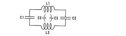
- the antenna pattern 35A forms the equivalent circuit shown in FIG.
- Capacitance C3 is generated between the front and back patterns which are coupled by the capacitance C2.
- the operation of the antenna pattern 35A capacitively coupled to each other is the same as that of the antenna pattern 35 shown in FIG. 2, and the current flows in the same direction.
- the coiled electrode 20 of the wireless communication module 5 disposed on the surface of the base substrate 36A and partially overlapping the antenna pattern 35A is magnetically coupled to the antenna pattern 35A. Therefore, the reader / writer antenna and the wireless communication module 5 can communicate with each other via the antenna pattern 35A.
- the basic operational effects of the wireless communication device 1B are as described in the wireless communication device 1.
- both end portions of the antenna pattern 35A arranged on the front and back sides of the base substrate 36A may be DC coupled by crimping (pouching). May be combined. In short, it is only necessary that the directions of the currents flowing through the antenna patterns 35A on the front and back sides are the same.
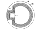
- FIG. 21 shows an antenna pattern 35B as a third example.
- the antenna pattern 35B has a substantially circular shape having a rectangular portion 35B ′, is formed on the front and back surfaces of the base substrate 36A, and the antenna pattern on the back surface side is formed so as to overlap the antenna pattern 35B on the front surface side in plan view. Yes.
- the antenna patterns 35B on the front and back surfaces are capacitively coupled to each other, and the equivalent circuit thereof is the same as in FIG.
- the wireless communication module 5 is mounted along the inner peripheral portion of the rectangular portion 35B ′ on the surface side of the base substrate 36A, and the coiled electrode 20 built in the wireless communication module 5 is connected to the antenna pattern 35B and the magnetic field. Combine to form a wireless communication device.
- the operational effects of the antenna pattern 35B are as described for the antenna pattern 35A.
- the antenna pattern 35B is coupled to the coiled electrode 20 at three sides, and the amount of coupling between the antenna pattern 35B and the coiled electrode 20 is increased.
- FIG. 22 shows an antenna pattern 35C as a fourth example.
- the antenna pattern 35C has a substantially circular shape having a stepped portion 35C ′, is formed on the front and back surfaces of the base substrate 36A, and the antenna pattern on the back surface side is formed so as to overlap the antenna pattern 35C on the front surface side in plan view. ing.
- the antenna patterns 35C on the front and back surfaces are capacitively coupled to each other, and an equivalent circuit thereof is the same as that in FIG.
- the wireless communication module 5 is mounted on the surface side of the base substrate 36A along the inner peripheral portion of the stepped portion 35C ′, and the coiled electrode 20 is magnetically coupled to the antenna pattern 35C to constitute a wireless communication device. To do.
- the operational effects of the antenna pattern 35C are as described for the antenna pattern 35A.
- the antenna pattern 35C is coupled to the coiled electrode 20 at two sides, and the amount of coupling between the antenna pattern 35C and the coiled electrode 20 is increased.
- FIG. 23 shows an antenna pattern 35D as a fifth example.
- the antenna pattern 35D is basically arranged in the same shape as the antenna pattern 35A shown in FIG. 19, and the outermost turn portion 35D ′ is formed thicker than the other portions. Other configurations and operational effects are basically the same as described in the antenna pattern 35A.
- the coupling capacitance value at the outermost turn portion 35D ′ increases, the resonance frequency of the antenna pattern 35D can be lowered.
- the magnetic flux passage region can be increased without reducing the opening diameter. That is, in the antenna pattern 35D, the resonance frequency can be shifted to the lower side, and the communication distance can be maintained and improved without increasing the overall size.
- FIG. 24 shows an antenna pattern 35E as a sixth example.
- the antenna pattern 35E has the outermost turn portion 35E ′ thick as in the antenna pattern 35D shown in FIG. 25.
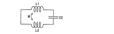
- the antenna pattern 35E forms the equivalent circuit shown in FIG. 25, and the inductor L1 formed by the antenna pattern 35E on the front surface side and the inductor L2 formed by the antenna pattern 35E on the back surface side are magnetically coupled to each other.
- one end 35E ′′ is coupled in a direct current manner, and the outermost turn portions 35E ′′ are coupled by a capacitor C2.
- the operation of the antenna patterns 35E magnetically coupled to each other is the same as that of the antenna pattern 35A shown in FIG.
- the coupling capacitance value at the outermost turn portion 35E ' is increased, so that the resonance frequency of the antenna pattern 35E can be lowered.
- the magnetic flux passage area can be increased without reducing the opening diameter. That is, in the antenna pattern 35E, the resonance frequency can be shifted to the lower side, and the communication distance can be maintained and improved without increasing the overall size.
- FIG. 26 As an example of a wireless communication terminal according to the present invention, an IC card 50 is shown in FIG.
- the IC card 50 has the wireless communication device 1 incorporated therein.
- the wireless communication module, the wireless communication device, and the wireless communication terminal according to the present invention are not limited to the above-described embodiments, and can be variously modified within the scope of the gist.
- the auxiliary electrode is disposed so as to overlap substantially the entire area of the loop electrode, but the auxiliary electrode may be disposed at a position where the loop electrode overlaps with the antenna pattern.
- the loop electrode has a predetermined width by winding the coil pattern a plurality of turns, but may be wound by one turn to have a predetermined width.
- the coil pattern may be wound in a single layer without being wound in multiple layers.
- the wireless IC may be formed integrally with the inside of the power supply circuit board other than the chip mounted on the power supply circuit board.
- the wireless IC may be mounted as a chip on another substrate disposed in the vicinity of the power supply circuit substrate.
- the wireless communication device can be mounted on various portable products.
- the wireless IC chip and the loop electrode may not be DC-connected (directly connected), and may be coupled via an electromagnetic field. In other words, it only needs to be electrically connected.
- the antenna pattern may have various shapes as long as it plays a role as an antenna. Further, the present invention is not limited to the HF band such as the 13.56 MHz band, and can be used for a UHF band or a SHF band wireless communication device.
- the present invention is useful for a wireless communication module, a wireless communication device, and a wireless communication terminal, and is particularly excellent in that the positional accuracy of the feeder circuit board with respect to the antenna pattern is relaxed and the production efficiency is increased.
Landscapes
- Engineering & Computer Science (AREA)
- Physics & Mathematics (AREA)
- Electromagnetism (AREA)
- Toxicology (AREA)
- Microelectronics & Electronic Packaging (AREA)
- Health & Medical Sciences (AREA)
- Computer Networks & Wireless Communication (AREA)
- General Physics & Mathematics (AREA)
- Theoretical Computer Science (AREA)
- General Health & Medical Sciences (AREA)
- Artificial Intelligence (AREA)
- Computer Vision & Pattern Recognition (AREA)
- Computer Hardware Design (AREA)
- Details Of Aerials (AREA)
- Support Of Aerials (AREA)
Abstract
アンテナパターンに対する給電回路基板の位置精度を緩和し、生産効率を高めることのできる無線通信モジュール、無線通信デバイス及び無線通信端末を得る。 無線信号を処理する無線ICチップ10と、無線ICチップ10に電気的に接続されたループ状電極20及び補助電極20を含む給電回路基板15と、ループ状電極20及び補助電極26と電磁界結合されたアンテナパターン35と、を備えた無線通信デバイス。ループ状電極20はコイルパターンを巻回してなり、平面視で、少なくとも一部がアンテナパターン35と重なるように配置されている。補助電極26は、平面視で、少なくとも一部がループ状電極20及びアンテナパターン35と重なるように配置されている。補助電極26には少なくとも一つの分割用スリットが形成され、該スリットの少なくとも一つはアンテナパターン35とは重ならないように配置されている。
Description
本発明は、無線通信モジュール、無線通信デバイス及び無線通信端末、特にRFID(Radio Frequency Identification)システムに用いられる無線通信モジュール、無線通信デバイス及び無線通信端末に関する。
近年、物品の情報管理システムとして、誘導磁界を発生するリーダライタと、物品に付されたRFIDタグ(無線通信デバイスとも称する)とを電磁界を利用した非接触方式で通信し、所定の情報を伝達するRFIDシステムが実用化されている。RFIDタグは、所定の情報を記憶し、所定の無線信号を処理する無線ICと、高周波信号の送受信を行うアンテナとを備えている。
特許文献1には、RFIDシステムに用いられる無線ICデバイスが記載されている。この無線ICデバイスは、無線ICチップを搭載した給電回路基板を有し、この給電回路基板を放射板(アンテナパターン)に主に磁界結合させている。この無線ICデバイスでは、給電回路基板に内蔵されている給電回路にて送受信信号の周波数が決められているため、動作周波数はアンテナパターンのサイズ、デバイスの保持部材の材質などに依存することなく安定した周波数特性を有する。
ところで、特許文献1に記載の給電回路は、インダクタンス素子やキャパシタンス素子にて構成されており、インダクタンス素子とアンテナパターンとを磁界結合させて高周波信号を送受している。しかし、アンテナパターンに対する給電回路基板の搭載位置がずれると、インダクタンス素子による磁界が乱れて、インダクタンス素子の共振周波数特性が変動してしまう。それゆえ、給電回路基板には高い位置精度が求められており、生産効率の低下を招いていた。
そこで、本発明の目的は、アンテナパターンに対する給電回路基板の位置精度を緩和し、生産効率を高めることができる無線通信モジュール、無線通信デバイス及び無線通信端末を提供することにある。
本発明の第1の形態である無線通信モジュールは、
無線信号を処理する無線ICと、
前記無線ICに結合されたループ状電極及び補助電極を含む給電回路基板と、
を備え、
前記ループ状電極はコイルパターンを巻回してなり、
前記補助電極は、コイル軸方向から平面視したとき、前記ループ状電極の少なくとも一部と重なるように配置され、少なくとも一部に該補助電極を複数に分割するスリットが形成されていること、
を特徴とする。
無線信号を処理する無線ICと、
前記無線ICに結合されたループ状電極及び補助電極を含む給電回路基板と、
を備え、
前記ループ状電極はコイルパターンを巻回してなり、
前記補助電極は、コイル軸方向から平面視したとき、前記ループ状電極の少なくとも一部と重なるように配置され、少なくとも一部に該補助電極を複数に分割するスリットが形成されていること、
を特徴とする。
本発明の第2の形態である無線通信デバイスは、
無線信号を処理する無線ICと、
前記無線ICに結合されたループ状電極及び補助電極を含む給電回路基板と、
前記ループ状電極及び前記補助電極と結合されたアンテナパターンと、
を備え、
前記ループ状電極はコイルパターンを巻回してなり、
前記補助電極は、コイル軸方向から平面視したとき、前記ループ状電極の少なくとも一部と重なるように配置され、少なくとも一部に該補助電極を複数に分割するスリットが形成されており、
前記ループ状電極は、コイル軸方向から平面視したとき、少なくとも一部が前記アンテナパターンと重なるように配置されており、
前記補助電極は、コイル軸方向から平面視したとき、少なくとも一部が前記ループ状電極及び前記アンテナパターンと重なるように配置され、かつ、少なくとも一つの前記スリットが前記アンテナパターンとは重ならないように配置されていること、
を特徴とする。
無線信号を処理する無線ICと、
前記無線ICに結合されたループ状電極及び補助電極を含む給電回路基板と、
前記ループ状電極及び前記補助電極と結合されたアンテナパターンと、
を備え、
前記ループ状電極はコイルパターンを巻回してなり、
前記補助電極は、コイル軸方向から平面視したとき、前記ループ状電極の少なくとも一部と重なるように配置され、少なくとも一部に該補助電極を複数に分割するスリットが形成されており、
前記ループ状電極は、コイル軸方向から平面視したとき、少なくとも一部が前記アンテナパターンと重なるように配置されており、
前記補助電極は、コイル軸方向から平面視したとき、少なくとも一部が前記ループ状電極及び前記アンテナパターンと重なるように配置され、かつ、少なくとも一つの前記スリットが前記アンテナパターンとは重ならないように配置されていること、
を特徴とする。
本発明の第3の形態である無線通信端末は、前記無線通信デバイスを備えたことを特徴とする。
前記無線通信デバイスにおいて、コイルパターンを巻回してなるループ状電極とアンテナパターンとが磁界結合し、さらに、補助電極とアンテナパターンとが磁界結合する。そして、ループ状電極及び補助電極を介して、無線ICとアンテナパターンとの間で高周波信号を送受信する。補助電極には該補助電極を複数に分割するスリットが形成されているため、補助電極に生じた誘導電流には電位差が生じ、補助電極とアンテナパターンとが結合することになる。このように、ループ状電極と重なるように配置された補助電極によって、ループ状電極による磁界がアンテナパターンによって乱されることを抑制することができる。この結果、アンテナパターンに対する給電回路基板の搭載位置が多少ずれたとしても共振周波数特性が変動することはなく、給電回路基板の位置精度が緩和される。
本発明によれば、アンテナパターンに対する給電回路基板の位置精度が緩和され、生産効率を高めることができる。
以下、本発明に係る無線通信モジュール、無線通信デバイス及び無線通信端末の実施例について添付図面を参照して説明する。なお、各図において、共通する部品、部分は同じ符号を付し、重複する説明は省略する。
(原理的説明、図1参照)
本発明に係る無線通信デバイスにおける、ループ状電極及び補助電極のそれぞれとアンテナパターンとの結合状態について原理的に説明する。
本発明に係る無線通信デバイスにおける、ループ状電極及び補助電極のそれぞれとアンテナパターンとの結合状態について原理的に説明する。
図1(A)は比較例としての結合状態を示し、無線通信デバイスは、概略、無線信号を処理する無線ICチップ10と、無線ICチップ10に結合され、コイルパターン21a~21dが所定幅W1で巻回されてなるループ状電極20を含む給電回路基板15と、ループ状電極20と磁界結合(電磁界結合であってもよい、以下同じ)されたアンテナパターン35と、を備えている。なお、ループ状電極20やアンテナパターン35の具体的な形状は以下に第1実施例で詳述する。
図1(A)では、アンテナパターン35に対してループ状電極20が平面視で重ならないように配置されている。従って、アンテナパターン35による磁界φ1は点線で示すように形成され、ループ状電極20による磁界φ2は一点鎖線で示すように形成され、互いに磁界結合している。しかし、アンテナパターン35の下方に金属体が近接すると、磁界が乱れて通信ができない位置、即ち、ヌル点ができることがあり、通信距離が短くなったり、通信が不良になることがある。
以上の比較例に対して、図1(B)に示す本発明例においては、給電回路基板15に、ループ状電極20(コイルパターン21a~21d)と平面視で重なるように補助電極26を設けており、補助電極26はスリット26a(図5参照)にて複数に分割されている。そして、ループ状電極20はその軸方向から平面視したとき、コイルパターン21a~21dの巻回幅W1の少なくとも一部がアンテナパターン35の幅W2に重なるように配置され、補助電極26も少なくとも一部がアンテナパターン35と重なるように配置され、かつ、少なくとも一つのスリット26aがアンテナパターン35とは重ならないように配置されている。
本発明例において、ループ状電極20とアンテナパターン35とが磁界結合し、無線ICチップ10とアンテナパターン35との間で高周波信号を送受信する。さらに、補助電極26とアンテナパターン35とが磁界結合(電磁界結合であってもよい、以下同じ)し、無線ICチップ10とアンテナパターン35との間で高周波信号を送受信する。補助電極26には該補助電極26を複数に分割するスリット26aが形成されているため、補助電極26に生じた誘導電流には電位差が生じ、補助電極26とアンテナパターン35とが結合することになる。このように、ループ状電極20と重なるように配置された補助電極26によって、ループ状電極20による磁界がある程度決定され、ループ状電極20による磁界がアンテナパターン35によって乱されることを抑制することができる。この結果、アンテナパターン35に対する給電回路基板15の搭載位置が多少ずれたとしても共振周波数特性が変動することはなく、給電回路基板の位置精度が緩和される。
また、ループ状電極20及び補助電極26はそれぞれ少なくとも一部がアンテナパターン35と重なるように配置されているため、ループ状電極20及び補助電極26のそれぞれとアンテナパターン35とは点線で示す磁界φ3で結合されており、仮にアンテナパターン35の下方に金属体が近接しても、少なくとも磁界φ3a,φ3bは乱されることがなく、両者の結合に支障が生じることはない。なお、本発明例において、ループ状電極20と補助電極26とはDC的には接続されていないが、磁界及び電界を介して接続されている。但し、DC的に接続されていても構わない。
(第1実施例、無線通信デバイス、図2~図7参照)
図2に示すように、第1実施例である無線通信デバイス1は13.56MHz帯に使用されるものであり、無線信号を処理する無線ICチップ10と、無線ICチップ10に電気的に接続され、コイルパターン21a~21dが所定幅W1(図5参照)で巻回されてなるループ状電極20及び補助電極26(図4及び図5参照)を含む給電回路基板15と、ループ状電極20及び補助電極26と磁界結合されたアンテナパターン35と、を備えている。ここで、無線ICチップ10と給電回路基板15を組み合わせたものを無線通信モジュール5と称する。ICチップ10は、クロック回路、ロジック回路、メモリ回路などを含み、必要な情報がメモリされている。無線ICチップ10は、その裏面に設けた入力用端子電極及び出力用端子電極をループ状電極20の両端に電気的に接続されている。
図2に示すように、第1実施例である無線通信デバイス1は13.56MHz帯に使用されるものであり、無線信号を処理する無線ICチップ10と、無線ICチップ10に電気的に接続され、コイルパターン21a~21dが所定幅W1(図5参照)で巻回されてなるループ状電極20及び補助電極26(図4及び図5参照)を含む給電回路基板15と、ループ状電極20及び補助電極26と磁界結合されたアンテナパターン35と、を備えている。ここで、無線ICチップ10と給電回路基板15を組み合わせたものを無線通信モジュール5と称する。ICチップ10は、クロック回路、ロジック回路、メモリ回路などを含み、必要な情報がメモリされている。無線ICチップ10は、その裏面に設けた入力用端子電極及び出力用端子電極をループ状電極20の両端に電気的に接続されている。
アンテナパターン35は、PETなどからなる可撓性ベース基材36の表面及び裏面にコイル状に3ターン巻回され、かつ、両端が開放状態で形成されたもので、図3(A)は表面側のアンテナパターン35を示し、図3(B)は裏面側のアンテナパターン35を表面側から透視した状態で示している。表裏のアンテナパターン35は、線幅W2が同じであり、平面視で重なってベース基材36を介して容量結合しており、電流は同じ方向に流れる。アンテナパターン35は、Ag,Cuなどを主成分とする金属材料で形成され、金属膜をフォトリソ法やエッチング法によってパターニングして形成してもよく、あるいは、導電性ペーストをスクリーン印刷して形成してもよい。
給電回路基板15は多層基板であって、図4に示すように、中央部にキャビティ16を有し、該キャビティ16には前記無線ICチップ10が収容され、封止材17が充填されている。給電回路基板15には複数のコイルパターン21a~21dを多層に積層したループ状電極20及び補助電極26が内蔵されている。補助電極26はループ状電極20とアンテナパターン35との間に配置されている。具体的には、図5に示すように、複数の基材層18a~18eを積層、圧着、必要に応じて焼成したものである。基材層18a~18eは、絶縁体(誘電体、磁性体)あるいは液晶ポリマなどのような熱可塑性樹脂やエポキシ系ポリマなどのような熱硬化性樹脂であってもよい。
最上層の基材層18aには、中央に開口部25が形成され、両端にパッド21a-1,21a-2を有するコイルパターン21aが形成されている。2層目の基材層18bには、中央に開口部25が形成され、両端にパッド21b-1,21b-2を有するコイルパターン21b及びパッド22が形成されている。3層目の基材層18cには、中央に開口部25が形成され、両端にパッド21c-1,21c-2を有するコイルパターン21c及びパッド22が形成されている。4層目の基材層18dには、一端にランド23aを有し他端にパッド21d-1を有するコイルパターン21d及びランド23bが形成されている。最下層の基材層18eには補助電極26が形成されている。この補助電極26は前記コイルパターン21a~21dと同じ内周及び外周を有する幅広のループ状であり、4本のスリット26aによって等しい面積に4分割されている。これらのコイルパターンやパッド、ランド及び補助電極は、Ag,Cuなどを主成分とする金属材料で形成され、金属膜をフォトリソ法やエッチング法によってパターニングして形成してもよく、あるいは、導電性ペーストをスクリーン印刷して形成してもよい。
以上の基材層18a~18eを積層することにより、コイルパターン21dはパッド21d-1が層間導体を介して3層目のコイルパターン21cのパッド21c-1に接続され、該コイルパターン21cの他端パッド21c-2は層間導体を介して2層目のコイルパターン21bのパッド21b-1に接続される。該コイルパターン21bの他端パッド21b-2は層間導体を介して最上層のコイルパターン21aのパッド21a-1に接続される。また、最上層のコイルパターン21aの他端パッド21a-2は層間導体やパッド22を介して最下層に設けたランド23bに接続される。
開口部25はキャビティ16を形成し、該キャビティ16に収容された無線ICチップ10は入力用端子電極がランド23bに、出力用端子電極がランド23aに、それぞれはんだバンプ29(図4参照)などで接続される。
以上のごとくコイルパターン21a~21dが巻回されることにより、平面視で矩形状のループ状電極20が形成される。コイルパターン21a~21dが巻回されている所定幅W1とは内周側のパターンから外周側のパターンまでの幅である。ランド23aから電流が供給されると、該電流は各コイルパターン21a~21dを矢印xで示す第1の方向及び第1の方向とは反対方向の矢印yで示す第2の方向に流れる。即ち、各コイルパターン21a~21dは、積層方向に隣接する部分では、同方向に電流が流れるように巻回されている。図5において、コイル軸方向から平面視したとき、第1の方向xに延在している領域を第1領域Xと称し、第2の方向yに延在している領域を第2領域Yと称する。
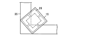
本第1実施例において、給電回路基板15は表面のアンテナパターン35の内側のコーナー部に対向して配置され(図3(A)参照)、絶縁性の接着剤19で貼着される(図6(A)参照)。アンテナパターン35に対するループ状電極20及び補助電極26の垂直方向の配置関係は図6(A)に示すとおりであり、第1領域Xがアンテナパターン35に重なるように配置され、第2領域Yはアンテナパターン35に重ならないように配置されている。また、図6(B)に示すように、第1の方向x(コイルパターン21a~21dの線路長方向)とアンテナパターン35の線路長方向とが一致している。補助電極26は、図6(C)に示すように、2辺がアンテナパターン35と重なるように配置され、かつ、二つのスリット26aがアンテナパターン35と重なり、他の二つのスリット26aはアンテナパターン35とは重ならないように配置されている。また、ループ状電極20の所定幅W1は補助電極26の幅W3(図5参照)と同じか、幅W3よりも小さいことが好ましい。
以上の構成からなる無線通信デバイス1において、ループ状電極20の第1領域Xがアンテナパターン35と磁界結合している。さらに、補助電極26とアンテナパターン35とが磁界結合している。それゆえ、RFIDシステムのリーダライタから放射されてアンテナパターン35で受信された高周波信号がループ状電極20及び補助電極26を介して無線ICチップ10に供給され、無線ICチップ10が動作する。一方、無線ICチップ10からの応答信号がループ状電極20及び補助電極26を介してアンテナパターン35に伝達されてリーダライタに放射される。
ループ状電極20及び補助電極26によってLC共振回路が形成され、この共振周波数によって、アンテナパターン35から送信される高周波信号の周波数、及び、アンテナパターン35で受信する高周波信号の周波数が実質的に決定される。ループ状電極20単独では、それぞれのコイルパターン21a~21dによるインダクタンス成分と線間のキャパシタンス成分とで所定周波数の共振回路を形成し、かつ、無線ICチップ10とアンテナパターン35とのインピーダンスの整合回路としても機能する。ループ状電極20はその電気長やパターン幅などを調整することで、共振周波数やインピーダンスが調整される。
また、補助電極26には該補助電極26を複数に分割するスリット26aが形成されているため、補助電極26に生じた誘導電流には電位差が生じ、補助電極26とアンテナパターン35とが結合することになる。このように、ループ状電極20と重なるように配置された補助電極26によって、ループ状電極20による磁界がアンテナパターン35によって乱されることを抑制することができる。この結果、アンテナパターン35に対する給電回路基板15の搭載位置が多少ずれたとしても共振周波数特性が変動することはなく、給電回路基板の位置精度が緩和される。
前記無線通信デバイス1においては、ループ状電極20の第1の方向xに延在している第1領域Xがアンテナパターン35に重なるように配置されて磁界結合しているため、仮に他の金属体が近接したとしても、ループ状電極20とアンテナパターン35との磁界結合が重なり部分では保たれ、両者の結合に支障が生じることはない。
図7(A),(B)に示すように、給電回路基板15のアンテナパターン35に対する矢印a,b方向の配置は、ループ状電極20の内周縁がアンテナパターン35の内周縁に対向する位置から、ループ状電極20の外周縁がアンテナパターン35の内周縁に対応する位置までの範囲内に収めればよい。補助電極26によって、ループ状電極20とアンテナパターン35との位置関係によるインダクタンス値の変動を抑制しているので、ループ状電極20とアンテナパターン35が対向するこの範囲内において、コイルパターン21a~21dのインダクタンス値が変動しない。従って、給電回路基板15の位置精度は大きく緩和されることになる。
また、第1の方向x(コイルパターン21a~21dの線路長方向)とアンテナパターン35の線路長方向とが一致しているため、高周波信号の送信時であれば、コイルパターン21a~21dに流れた電流がアンテナパターン35にその線路長方向に誘導電流として導かれ、高周波電力が効率よく伝送される。なお、磁界結合部分においてコイルパターン21a~21d及びアンテナパターン35の線路長方向は必ずしも完全に一致している必要はなく、略一致していればよい。換言すれば、両者の線路長方向は直交していなければよい。
また、給電回路基板15がアンテナパターン35の内側のコーナー部に対向して配置されているため、図6(B)に示すように、ループ状電極20の第1の方向に対する方向である第3の方向(矢印z参照)に延在している第3領域Zもアンテナパターン35と重なるようになり、第3の方向zとアンテナパターン35の線路長方向とが一致している。これにて、第1領域Xと第3領域Zの二つの領域で、ループ状電極20とアンテナパターン35とが磁界結合することになり、両者の結合度が強くなる。
さらに、本第1実施例においては、給電回路基板15が平面視で略正方形状であり、補助電極26には4辺の中央部にスリット26aが形成されている。給電回路基板15がこのような形状であれば、給電回路基板15をアンテナパターン35に搭載する際、4辺のいずれをアンテナパターン35に沿わせて配置してもよく、搭載時の方向性を問うことはない。一方、補助電極26に複数のスリット26aが形成されている場合、平面視で全てのスリット26aがアンテナパターン35と重なると、補助電極26に生じる誘導電流が周回してしまう。これを解消するために、少なくとも一つのスリット26aがアンテナパターン35と重なっていないことが必要である。補助電極26の幅W3はループ状電極20の所定幅W1よりも大きいことが好ましい。しかし、幅W3があまり大きくなると、基板15の大型化を招くほか、ループ状電極20の内周縁を塞ぐように重なると、コイルパターン21a~21dのインダクタンス値が低下する傾向にあり、好ましいことではない。
また、本第1実施例において、封止材17はフェライト粉末のような磁性体フィラーを含有していることが好ましい。これにより、無線ICチップ10からの輻射ノイズを低減できるとともに、コイルパターン21a~21dのインダクタンス値を大きくすることができる。インダクタンス値を大きくするという点で、前述したように、キャビティ16を深くすることが好ましい。
なお、無線通信モジュール5は、前記アンテナパターン35と組み合わせることなく、単独でもリーダライタと近距離ではあるが通信が可能である。この場合は、ループ状電極20及び補助電極26が放射素子として機能する。
(無線通信モジュールの各種実施例、図8~図12参照)
給電回路基板15に対する無線ICチップ10は、図4に示したように、基板15の表面に設けたキャビティ16に収容して封止材17で封止する以外に種々の搭載形態を採用することができる。ここで、無線ICチップを給電回路基板に搭載した無線通信モジュールの種々の実施例について説明する。
給電回路基板15に対する無線ICチップ10は、図4に示したように、基板15の表面に設けたキャビティ16に収容して封止材17で封止する以外に種々の搭載形態を採用することができる。ここで、無線ICチップを給電回路基板に搭載した無線通信モジュールの種々の実施例について説明する。
図8に示す第2実施例である無線通信モジュール5Aは、給電回路基板15をキャビティのない平板状とし、無線ICチップ10を給電回路基板15の平坦な表面上に搭載したものである。無線ICチップ10の厚み分だけ背が高くなるが、基板15にキャビティを形成する工程を省略することができる。また、キャビティが形成される部分にコイルパターンを形成してループ状電極20のターン数を増加させるなどの利点を有する。
図9に示す第3実施例である無線通信モジュール5Bは、給電回路基板15の裏面にキャビティ16を形成して無線ICチップ10を収容し、封止材17で封止したものである。さらに、補助電極26とループ状電極20とは層間導体27によって電気的に接続(DC接続)されている。なお、封止材17での封止は必ずしも必要ではない。キャビティ16に収容された無線ICチップ10は、給電回路基板15の裏面がベースフィルム36に貼着されることで保護されるからである。
図10に示す第4実施例である無線通信モジュール5Cは、コイルパターン21eを給電回路基板15の表面に設けてループ状電極20を形成するとともに、基板15の裏面に補助電極26を形成し、無線ICチップ10を基板15の表面上に搭載したものである。
図11に示す第5実施例である無線通信モジュール5Dは、給電回路基板15に補助電極26を2層に設けたものであり、補助電極26は2層以上の複数層に設けてもよい。各層の補助電極26は電気的に独立していてもよいし、接続されていてもよい。各層の補助電極26を電気的に接続する際には、各補助電極26に流れる電流の向きが同方向になることが好ましい。
図12に示す第6実施例である無線通信モジュール5Eは、給電回路基板15に補助電極26を、2層にかつループ状電極20を上下に挟み込むように設けたものである。下側の補助電極26は給電回路基板15の下方に近接する金属体によって共振周波数が変動することを抑制する機能を有する。上側の補助電極26は給電回路基板15の上方に近接する金属体によって共振周波数が変動することを抑制する機能を有する。
(給電回路基板の他の搭載形態、図13~図16参照)
アンテナパターン35に対する給電回路基板15の搭載形態は、図6(B),(C)に示したように、アンテナパターン35のコーナー部に搭載する以外に種々の形態を採用することができる。特に、磁界結合部分においてループ状電極20(コイルパターン21a~21d)及びアンテナパターン35の線路長方向は必ずしも一致するように配置されている必要はなく、一方から他方へと線路長方向に誘導電流が流れるように配置されていればよい。
アンテナパターン35に対する給電回路基板15の搭載形態は、図6(B),(C)に示したように、アンテナパターン35のコーナー部に搭載する以外に種々の形態を採用することができる。特に、磁界結合部分においてループ状電極20(コイルパターン21a~21d)及びアンテナパターン35の線路長方向は必ずしも一致するように配置されている必要はなく、一方から他方へと線路長方向に誘導電流が流れるように配置されていればよい。
図13に示す第1変形例は、補助電極26(ループ状電極20)がアンテナパターン35の延在方向に対して傾斜するように搭載したものである。
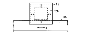
図14に示す第2変形例は、補助電極26の1辺(ループ状電極20の第1領域X)をアンテナパターン35の直線部分に重なるように搭載したものである。この場合、給電回路基板15がアンテナパターン35の線路長方向(矢印a参照)に位置ずれを生じても周波数特性は変動することがない。なお、ループ状電極20(コイルパターン21a~21d)がアンテナパターン35の線路長方向とは直交する部分であってアンテナパターン35と重なる部分の面積は、少ないほうが好ましい。
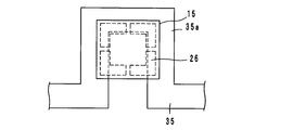
図15に示す第3変形例は、アンテナパターン35に屈曲部35aを形成し、該屈曲部35aに補助電極26(ループ状電極20)の3辺を重ね合わせたものである。補助電極26及びループ状電極20のそれぞれとアンテナパターン35との重なり領域が増加することにより、結合度が高くなる。
図16に示す第4変形例は、給電回路基板15を図6(B),(C)と同様にアンテナパターン35の内側コーナー部に配置したものであるが、補助電極26には一つのスリット26aのみが形成されている。このスリット26aはアンテナパターン35とは重ならないように配置される。
(第7実施例、図17参照)
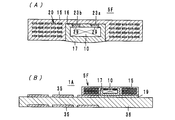
第7実施例である無線通信モジュール5Fは、図17(A)に示すように、給電回路基板15にキャビティ部16を基板15の裏面側に開口するように形成し、該キャビティ部16に無線ICチップ10を収容して封止材17を充填したものである。他の構成は前記第1実施例と同様である。この無線通信モジュール5Fは、図17(B)に示すように、キャビティ部16の開口部分がベース基材36に対向した状態でベース基材36上に絶縁性の接着剤19にて貼着され、無線通信デバイス1Aとされる。
第7実施例である無線通信モジュール5Fは、図17(A)に示すように、給電回路基板15にキャビティ部16を基板15の裏面側に開口するように形成し、該キャビティ部16に無線ICチップ10を収容して封止材17を充填したものである。他の構成は前記第1実施例と同様である。この無線通信モジュール5Fは、図17(B)に示すように、キャビティ部16の開口部分がベース基材36に対向した状態でベース基材36上に絶縁性の接着剤19にて貼着され、無線通信デバイス1Aとされる。
この無線通信モジュール5F及び無線通信デバイス1Aの作用効果は、基本的には図2に示したものと同様であり、特にキャビティ部16の底面(図17(A)では上面に配置されている)によって無線ICチップ10が保護される。また、給電回路基板15の底面(図10(A)では上面となっている)は平坦性が高いので、無線通信モジュール5Fをベース基材36上にマウンタで真空吸引して搭載する場合の吸引性能が良好である。さらに、図17(A)に示すように、封止材17がキャビティ部16から若干突出した状態となるので、ベース基材36への搭載時(接着剤19での接着時)に突出部分がアンカー効果を発揮し、給電回路基板15がベース基材36上に強固に接合されることになる。なお、封止材17がこれとは逆に凹状となっていても、アンカー効果が発揮される。
(無線通信デバイスの第3例、図18~図20参照)
次に、無線通信モジュール5を搭載した無線通信デバイスの第3例について説明する。
次に、無線通信モジュール5を搭載した無線通信デバイスの第3例について説明する。
図18に示すように、無線通信デバイス1Bは、無線通信モジュール5を円形状をなすフレキシブルなベース基材36A上に搭載したもので、ベース基材36Aの表裏面には図19(A),(B)に示す第2例としてのアンテナパターン35Aが形成されている。なお、図19(B)に示す裏面側のアンテナパターン35Aは表面側から透視した状態で示している。アンテナパターン35Aは、円形状に巻回され、ほぼ全長にわたって互いに平面視で重なっており、互いに容量結合している。アンテナパターン35Aは、図20に示す等価回路を形成しており、表面側のアンテナパターン35AによるインダクタL1と裏面側のアンテナパターン35AによるインダクタL2とが、最内パターンどうしの容量C1と最外パターンどうしの容量C2によって結合され、かつ、表裏のパターン間にも容量C3が発生している。
互いに容量結合しているアンテナパターン35Aの作用は図2に示したアンテナパターン35と同様であり、電流は同じ方向に流れる。そして、ベース基材36Aの表面であってアンテナパターン35Aと部分的に重なるように配置された無線通信モジュール5のコイル状電極20とアンテナパターン35Aとが磁界結合している。それゆえ、リーダライタのアンテナと無線通信モジュール5とがアンテナパターン35Aを介して通信が可能となる。無線通信デバイス1Bの基本的な作用効果は前記無線通信デバイス1で説明したとおりである。
なお、本無線通信デバイス1Bにおいて、ベース基材36Aの表裏に配置されたアンテナパターン35Aの両端部をそれぞれクリンピング(パウチング)によって直流的に結合させてもよく、一方端部どうしを同様に直流的に結合させてもよい。要は、表裏のアンテナパターン35Aに流れる電流の向きが同じ方向となるように結合していればよい。
(アンテナパターンの第3例、図21参照)
図21に第3例であるアンテナパターン35Bを示す。このアンテナパターン35Bは方形部35B'を有する概略円形状をなし、ベース基材36Aの表裏面に形成され、裏面側のアンテナパターンは表面側のアンテナパターン35Bと平面視で重なるように形成されている。表裏面のアンテナパターン35Bは互いに容量結合しており、その等価回路は図20と同様である。
図21に第3例であるアンテナパターン35Bを示す。このアンテナパターン35Bは方形部35B'を有する概略円形状をなし、ベース基材36Aの表裏面に形成され、裏面側のアンテナパターンは表面側のアンテナパターン35Bと平面視で重なるように形成されている。表裏面のアンテナパターン35Bは互いに容量結合しており、その等価回路は図20と同様である。
無線通信モジュール5は、ベース基材36Aの表面側であって、方形部35B'の内周部分に沿って搭載され、無線通信モジュール5に内蔵されているコイル状電極20がアンテナパターン35Bと磁界結合し、無線通信デバイスを構成する。アンテナパターン35Bの作用効果は前記アンテナパターン35Aで説明したとおりである。特に、アンテナパターン35Bは、コイル状電極20と3辺で結合しており、アンテナパターン35Bとコ
イル状電極20との結合量が多くなる。
イル状電極20との結合量が多くなる。
(アンテナパターンの第4例、図22参照)
図22に第4例であるアンテナパターン35Cを示す。このアンテナパターン35Cは階段状部35C'を有する概略円形状をなし、ベース基材36Aの表裏面に形成され、裏面側のアンテナパターンは表面側のアンテナパターン35Cと平面視で重なるように形成されている。表裏面のアンテナパターン35Cは互いに容量結合しており、その等価回路は図20と同様である。
図22に第4例であるアンテナパターン35Cを示す。このアンテナパターン35Cは階段状部35C'を有する概略円形状をなし、ベース基材36Aの表裏面に形成され、裏面側のアンテナパターンは表面側のアンテナパターン35Cと平面視で重なるように形成されている。表裏面のアンテナパターン35Cは互いに容量結合しており、その等価回路は図20と同様である。
無線通信モジュール5は、ベース基材36Aの表面側であって、階段状部35C'の内周部分に沿って搭載され、コイル状電極20がアンテナパターン35Cと磁界結合し、無線通信デバイスを構成する。アンテナパターン35Cの作用効果は前記アンテナパターン35Aで説明したとおりである。特に、アンテナパターン35Cは、コイル状電極20と2辺で結合しており、アンテナパターン35Cとコイル状電極20との結合量が多くなる。
(アンテナパターンの第5例、図23参照)
図23に第5例であるアンテナパターン35Dを示す。このアンテナパターン35Dは、図19に示したアンテナパターン35Aと基本的には同じ形状に配置され、最外ターン部分35D’が他の部分よりも線太に形成されている。他の構成及び作用効果は基本的には前記アンテナパターン35Aで説明したとおりである。加えて、最外ターン部分35D’での結合容量値が大きくなるため、アンテナパターン35Dの共振周波数を低下させることができる。換言すれば、アンテナパターン35Dでは開口径を小さくしないで磁束の通過領域を大きくできる。つまり、アンテナパターン35Dでは全体のサイズを大きくすることなく、共振周波数の低域側へのシフト、及び、通信距離の維持、向上を実現できる。
図23に第5例であるアンテナパターン35Dを示す。このアンテナパターン35Dは、図19に示したアンテナパターン35Aと基本的には同じ形状に配置され、最外ターン部分35D’が他の部分よりも線太に形成されている。他の構成及び作用効果は基本的には前記アンテナパターン35Aで説明したとおりである。加えて、最外ターン部分35D’での結合容量値が大きくなるため、アンテナパターン35Dの共振周波数を低下させることができる。換言すれば、アンテナパターン35Dでは開口径を小さくしないで磁束の通過領域を大きくできる。つまり、アンテナパターン35Dでは全体のサイズを大きくすることなく、共振周波数の低域側へのシフト、及び、通信距離の維持、向上を実現できる。
(アンテナパターンの第6例、図24及び図25参照)
図24に第6例であるアンテナパターン35Eを示す。このアンテナパターン35Eは、図23に示したアンテナパターン35Dと同様に最外ターン部分35E'を線太とし、ベース基材36Aの表裏面に配置したアンテナパターン35Eの一端35E”どうしをクリンピング(パウチング)によって直流的に結合したものである。アンテナパターン35Eは図25に示す等価回路を形成し、表面側のアンテナパターン35EによるインダクタL1と裏面側のアンテナパターン35EによるインダクタL2とが互いに磁気結合Mし、かつ、一端35E”で直流的に結合し、最外ターン部分35E”どうしは容量C2によって結合されている。
図24に第6例であるアンテナパターン35Eを示す。このアンテナパターン35Eは、図23に示したアンテナパターン35Dと同様に最外ターン部分35E'を線太とし、ベース基材36Aの表裏面に配置したアンテナパターン35Eの一端35E”どうしをクリンピング(パウチング)によって直流的に結合したものである。アンテナパターン35Eは図25に示す等価回路を形成し、表面側のアンテナパターン35EによるインダクタL1と裏面側のアンテナパターン35EによるインダクタL2とが互いに磁気結合Mし、かつ、一端35E”で直流的に結合し、最外ターン部分35E”どうしは容量C2によって結合されている。
互いに磁気結合しているアンテナパターン35Eの作用は図19に示したアンテナパターン35Aと同様である。特に、アンテナパターン35Eでは、前記アンテナパターン35Dと同様に、最外ターン部分35E’での結合容量値が大きくなるため、アンテナパターン35Eの共振周波数を低下させることができる。換言すれば、アンテナパターン35Eでは開口径を小さくしないで磁束の通過領域を大きくできる。つまり、アンテナパターン35Eでは全体のサイズを大きくすることなく、共振周波数の低域側へのシフト、及び、通信距離の維持、向上を実現できる。
(ICカード、図26参照)
本発明に係る無線通信端末の一例として、図26にICカード50を示す。このICカード50は前記無線通信デバイス1を内蔵させたものである。
本発明に係る無線通信端末の一例として、図26にICカード50を示す。このICカード50は前記無線通信デバイス1を内蔵させたものである。
(他の実施例)
なお、本発明に係る無線通信モジュール、無線通信デバイス及び無線通信端末は前記実施例に限定するものではなく、その要旨の範囲内で種々に変更することができる。
なお、本発明に係る無線通信モジュール、無線通信デバイス及び無線通信端末は前記実施例に限定するものではなく、その要旨の範囲内で種々に変更することができる。
例えば、前記実施例において、補助電極は、ループ状電極の略全域と重なるように配置したが、補助電極は、ループ状電極とアンテナパターンとが重なる位置に配置されていればよい。また、前記実施例において、ループ状電極は、コイルパターンを複数ターン巻回させて所定幅としたが、1ターン巻回させて所定幅としてもよい。また、コイルパターンを多層に巻回せず、単層に巻回してもよい。
また、無線ICはチップ状として給電回路基板上に搭載されるもの以外に、給電回路基板の内部に一体的に形成されていてもよい。また、無線ICはチップとして給電回路基板の近傍に配置される他の基板に搭載されていてもよい。また、無線通信デバイスは前記ICカード以外に種々の携帯用品に搭載することができる。
また、無線ICチップとループ状電極とはDC接続(直結)していなくてもよく、電磁界を介して結合していてもよい。即ち、電気的に接続していればよい。
また、アンテナパターンはアンテナとしての役割を果たすものであれば、種々の形状であってもよい。また、13.56MHz帯のようなHF帯に限定されず、UHF帯やSHF帯の無線通信デバイスにも利用できる。
以上のように、本発明は、無線通信モジュール、無線通信デバイスや無線通信端末に有用であり、特に、アンテナパターンに対する給電回路基板の位置精度が緩和され、生産効率が高まる点で優れている。
1,1A,1B…無線通信デバイス
5,5A~5F…無線通信モジュール
10…無線ICチップ
15…給電回路基板
20…ループ状電極
21a~21d…コイルパターン
26…補助電極
26a…スリット
35,35A~35E…アンテナパターン
5,5A~5F…無線通信モジュール
10…無線ICチップ
15…給電回路基板
20…ループ状電極
21a~21d…コイルパターン
26…補助電極
26a…スリット
35,35A~35E…アンテナパターン
Claims (10)
- 無線信号を処理する無線ICと、
前記無線ICに結合されたループ状電極及び補助電極を含む給電回路基板と、
を備え、
前記ループ状電極はコイルパターンを巻回してなり、
前記補助電極は、コイル軸方向から平面視したとき、前記ループ状電極の少なくとも一部と重なるように配置され、少なくとも一部に該補助電極を複数に分割するスリットが形成されていること、
を特徴とする無線通信モジュール。 - 前記補助電極は四角形のループ状をなし、4辺のそれぞれに前記スリットが形成されていること、を特徴とする請求項1に記載の無線通信モジュール。
- 前記コイルパターンは同一平面にて複数ターン巻回されていること、を特徴とする請求項1又は請求項2に記載の無線通信モジュール。
- 前記給電回路基板は多層基板からなり、前記コイルパターンは層間導体を介して多層に巻回されていること、を特徴とする請求項1ないし請求項3のいずれかに記載の無線通信モジュール。
- 無線信号を処理する無線ICと、
前記無線ICに結合されたループ状電極及び補助電極を含む給電回路基板と、
前記ループ状電極及び前記補助電極と結合されたアンテナパターンと、
を備え、
前記ループ状電極はコイルパターンを巻回してなり、
前記補助電極は、コイル軸方向から平面視したとき、前記ループ状電極の少なくとも一部と重なるように配置され、少なくとも一部に該補助電極を複数に分割するスリットが形成されており、
前記ループ状電極は、コイル軸方向から平面視したとき、少なくとも一部が前記アンテナパターンと重なるように配置されており、
前記補助電極は、コイル軸方向から平面視したとき、少なくとも一部が前記ループ状電極及び前記アンテナパターンと重なるように配置され、かつ、少なくとも一つの前記スリットが前記アンテナパターンとは重ならないように配置されていること、
を特徴とする無線通信デバイス。 - 前記補助電極は前記ループ状電極と前記アンテナパターンとの間に配置されていること、を特徴とする請求項5に記載の無線通信デバイス。
- 前記補助電極は四角形のループ状をなし、4辺のそれぞれに前記スリットが形成されていること、を特徴とする請求項5又は請求項6に記載の無線通信デバイス。
- 前記コイルパターンは同一平面にて複数ターン巻回されていること、を特徴とする請求項5ないし請求項7のいずれかに記載の無線通信デバイス。
- 前記給電回路基板は多層基板からなり、前記コイルパターンは層間導体を介して多層に巻回されていること、を特徴とする請求項5ないし請求項8のいずれかに記載の無線通信デバイス。
- 無線通信デバイスを備えた無線通信端末であって、
前記無線通信デバイスは、
無線信号を処理する無線ICと、
前記無線ICに結合されたループ状電極及び補助電極を含む給電回路基板と、
前記ループ状電極及び前記補助電極と結合されたアンテナパターンと、
を備え、
前記ループ状電極はコイルパターンを巻回してなり、
前記補助電極は、コイル軸方向から平面視したとき、前記ループ状電極の少なくとも一部と重なるように配置され、少なくとも一部に該補助電極を複数に分割するスリットが形成されており、
前記ループ状電極は、コイル軸方向から平面視したとき、少なくとも一部が前記ループ状電極及び前記アンテナパターンと重なるように配置されており、
前記補助電極は、コイル軸方向から平面視したとき、少なくとも一部が前記アンテナパターンと重なるように配置され、かつ、少なくとも一つの前記スリットが前記アンテナパターンとは重ならないように配置されていること、
を特徴とする無線通信端末。
Priority Applications (1)
| Application Number | Priority Date | Filing Date | Title |
|---|---|---|---|
| JP2012503047A JP5403145B2 (ja) | 2010-03-03 | 2011-02-08 | 無線通信デバイス及び無線通信端末 |
Applications Claiming Priority (2)
| Application Number | Priority Date | Filing Date | Title |
|---|---|---|---|
| JP2010046524 | 2010-03-03 | ||
| JP2010-046524 | 2010-03-03 |
Publications (1)
| Publication Number | Publication Date |
|---|---|
| WO2011108339A1 true WO2011108339A1 (ja) | 2011-09-09 |
Family
ID=44542005
Family Applications (1)
| Application Number | Title | Priority Date | Filing Date |
|---|---|---|---|
| PCT/JP2011/052593 Ceased WO2011108339A1 (ja) | 2010-03-03 | 2011-02-08 | 無線通信モジュール、無線通信デバイス及び無線通信端末 |
Country Status (2)
| Country | Link |
|---|---|
| JP (2) | JP5403145B2 (ja) |
| WO (1) | WO2011108339A1 (ja) |
Cited By (6)
| Publication number | Priority date | Publication date | Assignee | Title |
|---|---|---|---|---|
| WO2015115402A1 (ja) * | 2014-01-30 | 2015-08-06 | 株式会社村田製作所 | 無線通信装置 |
| JP5790907B1 (ja) * | 2014-03-17 | 2015-10-07 | 株式会社村田製作所 | アンテナ装置、無線通信端末 |
| WO2016194495A1 (ja) * | 2015-06-02 | 2016-12-08 | 凸版印刷株式会社 | 非接触型情報媒体 |
| JP2016224815A (ja) * | 2015-06-02 | 2016-12-28 | 凸版印刷株式会社 | 非接触型情報媒体 |
| JP2017010154A (ja) * | 2015-06-18 | 2017-01-12 | 凸版印刷株式会社 | 非接触型情報媒体 |
| WO2017169709A1 (ja) * | 2016-03-31 | 2017-10-05 | 株式会社村田製作所 | コイルアンテナ、給電装置、受電装置およびワイヤレス電力供給システム |
Families Citing this family (1)
| Publication number | Priority date | Publication date | Assignee | Title |
|---|---|---|---|---|
| JP5652470B2 (ja) * | 2010-03-03 | 2015-01-14 | 株式会社村田製作所 | 無線通信モジュール及び無線通信デバイス |
Citations (4)
| Publication number | Priority date | Publication date | Assignee | Title |
|---|---|---|---|---|
| JP2008217613A (ja) * | 2007-03-06 | 2008-09-18 | Dainippon Printing Co Ltd | 非接触型データキャリア装置 |
| JP2008226099A (ja) * | 2007-03-15 | 2008-09-25 | Dainippon Printing Co Ltd | 非接触式データキャリア装置 |
| WO2009011376A1 (ja) * | 2007-07-18 | 2009-01-22 | Murata Manufacturing Co., Ltd. | 無線icデバイス |
| JP2009027291A (ja) * | 2007-07-18 | 2009-02-05 | Murata Mfg Co Ltd | 無線icデバイス |
Family Cites Families (3)
| Publication number | Priority date | Publication date | Assignee | Title |
|---|---|---|---|---|
| JP2001094326A (ja) * | 1999-09-22 | 2001-04-06 | Matsushita Electric Ind Co Ltd | カードリーダ用アンテナ |
| JP2001326526A (ja) * | 2000-05-16 | 2001-11-22 | Mitsubishi Electric Corp | シールドアンテナコイル |
| JP2008288845A (ja) * | 2007-05-17 | 2008-11-27 | Nippon Telegr & Teleph Corp <Ntt> | 読み書き装置 |
-
2011
- 2011-02-08 WO PCT/JP2011/052593 patent/WO2011108339A1/ja not_active Ceased
- 2011-02-08 JP JP2012503047A patent/JP5403145B2/ja not_active Expired - Fee Related
-
2013
- 2013-10-30 JP JP2013225433A patent/JP5660188B2/ja not_active Expired - Fee Related
Patent Citations (4)
| Publication number | Priority date | Publication date | Assignee | Title |
|---|---|---|---|---|
| JP2008217613A (ja) * | 2007-03-06 | 2008-09-18 | Dainippon Printing Co Ltd | 非接触型データキャリア装置 |
| JP2008226099A (ja) * | 2007-03-15 | 2008-09-25 | Dainippon Printing Co Ltd | 非接触式データキャリア装置 |
| WO2009011376A1 (ja) * | 2007-07-18 | 2009-01-22 | Murata Manufacturing Co., Ltd. | 無線icデバイス |
| JP2009027291A (ja) * | 2007-07-18 | 2009-02-05 | Murata Mfg Co Ltd | 無線icデバイス |
Cited By (10)
| Publication number | Priority date | Publication date | Assignee | Title |
|---|---|---|---|---|
| WO2015115402A1 (ja) * | 2014-01-30 | 2015-08-06 | 株式会社村田製作所 | 無線通信装置 |
| JP5790904B1 (ja) * | 2014-01-30 | 2015-10-07 | 株式会社村田製作所 | 無線通信装置 |
| US9947991B2 (en) | 2014-01-30 | 2018-04-17 | Murata Manufacturing Co., Ltd. | Radio communication device |
| JP5790907B1 (ja) * | 2014-03-17 | 2015-10-07 | 株式会社村田製作所 | アンテナ装置、無線通信端末 |
| WO2016194495A1 (ja) * | 2015-06-02 | 2016-12-08 | 凸版印刷株式会社 | 非接触型情報媒体 |
| JP2016224815A (ja) * | 2015-06-02 | 2016-12-28 | 凸版印刷株式会社 | 非接触型情報媒体 |
| US10217040B2 (en) | 2015-06-02 | 2019-02-26 | Toppan Printing Co., Ltd. | Contactless information medium |
| JP2017010154A (ja) * | 2015-06-18 | 2017-01-12 | 凸版印刷株式会社 | 非接触型情報媒体 |
| WO2017169709A1 (ja) * | 2016-03-31 | 2017-10-05 | 株式会社村田製作所 | コイルアンテナ、給電装置、受電装置およびワイヤレス電力供給システム |
| JPWO2017169709A1 (ja) * | 2016-03-31 | 2018-11-29 | 株式会社村田製作所 | コイルアンテナ、給電装置、受電装置およびワイヤレス電力供給システム |
Also Published As
| Publication number | Publication date |
|---|---|
| JP5660188B2 (ja) | 2015-01-28 |
| JPWO2011108339A1 (ja) | 2013-06-24 |
| JP5403145B2 (ja) | 2014-01-29 |
| JP2014017884A (ja) | 2014-01-30 |
Similar Documents
| Publication | Publication Date | Title |
|---|---|---|
| US8602310B2 (en) | Radio communication device and radio communication terminal | |
| CN102792520B (zh) | 无线通信模块以及无线通信设备 | |
| US11392784B2 (en) | RFID system | |
| JP5376060B2 (ja) | アンテナ及びrfidデバイス | |
| KR101006808B1 (ko) | 무선 ic 디바이스 | |
| US8366009B2 (en) | Coupling in and to RFID smart cards | |
| US9165240B2 (en) | Coupling in and to RFID smart cards | |
| JP5660188B2 (ja) | 無線通信モジュール | |
| JP6260729B2 (ja) | 給電素子 | |
| US20160156104A1 (en) | Antenna device and communication terminal apparatus | |
| WO2012093541A1 (ja) | 無線通信デバイス | |
| JP2012059015A (ja) | 無線icタグ及びrfidシステム | |
| JP2013141164A (ja) | アンテナ装置および通信端末装置 | |
| US10522911B2 (en) | Antenna device, card-type information medium, and communication terminal apparatus | |
| JP5655602B2 (ja) | アンテナおよびrfidデバイス | |
| JP5637004B2 (ja) | 半導体集積回路モジュール、無線通信モジュール及び無線通信デバイス | |
| JP5983724B2 (ja) | 無線icタグ及びrfidシステム |
Legal Events
| Date | Code | Title | Description |
|---|---|---|---|
| 121 | Ep: the epo has been informed by wipo that ep was designated in this application |
Ref document number: 11750452 Country of ref document: EP Kind code of ref document: A1 |
|
| WWE | Wipo information: entry into national phase |
Ref document number: 2012503047 Country of ref document: JP |
|
| NENP | Non-entry into the national phase |
Ref country code: DE |
|
| 122 | Ep: pct application non-entry in european phase |
Ref document number: 11750452 Country of ref document: EP Kind code of ref document: A1 |