WO2011105514A1 - Liquid crystal display device - Google Patents
Liquid crystal display device Download PDFInfo
- Publication number
- WO2011105514A1 WO2011105514A1 PCT/JP2011/054185 JP2011054185W WO2011105514A1 WO 2011105514 A1 WO2011105514 A1 WO 2011105514A1 JP 2011054185 W JP2011054185 W JP 2011054185W WO 2011105514 A1 WO2011105514 A1 WO 2011105514A1
- Authority
- WO
- WIPO (PCT)
- Prior art keywords
- pixel
- subpixel
- liquid crystal
- pixels
- voltage
- Prior art date
Links
Images


Classifications
-
- G—PHYSICS
- G09—EDUCATION; CRYPTOGRAPHY; DISPLAY; ADVERTISING; SEALS
- G09G—ARRANGEMENTS OR CIRCUITS FOR CONTROL OF INDICATING DEVICES USING STATIC MEANS TO PRESENT VARIABLE INFORMATION
- G09G3/00—Control arrangements or circuits, of interest only in connection with visual indicators other than cathode-ray tubes
- G09G3/20—Control arrangements or circuits, of interest only in connection with visual indicators other than cathode-ray tubes for presentation of an assembly of a number of characters, e.g. a page, by composing the assembly by combination of individual elements arranged in a matrix no fixed position being assigned to or needed to be assigned to the individual characters or partial characters
- G09G3/34—Control arrangements or circuits, of interest only in connection with visual indicators other than cathode-ray tubes for presentation of an assembly of a number of characters, e.g. a page, by composing the assembly by combination of individual elements arranged in a matrix no fixed position being assigned to or needed to be assigned to the individual characters or partial characters by control of light from an independent source
- G09G3/36—Control arrangements or circuits, of interest only in connection with visual indicators other than cathode-ray tubes for presentation of an assembly of a number of characters, e.g. a page, by composing the assembly by combination of individual elements arranged in a matrix no fixed position being assigned to or needed to be assigned to the individual characters or partial characters by control of light from an independent source using liquid crystals
- G09G3/3607—Control arrangements or circuits, of interest only in connection with visual indicators other than cathode-ray tubes for presentation of an assembly of a number of characters, e.g. a page, by composing the assembly by combination of individual elements arranged in a matrix no fixed position being assigned to or needed to be assigned to the individual characters or partial characters by control of light from an independent source using liquid crystals for displaying colours or for displaying grey scales with a specific pixel layout, e.g. using sub-pixels
-
- G—PHYSICS
- G09—EDUCATION; CRYPTOGRAPHY; DISPLAY; ADVERTISING; SEALS
- G09G—ARRANGEMENTS OR CIRCUITS FOR CONTROL OF INDICATING DEVICES USING STATIC MEANS TO PRESENT VARIABLE INFORMATION
- G09G3/00—Control arrangements or circuits, of interest only in connection with visual indicators other than cathode-ray tubes
- G09G3/20—Control arrangements or circuits, of interest only in connection with visual indicators other than cathode-ray tubes for presentation of an assembly of a number of characters, e.g. a page, by composing the assembly by combination of individual elements arranged in a matrix no fixed position being assigned to or needed to be assigned to the individual characters or partial characters
- G09G3/34—Control arrangements or circuits, of interest only in connection with visual indicators other than cathode-ray tubes for presentation of an assembly of a number of characters, e.g. a page, by composing the assembly by combination of individual elements arranged in a matrix no fixed position being assigned to or needed to be assigned to the individual characters or partial characters by control of light from an independent source
- G09G3/36—Control arrangements or circuits, of interest only in connection with visual indicators other than cathode-ray tubes for presentation of an assembly of a number of characters, e.g. a page, by composing the assembly by combination of individual elements arranged in a matrix no fixed position being assigned to or needed to be assigned to the individual characters or partial characters by control of light from an independent source using liquid crystals
- G09G3/3611—Control of matrices with row and column drivers
- G09G3/3648—Control of matrices with row and column drivers using an active matrix
- G09G3/3651—Control of matrices with row and column drivers using an active matrix using multistable liquid crystals, e.g. ferroelectric liquid crystals
-
- G—PHYSICS
- G02—OPTICS
- G02F—OPTICAL DEVICES OR ARRANGEMENTS FOR THE CONTROL OF LIGHT BY MODIFICATION OF THE OPTICAL PROPERTIES OF THE MEDIA OF THE ELEMENTS INVOLVED THEREIN; NON-LINEAR OPTICS; FREQUENCY-CHANGING OF LIGHT; OPTICAL LOGIC ELEMENTS; OPTICAL ANALOGUE/DIGITAL CONVERTERS
- G02F1/00—Devices or arrangements for the control of the intensity, colour, phase, polarisation or direction of light arriving from an independent light source, e.g. switching, gating or modulating; Non-linear optics
- G02F1/01—Devices or arrangements for the control of the intensity, colour, phase, polarisation or direction of light arriving from an independent light source, e.g. switching, gating or modulating; Non-linear optics for the control of the intensity, phase, polarisation or colour
- G02F1/13—Devices or arrangements for the control of the intensity, colour, phase, polarisation or direction of light arriving from an independent light source, e.g. switching, gating or modulating; Non-linear optics for the control of the intensity, phase, polarisation or colour based on liquid crystals, e.g. single liquid crystal display cells
- G02F1/133—Constructional arrangements; Operation of liquid crystal cells; Circuit arrangements
- G02F1/1333—Constructional arrangements; Manufacturing methods
- G02F1/1343—Electrodes
- G02F1/134309—Electrodes characterised by their geometrical arrangement
- G02F1/134345—Subdivided pixels, e.g. for grey scale or redundancy
-
- G—PHYSICS
- G02—OPTICS
- G02F—OPTICAL DEVICES OR ARRANGEMENTS FOR THE CONTROL OF LIGHT BY MODIFICATION OF THE OPTICAL PROPERTIES OF THE MEDIA OF THE ELEMENTS INVOLVED THEREIN; NON-LINEAR OPTICS; FREQUENCY-CHANGING OF LIGHT; OPTICAL LOGIC ELEMENTS; OPTICAL ANALOGUE/DIGITAL CONVERTERS
- G02F1/00—Devices or arrangements for the control of the intensity, colour, phase, polarisation or direction of light arriving from an independent light source, e.g. switching, gating or modulating; Non-linear optics
- G02F1/01—Devices or arrangements for the control of the intensity, colour, phase, polarisation or direction of light arriving from an independent light source, e.g. switching, gating or modulating; Non-linear optics for the control of the intensity, phase, polarisation or colour
- G02F1/13—Devices or arrangements for the control of the intensity, colour, phase, polarisation or direction of light arriving from an independent light source, e.g. switching, gating or modulating; Non-linear optics for the control of the intensity, phase, polarisation or colour based on liquid crystals, e.g. single liquid crystal display cells
- G02F1/133—Constructional arrangements; Operation of liquid crystal cells; Circuit arrangements
- G02F1/136—Liquid crystal cells structurally associated with a semi-conducting layer or substrate, e.g. cells forming part of an integrated circuit
- G02F1/1362—Active matrix addressed cells
- G02F1/13624—Active matrix addressed cells having more than one switching element per pixel
-
- G—PHYSICS
- G09—EDUCATION; CRYPTOGRAPHY; DISPLAY; ADVERTISING; SEALS
- G09G—ARRANGEMENTS OR CIRCUITS FOR CONTROL OF INDICATING DEVICES USING STATIC MEANS TO PRESENT VARIABLE INFORMATION
- G09G2300/00—Aspects of the constitution of display devices
- G09G2300/04—Structural and physical details of display devices
- G09G2300/0439—Pixel structures
- G09G2300/0443—Pixel structures with several sub-pixels for the same colour in a pixel, not specifically used to display gradations
-
- G—PHYSICS
- G09—EDUCATION; CRYPTOGRAPHY; DISPLAY; ADVERTISING; SEALS
- G09G—ARRANGEMENTS OR CIRCUITS FOR CONTROL OF INDICATING DEVICES USING STATIC MEANS TO PRESENT VARIABLE INFORMATION
- G09G2300/00—Aspects of the constitution of display devices
- G09G2300/04—Structural and physical details of display devices
- G09G2300/0439—Pixel structures
- G09G2300/0452—Details of colour pixel setup, e.g. pixel composed of a red, a blue and two green components
-
- G—PHYSICS
- G09—EDUCATION; CRYPTOGRAPHY; DISPLAY; ADVERTISING; SEALS
- G09G—ARRANGEMENTS OR CIRCUITS FOR CONTROL OF INDICATING DEVICES USING STATIC MEANS TO PRESENT VARIABLE INFORMATION
- G09G2310/00—Command of the display device
- G09G2310/06—Details of flat display driving waveforms
-
- G—PHYSICS
- G09—EDUCATION; CRYPTOGRAPHY; DISPLAY; ADVERTISING; SEALS
- G09G—ARRANGEMENTS OR CIRCUITS FOR CONTROL OF INDICATING DEVICES USING STATIC MEANS TO PRESENT VARIABLE INFORMATION
- G09G2320/00—Control of display operating conditions
- G09G2320/02—Improving the quality of display appearance
- G09G2320/028—Improving the quality of display appearance by changing the viewing angle properties, e.g. widening the viewing angle, adapting the viewing angle to the view direction
-
- G—PHYSICS
- G09—EDUCATION; CRYPTOGRAPHY; DISPLAY; ADVERTISING; SEALS
- G09G—ARRANGEMENTS OR CIRCUITS FOR CONTROL OF INDICATING DEVICES USING STATIC MEANS TO PRESENT VARIABLE INFORMATION
- G09G3/00—Control arrangements or circuits, of interest only in connection with visual indicators other than cathode-ray tubes
- G09G3/20—Control arrangements or circuits, of interest only in connection with visual indicators other than cathode-ray tubes for presentation of an assembly of a number of characters, e.g. a page, by composing the assembly by combination of individual elements arranged in a matrix no fixed position being assigned to or needed to be assigned to the individual characters or partial characters
- G09G3/34—Control arrangements or circuits, of interest only in connection with visual indicators other than cathode-ray tubes for presentation of an assembly of a number of characters, e.g. a page, by composing the assembly by combination of individual elements arranged in a matrix no fixed position being assigned to or needed to be assigned to the individual characters or partial characters by control of light from an independent source
- G09G3/36—Control arrangements or circuits, of interest only in connection with visual indicators other than cathode-ray tubes for presentation of an assembly of a number of characters, e.g. a page, by composing the assembly by combination of individual elements arranged in a matrix no fixed position being assigned to or needed to be assigned to the individual characters or partial characters by control of light from an independent source using liquid crystals
- G09G3/3611—Control of matrices with row and column drivers
- G09G3/3614—Control of polarity reversal in general
Definitions
- the present invention relates to a liquid crystal display device, and more particularly to a liquid crystal display device that has a pixel division structure and performs color display using four or more types of pixels that display different colors.
- An MVA (Multidomain Vertical Alignment) type liquid crystal display device has a wider viewing angle characteristic than a TN type liquid crystal display device, and is therefore widely used in liquid crystal display devices for TV applications (see, for example, Patent Documents 1 and 2). ).
- a director-alignment direction (tilt direction) is provided by providing a domain-regulating structure (also referred to as an alignment-regulating structure) on the liquid crystal layer side of a pair of substrates facing each other with a vertical alignment-type liquid crystal layer interposed therebetween. Form a plurality of liquid crystal domains.
- a domain-regulating structure also referred to as an alignment-regulating structure
- an opening (slit) provided in the electrode or a dielectric protrusion (rib) formed on the liquid crystal layer side of the electrode is used.
- a linear domain regulation structure extending in two directions orthogonal to each other is disposed on each of a pair of substrates, and when viewed from a direction perpendicular to the substrate, the domain regulation structure formed on one substrate
- the domain restriction structures arranged on the other substrate are arranged in parallel and alternately.
- the azimuth angle of the director of the liquid crystal domain forms 45 ° with respect to the polarization axes (transmission axes) of the pair of polarizing plates arranged in crossed Nicols.
- the azimuth angles of the directors of the four liquid crystal domains are 45 °, 135 °, 225 °, 315 °.
- the “pixel” in this specification refers to the minimum unit for display by the liquid crystal display device, and in the case of a color display device, it refers to the minimum unit for displaying individual primary colors, and is sometimes referred to as “dot”.
- one color display pixel is constituted by three pixels that display the three primary colors of light, red, green, and blue, and color display is performed by controlling the luminance of each pixel. ing.
- Patent Document 3 A liquid crystal display device and a driving method capable of improving the viewing angle dependency are disclosed.
- the normally black mode display it is possible to improve the viewing angle dependency of the ⁇ characteristic that the display luminance of the low gradation is higher than the predetermined luminance (becomes whitish).
- display or driving may be referred to as area gradation display, area gradation driving, multi-pixel display, or multi-pixel driving.
- color reproduction range For example, in addition to a red (R) pixel, a green (G) pixel, and a blue (B) pixel, at least one other color pixel (yellow (Y) pixel, cyan (C) pixel, magenta (M) pixel, or A liquid crystal display device including a color display pixel composed of white (W) pixels is disclosed. When white pixels are added, the display luminance can be increased although the color reproduction range cannot be widened.
- Patent Documents 1 to 3 The entire disclosure of Patent Documents 1 to 3 is incorporated herein by reference.
- the multi-pixel driving method described in Patent Document 3 supplies two auxiliary capacitors provided corresponding to two sub-pixels that are electrically independent from each other.
- the effective voltage applied to the liquid crystal layers of the two sub-pixels is made different from each other by making the storage capacitor counter voltage (also referred to as “CS signal voltage”) different.
- each auxiliary capacitor counter voltage is The effective amount applied to the liquid crystal layer of the two sub-pixels by changing the amount of change in the auxiliary capacitor counter voltage (including the change direction and the sign of the change amount) from each other for the two sub-pixels. Different voltages from each other.
- an effective voltage applied to the liquid crystal layer of any of the two sub-pixels by a combination of the polarity of the display signal voltage and the direction of change of the auxiliary capacitor counter voltage Is determined to be larger. Therefore, in a liquid crystal display device having a pixel division structure in which bright subpixels and dark subpixels are arranged in the column direction, for example, when one-dot inversion driving is performed in order to prevent flicker, the pixel is applied to the liquid crystal layer of the pixels.
- the bright sub-pixels are arranged in a zigzag manner along the row direction according to the polarity arrangement of the display signal voltage.
- the pixel arrangement in two color display pixels adjacent to each other in the row direction is, for example, R (+), G ( ⁇ ), B ( +), R ( ⁇ ), G (+), and B ( ⁇ ).
- the position of the bright subpixel in the column direction is, for example, R (upper), G (lower), and B (upper). ), R (lower), G (upper), and B (lower).
- the bright subpixels of R, B, and G are arranged on the upper side of the two pixels, and the bright subpixels of G, R, and B are arranged on the lower side, and three primary colors are arranged in each row constituted by the subpixels. There will be a bright sub-pixel.
- the arrangement of pixels in two color display pixels adjacent to each other in the row direction is, for example, as shown in FIG. (+), R (-), G (+), B (-), Y (+), R (-), G (+), B (-).
- the positions in the column direction are, for example, Y (upper), R (lower), G (upper), B (lower), Y (upper), R (lower), G (upper), and B (lower). Then, two Y and G bright subpixels are arranged on the upper side of the two pixels, and two R and B bright subpixels are arranged on the lower side.
- This problem is not limited to the case of four primary colors, but is a problem common to liquid crystal display devices with a stripe arrangement having an even number of primary color pixels in the row direction.
- the present invention has been made to solve the above-described problem, and the object thereof is configured by four or more even-numbered primary color pixels that do not cause a problem of color blur even when multi-pixel driving is performed.
- An object of the present invention is to provide a liquid crystal display device having color display pixels.
- the liquid crystal display device of the present invention includes a plurality of pixels arranged in a matrix having rows and columns, and each of the plurality of pixels includes a first subpixel and a second subpixel arranged in a column direction.
- One of the first subpixel and the second subpixel is a bright subpixel that exhibits higher brightness than the other at least in a certain gradation, and the other has a plurality of pixels that are dark subpixels.
- the plurality of pixels constitute a plurality of color display pixels, and each of the plurality of color display pixels includes an even number including first, second, third, and fourth pixels arranged in a row direction. In a row of arbitrary pixels, the row of subpixels including the bright subpixel includes the respective bright subpixels of the first, second, third, and fourth pixels.
- the arrangement in the column direction of the bright sub-pixel and the dark sub-pixel in any two color display pixels adjacent to each other in a row of arbitrary pixels is opposite to each other.
- the liquid crystal display device includes a plurality of source bus lines, each of which has a plurality of source bus lines associated with a certain column of pixels, and a plurality of gate bus lines, each of which has a certain row.
- a plurality of first CS bus lines each of which includes a plurality of first CS bus lines associated with the first subpixel and a plurality of second CS bus lines, each of which has a pixel.
- a plurality of second CS bus lines associated with the first subpixel wherein the first subpixel includes a first subpixel electrode, a liquid crystal layer, A liquid crystal capacitor formed by a counter electrode facing the first subpixel electrode through the liquid crystal layer, a first auxiliary capacitor electrode electrically connected to the first subpixel electrode, an insulating layer, , Having a first auxiliary capacitance formed by a first auxiliary capacitance counter electrode opposed to the first auxiliary capacitance electrode via the insulating layer, wherein the second subpixel includes a second subpixel electrode, a liquid crystal A liquid crystal capacitor formed by a layer and a counter electrode facing the second subpixel electrode through the liquid crystal layer, and a second auxiliary capacitor electrode electrically connected to the second subpixel electrode; Each of the first subpixel and the second subpixel includes a second auxiliary capacitance formed by an insulating layer and a second auxiliary capacitance counter electrode facing the second auxiliary capacitance electrode via the insulating layer.
- the TFT corresponding to When the TFT corresponding to is in the ON state, After the display signal voltage is supplied from the corresponding source bus line to the first and second subpixel electrodes and the first and second auxiliary capacitor counter electrodes, respectively, the TFT is turned off.
- the voltage of the first and second auxiliary capacitor counter electrodes changes, and the amount of change defined by the direction and magnitude of the change differs between the first subpixel and the second subpixel, and any color display In the pixel, the polarities of the display signal voltages supplied to the pixels adjacent to each other are opposite to each other, and the first, second, The polarities of the display signal voltages supplied to the third and fourth pixels are opposite to each other.
- the arrangement in the column direction of the bright subpixel and the dark subpixel in any two color display pixels adjacent to each other is the same.
- the liquid crystal display device includes a plurality of source bus lines, each of which has a plurality of source bus lines associated with a certain column of pixels, and a plurality of gate bus lines, each of which has a certain row.
- a plurality of first CS bus lines each of which has a plurality of first CS bus lines associated with the first sub-pixel of a certain pixel, wherein the first sub-pixel is a first sub-pixel.
- the sub-pixel has a liquid crystal capacitance formed by a second sub-pixel electrode and a counter electrode facing the second sub-pixel electrode through the liquid crystal layer, and the sub-pixel through the corresponding first CS bus line
- the first CS signal voltage supplied to the first auxiliary capacitance counter electrode is an oscillating voltage having a cycle shorter than one vertical scanning period, and includes a first potential and a second potential defining a maximum amplitude, and the first potential.
- the gate signal voltage supplied to the gate bus line associated with a pixel in any row is switched from high to low, at least three potentials including a third potential between the first potential and the second potential are taken.
- the first CS Wherein the 1CS signal voltage supplied to Surain is the third potential.
- the third potential is an average value of the first potential and the second potential.
- the apparatus further includes a plurality of second CS bus lines, each of which is associated with the second subpixel of a certain pixel, and the second subpixel includes the second subpixel, A second auxiliary capacitance electrode electrically connected to the second subpixel electrode, an insulating layer, and a second auxiliary capacitance counter electrode opposed to the second auxiliary capacitance electrode through the insulating layer.
- the second CS signal voltage having two auxiliary capacitors and supplied to the second auxiliary capacitor counter electrode via the corresponding second CS bus line is constant during one vertical scanning period.
- the second CS signal voltage is equal to the counter voltage supplied to the counter voltage.
- the second subpixel does not have an auxiliary capacitor.
- the first, second, third and fourth pixels include one of a yellow pixel, a cyan pixel, a magenta pixel and a white pixel, and a red pixel, a blue pixel and a green pixel.
- a liquid crystal display device having a color display pixel composed of an even number of four or more primary color pixels that does not cause a problem of color blur even when multi-pixel driving is performed.
- FIG. 1 It is a schematic diagram which shows an example of the pixel structure of 100 A of liquid crystal display devices of embodiment by this invention.
- A is a figure which shows the electrical equivalent circuit corresponding to the pixel structure of 100 A of liquid crystal display devices
- (b) is the electricity corresponding to the pixel structure of liquid crystal display device 100B of other embodiment by this invention.
- It is a figure which shows a typical equivalent circuit.
- It is a figure which shows typically the display state when 100 A of liquid crystal display devices of 1st Embodiment drive 1 dot inversion.
- FIG. It is a figure which shows typically the display state when the liquid crystal display device of patent document 3 carries out 1 dot inversion drive.
- (A)-(j) is a figure which shows the waveform of the various voltages (signal) for obtaining the display state shown in FIG.
- FIG. 1 schematically shows an electrical configuration of a liquid crystal display device 100A according to an embodiment of the present invention.
- the liquid crystal display device 100A has a plurality of pixels arranged in a matrix having rows and columns, and FIG. 1 shows the structure of one of the pixels.
- the pixel 10 is divided into sub-pixels 10a and 10b, and the sub-pixels 10a and 10b are connected to TFTs 16a and 16b and auxiliary capacitors (CS) 22a and 22b, respectively.
- the gate electrodes of the TFTs 16 a and 16 b are connected to a gate bus line (scanning line) 12, and the source electrodes are connected to a common (identical) source bus line (signal line) 14.
- the auxiliary capacitors 22a and 22b are connected to a CS bus line (auxiliary capacitor line) 24a and a CS bus line 24b, respectively.
- the auxiliary capacitors 22a and 22b are provided between the auxiliary capacitor electrode electrically connected to the sub-pixel electrodes 18a and 18b and the auxiliary capacitor counter electrode electrically connected to the CS bus lines 24a and 24b, respectively.
- the insulating layer (not shown) is formed.
- the auxiliary capacitor counter electrodes of the auxiliary capacitors 22a and 22b are independent from each other, and have a structure in which different auxiliary capacitor counter voltages (CS signal voltages) can be supplied from the CS bus lines 24a and 24b, respectively.
- FIG. 2 (a) schematically shows an equivalent circuit for one pixel of the liquid crystal display device 100A.
- the liquid crystal capacitors of the sub-pixels 10a and 10b are represented as liquid crystal capacitors 13a and 13b, respectively.
- the liquid crystal capacitors 13a and 13b are formed by subpixel electrodes 18a and 18b, a liquid crystal layer, and a counter electrode 17 (common to the subpixels 10a and 10b), respectively.
- the liquid crystal capacitors 13a and 13b are referred to as electrical components, they may be referred to as liquid crystal capacitors Clca and Clcb, respectively.
- One electrode of the liquid crystal capacitor Clca and the auxiliary capacitor Ccsa of the subpixel 10a is connected to the drain electrode of the TFT 16a provided to drive the subpixel 10a, and the other electrode of the liquid crystal capacitor Clca is connected to the counter electrode.
- the other electrode of the auxiliary capacitor Ccsa is connected to the CS bus line 24a.
- One electrode of the liquid crystal capacitor Clcb and the auxiliary capacitor Ccsb of the subpixel 10b is connected to the drain electrode of the TFT 16b provided to drive the subpixel 10b, and the other electrode of the liquid crystal capacitor Clcb is connected to the counter electrode.
- the other electrode of the auxiliary capacitor Ccsb is connected to the CS bus line 24b.
- the gate electrodes of the TFTs 16 a and 16 b are both connected to the gate bus line 12, and the source electrodes are both connected to the source bus line 14.
- the TFT 16a and the TFT 16b may be supplied with a common gate signal voltage and a common display signal voltage (source signal voltage), and the gate bus line 12 and / or the source bus line 14 may not be common.
- Patent Document 3 also discloses the same pixel structure as the liquid crystal display device 100A.
- the polarity of the display signal voltage supplied to the color display pixel adjacent to the side is changed. The distribution is different from that of the liquid crystal display device described in Patent Document 3 (FIG. 3).
- the auxiliary capacitor counter voltage (CS signal voltage) supplied to the CS bus lines 24a and 24b is an oscillating voltage, as in the liquid crystal display device described in Patent Document 3.
- the oscillating voltage is a voltage whose oscillation cycle is shorter than one vertical scanning period.
- a liquid crystal layer of one sub-pixel (a bright sub-pixel, in the following, an example in which the sub-pixel 10a is a bright sub-pixel) is included in the corresponding source.
- a display signal voltage supplied from the bus line 14 and a storage capacitor counter voltage (first CS signal voltage), which is an oscillation voltage supplied from the CS bus line 24a, are applied in a superimposed manner, while the other subpixel (subpixel) is applied.
- the display signal voltage is applied to the liquid crystal layer 10b), and no oscillating voltage is applied. Only the display signal voltage is substantially applied to the liquid crystal layer of the other subpixel (subpixel 10b).
- the storage capacitor counter voltage (second CS signal voltage) Vcsb supplied to the sub-pixel 10b of the liquid crystal display device 100A of the second embodiment is not a vibration voltage but a DC voltage (see Vcsb in FIG. 4).
- DC voltage refers to DC, that is, a voltage with a constant potential in one vertical scanning period.
- the DC voltage supplied as Vcsb is preferably equal to the counter voltage supplied to the counter voltage. Note that the magnitude of the voltage applied to the liquid crystal layer is expressed with reference to the potential of the counter electrode.
- the liquid crystal display device it is not necessary to apply an oscillating voltage to the liquid crystal layer of the sub-pixel 10b. Therefore, unlike the liquid crystal display device 100B shown in FIG. A configuration in which the sub-pixel 10b serving as the sub-pixel does not have an auxiliary capacitor may be employed. Thus, by omitting the auxiliary capacitor, the aperture ratio of the pixel can be increased.
- the vertical scanning period of a liquid crystal display device of 2 ⁇ speed driving or 4 ⁇ speed driving, that is, a conventional liquid crystal display device is 1/60 seconds (vertical scanning frequency is 60 Hz), whereas the vertical scanning period is 1/120 seconds.
- the auxiliary capacitor can be omitted because the time for holding the voltage applied to the liquid crystal layer is short.
- the CS signal voltage Vcsa supplied from the CS bus line 24a to the auxiliary capacitance counter electrode of the sub-pixel 10a is one vertical scan as shown in FIG. It is an oscillating voltage having a cycle shorter than the period, and takes at least three potentials including a first potential and a second potential that define the maximum amplitude, and a third potential between the first potential and the second potential. As illustrated, the third potential is preferably an average value of the first potential and the second potential. The first, second and third potentials are preferably maintained for a certain time as shown.
- the liquid crystal display devices 100A and 100B according to the second embodiment of the present invention can solve the above-described problem of multi-pixel driving described in Patent Document 3 while improving the viewing angle dependency of the ⁇ characteristic. .
- the “vertical scanning period” means a period until a gate bus line (scanning line) is selected and then the gate bus line is selected.
- one vertical scanning period corresponds to one frame period of a video signal when the video signal is a signal for non-interlace driving, and when the video signal is a signal for interlace driving.
- one vertical scanning period of the liquid crystal display device is 16.7 msec which is the reciprocal of the field frequency (60 Hz) of the NTSC signal.
- the liquid crystal display device Since the liquid crystal display device does not perform interlaced driving, signal voltages are written to all pixels in both odd and even fields, so the reciprocal of the field frequency of the NTSC signal is the vertical scanning period.
- the difference (period) between the time for selecting a certain gate bus line and the time for selecting the next gate bus line is referred to as one horizontal scanning period (1H).
- the pixel structure of the liquid crystal display device 100A according to the embodiment of the present invention is the same as the pixel structure described in Patent Document 3, and the principle of making a bright subpixel by supplying an auxiliary capacitance voltage as an oscillation voltage is also common. Therefore, the principle of the multi-pixel driving method described in Patent Document 3 will also be described.
- a liquid crystal display device having the same structure as that shown in FIGS. 1 and 2A and driven using the voltages shown in FIGS. 7A to 7F will be described as an example.
- 7A to 7F schematically show the timing of each voltage when driving a liquid crystal display device having the same pixel structure as the liquid crystal display device 100A.
- 7A shows the voltage waveform Vs of the source bus line 14
- FIG. 7B shows the voltage waveform Vcsa of the CS bus line 24a
- FIG. 7C shows the voltage waveform Vcsb of the CS bus line 24b
- FIG. ) Shows the voltage waveform Vg of the gate bus line 12
- FIG. 7E shows the voltage waveform Vlca of the pixel electrode 18a of the subpixel 10a
- FIG. 7F shows the voltage waveform Vlcb of the pixel electrode 18b of the subpixel 10b.
- the broken line in the figure shows the voltage waveform COMMON (Vcom) of the counter electrode 17.
- the capacitance values of the liquid crystal capacitors Clca and Clcb of the sub-pixels 10a and 10b are assumed to be the same value CLC (V).
- the value of CLC (V) depends on the effective voltage (V) applied to the liquid crystal layers of the subpixels 10a and 10b.
- the auxiliary capacitors 22a and 22b that are independently connected to the liquid crystal capacitors of the sub-pixels 10a and 10b are represented as Ccsa and Ccsb, respectively, and their capacitance values are the same value CCS.
- the gate signal voltage Vg changes from VgL (low) to VgH (high), so that the TFT 16a and the TFT 16b are turned on at the same time (on state) and applied to the sub-pixel electrodes 18a and 18b of the sub-pixels 10a and 10b.
- the display signal voltage Vs of the source bus line 14 is supplied, and the liquid crystal capacitors Clca and Clcb are charged.
- the display signal voltage Vs is supplied from the source bus line 14 to the auxiliary capacitors Csa and Csb of the respective sub-pixels and charged.
- Vcsa of the CS bus line 24a connected to the auxiliary capacitor Csa changes from Vcom ⁇ Vad to Vcom + Vad
- Vcsb of the CS bus line 24b connected to the auxiliary capacitor Csb changes from Vcom + Vad to Vcom ⁇ Vad. It changes by twice Vad.
- Vlcb Vs ⁇ Vd ⁇ 2 ⁇ K ⁇ Vad To change.
- K CCS / (CLC (V) + CCS).
- Vcsa changes from Vcom + Vad to Vcom ⁇ Vad
- Vcsb changes from Vcom ⁇ Vad to Vcom + Vad by a factor of two
- Vlcb Vs ⁇ Vd To change.
- Vcsa changes from Vcom ⁇ Vad to Vcom + Vad
- Vcsb changes from Vcom + Vad to Vcom ⁇ Vad by a factor of two
- Vlcb Vs ⁇ Vd ⁇ 2 ⁇ K ⁇ Vad To change.
- Vcsa, Vcsb, Vlca, and Vlcb alternately repeat the changes in T4 and T5 at intervals of an integral multiple of the horizontal writing time (horizontal scanning period) 1H.
- the repetition interval of T4 and T5 is set to 1 time, 1 time, 2 times, 3 times, or more than 1H depends on the driving method (polarity inversion method, etc.) of the liquid crystal display device and the display state ( It is set appropriately in view of flickering, display roughness, etc.
- V1 Vlca-Vcom
- V2 Vs ⁇ Vd ⁇ K ⁇ Vad ⁇ Vcom It becomes.
- FIG. 8 schematically shows the relationship between V1 and V2.
- V1 the liquid crystal display device 100A
- the smaller the value of V1 the larger the value of ⁇ V12. Therefore, the effect of improving the ⁇ characteristic at a low gradation (a gradation closer to black than white) is high.
- a voltage applied to a liquid crystal layer of a pixel is set to be an AC voltage from the viewpoint of reliability (sometimes referred to as “AC driving method”).
- AC driving method the magnitude relationship between the potentials of the pixel electrode and the counter electrode is reversed every predetermined time, and the direction of the electric field applied to the liquid crystal layer (the direction of the electric lines of force) is set to be reversed every predetermined time.
- the direction of the electric field applied to the liquid crystal layer is reversed from the light source side to the observer side and from the observer side to the light source side.
- the period of reversal of the direction of the electric field applied to the liquid crystal layer is typically twice the vertical scanning period.
- the direction of the electric field applied to the liquid crystal layer is reversed for each image to be displayed. Therefore, when displaying a still image, if the electric field strength (applied voltage) does not exactly match the direction of each electric field, that is, if the electric field strength changes every time the electric field direction changes, The luminance of the pixel changes with the change, causing a problem that the display flickers.
- the pixel cycle to be inverted is a checkered pattern inversion (polarity inversion for each row and column) in units of one pixel (one dot inversion), or one line
- polarity inversion for each row and column
- one dot inversion for each row and column
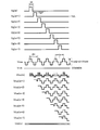
- FIG. 9 shows a display state when the liquid crystal display device described in Patent Document 3 is a four-primary color display device having a stripe arrangement and is driven by one-dot inversion. Also, waveforms of various voltages (signals) for obtaining the display state shown in FIG. 9 are shown in FIGS.
- An example will be described in which (1 ⁇ p ⁇ rp, 1 ⁇ q ⁇ cq) has two subpixels SPa (p, q) and SPb (p, q).
- 9 shows source bus lines S-C1, S-C2, S-C3, S-C4... S-Ccq, gate bus lines G-L1, G-L2, G-L3,... G-Lrp.
- FIG. 8 is a schematic diagram schematically showing (8 rows ⁇ 8 columns).
- a plurality of pixels P constitutes a plurality of color display pixel P CD
- each color display pixel P CD is composed of first, second, third and fourth pixels arranged in the row direction Has been.
- Y pixel, R pixel, G pixel, and the B pixel one color display pixel P CD is an example that is configured.
- one pixel P (p, q) has subpixels SPa (p, q) and SPb (p, q) above and below a gate bus line G-Lp that penetrates horizontally around the center of the pixel. have. That is, the subpixels SPa (p, q) and SPb (p, q) are arranged in the column direction in each pixel.
- One of the auxiliary capacitance electrodes (not shown) of each of the subpixels SPa (p, q) and SPb (p, q) is connected to the adjacent CS bus line CS-A or CS-B.
- the source bus line S-Cq for supplying a signal voltage corresponding to the display image to each pixel P (p, q) is provided so as to extend vertically (in the column direction) between the pixels in the drawing.
- the signal voltage is supplied to TFTs (not shown) included in the subpixels (pixels) on the right side of each source bus line.
- the configuration shown in FIG. 9 is a configuration in which one sub-pixel is shared by one CS bus line or one gate bus line, and has an advantage that the aperture ratio of the pixel is high.
- one-dot inversion driving can be performed.
- a case where all pixels display a certain halftone is taken up.
- FIG. 10A shows the waveform of the display signal voltage supplied to the source bus lines S-C1, S-C3, S-C5... (A group of odd-numbered source bus lines may be referred to as SO).
- FIG. 10B shows source bus lines S-C2, S-C4, S-C6... (A group of even-numbered source bus lines may be called SE).
- the display signal voltage waveform supplied FIG. 10C shows the auxiliary capacitor counter voltage waveform supplied to the CS bus line CS-A
- FIG. 10D shows the auxiliary capacitor counter voltage supplied to the CS bus line CS-B.
- FIG. 10E shows the waveform of the gate signal voltage supplied to the gate bus line GL1, FIG.
- FIG. 10F shows the waveform of the gate signal voltage supplied to the gate bus line GL2, and FIG. Gate signal supplied to the gate bus line GL3
- FIG. 10 (h) shows the waveform of the gate signal voltage supplied to the gate bus line GL4
- FIG. 10 (i) shows the waveform of the gate signal voltage supplied to the gate bus line GL5,
- FIG. 10 (j) Indicates gate signal voltage waveforms supplied to the gate bus line G-L6, respectively.
- the period from the time when the voltage of a certain gate bus line is switched from the low level (VgL) to the high level (VgH) until the time when the voltage of the next gate bus line is switched from VgL to VgH is one horizontal scanning period (1H ).
- a period in which the voltage of each gate bus line is at a high level (VgH) may be referred to as a selection period PS.
- the display signal voltages (source signal voltages) shown in FIGS. 10A and 10B are all vibration waveforms having a constant amplitude. It has become.
- the oscillation cycle of the display signal voltage is two horizontal scanning periods (2H), and the polarity of the display signal voltage is inverted for each row.
- the phase of the voltage waveform of the source bus line S0 (S-C1, S-C3%)
- the voltage waveform of the source bus line SE S-C2, S-C4.
- the polarity of the display signal voltage is inverted every column. As a result, 1-dot inversion driving is realized.
- the counter voltage is set so that the voltage waveform of the source bus line becomes approximately the center value of the voltage waveform after being supplied to the subpixel electrode.
- a symbol + is used for a signal voltage corresponding to a voltage whose voltage waveform of the sub-pixel electrode is higher than the counter voltage, and a signal voltage corresponding to a voltage whose voltage waveform of the pixel electrode is lower than the counter voltage.
- the symbol- is added.
- the symbols “+” and “ ⁇ ” correspond to the direction of the electric field applied to the liquid crystal layer, and the direction of the electric field applied to the liquid crystal layer is reversed between + and ⁇ .
- the TFT connected to this gate bus line is turned on, and the corresponding display signal voltage is supplied to the sub-pixel connected to this TFT.
- the auxiliary capacitor counter voltage changes after the voltage of the gate bus line becomes VgL, and the change amount (including the change direction and the sign of the change amount) of the auxiliary capacitor counter voltage is the same for the two sub-pixels. Since they are different from each other, the effective voltage applied to the liquid crystal layer of the sub-pixel changes.
- both the amplitude and period of the oscillation of the auxiliary capacitor counter voltage of the CS bus lines CS-A and CS-B have the same value, for example, the amplitude is Twice Vad (see FIG. 10), the period is 1H, and when the phase of one of the vibration waveforms of CS-A and CS-B is shifted by 180 degrees, it coincides with the other vibration waveform. That is, the phase is shifted by 0.5H.
- the average voltage of each subpixel electrode is When the voltage is higher than the display signal voltage of the corresponding source bus line when the voltage is VgH and the initial voltage change of the corresponding CS bus line is lowered, the response when the voltage of the corresponding gate bus line is VgH Lower than the display signal voltage of the source bus line.
- the effective voltage applied to the liquid crystal layer when the voltage change of the CS bus line is increasing is: The voltage change is higher than that in the decreasing direction.
- the symbol attached to the display signal voltage in FIG. 10A and FIG. 10B is ⁇
- the effective voltage applied to the liquid crystal layer when the voltage change of the CS bus line is increasing is The change is lower than that in the decreasing direction.
- FIG. 9 shows the state of each pixel P (p, q) and sub-pixels SPa (p, q) and SPb (p, q) in a certain vertical scanning period (hereinafter referred to as a frame period).
- the state of each subpixel is indicated by the following three symbols symmetrically written on the gate bus line corresponding to each subpixel.
- the first symbol H or L indicates the magnitude relationship of the effective applied voltage of the sub-pixel, the symbol H indicates that the effective applied voltage is high, and the symbol L indicates that the effective applied voltage is low.
- the second symbol + or ⁇ indicates the magnitude relationship between the voltage of the counter electrode and the subpixel electrode, that is, the direction of the electric field applied to the liquid crystal layer of each subpixel, and the symbol + is greater than the voltage of the counter electrode.
- the sub-pixel electrode voltage is high, and the symbol-indicates that the sub-pixel electrode voltage is lower than the counter electrode voltage.
- the third symbol A or B indicates that the corresponding CS bus line is CS-A or CS-B, respectively.
- the state of the sub-pixels SPa (1, 1) and SPb (1, 1) of the pixel P (1, 1) is examined.
- the display signal voltage in the period in which GL-1 is selected (period PS that is VgH) is “+”.
- the gate signal voltage of GL-1 changes from VgH to VgL
- the voltage of the CS bus line corresponding to each subpixel is indicated by the arrows (first from the left in FIGS. 10C and 10D). It is in the position indicated by the arrow. Therefore, the first voltage change of the auxiliary capacitor counter voltage of SPa (1, 1) after the gate signal voltage of GL-1 changes from VgH to VgL is increased (this is shown in FIG.
- the display signal voltage during the period in which GL-2 is selected is “ ⁇ ”. is there.
- the gate signal voltage of GL-2 changes from VgH to VgL
- the voltage of the CS bus line corresponding to each subpixel is indicated by the arrows (second from the left in FIGS. 10C and 10D). It is in the position indicated by the arrow. Therefore, as can be seen from FIG. 10D, the first voltage change of the auxiliary capacitor counter voltage of SPa (2, 1) after the gate signal voltage of GL-1 changes from VgH to VgL decreases (" D ").
- phase of the voltage waveform of each source bus line (SO (FIG. 10 (a)) or SE (FIG. 10 (b))) is set to 180 respectively in the frame next to the frame shown in FIG.
- AC driving in which the direction of the electric field applied to the liquid crystal layer is reversed every frame period can be achieved.
- the magnitude relationship of the effective applied voltages of the sub-pixels in each pixel in other words, the arrangement in the display screen of the order of the luminance magnitude of the sub-pixels (the positions of the symbols “H” and “L” in FIG. 9).
- the phase of the voltage waveform of the CS bus lines CS-A and CS-B is also shifted by 180 degrees as the phase of the voltage waveform of the source bus line is shifted. Good.
- a state in which the symbol “+” and the symbol “ ⁇ ” in FIG. 9 are exchanged is realized (for example, (+, H) ⁇ ( ⁇ , H) , (+, L) ⁇ ( ⁇ , L)).
- symbols “+” and “ ⁇ ” indicating the polarity (electric field direction) of each pixel are, for example, (+, ⁇ ), (+, ⁇ ) in the row direction (horizontal direction), For example, (+, ⁇ ), (+, ⁇ ), (+, ⁇ ), (+) are also inverted in the column direction (vertical direction). ,-) And 2 pixels (2 rows). That is, 1-dot inversion is realized in pixel units.
- a sub-pixel having a high luminance order that is, a bright sub-pixel having a symbol “H” in FIG.
- polarity inversion is not seen as + H, + H, + H, but in the column direction, for example, when the first column is viewed, (+ H, -H), ( The polarity is inverted at a cycle of + H, ⁇ H), (+ H, ⁇ H), (+ H, ⁇ H) and 2 pixels (2 rows). That is, line inversion is realized when viewed in units of sub-pixels with a high luminance order.
- the dark subpixels marked with the symbol L are also arranged with the same regularity.
- FIG. 3 is a diagram schematically showing a display state when the liquid crystal display device 100A of the first embodiment is driven by 1-dot inversion.
- FIG. 3 corresponds to FIG. 9 and uses the same symbols.
- the liquid crystal display device 100A of the first embodiment has the pixel structure shown in FIG. 1 and FIG.
- the difference between the display state shown in FIG. 3 and the display state shown in FIG. 9 is constituted by the polarity distribution of the pixels in the fifth column to the eighth column and the accompanying pixels in the fifth column to the eighth column. This is an arrangement in the column direction of bright sub-pixels in a color display pixel.
- the polarities of the display signal voltages supplied from S-C5 to S-C8 are applied to the pixels in the fifth to eighth columns, and S-C1 is applied to the pixels in the first to fourth columns. This is obtained by reversing the polarity of the display signal voltage supplied from S-C4.
- the pixel arrangement in two color display pixels adjacent to each other in the row direction is Y (+), R ( ⁇ ), G (+), B ( ⁇ ), Y ( ⁇ ), R (+), G ( ⁇ ), and B (+).
- the position of the bright subpixel in the column direction is Y (upper), R (lower), and G (upper).
- B (lower), Y (lower), R (upper), G (lower), and B (upper) That is, the arrangement in the column direction of the bright subpixel and the dark subpixel in the two color display pixels adjacent to each other is reversed.
- the bright subpixels of the four primary colors Y, G, R, and B are all included in the upper side in the column direction in the two color display pixels adjacent to each other in the row direction. Also, all the bright subpixels of the four primary colors Y, G, R, and B are included. Therefore, when displaying a halftone achromatic (gray) straight line parallel to the row direction, the upper edge is displayed by the bright subpixels of the four primary colors, and the lower edge is also displayed by the bright subpixels of the four primary colors. Is displayed. Therefore, unlike the multi-pixel drive of Patent Document 3, the straight edges do not appear to be colored.
- the bright subpixels of the four primary colors are included in the two color pixels adjacent to each other in the row direction, but the embodiment of the present invention is not limited to this.
- the row including the bright subpixels may include all the bright subpixels of the four primary colors.
- the two adjacent color display pixels include all the bright subpixels of the four primary colors because it is difficult to visually recognize the color blur over the entire display area.
- the polarities of the display signal voltages supplied to the adjacent pixels are opposite to each other, and the polarity is inverted for each column.
- the polarity is reversed for each row.
- the polarities of the display signal voltages are equal to each other, but polarity inversion for each column is not realized. Since a polarity distribution equivalent to that of inversion driving is obtained, flicker does not occur.
- liquid crystal display device 100A according to the second embodiment of the present invention can solve the above problem.
- FIG. 4 is a diagram illustrating waveforms of various voltages (signals) for driving the liquid crystal display device 100A according to the second embodiment of the present invention, and includes gate signal voltages Vg (m) to Vg (m + 7), CS signals. Voltages Vcsa and Vcsb, and voltages Vlca (m) to Vlca (m + 7) and Vlcb (m) applied to the liquid crystal layer of the sub-pixel are shown. Vlca (m) to Vlca (m + 7) indicate the waveform of the voltage applied to the liquid crystal layer of the bright subpixel, and the waveform of the voltage applied to the liquid crystal layer of the dark subpixel is the same regardless of the pixel row. , Only Vlcb (m) is shown. Note that one-dot inversion driving can be performed by using the display signal voltage having the waveform shown in FIGS. 10A and 10B as the display signal voltage supplied to the source bus line.
- the voltage waveform of the oscillating voltage Vcsa supplied to the CS bus line 24a (corresponding to the bright subpixel) of the liquid crystal display device 100A of the second embodiment includes at least three potentials.
- the three or more potentials include two potentials that define the maximum amplitude Vcsa (pp) of the oscillating voltage (corresponding to 2Vadd described above) and one potential that matches the average potential of the oscillating voltage.
- the “average potential of the oscillating voltage” means an effective average value of the oscillating voltage, not a simple average value of the two potentials that define the maximum amplitude of the oscillating voltage.
- the area of the portion higher than the average potential and the area of the lower portion are equal to each other in one cycle.
- the oscillating voltage exemplified below has a symmetrical waveform with respect to the center line between two potentials defining the maximum amplitude, a simple average of the two potentials defining the maximum amplitude of the oscillating voltage. The value is consistent with the effective average value of the oscillating voltage.
- the TFT connected to the pixel connected to the CS bus line to which the oscillating voltage is supplied is turned off during the time (flat portion) in which the oscillating voltage exhibits a potential that matches the average potential of the oscillating voltage waveform. It is trying to become.
- the moment when the gate bus line voltage becomes VgL and the TFT is turned off is set to the middle of the time when the average potential of the oscillating voltage is exhibited.
- the vibration voltage waveform is composed of the three potentials is shown. However, as long as the three potentials are included, the vibration voltage waveform has potentials of 5 potentials, 7 potentials, 9 potentials, and so on. Also good.
- the effective voltage V1 applied to the liquid crystal layer of the bright subpixel is a time average of values obtained by time-integrating the square of the amplitude of the hatched portion of Vlca (m) shown in FIG. 4 (the effective voltage is one vertical scanning period). Required).
- the effective voltage V2 applied to the liquid crystal layer of the dark sub-pixel is a root mean square of values obtained by integrating the squares of the amplitudes of the hatched portions of Vlcb (m) shown in FIG. Therefore, the effective voltage V1 is larger than the effective voltage V2 because the vibration voltage is superimposed on the display signal voltage, and this does not depend on the polarity of the display vibration voltage.
- the moment when the gate bus line voltage becomes VgL and the TFT is turned off is within the period in which the average potential of the oscillating voltage is present and is set to be exactly in the middle of the period. It is possible to prevent the average value of the voltage applied to the liquid crystal layer of the sub-pixel from fluctuating due to the influence of the vibration voltage. With respect to this point, the entire disclosure of JP-A-2005-99746 is incorporated herein by reference for reference.
- the moment when the TFT is turned off is set to be exactly the center of the period during which the average potential of the oscillating voltage is exhibited, but the moment when the TFT is turned off is the oscillating voltage.
- the average value of the voltage applied to the liquid crystal layer can be made substantially constant as long as the average potential is exhibited.
- the potential of the oscillating voltage at the moment when the TFT is turned off is preferably the average value of the oscillating voltage as described above. However, if the potential is between two potentials that define the maximum amplitude, at least The display state shown in FIGS. 6A and 6B can be obtained.
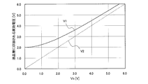
- FIG. 5 is a graph showing the relationship between the effective voltages V1 and V2 applied to the liquid crystal layer of each sub-pixel with respect to the display signal voltage Vs when an oscillating voltage having an amplitude of 2 Vadd is applied.
- the value of 2Vadd was set so that the value of V1 was 2V when the display signal voltage was 0 volts. As the value of 2Vadd is increased, the value of V1 is increased.
- V1 approaches the value of the display signal voltage as the value of the display signal voltage increases.
- V2 is always equal to the value of the display signal voltage. That is, V1 and V2 in the liquid crystal display device 100A have the relationship shown in FIG. 7 as in the liquid crystal display device of Patent Document 3, and the viewing angle dependency of the ⁇ characteristic is improved also in the liquid crystal display device 100A. You can see that
- FIG. 6A schematically shows a display state when the liquid crystal display device 100A of the second embodiment is driven by one-dot inversion.
- FIG. 6A corresponds to FIG. 9 described above, and uses the same symbols.
- the subpixel SPa corresponding to the CS bus line CS-A to which the oscillating voltage Vcsa is supplied regardless of the polarity of the display signal voltage.
- the bright subpixel is arranged on the upper side in the column direction in the pixel
- the bright subpixel is arranged on the lower side in the column direction in the pixel.
- the position in the column direction of the bright sub-pixels in the pixel alternates up and down for each row because it adopts a configuration in which one CS bus line is shared by adjacent pixels in the column direction, If two CS bus lines are provided for each pixel, for example, the bright sub-pixel can be arranged on the upper side in the column direction in all the pixels (see FIG. 6B).
- the arrangement in the column direction of the bright subpixel and the dark subpixel in any two color display pixels adjacent to each other is the same, and in all color display pixels,
- the bright subpixels of the four primary colors Y, G, R, and B are all included on the upper side in the column direction.
- the dark subpixels of the four primary colors Y, G, R, and B are naturally included on the lower side of the column direction. All pixels are included. Therefore, when displaying a halftone achromatic (gray) line parallel to the row direction, the upper edge is displayed by the bright subpixels of the four primary colors, and the lower edge is also displayed by the dark subpixels of the four primary colors. Is displayed. Therefore, unlike the multi-pixel drive of Patent Document 3, the straight edges do not appear to be colored.
- the bright sub-pixels are arranged in a checkered pattern. Focusing on the pixel rows, the bright sub-pixels are arranged in a zigzag manner along the row direction in accordance with the polarity arrangement of the display signal voltage applied to the liquid crystal layer of the pixel. That is, in a pixel having a bright subpixel located on the upper side in the column direction and adjacent to the row direction, the bright subpixel is located on the lower side in the column direction. Therefore, there is a problem that when a straight line parallel to the row direction is displayed, the straight line appears blurred.
- the liquid crystal display device 100A of the second embodiment focusing on a row of a certain pixel, the positions in the column direction of the bright sub-pixels in the pixel are arranged in a straight line. Therefore, there is no problem that the straight line appears blurred when a straight line parallel to the row direction is displayed.
- symbols “+” and “ ⁇ ” indicating the polarity (electric field direction) of each pixel are, for example, (+, ⁇ ), (+, ⁇ ) in the row direction (horizontal direction). ), (+, ⁇ ) And inversion with a period of 2 pixels (2 columns), and in the column direction (vertical direction), for example, (+, ⁇ ), (+, ⁇ ), (+, ⁇ ) , (+, ⁇ ) And 2 pixels (2 rows). That is, 1-dot inversion is realized in pixel units.
- subpixels having a high luminance order that is, subpixels with a symbol “H” in FIG. 6A.
- the polarity is inverted at a cycle of (+ H, ⁇ H), (+ H, ⁇ H), (+ H, ⁇ H) and 2 pixels (2 rows).
- the column direction for example, when looking at the first column, (+ H, -H), (+ H, -H), (+ H, -H), (+ H, -H), (+ H, -H) and a period of 2 pixels (2 rows)
- the polarity is reversed. That is, 1-dot inversion is realized even in units of sub-pixels with a high luminance order.
- the sub-pixels with the symbol L are also arranged with the same regularity.
- the liquid crystal display device 100A according to the second embodiment also disperses the polarities of the voltages applied to the liquid crystal layer in smaller units than the liquid crystal display device described in Patent Document 3 shown in FIG. Thus, it can be seen that flicker hardly occurs.
- FIG. 6B schematically shows a display state when the one-dot inversion driving is performed on the liquid crystal display device 100B using the signal voltage described above for the liquid crystal display device 100A. Since the liquid crystal display device 100B does not have the auxiliary capacitor 22b of the liquid crystal display device 100A, the CS signal voltage Vcb is not necessary.
- FIG. 6B differs from FIG. 6A in that the position of the bright subpixel in the pixel in the column direction is constant (upper side in this case). ing. Also in the liquid crystal display device 100B, 1-dot inversion driving is realized both in pixel units and in bright subpixel units. In the liquid crystal display device 100B, the position of the bright subpixel in the pixel in the column direction is constant for all the pixels. That is, the arrangement of the bright subpixel and the dark subpixel in the two pixels adjacent to each other in the row direction is the same, and the arrangement of the bright subpixel and the dark subpixel in the two pixels adjacent to each other in the column direction is Are the same.
- the display state of FIG. 6B has higher spatial resolution than the display state of FIG. 6A. If the auxiliary capacitor 22b of the dark sub-pixel cannot be omitted, the display state of FIG. 6B can be obtained by providing two CS bus lines for each pixel in the liquid crystal display device 100A as described above. .
- the liquid crystal display devices 100A and 100B according to the second embodiment of the present invention select the sub-pixel that supplies the oscillating voltage regardless of the polarity of the display signal voltage, thereby forming the sub-pixel that becomes the bright sub-pixel. This has the advantage that a pixel can be selected.
- the embodiment of the present invention is not limited to the case of four primary colors, and an even number of primary color pixels in the row direction. It can be applied to a liquid crystal display device having a stripe arrangement having Moreover, although the example using yellow, red, blue, and green was shown as four primary colors, it is not restricted to this. In the case of the four primary colors, for example, cyan, magenta, or white may be used instead of yellow. When yellow is used, there is an advantage that the color reproduction range can be expanded without imitating the display luminance. If white is used, the color reproduction range cannot be widened, but the display luminance can be increased.
- the areas of the four primary colors need not be the same. For example, the areas of the yellow and green pixels may be smaller than the areas of the red and blue pixels.
- the vibration period of the vibration voltage Vcsa is 2H
- the waveform becomes dull due to the CR time constant of the CS bus line (approximate value of the load impedance of the CS bus line).
- the period of the oscillating voltage can be extended while satisfying the above conditions.
- the entire disclosure of Japanese Patent No. 4104639 is incorporated herein by reference.
- the multi-pixel driving is not necessarily performed for all the gradations, and a necessary gradation, for example, 96 gradations or less or 64 gradations or less when performing 256 gradation display from 0 to 255 gradations.
- Multi-pixel driving may be performed only when low gradation display is performed.
- the viewing angle dependence of the ⁇ characteristic of the normally black mode liquid crystal display device is remarkable at low gradations, and thus the viewing angle dependence of the ⁇ characteristic can be improved even if such a driving method is adopted.
- the row direction is the horizontal direction of the display surface
- the column direction is the vertical direction, but this may be reversed. That is, the gate bus lines may be arranged to extend in the vertical direction, and the source bus lines may be arranged to extend in the horizontal direction. In other words, the row direction and the column direction in the above description may be interchanged. Further, although the case where the CS bus line is parallel to the gate bus line is illustrated, the CS bus line may be parallel to the source bus line.
- the present invention is not limited to the MVA type liquid crystal display device, and can be widely applied to, for example, PSA (Polymer Sustained Alignment) type, RTN type (also referred to as VATN type), IPS type and FSS type liquid crystal display devices.
- PSA Polymer Sustained Alignment
- RTN type also referred to as VATN type
- IPS type and FSS type liquid crystal display devices.
Landscapes
- Engineering & Computer Science (AREA)
- Chemical & Material Sciences (AREA)
- Crystallography & Structural Chemistry (AREA)
- Physics & Mathematics (AREA)
- Computer Hardware Design (AREA)
- General Physics & Mathematics (AREA)
- Theoretical Computer Science (AREA)
- Liquid Crystal (AREA)
- Liquid Crystal Display Device Control (AREA)
- Control Of Indicators Other Than Cathode Ray Tubes (AREA)
- Devices For Indicating Variable Information By Combining Individual Elements (AREA)
Abstract
Description
Vlca=Vs-Vd
Vlcb=Vs-Vd
となる。また、このとき、それぞれのCSバスラインの電圧Vcsa、Vcsbは
Vcsa=Vcom-Vad
Vcsb=Vcom+Vad
である。 Next, when the voltage Vg of the
Vlca = Vs−Vd
Vlcb = Vs−Vd
It becomes. At this time, the voltages Vcsa and Vcsb of the respective CS bus lines are Vcsa = Vcom−Vad.
Vcsb = Vcom + Vad
It is.
Vlca=Vs-Vd+2×K×Vad
Vlcb=Vs-Vd-2×K×Vad
へ変化する。但し、K=CCS/(CLC(V)+CCS)である。 At time T3, the voltage Vcsa of the
Vlcb = Vs−Vd−2 × K × Vad
To change. However, K = CCS / (CLC (V) + CCS).
Vlca=Vs-Vd+2×K×Vad
Vlcb=Vs-Vd-2×K×Vad
から、
Vlca=Vs-Vd
Vlcb=Vs-Vd
へ変化する。 At time T4, Vcsa changes from Vcom + Vad to Vcom−Vad, Vcsb changes from Vcom−Vad to Vcom + Vad by a factor of two, Vlca and Vlcb also
Vlca = Vs−
Vlcb = Vs−Vd−2 × K × Vad
From
Vlca = Vs−Vd
Vlcb = Vs−Vd
To change.
Vlca=Vs-Vd
Vlcb=Vs-Vd
から、
Vlca=Vs-Vd+2×K×Vad
Vlcb=Vs-Vd-2×K×Vad
へ変化する。 At time T5, Vcsa changes from Vcom−Vad to Vcom + Vad, Vcsb changes from Vcom + Vad to Vcom−Vad by a factor of two, Vlca and Vlcb also
Vlca = Vs−Vd
Vlcb = Vs−Vd
From
Vlca = Vs−
Vlcb = Vs−Vd−2 × K × Vad
To change.
Vlca=Vs-Vd+K×Vad
Vlcb=Vs-Vd-K×Vad
となる。 Vcsa, Vcsb, Vlca, and Vlcb alternately repeat the changes in T4 and T5 at intervals of an integral multiple of the horizontal writing time (horizontal scanning period) 1H. Whether the repetition interval of T4 and T5 is set to 1 time, 1 time, 2 times, 3 times, or more than 1H depends on the driving method (polarity inversion method, etc.) of the liquid crystal display device and the display state ( It is set appropriately in view of flickering, display roughness, etc. This repetition is continued when the
Vlca = Vs−Vd + K × Vad
Vlcb = Vs−Vd−K × Vad
It becomes.
V1=Vlca-Vcom
V2=Vlcb-Vcom
すなわち、
V1=Vs-Vd+K×Vad-Vcom
V2=Vs-Vd-K×Vad-Vcom
となる。 Therefore, the effective voltages V1 and V2 applied to the liquid crystal layers of the
V1 = Vlca-Vcom
V2 = Vlcb-Vcom
That is,
V1 = Vs−Vd + K × Vad−Vcom
V2 = Vs−Vd−K × Vad−Vcom
It becomes.
10a、10b 副画素
12 ゲートバスライン
13a、13b 液晶容量
14 ソースバスライン
16a、16b TFT
18a、18b 副画素電極
22a、22b 補助容量
24a、24b CSバスライン
100A,100B 液晶表示装置 10
18a,
Claims (10)
- 行および列を有するマトリクス状に配列された複数の画素であって、前記複数の画素のそれぞれは、列方向に配列された第1副画素および第2副画素を有し、前記第1副画素および前記第2副画素の一方は、少なくともある階調において他方よりも高い輝度を呈する明副画素であり、前記他方は暗副画素である、複数の画素を有し、
前記複数の画素は、複数のカラー表示画素を構成しており、前記複数のカラー表示画素のそれぞれは、行方向に配列された第1、第2、第3および第4画素を含む偶数個の画素を有し、
任意の画素の行において、前記明副画素を含む副画素の行は、前記第1、第2、第3および第4画素のそれぞれの明副画素を含む、液晶表示装置。 A plurality of pixels arranged in a matrix having rows and columns, each of the plurality of pixels having a first subpixel and a second subpixel arranged in a column direction, and the first subpixel And one of the second subpixels is a bright subpixel that exhibits higher brightness than the other at least in a certain gradation, and the other is a dark subpixel, and has a plurality of pixels.
The plurality of pixels constitute a plurality of color display pixels, and each of the plurality of color display pixels includes an even number of pixels including first, second, third, and fourth pixels arranged in a row direction. Have pixels,
The liquid crystal display device according to any one of the pixel rows, wherein the row of the sub-pixel including the bright sub-pixel includes the respective bright sub-pixels of the first, second, third, and fourth pixels. - 任意の画素の行において、互いに隣接する任意の2つのカラー表示画素における前記明副画素と前記暗副画素との列方向における配置は互いに逆である、請求項1に記載の液晶表示装置。 2. The liquid crystal display device according to claim 1, wherein, in an arbitrary row of pixels, the arrangement in the column direction of the bright subpixel and the dark subpixel in any two adjacent color display pixels is opposite to each other.
- 複数のソースバスラインであって、それぞれがある列の画素に関連付けられている複数のソースバスラインと、
複数のゲートバスラインであって、それぞれがある行の画素に関連付けられている複数のゲートバスラインと、
複数のTFTであって、それぞれが前記複数の画素のそれぞれが有する第1副画素および第2副画素の一方に関連付けられている複数のTFTと、
複数の第1CSバスラインであって、それぞれがある画素が有する前記第1副画素に関連付けられている複数の第1CSバスラインと、
複数の第2CSバスラインであって、それぞれがある画素が有する前記第1副画素に関連付けられている複数の第2CSバスラインと
を有し、
前記第1副画素は、第1副画素電極と、液晶層と、前記液晶層を介して前記第1副画素電極に対向する対向電極とによって形成された液晶容量、および、前記第1副画素電極に電気的に接続された第1補助容量電極と、絶縁層と、前記絶縁層を介して前記第1補助容量電極に対向する第1補助容量対向電極とによって形成された第1補助容量を有し、
前記第2副画素は、第2副画素電極と、液晶層と、前記液晶層を介して前記第2副画素電極に対向する対向電極とによって形成された液晶容量、および、前記第2副画素電極に電気的に接続された第2補助容量電極と、絶縁層と、前記絶縁層を介して前記第2補助容量電極に対向する第2補助容量対向電極とによって形成された第2補助容量を有し、
前記第1副画素および第2副画素のそれぞれに対応する前記TFTがオン状態にあるときに、前記第1および前記第2副画素電極と、前記第1および第2補助容量対向電極とに、それぞれ対応するソースバスラインから表示信号電圧が供給され、前記TFTがオフ状態とされた後に、前記第1および第2補助容量対向電極の電圧が変化し、その変化の方向および変化の大きさによって規定される変化量が前記第1副画素と前記第2副画素とで異なり、
任意のカラー表示画素において、互いに隣接する画素に供給される表示信号電圧の極性は互いに逆であり、且つ、任意の画素の行において、互いに隣接する任意の2つのカラー表示画素が有する前記第1、第2、第3および第4画素に供給される表示信号電圧の極性は互いに逆である、請求項2に記載の液晶表示装置。 A plurality of source bus lines, each of which is associated with a column of pixels;
A plurality of gate bus lines, each of which is associated with a row of pixels;
A plurality of TFTs, each of which is associated with one of the first and second subpixels of each of the plurality of pixels;
A plurality of first CS bus lines, each of which is associated with the first sub-pixel of a certain pixel;
A plurality of second CS bus lines, each having a plurality of second CS bus lines associated with the first subpixel of a certain pixel,
The first subpixel includes a liquid crystal capacitor formed by a first subpixel electrode, a liquid crystal layer, and a counter electrode facing the first subpixel electrode through the liquid crystal layer, and the first subpixel. A first auxiliary capacitance formed by a first auxiliary capacitance electrode electrically connected to the electrode, an insulating layer, and a first auxiliary capacitance counter electrode facing the first auxiliary capacitance electrode via the insulating layer; Have
The second subpixel includes a liquid crystal capacitor formed by a second subpixel electrode, a liquid crystal layer, and a counter electrode facing the second subpixel electrode through the liquid crystal layer, and the second subpixel. A second auxiliary capacitance formed by a second auxiliary capacitance electrode electrically connected to the electrode, an insulating layer, and a second auxiliary capacitance counter electrode facing the second auxiliary capacitance electrode via the insulating layer; Have
When the TFT corresponding to each of the first subpixel and the second subpixel is in an ON state, the first and second subpixel electrodes, and the first and second auxiliary capacitor counter electrodes, After the display signal voltage is supplied from the corresponding source bus line and the TFT is turned off, the voltages of the first and second storage capacitor counter electrodes change, depending on the direction and magnitude of the change. The prescribed change amount differs between the first subpixel and the second subpixel,
In any color display pixel, the polarities of display signal voltages supplied to pixels adjacent to each other are opposite to each other, and any two color display pixels adjacent to each other in a row of any pixel have the first. The liquid crystal display device according to claim 2, wherein polarities of display signal voltages supplied to the second, third, and fourth pixels are opposite to each other. - 任意の画素の行において、互いに隣接する任意の2つのカラー表示画素における前記明副画素と前記暗副画素との列方向における配置は同一である、請求項1に記載の液晶表示装置。 2. The liquid crystal display device according to claim 1, wherein in a row of arbitrary pixels, the arrangement in the column direction of the bright sub-pixel and the dark sub-pixel in any two color display pixels adjacent to each other is the same.
- 複数のソースバスラインであって、それぞれがある列の画素に関連付けられている複数のソースバスラインと、
複数のゲートバスラインであって、それぞれがある行の画素に関連付けられている複数のゲートバスラインと、
複数のTFTであって、それぞれが前記複数の画素のそれぞれが有する第1副画素および第2副画素の一方に関連付けられている複数のTFTと、
複数の第1CSバスラインであって、それぞれがある画素が有する前記第1副画素に関連付けられている複数の第1CSバスラインと
をさらに有し、
前記第1副画素は、第1副画素電極と、液晶層と、前記液晶層を介して前記第1副画素電極に対向する対向電極とによって形成された液晶容量、および、前記第1副画素電極に電気的に接続された第1補助容量電極と、絶縁層と、前記絶縁層を介して前記第1補助容量電極に対向する第1補助容量対向電極とによって形成された第1補助容量を有し、
前記第2副画素は、第2副画素電極と、前記液晶層を介して前記第2副画素電極に対向する対向電極とによって形成された液晶容量を有し、
対応する前記第1CSバスラインを介して前記第1補助容量対向電極に供給される第1CS信号電圧は、1垂直走査期間よりも短い周期を有する振動電圧であって、最大振幅を規定する第1電位および第2電位と、前記第1電位と前記第2電位との間の第3電位を含む少なくとも3つの電位をとり、任意の行の画素に関連付けられた前記ゲートバスラインに供給されるゲート信号電圧がハイからローに切り替わる時、対応する前記第1CSバスラインに供給される前記第1CS信号電圧は第3電位にある、請求項4に記載の液晶表示装置。 A plurality of source bus lines, each of which is associated with a column of pixels;
A plurality of gate bus lines, each of which is associated with a row of pixels;
A plurality of TFTs, each of which is associated with one of the first and second subpixels of each of the plurality of pixels;
A plurality of first CS bus lines, each of which has a plurality of first CS bus lines associated with the first subpixel of a certain pixel;
The first subpixel includes a liquid crystal capacitor formed by a first subpixel electrode, a liquid crystal layer, and a counter electrode facing the first subpixel electrode through the liquid crystal layer, and the first subpixel. A first auxiliary capacitance formed by a first auxiliary capacitance electrode electrically connected to the electrode, an insulating layer, and a first auxiliary capacitance counter electrode facing the first auxiliary capacitance electrode via the insulating layer; Have
The second subpixel has a liquid crystal capacitance formed by a second subpixel electrode and a counter electrode facing the second subpixel electrode through the liquid crystal layer,
The first CS signal voltage supplied to the first auxiliary capacitor counter electrode via the corresponding first CS bus line is an oscillating voltage having a cycle shorter than one vertical scanning period, and defines a first amplitude. A gate that takes at least three potentials including a potential, a second potential, and a third potential between the first potential and the second potential, and is supplied to the gate bus line associated with a pixel in an arbitrary row The liquid crystal display device according to claim 4, wherein when the signal voltage is switched from high to low, the first CS signal voltage supplied to the corresponding first CS bus line is at a third potential. - 前記第3電位は、前記第1電位と前記第2電位の平均値である、請求項5に記載の液晶表示装置。 The liquid crystal display device according to claim 5, wherein the third potential is an average value of the first potential and the second potential.
- 複数の第2CSバスラインであって、それぞれがある画素が有する前記第2副画素に関連付けられている複数の第2CSバスラインをさらに有し、
前記第2副画素は、前記第2副画素電極に電気的に接続された第2補助容量電極と、絶縁層と、前記絶縁層を介して前記第2補助容量電極に対向する第2補助容量対向電極とによって形成された第2補助容量を有し、
対応する前記第2CSバスラインを介して前記第2補助容量対向電極に供給される第2CS信号電圧は、1垂直走査期間の間一定である、請求項5または6に記載の液晶表示装置。 A plurality of second CS bus lines, each further comprising a plurality of second CS bus lines associated with the second sub-pixel of a certain pixel;
The second subpixel includes a second auxiliary capacitance electrode electrically connected to the second subpixel electrode, an insulating layer, and a second auxiliary capacitance facing the second auxiliary capacitance electrode through the insulating layer. A second auxiliary capacitor formed by the counter electrode;
7. The liquid crystal display device according to claim 5, wherein a second CS signal voltage supplied to the second storage capacitor counter electrode via the corresponding second CS bus line is constant during one vertical scanning period. 8. - 前記第2CS信号電圧は、前記対向電圧に供給される対向電圧と等しい、請求項7に記載の液晶表示装置。 The liquid crystal display device according to claim 7, wherein the second CS signal voltage is equal to a counter voltage supplied to the counter voltage.
- 前記第2副画素は補助容量を有しない、請求項5または6に記載の液晶表示装置。 The liquid crystal display device according to claim 5 or 6, wherein the second sub-pixel has no auxiliary capacitance.
- 前記第1、第2、第3および第4画素は、黄画素、シアン画素、マゼンタ画素および白色画素のいずれか1つと、赤画素、青画素および緑画素とを含む、請求項1から9のいずれかに記載の液晶表示装置。 The first, second, third, and fourth pixels each include one of a yellow pixel, a cyan pixel, a magenta pixel, and a white pixel, and a red pixel, a blue pixel, and a green pixel. The liquid crystal display device according to any one of the above.
Priority Applications (4)
| Application Number | Priority Date | Filing Date | Title |
|---|---|---|---|
| JP2012501863A JP5284535B2 (en) | 2010-02-26 | 2011-02-24 | Liquid crystal display |
| EP11747474.2A EP2541310B1 (en) | 2010-02-26 | 2011-02-24 | Liquid crystal display device |
| CN201180010378.4A CN102844700B (en) | 2010-02-26 | 2011-02-24 | Liquid crystal display device |
| US13/581,052 US9129569B2 (en) | 2010-02-26 | 2011-02-24 | Liquid crystal display device |
Applications Claiming Priority (2)
| Application Number | Priority Date | Filing Date | Title |
|---|---|---|---|
| JP2010042311 | 2010-02-26 | ||
| JP2010-042311 | 2010-02-26 |
Publications (1)
| Publication Number | Publication Date |
|---|---|
| WO2011105514A1 true WO2011105514A1 (en) | 2011-09-01 |
Family
ID=44506916
Family Applications (1)
| Application Number | Title | Priority Date | Filing Date |
|---|---|---|---|
| PCT/JP2011/054185 WO2011105514A1 (en) | 2010-02-26 | 2011-02-24 | Liquid crystal display device |
Country Status (5)
| Country | Link |
|---|---|
| US (1) | US9129569B2 (en) |
| EP (1) | EP2541310B1 (en) |
| JP (1) | JP5284535B2 (en) |
| CN (1) | CN102844700B (en) |
| WO (1) | WO2011105514A1 (en) |
Cited By (4)
| Publication number | Priority date | Publication date | Assignee | Title |
|---|---|---|---|---|
| CN102902071A (en) * | 2011-07-29 | 2013-01-30 | 三星电子株式会社 | Automatic three-dimensional (3D) display device |
| CN102944955A (en) * | 2012-11-05 | 2013-02-27 | 深圳市华星光电技术有限公司 | Liquid crystal display panel and display device employing same |
| WO2014087781A1 (en) * | 2012-12-07 | 2014-06-12 | 堺ディスプレイプロダクト株式会社 | Liquid crystal display device and method for driving said liquid crystal display device |
| CN108109587A (en) * | 2017-12-18 | 2018-06-01 | 惠科股份有限公司 | The driving method and driving device of display panel |
Families Citing this family (17)
| Publication number | Priority date | Publication date | Assignee | Title |
|---|---|---|---|---|
| WO2011105503A1 (en) * | 2010-02-26 | 2011-09-01 | シャープ株式会社 | Liquid crystal display device |
| US20140204008A1 (en) * | 2013-01-24 | 2014-07-24 | Au Optionics Corporation | Pixel and sub-pixel arrangement in a display panel |
| CN104298042A (en) * | 2014-09-23 | 2015-01-21 | 合肥鑫晟光电科技有限公司 | Display panel and display device |
| KR20160074804A (en) * | 2014-12-18 | 2016-06-29 | 삼성디스플레이 주식회사 | LIQUID CRYSTAL DISPLAY DEVICE having white pixel |
| CN104460114B (en) * | 2014-12-26 | 2018-01-23 | 深圳市华星光电技术有限公司 | Liquid crystal display panel and display device |
| US20160203798A1 (en) * | 2015-01-13 | 2016-07-14 | Vastview Technology Inc. | Liquid crystal display device having at least three electrodes in each pixel area |
| CN106486055B (en) * | 2015-09-02 | 2021-05-18 | 天马微电子股份有限公司 | Display device |
| TWI594228B (en) * | 2016-10-24 | 2017-08-01 | 友達光電股份有限公司 | Display device |
| CN106920527B (en) * | 2017-05-05 | 2018-02-02 | 惠科股份有限公司 | A kind of driving method of display panel, drive device and display device |
| CN107505744A (en) * | 2017-08-25 | 2017-12-22 | 惠科股份有限公司 | Liquid crystal display device |
| CN107886924B (en) * | 2017-12-19 | 2020-07-14 | 惠科股份有限公司 | Display panel, display device and driving method |
| CN108091310B (en) * | 2017-12-19 | 2019-12-10 | 惠科股份有限公司 | Display panel, display device and driving method |
| CN108109599B (en) * | 2017-12-19 | 2019-12-10 | 惠科股份有限公司 | Display panel, display device and driving method |
| CN108333841B (en) * | 2018-02-13 | 2021-04-09 | 厦门天马微电子有限公司 | Display panel, display device and driving method thereof |
| US10796651B2 (en) | 2018-09-13 | 2020-10-06 | Chongqing Hkc Optoelectronics Technology Co., Ltd. | Driving method and device of display panel, and display device |
| CN108831405B (en) * | 2018-09-13 | 2020-09-11 | 重庆惠科金渝光电科技有限公司 | Driving method, device and equipment of display panel and storage medium |
| TWI738441B (en) * | 2020-07-29 | 2021-09-01 | 友達光電股份有限公司 | Display device |
Citations (10)
| Publication number | Priority date | Publication date | Assignee | Title |
|---|---|---|---|---|
| JPH11242225A (en) | 1997-06-12 | 1999-09-07 | Fujitsu Ltd | Liquid crystal display device |
| JP2000155317A (en) | 1998-09-18 | 2000-06-06 | Fujitsu Ltd | Liquid crystal display device |
| JP2004062146A (en) | 2002-06-06 | 2004-02-26 | Sharp Corp | Liquid crystal display |
| US6879364B1 (en) | 1998-09-18 | 2005-04-12 | Fujitsu Display Technologies Corporation | Liquid crystal display apparatus having alignment control for brightness and response |
| JP2005099746A (en) | 2003-08-25 | 2005-04-14 | Sharp Corp | Liquid crystal display device and its driving method |
| JP2006285238A (en) * | 2005-03-30 | 2006-10-19 | Chi Mei Optoelectronics Corp | Display method for use in display device and display device |
| WO2007148519A1 (en) * | 2006-06-19 | 2007-12-27 | Sharp Kabushiki Kaisha | Display apparatus |
| JP4104639B2 (en) | 2004-12-28 | 2008-06-18 | シャープ株式会社 | Liquid crystal display device and driving method thereof |
| JP2008164667A (en) * | 2006-12-27 | 2008-07-17 | Sharp Corp | Liquid crystal display device and driving method thereof |
| WO2009034714A1 (en) * | 2007-09-13 | 2009-03-19 | Sharp Kabushiki Kaisha | Multiple-primary-color liquid crystal display device |
Family Cites Families (11)
| Publication number | Priority date | Publication date | Assignee | Title |
|---|---|---|---|---|
| TW200528891A (en) * | 2004-02-23 | 2005-09-01 | Shih-Hsien Tseng | Image display device |
| KR100721907B1 (en) * | 2005-07-25 | 2007-05-28 | 삼성전자주식회사 | Display device |
| KR101383714B1 (en) * | 2005-12-02 | 2014-04-09 | 삼성디스플레이 주식회사 | Liquid crystal display |
| KR101035737B1 (en) | 2006-03-15 | 2011-05-20 | 샤프 가부시키가이샤 | Active matrix substrate, display device and television receiver |
| CN101563646B (en) * | 2006-12-26 | 2012-11-07 | 夏普株式会社 | Liquid crystal panel, liquid crystal display device, and television device |
| TWI348065B (en) | 2007-01-10 | 2011-09-01 | Au Optronics Corp | Liquid crystal display |
| CN100480796C (en) | 2007-01-22 | 2009-04-22 | 友达光电股份有限公司 | Structure of liquid crystal display |
| JP4943505B2 (en) * | 2007-04-26 | 2012-05-30 | シャープ株式会社 | Liquid crystal display |
| WO2008139766A1 (en) * | 2007-05-14 | 2008-11-20 | Sharp Kabushiki Kaisha | Display device and display method thereof |
| CN101800035A (en) * | 2009-02-05 | 2010-08-11 | 瀚宇彩晶股份有限公司 | Liquid crystal display device and driving method thereof |
| KR101127593B1 (en) * | 2010-04-07 | 2012-03-23 | 삼성모바일디스플레이주식회사 | Liquid crystal display device |
-
2011
- 2011-02-24 CN CN201180010378.4A patent/CN102844700B/en not_active Expired - Fee Related
- 2011-02-24 US US13/581,052 patent/US9129569B2/en active Active
- 2011-02-24 JP JP2012501863A patent/JP5284535B2/en not_active Expired - Fee Related
- 2011-02-24 WO PCT/JP2011/054185 patent/WO2011105514A1/en active Application Filing
- 2011-02-24 EP EP11747474.2A patent/EP2541310B1/en not_active Not-in-force
Patent Citations (12)
| Publication number | Priority date | Publication date | Assignee | Title |
|---|---|---|---|---|
| JPH11242225A (en) | 1997-06-12 | 1999-09-07 | Fujitsu Ltd | Liquid crystal display device |
| US6724452B1 (en) | 1997-06-12 | 2004-04-20 | Fujitsu Display Technologies Corporation | Vertically aligned (VA) liquid crystal display device |
| JP2000155317A (en) | 1998-09-18 | 2000-06-06 | Fujitsu Ltd | Liquid crystal display device |
| US6879364B1 (en) | 1998-09-18 | 2005-04-12 | Fujitsu Display Technologies Corporation | Liquid crystal display apparatus having alignment control for brightness and response |
| JP2004062146A (en) | 2002-06-06 | 2004-02-26 | Sharp Corp | Liquid crystal display |
| US6958791B2 (en) | 2002-06-06 | 2005-10-25 | Sharp Kabushiki Kaisha | Liquid crystal display |
| JP2005099746A (en) | 2003-08-25 | 2005-04-14 | Sharp Corp | Liquid crystal display device and its driving method |
| JP4104639B2 (en) | 2004-12-28 | 2008-06-18 | シャープ株式会社 | Liquid crystal display device and driving method thereof |
| JP2006285238A (en) * | 2005-03-30 | 2006-10-19 | Chi Mei Optoelectronics Corp | Display method for use in display device and display device |
| WO2007148519A1 (en) * | 2006-06-19 | 2007-12-27 | Sharp Kabushiki Kaisha | Display apparatus |
| JP2008164667A (en) * | 2006-12-27 | 2008-07-17 | Sharp Corp | Liquid crystal display device and driving method thereof |
| WO2009034714A1 (en) * | 2007-09-13 | 2009-03-19 | Sharp Kabushiki Kaisha | Multiple-primary-color liquid crystal display device |
Cited By (8)
| Publication number | Priority date | Publication date | Assignee | Title |
|---|---|---|---|---|
| CN102902071A (en) * | 2011-07-29 | 2013-01-30 | 三星电子株式会社 | Automatic three-dimensional (3D) display device |
| CN102902071B (en) * | 2011-07-29 | 2017-06-09 | 三星电子株式会社 | Autostereoscopic 3D display device |
| CN102944955A (en) * | 2012-11-05 | 2013-02-27 | 深圳市华星光电技术有限公司 | Liquid crystal display panel and display device employing same |
| WO2014067197A1 (en) * | 2012-11-05 | 2014-05-08 | 深圳市华星光电技术有限公司 | Liquid crystal display panel and display device applying same |
| WO2014087781A1 (en) * | 2012-12-07 | 2014-06-12 | 堺ディスプレイプロダクト株式会社 | Liquid crystal display device and method for driving said liquid crystal display device |
| US9564095B2 (en) | 2012-12-07 | 2017-02-07 | Sakai Display Products Corporation | Liquid crystal display device and method for driving the liquid crystal display device whereby shadowing can be prevented |
| CN108109587A (en) * | 2017-12-18 | 2018-06-01 | 惠科股份有限公司 | The driving method and driving device of display panel |
| CN108109587B (en) * | 2017-12-18 | 2020-09-25 | 惠科股份有限公司 | Driving method and driving device of display panel |
Also Published As
| Publication number | Publication date |
|---|---|
| CN102844700A (en) | 2012-12-26 |
| US20120327135A1 (en) | 2012-12-27 |
| US9129569B2 (en) | 2015-09-08 |
| CN102844700B (en) | 2015-05-13 |
| JP5284535B2 (en) | 2013-09-11 |
| EP2541310A4 (en) | 2014-01-29 |
| JPWO2011105514A1 (en) | 2013-06-20 |
| EP2541310A1 (en) | 2013-01-02 |
| EP2541310B1 (en) | 2017-11-29 |
Similar Documents
| Publication | Publication Date | Title |
|---|---|---|
| JP5284535B2 (en) | Liquid crystal display | |
| KR100798746B1 (en) | Liquid crystal display | |
| KR100711230B1 (en) | Liquid crystal display | |
| US7791577B2 (en) | Liquid crystal display device and method for driving the same | |
| US8638282B2 (en) | Liquid crystal display device | |
| JP5042270B2 (en) | Liquid crystal display | |
| JP5043847B2 (en) | Liquid crystal display | |
| JP5631968B2 (en) | Liquid crystal display | |
| US20160155407A1 (en) | Active matrix display device and method of driving same | |
| JP2006171342A (en) | Liquid crystal display device |
Legal Events
| Date | Code | Title | Description |
|---|---|---|---|
| WWE | Wipo information: entry into national phase |
Ref document number: 201180010378.4 Country of ref document: CN |
|
| 121 | Ep: the epo has been informed by wipo that ep was designated in this application |
Ref document number: 11747474 Country of ref document: EP Kind code of ref document: A1 |
|
| REEP | Request for entry into the european phase |
Ref document number: 2011747474 Country of ref document: EP |
|
| WWE | Wipo information: entry into national phase |
Ref document number: 2012501863 Country of ref document: JP Ref document number: 2011747474 Country of ref document: EP |
|
| WWE | Wipo information: entry into national phase |
Ref document number: 13581052 Country of ref document: US |
|
| NENP | Non-entry into the national phase |
Ref country code: DE |