WO2011096258A1 - Magnetic pattern detection device - Google Patents
Magnetic pattern detection device Download PDFInfo
- Publication number
- WO2011096258A1 WO2011096258A1 PCT/JP2011/050449 JP2011050449W WO2011096258A1 WO 2011096258 A1 WO2011096258 A1 WO 2011096258A1 JP 2011050449 W JP2011050449 W JP 2011050449W WO 2011096258 A1 WO2011096258 A1 WO 2011096258A1
- Authority
- WO
- WIPO (PCT)
- Prior art keywords
- magnetic
- sensor element
- medium
- magnetic sensor
- signal
- Prior art date
Links
Images


Classifications
-
- G—PHYSICS
- G07—CHECKING-DEVICES
- G07D—HANDLING OF COINS OR VALUABLE PAPERS, e.g. TESTING, SORTING BY DENOMINATIONS, COUNTING, DISPENSING, CHANGING OR DEPOSITING
- G07D7/00—Testing specially adapted to determine the identity or genuineness of valuable papers or for segregating those which are unacceptable, e.g. banknotes that are alien to a currency
- G07D7/04—Testing magnetic properties of the materials thereof, e.g. by detection of magnetic imprint
-
- G—PHYSICS
- G07—CHECKING-DEVICES
- G07D—HANDLING OF COINS OR VALUABLE PAPERS, e.g. TESTING, SORTING BY DENOMINATIONS, COUNTING, DISPENSING, CHANGING OR DEPOSITING
- G07D7/00—Testing specially adapted to determine the identity or genuineness of valuable papers or for segregating those which are unacceptable, e.g. banknotes that are alien to a currency
- G07D7/20—Testing patterns thereon
Definitions
- the present invention relates to a magnetic pattern detection device for detecting a magnetic pattern of a medium such as an object to which a magnetic material is attached or a banknote printed with magnetic ink.
- the magnetic sensor element detects changes in magnetic flux when the medium passes.
- the signal processing unit performs signal processing on the sensor output signal output from the magnetic sensor element.
- the signal processing unit includes an amplifying unit configured by an amplifier to which a sensor output signal and a reference voltage composed of a constant voltage are input. After the sensor output signal is amplified by the amplifying unit, various signal processes are performed. (See Patent Documents 1 to 3).
- the magnetic sensor element detects a change in magnetic flux when the medium passes, and detects a magnetic pattern based on a signal output from the magnetic sensor element.
- the magnetic sensor element is, for example, a channel in the column direction Y (medium width direction) orthogonal to the moving direction X (row direction) of the medium 1. Twenty pieces are arranged for CH1 to CH20. By scanning the twenty magnetic sensor elements 40 in the column direction Y, a magnetic pattern is detected from the entire width direction of the medium 1.
- the magnetic sensor element 40 shown in FIGS. 18A and 18B are scanned once, data is detected in each of the 20 magnetic sensor elements 40 of the channels CH1 to CH20.
- the magnetic sensor element 40 is converted into a detection data digital signal in the magnetic sensor element 40 by an A / D converter in synchronization with the timing when the magnetic sensor element 40 is in the ON state, the magnetic field for one column of the medium 1 is obtained. A pattern can be detected.
- the magnetic sensor element 40 is excited by an excitation signal having a frequency of 500 kHz.
- the medium 1 moves in the row direction X.
- the area where the magnetic sensor element 40 is located in the on state is shown as a hatched area, and the magnetic sensor element 40 is located in the on state during the current scan in the medium 1.
- the next magnetic sensor element 40 is in an ON state in a region adjacent to the moving direction X (region with a downward slanting line) on the opposite side to the moving direction X (region with a slanting line to the right) become. Therefore, the magnetic pattern can be detected from the entire medium 1.
- a magnetic pattern detection apparatus that scans a plurality of magnetic sensor elements 40 arranged in the column direction Y and moves the medium 1, the moving speed of the medium 1 and the magnetic sensor elements 40 in the moving direction X of the medium 1 Depending on the dimensions and the scanning speed, as shown in FIG. 18C, the area where the magnetic sensor element 40 is located in the ON state at the time of the current scan (the area with a diagonal line rising to the right) and the next time A gap G is generated between the area where the magnetic sensor element 40 is located in the ON state during scanning (an area with a slanting line to the right).
- the medium 1 moves 0.32 mm while one scan is completed.
- the dimension in the moving direction of the magnetic sensor element 1 is 0.3 mm, the area where the magnetic sensor element 40 is located in the ON state during the current scan and the magnetic sensor element 40 during the next scan.
- a gap G of 0.02 mm is generated between the region where was positioned in the ON state. For this reason, in the area corresponding to the gap G in the medium 1, the magnetic characteristics cannot be detected by the magnetic sensor element 40, and it is difficult to accurately detect the magnetic pattern from the entire surface of the medium 1.
- the magnetic sensor element 40 since the magnetic sensor element 40 normally has a sensing range that is equal to or larger than the projection area of the magnetic sensor element 40 with respect to the medium 1, if the gap G can be covered by such a sensing range, a magnetic pattern can be generated from the entire surface of the medium 1. Even in such a case, depending on the moving speed of the medium 1, the size of the sensing range of the magnetic sensor element 40 in the moving direction X of the medium 1, and the scanning speed, It is difficult to avoid the occurrence of the gap G between the sensing range in the next scan.
- the first object of the present invention is to provide a magnetic pattern detection device capable of improving the gain without significantly increasing the cost.
- the second problem of the present invention is that even when a method of scanning a plurality of magnetic sensor elements arranged in the column direction and moving the medium relative to the magnetic sensor is employed, the magnetic field is reliably detected from the entire surface of the medium.
- An object of the present invention is to provide a magnetic pattern detection device capable of detecting a pattern.
- the present invention provides a magnetic sensor element that detects a magnetic characteristic of a medium, and a signal processing unit that detects a magnetic pattern of the medium based on a detection result of the magnetic sensor element.
- the signal processing unit includes an amplification unit that amplifies a sensor output signal output from the magnetic sensor element excited by an excitation signal, and the amplification unit outputs the sensor output.
- the reference voltage that changes in conjunction with the excitation signal is used, so that the difference between the sensor output signal output from the magnetic sensor element and the reference voltage is small. Therefore, the amplifier gain can be increased and the S / N ratio can be increased without adding a cost-increasing circuit such as a bridge circuit. Further, since the reference voltage changes in conjunction with the excitation signal and is synchronized with the sensor output signal, the sensor output signal can be appropriately amplified.
- the reference voltage is preferably a signal having a waveform obtained by differentiating the excitation signal. Since the sensor output signal corresponds to the time differentiation of the magnetic flux generated by the excitation signal, if the waveform signal obtained by differentiating the excitation signal is used as the reference voltage for the amplifier, the difference between the sensor output signal and the reference voltage is small. Can be increased.
- the reference voltage generation unit includes a CR differentiation circuit that differentiates the excitation signal to generate the reference voltage. If comprised in this way, the differentiation circuit which differentiates an excitation signal and produces
- the reference voltage generation unit may include a dummy magnetic sensor element that is excited by the excitation signal and outputs a signal obtained by differentiating the excitation signal as the reference voltage.
- the output signal from the dummy magnetic sensor element corresponds to the time differentiation of the magnetic flux generated by the excitation signal, and a waveform signal obtained by differentiating the excitation signal can be generated as a reference voltage. Further, with such a reference voltage, the difference from the sensor output signal is extremely small, so that the gain can be increased.
- the signal processing unit includes: a first integrating circuit that integrates a signal component having a positive polarity in a signal output from the amplifier; and a second integrating circuit that integrates a signal component having a negative polarity. It is preferable to provide. With this configuration, even when the pulse width of the signal output from the amplifier is narrow, the signal component having a positive polarity and the signal component having a negative polarity can be integrated to convert an amplitude change into an area change. Therefore, the apparent gain can be increased with a simple configuration.
- Another embodiment of the present invention is a magnetic pattern detection device having a magnetic sensor element that detects a magnetic characteristic of a medium, and a signal processing unit that detects a magnetic pattern of the medium based on a detection result of the magnetic sensor element.
- the signal processing unit includes a first integration circuit that integrates a signal component having a positive polarity in the sensor output, and a second integration circuit that integrates a signal component having a negative polarity. It is characterized by.
- a signal component having a positive polarity and a signal component having a negative polarity can be integrated to convert an amplitude change into an area change. Can increase the apparent gain.
- the magnetic sensor element preferably includes a plurality of coils for outputting the sensor output signal as a differential output. This configuration has the advantage that it is less susceptible to disturbances.
- the present invention includes a magnetic sensor element that detects magnetic characteristics from a medium, and a transport mechanism that moves the medium relative to the magnetic sensor element.
- a magnetic sensor element that detects magnetic characteristics from a medium
- a transport mechanism that moves the medium relative to the magnetic sensor element.
- the magnetic pattern detection device a plurality of the magnetic sensor elements are arranged in a row direction orthogonal to the moving direction of the medium, and the moving speed of the medium by the transport mechanism is v (mm / ⁇ sec)
- T dimension of the magnetic sensor element in the moving direction
- N the number of scans per unit time ta ( ⁇ sec) of the magnetic sensor element in the column direction
- the moving speed v and the unit time ta, the dimension T, and the number of scans N are the following conditional expressions (v ⁇ ta) ⁇ (T ⁇ N)
- N is characterized by satisfying an integer of 2 or more.
- the moving speed v of the medium, the dimension T in the moving direction of the magnetic sensor element, and the number of scans N per unit time ta of the magnetic sensor element in the column direction are set so as to satisfy the above conditional expression.
- the unit time ta is one scanning period for detecting a magnetic pattern for one column of the medium, and the data obtained by the magnetic sensor element by scanning performed during the one scanning period is used as the unit time ta. Based on this, it is possible to adopt a configuration in which a magnetic pattern for one column of the medium is detected. That is, a plurality of scans are performed during one scan period for detecting a magnetic pattern for one column. For this reason, it is possible to adopt a configuration that detects a magnetic pattern for one column based on data obtained by a plurality of scans, and according to such a configuration, noise or the like is included in any of the data obtained by the magnetic sensor element. Even when the influence is included, the influence of the noise can be reduced.
- a magnetic field corresponding to one column of the medium based on data obtained by the magnetic sensor element by one scan or a plurality of scans out of N scans performed during the one scan period.
- a configuration in which a pattern is detected can be employed. With this configuration, an optimum operation can be realized according to the type of medium, the detection accuracy required for the magnetic pattern detection device, and the like.
- a magnetic pattern for one column of the medium is detected based on data obtained by the magnetic sensor element by a plurality of scans out of N scans performed during the one scan period. It is preferable. With this configuration, the magnetic characteristics of the medium can be detected with high accuracy. Even if any of the data obtained by the magnetic sensor element includes the influence of noise or the like, the influence of the noise can be mitigated.
- the present invention it is possible to adopt a configuration in which a magnetic pattern for one column of the medium is detected based on all data obtained by the magnetic sensor element by N scans performed during the one scan period.
- the area where the magnetic sensor element is projected to the medium at the same magnification partially overlaps in the current scan and the next scan, so that the magnetic characteristics of the medium can be detected with high accuracy.
- the influence of the noise can be mitigated.
- the present invention employs a configuration in which a magnetic pattern for one column of the medium is detected based on data obtained by the magnetic sensor element by a part of N scans performed during one scanning period. May be.
- a region in which the magnetic sensor element is projected at the same magnification on the medium partially overlaps in the moving direction in the current scan and the next scan.
- a plurality of data obtained by the magnetic sensor element by scanning two or more times and less than N times, or an area where the magnetic sensor element is projected at the same magnification on the medium is moved in the current scan and the next scan.
- a configuration in which a magnetic pattern for one column of the medium is detected based on a plurality of data obtained by the magnetic sensor element by scanning at least twice and less than N times contacting without overlapping in the direction may be adopted. Good.
- an area in which the magnetic sensor element is projected at the same magnification on the medium is partially in the moving direction between the current scan and the next scan. It is preferable that a magnetic pattern for one column of the medium is detected based on a plurality of data obtained by the magnetic sensor element by two or more overlapping scans and less than N scans. With this configuration, the area where the magnetic sensor element is projected to the medium at the same magnification partially overlaps in the current scan and the next scan, so that the magnetic characteristics of the medium can be detected with high accuracy. . Even if any of the data obtained by the magnetic sensor element includes the influence of noise or the like, the influence of the noise can be mitigated.
- the sensing range in the moving direction of the magnetic sensor element is larger than the dimension T in the moving direction of the magnetic sensor element, the sensing range is N out of N scans performed during the one scanning period.
- a plurality of data obtained by the magnetic sensor element by two or more scans and less than N scans partially overlapping in the moving direction in the current scan and the next scan, or the sensing range This scan and the next scan
- a configuration in which a magnetic pattern for one row of the medium is detected based on a plurality of data obtained by the magnetic sensor element by scanning two times or more and less than N times in contact with each other without overlapping in the moving direction. It may be adopted.
- the sensing range is obtained by performing the scan twice or more and less than N times partially overlapping in the moving direction in the current scan and the next scan. It is preferable that a magnetic pattern for one row of the medium is detected based on a plurality of data obtained by the magnetic sensor element. With this configuration, since the sensing range partially overlaps between the current scan and the next scan, the magnetic characteristics of the medium can be detected with high accuracy. Even if any of the data obtained by the magnetic sensor element includes the influence of noise or the like, the influence of the noise can be mitigated.
- an averaging process is performed on the plurality of data. It is preferable. With this configuration, even when a magnetic pattern for one column of the medium is detected from a plurality of data, simple processing is sufficient. In addition, by averaging a plurality of data, even if any of the data obtained by the magnetic sensor element includes the influence of noise or the like, the influence of the noise can be reduced.
- the excitation signal when the magnetic sensor element is excited by an excitation signal and outputs a signal, the excitation signal is added to a signal output by each of the plurality of magnetic sensor elements during a single scan for a plurality of cycles. It is preferable to have a frequency including a signal component by the excitation signal.
- each signal output from each of the plurality of magnetic sensor elements during one scan includes a signal component due to excitation signals for a plurality of cycles, so that the magnetic characteristics of the medium can be accurately determined. Can be detected.
- the reference voltage that changes in conjunction with the excitation signal is used.
- the difference is small. Therefore, the amplifier gain can be increased and the S / N ratio can be increased without adding a cost-increasing circuit such as a bridge circuit. Further, since the reference voltage changes in conjunction with the excitation signal, the sensor output signal and the reference voltage are synchronized, so that the sensor output signal can be appropriately amplified.
- the signal processing unit includes a first integration circuit that integrates a signal component having a positive polarity in the sensor output, and a signal component having a negative polarity.
- 2nd integration circuit that integrates, so even if the pulse width of the sensor output signal is narrow, the signal component with positive polarity and the signal component with negative polarity are each integrated to convert the amplitude change into area change can do. Therefore, the apparent gain can be increased with a simple configuration.
- the moving speed v of the medium, the dimension T in the moving direction of the magnetic sensor element, and the number of scans N per unit time ta of the magnetic sensor element in the column direction are (V ⁇ ta) ⁇ (T ⁇ N)
- N is set so as to satisfy an integer of 2 or more, the area where the magnetic sensor element is located in the on state at the time of the current scan and the magnetic sensor element in the on state at the next scan No gap is generated between the region located at Therefore, even when a plurality of magnetic sensor elements arranged in the column direction are scanned and the medium is moved relative to the magnetic sensor, the magnetic pattern can be reliably detected from the entire surface of the medium.
- FIG. 1 is an explanatory diagram showing the configuration of a magnetic pattern detection device including the magnetic sensor device according to the first embodiment of the present invention.
- FIGS. 1 (a) and 1 (b) are magnetic pattern detection devices. It is explanatory drawing which shows typically a principal part structure, and explanatory drawing which shows a cross-sectional structure typically.
- a magnetic pattern detection device 100 shown in FIG. 1 is a device that detects magnetism from a medium 1 such as a banknote or a securities, and performs authenticity determination or type determination.
- a sheet is detected by a roller, a guide (not shown), or the like.
- a magnetic sensor device 20 that detects magnetism from the medium 1 at an intermediate position of the medium moving path 11 by the conveying device 10.
- the roller and the guide are made of a nonmagnetic material such as aluminum.
- the magnetic sensor device 20 is disposed below the medium movement path 11, but may be disposed above the medium movement path 11. In any case, the magnetic sensor device 20 is arranged so that the sensor surface 21 faces the medium moving path 11.
- the medium 1 is provided with a magnetic pattern with magnetic ink on a narrow magnetic region 1a extending in the moving direction X of the medium 1.
- the magnetic pattern has a residual magnetic flux density Br and a permeability ⁇ .
- the medium 1 is formed with a first magnetic pattern printed with magnetic ink containing hard material and a second magnetic pattern printed with magnetic ink containing soft material. Therefore, the magnetic pattern detection apparatus 100 of the present embodiment detects the presence / absence of each magnetic pattern in the medium 1 based on both the residual magnetic flux density level and the magnetic permeability level.
- the magnetic sensor device 20 for detecting such two types of magnetic patterns is common. Therefore, the magnetic pattern detection apparatus 100 of this embodiment has the following configuration.
- FIG. 2 is an explanatory diagram of the magnetic sensor device 20 according to the first embodiment of the present invention.
- FIGS. 2A and 2B show the layout of the magnetic sensor elements and the like in the magnetic sensor device 20. It is explanatory drawing which shows, and explanatory drawing which shows direction of a magnetic sensor element.
- the magnetic sensor device 20 includes a magnetic field applying magnet 30 that applies a magnetic field to the medium 1, and a medium after the magnetic field is applied.
- 1 includes a magnetic sensor element 40 that detects a magnetic flux when a bias magnetic field is applied, and a nonmagnetic case 25 that covers the magnetic field applying magnet 30 and the magnetic sensor element 40.
- the magnetic sensor device 20 includes a sensor surface 21 that is substantially flush with the medium movement path 11, and slope portions 22 and 23 that are connected to both sides of the sensor surface 21 in the movement direction of the medium 1.
- the shape is defined by the shape of the case 25.
- the magnetic sensor device 20 extends in a direction crossing the moving direction X of the medium 1, and a plurality of magnetic field applying magnets 30 and magnetic sensor elements 40 are arranged in a direction crossing the moving direction X of the medium 1. ing. In this embodiment, the magnetic sensor device 20 extends in the medium width direction Y orthogonal to the movement direction X among the directions intersecting the movement direction X of the medium 1, and the magnetic field applying magnet 30 and the magnetic sensor element 40. Are arranged in the medium width direction Y (column direction) orthogonal to the moving direction X, and arranged in a line at equal intervals.
- the “on state” means an active state in which an excitation signal described later is applied to the magnetic sensor element 40 and signal processing is performed on a signal output from the magnetic sensor element 40.
- the magnetic field application magnet 30 is arranged as a first magnetic field application magnet 31 and a second magnetic field application magnet 32 on both sides of the moving direction X of the medium 1 with respect to the magnetic sensor element 40, and the arrow X1
- a magnetic field applying first magnet 31, a magnetic sensor element 40, and a magnetic field applying second magnet 32 are arranged in this order along the moving direction of the medium 1 shown in FIG.
- a magnetic field application second magnet 32, a magnetic sensor element 40, and a magnetic field application first magnet 31 are arranged in this order along the moving direction of the medium 1 indicated by the arrow X2, and the medium 1 is indicated by the arrow X1.
- the magnetic property of the medium 1 can be detected regardless of the direction and the direction indicated by the arrow X2.
- the magnetic sensor element 40 is disposed at an intermediate position between the first magnetic field application magnet 31 and the second magnetic field application magnet 32, and is separated from the magnetic sensor element 40 from the first magnetic field application magnet 31.
- the distance is equal to the separation distance between the magnetic field application second magnet 32 and the magnetic sensor element 40.
- the first magnetic field application magnet 31, the magnetic sensor element 40, and the second magnetic field application magnet 32 are all arranged so as to face the sensor surface 21 of the magnetic sensor device 20.
- the magnetic field application magnet 30 (the first magnetic field application magnet 31 and the second magnetic field application magnet 32) includes a permanent magnet 35 such as a ferrite or neodymium magnet.
- the permanent magnet 35 has a pole on which the side located on the sensor surface 21 is different from the side opposite to the side on which the sensor surface 21 is located. Magnetized. For this reason, in the permanent magnet 35, a surface located on the sensor surface 21 side functions as a magnetized surface 350 for the medium 1.
- the magnetic field applying first magnet 31 is changed to the medium 1.
- the medium 1 after being magnetized by the magnetic field passes through the magnetic sensor element 40.
- a magnetic field is applied to the medium 1 from the second magnetic field application magnet 32, and the medium is magnetized by the magnetic field. 1 passes through the magnetic sensor element 40.
- the plurality of permanent magnets 35 used in the magnetic field applying magnet 30 are all the same in size and shape, but are arranged in the following orientations.
- the permanent magnets 35 adjacent in the medium width direction (column direction) Y orthogonal to the moving direction X of the medium 1 are opposite to each other. Is magnetized in the direction of That is, of the plurality of permanent magnets 35 arranged in the medium width direction Y perpendicular to the moving direction X of the medium 1, one permanent magnet 35 is magnetized with an N pole at the end located on the medium moving path 11 side.
- the end located on the side opposite to the medium moving path 11 side is magnetized to the S pole, but is adjacent to the permanent magnet 35 in the medium width direction Y perpendicular to the moving direction X of the medium 1.
- the permanent magnet 35 has an end located on the medium moving path 11 side magnetized to the S pole, and an end located on the side opposite to the medium moving path 11 side magnetized to the N pole.
- the permanent magnet 35 of the first magnetic field application magnet 31 and the permanent magnet 35 of the second magnetic field application magnet 32 that face each other in the moving direction of the medium 1 have different poles across the magnetic sensor element 40.
- the permanent magnet 35 of the first magnetic field application magnet 31 and the permanent magnet 35 of the second magnetic field application magnet 32 that face each other in the moving direction of the medium 1 are arranged so that the same poles face each other across the magnetic sensor element 40. Sometimes placed.
- FIG. 3 is an explanatory diagram of the magnetic sensor element 40 used in the magnetic sensor device 20 according to the first embodiment of the present invention.
- FIGS. 3 (a), 3 (b), and 3 (c) are magnetic sensors.
- FIG. 4 is a front view of the element 40, an explanatory diagram of an excitation waveform for the magnetic sensor element 40, and an explanatory diagram of an output signal from the magnetic sensor element 40.
- 3A shows a state where the medium 1 moves in a direction perpendicular to the drawing.
- each of the magnetic sensor elements 40 has a thin plate shape, and the size in the width direction W40 is larger than the size in the thickness direction T40.
- the magnetic sensor element 40 is arranged with the thickness direction T40 facing the moving direction X of the medium 1, and the width direction W40 is oriented in the medium width direction (column direction) Y orthogonal to the moving direction X of the medium 1. ing.
- the magnetic sensor element 40 is covered with a thin plate-like nonmagnetic member 47 having a thickness of about 0.3 mm to 1.0 mm whose both surfaces are made of ceramic or the like.
- the thickness of the magnetic sensor element 40 including the nonmagnetic member 47 is also included.
- the entire direction is the thickness dimension (dimension T) of the magnetic sensor element 40.
- the magnetic sensor element 40 may be housed in a magnetic shield case (not shown). In this case, the magnetic shield case is opened at the top where the medium movement path is located, and the magnetic sensor element 40 is exposed from the magnetic shield case toward the medium movement path 11.
- the magnetic sensor element 40 includes a sensor core 41, an excitation coil 48 wound around the sensor core 41, and a sensor core. And a detection coil 49 wound around 41.
- the sensor core 41 includes a body part 42 extending in the width direction W40 of the magnetic sensor element 40, and a magnetic flux collecting protrusion 43 that protrudes from the body part 42 toward the medium moving path 11 side of the medium 1. It has.
- the magnetic flux collecting projections 43 are configured as two magnetic flux collecting projections 431 and 432 protruding from both ends of the body portion 42 in the width direction W40 toward the medium moving path 11 side of the medium 1.
- the two magnetic flux collecting projections 431 and 432 are separated in the width direction W40.
- the sensor core 41 includes a protrusion 44 that protrudes from the body 42 to the side opposite to the magnetism-collecting protrusion 43.
- the protrusion 44 has both end portions in the width direction W40 of the body 42. Are formed as two protrusions 441 and 442 protruding toward the opposite side of the medium 1 from the medium moving path 11 side.
- the exciting coil 48 is wound around a portion sandwiched by the magnetic flux collecting projections 431 and 432 in the trunk portion 42.
- the detection coil 49 is wound around the magnetic flux collecting projection 43, and in this embodiment, the detection coil 49 includes two magnetic flux collecting projections 43 (the magnetic flux collecting projections 431 and 432) of the sensor core 41.
- a detection coil 491 wound around the magnetic flux collection protrusion 431 and a detection coil 492 wound around the magnetic flux collection protrusion 432 are included.
- the two detection coils 491 and 492 are wound around the magnetic flux collecting projections 431 and 432 in opposite directions.
- the two detection coils 491 and 492 are formed by continuously winding one coil wire around the magnetic flux collecting projections 431 and 432, the two detection coils 491 and 492 are electrically connected in series. It is connected to the.
- the two detection coils 491 and 492 may be wound around the magnetic flux collecting projections 431 and 432, respectively, and then electrically connected in series.
- the thickness direction T40 perpendicular to both the width direction W40 and the projecting direction (height direction V40) of the magnetic flux collecting projection 43 is directed to the moving direction X of the medium 1.
- the width direction W40 in which the magnetic flux collecting protrusions 43 (magnetic flux collecting protrusions 431 and 432) and the detection coils 49 (detection coils 491 and 492) are separated from each other is It faces the medium width direction (column direction) Y orthogonal to the movement direction X.
- an excitation signal composed of an alternating current (see FIG. 3B) is applied to the excitation coil 48 from an excitation circuit 50 described later with reference to FIG.
- a bias magnetic field is formed around the sensor core 41, and a detection waveform signal shown in FIG. become.
- the detected waveform shown in FIG. 3C is a temporal differential signal of the magnetic flux generated by the excitation signal, and is close to the temporal differential signal of the excitation signal.
- the sensor core 41 of the magnetic sensor element 40 has a magnetic material layer 41c sandwiched between a nonmagnetic first substrate 41a and a nonmagnetic second substrate 41b, as shown in FIG. 1B. It has a structure.
- the magnetic material layer 41c is made of a thin plate-like amorphous metal foil made of an amorphous (amorphous) metal magnetic material bonded to one surface of the first substrate 41a by an adhesive layer (not shown).
- the second substrate 41b is bonded to one surface of the first substrate 41a by an adhesive layer so as to sandwich the magnetic material layer 41c therebetween.
- Each of these adhesive layers is a layer formed by solidifying a prepreg formed by impregnating a resin material into a fiber reinforcing material such as glass cloth, carbon fiber, or aramid fiber.
- a resin material an epoxy resin type or a phenol resin type is used.
- a thermosetting resin such as polyester resin is used.
- the amorphous metal foil used as the magnetic material layer 41c is formed by rolling with a roll, and examples of cobalt-based materials include Co—Fe—Ni—Mo—B—Si, Co—Fe—Ni—B—Si, and the like.
- Amorphous alloys such as Fe-B-Si, Fe-B-Si-C, Fe-B-Si-Cr, Fe-Co-B-Si, Fe-Ni-Mo-B, etc. Can be illustrated.
- the first substrate 41a and the second substrate 41b include ceramic substrates such as alumina substrates, glass substrates, and the like, and plastic substrates may be used as long as sufficient rigidity can be obtained.
- FIG. 4 is a block diagram showing an electrical configuration of the magnetic pattern detection apparatus 100 according to the first embodiment of the present invention.
- FIGS. 4A and 4B are views of the entire main part of the circuit unit. It is explanatory drawing which shows a structure, and is explanatory drawing which shows the structure of an amplifier part periphery among circuit parts.
- the circuit unit 5 shown in FIGS. 4A and 4B generally includes an excitation circuit 50 for applying the alternating current shown in FIG. 3B as an excitation signal to the excitation coil 48 and a detection coil 49. And an electrically connected signal processing unit 60.
- the excitation circuit 50 includes a plurality of excitation driver amplifiers 51 corresponding to each of the plurality of magnetic sensor elements 40 shown in FIG. 2, and a multiplexer 52 for sequentially supplying excitation signals to the plurality of excitation driver amplifiers 51.
- an amplifier 53 that generates an excitation signal from the excitation command signal, and sequentially supplies the excitation signals amplified by the excitation driver amplifier 51 to the excitation coils 48 of the plurality of magnetic sensor elements 40.
- the signal processing unit 60 generates a first signal S1 corresponding to the residual magnetic flux density level and a second signal S2 corresponding to the magnetic permeability level from the sensor output signal output from the detection coil 49 of the magnetic sensor device 20. Based on the first signal S1 and the second signal S2 and relative position information between the medium 1 and the magnetic sensor element 40, the control unit (not shown) determines whether or not there are a plurality of types of magnetic patterns in the medium 1 and The formation position is detected.
- the signal processing unit 60 amplifies the sensor output signal output from the magnetic sensor element 40, and the extraction unit extracts the peak value and the bottom value from the signal output from the amplification unit 70.
- the extraction unit 80 includes a multiplexer 81 that sequentially outputs the amplified signal output from the amplification unit 70 to the subsequent stage, a clamp circuit 82, and an offset adjustment unit 83 that performs offset adjustment of the signal output from the clamp circuit 82. ing.
- the clamp circuit 82 includes a first diode 821 that rectifies the amplified sensor output signal output from the amplification unit 70, and a polarity inversion circuit 822 that performs polarity inversion of the amplified sensor output signal output from the amplification unit 70. And a second diode 823 that rectifies the signal whose polarity is inverted in the polarity inverting circuit 822.
- the offset adjustment unit 83 includes a first offset adjustment circuit 831 for the output from the first diode 821 and a second offset adjustment circuit 832 for the output from the second diode 823, and the first offset adjustment circuit 831.
- the second offset adjustment circuit 832 includes offset adjustment reference voltage generation circuits 831a and 832a and operational amplifiers 831b and 832b.
- the extraction unit 80 includes a hold circuit 84 following the offset adjustment unit 83 and a gain setting unit 85 subsequent to the hold circuit 84.
- the hold circuit 84 includes a first peak hold circuit 841 that holds the peak value of the output signal from the first offset adjustment circuit 831, and a second peak hold circuit that holds the peak value of the output signal from the second offset adjustment circuit 832. 842.
- the second offset adjustment circuit 832 receives a signal obtained by inverting the polarity of the signal output from the amplification unit 70 by the polarity inverting circuit 822 and then rectifying the signal by the second diode 823.
- the second peak hold circuit 842 corresponds to a bottom hold circuit that holds the bottom value of the amplified signal output from the amplification unit 70.
- the gain setting unit 85 is held by the gain setting first amplifier 851 (main amplifier) and the second peak hold circuit 842 (bottom hold circuit) for setting the gain of the value held by the first peak hold circuit 841. And a gain setting second amplifier 852 (main amplifier) for setting the gain of the value.
- the values held by the first peak hold circuit 841 and the second peak hold circuit 842 are set to a predetermined gain and digitally set.
- the signal is output to the A / D converter 91 of the signal processing unit 90.
- the digital signal processing unit 90 adds the value held by the first peak hold circuit 841 and the value held by the second peak hold circuit 842 to generate the first signal S1; A subtracting circuit 93 that subtracts the value held by the peak hold circuit 841 from the value held by the second peak hold circuit 842 to generate the second signal S2.
- the digital signal processing unit 90 includes a control signal output unit 94 that outputs a switching control signal, an excitation command signal, an offset control signal, and the like.
- the digital signal processing unit 90 configured in this manner outputs a first signal S1 and a second signal S2 to a higher-level control unit (not shown). In the control unit, the first signal S1 and the second signal S2 are output. The authenticity of the medium 1 is determined based on the two signals S2.
- the upper control unit associates the first signal S1 and the second signal S2 with the relative position information between the magnetic sensor element 40 and the medium 1, and the comparison pattern recorded in advance in the recording unit. And a determination unit that determines whether the medium 1 is true or false.
- the determination unit is a predetermined unit based on a program recorded in advance in a recording unit (not shown) such as a ROM or a RAM. Processing is performed to determine whether the medium 1 is true or false.
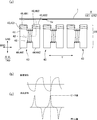
- FIG. 5 is an explanatory diagram of signals and the like input to the amplifier in the amplification unit 70 of the magnetic pattern detection device 100 according to the first embodiment of the present invention.
- FIGS. It is explanatory drawing which shows the waveform of an excitation signal, a sensor output signal, and a reference voltage, and explanatory drawing which shows the waveform after amplifying the difference of a sensor output signal and a reference voltage with an amplifier.
- the excitation signal is indicated by a solid line L1
- the sensor output signal is indicated by a solid line L2
- the reference voltage is indicated by a solid line L3
- the difference between the sensor output signal and the reference voltage is amplified.
- the signal after amplification at is indicated by a solid line L4.
- the amplification unit 70 includes a plurality of amplifiers 71 (preamplifiers) corresponding to each of the plurality of magnetic sensor elements 40 as shown in FIG. A sensor output signal output from the magnetic sensor element 40 and a reference voltage are input to 71.
- the amplification unit 70 includes a reference voltage generation unit 72 that generates, as a reference voltage, a signal that changes in conjunction with the excitation signal.
- the amplifier 71 generates the reference voltage generation unit 72. Signal is input as the reference voltage.
- the reference voltage has a waveform indicated by a solid line L3 in FIGS. 5A and 5B, and this waveform is a waveform obtained by differentiating the excitation signal indicated by the solid line L1 in FIG. Equivalent to. Therefore, the reference voltage changes in conjunction with the excitation signal.
- the reference voltage generation unit 72 is a CR differentiation circuit 73 including a capacitor C and a resistor R, and the CR differentiation circuit 73 generates a signal obtained by differentiating the excitation signal as a reference voltage. To do.
- the reference voltage obtained by differentiating the excitation signal is the sensor output signal. Synchronized with. With such a reference voltage, the difference from the sensor output signal is small as shown in FIG. 5B, so that even if the gain of the amplifier 71 is increased, as shown by the solid line L4 in FIG. The output signal from 71 does not saturate.
- FIG. 6 is an explanatory diagram showing characteristics and the like of various magnetic inks formed on the medium 1 in the magnetic pattern detection apparatus 100 according to the first embodiment of the present invention.
- FIG. 7 is an explanatory diagram showing the principle of detecting the presence / absence of a magnetic pattern from the medium 1 on which different types of magnetic patterns are formed in the magnetic pattern detection apparatus 100 according to the first embodiment of the present invention.
- the medium 1 is formed with a first magnetic pattern printed with a magnetic ink containing a hard material and a second magnetic pattern printed with a magnetic ink containing a soft material.
- the magnetic ink containing the hard material has a high level of residual magnetic flux density Br when a magnetic field is applied, as shown in FIG. 6B1 by a hysteresis loop, such as residual magnetic flux density Br and permeability ⁇ .
- the permeability ⁇ is low.
- magnetic ink containing a soft material has a low residual magnetic flux density Br when a magnetic field is applied as shown in FIG. 6 (c1), but has a high magnetic permeability ⁇ .
- the material of the magnetic ink can be determined by measuring the residual magnetic flux density Br and the magnetic permeability ⁇ . More specifically, since the magnetic permeability ⁇ has a correlation with the holding force Hc, in this embodiment, the residual magnetic flux density Br and the holding force Hc are measured, and the residual magnetic flux density Br is measured. And the holding force Hc differ depending on the magnetic ink (magnetic material). Therefore, the material of the magnetic ink can be determined. Further, the measured values of the residual magnetic flux density Br and the magnetic permeability ⁇ (holding force Hc) vary depending on the density of the ink and the distance between the medium 1 and the magnetic sensor device 20, but in this embodiment, the magnetic sensor device 20 is the same. Since the residual magnetic flux density Br and the magnetic permeability ⁇ (holding force Hc) are measured at the position, the material of the magnetic ink can be reliably determined according to the ratio of the residual magnetic flux density Br and the holding force Hc.
- the magnetic pattern detection apparatus 100 of the present embodiment when the medium 1 moves in the direction indicated by the arrow X1 and passes through the magnetic sensor apparatus 20, first, a magnetic field is applied from the first magnetic field application magnet 31 to the medium 1, and the magnetic field The medium 1 after is applied passes through the magnetic sensor element 40. Until then, the detection coil 49 of the magnetic sensor element 40 outputs a signal corresponding to the BH curve of the sensor core 41 shown in FIG. 6 (a2), as shown in FIG. 6 (a3). Accordingly, the first signal S1 output from the adding circuit 92 shown in FIG. 4 and the second signal S2 output from the subtracting circuit 93 are as shown in FIG. 6 (a4).
- the first magnetic pattern when the first magnetic pattern is formed on the medium 1 with the magnetic ink containing a hard material such as ferrite powder, the first magnetic pattern has a high level as shown in FIG. It has a residual magnetic flux density Br. Therefore, as shown in FIG. 7A1, when the medium 1 passes through the magnetic field application magnet 30, the first magnetic pattern becomes a magnet by the magnetic field from the magnetic field application magnet 30. Therefore, the signal output from the detection coil 49 of the magnetic sensor element 40 receives a direct current bias from the first magnetic pattern as shown in FIG. 6 (b2), and FIG. 6 (b3) and FIG. The waveform changes to (a2).
- the peak voltage and the bottom voltage of the signal S0 are shifted in the same direction as indicated by arrows A1 and A2, and the shift amount of the peak voltage and the shift amount of the bottom voltage are different.
- the signal S0 changes as the medium 1 moves. Therefore, the first signal S1 output from the adder circuit 92 shown in FIG. 4 is as shown in FIG. 6B4, and fluctuates every time the first magnetic pattern of the medium 1 passes through the magnetic sensor element 40. .
- the magnetic permeability ⁇ is low in the first magnetic pattern formed by the magnetic ink containing the hard material, the first magnetic pattern has an influence on the shift of the peak voltage and the bottom voltage of the signal S0. It can be considered that only the residual magnetic flux density Br. Therefore, the second signal S2 output from the subtraction circuit 93 shown in FIG. 4 does not change even when the first magnetic pattern of the medium 1 passes through the magnetic sensor element 40, and the signal shown in FIG. 6 (b4). It is the same.
- the second magnetic pattern when the second magnetic pattern is formed on the medium 1 with magnetic ink containing a soft material such as soft magnetic stainless steel powder, the hysteresis loop of the second magnetic pattern is shown in FIG. As shown, the level of the residual magnetic flux density Br is low through the inside of the hysteresis curve of the first magnetic pattern with the magnetic ink containing the hard material shown in FIG. 6 (b1). For this reason, even after the medium 1 passes through the magnetic field applying magnet 30, the second magnetic pattern has a low residual magnetic flux density Br. However, since the magnetic permeability ⁇ is high, the second magnetic pattern functions as a magnetic material as shown in FIG. For this reason, as shown in FIG.
- the signal output from the detection coil 49 of the magnetic sensor element 40 has an increase in the permeability ⁇ due to the presence of the second magnetic pattern.
- the waveform shown in FIG. 7 (b2) That is, the peak voltage of the signal S0 is shifted to the higher side as indicated by the arrow A3, while the bottom voltage is shifted to the lower side as indicated by the arrow A4. At that time, the absolute value of the shift amount of the peak voltage and the shift amount of the bottom voltage are substantially equal.
- the signal S0 changes as the medium 1 moves. Therefore, the second signal S2 output from the subtraction circuit 93 shown in FIG. 4 is as shown in FIG. 6C4, and fluctuates every time the second magnetic pattern of the medium 1 passes through the magnetic sensor element 40. .
- the second magnetic pattern formed by the magnetic ink containing the soft material since the second magnetic pattern formed by the magnetic ink containing the soft material has a low residual magnetic flux density Br, it is the second magnetic pattern that affects the shift of the peak voltage and the bottom voltage of the signal. It can be considered that only the magnetic permeability ⁇ of. Therefore, the first signal S1 output from the addition circuit 92 shown in FIG. 4 does not change even when the second magnetic pattern of the medium 1 passes through the magnetic sensor element 40, and the signal shown in FIG. 6 (c4). It is the same.
- the first signal S1 obtained by adding the peak value and the bottom value of the signal output from the magnetic sensor element 40 in the addition circuit 92 is the residual magnetic flux density level of the magnetic pattern.
- the second signal S2 obtained by subtracting the peak value and the bottom value of the signal output from the magnetic sensor element 40 in the subtraction circuit 93 is a signal corresponding to the magnetic permeability ⁇ of the magnetic pattern. If monitored, it is possible to detect the presence and position of the second magnetic pattern formed by the magnetic ink containing the soft material.
- the presence / absence and formation position of each of the magnetic patterns in the medium 1 of a plurality of types of magnetic patterns having different residual magnetic flux density Br and magnetic permeability ⁇ when a magnetic field is applied are based on both the residual magnetic flux density level and the magnetic permeability level. Can be identified.
- the amplifier 70 of the signal processing unit 60 amplifies the sensor output signal output from the magnetic sensor element 40 excited by the excitation signal and the reference voltage.
- the reference voltage generating unit 72 When inputting to 71, the reference voltage generating unit 72 generates a signal that changes in conjunction with the excitation signal, and inputs the signal to the amplifier 71 as a reference voltage. For this reason, the difference between the sensor output signal output from the magnetic sensor element 40 and the reference voltage is small. Therefore, the gain of the amplifier 71 can be increased and the S / N ratio can be increased without adding a circuit that increases costs, such as a bridge circuit. Further, since the reference voltage changes in conjunction with the excitation signal, the sensor output signal and the reference voltage are synchronized, and the sensor output signal can be appropriately amplified.
- the reference voltage generation unit 72 since the reference voltage generation unit 72 generates a signal having a waveform obtained by differentiating the excitation signal as the reference voltage, the difference between the sensor output signal and the reference voltage can be reduced. That is, since the sensor output signal corresponds to time differentiation of the magnetic flux generated by the excitation signal, if a signal having a waveform obtained by differentiating the excitation signal is used as the reference voltage of the amplifier 71, the difference between the sensor output signal and the reference voltage is small. So gain can be increased.
- the reference voltage generation unit 72 includes a CR differentiation circuit 73 that differentiates the excitation signal to generate a reference voltage, the excitation signal is differentiated by using an inexpensive electric element such as a capacitor C or a resistor R. A reference voltage can be generated.
- the common magnetic sensor device 20 detects the presence / absence and formation position of each magnetic pattern based on both the residual magnetic flux density level and the magnetic permeability level. There is no time difference between the measurement and the permeability level measurement. Therefore, even when the measurement is performed while moving the magnetic sensor device 20 and the medium 1, the signal processing unit 60 can perform highly accurate detection with a simple configuration. In addition, since the transport device 10 is also required to have running stability only at a location that passes through the magnetic sensor device 20, the configuration can be simplified.
- the medium 1 on which the magnetic pattern is formed by the magnetic ink including both the hard material and the soft material, and the material positioned between the hard material and the soft material are included.
- the magnetic pattern can also be detected for the medium 1 on which the magnetic pattern is formed with the magnetic ink. That is, as for the magnetic pattern whose magnetic characteristics are located between the first magnetic pattern and the second magnetic pattern, as shown in FIG. 6 (d1), the hysteresis loop has a hard loop as shown in FIG. 6 (b1). Since it is located between the hysteresis loop of the magnetic pattern of the material and the hysteresis loop of the magnetic pattern of the soft material shown in FIG. 6 (c1), the signal pattern shown in FIG. 6 (d4) can be obtained. In addition, the presence or absence and the formation position can be detected.
- the magnetic field application magnets 30 are arranged as the first magnetic field application magnet 31 and the second magnetic field application magnet 32 on both sides of the magnetic sensor element 40 in the moving direction of the medium 1.
- the medium 1 moving in the direction indicated by the arrow X1 is magnetized by the first magnetic field application magnet 31, and then the magnetic sensor element 40 biases the medium 1 after magnetization.
- the magnetic flux can be detected in a state where a magnetic field is applied, and the medium 1 moving in the direction indicated by the arrow X2 is magnetized by the magnetic field applying second magnet 32, and then magnetized by the magnetic sensor element 40.
- the magnetic flux in a state where a bias magnetic field is applied to the medium 1 can be detected. Therefore, if the magnetic pattern detection apparatus 100 of this embodiment is used for a depositing / dispensing machine, it is possible to determine the authenticity of the deposited medium 1 and also to determine the authenticity of the dispensed medium 1. .
- FIG. 8 is an explanatory diagram showing a configuration around the amplification unit 70 in the circuit unit of the magnetic pattern detection apparatus 100 according to the first embodiment 2 of the present invention. Since the basic configuration of this embodiment is the same as that of Embodiment 1, common portions are denoted by the same reference numerals and description thereof is omitted.
- the amplifier 70 is provided with a plurality of amplifiers 71 corresponding to each of the plurality of magnetic sensor elements 40.
- a multiplexer 77 is provided after the sensor element 40, and an amplifier 71 is provided after the multiplexer 77. Therefore, sensor output signals output from the plurality of magnetic sensor elements 40 are sequentially output to the amplifier 71 by the multiplexer 77. For this reason, there exists an advantage that the sensor output signal output from the some magnetic sensor element 40 can be amplified with one amplifier 71.
- the amplification unit 70 generates a signal that changes in conjunction with the excitation signal in the reference voltage generation unit 72 including the CR differentiation circuit 73, and the signal Is input to the amplifier 71 as a reference voltage. For this reason, since the difference between the sensor output signal output from the magnetic sensor element 40 and the reference voltage is small, the gain of the amplifier 71 can be increased without adding a cost-increasing circuit such as a bridge circuit. The same effects as those of the first embodiment are obtained.
- a plurality of excitation driver amplifiers 51 corresponding to each of the plurality of magnetic sensor elements 40 are provided.
- a multiplexer 54 is provided after the excitation driver amplifier 51.
- a plurality of magnetic sensor elements 40 are provided downstream of the multiplexer 54. Therefore, the excitation signal output from the excitation driver amplifier 51 is sequentially output to the plurality of magnetic sensor elements 40 by the multiplexer 54. For this reason, there is an advantage that an excitation signal can be supplied to a plurality of magnetic sensor elements 40 by one excitation driver amplifier 51.
- the switching timing of the multiplexer 77 may be finely adjusted in order to prevent a signal that is not originally required when switching the multiplexer 77, for example, noise generated when the detection signal is switched by the multiplexer 77 from passing through the subsequent stage.
- an analog switch 79 may be added to the output stage of the amplifier 71 so that noise or the like does not pass through the subsequent stage.
- FIG. 9 is an explanatory diagram showing a configuration of the amplifying unit 70 of the magnetic pattern detection device 100 according to the first embodiment 3 of the present invention, and FIGS. It is explanatory drawing which shows a structure, and explanatory drawing of the magnetic sensor element for dummy. Since the basic configuration of this embodiment is the same as that of the first and second embodiments, common portions are denoted by the same reference numerals and description thereof is omitted.
- the reference voltage generation unit 72 including the CR differentiation circuit 73 is used.
- a dummy magnetic sensor element 74 is provided.
- a reference voltage generator 72 is provided. Therefore, the dummy magnetic sensor element 74 can generate a signal that changes in conjunction with the excitation signal, and can input this signal to the amplifier 71 as a reference voltage.
- the dummy magnetic sensor element 74 is provided at a position separated from the medium moving path 11 shown in FIG. 1 and is not affected by the medium 1 or the magnetic sensor element 40 magnetically.
- the dummy magnetic sensor element 74 has the same configuration as the magnetic sensor element 40 described with reference to FIGS. 2B and 3B.
- the sensor core 41 has a structure in which an excitation coil 48 and a detection coil 49 are wound.
- An excitation signal is supplied to the excitation coil 48 of the dummy magnetic sensor element 74 via the dummy excitation driver amplifier 510, and an output from the detection coil 49 of the dummy magnetic sensor element 74 is used as a reference voltage for the amplifier 71. Has been supplied to.
- the dummy magnetic sensor element 74 is excited by the excitation signal and outputs a signal obtained by differentiating the excitation signal from the detection coil 49.
- the output signal from the dummy magnetic sensor element 74 corresponds to the time differentiation of the magnetic flux generated by the excitation signal, and is a waveform signal obtained by differentiating the excitation signal. For this reason, since the difference between the reference voltage and the sensor output signal can be made extremely small, the gain can be increased.
- the reference voltage generator 72 including the dummy magnetic sensor element 74 is provided based on the first embodiment 2. However, the dummy magnetic sensor element is different from the first embodiment. A reference voltage generation unit 72 having 74 may be provided.
- FIG. 10 is an explanatory diagram showing a configuration around the amplification unit 70 of the magnetic pattern detection device 100 according to the first embodiment of the present invention. Since the basic configuration of this embodiment is the same as that of the first to third embodiments, common portions are denoted by the same reference numerals and description thereof is omitted.
- the offset adjustment unit 83 is provided at the subsequent stage of the clamp circuit 82.
- the offset adjustment unit 83 includes the first offset adjustment circuit 831 as shown in FIG.
- the operational amplifier 831b and the operational amplifier 832b of the second offset adjustment circuit 832 are provided with capacitors, and the first offset adjustment circuit 831 and the second offset adjustment circuit 832 are configured as a first integration circuit 835 and a second integration circuit 836. ing.
- the first integration circuit 835 integrates a signal component having a positive polarity in the signal output from the amplifier 71
- the second integration circuit 836 integrates a signal component having a negative polarity. Therefore, even when the pulse width of the signal output from the amplifier 71 is narrow, the signal component having a positive polarity and the signal component having a negative polarity can be integrated to convert the amplitude change into an area change. The apparent gain can be increased with a simple configuration.
- the amplification unit 70 generates a signal that changes in conjunction with the excitation signal in the reference voltage generation unit 72 including the CR differentiation circuit 73, and the signal Is input to the amplifier 71 as a reference voltage. For this reason, since the difference between the sensor output signal output from the magnetic sensor element 40 and the reference voltage is small, the gain of the amplifier 71 can be increased without adding a cost-increasing circuit such as a bridge circuit. The same effects as those of the first embodiment are obtained.
- FIG. 11 is an explanatory diagram showing a configuration around the offset adjustment unit 83 of the magnetic pattern detection apparatus 100 according to the first embodiment of the present invention. Since the basic configuration of this embodiment is the same as that of the first to fourth embodiments, common portions are denoted by the same reference numerals and description thereof is omitted.
- the reference voltage generation unit 72 is provided in the amplification unit 70. However, in this embodiment, the reference voltage generation unit 72 is not provided in the amplification unit 70 as shown in FIG.
- the reference voltage of the amplifier 71 is a constant potential such as a ground potential.
- the first offset adjustment circuit 831 and the second offset adjustment circuit 832 are configured as a first integration circuit 835 and a second integration circuit 836. Therefore, the first integration circuit 835 integrates a signal component having a positive polarity in the signal output from the magnetic sensor element 40, and the second integration circuit 836 integrates a signal component having a negative polarity.
- the signal component having a positive polarity and the signal component having a negative polarity can be integrated to convert the amplitude change into an area change.
- the apparent gain can be increased with a simple configuration.
- FIG. 12 is an explanatory diagram of the magnetic sensor element 40 used in the magnetic pattern detection device 100 according to the first embodiment of the present invention. Since the basic configuration of this embodiment is the same as that of the first to first embodiments, common portions are denoted by the same reference numerals and description thereof is omitted.
- the excitation signal is applied only to the excitation coil 48 of the magnetic sensor element 40 and the detection coil 49.
- An excitation coil 48 and a detection coil 49 are connected in series, and an excitation signal is applied to the excitation coil 48 and the detection coil 49.
- an amplifier 71 is connected to a connection portion between the excitation coil 48 and the detection coil 49, and a signal is differentially output to the amplifier 71 from a connection portion between the excitation coil 48 and the detection coil 49.
- the amplification unit 70 generates a signal that changes in conjunction with the excitation signal in the reference voltage generation unit 72 including the CR differentiation circuit 73, and the signal Is input to the amplifier 71 as a reference voltage. For this reason, since the difference between the sensor output signal output from the magnetic sensor element 40 and the reference voltage is small, the gain of the amplifier 71 can be increased without adding a cost-increasing circuit such as a bridge circuit. The same effects as those of the first embodiment 1 are obtained.
- FIGS. 1, 2, 3, 6, and 7 The same configuration and characteristics as the principle of detecting the presence / absence of a magnetic pattern, such as the magnetic pattern detection device, magnetic sensor device, magnetic sensor element, and magnetic ink characteristics described in 1. can be used. Detailed description here is omitted.
- FIG. 13 is an explanatory diagram showing an electrical configuration of the magnetic pattern detection device 100 according to the second embodiment of the present invention.
- FIGS. 13 (a) and 13 (b) show the entire main part of the circuit unit. It is explanatory drawing which shows a structure, and an explanatory view which shows a mode that a some magnetic sensor element is scanned, and is sequentially in an ON state.
- the basic configuration of the circuit portion of this embodiment shown in FIG. 13A is the same as the configuration of the circuit portion of the first embodiment shown in FIG. Are described with the same reference numerals.
- the circuit section 5 shown in FIG. 13A is generally configured by an excitation circuit 50 that applies the alternating current shown in FIG. 3B to the excitation coil 48 as an excitation signal, and a detection coil 49 of the magnetic sensor element 40. (See FIG. 2B and FIG. 3A) and a signal processing unit 60 that is electrically connected.
- the excitation circuit 50 includes a plurality of excitation driver amplifiers 51 corresponding to each of the plurality of magnetic sensor elements 40 shown in FIG. 2, and a multiplexer 52 for sequentially supplying excitation signals to the plurality of excitation driver amplifiers 51. And an amplifier 53 for generating an excitation signal from the excitation command signal.
- the excitation coil 48 (see FIGS.
- the excitation driver amplifier 51 includes an excitation driver amplifier 51.
- the excitation signals after being amplified in step 1 are sequentially supplied.
- a common excitation driver amplifier 51 may be arranged for the plurality of magnetic sensor elements 40 at the subsequent stage of the multiplexer 52.
- the signal processing unit 60 generates a first signal S1 corresponding to the residual magnetic flux density level and a second signal S2 corresponding to the magnetic permeability level from the sensor output signal output from the detection coil 49 of the magnetic sensor device 20.
- the data is output to an upper control unit (not shown).
- the signal processing unit 60 includes an amplification unit 70 including an amplifier 71 that amplifies the sensor output signal output from the magnetic sensor element 40, and a peak value and a bottom value from the signal output from the amplification unit 70. And a digital signal processing unit 90 provided with an A / D converter 91.
- the extraction unit 80 includes a multiplexer 81 that sequentially outputs the amplified signal output from the amplification unit 70 to the subsequent stage, a clamp circuit 82, and an offset adjustment circuit 83 that performs offset adjustment of the signal output from the clamp circuit 82. ing.
- the clamp circuit 82 includes a first diode 821 that rectifies the amplified sensor output signal output from the amplification unit 70, and a polarity inversion circuit 822 that performs polarity inversion of the amplified sensor output signal output from the amplification unit 70. , And a second diode 823 that rectifies the signal whose polarity has been inverted in the polarity inverting circuit 822. Therefore, the offset adjustment circuit 83 includes a first offset adjustment circuit 831 for the output from the first diode 821 and a second offset adjustment circuit 832 for the output from the second diode 823, and the first offset adjustment circuit 831.
- the second offset adjustment circuit 832 includes offset adjustment reference voltage generation circuits 831a and 832a and operational amplifiers 831b and 832b.
- a common amplifier 71 may be arranged for the plurality of magnetic sensor elements 40 at the subsequent stage of the multiplexer 81.
- the extraction unit 80 includes a hold circuit 84 following the offset adjustment circuit 83 and a gain setting unit 85 subsequent to the hold circuit 84.
- the hold circuit 84 includes a first peak hold circuit 841 that holds the peak value of the output signal from the first offset adjustment circuit 831, and a second peak hold circuit that holds the peak value of the output signal from the second offset adjustment circuit 832. 842.
- the second offset adjustment circuit 832 receives a signal obtained by inverting the polarity of the signal output from the amplification unit 70 by the polarity inverting circuit 822 and then rectifying the signal by the second diode 823.
- the second peak hold circuit 842 corresponds to a bottom hold circuit that holds the bottom value of the amplified signal output from the amplification unit 70.
- the gain setting unit 85 sets the gain of the value held by the first peak hold circuit 841 and the gain of the value held by the second peak hold circuit 842 (bottom hold circuit).
- the gain setting second amplifier 852 is set, and the values held by the first peak hold circuit 841 and the second peak hold circuit 842 are set to a predetermined gain, and the A / D of the digital signal processing unit 90 is set. Output to the converter 91.
- the digital signal processor 90 adds the value held by the A / D converter 91, the first peak hold circuit 841, and the value held by the second peak hold circuit 842 to generate the first signal S1.
- the addition circuit 92 includes a subtraction circuit 93 that subtracts the value held by the first peak hold circuit 841 and the value held by the second peak hold circuit 842 to generate the second signal S2.
- the magnetic sensor element 40 outputs a plurality of signals (four signals in this embodiment) during one scanning period in order to determine the magnetic characteristics of one region on the medium 1. Therefore, the digital signal processing unit 90 includes an averaging processing unit 96 subsequent to the A / D converter 91. Therefore, the adder circuit 92 digitally signals the four values held by the first peak hold circuit 841 and the second peak hold circuit 842 by the A / D converter 91, and then the four values are averaged by the averaging processor 96. Addition processing is performed using the averaged values.
- the subtracting circuit 93 digitalizes the four values held by the first peak hold circuit 841 and the second peak hold circuit 842 by the A / D converter 91 and then averages the four values by the averaging processing unit 96. Subtraction processing is performed using the converted value.
- the digital signal processing unit 90 includes a control signal output unit 94 that outputs a switching control signal, an excitation command signal, an offset control signal, and the like.
- the switching control signal controls the multiplexers 52 and 81, and FIG.
- a plurality of magnetic sensor elements 40 arranged in the medium width direction, that is, in the column direction Y perpendicular to the row direction X, which is the moving direction of the medium 1, are arranged. This controls the scanning operation and the timing at which other circuits operate.
- the digital signal processing unit 90 configured as described above outputs a first signal S1 and a second signal S2 to a higher-level control unit (not shown).
- the first signal S1 and the second signal S2 are output.
- the authenticity of the medium 1 is determined based on the two signals S2. More specifically, the upper control unit associates the first signal S1 and the second signal S2 with the relative position information between the magnetic sensor element 40 and the medium 1, and the comparison pattern recorded in advance in the recording unit.
- a determination unit that determines whether the medium 1 is true or false.
- the determination unit is a predetermined unit based on a program recorded in advance in a recording unit (not shown) such as a ROM or a RAM. Processing is performed to determine whether the medium 1 is true or false.
- FIG. 14 is an explanatory diagram showing the scanning operation and the like of the magnetic pattern detection apparatus 100 according to the second embodiment of the present invention.
- FIG. 2 is an explanatory diagram showing a state in which the magnetic sensor elements 40 are arranged in the column direction Y, an explanatory diagram showing an enlarged layout of the magnetic sensor elements, and a magnetic sensor element that is turned on during one scanning period for each scan.
- An explanatory view showing a state where a position is moved on the medium 1 and an explanation showing an enlarged view of a state where a position where the magnetic sensor element which is in an on state is moved for each scan is moved on the medium 1 during one scan period.
- FIGS. 15A and 15B are explanatory diagrams showing the operating conditions of the circuit unit in the magnetic pattern detection apparatus 100 according to the second embodiment of the present invention.
- FIGS. 15A and 15B show the frequency and sample of the detection signal. It is explanatory drawing which shows the relationship with hold operation
- the magnetic sensor element 40 is in the column direction Y (medium width direction) orthogonal to the moving direction X of the medium 1.
- Twenty channels are arranged for the channels CH1 to CH20, and the magnetic pattern is detected from the entire width direction of the medium 1 by scanning the twenty magnetic sensor elements 40 in the column direction. That is, if a plurality of magnetic sensor elements 40 are scanned in the column direction, data is detected in each of the 20 magnetic sensor elements 40 of the channels CH1 to CH20. Further, the medium 1 moves in the row direction (movement direction X). For this reason, a magnetic pattern can be detected from the entire medium 1.
- the moving speed of the medium 1 by the transport mechanism 10 is v (mm / ⁇ sec), and the dimension of the magnetic sensor element 40 in the moving direction X is T (mm).
- the moving speed v, the unit time ta, the dimension T, and the number of scans N are expressed by the following conditional expression (v ⁇ ta) ⁇ (T ⁇ N)
- N satisfies an integer of 2 or more.
- the unit time ta is one scanning period for detecting a magnetic pattern for one column of the medium 1. Therefore, in this embodiment, the magnetic sensor element 40 is scanned N times in the column direction Y during one scanning period, and one column is based on all the data obtained by the magnetic sensor element 40 by the N times of scanning. Minute magnetic pattern is detected.
- the dimension T (thickness dimension) of the magnetic sensor element 40 in the moving direction X of the medium 1 0.3 mm.
- the medium 1 moves 0.08 mm while one scan is completed, but the dimension in the moving direction of the magnetic sensor element 1 is 0.3 mm. It is. For this reason, the area in which the magnetic sensor element 40 is projected onto the medium 1 at the same magnification partially overlaps in the movement direction X between the current scan and the next scan.
- FIGS. 14C and 14D show an area where the magnetic sensor element 40 for the channel CH1 is in the ON state during the first scan in the n-th scanning period (the ON state with respect to the medium 1).
- a region obtained by projecting the magnetic sensor element 40 for the channel CH1 at the same magnification) is indicated by a solid line SCH (n, 1).
- a region in which the magnetic sensor element 40 for the channel CH1 is located in the ON state during the second scan in the current scanning period (n-th) is indicated by an alternate long and short dash line SCH (n, 2).
- a region where the magnetic sensor element 40 for the channel CH1 is located in the ON state during the third scan in the current scanning period (n-th) is indicated by a dotted line SCH (n, 3).
- a region where the magnetic sensor element 40 for the channel CH1 is located in the ON state during the fourth scan in the current scanning period (n-th) is indicated by a two-dot chain line SCH (n, 4).
- the region where the magnetic sensor element 40 is in the on state moves in the same position in the medium width direction, that is, the column direction Y.
- FIG. 14C and FIG. The position of each region is slightly shifted in the column direction Y so that it can be easily understood.
- 14C and 14D show the magnetic sensor element for the channel CH1 during the n + 1th scanning period as a region where the magnetic sensor element 40 is positioned in the ON state during the n + 1th scanning period. Only the area 40 is located at the time of the first scan is shown.
- a region where the element 40 is located partially overlaps in the movement direction X.
- the same is true between the second scan and the third scan, and between the third scan and the fourth scan.
- the region in which the magnetic sensor element 40 is located in the next scan partially overlaps in the movement direction X. Accordingly, in the current scan and the next scan, the area where the magnetic sensor element 40 is turned on at the current scan is projected onto the medium 1 at the same magnification, and the magnetic sensor element 40 is turned on at the next scan. There is no gap between the position projected onto the medium 1 and the same magnification. The same applies to the magnetic sensor elements 40 for other channels.
- the region SCH1 (n) obtained by adding up the regions where the magnetic sensor element 40 for the channel CH1 is in the ON state during the first to fourth scans in the current scan period (nth) is indicated by the solid line SCH. It is a region obtained by adding up the region indicated by (n, 1), the region indicated by the one-dot chain line SCH (n, 2), the region indicated by the dotted line SCH (n, 3), and the region indicated by the two-dot chain line SCH (n, 2).
- the region SCH1 (n) is a region (solid line CH1 (n + 1, 1) indicated by the solid sensor CH1 (n + 1, 1) where the magnetic sensor element 40 is in the on state during the first scan in the next scan period (n + 1th scan period).
- Such a scan operation is represented as shown in FIG. 13B, and a scan in which the magnetic sensor elements 40 of the channels CH1 to CH20 are sequentially turned on is executed a total of four times during one scan period.
- the frequency of the excitation signal shown in FIG. 3B is set to 2 MHz because the ON time of the magnetic sensor element 40 for each CH is shortened to 2.5 ⁇ sec.
- the magnetic sensor element 40 has a plurality of signal components (sensor output signals) shown in FIG. 3C during one ON time (2.5 ⁇ sec).
- the number is three in the form) and is output to the extraction unit 80 shown in FIG. That is, the excitation signal has a frequency at which the signal component of the excitation signal for a plurality of cycles is included in the signal output from each of the plurality of magnetic sensor elements 40 during one scan.
- a plurality of signal components are included in each detection signal output from each of the plurality of magnetic sensor elements 40 during scanning. Therefore, even if the on-time of the magnetic sensor element 40 is short, in the hold circuit 84 shown in FIG. 13A, the first peak hold circuit 841 and the second peak hold circuit 842 can hold three times. Therefore, peak hold can be performed reliably.
- the necessary band of the signal input to the A / D converter 91 shown in FIG. 13A is a relatively low frequency band, and therefore, the solid line is shown in FIG. 15B.
- the sampling frequency of the A / D converter 91 is set to 20 kHz for each CH, and is set to a relatively low frequency. For this reason, the signal output from the magnetic sensor element 40 can be appropriately converted into a digital signal. That is, with the configuration described with reference to FIG. 18, the sampling frequency of the A / D converter 91 is set to 1 MHz as shown as a reference example in FIG. Even if the sampling is performed four times in the middle (the flat portion of the signal after being held in FIG.
- the sampling frequency of the A / D converter 91 is set to 20 kHz, it is possible to reduce noise having a frequency component higher than 5 kHz even if the same averaging process is performed four times.
- the moving speed v (mm / ⁇ sec) of the medium 1 the dimension T (mm) in the moving direction X of the magnetic sensor element 40, and the column direction that is the medium width direction.
- the number of scans N per unit time ta ( ⁇ sec) of the magnetic sensor element 40 in Y is expressed by the following conditional expression (v ⁇ ta) ⁇ (T ⁇ N)
- N satisfies an integer greater than or equal to 2
- the unit time ta is one scanning period for detecting a magnetic pattern for one column of the medium 1, and the data obtained by the magnetic sensor element 40 by the scanning performed during the one scanning period.
- the magnetic pattern for one column of the medium 1 is detected. That is, N scans (4 scans in this embodiment) are performed during one scan period for detecting a magnetic pattern for one column. For this reason, since a magnetic pattern for one column can be detected based on a plurality of data obtained by a plurality of scans, any of the data obtained by the magnetic sensor element 40 includes an influence such as noise. However, the influence of such noise can be mitigated.
- the magnetic pattern for one column of the medium 1 is detected based on all data obtained by the magnetic sensor element 40 by N scans performed during one scanning period.
- the area where the magnetic sensor element 40 is projected at the same magnification partially overlaps in the current scan and the next scan. Therefore, the magnetic characteristics of the medium 1 can be detected with high accuracy.
- the common magnetic sensor device 20 detects the presence / absence and formation position of each magnetic pattern based on both the residual magnetic flux density level and the magnetic permeability level. There is no time difference between the measurement and the permeability level measurement. Therefore, even when the measurement is performed while moving the magnetic sensor device 20 and the medium 1, the signal processing unit 60 can perform highly accurate detection with a simple configuration. In addition, since the transport device 10 is also required to have running stability only at a location that passes through the magnetic sensor device 20, the configuration can be simplified.
- the medium 1 on which the magnetic pattern is formed by the magnetic ink including both the hard material and the soft material, and the material positioned between the hard material and the soft material are included.
- the magnetic pattern can also be detected for the medium 1 on which the magnetic pattern is formed with the magnetic ink. That is, as for the magnetic pattern whose magnetic characteristics are located between the first magnetic pattern and the second magnetic pattern, as shown in FIG. 6 (d1), the hysteresis loop has a hard loop as shown in FIG. 6 (b1). Since it is located between the hysteresis loop of the magnetic pattern of the material and the hysteresis loop of the magnetic pattern of the soft material shown in FIG. 6 (c1), the signal pattern shown in FIG. 6 (d4) can be obtained. In addition, the presence or absence and the formation position can be detected.
- the magnetic field application magnets 30 are arranged as the first magnetic field application magnet 31 and the second magnetic field application magnet 32 on both sides of the magnetic sensor element 40 in the moving direction of the medium 1.
- the medium 1 moving in the direction indicated by the arrow X1 is magnetized by the first magnetic field application magnet 31, and then the magnetic sensor element 40 biases the medium 1 after magnetization.
- the magnetic flux can be detected in a state where a magnetic field is applied, and the medium 1 moving in the direction indicated by the arrow X2 is magnetized by the magnetic field applying second magnet 32, and then magnetized by the magnetic sensor element 40.
- the magnetic flux in a state where a bias magnetic field is applied to the medium 1 can be detected. Therefore, if the magnetic pattern detection apparatus 100 of this embodiment is used for a depositing / dispensing machine, it is possible to determine the authenticity of the deposited medium 1 and also to determine the authenticity of the dispensed medium 1. .
- FIG. 16 is an explanatory diagram showing the position of the magnetic sensor element 40 for each scan in the magnetic pattern detection apparatus 100 according to the second embodiment of the present invention.
- the basic configuration of this embodiment is the same as that of the second embodiment. Accordingly, in the following description, common parts are denoted by the same reference numerals and description thereof is omitted.
- the moving speed v (mm / ⁇ sec) of the medium 1, the dimension T (mm) in the moving direction X of the magnetic sensor element 40, and the column direction Y are the same as in the second embodiment.
- the number of scans N per unit time ta ( ⁇ sec) of the magnetic sensor element 40 is expressed by the following conditional expression (v ⁇ ta) ⁇ (T ⁇ N) However, N satisfies an integer of 2 or more. For this reason, as shown in FIG. 16, in the two consecutive scans of the first to fourth scans, the region where the magnetic sensor element 40 is in the ON state is partially in the moving direction. overlapping.
- the magnetic pattern for one column of the medium 1 is detected based on all the data obtained by the magnetic sensor element 40 by four scans performed during one scanning period.
- a magnetic pattern for one column of the medium 1 is detected based on data obtained by the magnetic sensor element 40 by a part of the N scans performed during one scanning period.
- an area in which the magnetic sensor element 40 is projected to the medium 1 at the same magnification is the medium in the current scan and the next scan.
- a magnetic pattern for one row of the medium 1 is detected based on a plurality of data obtained by the magnetic sensor element 40 by two or more and less than N scans partially overlapping in one movement direction X.
- the region where the magnetic sensor element 40 for the channel CH1 is in the ON state at the time of the first scan is the magnetic sensor element 40 for the channel CH1 at the time of the third scan. Partially overlaps with the moving direction X in the region where the is located in the ON state. Therefore, in this embodiment, an averaging process is performed on the data obtained by the magnetic sensor element 40 during the first scan and the data obtained by the magnetic sensor element 40 during the third scan, Based on the processing result, the magnetic pattern for one column of the medium 1 is detected.
- the region where the magnetic sensor element 40 is projected to the medium 1 at an equal magnification is in contact with the current scan and the next scan in the medium 1 moving direction X without overlapping.
- a magnetic pattern for one column of the medium 1 may be detected based on a plurality of data obtained by the magnetic sensor element 40 by scanning less than N times.
- FIG. 17 is an explanatory diagram showing the position of the magnetic sensor element 40 and its sensing range for each scan in the magnetic pattern detection apparatus 100 according to the second embodiment of the present invention.
- the basic configuration of this embodiment is the same as that of the second embodiment. Accordingly, in the following description, common parts are denoted by the same reference numerals and description thereof is omitted.
- the moving speed v (mm / ⁇ sec) of the medium 1, the dimension T (mm) in the moving direction X of the magnetic sensor element 40, and the column direction Y are the same as in the second embodiment.
- the number of scans N per unit time ta ( ⁇ sec) of the magnetic sensor element 40 is expressed by the following conditional expression (v ⁇ ta) ⁇ (T ⁇ N) However, N satisfies an integer of 2 or more. For this reason, as shown in FIG. 17, in the two consecutive scans of the first to fourth scans, the region where the magnetic sensor element 40 is located in the ON state is partially in the movement direction. overlapping.
- the magnetic pattern for one column of the medium 1 is detected based on all the data obtained by the magnetic sensor element 40 by four scans performed during one scanning period.
- a magnetic pattern for one column of the medium 1 is detected based on data obtained by the magnetic sensor element 40 by a part of the N scans performed during one scanning period.
- the magnetic sensor element 40 has a wider actual sensing range than the area projected onto the medium 1 at the same magnification, and the sensing range of the magnetic sensor element 40 in the moving direction X of the medium 1.
- the magnetic pattern for one column of the medium 1 is detected on the basis of a plurality of data obtained by the magnetic sensor element by the scan.
- the sensing range when the magnetic sensor element 40 for the channel CH1 is turned on during the first scan is the same as the magnetic field for the channel CH1 during the third scan. It partially overlaps the sensing range when the sensor element 40 is turned on. Therefore, in this embodiment, an averaging process is performed on the data obtained by the magnetic sensor element 40 during the first scan and the data obtained by the magnetic sensor element 40 during the third scan, Based on the processing result, the magnetic pattern for one column of the medium 1 is detected.
- the dimension T in the moving direction X of the magnetic sensor element 40, the number of scans N per unit time ta ( ⁇ sec) of the magnetic sensor element 40 in the column direction Y, etc., during one scanning period is in contact with the current scan and the next scan at least two times without overlapping in the moving direction X of the medium 1
- a magnetic pattern for one column of the medium 1 may be detected based on a plurality of data obtained by the magnetic sensor element 40 by scanning less than N times.
- the magnetic pattern for one column of the medium 1 based on the data obtained by the magnetic sensor element 40 by four or two of the N scans performed during one scan period.
- one column of the medium 1 is determined based on data obtained by the magnetic sensor element 40 by one or three of the N scans performed during one scan period.
- the medium 1 may be detected based on data obtained by the magnetic sensor element 40 by one scan or a plurality of scans out of N scans performed during one scan period. It is sufficient to detect the magnetic pattern for one column. More specifically, N scans are performed during one scan period, and data is acquired via the magnetic sensor element 40 for each scan. In determining the magnetic pattern for one column of the medium 1, Of the N scans performed during one scan period, data obtained by the magnetic sensor element 40 by one scan or a plurality of scans may be used.
- the current scan and the next scan are obtained by a plurality of scans in which the sensing range in the magnetic sensor element 40 is connected.
- the magnetic sensor element 40 in the current scan and the next scan among the N scans performed during one scan period may be detected based on data obtained by a plurality of scans that are not connected to each other and are separated.
- the data obtained by the scan in which the sensing range in the magnetic sensor element 40 is connected in the current scan and the next scan and the sensing range in the magnetic sensor element 40 in the current scan and the next scan are not connected.
- the magnetic pattern for one column of the medium 1 may be detected based on the data obtained by the scan.
- N scans performed during one scanning period it is variable which one of the magnetic patterns for one column of the medium 1 is detected based on data obtained by the magnetic sensor element 40 at the time of scanning. It may be configured to be arbitrarily set by a command to the digital signal processing unit 90 from an upper control unit or the outside. With this configuration, it is possible to realize an optimum operation according to the type of the medium 1, the detection accuracy required for the magnetic pattern detection device 100, and the like.
Landscapes
- Physics & Mathematics (AREA)
- General Physics & Mathematics (AREA)
- Inspection Of Paper Currency And Valuable Securities (AREA)
- Measuring Magnetic Variables (AREA)
Abstract
Description
(v×ta)≦(T×N)
但し、Nは2以上の整数
を満たしていることを特徴とする。 In order to solve the second problem, the present invention includes a magnetic sensor element that detects magnetic characteristics from a medium, and a transport mechanism that moves the medium relative to the magnetic sensor element. In the magnetic pattern detection device, a plurality of the magnetic sensor elements are arranged in a row direction orthogonal to the moving direction of the medium, and the moving speed of the medium by the transport mechanism is v (mm / μsec), When the dimension of the magnetic sensor element in the moving direction is T (mm) and the number of scans per unit time ta (μsec) of the magnetic sensor element in the column direction is N times, the moving speed v and the unit time ta, the dimension T, and the number of scans N are the following conditional expressions (v × ta) ≦ (T × N)
However, N is characterized by satisfying an integer of 2 or more.
(v×ta)≦(T×N)
但し、Nは2以上の整数
を満たすように設定されているため、今回のスキャンの際に磁気センサ素子がオン状態で位置していた領域と、次回のスキャンの際に磁気センサ素子がオン状態で位置していた領域との間に隙間が発生しない。従って、列方向に配列した複数の磁気センサ素子をスキャンするとともに、磁気センサに対して媒体を相対移動させる方式を採用した場合でも、媒体の全面から確実に磁気パターンを検出することができる。 In the magnetic pattern detection apparatus according to the second invention, the moving speed v of the medium, the dimension T in the moving direction of the magnetic sensor element, and the number of scans N per unit time ta of the magnetic sensor element in the column direction are (V × ta) ≦ (T × N)
However, since N is set so as to satisfy an integer of 2 or more, the area where the magnetic sensor element is located in the on state at the time of the current scan and the magnetic sensor element in the on state at the next scan No gap is generated between the region located at Therefore, even when a plurality of magnetic sensor elements arranged in the column direction are scanned and the medium is moved relative to the magnetic sensor, the magnetic pattern can be reliably detected from the entire surface of the medium.
11 媒体移動路
20 磁気センサ装置
40 磁気センサ素子
48 励磁コイル
49 検出コイル
60 信号処理部
70 増幅部
71 アンプ
72 基準電圧生成部
73 CR微分回路
74 ダミー用磁気センサ素子
83 オフセット調整部
100 磁気パターン検出装置
835 第1積分回路
836 第2積分回路 DESCRIPTION OF
図面を参照して、本発明の第一の実施の形態を説明する。なお、第一の実施の形態は、第1の発明について説明するものである。 [First embodiment]
A first embodiment of the present invention will be described with reference to the drawings. In the first embodiment, the first invention will be described.
(全体構成)
図1は、本発明の第一の実施の形態1に係る磁気センサ装置を備えた磁気パターン検出装置の構成を示す説明図であり、図1(a)、(b)は、磁気パターン検出装置の要部構成を模式的に示す説明図、および断面構成を模式的に示す説明図である。 [First Embodiment 1]
(overall structure)
FIG. 1 is an explanatory diagram showing the configuration of a magnetic pattern detection device including the magnetic sensor device according to the first embodiment of the present invention. FIGS. 1 (a) and 1 (b) are magnetic pattern detection devices. It is explanatory drawing which shows typically a principal part structure, and explanatory drawing which shows a cross-sectional structure typically.
図2は、本発明の第一の実施の形態1に係る磁気センサ装置20の説明図であり、図2(a)、(b)は、磁気センサ装置20における磁気センサ素子の等のレイアウトを示す説明図、および磁気センサ素子の向きを示す説明図である。 (Configuration of Magnetic Sensor Device 20)
FIG. 2 is an explanatory diagram of the
図3は、本発明の第一の実施の形態1に係る磁気センサ装置20に用いた磁気センサ素子40の説明図であり、図3(a)、(b)、(c)は、磁気センサ素子40の正面図、この磁気センサ素子40に対する励磁波形の説明図、および磁気センサ素子40からの出力信号の説明図である。なお、図3(a)では、図面に対して垂直な方向で媒体1が移動する状態を示してある。 (Configuration of the magnetic sensor element 40)
FIG. 3 is an explanatory diagram of the
図4は、本発明の第一の実施の形態1に係る磁気パターン検出装置100の電気的構成を示すブロック図であり、図4(a)、(b)は、回路部の要部全体の構成を示す説明図、および回路部のうち、増幅部周辺の構成を示す説明図である。 (Configuration of the signal processing unit 60)
FIG. 4 is a block diagram showing an electrical configuration of the magnetic
図5は、本発明の第一の実施の形態1に係る磁気パターン検出装置100の増幅部70においてアンプに入力される信号等の説明図であり、図5(a)、(b)は、励磁信号、センサ出力信号および基準電圧の波形を示す説明図、およびセンサ出力信号と基準電圧の差をアンプで増幅した後の波形を示す説明図である。なお、図5(a)、(b)には、励磁信号を実線L1で示し、センサ出力信号を実線L2で示し、基準電圧を実線L3で示し、センサ出力信号と基準電圧との差をアンプで増幅した後の信号を実線L4で示してある。 (Detailed configuration of the amplification unit 70)
FIG. 5 is an explanatory diagram of signals and the like input to the amplifier in the
図6は、本発明の第一の実施の形態1に係る磁気パターン検出装置100において媒体1に形成される各種磁気インクの特性等を示す説明図である。図7は、本発明の第一の実施の形態1に係る磁気パターン検出装置100において種類の異なる磁気パターンが形成された媒体1から磁気パターンの有無を検出する原理を示す説明図である。 (Detection principle)
FIG. 6 is an explanatory diagram showing characteristics and the like of various magnetic inks formed on the medium 1 in the magnetic
以上説明したように、本形態の磁気パターン検出装置100では、信号処理部60の増幅部70において、励磁信号により励磁された磁気センサ素子40から出力されたセンサ出力信号と、基準電圧とをアンプ71に入力するにあたって、基準電圧生成部72において、励磁信号に連動して変化する信号を生成し、かかる信号を基準電圧としてアンプ71に入力する。このため、磁気センサ素子40から出力されるセンサ出力信号と基準電圧との差が小さい。従って、ブリッジ回路等といったコストが増大する回路を追加しなくても、アンプ71のゲインを高めることができ、S/N比を高めることができる。また、基準電圧は、励磁信号に連動して変化するため、センサ出力信号と基準電圧とは同期しており、センサ出力信号を適正に増幅することができる。 (Main effects of the first embodiment)
As described above, in the magnetic
図8は、本発明の第一の実施の形態2に係る磁気パターン検出装置100の回路部のうち、増幅部70周辺の構成を示す説明図である。なお、本形態の基本的な構成は、実施の形態1と同様であるため、共通する部分には同一の符号を付してそれらの説明を省略する。 [First Embodiment 2]
FIG. 8 is an explanatory diagram showing a configuration around the
図9は、本発明の第一の実施の形態3に係る磁気パターン検出装置100の増幅部70の構成を示す説明図であり、図9(a)、(b)は、増幅部70周辺の構成を示す説明図、およびダミー用磁気センサ素子の説明図である。なお、本形態の基本的な構成は、第一の実施の形態1、2と同様であるため、共通する部分には同一の符号を付してそれらの説明を省略する。 [First Embodiment 3]
FIG. 9 is an explanatory diagram showing a configuration of the amplifying
図10は、本発明の第一の実施の形態4に係る磁気パターン検出装置100の増幅部70周辺の構成を示す説明図である。なお、本形態の基本的な構成は、第一の実施の形態1~3と同様であるため、共通する部分には同一の符号を付してそれらの説明を省略する。 [First Embodiment 4]
FIG. 10 is an explanatory diagram showing a configuration around the
図11は、本発明の第一の実施の形態5に係る磁気パターン検出装置100のオフセット調整部83周辺の構成を示す説明図である。なお、本形態の基本的な構成は、第一の実施の形態1~4と同様であるため、共通する部分には同一の符号を付してそれらの説明を省略する。 [First embodiment 5]
FIG. 11 is an explanatory diagram showing a configuration around the offset
図12は、本発明の第一の実施の形態6に係る磁気パターン検出装置100に用いた磁気センサ素子40の説明図である。なお、本形態の基本的な構成は、第一の実施の形態1~5と同様であるため、共通する部分には同一の符号を付してそれらの説明を省略する。 [First Embodiment 6]
FIG. 12 is an explanatory diagram of the
上記形態では、媒体1と磁気センサ装置20とを相対移動させるにあたって、媒体1の方を移動させたが、媒体1が固定で磁気センサ装置20が移動する構成を採用してもよい。また、上記形態では、磁界印加用磁石30に永久磁石を用いたが、電磁石を用いてもよい。 (Other embodiments of the first embodiment)
In the above embodiment, when the
図面を参照して、本発明の第二の実施の形態を説明する。また、第二の実施の形態は、第2の発明について説明するものである。なお、第二の実施の形態における磁気パターン検出装置の構成、磁気パターン検出装置に用いた磁気センサ装置の構成、磁気センサ装置に用いた磁気センサ素子の構成、媒体に形成される各種磁気インクの特性等、磁気パターン検出装置において種類の異なる磁気パターンが形成された媒体から磁気パターンの有無を検出する原理は、第一の実施の形態の図1、図2、図3、図6、図7に記載の磁気パターン検出装置、磁気センサ装置、磁気センサ素子、磁気インクの特性等、磁気パターンの有無を検出する原理と同じ構成、特性等、原理を用いることができるので、同一の構成についてはここでの詳細な説明については省略する。 [Second Embodiment]
A second embodiment of the present invention will be described with reference to the drawings. In the second embodiment, the second invention is described. The configuration of the magnetic pattern detection device in the second embodiment, the configuration of the magnetic sensor device used in the magnetic pattern detection device, the configuration of the magnetic sensor element used in the magnetic sensor device, and the various magnetic inks formed on the medium The principle of detecting the presence / absence of a magnetic pattern from a medium on which different types of magnetic patterns are formed in the magnetic pattern detecting device, such as characteristics, is shown in FIGS. 1, 2, 3, 6, and 7 of the first embodiment. The same configuration and characteristics as the principle of detecting the presence / absence of a magnetic pattern, such as the magnetic pattern detection device, magnetic sensor device, magnetic sensor element, and magnetic ink characteristics described in 1. can be used. Detailed description here is omitted.
図13は、本発明の第二の実施の形態1に係る磁気パターン検出装置100の電気的構成を示す説明図であり、図13(a)、(b)は、回路部の要部全体の構成を示す説明図、および複数の磁気センサ素子がスキャンされて順次オン状態となる様子を示す説明図である。なお、図13(a)に示す本形態の回路部の基本的な構成は、図4(a)記載の第一の実施の形態1の回路部の構成と同様であるため、共通する部分には同一の符号を付して説明する。 (Configuration of the signal processing unit 60)
FIG. 13 is an explanatory diagram showing an electrical configuration of the magnetic
図14は、本発明の第二の実施の形態1に係る磁気パターン検出装置100のスキャン動作等を示す説明図であり、図14(a)、(b)、(c)、(d)は、列方向Yに磁気センサ素子40が配列されている様子を平面に示す説明図、磁気センサ素子のレイアウトを拡大して示す説明図、1走査期間中にオン状態の磁気センサ素子がスキャン毎に位置する箇所が媒体1上で移動する様子を示す説明図、および1走査期間中にオン状態の磁気センサ素子がスキャン毎に位置する箇所が媒体1上で移動する様子をさらに拡大して示す説明図である。図15は、本発明の第二の実施の形態1に係る磁気パターン検出装置100における回路部の動作条件を示す説明図であり、図15(a)、(b)は検出信号の周波数とサンプルホールド動作との関係を示す説明図、およびA/Dコンバータ91と図13(a)に示す平均化処理部96との周波数特性を示す説明図である。 (Scanning operation of the magnetic sensor element 40)
FIG. 14 is an explanatory diagram showing the scanning operation and the like of the magnetic
(v×ta)≦(T×N)
但し、Nは2以上の整数
を満たしている。ここで、単位時間taは、媒体1の1列分の磁気パターンを検出するための1走査期間である。従って、本形態では、1走査期間中に、列方向Yでの磁気センサ素子40のスキャンをN回行い、かかるN回のスキャンにより磁気センサ素子40で得られた全データに基づいて、1列分の磁気パターンを検出する。 In the magnetic
However, N satisfies an integer of 2 or more. Here, the unit time ta is one scanning period for detecting a magnetic pattern for one column of the
媒体の移動速度v=0.0016mm/μsec
単位時間ta(1走査期間)=200μsec(5kHz)
媒体1の移動方向Xにおける磁気センサ素子40の寸法T(厚さ寸法)=0.3mm
単位時間ta(1走査期間)におけるスキャン回数N=4
に設定されている。従って、1走査期間中の媒体1の移動距離等は、以下の条件
1走査期間中の媒体1の移動距離=0.32mm
1回のスキャン中の媒体1の移動距離=0.08mm
1スキャン当たりの時間=50μsec(20kHz)
1回のスキャンでの磁気センサ素子40のオン時間=2.5μsec
となる。このような条件であれば、以下の設定値
(v×ta)=0.32mm
(T×N)=1.2mm
になるので、以下条件
(v×ta)≦(T×N)
但し、Nは2以上の整数
を十分満たしている。 More specifically, in the magnetic
Unit time ta (one scanning period) = 200 μsec (5 kHz)
The dimension T (thickness dimension) of the
Number of scans N = 4 in unit time ta (one scan period)
Is set to Therefore, the moving distance of the medium 1 during one scanning period is as follows: The moving distance of the medium 1 during one scanning period = 0.32 mm
Movement distance of
Time per scan = 50 μsec (20 kHz)
On-time of the
It becomes. Under such conditions, the following setting value (v × ta) = 0.32 mm
(T × N) = 1.2mm
Therefore, the following condition (v × ta) ≦ (T × N)
However, N sufficiently satisfies an integer of 2 or more.
以上説明したように、本形態の磁気パターン検出装置100では、媒体1の移動速度v(mm/μsec)、磁気センサ素子40の移動方向Xにおける寸法T(mm)、媒体幅方向である列方向Yにおける磁気センサ素子40の単位時間ta(μsec)当たりのスキャン回数Nは、以下の条件式
(v×ta)≦(T×N)
但し、Nは2以上の整数
を満たしているため、今回のスキャンの際に磁気センサ素子40がオン状態で位置していた領域と、次回のスキャンの際に磁気センサ素子40がオン状態で位置していた領域との間に隙間が発生しない。従って、列方向Yに配列した複数の磁気センサ素子40をスキャンするとともに、磁気センサ40に対して媒体1を相対移動させる方式を採用した場合でも、媒体1の全面から確実に磁気パターンを検出することができる。 (Main effects of the second embodiment 1)
As described above, in the magnetic
However, since N satisfies an integer greater than or equal to 2, the area where the
図16は、本発明の第二の実施の形態2に係る磁気パターン検出装置100でのスキャン毎の磁気センサ素子40の位置を示す説明図である。なお、本形態の基本的な構成は、第二の実施の形態1同様である。従って、以下の説明では、共通する部分については同一の符号を付してそれらの説明を省略する。 [Second Embodiment 2]
FIG. 16 is an explanatory diagram showing the position of the
(v×ta)≦(T×N)
但し、Nは2以上の整数
を満たしている。このため、図16に示すように、第1回目~第4回目のスキャンのうち、連続して行なう2回のスキャンでは、磁気センサ素子40がオン状態で位置する領域が移動方向で部分的に重なっている。ここで、実施の形態1では、1走査期間中に行なった4回のスキャンにより磁気センサ素子40で得られた全データに基づいて媒体1の1列分の磁気パターンを検出したが、本形態では、1走査期間中に行なったN回のスキャンのうちの一部のスキャンにより磁気センサ素子40で得られたデータに基づいて媒体1の1列分の磁気パターンを検出する。 Also in the magnetic
However, N satisfies an integer of 2 or more. For this reason, as shown in FIG. 16, in the two consecutive scans of the first to fourth scans, the region where the
図17は、本発明の第二の実施の形態3に係る磁気パターン検出装置100でのスキャン毎の磁気センサ素子40およびそのセンシング範囲の位置を示す説明図である。なお、本形態の基本的な構成は、第二の実施の形態1同様である。従って、以下の説明では、共通する部分については同一の符号を付してそれらの説明を省略する。 [Second Embodiment 3]
FIG. 17 is an explanatory diagram showing the position of the
(v×ta)≦(T×N)
但し、Nは2以上の整数
を満たしている。このため、図17に示すように、第1回目~第4回目のスキャンのうち、連続して行なう2回のスキャンでは、磁気センサ素子40がオン状態で位置する領域が移動方向で部分的に重なっている。ここで、実施の形態1では、1走査期間中に行なった4回のスキャンにより磁気センサ素子40で得られた全データに基づいて媒体1の1列分の磁気パターンを検出したが、本形態では、1走査期間中に行なったN回のスキャンのうちの一部のスキャンにより磁気センサ素子40で得られたデータに基づいて媒体1の1列分の磁気パターンを検出する。 Also in the magnetic
However, N satisfies an integer of 2 or more. For this reason, as shown in FIG. 17, in the two consecutive scans of the first to fourth scans, the region where the
上記形態では、媒体1と磁気センサ装置20とを相対移動させるにあたって、媒体1の方を移動させたが、媒体1が固定で磁気センサ装置20が移動する構成を採用してもよい。また、上記形態では、磁界印加用磁石30に永久磁石を用いたが、電磁石を用いてもよい。 (Other embodiments of the second embodiment)
In the above embodiment, when the
Claims (20)
- 媒体の磁気特性を検出する磁気センサ素子と、該磁気センサ素子での検出結果に基づいて前記媒体の磁気パターンを検出する信号処理部と、を有する磁気パターン検出装置であって、
前記信号処理部は、励磁信号により励磁された前記磁気センサ素子から出力されたセンサ出力信号を増幅する増幅部を備え、
当該増幅部は、前記センサ出力信号および基準電圧が入力されるアンプと、前記励磁信号に連動して変化する信号を前記基準電圧として生成する基準電圧生成部と、を備えていることを特徴とする磁気パターン検出装置。 A magnetic pattern detection apparatus comprising: a magnetic sensor element that detects magnetic characteristics of a medium; and a signal processing unit that detects a magnetic pattern of the medium based on a detection result of the magnetic sensor element,
The signal processing unit includes an amplification unit that amplifies a sensor output signal output from the magnetic sensor element excited by an excitation signal,
The amplification unit includes an amplifier to which the sensor output signal and a reference voltage are input, and a reference voltage generation unit that generates a signal that changes in conjunction with the excitation signal as the reference voltage. Magnetic pattern detection device. - 前記基準電圧は、前記励磁信号を微分した波形を備えた信号であることを特徴とする請求項1に記載の磁気パターン検出装置。 2. The magnetic pattern detection device according to claim 1, wherein the reference voltage is a signal having a waveform obtained by differentiating the excitation signal.
- 前記基準電圧生成部は、前記励磁信号を微分して前記基準電圧を生成するCR微分回路を備えていることを特徴とする請求項2に記載の磁気パターン検出装置。 3. The magnetic pattern detection device according to claim 2, wherein the reference voltage generation unit includes a CR differentiation circuit that differentiates the excitation signal to generate the reference voltage.
- 前記基準電圧生成部は、前記励磁信号により励磁されて当該励磁信号を微分してなる信号を前記基準電圧として出力するダミー用磁気センサ素子を備えていることを特徴とする請求項2に記載の磁気パターン検出装置。 The said reference voltage production | generation part is equipped with the dummy magnetic sensor element which outputs the signal which is excited by the said excitation signal and differentiates the said excitation signal as the said reference voltage, The Claim 3 characterized by the above-mentioned. Magnetic pattern detection device.
- 前記信号処理部は、前記アンプから出力された信号のうち、極性が正の信号成分を積分する第1積分回路と、極性が負の信号成分を積分する第2積分回路とを備えていることを特徴とする請求項1に記載の磁気パターン検出装置。 The signal processing unit includes a first integration circuit that integrates a signal component having a positive polarity in the signal output from the amplifier, and a second integration circuit that integrates a signal component having a negative polarity. The magnetic pattern detection apparatus according to claim 1.
- 前記磁気センサ素子は、前記センサ出力信号を差動出力として出力するための複数のコイルを備えていることを特徴とする請求項1に記載の磁気パターン検出装置。 The magnetic pattern detection apparatus according to claim 1, wherein the magnetic sensor element includes a plurality of coils for outputting the sensor output signal as a differential output.
- 媒体の磁気特性を検出する磁気センサ素子と、該磁気センサ素子での検出結果に基づいて前記媒体の磁気パターンを検出する信号処理部と、を有する磁気パターン検出装置であって、
前記信号処理部は、前記センサ出力のうち、極性が正の信号成分を積分する第1積分回路と、極性が負の信号成分を積分する第2積分回路とを備えていることを特徴とする磁気パターン検出装置。 A magnetic pattern detection apparatus comprising: a magnetic sensor element that detects magnetic characteristics of a medium; and a signal processing unit that detects a magnetic pattern of the medium based on a detection result of the magnetic sensor element,
The signal processing unit includes a first integration circuit that integrates a signal component having a positive polarity in the sensor output, and a second integration circuit that integrates a signal component having a negative polarity. Magnetic pattern detection device. - 前記磁気センサ素子は、前記センサ出力信号を差動出力として出力するための複数のコイルを備えていることを特徴とする請求項7に記載の磁気パターン検出装置。 The magnetic pattern detection device according to claim 7, wherein the magnetic sensor element includes a plurality of coils for outputting the sensor output signal as a differential output.
- 媒体から磁気特性を検出する磁気センサ素子と、該磁気センサ素子に対して前記媒体を相対的に移動させる搬送機構と、を有する磁気パターン検出装置であって、
前記磁気センサ素子は、前記媒体の移動方向に対して直交する列方向に複数配列され、
前記搬送機構による前記媒体の移動速度をv(mm/μsec)とし、
前記磁気センサ素子の前記移動方向における寸法をT(mm)とし、
前記列方向における前記磁気センサ素子の単位時間ta(μsec)当たりのスキャン回数をN回としたとき、
前記移動速度v、前記単位時間ta、前記寸法Tおよび前記スキャン回数Nは、以下の条件式
(v×ta)≦(T×N)
但し、Nは2以上の整数
を満たしていることを特徴とする磁気パターン検出装置。 A magnetic pattern detection device comprising: a magnetic sensor element that detects magnetic characteristics from a medium; and a transport mechanism that moves the medium relative to the magnetic sensor element.
A plurality of the magnetic sensor elements are arranged in a column direction orthogonal to the moving direction of the medium,
The moving speed of the medium by the transport mechanism is v (mm / μsec),
The dimension of the magnetic sensor element in the moving direction is T (mm),
When the number of scans per unit time ta (μsec) of the magnetic sensor element in the column direction is N times,
The moving speed v, the unit time ta, the dimension T, and the number of scans N are expressed by the following conditional expression (v × ta) ≦ (T × N)
However, the magnetic pattern detection apparatus characterized in that N satisfies an integer of 2 or more. - 前記単位時間taは、前記媒体の1列分の磁気パターンを検出するための1走査期間であり、
当該1走査期間中に行なったスキャンにより前記磁気センサ素子で得られたデータに基づいて前記媒体の1列分の磁気パターンが検出されることを特徴とする請求項9に記載の磁気パターン検出装置。 The unit time ta is one scanning period for detecting a magnetic pattern for one column of the medium,
The magnetic pattern detection device according to claim 9, wherein a magnetic pattern for one column of the medium is detected based on data obtained by the magnetic sensor element by scanning performed during the one scanning period. . - 前記1走査期間中に行なったN回のスキャンのうちの、1回のスキャンあるいは複数回のスキャンにより前記磁気センサ素子で得られたデータに基づいて前記媒体の1列分の磁気パターンが検出されることを特徴とする請求項10に記載の磁気パターン検出装置。 A magnetic pattern for one column of the medium is detected based on data obtained by the magnetic sensor element by one scan or a plurality of scans out of N scans performed during the one scan period. The magnetic pattern detection apparatus according to claim 10.
- 前記1走査期間中に行なったN回のスキャンのうちの、複数回のスキャンにより前記磁気センサ素子で得られたデータに基づいて前記媒体の1列分の磁気パターンが検出されることを特徴とする請求項11に記載の磁気パターン検出装置。 A magnetic pattern for one column of the medium is detected based on data obtained by the magnetic sensor element by a plurality of scans out of N scans performed during the one scan period. The magnetic pattern detection apparatus according to claim 11.
- 前記1走査期間中に行なったN回のスキャンにより前記磁気センサ素子で得られた全データに基づいて前記媒体の1列分の磁気パターンが検出されることを特徴とする請求項12に記載の磁気パターン検出装置。 The magnetic pattern for one column of the medium is detected based on all data obtained by the magnetic sensor element by N scans performed during the one scan period. Magnetic pattern detection device.
- 前記1走査期間中に行なったN回のスキャンのうち、前記媒体に対して前記磁気センサ素子を等倍投影した領域が今回のスキャンと次回のスキャンとで前記移動方向で部分的に重なる2回以上かつN回未満のスキャンにより前記磁気センサ素子で得られた複数のデータ、あるいは前記媒体に対して前記磁気センサ素子を等倍投影した領域が今回のスキャンと次回のスキャンとで前記移動方向で重ならずに接する2回以上かつN回未満のスキャンにより前記磁気センサ素子で得られた複数のデータに基づいて前記媒体の1列分の磁気パターンが検出されることを特徴とする請求項12に記載の磁気パターン検出装置。 Of the N scans performed during the one scan period, the region in which the magnetic sensor element is projected to the medium at the same magnification partially overlaps in the moving direction in the current scan and the next scan. A plurality of data obtained by the magnetic sensor element by the above scan and less than N scans, or an area where the magnetic sensor element is projected at the same magnification on the medium is the moving direction in the current scan and the next scan in the moving direction. 13. The magnetic pattern for one column of the medium is detected based on a plurality of data obtained by the magnetic sensor element by scanning two times or more and less than N times in contact with each other without overlapping. The magnetic pattern detection apparatus described in 1.
- 前記1走査期間中に行なったN回のスキャンのうち、前記媒体に対して前記磁気センサ素子を等倍投影した領域が今回のスキャンと次回のスキャンとで前記移動方向で部分的に重なる2回以上かつN回未満のスキャンにより前記磁気センサ素子で得られた複数のデータに基づいて前記媒体の1列分の磁気パターンが検出されることを特徴とする請求項14に記載の磁気パターン検出装置。 Of the N scans performed during the one scan period, the region in which the magnetic sensor element is projected to the medium at the same magnification partially overlaps in the moving direction in the current scan and the next scan. 15. The magnetic pattern detection device according to claim 14, wherein a magnetic pattern for one column of the medium is detected based on a plurality of data obtained by the magnetic sensor element by scanning less than N times. .
- 前記磁気センサ素子の前記移動方向におけるセンシング範囲は、前記磁気センサ素子の前記移動方向における寸法Tより大であり、
前記1走査期間中に行なったN回のスキャンのうち、前記センシング範囲が今回のスキャンと次回のスキャンとで前記移動方向で部分的に重なる2回以上かつN回未満のスキャンにより前記磁気センサ素子で得られた複数のデータ、あるいは前記センシング範囲今回のスキャンと次回のスキャンとで前記移動方向で重ならずに接する2回以上かつN回未満のスキャンにより前記磁気センサ素子で得られた複数のデータに基づいて、前記媒体の1列分の磁気パターンが検出されることを特徴とする請求項12に記載の磁気パターン検出装置。 The sensing range in the moving direction of the magnetic sensor element is larger than the dimension T in the moving direction of the magnetic sensor element,
Of the N scans performed during the one scan period, the magnetic sensing element is formed by scanning the sensing range at least twice and less than N times that partially overlap in the moving direction in the current scan and the next scan. Or a plurality of data obtained by the magnetic sensor element by two or more and less than N scans that touch each other without overlapping in the moving direction in the current scan and the next scan. The magnetic pattern detection apparatus according to claim 12, wherein a magnetic pattern for one column of the medium is detected based on the data. - 前記1走査期間中に行なったN回のスキャンのうち、前記センシング範囲が今回のスキャンと次回のスキャンとで前記移動方向で部分的に重なる2回以上かつN回未満のスキャンにより前記磁気センサ素子で得られた複数のデータに基づいて前記媒体の1列分の磁気パターンが検出されることを特徴とする請求項16に記載の磁気パターン検出装置。 Among the N scans performed during the one scanning period, the magnetic sensing element is formed by scanning the sensing range at least twice and less than N times partially overlapping in the moving direction in the current scan and the next scan. The magnetic pattern detection apparatus according to claim 16, wherein a magnetic pattern for one column of the medium is detected based on the plurality of data obtained in step 1.
- 前記1走査期間中に前記磁気センサ素子で得られた複数のデータに基づいて前記媒体の1列分の磁気パターンを検出するにあたっては、当該複数のデータに平均化処理が行なわれることを特徴とする請求項12に記載の磁気パターン検出装置。 In detecting a magnetic pattern for one column of the medium based on a plurality of data obtained by the magnetic sensor element during the one scanning period, an averaging process is performed on the plurality of data. The magnetic pattern detection apparatus according to claim 12.
- 前記1走査期間中に行なったN回のスキャンのうち、いずれのスキャンの際の前記磁気センサ素子で得られたデータに基づいて前記媒体の1列分の磁気パターンを検出するかは、可変であることを特徴とする請求項11に記載の磁気パターン検出装置。 Of the N scans performed during the one scan period, it is variable whether the magnetic pattern for one column of the medium is detected based on the data obtained by the magnetic sensor element at the time of the scan. The magnetic pattern detection apparatus according to claim 11, wherein the magnetic pattern detection apparatus is provided.
- 前記磁気センサ素子は、励磁信号により励磁されて信号を出力し、
当該励磁信号は、1回のスキャン中に前記複数の磁気センサ素子の各々が出力する信号に複数周期分の前記励磁信号による信号成分が含まれる周波数を有していることを特徴とする請求項9に記載の磁気パターン検出装置。 The magnetic sensor element is excited by an excitation signal and outputs a signal,
The excitation signal has a frequency at which a signal component of the excitation signal for a plurality of cycles is included in a signal output from each of the plurality of magnetic sensor elements during one scan. 9. The magnetic pattern detection apparatus according to 9.
Priority Applications (3)
| Application Number | Priority Date | Filing Date | Title |
|---|---|---|---|
| KR1020127013838A KR101485229B1 (en) | 2010-02-05 | 2011-01-13 | Magnetic pattern detection device |
| CN201180001718.7A CN102369558B (en) | 2010-02-05 | 2011-01-13 | Magnetic pattern detection device |
| KR1020147014014A KR101442464B1 (en) | 2010-02-05 | 2011-01-13 | Magnetic pattern detection device |
Applications Claiming Priority (4)
| Application Number | Priority Date | Filing Date | Title |
|---|---|---|---|
| JP2010024787A JP5534842B2 (en) | 2010-02-05 | 2010-02-05 | Magnetic pattern detector |
| JP2010-024787 | 2010-02-05 | ||
| JP2010-024789 | 2010-02-05 | ||
| JP2010024789A JP5534843B2 (en) | 2010-02-05 | 2010-02-05 | Magnetic pattern detector |
Publications (1)
| Publication Number | Publication Date |
|---|---|
| WO2011096258A1 true WO2011096258A1 (en) | 2011-08-11 |
Family
ID=44355268
Family Applications (1)
| Application Number | Title | Priority Date | Filing Date |
|---|---|---|---|
| PCT/JP2011/050449 WO2011096258A1 (en) | 2010-02-05 | 2011-01-13 | Magnetic pattern detection device |
Country Status (3)
| Country | Link |
|---|---|
| KR (2) | KR101485229B1 (en) |
| CN (3) | CN102369558B (en) |
| WO (1) | WO2011096258A1 (en) |
Cited By (2)
| Publication number | Priority date | Publication date | Assignee | Title |
|---|---|---|---|---|
| EP2869276A1 (en) | 2013-10-30 | 2015-05-06 | Glory Ltd. | Paper sheet magnetic detection apparatus |
| EP3125202A1 (en) * | 2014-03-25 | 2017-02-01 | Multidimension Technology Co., Ltd. | Magneto resistance sensor for identifying magnetic image |
Families Citing this family (2)
| Publication number | Priority date | Publication date | Assignee | Title |
|---|---|---|---|---|
| EP3087535B1 (en) * | 2013-12-23 | 2019-08-28 | Shenzhen Pu Ying Innovation Technology Corporation Limited | Device and method for decoding magnetic patterns |
| CN108182754A (en) * | 2016-12-08 | 2018-06-19 | 株式会社村田制作所 | Magnetic detection device |
Citations (3)
| Publication number | Priority date | Publication date | Assignee | Title |
|---|---|---|---|---|
| JPH05108922A (en) * | 1991-10-14 | 1993-04-30 | Oki Electric Ind Co Ltd | Paper money discriminating device |
| JPH09180026A (en) * | 1995-12-26 | 1997-07-11 | Glory Ltd | Paper money discriminating device |
| JP2009163336A (en) * | 2007-12-28 | 2009-07-23 | Nidec Sankyo Corp | Magnetic pattern detection device |
Family Cites Families (14)
| Publication number | Priority date | Publication date | Assignee | Title |
|---|---|---|---|---|
| JPH087152A (en) * | 1994-06-20 | 1996-01-12 | Murata Mfg Co Ltd | Signal processing circuit for magnetic sensor |
| US5535871A (en) * | 1995-08-29 | 1996-07-16 | Authentication Technologies, Inc. | Detector for a security thread having at least two security detection features |
| JPH09330451A (en) * | 1996-06-12 | 1997-12-22 | Kooa Giken Kk | Automatic adjusting circuit of paper money detection sensor |
| JPH11110604A (en) * | 1997-10-01 | 1999-04-23 | Omron Corp | Magnetic sensor |
| CN1294543C (en) * | 2001-01-08 | 2007-01-10 | 德拉鲁国际公司 | Magnetic thread reader |
| JP3603872B2 (en) * | 2001-05-16 | 2004-12-22 | 松下電器産業株式会社 | Magnetic sensor and banknote recognition device using it |
| CN1639741B (en) * | 2002-08-30 | 2010-11-03 | 富士通先端科技株式会社 | Paper sheets characteristic detection device and paper sheets characteristic detection method |
| JP2005259068A (en) * | 2004-03-15 | 2005-09-22 | Hitachi Omron Terminal Solutions Corp | Paper sheet identification device |
| JP2006099197A (en) * | 2004-09-28 | 2006-04-13 | Saxa Inc | Bill identification unit |
| JP4771738B2 (en) * | 2005-05-02 | 2011-09-14 | 日本電産サンキョー株式会社 | Paper sheet identification device and magnetic sensor for paper sheet identification |
| JP4953665B2 (en) * | 2006-03-08 | 2012-06-13 | 日本電産サンキョー株式会社 | Magnetic sensor device and identification device |
| JP2008077795A (en) * | 2006-09-22 | 2008-04-03 | Fujitsu Ltd | Clock extraction method for patterned medium, clock extraction circuit for patterned medium and patterned medium |
| US20080116941A1 (en) * | 2006-11-16 | 2008-05-22 | Qualcomm Incorporated | Peak signal detector |
| CN101201945B (en) * | 2007-12-21 | 2010-08-11 | 中国印钞造币总公司 | Module for recognizing paper money |
-
2011
- 2011-01-13 WO PCT/JP2011/050449 patent/WO2011096258A1/en active Application Filing
- 2011-01-13 CN CN201180001718.7A patent/CN102369558B/en not_active Expired - Fee Related
- 2011-01-13 KR KR1020127013838A patent/KR101485229B1/en not_active IP Right Cessation
- 2011-01-13 CN CN201410310573.4A patent/CN104123781B/en not_active Expired - Fee Related
- 2011-01-13 CN CN201410310405.5A patent/CN104063938B/en not_active Expired - Fee Related
- 2011-01-13 KR KR1020147014014A patent/KR101442464B1/en not_active IP Right Cessation
Patent Citations (3)
| Publication number | Priority date | Publication date | Assignee | Title |
|---|---|---|---|---|
| JPH05108922A (en) * | 1991-10-14 | 1993-04-30 | Oki Electric Ind Co Ltd | Paper money discriminating device |
| JPH09180026A (en) * | 1995-12-26 | 1997-07-11 | Glory Ltd | Paper money discriminating device |
| JP2009163336A (en) * | 2007-12-28 | 2009-07-23 | Nidec Sankyo Corp | Magnetic pattern detection device |
Cited By (4)
| Publication number | Priority date | Publication date | Assignee | Title |
|---|---|---|---|---|
| EP2869276A1 (en) | 2013-10-30 | 2015-05-06 | Glory Ltd. | Paper sheet magnetic detection apparatus |
| US10242520B2 (en) | 2013-10-30 | 2019-03-26 | Glory Ltd. | Paper sheet magnetic detection apparatus |
| EP3125202A1 (en) * | 2014-03-25 | 2017-02-01 | Multidimension Technology Co., Ltd. | Magneto resistance sensor for identifying magnetic image |
| EP3125202A4 (en) * | 2014-03-25 | 2017-12-20 | Multidimension Technology Co., Ltd. | Magneto resistance sensor for identifying magnetic image |
Also Published As
| Publication number | Publication date |
|---|---|
| KR101485229B1 (en) | 2015-01-22 |
| CN104063938A (en) | 2014-09-24 |
| CN104063938B (en) | 2016-09-21 |
| KR20120140644A (en) | 2012-12-31 |
| KR101442464B1 (en) | 2014-09-22 |
| CN102369558A (en) | 2012-03-07 |
| CN102369558B (en) | 2014-12-31 |
| CN104123781B (en) | 2017-01-18 |
| CN104123781A (en) | 2014-10-29 |
| KR20140082849A (en) | 2014-07-02 |
Similar Documents
| Publication | Publication Date | Title |
|---|---|---|
| JP5719515B2 (en) | Magnetic sensor device | |
| JP5542466B2 (en) | Magnetic sensor device | |
| JP5127440B2 (en) | Magnetic pattern detector | |
| JP4894040B2 (en) | Magnetic sensor | |
| EP3032252B1 (en) | Magnetic detection device and paper sheet processing device | |
| JP6359858B2 (en) | Magnetic field detection device and magnetic identification device | |
| WO2013146755A1 (en) | Paper sheet magnetism evaluation device and paper sheet magnetism evaluation method | |
| WO2011096258A1 (en) | Magnetic pattern detection device | |
| JP5881395B2 (en) | Magnetic sensor device | |
| WO2006120825A1 (en) | Magnetic sensor and device for identifying sheet | |
| JP5534843B2 (en) | Magnetic pattern detector | |
| JP5687483B2 (en) | Magnetic pattern detector | |
| JP2012137451A (en) | Magnetic sensor unit | |
| JP5534842B2 (en) | Magnetic pattern detector | |
| JP2014010118A (en) | Magnetic sensor device | |
| US5276396A (en) | Planar magnetic harmonic sensor for detecting small quantities of magnetic substances | |
| JP5680951B2 (en) | Magnetic pattern detector | |
| JP2022189283A (en) | Magnetic identification sensor and magnetic identification device | |
| WO2006129716A1 (en) | Magnetic charge sensor, magnetic charge sensor device, and device for identifying sheet | |
| JP2003202326A (en) | Magnetic detector |
Legal Events
| Date | Code | Title | Description |
|---|---|---|---|
| WWE | Wipo information: entry into national phase |
Ref document number: 201180001718.7 Country of ref document: CN |
|
| 121 | Ep: the epo has been informed by wipo that ep was designated in this application |
Ref document number: 11739607 Country of ref document: EP Kind code of ref document: A1 |
|
| ENP | Entry into the national phase |
Ref document number: 20127013838 Country of ref document: KR Kind code of ref document: A |
|
| NENP | Non-entry into the national phase |
Ref country code: DE |
|
| 122 | Ep: pct application non-entry in european phase |
Ref document number: 11739607 Country of ref document: EP Kind code of ref document: A1 |