실시 예의 설명에 있어서, 각 기판, 층, 막 또는 전극 등이 각 기판, 층, 막, 또는 전극 등의 "상(on)"에 또는 "아래(under)"에 형성되는 것으로 기재되는 경우에 있어, "상(on)"과 "아래(under)"는 "직접(directly)" 또는 "다른 구성요소를 개재하여 (indirectly)" 형성되는 것을 모두 포함한다. 또한 각 구성요소의 상 또는 아래에 대한 기준은 도면을 기준으로 설명한다. 도면에서의 각 구성요소들의 크기는 설명을 위하여 과장될 수 있으며, 실제로 적용되는 크기를 의미하는 것은 아니다.In the description of the embodiments, where each substrate, layer, film, or electrode is described as being formed "on" or "under" of each substrate, layer, film, or electrode, etc. , "On" and "under" include both "directly" or "indirectly" formed through other components. In addition, the criteria for the top or bottom of each component will be described with reference to the drawings. The size of each component in the drawings may be exaggerated for description, and does not mean a size that is actually applied.
도 9는 실시예에 따른 태양전지를 도시한 단면도이다.9 is a cross-sectional view showing a solar cell according to an embodiment.
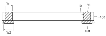
실시예에 따른 태양전지는 도 9에 도시된 바와 같이, 기판(100) 상에 형성된 후면전극 패턴(200), 광 흡수층(300), 버퍼층(400), 전면전극(500), 관통홀(10), 연결전극(50) 및 버스바(150)를 포함한다.As illustrated in FIG. 9, a solar cell according to an embodiment includes a back electrode pattern 200, a light absorbing layer 300, a buffer layer 400, a front electrode 500, and a through hole 10 formed on a substrate 100. ), A connection electrode 50 and a bus bar 150.
상기 관통홀(10)은 상기 기판(100)을 관통하여 형성되며, 상기 연결전극(50)은 상기 관통홀(10) 내부에 전도성 물질이 채워져 형성된다.The through hole 10 is formed through the substrate 100, and the connection electrode 50 is formed by filling a conductive material in the through hole 10.
상기 버스바(150)는 상기 기판(100)의 후면에 상기 연결전극(50)과 접촉하여 전기적으로 연결된다.The bus bar 150 is electrically connected to the rear surface of the substrate 100 in contact with the connection electrode 50.
상기 연결전극(50)이 상기 후면전극 패턴(200)과 접촉하여 전기적으로 연결되어, 상기 후면전극 패턴(200)과 상기 버스바(150)는 전기적으로 연결된다.The connection electrode 50 is electrically connected to the back electrode pattern 200 so that the back electrode pattern 200 and the bus bar 150 are electrically connected to each other.
이때, 상기 버스바(150)는 상기 기판(100)의 최외각에 형성된 상기 후면전극 패턴(200)과 전기적으로 연결된다.In this case, the bus bar 150 is electrically connected to the back electrode pattern 200 formed at the outermost portion of the substrate 100.
이하, 태양전지 제조공정에 따라 상기 태양전지를 더 자세히 설명하도록 한다.Hereinafter, the solar cell will be described in more detail according to the solar cell manufacturing process.
도 1 내지 도 11은 실시예에 따른 태양전지의 제조방법을 도시한 평면도 및 단면도이다.1 to 11 are plan and cross-sectional views illustrating a method of manufacturing a solar cell according to an embodiment.
우선, 도 1 및 도 2에 도시된 바와 같이, 기판(100)을 관통하는 관통홀(10)을 형성한다.First, as shown in FIGS. 1 and 2, a through hole 10 penetrating the substrate 100 is formed.
상기 기판(100)은 유리(glass)가 사용되고 있으며, 알루미나와 같은 세라믹 기판, 스테인레스 스틸, 티타늄기판 또는 폴리머 기판 등도 사용될 수 있다.The substrate 100 may be glass, and a ceramic substrate such as alumina, stainless steel, a titanium substrate, or a polymer substrate may also be used.
유리 기판으로는 소다라임 유리(sodalime glass)를 사용할 수 있으며, 폴리머 기판으로는 폴리이미드(polyimide)를 사용할 수 있다.Soda lime glass may be used as the glass substrate, and polyimide may be used as the polymer substrate.
또한, 상기 기판(100)은 리지드(rigid)하거나 플렉서블(flexible)할 수 있다.In addition, the substrate 100 may be rigid or flexible.
상기 관통홀(10)은 이후 형성될 버스바 및 후면전극 패턴의 모양에 따라 그 모양이 변형될 수 있으나, 실시예에서는 일 방향으로 길게 형성된 상기 관통홀(10)을 형성한다.The through hole 10 may be deformed according to the shape of the bus bar and the rear electrode pattern to be formed later, but in the embodiment, the through hole 10 is formed to be elongated in one direction.
도 2는 도 1의 I-I'의 단면도를 도시한 것이다.FIG. 2 illustrates a cross-sectional view of II ′ of FIG. 1.
상기 기판(100)의 양 가장자리에 두 개의 상기 관통홀(10)이 형성된다.Two through holes 10 are formed at both edges of the substrate 100.
이때, 한쪽 관통홀은 이후, (+)전극과 연결될 버스바와 연결되며, 또 다른 관통홀은 이후 (-)전극과 연결될 버스바와 연결되기 때문에 두 개가 형성된다.At this time, one through hole is then connected to the bus bar to be connected to the (+) electrode, and the other through hole is connected to the bus bar to be connected to the (-) electrode afterwards, and two are formed.
그러나, 상기 관통홀(10)의 갯수는 이에 한정되지 않고, 태양전지 셀의 구조에 따라 갯수가 변경될 수 있다.However, the number of the through holes 10 is not limited thereto, and the number may be changed according to the structure of the solar cell.
상기 관통홀(10)의 폭(W1)은 0.5mm~3mm의 크기로 형성될 수 있으며, 바람직하게는 1mm~2mm로 형성될 수 있다.The width W1 of the through hole 10 may be formed to a size of 0.5mm ~ 3mm, preferably 1mm ~ 2mm.
이어서, 도 3에 도시된 바와 같이, 상기 관통홀(10)의 내부를 채우는 연결전극(50)을 형성한다.Subsequently, as shown in FIG. 3, a connection electrode 50 filling the inside of the through hole 10 is formed.
상기 연결전극(50)은 상기 관통홀(10)이 채워지도록 Ag 또는 Al 페이스트(paste)를 삽입하여 형성될 수 있으며, 또한, 후면전극 물질인 몰리브덴(Mo)을 상기 관통홀(10)에 삽입되도록 형성할 수 있다.The connection electrode 50 may be formed by inserting Ag or Al paste to fill the through hole 10, and inserting molybdenum (Mo), which is a back electrode material, into the through hole 10. It may be formed to.
그러나, 상기 연결전극(50)을 형성하는 물질은 이에 한정되지 않고, 전도성 물질로 형성될 수 있다.However, the material forming the connection electrode 50 is not limited thereto, and may be formed of a conductive material.
그리고, 도 4에 도시된 바와 같이, 상기 기판(100)의 후면에 버스바(150)를 형성한다.And, as shown in Figure 4, to form a bus bar 150 on the back of the substrate 100.
상기 버스바(150)는 상기 기판(100)의 후면에 노출되도록 형성될 수 있으며, 상기 연결전극(50)과는 접촉하여 전기적으로 연결될 수 있다.The bus bar 150 may be formed to be exposed to the rear surface of the substrate 100, and may be electrically connected to the connection electrode 50.
상기 버스바(150)는 Al, Cu를 포함하는 도전성 물질로 형성될 수 있다.The bus bar 150 may be formed of a conductive material including Al and Cu.
상기 버스바(150)는 1mm~5mm의 폭(W2)으로 형성될 수 있으며, 바람직하게는 3mm~4mm로 형성될 수 있다.The bus bar 150 may be formed to have a width W2 of 1 mm to 5 mm, preferably 3 mm to 4 mm.
그리고, 상기 버스바(150)는 상기 연결전극(50)의 폭(W1)보다 넓게 형성될 수 있다.The bus bar 150 may be wider than the width W1 of the connection electrode 50.
이때, 상기 연결전극(50)과 버스바(150)의 형성 순서는 바뀔 수도 있다. 즉, 실시예에서는 연결전극(50)을 형성한 후, 상기 버스바(150)를 형성하였지만, 상기 버스바(150)를 먼저 형성한 후, 상기 연결전극(50)을 형성할 수도 있다.In this case, the forming order of the connection electrode 50 and the bus bar 150 may be changed. That is, although the bus bar 150 is formed after the connection electrode 50 is formed in the embodiment, the bus bar 150 may be formed first, and then the connection electrode 50 may be formed.
이어서, 도 5에 도시된 바와 같이, 상기 기판(100)의 전면에 후면전극 패턴(200)을 형성한다.Subsequently, as shown in FIG. 5, the back electrode pattern 200 is formed on the front surface of the substrate 100.
상기 후면전극 패턴(200)은 금속 등의 도전체로 형성될 수 있다.The back electrode pattern 200 may be formed of a conductor such as metal.
예를 들어, 상기 후면전극 패턴(200)은 몰리브덴(Mo) 타겟을 사용하여, 스퍼터링(sputtering) 공정에 의해 형성될 수 있다. For example, the back electrode pattern 200 may be formed by a sputtering process using a molybdenum (Mo) target.
이는, 몰리브덴(Mo)이 가진 높은 전기전도도, 광 흡수층과의 오믹(ohmic) 접합, Se 분위기 하에서의 고온 안정성 때문이다.This is because of high electrical conductivity of molybdenum (Mo), ohmic bonding with the light absorbing layer, and high temperature stability under Se atmosphere.
상기 후면전극 패턴(200)은 상기 관통홀(10)을 덮도록 형성될 수 있다. 즉, 상기 연결전극(50)과 접촉하여 전기적으로 연결될 수 있다.The back electrode pattern 200 may be formed to cover the through hole 10. That is, it may be electrically connected to the connection electrode 50.
즉, 상기 연결전극(50)으로 인해 상기 후면전극 패턴(200)과 버스바(150)는 전기적으로 연결된다.That is, the back electrode pattern 200 and the bus bar 150 are electrically connected by the connection electrode 50.
이때, 상기 관통홀(10)이 상기 기판(100)의 가장자리에 형성되어, 상기 기판(100)의 최외각에 형성된 상기 후면전극 패턴(200)과 상기 버스바(150)가 전기적으로 연결된다.In this case, the through hole 10 is formed at an edge of the substrate 100, and the back electrode pattern 200 and the bus bar 150 formed at the outermost portion of the substrate 100 are electrically connected to each other.
또한, 도면에는 도시하지 않았지만, 상기 후면전극 패턴(200)은 적어도 하나 이상의 층으로 형성될 수 있다.In addition, although not shown, the back electrode pattern 200 may be formed of at least one layer.
상기 후면전극 패턴(200)이 복수개의 층으로 형성될 때, 상기 후면전극 패턴(200)을 이루는 층들은 서로 다른 물질로 형성될 수 있다.When the back electrode pattern 200 is formed of a plurality of layers, the layers constituting the back electrode pattern 200 may be formed of different materials.
상기 후면전극 패턴(200) 사이로는 상기 기판(100)의 일부가 노출될 수 있다.A portion of the substrate 100 may be exposed between the rear electrode patterns 200.
또한, 상기 후면전극 패턴(200)은 스트라이프(stripe) 형태 또는 매트릭스(matrix) 형태로 배치될 수 있으며, 각각의 셀에 대응할 수 있다.In addition, the back electrode pattern 200 may be arranged in a stripe form or a matrix form and may correspond to each cell.
그러나, 상기 후면전극 패턴(200)은 상기의 형태에 한정되지 않고, 다양한 형태로 형성될 수 있다.However, the back electrode pattern 200 is not limited to the above form and may be formed in various forms.
실시예에서는 상기 연결전극(50) 및 버스바(150)를 형성한 후, 상기 후면전극 패턴(200)을 형성하여 상기 후면전극 패턴(200)과 버스바(150)를 전기적으로 연결시켰지만, 이에 한정되지 않고, 상기 기판(150)의 후면에 버스바(150)만 형성한 후, 상기 후면전극 패턴(200)을 형성할 수도 있다.In the embodiment, after the connection electrode 50 and the bus bar 150 are formed, the back electrode pattern 200 is formed to electrically connect the back electrode pattern 200 and the bus bar 150. The rear electrode pattern 200 may be formed after the bus bar 150 is formed on the rear surface of the substrate 150.
즉, 상기 연결전극(50)을 형성하지 않고, 상기 버스바(150)만 형성한 후, 상기 후면전극 패턴(200) 형성시, 상기 후면전극 패턴(200)의 물질이 상기 관통홀(10) 내부에 삽입되어, 상기 버스바(150)와 전기적으로 연결될 수도 있다.That is, after forming only the bus bar 150 without forming the connection electrode 50, when the back electrode pattern 200 is formed, a material of the back electrode pattern 200 is formed in the through hole 10. Inserted therein, it may be electrically connected to the bus bar 150.
그리고, 도 6에 도시된 바와 같이, 상기 후면전극 패턴(200) 상에 광 흡수층(300), 버퍼층(400)을 형성한다.6, a light absorbing layer 300 and a buffer layer 400 are formed on the back electrode pattern 200.
상기 광 흡수층(300)은 Ⅰb-Ⅲb-Ⅵb계 화합물을 포함한다. The light absorbing layer 300 includes an Ib-IIIb-VIb-based compound.
더 자세하게, 상기 광 흡수층(300)은 구리-인듐-갈륨-셀레나이드계(Cu(In, Ga)Se2, CIGS계) 화합물을 포함한다.In more detail, the light absorbing layer 300 includes a copper-indium-gallium-selenide-based (Cu (In, Ga) Se 2 , CIGS-based) compound.
이와는 다르게, 상기 광 흡수층(300)은 구리-인듐-셀레나이드계(CuInSe2, CIS계) 화합물 또는 구리-갈륨-셀레나이드계(CuGaSe2, CIS계) 화합물을 포함할 수 있다.Alternatively, the light absorbing layer 300 may include a copper-indium selenide-based (CuInSe 2 , CIS-based) compound or a copper-gallium-selenide-based (CuGaSe 2 , CIS-based) compound.
예를 들어, 상기 광 흡수층(300)을 형성하기 위해서, 구리 타겟, 인듐 타겟 및 갈륨 타겟을 사용하여, 상기 후면전극 패턴(200) 상에 CIG계 금속 프리커서(precursor)막이 형성된다. For example, to form the light absorbing layer 300, a CIG-based metal precursor film is formed on the back electrode pattern 200 using a copper target, an indium target, and a gallium target.
이후, 상기 금속 프리커서막은 셀레니제이션(selenization) 공정에 의해서, 셀레늄(Se)과 반응하여 CIGS계 광 흡수층(300)이 형성된다.Subsequently, the metal precursor film is reacted with selenium (Se) by a selenization process to form a CIGS-based light absorbing layer 300.
또한, 상기 금속 프리커서막을 형성하는 공정 및 셀레니제이션 공정 동안에, 상기 기판(100)에 포함된 알칼리(alkali) 성분이 상기 후면전극 패턴(200)을 통해서, 상기 금속 프리커서막 및 상기 광 흡수층(300)에 확산된다.In addition, during the process of forming the metal precursor film and the selenization process, an alkali component included in the substrate 100 may pass through the back electrode pattern 200, and the metal precursor film and the light absorbing layer ( 300).
알칼리(alkali) 성분은 상기 광 흡수층(300)의 그레인(grain) 크기를 향상시키고, 결정성을 향상시킬 수 있다.An alkali component may improve grain size and improve crystallinity of the light absorbing layer 300.
또한, 상기 광 흡수층(300)은 구리,인듐,갈륨,셀레나이드(Cu, In, Ga, Se)를 동시증착법(co-evaporation)에 의해 형성할 수도 있다.In addition, the light absorbing layer 300 may form copper, indium, gallium, selenide (Cu, In, Ga, Se) by co-evaporation.
상기 광 흡수층(300)은 상기 후면전극 패턴(200) 상에 형성되며, 상기 후면전극 패턴(200) 사이로 일부가 노출된 상기 기판(100) 상에 형성될 수 있다.The light absorbing layer 300 may be formed on the back electrode pattern 200, and may be formed on the substrate 100 partially exposed between the back electrode patterns 200.
상기 광 흡수층(300)은 외부의 광을 입사받아, 전기 에너지로 변환시킨다. 상기 광 흡수층(300)은 광전효과에 의해서 광 기전력을 생성한다.The light absorbing layer 300 receives external light and converts the light into electrical energy. The light absorbing layer 300 generates photo electromotive force by the photoelectric effect.
상기 버퍼층(400)은 상기 광 흡수층(300) 상에 형성되고, 적어도 하나 이상의 층으로 형성되며, 상기 광 흡수층(300)이 형성된 상기 기판(100) 상에 황화 카드뮴(CdS), ITO, ZnO, i-ZnO 중 어느 하나 또는 이들의 적층으로 형성될 수 있다.The buffer layer 400 is formed on the light absorbing layer 300, is formed of at least one or more layers, and cadmium sulfide (CdS), ITO, ZnO, on the substrate 100 on which the light absorbing layer 300 is formed. It may be formed of any one of i-ZnO or a stack thereof.
이때, 상기 버퍼층(400)은 n형 반도체 층이고, 상기 광 흡수층(300)은 p형 반도체 층이다. 따라서, 상기 광 흡수층(300) 및 버퍼층(400)은 pn 접합을 형성한다.In this case, the buffer layer 400 is an n-type semiconductor layer, the light absorbing layer 300 is a p-type semiconductor layer. Thus, the light absorbing layer 300 and the buffer layer 400 form a pn junction.
상기 버퍼층(400)은 상기 광 흡수층(300)과 이후 형성될 전면전극의 사이에 배치된다.The buffer layer 400 is disposed between the light absorbing layer 300 and the front electrode to be formed later.
즉, 상기 광 흡수층(300)과 전면전극은 격자상수와 에너지 밴드 갭의 차이가 크기 때문에, 밴드갭이 두 물질의 중간에 위치하는 상기 버퍼층(400)을 삽입하여 양호한 접합을 형성할 수 있다.That is, since the difference between the lattice constant and the energy band gap is large between the light absorbing layer 300 and the front electrode, a good junction may be formed by inserting the buffer layer 400 having a band gap between the two materials.
본 실시예에서는 한 개의 버퍼층을 상기 광 흡수층(300) 상에 형성하였지만, 이에 한정되지 않고, 상기 버퍼층은 복수개의 층으로 형성될 수도 있다.In the present exemplary embodiment, one buffer layer is formed on the light absorbing layer 300, but the present invention is not limited thereto, and the buffer layer may be formed of a plurality of layers.
이어서, 도 7에 도시된 바와 같이, 상기 광 흡수층(300) 및 버퍼층(400)을 관통하는 콘택패턴(310)을 형성한다.Subsequently, as shown in FIG. 7, a contact pattern 310 penetrating the light absorbing layer 300 and the buffer layer 400 is formed.
상기 콘택패턴(310)은 기계적인(mechnical) 방법으로 형성할 수 있으며, 상기 후면전극 패턴(200)의 일부가 노출된다. 상기 콘택패턴(310)은 상기 후면전극 패턴(200)과 인접한 영역에 형성될 수 있다.The contact pattern 310 may be formed by a mechanical method, and a portion of the back electrode pattern 200 is exposed. The contact pattern 310 may be formed in an area adjacent to the back electrode pattern 200.
그리고, 도 8에 도시된 바와 같이, 상기 버퍼층(400) 상에 투명한 도전물질을 적층하여 전면전극(500) 및 접속배선(700)을 형성한다.8, a transparent conductive material is stacked on the buffer layer 400 to form the front electrode 500 and the connection wiring 700.
상기 투명한 도전물질을 상기 버퍼층(400) 상에 적층시킬 때, 상기 투명한 도전물질이 상기 콘택패턴(310)의 내부에도 삽입되어, 상기 접속배선(700)을 형성할 수 있다. 즉, 상기 전면전극(500) 및 접속배선(700)은 동일한 물질로 형성될 수 있다.When the transparent conductive material is stacked on the buffer layer 400, the transparent conductive material may also be inserted into the contact pattern 310 to form the connection wiring 700. That is, the front electrode 500 and the connection wiring 700 may be formed of the same material.
상기 후면전극 패턴(200)과 전면전극(500)은 상기 접속배선(700)에 의해 전기적으로 연결된다.The back electrode pattern 200 and the front electrode 500 are electrically connected to each other by the connection wiring 700.
상기 전면전극(500)은 상기 기판(100) 상에 스퍼터링 공정을 진행하여 알루미늄으로 도핑된 산화 아연으로 형성된다.The front electrode 500 is formed of zinc oxide doped with aluminum by performing a sputtering process on the substrate 100.
상기 전면전극(500)은 상기 광 흡수층(300)과 pn접합을 형성하는 윈도우(window)층으로서, 태양전지 전면의 투명전극의 기능을 하기 때문에 광투과율이 높고 전기 전도성이 좋은 산화 아연(ZnO)으로 형성된다.The front electrode 500 is a window layer forming a pn junction with the light absorbing layer 300. Since the front electrode 500 functions as a transparent electrode on the front of the solar cell, zinc oxide (ZnO) having high light transmittance and good electrical conductivity is provided. Is formed.
이때, 상기 산화 아연에 알루미늄를 도핑함으로써 낮은 저항값을 갖는 전극을 형성할 수 있다.At this time, the aluminum oxide may be doped with aluminum to form an electrode having a low resistance value.
상기 전면전극(500)인 산화 아연 박막은 RF 스퍼터링방법으로 ZnO 타겟을 사용하여 증착하는 방법과 Zn 타겟을 이용한 반응성 스퍼터링, 그리고 유기금속화학증착법 등으로 형성될 수 있다.The zinc oxide thin film as the front electrode 500 may be formed by a method of depositing using a ZnO target by RF sputtering, reactive sputtering using a Zn target, and an organometallic chemical vapor deposition method.
또한, 전기광학적 특성이 뛰어난 ITO(Indium tin Oxide) 박막을 산화 아연 박막 상에 층착한 2중 구조를 형성할 수도 있다.In addition, a double structure in which an indium tin oxide (ITO) thin film having excellent electro-optical properties is laminated on a zinc oxide thin film may be formed.
이어서, 도 9에 도시된 바와 같이, 상기 광 흡수층(300), 버퍼층(400) 및 전면전극(500)을 관통하는 분리패턴(320)을 형성한다.Subsequently, as illustrated in FIG. 9, a separation pattern 320 penetrating the light absorbing layer 300, the buffer layer 400, and the front electrode 500 is formed.
상기 분리패턴(320)은 기계적인(mechnical) 방법으로 형성할 수 있으며, 상기 후면전극 패턴(200)의 상면의 일부가 노출된다.The separation pattern 320 may be formed by a mechanical method, and a part of the top surface of the back electrode pattern 200 is exposed.
상기 버퍼층(400) 및 전면전극(500)은 상기 분리패턴(320)에 의해 구분될 수 있으며, 상기 분리패턴(320)에 의해 각각의 셀(C1, C2)은 서로 분리될 수 있다.The buffer layer 400 and the front electrode 500 may be separated by the separation pattern 320, and the cells C1 and C2 may be separated from each other by the separation pattern 320.
상기 분리패턴(320)에 의해 상기 전면전극(500), 버퍼층(400) 및 광 흡수층(300)은 스트라이프 형태 또는 매트릭스 형태로 배치될 수 있다.The front electrode 500, the buffer layer 400, and the light absorbing layer 300 may be arranged in the form of a stripe or a matrix by the separation pattern 320.
상기 분리패턴(320)은 상기의 형태에 한정되지 않고, 다양한 형태로 형성될 수 있다.The separation pattern 320 is not limited to the above form and may be formed in various forms.
상기 분리패턴(320)에 의해 상기 후면전극 패턴(200), 광 흡수층(300), 버퍼층(400) 및 전면전극(500)을 포함하는 셀(C1, C2)이 형성된다.Cells C1 and C2 including the back electrode pattern 200, the light absorbing layer 300, the buffer layer 400, and the front electrode 500 are formed by the separation pattern 320.
이때, 상기 접속배선(700)에 의해 각각의 셀(C1, C2)은 서로 연결될 수 있다. 즉, 상기 접속배선(700)은 제2셀(C2)의 후면전극 패턴(200)과 상기 제2셀(C2)에 인접하는 상기 제1셀(C1)의 전면전극(500)을 전기적으로 연결한다.In this case, each of the cells C1 and C2 may be connected to each other by the connection wiring 700. That is, the connection wiring 700 electrically connects the back electrode pattern 200 of the second cell C2 and the front electrode 500 of the first cell C1 adjacent to the second cell C2. do.
도 10은 상기 분리패턴(320)에 의해 태양전지 셀이 형성된 상기 기판(100)의 전면을 도시한 평면도이며, 도 11은 상기 버스바(150)가 형성된 상기 기판(100)의 후면을 도시한 평면도이다.FIG. 10 is a plan view illustrating a front surface of the substrate 100 on which a solar cell is formed by the separation pattern 320, and FIG. 11 illustrates a rear surface of the substrate 100 on which the bus bar 150 is formed. Top view.
상기 버스바(150)가 상기 기판(100)의 후면에 형성되기 때문에, 상기 전면전극(500) 상으로 버스바를 형성하여, 상기 버스바의 신호를 상기 기판(100)의 후면으로 전달하기 위한 전극을 추가적으로 형성할 필요가 없다.Since the bus bar 150 is formed on the rear surface of the substrate 100, a bus bar is formed on the front electrode 500 to transmit a signal of the bus bar to the rear surface of the substrate 100. It is not necessary to form additionally.
또한, 상기 후면전극 패턴(200)과 직접 연결된 상기 연결전극(50)의 폭(W1)이 상기 버스바(150)의 폭(W2)보다 좁게 형성되어, 태양전지 셀 형성 영역을 넓힐 수 있다.In addition, the width W1 of the connection electrode 50 directly connected to the back electrode pattern 200 is formed to be narrower than the width W2 of the bus bar 150, thereby widening the solar cell forming region.
즉, 기존에 형성된 버스바는 상기 전면전극(500) 상으로 형성되어, 상기 버스바의 폭만큼 태양전지 셀 형성 영역이 좁아졌지만, 본 실시예에서는 상기 버스바(150)보다 폭이 좁은 상기 연결전극(50)이 상기 후면전극 패턴(200)과 연결되므로, 태양전지 셀 형성 영역이 넓어질 수 있다.That is, the existing bus bar is formed on the front electrode 500, the solar cell forming region is narrowed by the width of the bus bar, in the present embodiment, the connection narrower than the bus bar 150 Since the electrode 50 is connected to the back electrode pattern 200, the solar cell formation region may be widened.
이에, 태양전지 셀 형성 영역이 넓어짐에 따라, 태양전지의 효율도 증가될 수 있다.Thus, as the solar cell forming region is widened, the efficiency of the solar cell may also be increased.
이상에서 설명한 실시예에 따른 태양전지 및 이의 제조방법은 버스바보다 폭이 좁은 연결전극이 관통홀을 통해 후면전극 패턴과 연결되어, 태양전지 셀 형성 영역이 넓어져, 태양전지의 효율이 증대될 수 있다.In the solar cell and the method of manufacturing the same according to the embodiments described above, a connection electrode having a narrower width than the bus bar is connected to the rear electrode pattern through the through hole, so that the solar cell forming region is widened, thereby increasing the efficiency of the solar cell. Can be.
이상에서 실시예를 중심으로 설명하였으나 이는 단지 예시일 뿐 본 발명을 한정하는 것이 아니며, 본 발명이 속하는 분야의 통상의 지식을 가진 자라면 본 실시예의 본질적인 특성을 벗어나지 않는 범위에서 이상에 예시되지 않은 여러 가지의 변형과 응용이 가능함을 알 수 있을 것이다. 예를 들어, 실시예에 구체적으로 나타난 각 구성 요소는 변형하여 실시할 수 있는 것이다. 그리고 이러한 변형과 응용에 관계된 차이점들은 첨부된 청구 범위에서 규정하는 본 발명의 범위에 포함되는 것으로 해석되어야 할 것이다.Although the above description has been made based on the embodiments, these are merely examples and are not intended to limit the present invention. Those skilled in the art to which the present invention pertains may not have been exemplified above without departing from the essential characteristics of the present embodiments. It will be appreciated that many variations and applications are possible. For example, each component specifically shown in the embodiment can be modified. And differences relating to such modifications and applications will have to be construed as being included in the scope of the invention defined in the appended claims.