WO2011013760A1 - Photoelectric element - Google Patents
Photoelectric element Download PDFInfo
- Publication number
- WO2011013760A1 WO2011013760A1 PCT/JP2010/062823 JP2010062823W WO2011013760A1 WO 2011013760 A1 WO2011013760 A1 WO 2011013760A1 JP 2010062823 W JP2010062823 W JP 2010062823W WO 2011013760 A1 WO2011013760 A1 WO 2011013760A1
- Authority
- WO
- WIPO (PCT)
- Prior art keywords
- transport layer
- organic compound
- hole transport
- redox
- gel
- Prior art date
Links
Images
Classifications
-
- H—ELECTRICITY
- H01—ELECTRIC ELEMENTS
- H01G—CAPACITORS; CAPACITORS, RECTIFIERS, DETECTORS, SWITCHING DEVICES OR LIGHT-SENSITIVE DEVICES, OF THE ELECTROLYTIC TYPE
- H01G9/00—Electrolytic capacitors, rectifiers, detectors, switching devices, light-sensitive or temperature-sensitive devices; Processes of their manufacture
- H01G9/20—Light-sensitive devices
- H01G9/2059—Light-sensitive devices comprising an organic dye as the active light absorbing material, e.g. adsorbed on an electrode or dissolved in solution
-
- H—ELECTRICITY
- H10—SEMICONDUCTOR DEVICES; ELECTRIC SOLID-STATE DEVICES NOT OTHERWISE PROVIDED FOR
- H10K—ORGANIC ELECTRIC SOLID-STATE DEVICES
- H10K50/00—Organic light-emitting devices
- H10K50/10—OLEDs or polymer light-emitting diodes [PLED]
- H10K50/11—OLEDs or polymer light-emitting diodes [PLED] characterised by the electroluminescent [EL] layers
- H10K50/135—OLEDs or polymer light-emitting diodes [PLED] characterised by the electroluminescent [EL] layers comprising mobile ions
-
- H—ELECTRICITY
- H10—SEMICONDUCTOR DEVICES; ELECTRIC SOLID-STATE DEVICES NOT OTHERWISE PROVIDED FOR
- H10K—ORGANIC ELECTRIC SOLID-STATE DEVICES
- H10K50/00—Organic light-emitting devices
- H10K50/10—OLEDs or polymer light-emitting diodes [PLED]
- H10K50/14—Carrier transporting layers
-
- H—ELECTRICITY
- H10—SEMICONDUCTOR DEVICES; ELECTRIC SOLID-STATE DEVICES NOT OTHERWISE PROVIDED FOR
- H10K—ORGANIC ELECTRIC SOLID-STATE DEVICES
- H10K85/00—Organic materials used in the body or electrodes of devices covered by this subclass
- H10K85/60—Organic compounds having low molecular weight
- H10K85/649—Aromatic compounds comprising a hetero atom
- H10K85/657—Polycyclic condensed heteroaromatic hydrocarbons
- H10K85/6572—Polycyclic condensed heteroaromatic hydrocarbons comprising only nitrogen in the heteroaromatic polycondensed ring system, e.g. phenanthroline or carbazole
-
- Y—GENERAL TAGGING OF NEW TECHNOLOGICAL DEVELOPMENTS; GENERAL TAGGING OF CROSS-SECTIONAL TECHNOLOGIES SPANNING OVER SEVERAL SECTIONS OF THE IPC; TECHNICAL SUBJECTS COVERED BY FORMER USPC CROSS-REFERENCE ART COLLECTIONS [XRACs] AND DIGESTS
- Y02—TECHNOLOGIES OR APPLICATIONS FOR MITIGATION OR ADAPTATION AGAINST CLIMATE CHANGE
- Y02E—REDUCTION OF GREENHOUSE GAS [GHG] EMISSIONS, RELATED TO ENERGY GENERATION, TRANSMISSION OR DISTRIBUTION
- Y02E10/00—Energy generation through renewable energy sources
- Y02E10/50—Photovoltaic [PV] energy
- Y02E10/542—Dye sensitized solar cells
-
- Y—GENERAL TAGGING OF NEW TECHNOLOGICAL DEVELOPMENTS; GENERAL TAGGING OF CROSS-SECTIONAL TECHNOLOGIES SPANNING OVER SEVERAL SECTIONS OF THE IPC; TECHNICAL SUBJECTS COVERED BY FORMER USPC CROSS-REFERENCE ART COLLECTIONS [XRACs] AND DIGESTS
- Y02—TECHNOLOGIES OR APPLICATIONS FOR MITIGATION OR ADAPTATION AGAINST CLIMATE CHANGE
- Y02E—REDUCTION OF GREENHOUSE GAS [GHG] EMISSIONS, RELATED TO ENERGY GENERATION, TRANSMISSION OR DISTRIBUTION
- Y02E10/00—Energy generation through renewable energy sources
- Y02E10/50—Photovoltaic [PV] energy
- Y02E10/549—Organic PV cells
Definitions
- the present invention relates to a photoelectric element that converts light into electricity or converts electricity into light.
- photoelectric elements have been used for photoelectric conversion elements such as photovoltaic cells and solar cells, light emitting elements such as organic EL, optical display elements such as electrochromic display elements and electronic paper, and sensor elements that sense temperature and light. It is used.
- This interface is an interface between the hole transport layer and a layer other than the hole transport layer, and refers to an interface in which holes are generated by external energy and holes are injected from the outside.
- This hole transport layer has been conventionally formed from a metal, an organic semiconductor, an inorganic semiconductor, a conductive polymer, conductive carbon, or the like.
- a hole transport layer for transporting holes is formed from an organic substance such as poly (3-hexylthiophene), triphenyldiamine (monomer, polymer, etc.), polyaniline, polypyrrole, polythiophene, or a phthalocyanine compound.
- organic substance such as poly (3-hexylthiophene), triphenyldiamine (monomer, polymer, etc.), polyaniline, polypyrrole, polythiophene, or a phthalocyanine compound.
- the conversion efficiency of photoelectric conversion elements is being improved by the hole transport ability of these organic substances (see Patent Documents 1 to 3).
- a thin film may be formed on a substrate of a structure obtained by chemically bonding an electron donating molecule (donor) and an electron accepting molecule (acceptor). It has been reported (see Non-Patent Document 1).
- the present invention has been made in view of the above points, and has an object to provide a photoelectric device having a hole transport layer having excellent hole transport characteristics and a sufficiently wide reaction interface, and having excellent conversion efficiency. To do.
- the photoelectric element according to the present invention includes a pair of electrodes, an electron transport layer and a hole transport layer sandwiched between the electrodes, and an electrolyte solution, and the hole transport layer can be repeatedly oxidized and reduced.
- a first organic compound having a redox part is provided, the electrolyte solution stabilizes the reduction state of the redox part, and the organic compound and the electrolyte solution constitute a first gel layer.
- the photoelectric element according to the present invention may include a sensitizing dye present in the first gel layer.
- the hole transport layer may contain a nitroxy radical polymer.
- the electron transport layer may contain at least one compound selected from the group consisting of a viologen derivative, a phenoxyl derivative, and a quinone derivative.
- the open-circuit voltage A (V) of the photoelectric element according to the present invention when the light of 200 lux is irradiated for 5 minutes and the open-circuit voltage B (5 minutes after the light is shielded at this time) V) may satisfy the following relational expression. (B / A) ⁇ 100 ⁇ 10
- the electron transport layer includes a second organic compound having a redox portion capable of repeated redox, and the second organic compound and the electrolyte solution are the second gel layer.
- the redox potential of the electron transport layer may be more noble than the redox potential of the hole transport layer.
- the photoelectric element according to the present invention may include a sensitizing dye that performs an electron transfer reaction with one or both of the electron transport layer and the hole transport layer.
- the hole transport property of the hole transport layer is improved, the reaction interface is widened, and the conversion efficiency of the photoelectric element is improved.
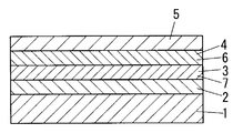
- the photoelectric element is formed by sandwiching the electron transport layer 3 and the hole transport layer 4 between the pair of electrodes 2 and 5.
- the hole transport layer 4 includes an organic compound having a redox portion capable of repeated redox.
- the organic compound is formed as a gel layer 6 including an electrolyte solution that stabilizes the oxidation state of the redox portion, and a sensitizing dye is present in the gel layer 6.
- the organic compound of the hole transport layer 4 and the electrolyte solution constitute the gel layer 6, thereby increasing the reaction interface of the organic compound and improving the conversion efficiency.
- the organic compound of the hole transport layer 4 and the electrolyte solution constitute the gel layer 6 and the sensitizing dye is present in the gel layer 6, thereby increasing the reaction interface of the organic compound and converting The efficiency is improved, and the hole transfer efficiency from the sensitizing dye to the organic compound of the hole transport layer 4 is improved, thereby improving the hole transport efficiency.
- the hole transport layer 4 preferably contains a nitroxy radical polymer.
- the nitroxy radical site expresses a high-speed hole transporting function, has stability as an oxidation state, and has a polymerized structure. This brings about the effect of expressing the transport function.
- the electron transport layer 3 preferably contains at least one compound selected from the group consisting of a viologen derivative, a phenoxyl derivative, an imide derivative, and a quinone derivative.
- the electron transport layer 3 has stability as an organic compound and exhibits high electron transport properties, and exhibits an effective function as the electron transport layer 3.
- the photoelectric device has an open circuit voltage A (V) at the time when 200 lux light is irradiated for 5 minutes, and an open circuit voltage B at the time when 5 minutes have passed since the light was shielded at this time.
- V preferably satisfies the following relational expression.
- B / A ⁇ 100 ⁇ 10
- the photoelectric element according to the present embodiment may be configured as follows.
- This photoelectric element is formed by sandwiching an electron transport layer 3 and a hole transport layer 4 between a pair of electrodes 2 and 5.
- the electron transport layer 3 is formed by including an organic compound having a redox portion capable of repeated redox.
- the organic compound is formed as a gel layer 6 including an electrolyte solution that stabilizes the redox state of the redox portion.
- the hole transport layer 4 is formed by including an organic compound having a redox portion that can be repeatedly redox.
- the organic compound is formed as a gel layer 7 including an electrolyte solution that stabilizes the redox state of the redox portion.
- the electron transport layer 3 has a noble oxidation-reduction potential with respect to the hole transport layer 4.
- a configuration is provided in which one or both of the electron transport layer 3 and the hole transport layer 4 is provided with a sensitizing dye that performs an electron transfer reaction.
- the electron transport layer 3 and the hole transport layer 4 as the gel layers 6 and 7, it becomes possible to provide a photoelectric element free from the problem of electrolyte leakage.
- the electron transport layer 3 and the hole transport layer 4 as the gel layers 6 and 7 and allowing one or both of the electron transport layer 3 and the hole transport layer 4 to interact with the sensitizing dye, It is possible to provide a photoelectric element having a wide reaction interface and excellent conversion efficiency. Thereby, there can be provided a high-output photoelectric device and a dye-sensitized solar cell free from liquid leakage.
- the photoelectric element is formed by sandwiching an electron transport layer 3 and a hole transport layer 4 between a pair of electrodes 2 and 5. That is, the photoelectric element includes a first electrode 2, a second electrode 5, and an electron transport layer 3 and a hole transport layer 4 sandwiched between the first electrode 2 and the second electrode 5.
- the photoelectric element includes a first electrode 2, a second electrode 5, and an electron transport layer 3 and a hole transport layer 4 sandwiched between the first electrode 2 and the second electrode 5.
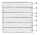
- the bases 1 and 8 are provided outside the electrodes 2 and 5, respectively. That is, the first substrate 1 is provided on the first electrode 2, and the second substrate 8 is provided on the second electrode 5.
- the hole transport layer 4 is formed from an organic compound having a redox portion (first organic compound).
- the first organic compound swells with the electrolyte solution to form the gel layer 6 (first gel layer 6). That is, the first organic compound having an oxidation-reduction portion and the electrolyte solution constitute the first gel layer 6, and the hole transport layer 4 is constituted by the first organic compound in the first gel layer 6. Sensitizing dye is present in the first gel layer 6.
- the photoelectric element includes the sensitizing dye as described above, but the photoelectric element may not include the sensitizing dye.
- the first electrode 2 is electrically connected to the electron transport layer 3.
- the first electrode 2 exhibits a function of extracting electrons from the electron transport layer 3 to the outside or injecting electrons into the electron transport layer 3.
- the first electrode 2 may also have a function of holding the electron transport layer 3.
- the second electrode 5 is electrically connected to the hole transport layer 4.
- the second electrode 5 exhibits a function of extracting electrons from the hole transport layer 4 to the outside or injecting holes into the hole transport layer 4.
- the external means a power supply circuit, a secondary battery, a capacitor, or the like that is electrically connected to the photoelectric element.
- the first electrode 2 may be formed from a single film of a conductive material such as a metal, but in this embodiment, a conductive material is formed on an insulating first base material 1 such as glass or a film. By laminating, the first electrode 2 is formed on the first substrate 1.
- the conductive material include metals such as platinum, gold, silver, copper, aluminum, rhodium, and indium; carbon; indium-tin composite oxide, tin oxide doped with antimony, and tin oxide doped with fluorine. Examples thereof include conductive metal oxides; composites of the above metals and compounds; materials obtained by coating the above metals and compounds with silicon oxide, tin oxide, titanium oxide, zirconium oxide, aluminum oxide, and the like.
- the surface resistance of the first electrode 2 is preferably as low as possible, but the surface resistance is preferably 200 ⁇ / ⁇ or less, more preferably 50 ⁇ / ⁇ or less.
- the lower limit of the surface resistance is not particularly limited, but is usually 0.1 ⁇ / ⁇ .
- the second electrode 5 may also be formed of a single film of a conductive material such as a metal, but in this embodiment, the conductive material is laminated on an insulating second base material 8 such as glass or film. Thus, the second electrode 5 is formed on the second substrate 8.
- the electrode material (conductive material) for forming the second electrode 5 depends on the type of element to be produced.
- metals such as platinum, gold, silver, copper, aluminum, rhodium, and indium, graphite, and carbon nanotubes
- Conductive metal oxides such as carbon materials such as carbon carrying platinum, indium-tin composite oxide, tin oxide doped with antimony, tin oxide doped with fluorine; composites of the above metals and compounds; And a material obtained by coating silicon oxide, tin oxide, titanium oxide, zirconium oxide, aluminum oxide or the like on a compound; conductive polymers such as polyethylenedioxythiophene, polypyrrole, polyaniline, and the like.
- the first electrode 2 or the second electrode 5 made of a transparent conductive oxide layer made of indium oxide, tin oxide, zinc oxide or the like on the first substrate 1 or the second substrate 8. Is formed on the light-transmitting first base material 1 or the second base material 8 made of, for example, glass or resin by a vacuum process such as sputtering or vapor deposition.
- the second electrode 5 may be formed, or the first electrode 2 or the second electrode 5 may be formed by a wet method such as spin coating, spraying, or screen printing.
- the photoelectric element is a power generation element, a light emitting element, an optical sensor, or the like.
- the light transmittance of the first substrate 1 or the second substrate 8 is high. Is desirable.
- the preferred light transmittance of the first substrate 1 or the second substrate 8 is 50% or more, more preferably 80% or more at a wavelength of 500 nm.
- the thicknesses of the first electrode 2 and the second electrode 5 are preferably in the range of 0.1 to 10 ⁇ m.
- the first electrode 2 and the second electrode 5 are formed with a uniform thickness, and a decrease in light transmittance of the first electrode 2 and the second electrode 5 is suppressed. Sufficient light enters the electron transport layer 3 and the hole transport layer 4 through the electrode 2 and the second electrode 5.
- the hole transport layer 4 refers to a layer having a function of receiving holes from a sensitizing dye and transporting them to an electrode in a light irradiation environment.
- a redox potential is applied to a silver / silver chloride reference electrode.
- it refers to a layer having an oxidation-reduction portion that is baser than +100 mV.
- the organic compound (first organic compound) constituting the hole transport layer 4 has a redox part that can be repeatedly redox as a part of its molecule, and swells including an electrolyte solution as another part. And has a portion (gel portion) that becomes a gel.
- the redox moiety is chemically bonded to the gel site.
- the positional relationship between the redox moiety and the gel part in the molecule of the first organic compound is not particularly limited. For example, when a skeleton such as the main chain of the molecule is formed by the gel part, the redox part is a side chain. As attached to the main chain.
- numerator of a 1st organic compound may have a structure where the molecular skeleton which forms a gel part, and the molecular skeleton which forms a redox part couple
- the redox part and the gel part are present in the same molecule of the first organic compound, the redox part is held by the first gel layer 6 at a position where holes are easily transported.
- redox redox reaction
- a redox moiety means a site that can stably send and receive electrons by a redox reaction. Is.
- the gel layer refers to a layer formed by swelling an organic compound having a redox moiety with an electrolyte solution. That is, in the gel state, the organic compound has a three-dimensional network structure, and the state where the liquid fills the network space is called a gel layer.
- the redox moiety capable of repeated redox refers to a site that reversibly becomes an oxidant and a reductant in a redox reaction.
- the redox moiety is preferably a redox-based constituent material in which the oxidant and the reductant have the same charge.
- the degree of swelling is a physical index that affects the size of the reaction interface in the first gel layer 6 and the second gel layer 7 described later.
- the swelling degree said here is represented by the following formula.
- a gel dry body refers to what is obtained by drying the 1st gel layer 6 or the 2nd gel layer 7.
- FIG. Drying the first gel layer 6 or the second gel layer 7 means removing the solution contained in the first gel layer 6 or the second gel layer 7, particularly removing the solvent.
- Examples of the method for drying the first gel layer 6 or the second gel layer 7 include a method for removing the solution or solvent from the first gel layer 6 or the second gel layer 7 in a heating and vacuum environment, and the like. And a method of removing the solution or the solvent contained in the first gel layer 6 or the second gel layer 7 with the above-mentioned solvent.
- the solution or solvent When removing the solution or solvent encapsulated in the first gel layer 6 or the second gel layer 7 with another solvent, the solution or solvent has high affinity with the encapsulated solution or solvent, and the heating or vacuum environment Selecting a solvent that is easy to remove among them provides an efficient removal effect of the solution or solvent contained in the first gel layer 6 or the second gel layer 7.
- the degree of swelling of the first gel layer 6 is preferably 110 to 3000%, and more preferably 150 to 500%.
- the degree of swelling is 110% or more, particularly 150% or more, the amount of the electrolyte component in the gel layer 6 is sufficiently increased and the degree of stabilization of the redox portion is increased, and the degree of swelling is 3000%.
- the density of the redox portion in the first gel layer 6 is sufficiently large because the amount is particularly 500% or less, and the hole transport layer 4 exhibits a very excellent hole transport capability. The characteristics of the photoelectric element are further improved.
- the first organic compound having a redox moiety and a gel part may be a low molecular weight substance or a high molecular weight substance.
- an organic compound that forms a so-called low-molecular gel via a hydrogen bond or the like can be used as the first organic compound.
- the first organic compound is a polymer, it is preferable that the first organic compound is an organic compound having a number average molecular weight of 1000 or more because the gelling function can be spontaneously expressed.
- the upper limit of the molecular weight of the first organic compound in the case of a polymer is not particularly limited, but is preferably 1,000,000 or less.
- the gel state of the first gel layer 6 is preferably, for example, konjac or an external shape such as an ion exchange membrane, but is not particularly limited.
- the redox moiety refers to a site that is reversibly converted into an oxidant and a reductant in a redox reaction.
- the redox moiety is preferably a redox-based constituent material in which the oxidant and the reductant have the same charge.
- the first organic compound having the oxidation-reduction part and the gel part as described above in one molecule is represented by the following general formula, for example.
- (X i ) nj : Y k (X i ) n and (X i ) nj represent a gel site, and X i represents a monomer of a compound that forms the gel site.
- the gel site can be composed of a polymer backbone.
- Y represents a redox moiety bonded to X.
- j and k are each an arbitrary integer representing the number of (X i ) n and Y contained in one molecule, and both are preferably in the range of 1 to 100,000.
- the redox moiety Y may be bonded to any part of the polymer skeleton constituting the gel part (X i ) n and (X i ) nj .
- the oxidation-reduction part Y may contain different types of materials (atomic groups). In this case, materials (atomic groups) having a close oxidation-reduction potential are preferable from the viewpoint of the electron exchange reaction.
- Examples of the first organic compound having the redox part and the gel part in one molecule and constituting the hole transport layer 4 include chemical species having unpaired electrons, that is, compounds having radicals (stable radical compounds). It is done.
- the stable radical compound a radical compound having nitroxide (NO.) In the molecule is preferable.
- the molecular weight (number average molecular weight) of the stable radical compound is preferably 1000 or more. In this case, since the stable radical compound becomes solid at room temperature or approaches the solid, it is difficult to volatilize and the stability of the device is improved. .
- a stable radical compound is a compound that generates a radical compound in at least one of an electrochemical oxidation reaction and an electrochemical reduction reaction.
- the kind of stable radical compound is not specifically limited, It is preferable that it is a stable radical compound.
- the stable radical compound is preferably an organic compound containing any one or both of the following [Chemical Formula 1] and [Chemical Formula 2] structural units.
- the substituent R 1 is a substituted or unsubstituted C2-C30 alkylene group, a C2-C30 alkenylene group, or a C4-C30 arylene group, and X is a nitroxyl radical group.
- X is a nitroxyl radical group.
- an oxy radical group, a sulfur radical group, a hydrazyl radical group, a carbon radical group, or a boron radical group is preferable.
- n 1 is an integer of 2 or more.
- the substituents R 2 and R 3 are each independently a substituted or unsubstituted C2-C30 alkylene group, a C2-C30 alkenylene group, or a C4-C30 arylene group, and Y is , A nitroxyl radical group, a sulfur radical group, a hydrazyl radical group, or a carbon radical group, and n 2 is an integer of 2 or more.
- Examples of the stable radical compound represented by [Chemical Formula 1] and Formula [Chemical Formula 2] include an oxy radical compound, a nitroxyl radical compound, a carbon radical compound, a nitrogen radical compound, a boron radical compound, and a sulfur radical compound.
- oxy radical compound examples include aryloxy radical compounds represented by the following [Chemical Formula 3] to [Chemical Formula 4], semiquinone radical compounds represented by [Chemical Formula 5], and the like.
- each of the substituents R 4 to R 7 is independently a hydrogen atom, a substituted or unsubstituted aliphatic or aromatic C1-C30 hydrocarbon group, a halogen group, or a hydroxyl group. Nitro group, nitroso group, cyano group, alkoxy group, aryloxy group or acyl group.
- n 3 is an integer of 2 or more.
- nitroxyl radical compound examples include a stable radical compound having a peridinoxy ring represented by the following [Chemical Formula 6], a stable radical compound having a pyrrolidinoxy ring represented by [Chemical Formula 7], and [Chemical Formula 8].
- Examples thereof include a stable radical compound having a pyrrolinoquin ring and a stable radical compound having a nitronyl nitroxide structure represented by [Chemical Formula 9].
- R 8 to R 10 and R A to R L are each independently a hydrogen atom, a substituted or unsubstituted aliphatic or aromatic C1-C30 hydrocarbon group, A halogen group, a hydroxyl group, a nitro group, a nitroso group, a cyano group, an alkoxy group, an aryloxy group or an acyl group;
- n 4 is an integer of 2 or more.
- nitroxyl radical compound examples include a radical compound having a trivalent hydrazyl group represented by the following [Chemical Formula 10], a radical compound having a trivalent ferdazyl group represented by [Chemical Formula 11], [ And a radical compound having an aminotriazine structure represented by the formula:
- R 11 to R 19 are each independently a hydrogen atom, a substituted or unsubstituted aliphatic or aromatic C1-C30 hydrocarbon group, a halogen group, a hydroxyl group, A nitro group, a nitroso group, a cyano group, an alkoxy group, an aryloxy group or an acyl group.
- the organic polymer compounds represented by the above [Chemical Formula 1] to [Chemical Formula 12] are excellent in stability, and as a result, can be stably used in photoelectric conversion elements and energy storage elements. Therefore, when the organic polymer compounds represented by [Chemical Formula 1] to [Chemical Formula 12] are used, a photoelectric device having excellent stability and excellent response speed can be easily obtained.
- a stable radical that becomes a solid state at room temperature.
- the contact between the radical compound and the electron transport layer 3 is stably maintained, and side reactions with other chemical substances, transformation and deterioration due to melting and diffusion are suppressed.
- the stability of the photoelectric element is excellent.
- a polymer containing a chemical species having an unpaired electron that is, a polymer compound having a radical is preferably used, and in particular, a nitroxy radical polymer compound having a nitroxide (NO.) In the molecule may be used. preferable.
- organic compound that is a polymer examples include compounds represented by the following [Chemical 13] to [Chemical 16] (nitroxy radical polymer).
- [Chemical 13] to [Chemical 16] are [Chemical 13] PTGE: Poly (TEMPO glycidylether). [Chemical Formula 14] PTNB: Poly (TEMPO norbornene) [Chemical 15] PTAm: Poly (TEMPO acrylamide) [Chemical 16] PPGE: Poly (PROXYL glycidylether) It is.
- N in [Chemical Formula 13] to [Chemical Formula 16] indicates the degree of polymerization of the monomer, and is preferably in the range of 100,000 to 100,000.
- the first organic compound having the above redox portion and polymer skeleton forms the first gel layer 6 by swelling the polymer skeleton containing an electrolyte solution between the skeletons.
- the hole transport layer 4 contains the electrolyte solution, the ionic state formed by the redox reaction of the redox portion is compensated by the counter ion in the electrolyte solution, and the redox portion is stabilized.
- the electrolyte solution only needs to contain an electrolyte and a solvent.
- the electrolyte include a supporting salt and a redox constituent material composed of an oxidant and a reductant, and either one or both of them may be used.
- the supporting salt supporting electrolyte
- examples of the supporting salt include tetrabutylammonium perchlorate, tetraethylammonium hexafluorophosphate, ammonium salts such as imidazolium salt and pyridinium salt, alkali metals such as lithium perchlorate and potassium tetrafluoroborate. Examples include salt.
- the redox system constituent material means a substance that exists reversibly in the form of an oxidant and a reductant in a redox reaction.
- a redox system constituent material include chlorine compound-chlorine. , Iodine compound-iodine, bromine compound-bromine, thallium ion (III)-thallium ion (I), mercury ion (II)-mercury ion (I), ruthenium ion (III)-ruthenium ion (II), copper ion ( II) -copper ion (I), iron ion (III) -iron ion (II), nickel ion (II) -nickel ion (III), vanadium ion (III) -vanadium ion (II), manganate ion-excess
- Examples thereof include, but are not limited to, manganate ions.
- Examples of the solvent constituting the electrolyte solution include a solvent containing at least one of water, an organic solvent, and an ionic liquid.
- the reduction state of the redox portion of the first organic compound is stabilized, and holes are transported more stably.
- the solvent any of an aqueous solvent and an organic solvent can be used, but an organic solvent excellent in ion conductivity is preferable in order to further stabilize the redox moiety.
- organic solvents having excellent ion conductivity include carbonate compounds such as dimethyl carbonate, diethyl carbonate, methyl ethyl carbonate, ethylene carbonate, and propylene carbonate, ester compounds such as methyl acetate, methyl propionate, and ⁇ -butyrolactone, Ether compounds such as diethyl ether, 1,2-dimethoxyethane, 1,3-dioxosilane, tetrahydrofuran, 2-methyl-tetrahydrofuran, heterocyclic compounds such as 3-methyl-2-oxazodinone, 2-methylpyrrolidone, acetonitrile, methoxyacetonitrile Nitrile compounds such as propionitrile, and aprotic polar compounds such as sulfolane, dimethyl sulfoxide and dimethylformamide.
- carbonate compounds such as dimethyl carbonate, diethyl carbonate, methyl ethyl carbonate, ethylene carbonate, and propylene carbonate
- the solvent is a carbonate compound such as ethylene carbonate or propylene carbonate, ⁇ -butyrolactone, 3-methyl- Preferred are heterocyclic compounds such as 2-oxazozirinone and 2-methylpyrrolidone, and nitrile compounds such as acetonitrile, methoxyacetonitrile, propionitrile, 3-methoxypropionitrile and valeric nitrile.
- the stabilizing action of the redox moiety is particularly improved.
- the ionic liquid is not volatile and has high flame retardancy, so it has excellent stability.
- all known ionic liquids can be used.
- 1-ethyl-3-methylimidazolium tetracyanoborate such as imidazolium, pyridine, alicyclic amine, aliphatic amine, azo Nitrogen-based ionic liquids, European Patent No. 718288 specification, International Publication WO95 / 18456 pamphlet, Electrochemistry Vol.65, No.11, 923 (1997), J. Electrochem. Soc.143, No.10 3099 (1996), Inorg. Chem. 35, 1168 (1996).
- the hole transport layer 4 is formed by providing the first gel layer 6 composed of the first organic compound having the redox part as described above and the electrolyte solution on the surface of the first electrode 2. Is done.
- the thickness of the hole transport layer 4 is preferably in the range of 10 nm to 10 mm, particularly preferably in the range of 100 nm to 100 ⁇ m, from the viewpoint of maintaining good electron transport properties. If it is this thickness, the improvement of the hole transport characteristic of the hole transport layer 4 and the enlargement of an interface area will be compatible at a higher level.
- the hole transport layer 4 is provided on the surface of the first electrode 2, an appropriate method such as a method of depositing the first organic compound on the surface of the electrode 2 by a vacuum process such as a sputtering method or a vapor deposition method is used. The method is adopted. In particular, a wet forming method in which a solution containing the first organic compound is applied onto the first electrode 2 is preferable because it is a simpler and lower cost manufacturing method.
- a wet forming method is particularly preferable from the viewpoint of moldability. Examples of the wet forming process include a spin coating method, a drop casting method in which droplets are dropped and dried, and a printing method such as screen printing and gravure printing.
- sensitizing dye A known material can be used as the sensitizing dye in the present embodiment.
- the sensitizing dye include 9-phenylxanthene dye, coumarin dye, acridine dye, triphenylmethane dye, tetraphenylmethane dye, quinone dye, azo dye, indigo dye, and cyanine dye. , Merocyanine dyes, xanthene dyes, and the like.
- RuL 2 (H 2 O) 2 type ruthenium-cis-diaqua-bipyridyl complex (wherein L represents 4,4′-dicarboxyl-2,2′-bipyridine), or ruthenium- Transition metal complexes of the type such as tris (RuL 3 ), ruthenium-bis (RuL 2 ), osnium-tris (OsL 3 ), osnium-bis (OsL 2 ), or zinc-tetra (4-carboxyphenyl) porphyrin, iron -Hexacyanide complexes, phthalocyanines and the like.
- dyes as described in the DSSC chapter of “FPD / DSSC / Optical memory and functional dyes and the latest technology and material development” are also included.
- a sensitizing dye having associative properties is preferable from the viewpoint of promoting charge separation during photoelectric conversion.
- a sensitizing dye represented by the structural formula of [Chemical Formula 17] is preferable.
- X 1 and X 2 are each independently an alkyl group, an alkenyl group, an aralkyl group, an aryl group, a heterocyclic ring, or an organic group having at least one of these groups, Each of these groups may have a substituent.
- a sensitizing dye represented by the structural formula of [Chemical Formula 17] has an associative property. When such a sensitizing dye is used, the recombination of electrons and holes existing in the electron transport material and the hole transport material is dramatically reduced, and thus the conversion efficiency of the photoelectric conversion element is improved.
- This sensitizing dye is present in the first gel layer 6.
- the sensitizing dye is immobilized in the first gel layer 6 by a physical or chemical action between the first organic compound constituting the first gel layer 6 and the sensitizing dye. It is preferable.
- the sensitizing dye is present in the first gel layer 6 means that the sensitizing dye is not present only in the surface layer of the first gel layer 6 but also in the inside thereof. Means. Thereby, the state in which the amount of the sensitizing dye present in the first gel layer 6 is at or above a certain value is continuously maintained, and the output of the photoelectric element is improved.
- the “state where the sensitizing dye is present in the first gel layer 6” includes “the state where the sensitizing dye is present in the electrolyte solution constituting the first gel layer 6”, and “A state in which the sensitizing dye is present in the first gel layer 6 by physically and chemically interacting with the first organic compound constituting the first gel layer 6”. It is preferable that the sensitizing dye is present throughout the first gel layer 6.
- the state in which the sensitizing dye is held in the first gel layer 6 by physical interaction with the first organic compound constituting the first gel layer 6 means, for example, The state in which the 1st organic compound which comprises the gel layer 6 has a structure which prevents the movement of the molecule
- numerator of a sensitizing dye is mentioned.
- the structure that prevents the movement of the molecules of the sensitizing dye includes a structure in which the first organic compound exhibits steric hindrance due to various molecular chains such as an alkyl chain, or a void size existing between the molecular chains of the first organic compound. Is a structure that is small enough to suppress the movement of molecules of the sensitizing dye.
- the sensitizing dye has a factor that expresses a physical interaction. Specifically, the molecular size of the sensitizing dye increases because the sensitizing dye has a structure that expresses steric hindrance due to various molecular chains such as an alkyl chain, and the sensitizing dye crosslinks. It is effective to have such a structure.
- a state in which the sensitizing dye is present in the first gel layer 6 by chemical interaction with the first organic compound constituting the first gel layer 6 means, for example, a covalent bond, an arrangement. Sensitization in the first gel layer 6 by interactions such as potential bond, ionic bond, hydrogen bond, van der Waals bond, hydrophobic interaction, hydrophilic interaction, force based on electrostatic interaction Examples include a state in which the dye is retained. In particular, when the sensitizing dye is fixed in the first gel layer 6 by a chemical interaction between the sensitizing dye and the first organic compound constituting the first gel layer 6, the sensitizing dye and The distance from the first organic compound is close, and the efficiency of electron transfer becomes possible.
- a functional group is present on the first organic compound and the sensitizing dye. It is preferable that the sensitizing dye is fixed to the first organic compound, introduced as appropriate, by a chemical reaction via this functional group, or the like.
- functional groups include hydroxyl groups, carboxyl groups, phosphate groups, sulfo groups, nitro groups, alkyl groups, carbonate groups, aldehyde groups, thiol groups, and the like.
- examples of the reaction format of the chemical reaction via the functional group include a condensation reaction, an addition reaction, and a ring-opening reaction.
- the functional group of the sensitizing dye is in the vicinity of a site where the electron density is lowered when the sensitizing dye is photoexcited. It is preferable to be introduced into. Furthermore, it is preferable that the functional group in the first organic compound in the first gel layer 6 is introduced in the vicinity of a site involved in hole transport in the first organic compound. In this case, the efficiency of electron transfer from the first organic compound to the sensitizing dye and the efficiency of hole transport in the first organic compound are improved.
- the sensitizing dye and the organic compound constituting the first gel layer 6 are bonded with a high electron transporting linking group that connects the electron cloud of the sensitizing dye and the electron cloud of the first organic compound.
- Efficient hole transfer from the sensitizing dye to the first organic compound becomes possible.
- an ester bond having a ⁇ -electron system can be cited as a chemical bond that links the ⁇ -electron cloud of the sensitizing dye and the ⁇ -electron cloud of the first organic compound.
- the timing at which the sensitizing dye and the first organic compound are bonded is such that when the first organic compound is in a monomer state, when the first organic compound is polymerized, after the first organic compound is polymerized, When the first organic compound is gelled, it may be any after the first organic compound is gelled.
- Specific examples of the method include a method of immersing the hole transport layer 4 formed from the first organic compound in a bath containing a sensitizing dye, and a coating containing the first organic compound and the sensitizing dye.
- a method of forming the hole transport layer 4 by coating the liquid on the second electrode 5 and the like may be mentioned, and a plurality of methods may be combined.
- the content of the sensitizing dye in the first gel layer 6 is appropriately set, and in particular, if the content of the sensitizing dye is 0.1 parts by mass or more with respect to 100 parts by mass of the first organic compound, The amount of the sensitizing dye per unit film thickness of the first gel layer 6 is sufficiently increased, the light absorbing ability of the sensitizing dye is improved, and a high current value is obtained.
- the content of the sensitizing dye is 1000 parts by mass or less with respect to 100 parts by mass of the first organic compound, the presence of an excessive amount of the sensitizing dye between the first organic compounds is suppressed, Inhibition of electron transfer between one organic compound by a sensitizing dye is suppressed, and high conductivity is ensured.
- Examples of the electron transport material constituting the electron transport layer 3 include an electrolyte solution in which an electrolyte such as a redox couple is dissolved in a solvent.
- the electrolyte solution constituting the first gel layer 6 may constitute the electron transport layer 3.
- the electrolyte solution constituting the first gel layer 6 constitutes a part of the electron transport layer 3.
- Examples of the electron transport material include phenoxyl derivatives such as galbinohydroxy radical shown in [Chemical Formula 18], viologen derivatives such as methyl viologen shown in [Chemical Formula 19], and imides shown in (Chemical Formula 20) (a) and (b).
- Derivatives, quinone derivatives represented by [Chemical Formula 21] and the like are preferable. In this case, electrons generated by charge separation are efficiently transported to the electrode by a very fast electron transfer reaction, thereby improving the photoelectric conversion efficiency of the photoelectric element.
- R and R 1 to R 3 are each independently an aliphatic chain such as an aromatic group such as a phenylene group or a phenylene group, an alkylene group, or an alkyl ether. Refers to an ether group.
- the substituents R 4 to R 9 are each independently a hydrogen atom, a substituted or unsubstituted aliphatic or aromatic C1-C30 hydrocarbon group, a halogen group, a hydroxyl group, a nitro group, a nitroso group, a cyano group, An alkoxy group, an aryloxy group or an acyl group;
- the concentration of the electron transport material in the electrolyte solution is preferably 0.05 mM to 5 M, and more preferably 0.005 M to 0.1 M.
- the first organic compound is laminated on the second electrode 5 provided on the second substrate 8 by a wet method or the like, thereby transporting holes.
- a layer 4 is fixedly formed on the second electrode 5.
- the electron transport layer 3 and the first electrode 2 are disposed on the hole transport layer 4.
- the electron transport layer 3 is composed of an electrolyte solution
- the first electrode 2 provided on the first substrate 1 and the hole transport layer provided on the second substrate 8 are used.
- 4 is sealed with a sealing material, and the electrolyte solution is filled in the gap between the hole transport layer 4 and the first electrode 2 to form the electron transport layer 3.
- a part of the electrolyte solution penetrates into the hole transport layer 4 and the first organic compound constituting the hole transport layer 4 swells, whereby the first gel layer 6 is formed.
- the photoelectric element configured as described above functions as a photoelectric conversion element.
- the sensitizing dye when light is irradiated from the second base material 8 side through the second electrode 5 or from the first base material 1 side through the first electrode 2, the sensitizing dye is light. Excited electrons are absorbed, and the generated excited electrons flow into the electron transport layer 3 and are extracted to the outside through the first electrode 2, and holes in the sensitizing dye are transferred from the hole transport layer 4 to the second electrode. 5 is taken out to the outside.
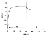
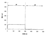
- the photoelectric element according to the present embodiment has high power storage performance. That is, the open circuit voltage maintenance rate is high when light is irradiated to the photoelectric element and then the light to the photoelectric element is shielded.
- the open-circuit voltage maintenance rate is A (V) when the photoelectric element is irradiated with 200 lux of light for 300 seconds, and the irradiation of light to the photoelectric element is blocked at the time point,
- B (V) When the open-circuit voltage of the photoelectric element when the state is maintained for 5 minutes is B (V), it is expressed as a percentage of B with respect to A ((B / A) ⁇ 100 (%)).
- the open-circuit voltage maintenance ratio can be 10% or more.
- a and B can satisfy the following relational expression. (B / A) ⁇ 100 ⁇ 10 This is presumed to be because the movement of the holes held in the hole transport layer 4 to the mediator (electron transport material forming the electron transport layer) is suppressed in this embodiment.
- the mediator electron transport material forming the electron transport layer
- the organic compound constituting the electron transport layer 3 and the hole transport layer 4 has a redox part that can be repeatedly redox as a part of the molecule, and an electrolyte solution as the other part.
- the electron transport layer 3 may be composed of an organic compound (second organic compound), and the second gel layer 7 may be composed of the second organic compound and the electrolyte solution.
- the 1st electrode 2 which consists of a layer of a transparent conductive oxide comprised by indium oxide, tin oxide, zinc oxide etc. on the 1st base material 1, glass
- the first electrode 2 may be formed on a light-transmitting first base material 1 made of a resin or the like by a vacuum process such as sputtering or vapor deposition, spin coating, spraying, screen printing, etc.
- the first electrode 2 may be formed by a wet method.
- a second substrate such as the first substrate 1 may be disposed on the surface of the second electrode 5 opposite to the hole transport layer 4. In that case, the second electrode 5 may be formed on the second substrate in the same manner as the first electrode 2.
- the second organic compound having the oxidation-reduction part and the gel part as described above in one molecule is represented by the following general formula, for example, like the first organic compound.
- (X i ) nj : Y k (X i ) n and (X i ) nj represent a gel site, and X i represents a monomer of a compound that forms the gel site.
- the gel site can be composed of a polymer backbone.
- Y represents a redox moiety bonded to X.
- j and k are each an arbitrary integer representing the number of (X i ) n and Y contained in one molecule, and both are preferably in the range of 1 to 100,000.
- the redox moiety Y may be bonded to any part of the polymer skeleton constituting the gel part (X i ) n and (X i ) nj .
- the oxidation-reduction part Y may contain different types of materials (atomic groups). In this case, materials (atomic groups) having a close oxidation-reduction potential are preferable from the viewpoint of the electron exchange reaction.
- the second organic compound that has a redox moiety and a gel site in one molecule and functions as the electron transport layer 3 contains a polymer or imide having a quinone derivative skeleton formed by chemically bonding quinones.
- a polymer having an imide derivative skeleton examples thereof include a polymer having an imide derivative skeleton, a polymer having a phenoxyl derivative skeleton containing phenoxyl, and a polymer having a viologen derivative skeleton containing viologen.
- the polymer skeleton is a gel site
- the quinone derivative skeleton, the imide derivative skeleton, the phenoxyl derivative skeleton, and the viologen derivative skeleton are redox portions.
- examples of the polymer having a quinone derivative skeleton in which quinones are chemically bonded include compounds having chemical structures represented by the following [Chemical Formula 22] to [Chemical Formula 25].
- R represents methylene, ethylene, propane-1,3-dienyl, ethylidene, propane-2,2-diyl, alkanediyl, benzylidene, propylene, vinylidene, propene-1,3- Saturated or unsaturated hydrocarbons such as diyl, but-1-ene-1,4-diyl; cyclic hydrocarbons such as cyclohexanediyl, cyclohexenediyl, cyclohexadienediyl, phenylene, naphthalene, biphenylene; oxalyl, malonyl, succinyl, Glutanyl, adipo
- [Chemical Formula 22] is an example of an organic compound formed by chemically bonding anthraquinone to the polymer main chain.
- [Chemical Formula 23] is an example of an organic compound constituted by incorporating anthraquinone as a repeating unit into a polymer main chain.
- [Chemical Formula 24] is an example of an organic compound in which anthraquinone is a cross-linking unit.
- [Chemical Formula 25] is an example of anthraquinone having a proton donating group that forms an intramolecular hydrogen bond with an oxygen atom.
- Examples of the polymer having an imide derivative skeleton in which the redox moiety Y contains an imide include polyimides represented by [Chemical Formula 26] and [Chemical Formula 27].
- examples of R 1 to R 3 include aromatic groups such as a phenylene group, aliphatic chains such as alkylene groups and alkyl ethers, and ether groups.
- the above polyimide is obtained by thermal imidization.
- the polyimide polymer skeleton may be cross-linked at the R 1 to R 3 portions. If the second organic compound only swells in the solvent and does not elute, the polyimide polymer skeleton need not have a crosslinked structure.
- the portions correspond to the gel sites (X i ) n and (X i ) nj .
- an imide group may be contained in the crosslinked unit.
- the imide group phthalimide, pyromellitic imide, and the like are preferable as long as they exhibit electrochemically reversible redox characteristics.
- Examples of the polymer having a phenoxyl derivative skeleton containing phenoxyl include a galbi compound (galbi polymer) as shown in [Chemical Formula 28].
- the galbi compound corresponds to the redox moiety Y
- the polymer skeleton corresponds to the gel sites (X i ) n and (X i ) nj .
- Examples of the polymer having a viologen derivative skeleton containing viologen include polyviologen polymers as shown in [Chemical Formula 30] and [Chemical Formula 31].
- [Chemical Formula 32] corresponds to the redox moiety Y
- the polymer skeleton corresponds to the gel sites (X i ) n and (X i ) nj .
- m and n represent the degree of polymerization of the monomer, A range of 100,000 is preferred.
- the organic compound having the above redox portion and polymer skeleton forms the gel layer 6 by swelling the polymer skeleton containing an electrolyte solution between the skeletons.
- the electron transport layer 3 contains the electrolyte solution, the ionic state formed by the redox reaction of the redox portion is compensated by the counter ion in the electrolyte solution, and the redox portion is stabilized.
- the electron transport layer 3 is configured so that the oxidation-reduction potential is noble with respect to the hole transport layer 4. That is, the potential of the electrode 2 provided with the electron transport layer 3 becomes nobler than the potential of the electrode 5 provided with the hole transport layer 4, thereby achieving high output of the photoelectric element. . From a different viewpoint, it can be said that the redox potential of the hole transport layer 4 is lower than that of the electron transport layer 3.
- the electron transport layer 3 becomes the hole transport layer 4.
- the oxidation-reduction potential of the second organic compound constituting the electron transport layer 3 depends on the oxidation of the first organic compound constituting the hole-transport layer 4. Be more noble than the reduction potential. In other words, the redox potential of the first organic compound constituting the hole transport layer 4 is made lower than the redox potential of the second organic compound constituting the electron transport layer 3.
- one of the two gel layers can function as the electron transport layer 3 and the other functions as the hole transport layer 4.
- the gel layer 6 which comprises the electron carrying layer 3 exhibits the function approximated to the n-type semiconductor, and it can be said that it is n-gel (n-type gel layer).
- the gel layer 7 constituting the hole transport layer 4 exhibits a function similar to that of a p-type semiconductor and can be said to be a p-gel (p-type gel layer). That is, in this case, the photoelectric element is an element formed by sandwiching a gel-like body composed of n-gel and p-gel between the electrodes 2 and 5.
- the potential difference between the electron transport layer 3 and the hole transport layer 4 (potential difference in which the electron transport layer 3 has a noble oxidation-reduction potential with respect to the hole transport layer 4) is that the electron transport layer 3 and the hole transport layer 4 are It is obtained by being composed of an organic compound as described above. That is, the redox potential of the second organic compound constituting the electron transport layer 3 described above is higher than that of the first organic compound constituting the hole transport layer 4 described above.
- the potential difference between the electron transport layer 3 and the hole transport layer 4 is preferably 200 mV or more and 2000 mV or less. If this potential difference is less than 200 mV, it is difficult to obtain a high open circuit voltage of the photoelectric element, and it may be difficult to produce a high output. When this potential difference exceeds 2000 mV, the light energy available for photoelectric conversion in the photoelectric element increases, and only light in the short wavelength region is used for photoelectric conversion, which makes it difficult to obtain a high output. There is a fear.
- the thicknesses of the electron transport layer 3 and the hole transport layer 4 are each preferably in the range of 10 nm to 10 mm, particularly in the range of 100 nm to 100 ⁇ m, from the viewpoint of maintaining good electron or hole transport properties. preferable. If it is this thickness, the improvement of the transport characteristic of an electron or a hole and the enlargement of the interface area will be compatible at a higher level.
- the electrode 2, the electron transport layer 3, the hole transport layer 4, and the second electrode 5 may be sequentially stacked in this order, or in the reverse order.
- 2 is provided with an electron transport layer 3
- a second electrode 5 is provided with a hole transport layer 4
- the first electrode 2 and the second electrode 5 are A method may be employed in which the layer 3 and the hole transport layer 4 are overlapped and stacked on the surface on which the layer 3 and the hole transport layer 4 are provided.
- the layer of the electrolyte solution may be formed between the electron transport layer 3 and the hole transport layer 4 as well as when the electron transport layer 3 and the hole transport layer 4 are in contact with each other. That is, an electrolyte solution layer that does not constitute the gel layers 6 and 7 may be formed between the first gel layer 6 and the second gel layer 7.
- a wet forming method of applying a solution containing an organic compound or the like Is preferable because it is a simpler and lower cost production method.
- a wet forming method is preferable from the viewpoint of moldability.
- the wet process include a spin coating method, a drop casting method in which droplets are dropped and dried, and a printing method such as screen printing and gravure printing.
- a vacuum process such as a sputtering method or a vapor deposition method may be employed.
- the electrolyte solution penetrates each organic compound. As a result, these organic compounds are swollen to form the gel layers 6 and 7.
- This electrolyte solution also functions as a medium for smooth movement of charges in the gel layers 6 and 7.
- This electrolyte solution also has a function of stabilizing the redox state of the redox moiety in the organic compound. The electrolyte solution stabilizes, in particular, the reduced state of the redox part in the second organic compound constituting the electron transport layer 3 in the second gel layer 7.
- the electrolyte solution stabilizes, in particular, the oxidation state of the redox part in the first organic compound constituting the hole transport layer 4 in the first gel layer 6.
- the electrolyte solution stabilizes, in particular, the oxidation state of the redox part in the first organic compound constituting the hole transport layer 4 in the first gel layer 6.
- the electrolyte solution includes an electrolyte and a solvent. If it is.
- the electrolyte include a supporting salt and a redox constituent material composed of an oxidant and a reductant, and either or both of them may be used.
- Examples of the supporting salt include tetrabutylammonium perchlorate, tetraethylammonium hexafluorophosphate, ammonium salts such as imidazolium salt and pyridinium salt, alkali metals such as lithium perchlorate and potassium tetrafluoroborate.
- Examples include salt.
- the redox-system constituent means a substance that exists reversibly in the form of an oxidant and a reductant in a redox reaction.
- redox-based constituent materials include chlorine compound-chlorine, iodine compound-iodine, bromine compound-bromine, thallium ion (III) -thallium ion (I), mercury ion (II) -mercury ion (I ), Ruthenium ion (III) -ruthenium ion (II), copper ion (II) -copper ion (I), iron ion (III) -iron ion (II), nickel ion (II) -nickel ion (III), Examples thereof include, but are not limited to, vanadium ion (III) -vanadium ion (II), manganate ion-permanganate ion, and the like.
- Such a redox component constitutes a function different from the redox part in the electron transport layer 3 and the hole transport layer 4.
- the electrolyte solution layer exists as described above, that is, the electrolyte solution layer that does not constitute the first gel layer 6 and the second gel layer 7 is present between the electron transport layer 3 and the hole transport layer 4. If present, this layer of electrolyte solution may be held in a polymer matrix.
- the polyvinylidene fluoride polymer compound used as the polymer matrix include a homopolymer of vinylidene fluoride or a copolymer of vinylidene fluoride and other polymerizable monomers, and preferably vinylidene fluoride. And a copolymer of a radically polymerizable monomer.
- copolymerizable monomers examples include hexafluoropropylene, tetrafluoroethylene, trifluoroethylene, ethylene, propylene, acrylonitrile, and vinylidene chloride. , Methyl acrylate, ethyl acrylate, methyl methacrylate, styrene and the like.
- the solvent constituting the electrolyte solution includes, for example, at least one of water, an organic solvent, and an ionic liquid.
- the solvent of the electrolyte solution When water or an organic solvent is used as the solvent of the electrolyte solution, the reduction state or oxidation state of the redox part of the organic compound is stabilized, and electrons and holes are transported more stably.
- the solvent any of an aqueous solvent and an organic solvent can be used, but an organic solvent excellent in ion conductivity is preferable in order to stabilize the redox moiety.
- organic solvent examples include carbonate compounds such as dimethyl carbonate, diethyl carbonate, methyl ethyl carbonate, ethylene carbonate and propylene carbonate, ester compounds such as methyl acetate, methyl propionate and ⁇ -butyrolactone, diethyl ether, 1,2 -Ether compounds such as dimethoxyethane, 1,3-dioxosilane, tetrahydrofuran, 2-methyl-tetrahydrofuran, heterocyclic compounds such as 3-methyl-2-oxazozirinone, 2-methylpyrrolidone, acetonitrile, methoxyacetonitrile, propionitrile, etc.
- carbonate compounds such as dimethyl carbonate, diethyl carbonate, methyl ethyl carbonate, ethylene carbonate and propylene carbonate
- ester compounds such as methyl acetate, methyl propionate and ⁇ -butyrolactone
- diethyl ether 1,2 -Eth
- the solvent is a carbonate compound such as ethylene carbonate or propylene carbonate, ⁇ -butyrolactone, 3-methyl-2- Preferred are heterocyclic compounds such as oxazozirinone and 2-methylpyrrolidone, and nitrile compounds such as acetonitrile, methoxyacetonitrile, propionitrile, 3-methoxypropionitrile and valeric nitrile.
- the action of stabilizing the redox moiety by the electrolyte solution is particularly improved.
- the ionic liquid is not volatile and has high flame retardancy, it has excellent stability.
- all known ionic liquids can be used.
- 1-ethyl-3-methylimidazolium tetracyanoborate such as imidazolium, pyridine, alicyclic amine, aliphatic amine, azo Nitrogen-based ionic liquids, European Patent No. 718288 specification, International Publication WO95 / 18456 pamphlet, Electrochemistry Vol.65, No.11, 923 (1997), J. Electrochem. Soc.143, No.10 3099 (1996), Inorg.orgChem. 35, 1168 (1996).
- the concentration of the electrolyte solution that is, the amount of the electrolyte with respect to the total amount of the electrolyte solution (the total amount of the electrolyte and the solvent) is preferably 0.1 to 10 mol / L.
- concentration of the electrolyte solution falls within this range, the redox state in which the redox portion of the organic compound is generated is further stabilized.
- the electrolyte solution is swollen by the organic compound of the electron transport layer 3 and the hole transport layer 4 and becomes a part of the gel layers 6 and 7.
- the first gel layer 6 is formed by the first organic compound constituting the hole transport layer 4 being swollen by the electrolyte solution
- the electrolyte solution that has permeated the hole transport layer 4 is the first gel layer 6. It has become a part of.
- the second gel layer 7 is formed by the first organic compound constituting the electron transport layer 3 being swollen by the electrolyte solution
- the electrolyte solution penetrating the electron transport layer 3 is one of the second gel layers 7. Has become a department.
- the electrolyte solution does not exist in a liquid state (flowable state) or is only a part even in a liquid state and its amount is small.
- the gel layers 6 and 7 support the electrolyte solution, it is possible to provide an optoelectric device that does not have a problem of leakage of the electrolyte solution.
- the first gel layer 6 and the second gel The degree of swelling of the layer 7 is preferably 110 to 3000%, more preferably 150 to 500%. If it is less than 110%, the electrolyte component in the gel is small, so there is a possibility that the redox part cannot be sufficiently stabilized. If it exceeds 3000%, the redox part in the gel is small. Since the electron transport capability may be reduced, the characteristics of the photoelectric element may be deteriorated in any case.
- the photoelectric element is preferably the electron transport layer 3. And / or a hole transport layer 4 is provided with a sensitizing dye that performs an electron transfer reaction.
- the photoelectric element includes a sensitizing dye, the photoelectric conversion efficiency of the photoelectric element is further improved.
- the electron transfer reaction is a reaction that interacts to give and receive electrons to one or both of the electron transport layer 3 and the hole transport layer 4.
- the electron transport layer 3 and the hole transport layer 4 usually have an action of imparting electrons to the other.
- the sensitizing dye when the sensitizing dye receives electrons from the electron transport layer 3, this sensitizing dye usually exerts an action of imparting electrons to the hole transport layer 4.
- the sensitizing dye exhibits an effect of imparting electrons to the electron transport layer 3. From a different viewpoint, it can also be said to be a hole transfer reaction for transferring holes.
- the sensitizing dye known materials as described above can be used. Specifically, D131 and K19 described later can be exemplified. Among these, a dye having an associative property on the film is preferable from the viewpoint of promoting charge separation during photoelectric conversion in order to densely fill and cover the film surface. As a dye having an effect by forming an aggregate, for example, a dye represented by the structural formula of the above [Chemical Formula 17] is preferable. In this case, recombination of electrons and holes present in the electron transport material and the hole transport material is dramatically reduced, and thus the conversion efficiency of the photoelectric conversion element is improved.
- the sensitizing dye is present in the gel layers 6 and 7, and in particular, the physical or chemical action between the sensitizing dye and the organic compound constituting the gel layers 6 and 7, etc.
- the gel layers 6 and 7 are preferably immobilized. That is, the sensitizing dye is fixed in the first gel layer 6 by a physical or chemical action between the sensitizing dye and the first organic compound constituting the first gel layer 6. It is preferable that the sensitizing dye is fixed in the second gel layer 7 by a physical or chemical action between the sensitizing dye and the second organic compound constituting the second gel layer 7. It is preferable that
- the sensitizing dye is present in the second gel layer 7 means that the sensitizing dye is not present only in the surface layer of the second gel layer 7 but also in the inside thereof. Means. Thereby, the state in which the amount of the sensitizing dye present in the second gel layer 7 is at or above a certain value is continuously maintained, and the output of the photoelectric element is improved.
- the “state where the sensitizing dye is present in the second gel layer 7” includes “the state where the sensitizing dye is present in the electrolyte solution constituting the second gel layer 7”, and “A state in which the sensitizing dye is present in the second gel layer 7 by physically and chemically interacting with the organic compound constituting the second gel layer 7”. It is preferable that the sensitizing dye is present throughout the second gel layer 7.
- the state in which the sensitizing dye is held in the second gel layer 7 by physical interaction with the second organic compound constituting the second gel layer 7 means, for example, The state in which the 2nd organic compound which comprises the gel layer 7 has a structure which prevents the movement of the molecule
- numerator of a sensitizing dye is mentioned.
- the structure that prevents the movement of the molecules of the sensitizing dye includes a structure in which the second organic compound exhibits steric hindrance due to various molecular chains such as an alkyl chain, or a void size that exists between the molecular chains of the second organic compound. Is a structure that is small enough to suppress the movement of molecules of the sensitizing dye.
- the sensitizing dye has a factor that expresses a physical interaction. Specifically, the molecular size of the sensitizing dye increases because the sensitizing dye has a structure that expresses steric hindrance due to various molecular chains such as an alkyl chain, and the sensitizing dye crosslinks. It is effective to have such a structure.
- the state in which the sensitizing dye is present in the second gel layer 7 by chemical interaction with the second organic compound constituting the second gel layer 7 means, for example, a covalent bond, an arrangement. Sensitization in the second gel layer 7 due to interactions such as potential bond, ionic bond, hydrogen bond, van der Waals bond, hydrophobic interaction, hydrophilic interaction, force based on electrostatic interaction Examples include a state in which the dye is retained. In particular, when the sensitizing dye is fixed in the second gel layer 7 by a chemical interaction between the sensitizing dye and the second organic compound constituting the second gel layer 7, The distance from the second organic compound approaches, and the efficiency of electron transfer becomes possible.
- a functional group is added to the second organic compound and the sensitizing dye. It is preferable that the sensitizing dye is fixed to the second organic compound by appropriate introduction and chemical reaction via this functional group.
- functional groups include hydroxyl groups, carboxyl groups, phosphate groups, sulfo groups, nitro groups, alkyl groups, carbonate groups, aldehyde groups, thiol groups, and the like.
- reaction format of the chemical reaction via the functional group include a condensation reaction, an addition reaction, and a ring-opening reaction.
- the functional group of the sensitizing dye is in the vicinity of a site where the electron density is increased in a state where the sensitizing dye is photoexcited. It is preferable that the functional group in the second organic compound in the second gel layer 7 is introduced in the vicinity of a site involved in electron transport in the second organic compound. In this case, the efficiency of electron transfer from the sensitizing dye to the second organic compound and the efficiency of electron transport in the second organic compound are improved.
- the sensitizing dye and the second organic compound constituting the second gel layer 7 are bonded by a linking group having a high electron transporting property that connects the electron cloud of the sensitizing dye and the electron cloud of the second organic compound.
- an ester bond having a ⁇ -electron system can be cited as a chemical bond that connects the ⁇ -electron cloud of the sensitizing dye and the ⁇ -electron cloud of the second organic compound.
- the timing at which the sensitizing dye and the second organic compound are bonded is such that when the second organic compound is in a monomer state, when the second organic compound is polymerized, after the second organic compound is polymerized, When the second organic compound gels, it may be any after the second organic compound gels.
- Specific examples of the method include a method of immersing the electron transport layer 3 formed of the second organic compound in a bath containing a sensitizing dye, and a coating liquid containing the second organic compound and the sensitizing dye.
- a method of forming the electron transport layer 3 by applying a film on the first electrode 2 may be used, and a plurality of methods may be combined.
- the content of the sensitizing dye in the second gel layer 7 is appropriately set, and in particular, if the content of the sensitizing dye is 0.1 parts by mass or more with respect to 100 parts by mass of the second organic compound, The amount of the sensitizing dye per unit film thickness of the second gel layer 7 is sufficiently increased, the light absorbing ability of the sensitizing dye is improved, and a high current value is obtained.
- the content of the sensitizing dye is 1000 parts by mass or less with respect to 100 parts by mass of the second organic compound, it is suppressed that an excessive amount of the sensitizing dye is interposed between the second organic compounds, Inhibition of electron transfer in the second organic compound by the sensitizing dye is suppressed, and high conductivity is ensured.
- the electron transport layer 3 and the hole transport layer 4 are formed as the gel layers 6 and 7, and further, a sensitizing dye that interacts with one or both of the electron transport layer 3 and the hole transport layer 4 is introduced.
- a photoelectric device having a sufficiently wide reaction interface and excellent conversion efficiency.
- This double power generation is in contact with each layer if the dye contacting the electron transport layer 3 and the dye contacting the hole transport layer 4 are different, that is, if a photoelectric device is formed by using a plurality of dyes.
- the dye is optimized, and it becomes possible to obtain a photoelectric device with higher output.
- the second organic compound that constitutes the electron transport layer 3 and the first organic compound that constitutes the hole transport layer 4 are suitable for an optoelectric device configured to have a redox portion and a gel part.
- the electron transport layer 3 and the hole transport layer 4 are formed of an organic compound having a redox portion that can be repeatedly redox.
- the organic compound is formed as the gel layers 6 and 7 including an electrolyte solution that stabilizes the reduction state of the redox portion. For this reason, in this photoelectric element, the structure is subdivided at the molecular level, the reaction interface becomes large, and electrons can be transported efficiently and at a high reaction rate.
- the redox part can be held in the vicinity of the electrode, or the adjacent redox part can be interposed between them. It is possible to hold the organic compound so that the distance is sufficiently close so that electrons can be exchanged.
- redox portions can be present in the electron transport layer 3 and the hole transport layer 4 at high density. Thereby, a very fast self-electron exchange reaction rate constant can be realized, and the electron transport capability can be enhanced.
- the electron transport layer 3 and the hole transport layer 4 as the gel layers 6 and 7 of the organic compound, it is possible to impart adhesiveness to these layers, or to impart flexibility and light transmittance. It will be easier.
- the redox part is present in the molecules of the organic compounds constituting the gel layers 6 and 7, the redox part is placed in the gel layer in a state where electron transport by repeated redox reactions is performed more effectively. 6 and 7 make it easier to hold. That is, since the oxidation-reduction part is chemically bonded to the organic compounds constituting the gel layers 6, 7, the oxidation-reduction part is placed in the gel layers 6, 7 so that the oxidation-reduction part remains at a position where electrons are easily transported. It can be held by.
- the positional relationship of the oxidation-reduction part in the organic compound may be, for example, a structure in which the oxidation-reduction part is arranged as a side chain with respect to the skeleton of the organic compound constituting the gel layers 6 and 7. And the redox moiety may be alternately or partially continuously arranged and bonded.
- the redox part is capable of transporting electrons not by diffusion but by an electron exchange reaction between the redox parts.
- This electron exchange reaction is a reaction in which electrons are exchanged between the redox parts by oxidizing the redox part in the reduced state, which is in close proximity to the redox part in the oxidized state. Holes are transported.
- the function is similar to that of ion-conducting materials in which ions are conducted by diffusion, but the above-described electron transport mechanism is different in that the redox part is not diffused but transported by exchanging electrons with the adjacent redox part. .
- the redox parts need to be close to each other in order to enable electron transfer.
- the distance traveled is expected to be a few angstroms because it is retained by layers 6 and 7.
- the reaction for electron exchange with the adjacent redox part is a reaction called a self-electron exchange reaction.
- the oxidation-reduction portion is held in the gel layers 6 and 7 as described above, so that the light can be supplied to the electricity or the electricity without impairing the electron transport property.
- the reaction field for conversion to light that is, the reaction interface can be enlarged, and a photoelectric element with high conversion efficiency can be obtained.
- the reaction interface is an interface between the electron transport layer and the hole transport material or electrolyte solution.
- the reaction interface is an interface between the electron transport layer and the hole transport material or electrolyte solution.
- the electron transport layer 3 and the hole transport layer 4 have an oxidation-reduction part in the organic compound containing an electrolyte solution, whereas the reaction interface area cannot be sufficiently increased in the past. 6 and 7, the reaction interface between the redox portion and the electrolyte solution penetrating into the gel layers 6 and 7 becomes large, and the conversion efficiency can be increased.
- the reaction interface becomes large.
- the conventional electron transport material made of an inorganic semiconductor or the like is an inorganic substance, and therefore it is difficult to fall below the nanometer scale even if it is finely divided.
- the hole transport layer 4 the structure can be subdivided at the molecular level and the area of the interface necessary for charge separation can be increased as long as the redox part can be oxidized and reduced to transport electrons.
- the interface can be theoretically formed on an angstrom scale.
- a special interface state that promotes charge separation is formed at the interface between the redox part of the organic compound and another layer or an electrolyte solution.
- the electron transport layer 3 and the hole transport layer 4 are formed of an organic compound having a redox portion, design and synthesis according to electrical properties such as potential and structural properties such as molecular size. In addition, the gelation and solubility control of the electron transport layer 3 and the hole transport layer can be performed.
- the electron transport layer 3 and the hole transport layer 4 are formed from an organic compound, high-temperature baking is not required as in the case where the layer of an electron transport material is formed from an inorganic substance such as an inorganic semiconductor. It is also possible to impart flexibility to these layers.
- organic compounds have no problems of resource depletion, low toxicity, and heat energy can be recovered by incineration at the time of disposal. Can be mentioned.
- the organic compound constituting the electron transport layer contains (permeates) the electrolyte solution, so that the redox state of the redox portion present in the organic compound is stabilized. Electrons are transported stably. That is, since an organic compound has an unstable redox state (oxidized state or reduced state) compared to an inorganic compound such as a metal semiconductor or a metal oxide semiconductor that is generally used as an electron transport material, an electron transport layer 3 and the hole transport layer 4 are difficult to be used as a material.
- the organic compound into a structure containing the electrolyte solution (the electrolyte solution permeates the organic compound), the ionic state formed by the redox reaction of the redox moiety is compensated by the counter ion in the electrolyte solution. Is done. That is, for example, the redox moiety that has become a cationic state is stabilized by the reverse charge of the anion in the electrolyte solution. Furthermore, the reduction state of the redox moiety is stabilized by the action of the solvation of the solvent and the dipole moment, and as a result, the redox part is stabilized. Since the electrolyte solution is held by the gel layers 6 and 7, liquid leakage does not occur in the photoelectric element.
- a photoelectric element formed by sandwiching an electron transport layer and a hole transport layer between a pair of electrodes as described above
- a power generation element by photoelectric conversion such as a photovoltaic cell or a solar cell, or a light emitting element such as an organic EL
- an optical display element such as an electronic display element or electronic paper, a sensor element that senses temperature, light, or the like can be formed by using a photoelectric element or the like.
- Example 1 Synthesis of TEMPO-substituted norbornene monomer
- 2.0 g (12.2 mmol) of 5-norbornene-2,3-carboxylic acid anhydride was dissolved in 180 ml of benzene, 4.2 g (24.4 mmol) of 4-hydroxy-TEMPO, 2.4 ml of triethylamine (TEA) (17. 2 mmol) and 4-dimethylaminopyridine (DMAP) 0.63 g (5.15 mmol) were added, and the mixture was stirred at reflux for 12 hours.
- TEA triethylamine
- DMAP 4-dimethylaminopyridine
- a TEMPO-substituted norbornene polymer consisting of a repeating unit represented by the formula: As a result of measuring the molecular weight of the obtained TEMPO-substituted norbornene polymer by using gel permeation chromatography (GPC) (Column Tosoh Co., Ltd.
- a conductive glass substrate having a thickness of 0.7 mm and a sheet resistance of 100 ⁇ / ⁇ was prepared as the base material 8 on which the second electrode 5 was provided.
- the conductive glass substrate is composed of a glass substrate and a coating film made of fluorine-doped SnO 2 laminated on one surface of the glass substrate.
- the glass substrate is a base material 8 and the coating film is a second electrode. 5
- An isopropyl alcohol solution in which 5 mM chloroplatinic acid was dissolved was spin-coated on the conductive glass substrate, and then baked at 400 ° C. for 30 minutes.
- the conductive glass substrate provided with the hole transport layer 4 and the conductive glass substrate treated with platinum chloride are arranged so that the hole transport layer 4 and the platinum chloride treated surface face each other.
- a hot-melt adhesive having a width of 1 mm and a thickness of 50 ⁇ m (manufactured by DuPont, Binell) was interposed at the outer edge between the two.
- the two conductive glass substrates were bonded via the hot melt adhesive by pressing the two conductive glass substrates in the thickness direction while heating the hot melt adhesive.
- a void serving as an electrolyte injection port was formed.
- an electrolytic solution was filled between the hole transport layer 4 and the conductive glass substrate treated with platinum chloride from the inlet.
- the injection port was filled by irradiating UV light to cure the UV curable resin.
- the electron transport layer 3 made of an electrolytic solution was formed, and the electrolytic solution was permeated into the hole transport layer 4 to swell the PTNB constituting the hole transport layer 4, thereby forming the gel layer 6.
- an aqueous solution containing methyl viologen represented by [Chemical Formula 19] at a concentration of 0.02 M and potassium chloride 1 M was used as the electrolytic solution.
- the photoelectric element was produced by the above.
- Nitroxyamide was synthesized by the procedure shown in the following [Chemical Formula 37]. Specifically, benzene (60 ml) was added to 2.8 ml (16 mmol) of 4-amino-2,2,6,6, -tetramethylpiperidine, cooled to a temperature of 0 ° C., stirred, and then acryloyl chloride 1 .3 ml (16 mmol) was added dropwise, cooled at 0 ° C. for 1 hour, and stirred at room temperature overnight to precipitate crystals. Next, after removing the solvent, the product was purified by recrystallization to obtain the product of Scheme 2 of [Chemical Formula 37] in a yield of 54%.
- Example 3 As the electrolytic solution, an acetonitrile solution containing 0.01M galbinohydroxy radical shown in [Chemical Formula 18], 0.0025M N-methylbenzimidazole, and 0.01M lithium perchlorate was used. Other than that, a photoelectric element was fabricated under the same conditions as in Example 1.
- Example 4 In Example 1, in forming the hole transport layer and supporting the dye, 10 mg of nitroxyamide and 3 mg of the sensitizing dye (D131) were dissolved in 1 ml of THF (tetrahydrofuran), and the obtained solution was used as a conductive glass substrate. Drop cast on top. As a result, a hole transport layer having a thickness of 100 nm carrying the sensitizing dye was formed.
- THF tetrahydrofuran
- Example 5 In Example 1, in forming the hole transport layer and supporting the dye, 10 mg of nitroxyamide was first dissolved in 1 ml of THF (tetrahydrofuran), and the resulting solution was drop-cast on a conductive glass substrate. Thereby, a hole transport layer having a thickness of 100 nm was formed. Subsequently, this hole transport layer was spin-coated with a saturated solution of sensitizing dye (D131) in acetonitrile, thereby supporting the sensitizing dye on the hole transport layer.
- THF tetrahydrofuran
- the transparent conductive glass provided with the electron transport layer 3 was immersed in a saturated solution of sensitizing dye (D131) in acetonitrile for 1 hour. Thereafter, it was washed with acetonitrile for 5 minutes in order to remove excess dye.
- sensitizing dye D131
- an isopropyl alcohol solution in which 5 mM chloroplatinic acid was dissolved was spin-coated on another conductive glass substrate 1 and then baked at 400 ° C. for 30 minutes.
- the conductive glass substrate provided with the electron transport layer 3 and the conductive glass substrate treated with platinum chloride are disposed so that the electron transport layer 3 and the platinum chloride treated surface face each other.
- a hot-melt adhesive having a width of 1 mm and a thickness of 50 ⁇ m (manufactured by DuPont, Binell) was interposed on the outer edge.
- the two conductive glass substrates were bonded via the hot melt adhesive by pressing the two conductive glass substrates in the thickness direction while heating the hot melt adhesive.
- a void serving as an electrolyte injection port was formed.
- an electrolytic solution was filled between the electron transport layer 3 and the conductive glass substrate treated with platinum chloride from the injection port.
- the injection port was filled by irradiating UV light to cure the UV curable resin.
- an aqueous solution containing methyl viologen at a concentration of 0.02M and potassium chloride at a concentration of 1M was used as the electrolytic solution.
- the photoelectric element was produced by the above.
- each photoelectric element was placed in a light-shielding container for 300 seconds (5 minutes), and the open voltage of the photoelectric element was measured by the same method as described above.
- the measurement result of the open circuit voltage for Example 1 is shown in FIG. 3, and the measurement result of the open circuit voltage for Comparative Example 1 is shown in FIG.
- Example 1 the open-circuit voltage maintenance rate was 70% or more, and the battery performance was high. On the other hand, in the comparative example 1, the open circuit voltage maintenance rate was less than 1%.
- the second gel layer 6 composed of the electron transport layer 3 is n-gel
- the first gel layer 7 composed of the hole transport layer 4 is p-gel.
- PV10 (1.95 g, Yield: 65%) as a pale yellow powder. did it.
- the structure of PV10 was measured by NMR, whereby the degree of polymerization was 10, the molecular weight was about 3200, and it could be identified as PV10.
- the molecular weight is a number average molecular weight, and the molecular weight can be measured by gel permeation chromatography.
- the molecular weight and measurement thereof are the same for the following polymers.
- PV10 aqueous solution 0.1 M, 10 ml, 1 mmol
- concentration is a value calculated by the molecular weight per unit of the polymer.
- first film On this first film, a 5 wt% aqueous solution of PV10 was spin-coated at 6000 rpm, and a 40 nm thick film (second film) was laminated. The first film and the second film were immersed in a saturated acetonitrile solution of the sensitizing dye D131 shown in [Chemical Formula 36] for 1 hour, and then washed with acetonitrile for 5 minutes to remove excess dye, whereby the third film was removed. Film (a film obtained by supporting the dye D131 on the first film and the second film).
- the above monomer (TEMPO-substituted norbornene monomer) consists of two isomers, an endo-, endo-derivative and an endo-, exo-derivative, but was used for the polymerization in the form of a mixture.
- the reaction solution was brought to room temperature and purified by reprecipitation using 200 ml of diethyl ether.
- the resulting pale orange powder was collected by filtration with a glass filter G4, and this pale orange powder was dried under reduced pressure at 50 ° C. for 10 hours. .
- 87 mg of a TEMPO-substituted norbornene monomer-bifunctional monomer crosslinked copolymer (PTNB) having a repeating unit and a crosslinked structure was obtained.
- the molecular weight of the polymer was 8000.
- the above-mentioned film was irradiated with UV for 60 seconds to crosslink PTNB to form a PTNB film.
- FTO substrate another conductive glass substrate (FTO substrate) different from the above substrate was prepared.
- a solution obtained by dissolving chloroplatinic acid in isopropyl alcohol so as to have a concentration of 5 mM is spin-coated and then baked at 400 ° C. for 30 minutes to form a pair.
- a second electrode 5 was formed.
- the conductive glass substrate (a substrate on which the electron transport layer 3 and the hole transport layer 4 and the like are laminated) and another conductive glass substrate on which the second electrode 5 is formed, While arrange
- the two conductive glass substrates were bonded via the hot melt adhesive by pressing the two conductive glass substrates in the thickness direction while heating the hot melt adhesive.
- an electrolytic solution was filled from the inlet.
- an acetonitrile solution containing LiTFSI at a concentration of 0.5M and N-methylbenzimidazole at a concentration of 1.6M was used.
- a UV curable resin was applied to the electrolyte solution injection port, and then the UV curable resin was cured by irradiating UV light, thereby filling the injection port.
- benzene 60 ml was added to 2.8 ml (16 mmol) of 4-amino-2,2,6,6, -tetramethylpiperidine, cooled to a temperature of 0 ° C., stirred, and then 1.3 ml of acryloyl chloride ( 16 mmol) was added dropwise, cooled at 0 ° C. for 1 hour, and stirred at room temperature overnight to precipitate crystals.
- the product was purified by recrystallization to obtain the product (2) in the scheme in a yield of 54%.
- PV10 film (film C) was produced by the same material and method as in Example 6.
- a photoelectric element was produced by the same material and method as in Example 6 except that the nitroxyamide film was used instead of the PTNB film.
- orange microcrystals of p-hydrogalvinoxyl styrene (1.54 g; 2.93 mmol) indicated by the product (3) in the scheme were obtained.
- a conductive glass substrate having a thickness of 0.7 mm and a sheet resistance of 100 ⁇ / ⁇ was prepared as the base material 1 on which the electrode 2 was provided.
- the conductive glass substrate is composed of a glass substrate and a coating film made of fluorine-doped SnO 2 laminated on one surface of the glass substrate.
- the glass substrate is a first base material 1 and the coating film is a first film.
- One electrode 2 is formed.
- the above galbi polymer (product (4) in the scheme) was dissolved in chlorobenzene at a ratio of 2% by mass. This solution is spin-coated at 2000 rpm on the electrode 2 of the conductive glass substrate and dried at 60 ° C. and 0.01 MPa for 1 hour to form a galbi polymer film (electron transport layer 3) having a thickness of 60 nm. did.
- This galbi polymer film was immersed in a saturated solution of sensitizing dye (D131) in acetonitrile for 1 hour.
- photoelectric element was produced by the same material and method as Example 6 except having used the galbi film instead of the PV10 film.
- Formation of electron transport layer Film formation of quinone polymer
- first base material 1 and first electrode 2 10 mg of the above polymer was dissolved in 0.1 g of N-methylpyrrolidone, spin-coated on the FTO substrate at 1000 rpm, and a thickness of 100 nm. A film was prepared.
- the quinone polymer film was immersed in an acetonitrile solution in which D131 was saturated and dissolved for 1 hour to perform a dye-supporting treatment.
- photoelectric element was produced by the same material and method as Example 6 except having used the quinone polymer film instead of the PV10 film.
- Example 10 (Formation of electron transport layer) An electron transport layer 3 was formed in the same manner as in Example 6. That is, PV10 (polydecyl viologen) and PV10-PSS complex were synthesized, these were formed on an FTO substrate, and D131 was supported thereon to form the electron transport layer 3.
- PV10 polydecyl viologen
- PV10-PSS complex were synthesized, these were formed on an FTO substrate, and D131 was supported thereon to form the electron transport layer 3.
- a norbornene-based crosslinked copolymer (PTNB) was synthesized by the same method as in Example 6.
- FTO substrate another conductive glass substrate (FTO substrate) different from the substrate on which PV10 was formed as the substrate (first base material 1 and first electrode 2) was used, PTNB 19.8 mg, ethyl lactate 0
- BACTC crosslinking agent
- PTNB was crosslinked by irradiating the film with UV for 60 seconds.
- this membrane was immersed in a D131 saturated acetonitrile solution for 1 hour, and then washed with acetonitrile for 5 minutes to remove excess dye.
- Conductive glass substrate (substrate on which the electron transport layer 3 is formed) provided with PV10 carrying D131, and conductive glass substrate (substrate on which the hole transport layer 4 is formed) provided with PTNB carrying D131 ) was placed so that the PV10 layer and the PTNB layer were opposed to each other, and a hot-melt adhesive having a width of 1 mm and a thickness of 50 ⁇ m (Bunel, manufactured by DuPont) was interposed at the outer edge between them.
- the two conductive glass substrates were bonded via the hot melt adhesive by pressing the two conductive glass substrates in the thickness direction while heating the hot melt adhesive.
- an electrolytic solution was filled from the inlet.
- an aqueous solution containing 0.1 M methyl viologen, 0.01 M compound of the chemical formula [Chemical Formula 40], and 0.1 M LiClO 4 was used.
- a UV curable resin was applied to the electrolyte solution injection port, and then the UV curable resin was cured by irradiating UV light, thereby filling the injection port.
- Example 11 (Formation of electron transport layer) An electron transport layer 3 was formed in the same manner as in Example 6. That is, PV10 (polydecyl viologen) and PV10-PSS complex were synthesized, these were formed on an FTO substrate, and D131 was supported thereon to form the electron transport layer 3.
- PV10 polydecyl viologen
- PV10-PSS complex were synthesized, these were formed on an FTO substrate, and D131 was supported thereon to form the electron transport layer 3.
- a hole transport layer was formed in the same manner as in Example 10 except that K19 dye represented by [Chemical Formula 41] was used instead of D131.
- a norbornene-based crosslinked copolymer (PTNB) was formed into a film by the same method as in Example 10, and a hole transport layer was formed by UV irradiation.
- PTNB norbornene-based crosslinked copolymer
- this film was immersed in a saturated acetonitrile solution of K19 dye represented by [Chemical Formula 41] for 1 hour, and then washed with acetonitrile for 5 minutes to remove excess dye.
- a conductive glass substrate (substrate on which the electron transport layer 3 is formed) provided with PV10 carrying D131 and a conductive glass substrate (hole transport layer 4) provided with PTNB carrying K19 are formed.
- a hot melt adhesive was interposed, and the adhesive was heated and pressed in the thickness direction while being bonded.
- the electrolyte solution was filled from the injection port, and the injection port was filled with a UV curable resin.
- chloroplatinic acid is dissolved in isopropyl alcohol so as to have a concentration of 5 mM, and the obtained solution is spin-coated on the coating film of the conductive glass substrate and then baked at 400 ° C. for 30 minutes. A second electrode 5 to be a pair was formed.
- the substrate provided with the galbi polymer film and the second electrode 5 were joined in the same manner as in Example 10, and the electrolyte was injected.
- the electrolytic solution 2,2,6,6-tetramethylpiperidine-1-oxyl is 1M
- sensitizing dye (D131) is 2 mM
- LiTFSI is 0.5M
- N-methylbenzimidazole is 1.6M.
- An acetonitrile solution containing in concentration was used.
- the conductive glass substrate provided with the galbi polymer film and the conductive glass substrate provided with the second electrode 5 are arranged so that the galbi polymer film and the second electrode 5 face each other, Bonding was performed by interposing a meltable adhesive and applying pressure while heating the adhesive. Next, the electrolyte solution was filled from the injection port, and the injection port was filled with a UV curable resin.
- the organic compound contained the electrolyte solution to form the gel layers 6 and 7, and the electrolyte solution did not exist in a highly fluid state.
- the electrolytic solution was present in a fluid state. Therefore, it was confirmed that the photoelectric elements of Examples 6 to 11 were less likely to cause liquid leakage than Comparative Example 2.
Abstract
Description
(B/A)×100≧10
本発明に係る光電気素子は、前記電子輸送層は繰り返し酸化還元が可能な酸化還元部を有する第二の有機化合物を備え、前記第二の有機化合物と前記電解質溶液とが第二のゲル層を構成し、前記電子輸送層の酸化還元電位が前記正孔輸送層の酸化還元電位よりも貴であってもよい。 The open-circuit voltage A (V) of the photoelectric element according to the present invention when the light of 200 lux is irradiated for 5 minutes and the open-circuit voltage B (5 minutes after the light is shielded at this time) V) may satisfy the following relational expression.
(B / A) × 100 ≧ 10
In the photoelectric element according to the present invention, the electron transport layer includes a second organic compound having a redox portion capable of repeated redox, and the second organic compound and the electrolyte solution are the second gel layer. The redox potential of the electron transport layer may be more noble than the redox potential of the hole transport layer.
(B/A)×100≧10
本実施形態に係る光電気素子は、次のように構成されてもよい。 The photoelectric device according to the present embodiment has an open circuit voltage A (V) at the time when 200 lux light is irradiated for 5 minutes, and an open circuit voltage B at the time when 5 minutes have passed since the light was shielded at this time. (V) preferably satisfies the following relational expression.
(B / A) × 100 ≧ 10
The photoelectric element according to the present embodiment may be configured as follows.
ゲル乾燥体とは、第一のゲル層6又は第二のゲル層7を乾燥させることで得られるものを指す。第一のゲル層6又は第二のゲル層7を乾燥させるとは、第一のゲル層6又は第二のゲル層7に内包される溶液を除去すること、特に溶媒を除去することを指す。第一のゲル層6又は第二のゲル層7を乾燥させる方法としては、加熱、真空環境中で第一のゲル層6又は第二のゲル層7から溶液または溶媒を除去する方法や、他の溶媒での第一のゲル層6又は第二のゲル層7に内包される溶液または溶媒を除去する方法などが挙げられる。なお、他の溶媒で第一のゲル層6又は第二のゲル層7に内包される溶液または溶媒を除去するに際しては、内包される溶液または溶媒と親和性が高く、かつ、加熱、真空環境中で除去しやすい溶媒を選択することが、第一のゲル層6又は第二のゲル層7に内包される溶液または溶媒の効率的な除去効果をもたらす。 (Swelling degree) = (weight of gel) / (weight of dried gel) × 100 (%)
A gel dry body refers to what is obtained by drying the
(Xi)nおよび(Xi)njはゲル部位を示し、Xiはゲル部位を形成する化合物のモノマーを示す。ゲル部位はポリマー骨格で構成され得る。モノマーの重合度nは、n=1~10万の範囲が好ましい。YはXに結合している酸化還元部を示す。j,kはそれぞれ1分子中に含まれる(Xi)n、Yの数を表す任意の整数であり、いずれも1~10万の範囲が好ましい。酸化還元部Yはゲル部位(Xi)nおよび(Xi)njを構成しているポリマー骨格のいかなる部位に結合していてもよい。酸化還元部Yは種類の異なる材料(原子団)を含んでいてもよく、この場合は電子交換反応の観点から酸化還元電位が近い材料(原子団)が好ましい。 (X i ) nj : Y k
(X i ) n and (X i ) nj represent a gel site, and X i represents a monomer of a compound that forms the gel site. The gel site can be composed of a polymer backbone. The polymerization degree n of the monomer is preferably in the range of n = 1 to 100,000. Y represents a redox moiety bonded to X. j and k are each an arbitrary integer representing the number of (X i ) n and Y contained in one molecule, and both are preferably in the range of 1 to 100,000. The redox moiety Y may be bonded to any part of the polymer skeleton constituting the gel part (X i ) n and (X i ) nj . The oxidation-reduction part Y may contain different types of materials (atomic groups). In this case, materials (atomic groups) having a close oxidation-reduction potential are preferable from the viewpoint of the electron exchange reaction.


[化13]PTGE:Poly(TEMPO grycidylether)
[化14]PTNB:Poly(TEMPO norbornene)
[化15]PTAm:Poly(TEMPO acrylamide)
[化16]PPGE:Poly(PROXYL grycidylether)
である。 [Chemical 13] to [Chemical 16] are [Chemical 13] PTGE: Poly (TEMPO glycidylether).
[Chemical Formula 14] PTNB: Poly (TEMPO norbornene)
[Chemical 15] PTAm: Poly (TEMPO acrylamide)
[Chemical 16] PPGE: Poly (PROXYL glycidylether)
It is.


(B/A)×100≧10
これは、本実施形態では正孔輸送層4に保持された正孔の、メディエータ(電子輸送層を形成する電子輸送材料)への移動が抑制されるためであると推察される。このような蓄電性の高い光電気素子が電源として用いられると、光の照射の有無によって電力の供給が不安定化するようなことが抑制される。 The photoelectric element according to the present embodiment has high power storage performance. That is, the open circuit voltage maintenance rate is high when light is irradiated to the photoelectric element and then the light to the photoelectric element is shielded. The open-circuit voltage maintenance rate is A (V) when the photoelectric element is irradiated with 200 lux of light for 300 seconds, and the irradiation of light to the photoelectric element is blocked at the time point, When the open-circuit voltage of the photoelectric element when the state is maintained for 5 minutes is B (V), it is expressed as a percentage of B with respect to A ((B / A) × 100 (%)). In the photoelectric element according to this embodiment, the open-circuit voltage maintenance ratio can be 10% or more. That is, A and B can satisfy the following relational expression.
(B / A) × 100 ≧ 10
This is presumed to be because the movement of the holes held in the
(Xi)nおよび(Xi)njはゲル部位を示し、Xiはゲル部位を形成する化合物のモノマーを示す。ゲル部位はポリマー骨格で構成され得る。モノマーの重合度nは、n=1~10万の範囲が好ましい。YはXに結合している酸化還元部を示す。j,kはそれぞれ1分子中に含まれる(Xi)n、Yの数を表す任意の整数であり、いずれも1~10万の範囲が好ましい。酸化還元部Yはゲル部位(Xi)nおよび(Xi)njを構成しているポリマー骨格のいかなる部位に結合していてもよい。酸化還元部Yは種類の異なる材料(原子団)を含んでいてもよく、この場合は電子交換反応の観点から酸化還元電位が近い材料(原子団)が好ましい。 (X i ) nj : Y k
(X i ) n and (X i ) nj represent a gel site, and X i represents a monomer of a compound that forms the gel site. The gel site can be composed of a polymer backbone. The polymerization degree n of the monomer is preferably in the range of n = 1 to 100,000. Y represents a redox moiety bonded to X. j and k are each an arbitrary integer representing the number of (X i ) n and Y contained in one molecule, and both are preferably in the range of 1 to 100,000. The redox moiety Y may be bonded to any part of the polymer skeleton constituting the gel part (X i ) n and (X i ) nj . The oxidation-reduction part Y may contain different types of materials (atomic groups). In this case, materials (atomic groups) having a close oxidation-reduction potential are preferable from the viewpoint of the electron exchange reaction.


(TEMPO置換ノルボルネンモノマーの合成)
5-ノルボルネン-2,3-カルボン酸無水物2.0g(12.2mmol)をベンゼン180mlに溶解し、4-ヒドロキシ-TEMPO4.2g(24.4mmol)、トリエチルアミン(TEA)2.4ml(17.2mmol)、4-ジメチルアミノピリジン(DMAP)0.63g(5.15mmol)を加え、12時間還流攪拌した。放冷後、2-クロロ-1-メチルピリジニウムヨージド3.9g(15.2mmol)を加え、室温で12時間反応させた。反応後沈殿をろ過し、ろ液をエーテルで抽出し、水洗浄後、溶媒を除去した。これにより得られた残留物を、クロロホルム/ヘキサン/酢酸エチル(混合体積比6/3/1)を展開溶媒として、シリカゲルによりカラム精製した後、ヘキサン/ジクロロメタン(混合体積比8/2)により再結晶し、下記式[化33]で表されるTEMPO置換ノルボルネンモノマーを橙色結晶として得た(収率40%)。 [Example 1]
(Synthesis of TEMPO-substituted norbornene monomer)
2.0 g (12.2 mmol) of 5-norbornene-2,3-carboxylic acid anhydride was dissolved in 180 ml of benzene, 4.2 g (24.4 mmol) of 4-hydroxy-TEMPO, 2.4 ml of triethylamine (TEA) (17. 2 mmol) and 4-dimethylaminopyridine (DMAP) 0.63 g (5.15 mmol) were added, and the mixture was stirred at reflux for 12 hours. After allowing to cool, 3.9 g (15.2 mmol) of 2-chloro-1-methylpyridinium iodide was added and reacted at room temperature for 12 hours. After the reaction, the precipitate was filtered, the filtrate was extracted with ether, washed with water, and the solvent was removed. The residue thus obtained was subjected to column purification with silica gel using chloroform / hexane / ethyl acetate (mixing

10mlナス型フラスコ中でTEMPO置換ノルボルネン100mg(0.20mmol)をトルエン1.0mlに溶解した。なお、[化33]に示すモノマー(TEMPO置換ノルボルネンモノマー)は、endo-,endo-誘導体とendo-,exo-誘導体との2つの異性体から成るが、混合物のまま重合に使用した。この溶液に、第二世代Grubbs触媒2.3mg(0.00270mmol)を加え、Ar雰囲気下、40℃で12時間攪拌した。その後、室温にした後、ジエチルエーテル200mlを使用して再沈殿精製し、生じた薄橙色粉末をグラスフィルターG4でろ集し、50℃で10時間減圧乾燥を行うことにより、下記式[化34]で表される繰り返し単位からなるTEMPO置換ノルボルネンポリマーを得た。得られたTEMPO置換ノルボルネンポリマーの分子量を、クロロホルムを溶離液としたゲルパーミエーションクロマトグラフィー(GPC)(カラム東ソー株式会社製TSKgelGMHXL)を使用して測定した結果、数平均分子量30000(ポリスチレン換算)、分散度(重量平均分子量/数平均分子量)は1.2であった。 (Synthesis of TEMPO-substituted norbornene polymer (homopolymerization))
In a 10 ml eggplant type flask, 100 mg (0.20 mmol) of TEMPO-substituted norbornene was dissolved in 1.0 ml of toluene. The monomer (TEMPO-substituted norbornene monomer) shown in [Chemical Formula 33] consists of two isomers, an endo-, endo-derivative and an endo-, exo-derivative, but was used in the polymerization as a mixture. To this solution, 2.3 mg (0.00270 mmol) of the second generation Grubbs catalyst was added and stirred at 40 ° C. for 12 hours in an Ar atmosphere. Thereafter, the mixture was brought to room temperature, purified by reprecipitation using 200 ml of diethyl ether, and the resulting pale orange powder was collected by filtration with a glass filter G4 and dried under reduced pressure at 50 ° C. for 10 hours to obtain the following formula [Chemical Formula 34]. A TEMPO-substituted norbornene polymer consisting of a repeating unit represented by the formula: As a result of measuring the molecular weight of the obtained TEMPO-substituted norbornene polymer by using gel permeation chromatography (GPC) (Column Tosoh Co., Ltd. TSKgelGMMHXL) using chloroform as an eluent, the number average molecular weight was 30000 (polystyrene conversion), The degree of dispersion (weight average molecular weight / number average molecular weight) was 1.2.

第二の電極5が設けられた基材8として、厚み0.7mm、シート抵抗100Ω/□の導電性ガラス基板を用意した。この導電性ガラス基板はガラス基板と、このガラス基板の一面に積層された、フッ素ドープされたSnO2からなるコーティング膜とから構成され、前記ガラス基板が基材8、コーティング膜が第二の電極5となる。 (Formation of hole transport layer)
A conductive glass substrate having a thickness of 0.7 mm and a sheet resistance of 100Ω / □ was prepared as the

次に、正孔輸送層4を設けた透明導電ガラスを、[化36]で示される増感色素(D131)のアセトニトリル飽和溶液中に1時間浸漬した。その後に、余剰色素を除去するためにアセトニトリルで5分間洗浄した。 (Dye support method)
Next, the transparent conductive glass provided with the

電極2が設けられた基材1として、上記正孔輸送層4の形成における導電性ガラス基板と同じ構成を有する導電性ガラス基板を用意した。 (Element fabrication method)
As the
(ニトロキシアミド合成法)
下記[化37]で示す手順で、ニトロキシアミドを合成した。具体的には、4-アミノ-2,2,6,6,-テトラメチルピペリジンを2.8ml(16mmol)にベンゼン(60ml)を加え、0℃の温度に冷却、攪拌したのち、アクリロイルクロリド1.3ml(16mmol)を滴下、0℃で1時間冷却後、室温で終夜攪拌し、結晶を析出させた。次に、溶媒除去を行った後、再結晶で精製し、[化37]のスキームの2の生成物を収率54%で得た。 [Example 2]
(Nitroxyamide synthesis method)
Nitroxyamide was synthesized by the procedure shown in the following [Chemical Formula 37]. Specifically, benzene (60 ml) was added to 2.8 ml (16 mmol) of 4-amino-2,2,6,6, -tetramethylpiperidine, cooled to a temperature of 0 ° C., stirred, and then

ニトロキシアミド10mg、THF(テトラハイドロフラン)1mlに溶解し、導電性ガラス基板上にドロップキャストし、膜厚100nmに成膜した。 (Formation of hole transport layer)
It was dissolved in 10 mg of nitroxyamide and 1 ml of THF (tetrahydrofuran), drop-cast on a conductive glass substrate, and formed into a film having a thickness of 100 nm.
以後は、実施例1と同じ手法により、正孔輸送層4への色素の担持及び光電気素子の作製をおこなった。 (Dye support method and device fabrication method)
Thereafter, the dye was carried on the
電解液として、[化18]に示すガルビノヒドロキシラジカルを0.01M、N-メチルベンズイミダゾールを0.0025M、過塩素酸リチウムを0.01Mの濃度で含有するアセトニトリル溶液を用いた。それ以外は実施例1と同じ条件で光電気素子を作製した。 [Example 3]
As the electrolytic solution, an acetonitrile solution containing 0.01M galbinohydroxy radical shown in [Chemical Formula 18], 0.0025M N-methylbenzimidazole, and 0.01M lithium perchlorate was used. Other than that, a photoelectric element was fabricated under the same conditions as in Example 1.
実施例1において、正孔輸送層の形成及び色素の担持にあたり、ニトロキシアミド10mg、増感色素(D131)3mgをTHF(テトラハイドロフラン)1mlに溶解し、得られた溶液を導電性ガラス基板上にドロップキャストした。これにより、増感色素を担持する厚み100nmの正孔輸送層を形成した。 [Example 4]
In Example 1, in forming the hole transport layer and supporting the dye, 10 mg of nitroxyamide and 3 mg of the sensitizing dye (D131) were dissolved in 1 ml of THF (tetrahydrofuran), and the obtained solution was used as a conductive glass substrate. Drop cast on top. As a result, a hole transport layer having a thickness of 100 nm carrying the sensitizing dye was formed.
実施例1において、正孔輸送層の形成及び色素の担持にあたり、まずニトロキシアミド10mgをTHF(テトラハイドロフラン)1mlに溶解し、得られた溶液を導電性ガラス基板上にドロップキャストした。これにより、厚み100nmの正孔輸送層を形成した。続いてこの正孔輸送層に、増感色素(D131)のアセトニトリル飽和溶液をスピンコートすることで、正孔輸送層に増感色素を担持させた。 [Example 5]
In Example 1, in forming the hole transport layer and supporting the dye, 10 mg of nitroxyamide was first dissolved in 1 ml of THF (tetrahydrofuran), and the resulting solution was drop-cast on a conductive glass substrate. Thereby, a hole transport layer having a thickness of 100 nm was formed. Subsequently, this hole transport layer was spin-coated with a saturated solution of sensitizing dye (D131) in acetonitrile, thereby supporting the sensitizing dye on the hole transport layer.
実施例1の場合と同じ透明導電ガラス基板上にフラーレン(C60)を蒸着して膜厚10nmの電子輸送層3を形成した。 [Comparative Example 1]
Fullerene (C60) was vapor-deposited on the same transparent conductive glass substrate as in Example 1 to form an
各実施例及び比較例で得られた光電気素子の平面視面積1cm2の領域に200ルクスの光を照射しながら、Keithley2400source meter(ケースレイ社製の2400型汎用ソースメータ)を用いたIV測定により各光電気素子の開放電圧および短絡電流値を測定した。光源には蛍光灯(ラピッド蛍光灯FLR20S・W/M、パナソニック株式会社製)を使用し、25℃環境下での測定を行った。また、光電変換部1cm2が受光する条件において光電気素子の評価を行った。その結果を下記表1に示す。 [Evaluation test]
IV measurement using a Keithley 2400 source meter (2400 type general-purpose source meter manufactured by Keithley Corp.) while irradiating 200 lux of light on the area of 1 cm 2 in plan view of the photoelectric element obtained in each example and comparative example. Was used to measure the open circuit voltage and short circuit current value of each photoelectric element. As a light source, a fluorescent lamp (rapid fluorescent lamp FLR20S · W / M, manufactured by Panasonic Corporation) was used, and measurement was performed in a 25 ° C. environment. In addition, the photoelectric element was evaluated under conditions where the

実施例1及び比較例1で得られた光電気素子の蓄電特性を評価した。 [Storage characteristics]
The electrical storage characteristics of the photoelectric elements obtained in Example 1 and Comparative Example 1 were evaluated.
(ポリデシルビオロゲン(PV10)の合成)
20mlのナスフラスコに4,4’-ビピリジン(1.008g、6.46×10⁻³mol)と1,10-ジブロモデカン(1.938g、6.46×10⁻³mol)を加え、CH3OH-DMF(=50:50vol%)(10ml)中で攪拌し、完全に溶解させた。これにより得られた液を60℃で54時間攪拌すると、淡黄色沈殿が析出し始めた。さらにこの液を12時間攪拌するとほぼ溶媒がなくなり、溶媒を含んだ淡黄色沈殿が析出した。この淡黄色沈殿をアセトニトリルとクロロホルムで洗浄後、グラスフィルターを用いてろ過し、更に加熱減圧乾燥により溶媒を除去すると、淡黄色粉末であるPV10(1.95g、Yield:65%)を得ることができた。このPV10の構造はNMRにより測定し、それにより、重合度は10、分子量はおよそ3200であり、PV10であると同定することができた。 [Example 6]
(Synthesis of polydecylviologen (PV10))
To a 20 ml eggplant flask, 4,4′-bipyridine (1.008 g, 6.46 × 10 −3 mol) and 1,10-dibromodecane (1.938 g, 6.46 × 10 −3 mol) were added, and CH The solution was stirred in 3 OH-DMF (= 50: 50 vol%) (10 ml) and completely dissolved. When the resulting liquid was stirred at 60 ° C. for 54 hours, a pale yellow precipitate began to precipitate. Furthermore, when this liquid was stirred for 12 hours, the solvent almost disappeared, and a pale yellow precipitate containing the solvent was deposited. This pale yellow precipitate is washed with acetonitrile and chloroform, then filtered using a glass filter, and further the solvent is removed by heating under reduced pressure to obtain PV10 (1.95 g, Yield: 65%) as a pale yellow powder. did it. The structure of PV10 was measured by NMR, whereby the degree of polymerization was 10, the molecular weight was about 3200, and it could be identified as PV10.
次に、PV10-PSSコンプレックスを以下の方法で合成した。 (Synthesis of PV10-PSS)
Next, a PV10-PSS complex was synthesized by the following method.
基板(第一の基材1と第一の電極2)としてFTO基板を用い、PV10-PSSコンプレックス(ポリデシルビオロゲン-ポリスチレンスルホン酸)の5wt%水溶液をFTO基板上に1000rpmでスピンコートし、厚さ100nmの膜(第一のフィルム)を作製した。 (Formation of electron transport layer: film formation of PV10 film)
An FTO substrate was used as the substrate (
ノルボルネン系架橋共重合体(PTNB)を以下の方法で合成した。特開2007-070384公報に、ノルボルネン系架橋共重合体及びその製造方法が開示されており、その合成方法により合成できる。 (Synthesis of PTNB)
A norbornene-based crosslinked copolymer (PTNB) was synthesized by the following method. Japanese Patent Application Laid-Open No. 2007-070384 discloses a norbornene-based crosslinked copolymer and a method for producing the same, which can be synthesized by the synthesis method.
5-ノルボルネン-2,3-カルボン酸無水物2.0g(12.2mmol)をベンゼン180mlに溶解し、この溶液に更に4-ヒドロキシ-TEMPO4.2g(24.4mmol)、トリエチルアミン(TEA)2.4ml(17.2mmol)、4-ジメチルアミノピリジン(DMAP)0.63g(5.15mmol)を加え、12時間還流撹拌した。放冷後、更にこの溶液に2-クロロ-1-メチルピリジニウムヨージド3.9g(15.2mmol)を加え、室温で12時間反応させた。反応後、沈殿をろ過し、ろ液をエーテルで抽出し、水洗浄後、溶媒を除去した。これにより得られた残留物を、クロロホルム/ヘキサン/酢酸エチル(混合体積比6/3/1)を展開溶媒としてシリカゲルによりカラム精製した後、ヘキサン/ジクロロメタン(混合体積比8/2)により再結晶することで、[化33]で表されるTEMPO置換ノルボルネンモノマーの橙色結晶を得た(Yield:40%)。 Synthesis of TEMPO-Substituted Norbornene Monomer 2.0 g (12.2 mmol) of 5-norbornene-2,3-carboxylic acid anhydride was dissolved in 180 ml of benzene, and 4.2 g (24.4 mmol) of 4-hydroxy-TEMPO was further added to this solution. Triethylamine (TEA) 2.4 ml (17.2 mmol) and 4-dimethylaminopyridine (DMAP) 0.63 g (5.15 mmol) were added, and the mixture was stirred at reflux for 12 hours. After allowing to cool, 3.9 g (15.2 mmol) of 2-chloro-1-methylpyridinium iodide was further added to this solution and reacted at room temperature for 12 hours. After the reaction, the precipitate was filtered, the filtrate was extracted with ether, washed with water, and the solvent was removed. The residue thus obtained was purified by column chromatography on silica gel using chloroform / hexane / ethyl acetate (
2,5-ノルボルナジエン2.6g(28.2mmol)、p-ジヨードベンゼン1.5g(4.55mmol)をN,N-ジメチルホルムアミド(DMF)5mlに溶解した。得られた溶液に、Ar雰囲気下、塩基としてピペリジン2.3g(27.0mmol)、酢酸パラジウム100mg(0.45mmol)、配位子としてトリフェニルホスフィン0.36g(1.37mmol)を加えてから、この溶液を攪拌した。この反応溶液に、ギ酸1.1g(23.9mmol)をシリンジで一度に加えて、60℃で4時間反応させた。なお、この反応で、中和により激しく白煙を生じた。反応後、酢酸エチルによる抽出と、水洗浄とを行った後、溶媒を除去した。これにより得られた残留物を、酢酸エチル/ヘキサン(混合体積比3/1)混合溶媒を使用してシリカゲルによりカラム精製することで(Rf=0.45,eluent:hexane)、二官能性モノマー(1,4-ビスノルボルネニルベンゼン)の無色固体を得た(Yield:35%)。 Synthesis of Bifunctional Monomer 2.6 g (28.2 mmol) of 2,5-norbornadiene and 1.5 g (4.55 mmol) of p-diiodobenzene were dissolved in 5 ml of N, N-dimethylformamide (DMF). After adding 2.3 g (27.0 mmol) of piperidine as a base, 100 mg (0.45 mmol) of palladium acetate, and 0.36 g (1.37 mmol) of triphenylphosphine as a ligand to the resulting solution under an Ar atmosphere. The solution was stirred. To this reaction solution, 1.1 g (23.9 mmol) of formic acid was added at once with a syringe and reacted at 60 ° C. for 4 hours. In this reaction, white smoke was intensely generated by neutralization. After the reaction, extraction with ethyl acetate and washing with water were performed, and then the solvent was removed. The residue thus obtained is subjected to column purification with silica gel using a mixed solvent of ethyl acetate / hexane (mixing
次に10mlナス型フラスコ中で、上記合成されたTEMPO置換ノルボルネンモノマー100mg(0.20mmol)をジクロロメタン1.0mlに溶解し、これに更に上記合成された二官能性モノマー(1,4-ビスノルボルネニルベンゼン)1.5mg(0.00571mmol)と、第二世代Grubbs触媒2.3mg(0.00270mmol)とを加え、Ar雰囲気下、40℃で12時間攪拌した。なお、上記のモノマー(TEMPO置換ノルボルネンモノマー)は、endo-,endo-誘導体とendo-,exo-誘導体の2つの異性体から成るが、混合物のまま重合に使用した。 Next, in a 10 ml eggplant type flask, 100 mg (0.20 mmol) of the TEMPO-substituted norbornene monomer synthesized above was dissolved in 1.0 ml of dichloromethane, and the bifunctional monomer (1,1, 4-bisnorbornenylbenzene) 1.5 mg (0.00571 mmol) and second-generation Grubbs catalyst 2.3 mg (0.00270 mmol) were added, and the mixture was stirred at 40 ° C. for 12 hours in an Ar atmosphere. The above monomer (TEMPO-substituted norbornene monomer) consists of two isomers, an endo-, endo-derivative and an endo-, exo-derivative, but was used for the polymerization in the form of a mixture.
上記のPTNB19.8mg、乳酸エチル0.66ml、架橋剤(BACTC)1.98mgを、クロロホルム0.132mlに溶解した。これにより得られた液を、色素を担持したPV10膜(第三のフィルム)上にドロップキャストすることで、膜厚100nmに成膜した。 (Formation of hole transport layer: film formation of PTNB film)
19.8 mg of the above PTNB, 0.66 ml of ethyl lactate, and 1.98 mg of a crosslinking agent (BACTC) were dissolved in 0.132 ml of chloroform. The liquid thus obtained was drop-cast on a PV10 film (third film) carrying a pigment, thereby forming a film having a thickness of 100 nm.
上記のPTNB膜上に金を膜厚10nmで蒸着した。 (Production of element)
Gold was vapor-deposited with a film thickness of 10 nm on the PTNB film.
(ニトロキシアミド合成法)
[化37]で示すスキーム(手順)で、ニトロキシアミドを合成した。 [Example 7]
(Nitroxyamide synthesis method)
Nitroxyamide was synthesized by the scheme (procedure) represented by [Chemical Formula 37].
実施例6と同様の材料・方法でPV10膜(フィルムC)を作製した。 (Hole transport layer formation: Nitroxyamide film formation)
A PV10 film (film C) was produced by the same material and method as in Example 6.
前記ニトロキシアミド膜をPTNB膜の代わりに用いたこと以外は、実施例6と同様の材料・方法で光電気素子を作製した。 (Production of element)
A photoelectric element was produced by the same material and method as in Example 6 except that the nitroxyamide film was used instead of the PTNB film.
(ガルビモノマーの合成)
[化38]で示すスキーム(手順)で、ガルビモノマー及びガルビポリマーを合成した。 [Example 8]
(Synthesis of galbi monomer)
The galbi monomer and galbi polymer were synthesized by the scheme (procedure) shown in [Chemical Formula 38].
上記の合成で得られたガルビモノマー(p-ヒドロガルビノキシルスチレン)1gと、テトラエチレングリコールジアクリレート57.7mgと、アゾビスイソブチロニトリル15.1mgを、テトラヒドロフラン2mlに溶解した後、窒素置換し、一晩還流することで、ガルビモノマーを重合させ、スキーム中に生成物(4)で示すガルビポリマーを得た。前記ガルビポリマーの分子量は10000であった。 (Polymerization of galbi monomer)
1 g of galbi monomer (p-hydrogalvinoxyl styrene) obtained by the above synthesis, 57.7 mg of tetraethylene glycol diacrylate, and 15.1 mg of azobisisobutyronitrile are dissolved in 2 ml of tetrahydrofuran, and then nitrogen is added. The galbi monomer was polymerized by substituting and refluxing overnight to obtain a galbi polymer represented by the product (4) in the scheme. The molecular weight of the galbi polymer was 10,000.

電極2が設けられた基材1として、厚み0.7mm、シート抵抗100Ω/□の導電性ガラス基板を用意した。この導電性ガラス基板はガラス基板と、このガラス基板の一面に積層された、フッ素ドープされたSnO2からなるコーティング膜とから構成され、前記ガラス基板が第一の基材1、コーティング膜が第一の電極2となる。 (Formation of electron transport layer: film formation of galbi polymer)
A conductive glass substrate having a thickness of 0.7 mm and a sheet resistance of 100Ω / □ was prepared as the
ガルビポリマー膜の表面に、実施例6と同様の方法で、PTNBを成膜しUV照射して正孔輸送層4を形成した。 (Production of element)
PTNB was formed on the surface of the galbi polymer film in the same manner as in Example 6 and then irradiated with UV to form the
(キノンポリマーの合成)
[化39]に示す反応で、[化25]で示されるキノンポリマーを合成した。 [Example 9]
(Synthesis of quinone polymer)
The quinone polymer represented by [Chemical 25] was synthesized by the reaction represented by [Chemical 39].

基板(第一の基材1と第一の電極2)としてFTO基板を用い、上記の重合体10mgをNメチルピロリドン0.1gに溶解させ、FTO基板上に1000rpmでスピンコートし、厚さ100nmの膜を作製した。 (Formation of electron transport layer: Film formation of quinone polymer)
Using an FTO substrate as a substrate (
キノンポリマー膜の表面に、実施例6と同様の方法で、PTNBを成膜しUV照射して正孔輸送層4を形成した。 (Production of element)
PTNB was formed on the surface of the quinone polymer film in the same manner as in Example 6 and then irradiated with UV to form the
(電子輸送層の形成)
実施例6と同様の方法で電子輸送層3を形成した。すなわち、PV10(ポリデシルビオロゲン)とPV10-PSSコンプレックスを合成し、FTO基板上にこれらを成膜し、D131担持を施して、電子輸送層3を形成した。 [Example 10]
(Formation of electron transport layer)
An
実施例6と同様の方法で、ノルボルネン系架橋共重合体(PTNB)を合成した。 (Formation of hole transport layer)
A norbornene-based crosslinked copolymer (PTNB) was synthesized by the same method as in Example 6.
D131を担持したPV10が設けられた導電性ガラス基板(電子輸送層3が形成された基板)と、D131を担持したPTNBが設けられた導電性ガラス基板(正孔輸送層4が形成された基板)とを、PV10層とPTNB層とが対向するように配置すると共に、両者の間の外縁に幅1mm、厚み50μmの熱溶融性接着剤(デュポン社製、バイネル)を介在させた。この熱溶融性接着剤を加熱しながら前記二つの導電性ガラス基板を厚み方向に加圧することで、二つの導電性ガラス基板を熱溶融性接着剤を介して接合した。なお、熱溶融性接着剤には、電解液の注入口となる空隙を残すよう予め配置した。 (Production of element)
Conductive glass substrate (substrate on which the

(電子輸送層の形成)
実施例6と同様の方法で電子輸送層3を形成した。すなわち、PV10(ポリデシルビオロゲン)とPV10-PSSコンプレックスを合成し、FTO基板上にこれらを成膜し、D131担持を施して、電子輸送層3を形成した。 [Example 11]
(Formation of electron transport layer)
An
D131に代えて[化41]で示すK19色素を用いる以外は実施例10と同様の方法で正孔輸送層を形成した。 (Formation of hole transport layer)
A hole transport layer was formed in the same manner as in Example 10 except that K19 dye represented by [Chemical Formula 41] was used instead of D131.
電解液として、0.1Mのメチルビオロゲン、0.01Mの化学式[化40]の化合物、0.1MのLiClO4を含有する水溶液を用いた以外は、実施例10と同様の方法で素子を作製した。 (Production of element)
A device was fabricated in the same manner as in Example 10, except that an aqueous solution containing 0.1 M methylviologen, 0.01 M compound of the chemical formula [Chemical Formula 40], and 0.1 M LiClO 4 was used as the electrolytic solution. did.

(素子の作製)
実施例8における電子輸送層と同様の、D131飽和溶液で処理したガルビポリマー膜を作製した。 [Comparative Example 2]
(Production of element)
A galbi polymer film treated with a D131 saturated solution similar to the electron transport layer in Example 8 was produced.
実施例6~11及び比較例2で得られた光電気素子の平面視面積1cm2の領域に200ルクスの光を照射しながら、Keithley2400sourcemeter(ケースレイ社製の2400型汎用ソースメータ)を用いたIV測定により各光電気素子の開放電圧および短絡電流値を測定した。光源には蛍光灯(ラピッド蛍光灯FLR20S・W/M、パナソニック株式会社製)を使用し、25℃環境下での測定を行った。また、光電変換部1cm2が受光する条件において光電気素子の評価を行った。その結果を下記表2に示す。 [Evaluation test]
A Keithley 2400 sourcemeter (2400 type general-purpose source meter manufactured by Caseley) was used while irradiating 200 lux of light onto the area of 1 cm 2 in plan view of the photoelectric elements obtained in Examples 6 to 11 and Comparative Example 2. The open circuit voltage and the short circuit current value of each photoelectric element were measured by IV measurement. A fluorescent lamp (rapid fluorescent lamp FLR20S · W / M, manufactured by Panasonic Corporation) was used as the light source, and measurement was performed in a 25 ° C. environment. In addition, the photoelectric element was evaluated under conditions where the

3 電子輸送層
4 正孔輸送層
5 第二の電極
6 第一のゲル層
7 第二のゲル層 2
Claims (7)
- 一対の電極と、この電極間に挟まれている電子輸送層及び正孔輸送層と、電解質溶液とを備え、
前記正孔輸送層が繰り返し酸化還元が可能な酸化還元部を有する第一の有機化合物を備え、
前記電解質溶液は前記酸化還元部の還元状態を安定化させるものであり、
前記有機化合物と前記電解質溶液とが第一のゲル層を構成する光電気素子。 A pair of electrodes, an electron transport layer and a hole transport layer sandwiched between the electrodes, and an electrolyte solution,
The hole transport layer comprises a first organic compound having a redox portion capable of repeated redox,
The electrolyte solution stabilizes the reduction state of the redox part,
The photoelectric element in which the organic compound and the electrolyte solution constitute a first gel layer. - 前記第一のゲル層内に存在する増感色素を備える請求項1に記載の光電気素子。 The photoelectric element according to claim 1, further comprising a sensitizing dye present in the first gel layer.
- 前記正孔輸送層がニトロキシラジカルポリマーを含有する請求項1に記載の光電気素子。 The photoelectric device according to claim 1, wherein the hole transport layer contains a nitroxy radical polymer.
- 前記電子輸送層がビオロゲン誘導体、フェノキシル誘導体及びキノン誘導体からなる群から選択される少なくとも一種の化合物を含有する請求項1に記載の光電気素子。 The photoelectric element according to claim 1, wherein the electron transport layer contains at least one compound selected from the group consisting of a viologen derivative, a phenoxyl derivative, and a quinone derivative.
- 200ルクスの光が5分間照射された時点での開放電圧A(V)と、この時点で光が遮蔽されてから5分間経過した時点での開放電圧B(V)とが、次の関係式を満たす請求項2に記載の光電気素子。
(B/A)×100≧10 The open-circuit voltage A (V) when 200 lux light is irradiated for 5 minutes and the open-circuit voltage B (V) when 5 minutes have passed since the light was shielded at this time are expressed by the following relational expression: The photoelectric device according to claim 2, wherein:
(B / A) × 100 ≧ 10 - 前記電子輸送層は繰り返し酸化還元が可能な酸化還元部を有する第二の有機化合物を備え、
前記第二の有機化合物と前記電解質溶液とが第二のゲル層を構成し、
前記電子輸送層の酸化還元電位が前記正孔輸送層の酸化還元電位よりも貴である請求項1に記載の光電気素子。 The electron transport layer includes a second organic compound having a redox portion capable of repeated redox,
The second organic compound and the electrolyte solution constitute a second gel layer,
The photoelectric element according to claim 1, wherein a redox potential of the electron transport layer is nobler than a redox potential of the hole transport layer. - 前記電子輸送層と前記正孔輸送層のうちいずれか一方又は両方と電子授受反応を行う増感色素を備える請求項6に記載の光電気素子。 The photoelectric device according to claim 6, further comprising a sensitizing dye that performs an electron transfer reaction with one or both of the electron transport layer and the hole transport layer.
Priority Applications (4)
| Application Number | Priority Date | Filing Date | Title |
|---|---|---|---|
| EP10804506.3A EP2461420B1 (en) | 2009-07-31 | 2010-07-29 | Photoelectric element |
| CN201080040295.5A CN102598401B (en) | 2009-07-31 | 2010-07-29 | Photoelectric element |
| KR1020127005352A KR101377131B1 (en) | 2009-07-31 | 2010-07-29 | Photoelectric element |
| US13/387,222 US8592807B2 (en) | 2009-07-31 | 2010-07-29 | Photoelectric element |
Applications Claiming Priority (6)
| Application Number | Priority Date | Filing Date | Title |
|---|---|---|---|
| JP2009-180176 | 2009-07-31 | ||
| JP2009180176 | 2009-07-31 | ||
| JP2009180175 | 2009-07-31 | ||
| JP2009-180175 | 2009-07-31 | ||
| JP2010137687 | 2010-06-16 | ||
| JP2010-137687 | 2010-06-16 |
Publications (1)
| Publication Number | Publication Date |
|---|---|
| WO2011013760A1 true WO2011013760A1 (en) | 2011-02-03 |
Family
ID=43529412
Family Applications (1)
| Application Number | Title | Priority Date | Filing Date |
|---|---|---|---|
| PCT/JP2010/062823 WO2011013760A1 (en) | 2009-07-31 | 2010-07-29 | Photoelectric element |
Country Status (7)
| Country | Link |
|---|---|
| US (1) | US8592807B2 (en) |
| EP (1) | EP2461420B1 (en) |
| JP (1) | JP5658504B2 (en) |
| KR (1) | KR101377131B1 (en) |
| CN (1) | CN102598401B (en) |
| TW (1) | TW201117450A (en) |
| WO (1) | WO2011013760A1 (en) |
Cited By (10)
| Publication number | Priority date | Publication date | Assignee | Title |
|---|---|---|---|---|
| JP2011023344A (en) * | 2009-06-19 | 2011-02-03 | Panasonic Electric Works Co Ltd | Photoelectric element |
| WO2011118197A1 (en) * | 2010-03-24 | 2011-09-29 | 日本電気株式会社 | Photoelectric conversion element, light sensor and solar cell |
| WO2012121194A1 (en) * | 2011-03-10 | 2012-09-13 | パナソニック株式会社 | Photoelectric element |
| WO2012121190A1 (en) * | 2011-03-10 | 2012-09-13 | パナソニック株式会社 | Photoelectric element |
| JP2013054883A (en) * | 2011-09-02 | 2013-03-21 | Konica Minolta Business Technologies Inc | Photoelectric conversion element, and solar cell comprising the same |
| CN103503099A (en) * | 2011-12-28 | 2014-01-08 | 松下电器产业株式会社 | Photoelectric element |
| WO2015068317A1 (en) | 2013-11-08 | 2015-05-14 | パナソニック株式会社 | Electrochemical device |
| US9159500B2 (en) | 2013-03-22 | 2015-10-13 | Panasonic Corporation | Photoelectric conversion element |
| JP2016507885A (en) * | 2012-10-26 | 2016-03-10 | ルナレック・エイビーLunaLEC AB | Method for manufacturing a light-emitting electrochemical cell |
| WO2016117521A1 (en) * | 2015-01-20 | 2016-07-28 | 日産化学工業株式会社 | Varnish for formation of charge-transporting thin film |
Families Citing this family (16)
| Publication number | Priority date | Publication date | Assignee | Title |
|---|---|---|---|---|
| EP2738864B1 (en) * | 2011-07-29 | 2017-03-01 | Toppan Printing Co., Ltd. | Pigment sensitization solar cell |
| US8952372B2 (en) * | 2011-12-28 | 2015-02-10 | Panasonic Corporation | Photoelectric element and method for producing the same |
| US9653159B2 (en) * | 2012-01-18 | 2017-05-16 | Xerox Corporation | Memory device based on conductance switching in polymer/electrolyte junctions |
| DE102012205258A1 (en) | 2012-03-30 | 2013-10-02 | Evonik Industries Ag | Photoelectrochemical cell, system and method for light-driven generation of hydrogen and oxygen with a photo-electrochemical cell and method for producing the photo-electrochemical cell |
| KR101787539B1 (en) * | 2012-05-29 | 2017-10-18 | 광주과학기술원 | Functional layer comprising nonconjugated polymer with amine group for organic electronic devices and organic electronic device comprising the same |
| EP3019541B1 (en) | 2013-07-09 | 2018-09-19 | Evonik Degussa GmbH | Electroactive polymers, manufacturing process thereof, electrode and use thereof |
| JP6445979B2 (en) * | 2013-11-07 | 2018-12-26 | 住友精化株式会社 | Charge transport material for photoelectrochemical devices |
| KR102273051B1 (en) * | 2014-10-21 | 2021-07-06 | 삼성디스플레이 주식회사 | Compound for hole transporting and organic light emitting device utilizing same |
| KR102007112B1 (en) | 2015-08-26 | 2019-08-02 | 에보니크 데구사 게엠베하 | Use of Specific Polymers as Charge Storage |
| KR101989727B1 (en) | 2015-08-26 | 2019-06-14 | 에보니크 데구사 게엠베하 | Use of specific polymers as charge carriers |
| JP6608661B2 (en) * | 2015-09-28 | 2019-11-20 | 国立大学法人名古屋大学 | Photoelectric conversion element |
| KR102146324B1 (en) | 2016-06-02 | 2020-08-21 | 에보니크 오퍼레이션즈 게엠베하 | Method of manufacturing electrode material |
| KR102159015B1 (en) | 2016-09-06 | 2020-09-24 | 에보니크 오퍼레이션즈 게엠베하 | Improved oxidation method of secondary amine groups |
| KR20210041917A (en) * | 2019-10-08 | 2021-04-16 | 엘지디스플레이 주식회사 | Quantum dot, display device comprising the same and manufacturing method of the display device |
| CN110903468B (en) * | 2019-11-27 | 2022-04-19 | 浙江工业大学 | Polythiophene with side chain containing nitroxide free radical, and preparation method and application thereof |
| CN111628089B (en) * | 2020-05-29 | 2022-06-14 | 华中科技大学 | Free radical polymer capable of modifying carrier transport layer and application thereof |
Citations (9)
| Publication number | Priority date | Publication date | Assignee | Title |
|---|---|---|---|---|
| WO1995018456A1 (en) | 1993-12-29 | 1995-07-06 | Ecole Polytechnique Federale De Lausanne | Photoelectrochemical cell and electrolyte therefor |
| EP0718288A1 (en) | 1994-12-21 | 1996-06-26 | Asulab S.A. | Liquid hydrophobic salts, their preparation and their use in electrochemistry |
| JP2001028276A (en) * | 1999-04-14 | 2001-01-30 | Nippon Kayaku Co Ltd | Manufacture of polyelectrolyte and photoelectric transducer |
| JP2003100360A (en) * | 2001-09-26 | 2003-04-04 | Nec Corp | Optoelectrochemical device |
| JP2007070384A (en) | 2005-09-02 | 2007-03-22 | Univ Waseda | Norbornene-based crosslinked copolymer and its manufacturing process |
| JP2008159334A (en) * | 2006-12-21 | 2008-07-10 | Seiko Epson Corp | Photoelectric conversion element and electronic equipment |
| JP2009054936A (en) | 2007-08-29 | 2009-03-12 | Kyoto Univ | Photoelectric conversion device, manufacturing method therefor, and solar battery |
| JP2009065216A (en) | 2008-12-22 | 2009-03-26 | Seiko Epson Corp | Photoelectric conversion element |
| JP2009088045A (en) | 2007-09-28 | 2009-04-23 | Hitachi Ltd | Photoelectric converting element and its manufacturing method |
Family Cites Families (4)
| Publication number | Priority date | Publication date | Assignee | Title |
|---|---|---|---|---|
| JP4811642B2 (en) * | 2005-10-24 | 2011-11-09 | 独立行政法人産業技術総合研究所 | Ionic gel electrolyte, dye-sensitized photoelectric conversion element and solar cell |
| JP5237664B2 (en) * | 2007-06-14 | 2013-07-17 | パナソニック株式会社 | Photoelectric conversion element |
| JP2009104819A (en) * | 2007-10-19 | 2009-05-14 | Univ Waseda | Electricity storage material and secondary battery using it |
| US8674215B2 (en) * | 2008-08-28 | 2014-03-18 | Panasonic Corporation | Photoelectric device |
-
2010
- 2010-07-28 JP JP2010169242A patent/JP5658504B2/en active Active
- 2010-07-29 WO PCT/JP2010/062823 patent/WO2011013760A1/en active Application Filing
- 2010-07-29 CN CN201080040295.5A patent/CN102598401B/en active Active
- 2010-07-29 KR KR1020127005352A patent/KR101377131B1/en active IP Right Grant
- 2010-07-29 US US13/387,222 patent/US8592807B2/en active Active
- 2010-07-29 EP EP10804506.3A patent/EP2461420B1/en active Active
- 2010-07-30 TW TW099125376A patent/TW201117450A/en unknown
Patent Citations (9)
| Publication number | Priority date | Publication date | Assignee | Title |
|---|---|---|---|---|
| WO1995018456A1 (en) | 1993-12-29 | 1995-07-06 | Ecole Polytechnique Federale De Lausanne | Photoelectrochemical cell and electrolyte therefor |
| EP0718288A1 (en) | 1994-12-21 | 1996-06-26 | Asulab S.A. | Liquid hydrophobic salts, their preparation and their use in electrochemistry |
| JP2001028276A (en) * | 1999-04-14 | 2001-01-30 | Nippon Kayaku Co Ltd | Manufacture of polyelectrolyte and photoelectric transducer |
| JP2003100360A (en) * | 2001-09-26 | 2003-04-04 | Nec Corp | Optoelectrochemical device |
| JP2007070384A (en) | 2005-09-02 | 2007-03-22 | Univ Waseda | Norbornene-based crosslinked copolymer and its manufacturing process |
| JP2008159334A (en) * | 2006-12-21 | 2008-07-10 | Seiko Epson Corp | Photoelectric conversion element and electronic equipment |
| JP2009054936A (en) | 2007-08-29 | 2009-03-12 | Kyoto Univ | Photoelectric conversion device, manufacturing method therefor, and solar battery |
| JP2009088045A (en) | 2007-09-28 | 2009-04-23 | Hitachi Ltd | Photoelectric converting element and its manufacturing method |
| JP2009065216A (en) | 2008-12-22 | 2009-03-26 | Seiko Epson Corp | Photoelectric conversion element |
Non-Patent Citations (5)
| Title |
|---|
| DENKI KAGAKU, vol. 65, no. 11, 1997, pages 923 |
| H. IMABORI; S. FUKUZUMI: "Bunshi taiyo denchi no tenbo", July 2001, KAGAKU KOGYO, pages: 41 |
| INORG. CHEM., vol. 35, 1996, pages 1168 |
| J. ELECTROCHEM. SOC., vol. 143, no. 10, 1996, pages 3099 |
| See also references of EP2461420A4 |
Cited By (16)
| Publication number | Priority date | Publication date | Assignee | Title |
|---|---|---|---|---|
| JP2011023344A (en) * | 2009-06-19 | 2011-02-03 | Panasonic Electric Works Co Ltd | Photoelectric element |
| WO2011118197A1 (en) * | 2010-03-24 | 2011-09-29 | 日本電気株式会社 | Photoelectric conversion element, light sensor and solar cell |
| US8895975B2 (en) | 2011-03-10 | 2014-11-25 | Panasonic Corporation | Photoelectric element |
| WO2012121194A1 (en) * | 2011-03-10 | 2012-09-13 | パナソニック株式会社 | Photoelectric element |
| WO2012121190A1 (en) * | 2011-03-10 | 2012-09-13 | パナソニック株式会社 | Photoelectric element |
| CN103339792A (en) * | 2011-03-10 | 2013-10-02 | 松下电器产业株式会社 | Photoelectric element |
| JP5649716B2 (en) * | 2011-03-10 | 2015-01-07 | パナソニック株式会社 | Photoelectric element |
| JP2013054883A (en) * | 2011-09-02 | 2013-03-21 | Konica Minolta Business Technologies Inc | Photoelectric conversion element, and solar cell comprising the same |
| CN103503099A (en) * | 2011-12-28 | 2014-01-08 | 松下电器产业株式会社 | Photoelectric element |
| JP2016507885A (en) * | 2012-10-26 | 2016-03-10 | ルナレック・エイビーLunaLEC AB | Method for manufacturing a light-emitting electrochemical cell |
| US9515282B2 (en) | 2012-10-26 | 2016-12-06 | Lunalec Ab | Method for manufacturing a light-emitting electrochemical cell |
| US9159500B2 (en) | 2013-03-22 | 2015-10-13 | Panasonic Corporation | Photoelectric conversion element |
| WO2015068317A1 (en) | 2013-11-08 | 2015-05-14 | パナソニック株式会社 | Electrochemical device |
| WO2016117521A1 (en) * | 2015-01-20 | 2016-07-28 | 日産化学工業株式会社 | Varnish for formation of charge-transporting thin film |
| JPWO2016117521A1 (en) * | 2015-01-20 | 2017-11-02 | 日産化学工業株式会社 | Charge transport thin film forming varnish |
| US10301484B2 (en) | 2015-01-20 | 2019-05-28 | Nissan Chemical Industries, Ltd. | Varnish for formation of charge-transporting thin film |
Also Published As
| Publication number | Publication date |
|---|---|
| EP2461420A4 (en) | 2017-08-16 |
| EP2461420B1 (en) | 2020-05-13 |
| US20120187387A1 (en) | 2012-07-26 |
| TW201117450A (en) | 2011-05-16 |
| JP5658504B2 (en) | 2015-01-28 |
| EP2461420A1 (en) | 2012-06-06 |
| US8592807B2 (en) | 2013-11-26 |
| CN102598401A (en) | 2012-07-18 |
| JP2012023000A (en) | 2012-02-02 |
| KR101377131B1 (en) | 2014-03-26 |
| CN102598401B (en) | 2014-11-12 |
| KR20120054605A (en) | 2012-05-30 |
Similar Documents
| Publication | Publication Date | Title |
|---|---|---|
| JP5658504B2 (en) | Photoelectric element | |
| JP5204848B2 (en) | Photoelectric element | |
| JP5947688B2 (en) | Electrode composite and photoelectric device including the same | |
| KR101331109B1 (en) | Photoelectric element | |
| JP5480552B2 (en) | Photoelectric element | |
| JP5894372B2 (en) | OPTOELECTRIC ELEMENT AND METHOD FOR PRODUCING OPTOELECTRIC ELEMENT | |
| JP5400180B2 (en) | Photoelectric element | |
| JP5649716B2 (en) | Photoelectric element | |
| JP5654779B2 (en) | Photoelectric element | |
| JP5957012B2 (en) | Photoelectric element | |
| WO2012121190A1 (en) | Photoelectric element | |
| JP2013137876A (en) | Photoelectric conversion element |
Legal Events
| Date | Code | Title | Description |
|---|---|---|---|
| WWE | Wipo information: entry into national phase |
Ref document number: 201080040295.5 Country of ref document: CN |
|
| 121 | Ep: the epo has been informed by wipo that ep was designated in this application |
Ref document number: 10804506 Country of ref document: EP Kind code of ref document: A1 |
|
| NENP | Non-entry into the national phase |
Ref country code: DE |
|
| WWE | Wipo information: entry into national phase |
Ref document number: 2010804506 Country of ref document: EP |
|
| ENP | Entry into the national phase |
Ref document number: 20127005352 Country of ref document: KR Kind code of ref document: A |
|
| WWE | Wipo information: entry into national phase |
Ref document number: 13387222 Country of ref document: US |