WO2010146905A1 - 発光モジュール、照明装置、表示装置、およびテレビ受像装置 - Google Patents
発光モジュール、照明装置、表示装置、およびテレビ受像装置 Download PDFInfo
- Publication number
- WO2010146905A1 WO2010146905A1 PCT/JP2010/054307 JP2010054307W WO2010146905A1 WO 2010146905 A1 WO2010146905 A1 WO 2010146905A1 JP 2010054307 W JP2010054307 W JP 2010054307W WO 2010146905 A1 WO2010146905 A1 WO 2010146905A1
- Authority
- WO
- WIPO (PCT)
- Prior art keywords
- light
- lens
- light emitting
- led
- emitting module
- Prior art date
- Legal status (The legal status is an assumption and is not a legal conclusion. Google has not performed a legal analysis and makes no representation as to the accuracy of the status listed.)
- Ceased
Links
Images







Classifications
-
- G—PHYSICS
- G02—OPTICS
- G02B—OPTICAL ELEMENTS, SYSTEMS OR APPARATUS
- G02B3/00—Simple or compound lenses
- G02B3/0006—Arrays
- G02B3/0037—Arrays characterized by the distribution or form of lenses
- G02B3/0056—Arrays characterized by the distribution or form of lenses arranged along two different directions in a plane, e.g. honeycomb arrangement of lenses
-
- F—MECHANICAL ENGINEERING; LIGHTING; HEATING; WEAPONS; BLASTING
- F21—LIGHTING
- F21V—FUNCTIONAL FEATURES OR DETAILS OF LIGHTING DEVICES OR SYSTEMS THEREOF; STRUCTURAL COMBINATIONS OF LIGHTING DEVICES WITH OTHER ARTICLES, NOT OTHERWISE PROVIDED FOR
- F21V5/00—Refractors for light sources
- F21V5/04—Refractors for light sources of lens shape
- F21V5/046—Refractors for light sources of lens shape the lens having a rotationally symmetrical shape about an axis for transmitting light in a direction mainly perpendicular to this axis, e.g. ring or annular lens with light source disposed inside the ring
-
- G—PHYSICS
- G02—OPTICS
- G02B—OPTICAL ELEMENTS, SYSTEMS OR APPARATUS
- G02B3/00—Simple or compound lenses
- G02B3/02—Simple or compound lenses with non-spherical faces
- G02B3/04—Simple or compound lenses with non-spherical faces with continuous faces that are rotationally symmetrical but deviate from a true sphere, e.g. so called "aspheric" lenses
-
- G—PHYSICS
- G02—OPTICS
- G02F—OPTICAL DEVICES OR ARRANGEMENTS FOR THE CONTROL OF LIGHT BY MODIFICATION OF THE OPTICAL PROPERTIES OF THE MEDIA OF THE ELEMENTS INVOLVED THEREIN; NON-LINEAR OPTICS; FREQUENCY-CHANGING OF LIGHT; OPTICAL LOGIC ELEMENTS; OPTICAL ANALOGUE/DIGITAL CONVERTERS
- G02F1/00—Devices or arrangements for the control of the intensity, colour, phase, polarisation or direction of light arriving from an independent light source, e.g. switching, gating or modulating; Non-linear optics
- G02F1/01—Devices or arrangements for the control of the intensity, colour, phase, polarisation or direction of light arriving from an independent light source, e.g. switching, gating or modulating; Non-linear optics for the control of the intensity, phase, polarisation or colour
- G02F1/13—Devices or arrangements for the control of the intensity, colour, phase, polarisation or direction of light arriving from an independent light source, e.g. switching, gating or modulating; Non-linear optics for the control of the intensity, phase, polarisation or colour based on liquid crystals, e.g. single liquid crystal display cells
- G02F1/133—Constructional arrangements; Operation of liquid crystal cells; Circuit arrangements
- G02F1/1333—Constructional arrangements; Manufacturing methods
- G02F1/1335—Structural association of cells with optical devices, e.g. polarisers or reflectors
- G02F1/1336—Illuminating devices
- G02F1/133602—Direct backlight
- G02F1/133603—Direct backlight with LEDs
-
- F—MECHANICAL ENGINEERING; LIGHTING; HEATING; WEAPONS; BLASTING
- F21—LIGHTING
- F21Y—INDEXING SCHEME ASSOCIATED WITH SUBCLASSES F21K, F21L, F21S and F21V, RELATING TO THE FORM OR THE KIND OF THE LIGHT SOURCES OR OF THE COLOUR OF THE LIGHT EMITTED
- F21Y2115/00—Light-generating elements of semiconductor light sources
- F21Y2115/10—Light-emitting diodes [LED]
-
- G—PHYSICS
- G02—OPTICS
- G02F—OPTICAL DEVICES OR ARRANGEMENTS FOR THE CONTROL OF LIGHT BY MODIFICATION OF THE OPTICAL PROPERTIES OF THE MEDIA OF THE ELEMENTS INVOLVED THEREIN; NON-LINEAR OPTICS; FREQUENCY-CHANGING OF LIGHT; OPTICAL LOGIC ELEMENTS; OPTICAL ANALOGUE/DIGITAL CONVERTERS
- G02F1/00—Devices or arrangements for the control of the intensity, colour, phase, polarisation or direction of light arriving from an independent light source, e.g. switching, gating or modulating; Non-linear optics
- G02F1/01—Devices or arrangements for the control of the intensity, colour, phase, polarisation or direction of light arriving from an independent light source, e.g. switching, gating or modulating; Non-linear optics for the control of the intensity, phase, polarisation or colour
- G02F1/13—Devices or arrangements for the control of the intensity, colour, phase, polarisation or direction of light arriving from an independent light source, e.g. switching, gating or modulating; Non-linear optics for the control of the intensity, phase, polarisation or colour based on liquid crystals, e.g. single liquid crystal display cells
- G02F1/133—Constructional arrangements; Operation of liquid crystal cells; Circuit arrangements
- G02F1/1333—Constructional arrangements; Manufacturing methods
- G02F1/1335—Structural association of cells with optical devices, e.g. polarisers or reflectors
- G02F1/1336—Illuminating devices
- G02F1/133602—Direct backlight
- G02F1/133606—Direct backlight including a specially adapted diffusing, scattering or light controlling members
- G02F1/133607—Direct backlight including a specially adapted diffusing, scattering or light controlling members the light controlling member including light directing or refracting elements, e.g. prisms or lenses
Definitions
- the present invention relates to a light emitting module including a light source such as a light emitting element, an illumination device that employs the light emitting module, a display device that includes the illumination device, and a television receiver that includes the display device.
- a light emitting module including a light source such as a light emitting element, an illumination device that employs the light emitting module, a display device that includes the illumination device, and a television receiver that includes the display device.
- a backlight unit for supplying light is usually mounted on the liquid crystal display panel.
- the light source is an LED (Light Emitting Diode).
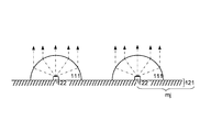
- a lens 111 that transmits light from the LED 122 mounted on the mounting board 121 is attached (a module including the mounting board 121, the LED 122, and the lens 111 is installed). Referred to as light emitting module mj).
- the light shown in FIG. 17 (see the dashed line arrow) is converged by the lens 111 and does not pass through the lens as shown in FIG. Proceed along.
- the brightness of the backlight from the backlight unit in the front view is improved.
- the circular image represents the light that has passed through the lens 111.
- the two-dot chain line circular image includes an image divided by a one-dot chain line circle, and the one-dot chain line circle includes an image divided by a dotted line circle.
- the difference in brightness is smaller so that the light from the backlight unit (backlight light) does not include unevenness in the amount of light.
- the region ar1 having the highest luminance lm1 is preferably as narrow as possible in the region (ar1 + ar2 + ar3) indicating the light that has passed through the lens 111 (however, this is 1 for suppressing unevenness in the amount of light). Only one metric and of course there are other metrics).
- the ratio ro derived from ar1 / (ar1 + ar2 + ar3) is about 47% and cannot be said to be small. That is, in the backlight unit that uses light passing through the hemispherical lens 111, the luminance in the front view is improved, but unevenness in the amount of light cannot be prevented (in short, the light emitting module mj including the hemispherical lens 111 has unevenness in the amount of light. ), And the backlight unit on which it is mounted also emits backlight light including unevenness in the amount of light).
- the present invention has been made to solve the above problems. And the objective is to provide the light emitting module etc. which emit the light which suppressed the light quantity nonuniformity.
- the light emitting module includes a light emitting element and a lens that transmits light from the optical element. And in this light emitting module, a depression hole is formed in the location which overlaps with a light emitting element on the output surface of a lens, and also the following formula
- the light from the light emitting element is guided in the radiation direction around the depression hole by the lens surface surrounding the depression hole.
- the curved surface of the lens surface surrounding the depression hole has a stronger curvature than, for example, the curved surface of the lens surface without the depression hole, so that the light of the light emitting element is diverged without being collected in the vicinity of the depression hole. Therefore, this light emitting module emits light having uniform luminance as a whole without excessively increasing the luminance directly above the light emitting element (in short, the light emitting module emits light with suppressed light amount unevenness).
- the curved surface of the lens surface surrounding the depression hole diverges without collecting light of the light emitting element in the vicinity of the depression hole and without excessively deviating from the depression hole. Let Therefore, the light emitting module surely emits light having uniform brightness as a whole.
- the material of the lens is not particularly limited, but is preferably a material satisfying the following formula (2). 1.49 ⁇ nd ⁇ 1.50 Formula (2) However, nd: the refractive index of the lens material.
- the lens is a diffusion lens.
- the light transmitted through the diffusing lens diffuses, and thus the light from the light emitting module is less likely to include light amount unevenness.
- the back surface of the lens surface be a Lambertian scattering surface.
- the Lambert scattering surface is preferably a textured surface or a coating surface coated with scattering particles.
- the light emitting module emits light from the light emitting element without losing light from the lens surface. Overall brightness) is increased.
- the second reflecting sheet is disposed between the lenses and the reflectance of the second reflecting sheet is 97% or more. If it is in this way, it will become difficult for the light from a light emitting module to contain the dark part corresponding between lenses, and it will become difficult to contain light quantity nonuniformity in the light from the illuminating device.
- a display device including a lighting device and a display panel (for example, a liquid crystal display panel) that receives light from the lighting device can produce a high-quality image without unevenness in light amount due to an increase in illuminance of the lighting device.
- a display panel for example, a liquid crystal display panel
- a television receiver is an example of a device on which such a display device is mounted.
- the light emitting module of the present invention emits light having uniform brightness as a whole by preventing light from being collected in the vicinity of the light emitting element. That is, this light emitting module emits light with suppressed light amount unevenness.
- FIG. 3 is an exploded perspective view of an LED module.
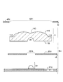
- FIG. 4 is an exploded cross-sectional view of the LED module (note that the cross-sectional direction is the direction of the arrow A1-A1 ′ in FIG. 1).
- FIG. 2 is a schematic perspective view of a simulation apparatus. Is an image showing a luminance distribution of light emitted through two lenses. These are graphs of a luminance distribution in which the vertical axis represents luminance [cd / m2] and the horizontal axis represents a position (a position where the middle of two lenses arranged between them is “0”).
- FIG. 1 is an exploded perspective view of an LED module.
- FIG. 4 is an exploded cross-sectional view of the LED module (note that the cross-sectional direction is the direction of the arrow A1-A1 ′ in FIG. 1).
- FIG. 2 is a schematic perspective view of a simulation apparatus. Is an image showing a luminance distribution of light emitted through two lenses. These are graphs
- FIG. 5 is a graph of a luminance distribution in which the vertical axis is normalized density and the horizontal axis is a position by normalizing the highest luminance shown in FIG. 5 as “1.0”.
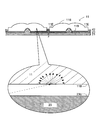
- FIG. 4 is an optical path diagram showing light transmitted through a lens.
- FIG. 4 is an optical path diagram showing light transmitted through a lens.
- Is an image showing the luminance distribution of light emitted through two lenses (curvature radius R 10 mm).
- Is an image showing a luminance distribution of light emitted through two lenses (curvature radius R 7.5 mm).
- FIG. 3 is an exploded perspective view of an LED module.
- FIG. 3 is an exploded perspective view of an LED module.
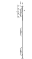
- FIG. 4 is an exploded cross-sectional view of the LED module (note that the cross-sectional direction is the direction of arrow A2-A2 ′ in FIG. 10). These are side views of an LED module.
- FIG. 4 is an optical path diagram showing scattering on the back surface of the lens. These are explanatory drawings which contrasted the position of a lens and the brightness
- FIG. 3 is an exploded perspective view of a liquid crystal display device. These are the exploded perspective views of the liquid crystal television which mounts a liquid crystal display device. These are the optical-path diagrams of the LED module mounted in the conventional backlight unit. These are the optical-path diagrams of LED mounted in the conventional backlight unit. These are images showing the luminance distribution of the light emitted through the two lenses in FIG.
- FIG. 16 shows a liquid crystal television 89 equipped with a liquid crystal display device (display device) 69.
- a liquid crystal television 89 can be said to be a television receiver because it receives a television broadcast signal and projects an image.
- FIG. 15 is an exploded perspective view showing the liquid crystal display device.
- a liquid crystal display device 69 includes a liquid crystal display panel 59, a backlight unit (illumination device) 49 that supplies light to the liquid crystal display panel 59, and a housing HG (front housing HG1) that sandwiches them. -Back housing HG2).
- an active matrix substrate 51 including a switching element such as a TFT (Thin Film Transistor) and a counter substrate 52 facing the active matrix substrate 51 are bonded together with a sealant (not shown). Then, liquid crystal (not shown) is injected into the gap between the substrates 51 and 52.
- a switching element such as a TFT (Thin Film Transistor)
- a counter substrate 52 facing the active matrix substrate 51 are bonded together with a sealant (not shown). Then, liquid crystal (not shown) is injected into the gap between the substrates 51 and 52.
- a polarizing film 53 is attached to the light receiving surface side of the active matrix substrate 51 and the emission side of the counter substrate 52.
- the liquid crystal display panel 59 as described above displays an image using the change in transmittance caused by the inclination of the liquid crystal molecules.
- the backlight unit 49 includes an LED module (light emitting module) MJ, a backlight chassis 41, a large reflective sheet 42, a diffusion plate 43, a prism sheet 44, and a microlens sheet 45.
- LED module light emitting module
- the backlight unit 49 includes an LED module (light emitting module) MJ, a backlight chassis 41, a large reflective sheet 42, a diffusion plate 43, a prism sheet 44, and a microlens sheet 45.
- the LED module MJ includes a mounting substrate 21, an LED (Light Emitting Diode) 22, The lens 11 and the built-in reflection sheet 23 are included.
- the mounting substrate 21 is a plate-shaped and rectangular substrate, and a plurality of electrodes (not shown) are arranged on the mounting surface 21U. And LED22 which is a light emitting element is attached on these electrodes.
- a resist film (not shown) serving as a protective film is formed on the mounting surface 21U of the mounting substrate 21.
- the resist film is not particularly limited, but is desirably white having reflectivity. This is because even if light is incident on the resist film, the light is reflected by the resist film and tends to go outside, thereby eliminating the cause of unevenness in the amount of light due to light absorption by the mounting substrate 21.
- the LED 22 is a light source and emits light by a current through the electrodes of the mounting substrate 21. And there are many kinds of LED22, and the following LED22 is mentioned.
- the LED 22 includes a blue light emitting LED chip (light emitting chip) and a phosphor that receives light from the LED chip and fluoresces yellow light (the number of LED chips is the same). Not particularly limited).
- Such an LED 22 generates white light by the light from the LED chip emitting blue light and the light emitting fluorescence.
- the phosphor incorporated in the LED 22 is not limited to a phosphor that emits yellow light.
- the LED 22 includes a blue light emitting LED chip and a fluorescent material that receives light from the LED chip and emits green light and red light, and emits blue light and fluorescent light emitted from the LED chip ( White light may be generated with green light and red light.
- the LED chip built in the LED 22 is not limited to a blue light emitting device.
- the LED 22 may include a red LED chip that emits red light, a blue LED chip that emits blue light, and a phosphor that emits green light by receiving light from the blue LED chip. This is because such an LED 22 can generate white light from red light from the red LED chip, blue light from the blue LED chip, and green light that emits fluorescence.
- the LED 22 may not include any phosphor.
- the LED 22 may include a red LED chip that emits red light, a green LED chip that emits green light, and a blue LED chip that emits blue light, and generates white light using light from all the LED chips.
- a relatively long mounting board 21 mounted in a row is mounted.
- the two types of mounting boards 21 are arranged such that a row of five LEDs 22 and a row of eight LEDs 22 are arranged to form a row of 13 LEDs 22, and further, with respect to the direction in which the 13 LEDs 22 are arranged.
- the two types of mounting boards 21 are also arranged in the crossing (orthogonal) direction.
- the LEDs 22 are arranged in a matrix and emits planar light (for convenience, the direction in which different types of mounting boards 21 are arranged is defined as the X direction, and the direction in which the same type of mounting boards 21 are arranged is defined as the Y direction.
- the direction intersecting with the Z direction is defined as Z).
- the thirteen LEDs 22 arranged in the X direction are electrically connected in series, and the thirteen LEDs 22 connected in series are connected to another thirteen LEDs 22 connected in series along the Y direction. Electrically connected in parallel.
- the LEDs 22 arranged in a matrix are driven in parallel.
- the lens 11 receives light from the LED 22 and transmits (emits) the light. More specifically, the lens 11 has an accommodation recess DH that can accommodate the LED 22 on the back surface (light-receiving surface) side of the lens surface 11 ⁇ / b> S, and covers the LED 22 while aligning the position of the accommodation recess DH with the LED 22. Then, the LED 22 is embedded in the lens 11, and the light from the LED 22 is reliably supplied into the lens 11. Then, most of the supplied light is emitted to the outside through the lens surface 11S ⁇ the details of the lens surface (emission surface) 11S will be described later ⁇ .
- the material used as the lens 11 is not specifically limited,
- an acrylic resin is mentioned (an acrylic resin whose refractive index nd is 1.49 or more and 1.50 or less is mentioned).
- the built-in reflection sheet 23 is interposed between the lens 11 and the mounting substrate 21.
- the built-in reflection sheet 23 prevents the mounting surface 21U of the mounting substrate 21 from being exposed through the passage opening 42H for allowing the lens 11 formed on the large-format reflection sheet 42 to pass therethrough.
- the large reflective sheet 42 includes a passage opening 42H that is larger than the outer diameter of the lens 11 in order to expose the lens 11 to its reflective surface 42U. Then, when the lens 11 is exposed on the reflection surface 42U of the large-format reflection sheet 42, a gap is generated between the outer edge 11E of the lens 11 and the inner edge of the passage opening 42H, and the mounting surface 21U of the mounting substrate 21 is formed from the gap. There is a risk of exposure. Therefore, the built-in reflection sheet 23 has a shape that borders the outer edge 11E of the lens 11, for example, a ring shape as shown in FIG.
- the built-in reflective sheet 23 shown in FIG. 1 is not a series of rings, but has a cut ST.
- This cut ST is for attaching the built-in reflection sheet 23 near the outer edge 11E of the lens 11 even after the mounting substrate 21 and the lens 11 are attached.
- the cut ST is not essential.
- the built-in reflecting sheet 23 is interposed between the lens 11 and the mounting substrate 21 in advance.
- the reflection surface of the built-in reflection sheet 23 is referred to as a built-in reflection surface 23U).
- the backlight chassis 41 is, for example, a box-shaped member, and houses the plurality of LED modules MJ by spreading the LED modules MJ on the bottom surface 41 ⁇ / b> B.
- the bottom surface 41B of the backlight chassis 41 and the mounting substrate 21 of the LED module MJ are connected via a rivet (not shown).
- a support pin that supports a later-described diffuser plate 43, prism sheet 44, and microlens sheet 45 may be attached to the bottom surface 41B of the backlight chassis 41 (note that the backlight chassis 41 has side walls along with the support pins).
- the diffusion plate 43, the prism sheet 44, and the microlens sheet 45 may be stacked and supported in this order).
- the large reflective sheet 42 is an optical sheet having a reflective surface 42U, and covers the plurality of LED modules MJ arranged in a matrix with the back surface of the reflective surface 42U facing.
- the large reflective sheet 42 includes a through hole 42H that matches the position of the lens 11 of the LED module MJ, and exposes the lens 11 from the reflective surface 42U (note that the above-described rivets and support pins are not exposed). There should be holes).
- the light emitted from the lens 11 travels toward the bottom surface 41B side of the backlight chassis 41, it is reflected by the reflecting surface 42U of the large reflective sheet 42 and travels away from the bottom surface 41B. To do. Accordingly, the presence of the large reflective sheet 42 causes the light of the LED 22 to travel toward the diffusion plate 43 facing the reflective surface 42U without loss.
- the diffusion plate 43 is an optical sheet that overlaps the large reflective sheet 42, and diffuses the light emitted from the LED module MJ and the reflected light from the large reflective sheet 42U. That is, the diffusing plate 43 diffuses the planar light formed by the plurality of LED modules MJ and spreads the light over the entire liquid crystal display panel 59.
- the diffusion plate 43 preferably has a transmittance of 52% or more and 60% or less. This is because such a diffusing plate 43 can diffuse while appropriately transmitting light and suppress unevenness in the amount of light.
- the prism sheet 44 is an optical sheet that overlaps the diffusion plate 43.
- the prism sheet 44 arranges, for example, triangular prisms extending in one direction (linear) in a direction intersecting with one direction in the sheet surface. Thereby, the prism sheet 44 deflects the radiation characteristic of the light from the diffusion plate 43.
- the prisms extend along the Y direction with a small number of LEDs 22 arranged, and are arranged along the X direction with a large number of LEDs 22 arranged.
- the microlens sheet 45 is an optical sheet that overlaps the prism sheet 44.
- the microlens sheet 45 disperses the fine particles that refract and scatter light inside. As a result, the microlens sheet 45 suppresses the light / dark difference (light intensity unevenness) without locally condensing the light from the prism sheet 44.
- the backlight unit 49 as described above supplies the planar light formed by the plurality of LED modules MJ through the plurality of optical sheets 43 to 45 to the liquid crystal display panel 59.
- the non-light-emitting liquid crystal display panel 59 receives the light (backlight light) from the backlight unit 49 and improves the display function.
- FIG. 3 is a schematic diagram of the simulation device 79.
- This simulation device 79 includes an experimental unit 71 and a photographing camera 73.
- the experimental unit 71 has an LED module MJ including two lenses 11 in a box 72 including an opening and a reflecting surface having a reflectance of about 97% on the bottom surface, a reflecting surface having a reflectance of approximately 100% on the inner wall. Is installed. Furthermore, the experiment unit 71 arranges the diffusion plate 43 in the opening of the box 72, thereby allowing the light from the LED module MJ to pass through the diffusion plate 43.
- the photographing camera 73 measures the luminance on the surface of the diffusion plate 43 by photographing the diffusion plate 43. Specifically, as shown in FIG. 4, an image that can identify the brightness level for each area in two dimensions is taken.
- an image showing two circles is obtained by the photographing camera 73.
- This circular image represents the light that has passed through the lens 11.
- the two-dot chain line circular image includes an image divided by a one-dot chain line circle, and the one-dot chain line circle includes an image divided by a dotted line circle.
- the image of FIG. 4 includes a plurality of ranges according to luminance. Therefore, the area surrounded only by the dotted line is AR1, the area surrounded by the dotted line and the alternate long and short dash line is AR2, and the area surrounded by the alternate long and short dashed line is not surrounded by AR3, the dotted line, the alternate long and short dashed line
- the other area is AR4.
- the luminance [cd / m2] of these areas AR1, AR2, AR3, AR4 is LM1, LM2, LM3, LM4, the relationship between them is LM1> LM2> LM3> LM4 (note that the highest luminance is obtained).
- LM1, LM2, LM3, and LM4 are normalized by values, LM1> 66%, 50% ⁇ LM2 ⁇ 66%, 30% ⁇ LM3 ⁇ 50%, and LM4 ⁇ 30%).
- the area AR1 having the highest luminance LM1 is preferably as narrow as possible in the area (AR1 + AR2 + AR3) indicating the light that has passed through the lens 11 (however, this is not the light intensity unevenness). It is only one index for suppressing the above, and other indexes naturally exist).
- the lens 11 has a part of the lens surface 11S that overlaps the housing recess DH (that is, the LED 22). It includes the depressed hole 11D.
- FIG. 5 shows a graph indicated by “0”. Further, by normalizing the highest luminance shown in FIG. 5 as “1.0”, a graph with the vertical axis as the normalized density and the horizontal axis as the position is shown in FIG.
- the position of the white arrow in FIGS. 5 and 6 is the position of the LED 22. Based on FIGS. 4 to 6, the following equation (P1) is obtained.
- R radius of curvature [unit: mm] of the curved surface from the recessed hole 11D to the outer edge 11E of the lens surface 11S It is.
- the light (B1 to B5) from the center of the lens surface 11S to the outer edge 11E is emitted radially without deviation as shown in the schematic diagram of the optical path of FIG. 7A (note that the light B1 is This means light passing through the vicinity of the depression hole 11D on the lens surface 11S, and the light passing through the part approaching the outer edge 11E of the lens surface 11S as the number assigned to the light B increases.
- the converged light other than the light passing through the depression 11D may have a higher luminance than the light B1 passing through the depression 11D.
- the light emitted from the lens 11 has a ring shape, and a luminance difference occurs between the center of the ring and the ring itself, and this luminance difference can cause unevenness in the amount of light.
- the radius of curvature R is, for example, greater than 13 [mm] (13 ⁇ R)
- the light convergence due to the curved surface is excessively lowered as shown in FIG. 7C.
- the light B2 close to the light B1 cannot be refracted so as to deviate from the light B1.
- the luminance difference between the vicinity of the LED 22 and the vicinity of the LED 22 becomes larger than in the case of other curvature radii R, and unevenness in the amount of light occurs. Therefore, in the lens 11 having the curvature R exceeding the upper limit value of the formula (P1), the light amount unevenness is not eliminated.
- the lens 11 can be said to be a diffusing lens). That is, the light from the LED 22 covered with the depression hole 11D is guided in a radiation direction centered on the depression hole 11D by the lens surface 11S surrounding the depression hole 11D.
- the curved surface of the lens surface 11S surrounding the depression hole 11D does not collect the light of the LED 22 near the depression hole 11D and from the depression hole 11D. Diversify without excessive separation (see FIG. 7A). Therefore, the LED module MJ emits light having uniform brightness as a whole without excessively increasing the brightness directly above the LED 22 (in short, the LED module MJ emits light with suppressed light amount unevenness).
- the light guide plate is omitted, and the LED directly enters the optical sheet (diffuser plate, etc.).
- the optical sheet diffuser plate, etc.
- the distance from the LED to the diffusion plate should be long.
- the lens 11 including the lens surface 11S having the depression 11D covers each LED 22, the light from the LED 22 is sufficiently diffused before reaching the diffusion plate 43.
- Backlight does not include unevenness in the amount of light.
- the distance between the LED 22 and the diffusion plate 43 may be relatively short (in short, the backlight unit 49 is relatively thin, and the liquid crystal display device 69 on which the backlight unit 49 is mounted is also likely to be thin).
- the driving heat of the LED 22 tends to be confined in a narrow space called the accommodation recess DH of the lens 11 (and the LED 22 cannot maintain a relatively high light intensity due to its own driving heat).
- the LED module MJ is attached to the backlight chassis 41 formed of a material with high heat dissipation, for example, metal.
- a separate heat dissipation member is not required between the mounting substrate 21 and the bottom surface 41B of the backlight chassis 41. Therefore, the backlight unit 49 capable of maintaining the light intensity over a long period of time at a low cost is completed.
- FIGS. 10 is a partial perspective view of the LED module MJ
- FIG. 11 is a cross-sectional view taken along line A2-A2 'of FIG.
- FIG. 12 is a partial side view of the LED module MJ (in FIG. 12, the built-in reflective sheet 23 and the large reflective sheet 42 are omitted for convenience).
- the leg portion 11F of the lens 11 is formed so as to protrude from the back surface 11B of the lens surface 11S.
- the built-in reflection sheet 23 includes leg openings 23HF for allowing the legs 11F of the lens 11 to pass therethrough so as not to hinder the connection between the lens 11 covering the lens 11 and the mounting substrate 21. That is, the built-in reflection sheet 23 is covered with the lens 11 and is interposed between the lens 11 and the mounting substrate 21 (of course, the built-in reflection sheet 23 is used for exposing the LED 22 to the built-in reflection surface 23U. Since the LED opening 23HL is included, the light from the LED 22 is not blocked).
- the lens 11 is attached to the mounting substrate 21 by the close contact between the tip of the leg 11F and the mounting surface 21U of the mounting substrate 21.
- a gap is generated between the mounting surface 21U and the lens 11 (specifically, a gap is generated between the back surface 11B of the lens 11 and the mounting surface 21U of the mounting substrate 21). Then, even if the LED 22 is heated for light emission, the heat is cooled through the gap.
- the outside air enters the housing recess DH that houses the LED 22 through the gap, and the heat generated by the LED 22 is easily escaped (in short, the leg portion 11F of the lens 11 causes the rear surface 11B of the lens 11 and the mounting surface 21U to escape).
- the gap is generated, the driving heat of the LED 22 is easily escaped outside without being confined in the narrow space DH of the lens 11).
- the junction temperature of the LED 22 does not become high, and the LED 22 emits light without reducing the luminance.
- the built-in reflection sheet 23 is circular, and the built-in reflection surface 23 ⁇ / b> U is covered with the back surface 11 ⁇ / b> B of the lens 11. Therefore, in this LED module MJ, the light reflected by the back surface 11B of the lens 11 is not absorbed by, for example, the mounting surface 21U or reflected by the mounting surface 21U and does not enter the back surface 11B of the lens 11. . That is, the light from the LED 22 is emitted through the lens 11 without loss. As a result, the light emitted from the LED module MJ is less likely to include light amount unevenness.
- such a built-in reflective surface 23U may be a mirror surface (also referred to as a Gaussian scattering surface) or a rough surface (also referred to as a Lambertian scattering surface) formed by embossing or the like.
- the built-in reflective surface 23U for Lambert scattering includes a texture pattern, but the method of forming the texture pattern (texture processing) is not particularly limited.
- the embossed pattern may be formed by various methods such as masking, roll transfer, or extrusion.
- beads that scatter light may be coated on the built-in reflective surface 23U. That is, it is sufficient that Lambertian scattering is generated even if the built-in reflective surface 23U is a coated surface coated with beads.
- the surface roughness [Ra] of the built-in reflective surface 23U having such a rough surface is 400 nm or more.
- a rough surface formed by embossing or the like may be formed on the back surface 11B of the lens 11. In this case, the light incident directly on the back surface 11B of the lens 11 is scattered from the LED 22.
- the light of the LED 22 is reliably emitted through the lens 11 without loss, and the illuminance of the entire illuminance range by the LED module MJ is further increased.
- Such a scattering state has been confirmed as a relatively good result by verification using, for example, optical analysis software SPEOS manufactured by OPTIS ⁇ Asia & Pacific.
- the large-format reflective sheet 42 has a reflectance of 97% or more.
- the luminance in the vicinity immediately above the lens 11 corresponds to the luminance in the vicinity immediately above the lens 11. Compared to, it will not be too low.
- the luminance curve Lp indicates the luminance of light from the LED module MJ covered by the large-format reflection sheet 42 having a reflectance of 97%.
- the luminance curve Lc indicates the luminance of light from the LED module MJ when the large-format reflection sheet 42 is not covered (note that the maximum luminance in the luminance curves Lp and Lc is approximately the same). Then, as can be seen from the luminance curve Lc and the luminance curve Lp in FIG. 14, the difference between the luminance near the lens 11 on the luminance curve Lp and the luminance near the lens 11 between the lenses 11 is the lens on the luminance curve Lc. 11 is smaller than the difference between the brightness near the top of 11 and the brightness near the top between the lenses 11.
- the magnitude of the luminance difference indicates whether or not the light from the backlight unit 49 includes light amount unevenness (in short, the light amount unevenness occurs when the luminance difference is large). Then, the light from the backlight unit 49 on which the LED module MJ when not covering the large-format reflection sheet 42 includes light amount unevenness, but the LED covered with the large-format reflection sheet 42 having a reflectivity of 97%. The light from the backlight unit 49 on which the module MJ is mounted does not include light amount unevenness. That is, it can be said that it is desirable that the large-size reflection sheet 42 having a reflectance of 97% is mounted on the backlight unit 49.
- the LED 22 which is a light emitting element is used as the light source.
- the present invention is not limited to this.
- it may be a light emitting element formed of a self-luminous material such as organic EL (Electro-Luminescence) or inorganic EL.
- the acrylic resin is taken as an example of the material of the lens 11.
- the material is not limited to this, and other transparent resin may be used.
- the lens 11 having a curved surface satisfying the formula (P1) is designed based on a material having a refractive index nd of about 1.49 or more and 1.50 or less, it can be said that an acrylic resin is desirable. However, even if the refractive index is nd, the formula (P1) may be satisfied, so that other transparent resin or glass may be used.
Landscapes
- Physics & Mathematics (AREA)
- General Physics & Mathematics (AREA)
- Optics & Photonics (AREA)
- Nonlinear Science (AREA)
- Mathematical Physics (AREA)
- Chemical & Material Sciences (AREA)
- Crystallography & Structural Chemistry (AREA)
- Engineering & Computer Science (AREA)
- General Engineering & Computer Science (AREA)
- Planar Illumination Modules (AREA)
- Liquid Crystal (AREA)
Abstract
LEDモジュール(MJ)は、LED(22)と、そのLED(22)からの光を透過させるレンズ(11)と、を含む。そして、このLEDモジュール(MJ)では、レンズ(11)のレンズ面(11S)で、LED(22)に重なる箇所に、陥没孔(11D)が形成され、さらに、所定の式が満たされる。
Description
本発明は、発光素子のような光源を含んだ発光モジュール、その発光モジュールを採用する照明装置、その照明装置を搭載する表示装置、さらには、表示装置を搭載するテレビ受像装置に関する。
非発光型の液晶表示パネル(表示パネル)を搭載する液晶表示装置(表示装置)では、通常、その液晶表示パネルに対して、光を供給するバックライトユニット(照明装置)も搭載される。バックライトユニットにおける光源には、種々の種類が存在する。例えば、特許文献1に示されるバックライトユニットの場合、光源はLED(Light Emitting Diode)である。
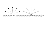
さらに、このバックライトユニットでは、図17に示すように、実装基板121に実装されたLED122からの光を透過させるレンズ111が取り付けられる(なお、実装基板121、LED122、およびレンズ111を含むモジュールを発光モジュールmjと称する)。このようになっていると、図17に示す光(一点鎖線矢印参照)は、レンズ111によって収斂され、図18に示すようなレンズを通過することなく、出射するLED122の光に比べ、鉛直方向に沿うように進む。これによって、バックライトユニットからのバックライト光の正面視の輝度が向上する。
ところで、撮影カメラで、図17に示すような2つのLED122の正面からの輝度を撮影すると、図19に示すような画像が得られる(なお、この撮影では、撮影カメラとレンズ111との間に拡散板が介在し、その拡散板を撮影している)。
この画像では、円形の画像はレンズ111を経た光を表す。そして、この二点鎖線の円形画像の内部には、一点鎖線の円形で区分けされる画像が含まれ、さらに、その一点鎖線の円形の内部には点線の円形で区分けされる画像が含まれる。
これらの円形の線は、高低差のある輝度範囲の境界線を示す。すると、図19の画像は、輝度に応じた複数の範囲を含む。そこで、点線のみで囲まれる領域をar1、点線と一点鎖線とで囲まれる領域をar2、一点鎖線と二点鎖線とで囲まれる領域をar3、点線、一点鎖線、二点鎖線で囲まれていないその他の領域をar4とする。そして、これら領域ar1、ar2、ar3、a4の輝度[cd/m2]を、lm1、lm2、lm3、lm4とすると、それらの関係は、lm1>lm2>lm3>lm4となる。
通常、バックライトユニットからの光(バックライト光)に、光量ムラが含まれないようにするには、輝度の高低差が小さいほどよい。すると、図18の画像にて、最も高い輝度lm1の領域ar1が、レンズ111を経た光を示す領域(ar1+ar2+ar3にて、極力狭いほどよいといえる(ただし、これは、光量ムラを抑えるための1つの指標にすぎず、当然、その他の指標も存在する)。
しかしながら、図19の画像から明らかなように、ar1/(ar1+ar2+ar3)から導き出される比率roは、47%程度であり、小さいとはいえない。つまり、半球状のレンズ111を通過する光を用いるバックライトユニットでは、正面視の輝度は向上するものの、光量ムラを防止できない(要は、半球状のレンズ111を含む発光モジュールmjは、光量ムラを含む光を発しており、それを搭載するバックライトユニットも光量ムラを含むバックライト光を発する)。
本発明は、上記の問題点を解決するためになされたものである。そして、その目的は、光量ムラを抑制させた光を発する発光モジュール等を提供することにある。
発光モジュールは、発光素子と、その光素子からの光を透過させるレンズと、を含む。そして、この発光モジュールでは、レンズの出射面で、発光素子に重なる箇所に、陥没孔が形成され、さらに、以下の式(1)が満たされる。
8≦R≦13 … 式(1)
ただし、
R:陥没孔から出射面の外縁に至るまでの曲面が有する曲率半径[単位
;mm]
である。
8≦R≦13 … 式(1)
ただし、
R:陥没孔から出射面の外縁に至るまでの曲面が有する曲率半径[単位
;mm]
である。
このようになっていると、発光素子からの光は、陥没孔を囲むレンズ面によって、陥没孔を中心とする放射方向に導かれる。特に、この陥没孔を囲むレンズ面の曲面は、例えば陥没孔の無いレンズ面の曲面に比べて、強い曲率を有するので、発光素子の光を陥没孔の直上付近に集めることなく発散させる。そのため、この発光モジュールは、発光素子の直上の輝度を過剰に高くせずに、全体として均一な輝度を有する光を発する(要は、発光モジュールは光量ムラを抑えた光を発する)。
その上、式(1)が満たされれば、この陥没孔を囲むレンズ面の曲面は、発光素子の光を陥没孔の直上付近に集めることなく、かつ、陥没孔から過剰に乖離させることなく発散させる。そのため、発光モジュールは、確実に、全体として均一な輝度を有する光を発する。
また、レンズの材料は特に限定されるものではないが、以下の式(2)を満たす材料であると望ましい。
1.49≦nd≦1.50 … 式(2)
ただし、
nd:レンズの材料が有する屈折率
である。
1.49≦nd≦1.50 … 式(2)
ただし、
nd:レンズの材料が有する屈折率
である。
また、レンズが、拡散レンズであると望ましい。このようになっていると、拡散レンズを透過する光は拡散するので、発光モジュールからの光に光量ムラが含まれにくくなる。
また、レンズ面の背面が、ランバート散乱面であると望ましい。このようになっていると、レンズ内部に入射する光が種々方向に進行する。そのため、レンズからの光に光量ムラが含まれにくい。
なお、ランバート散乱面は、シボ加工面または散乱粒子でコーティングされたコーティング面であると望ましい。
また、以上の発光モジュールを含む照明装置であれば、その発光モジュールが、発光素子からの光を損失させることなく、レンズ面から出射させるので、照明装置による照度範囲全体の照度(ひいては、輝度範囲全体の輝度)が高まる。
なお、このような照明装置では、レンズ同士の間には、第2反射シートが配置され、その第2反射シートの反射率が、97%以上であると望ましい。このようになっていると、発光モジュールからの光に、レンズ同士の間対応する暗部が含まれにくくなり、その照明装置からの光に光量ムラが含まれにくくなる。
さらに、照明装置と、その照明装置からの光を受ける表示パネル(例えば、液晶表示パネル)とを含む表示装置は、照明装置の照度の高まりに起因して、光量ムラのない高品質な画像を提供する(なお、このような表示装置を搭載する装置としては、テレビ受像装置が一例として挙げられる)。
本発明の発光モジュールによると、発光素子の直上付近に光を集めないようにすることで、全体として均一な輝度を有する光を発する。つまり、この発光モジュールは、光量ムラを抑制させた光を発する。
[実施の形態1]
実施の一形態について、図面に基づいて説明すれば、以下の通りである。なお、便宜上、ハッチングや部材符号等を省略する場合もあるが、かかる場合、他の図面を参照するものとする。
実施の一形態について、図面に基づいて説明すれば、以下の通りである。なお、便宜上、ハッチングや部材符号等を省略する場合もあるが、かかる場合、他の図面を参照するものとする。
図16は、液晶表示装置(表示装置)69を搭載する液晶テレビ89である。なお、このような液晶テレビ89は、テレビ放送信号を受信して画像を映すことから、テレビ受像装置といえる。図15は、液晶表示装置を示す分解斜視図である。この図に示すように、液晶表示装置69は、液晶表示パネル59と、この液晶表示パネル59に対して光を供給するバックライトユニット(照明装置)49と、これらを挟み込むハウジングHG(表ハウジングHG1・裏ハウジングHG2)と、を含む。
液晶表示パネル59は、TFT(Thin Film Transistor)等のスイッチング素子を含むアクティブマトリックス基板51と、このアクティブマトリックス基板51に対向する対向基板52とをシール材(不図示)で貼り合わせる。そして、両基板51・52の隙間に液晶(不図示)が注入される。
なお、アクティブマトリックス基板51の受光面側、対向基板52の出射側には、偏光フィルム53が取り付けられる。そして、以上のような液晶表示パネル59は、液晶分子の傾きに起因する透過率の変化を利用して、画像を表示する。
次に、液晶表示パネル59の直下に位置するバックライトユニット49について説明する。バックライトユニット49は、LEDモジュール(発光モジュール)MJ、バックライトシャーシ41、大判反射シート42、拡散板43、プリズムシート44、および、マイクロレンズシート45を含む。
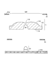
LEDモジュールMJは、図15の部分斜視図である図1、および、図1のA1-A1’線矢視断面である図2に示すように、実装基板21、LED(Light Emitting Diode)22、レンズ11、および内蔵反射シート23を含む。
実装基板21は、板状かつ矩形状の基板であり、実装面21U上に、複数の電極(不図示)を並べる。そして、これらの電極上に、発光素子であるLED22が取り付けられる。なお、実装基板21における実装面21Uには、保護膜となるレジスト膜(不図示)が成膜される。このレジスト膜は、特に限定されるものではないが、反射性を有する白色であると望ましい。なぜなら、レジスト膜に光が入射したとしても、その光はレジスト膜で反射して外部に向かおうとするので、実装基板21による光の吸収という光量ムラの原因が解消するためである。
LED22は、光源であり、実装基板21の電極を介した電流によって発光する。そして、LED22の種類は多々あり、以下のようなLED22が挙げられる。例えば、LED22は、青色発光のLEDチップ(発光チップ)と、そのLEDチップからの光を受けて、黄色光を蛍光発光する蛍光体と、を含むものが挙げられる(なお、LEDチップの個数は特に限定されない)。このようなLED22は、青色発光のLEDチップからの光と蛍光発光する光とで白色光を生成する。
ただし、LED22に内蔵される蛍光体は、黄色光を蛍光発光する蛍光体に限らない。例えば、LED22は、青色発光のLEDチップと、そのLEDチップからの光を受けて、緑色光および赤色光を蛍光発光する蛍光体と、を含み、LEDチップからの青色光と蛍光発光する光(緑色光・赤色光)とで白色光を生成してもよい。
また、LED22に内蔵されるLEDチップは、青色発光のものに限られない。例えば、LED22は、赤色発光の赤色LEDチップと、青色発光の青色LEDチップと、青色LEDチップからの光を受けて、緑色光を蛍光発光する蛍光体と、を含んでいてもよい。なぜなら、このようなLED22であれば、赤色LEDチップからの赤色光と、青色LEDチップからの青色光と、蛍光発光する緑色光とで白色光を生成できるためである。
また、全く蛍光体を含まないLED22であってもよい。例えば、赤色発光の赤色LEDチップと、緑色発光の緑色LEDチップと、青色発光の青色LEDチップと、を含み、全てのLEDチップからの光で白色光を生成するLED22であってもよい。
また、図15に示されるバックライトユニット49では、1枚の実装基板21に5個のLED22を列状に実装した比較的短い実装基板21と、1枚の実装基板21に8個のLED22を列状に実装した比較的長い実装基板21と、が搭載される。
特に、2種類の実装基板21は、5個のLED22の列と8個のLED22の列とを13個のLED22の列にするように並ばせ、さらに、13個のLED22の並ぶ方向に対して、交差(直交等)する方向にも、2種類の実装基板21は並ぶ。これにより、LED22はマトリックス状に配置され、面状光を発する(便宜上、異種の実装基板21の並ぶ方向をX方向、同種の実装基板21の並ぶ方向をY方向とし、このX方向とY方向とに交差する方向をZ方向とする)。
なお、X方向に並ぶ13個のLED22は、電気的に直列接続され、さらに、この直列につながった13個のLED22は、Y方向に沿って隣り合う別の13個の直列接続されたLED22と電気的に並列に接続される。そして、これらマトリックス状に並ぶLED22は、並列駆動される。
レンズ11は、LED22からの光を受け、その光を透過(出射)させる。詳説すると、レンズ11は、レンズ面11Sの背面(受光面)側にLED22を収容可能な収容窪みDHを有し、その収容窪みDHとLED22との位置を合わせつつ、LED22に覆い被さる。すると、レンズ11の内部に、LED22が埋め込まれ、LED22からの光が、確実に、レンズ11内部に供給される。そして、その供給された光の大部分が、レンズ面11Sを介して外部に出射する{なお、レンズ面(出射面)11Sについての詳細は、後述する}。
なお、レンズ11となる材料は特に限定されるものではないが、例えば、アクリル樹脂が挙げられる(屈折率ndが1.49以上1.50以下のアクリル樹脂が挙げられる)。
内蔵反射シート23は、レンズ11と実装基板21との間に介在する。そして、この内蔵反射シート23は、大判反射シート42に形成されたレンズ11を通過させるための通過開孔42Hから実装基板21の実装面21Uの露出を防ぐ。
詳説すると、大判反射シート42は、レンズ11を自身の反射面42Uに露出させるために、レンズ11の外径よりも大きな通過開孔42Hを含む。すると、レンズ11が大判反射シート42の反射面42Uに露出した場合、レンズ11の外縁11Eと通過開孔42Hの内縁との間に隙間が生じ、その隙間から、実装基板21の実装面21Uが露出するおそれがある。そこで、内蔵反射シート23は、レンズ11の外縁11Eを縁取るような形、例えば図1に示すような輪状を有する。
なお、この図1に示される内蔵反射シート23は、一連状の輪ではなく、切れ込みSTが形成されている。この切れ込みSTは、実装基板21とレンズ11との取り付け後であっても、内蔵反射シート23をレンズ11の外縁11E付近に取り付けるためのものである。ただし、切れ込みSTは必須ではない。
例えば、一連状かつ輪状の内蔵反射シート23であっても、実装基板21に対してレンズ11が取り付けられる場合に、そのレンズ11と実装基板21との間に、予め内蔵反射シート23が介在するようにすればよい(なお、内蔵反射シート23の反射面を内蔵反射面23Uとする)。
バックライトシャーシ41は、図15に示すように、例えば箱状の部材で、底面41BにLEDモジュールMJを敷き詰めることで、それら複数のLEDモジュールMJを収容する。なお、バックライトシャーシ41の底面41BとLEDモジュールMJの実装基板21とは、不図示のリベットを介して接続される。
また、バックライトシャーシ41の底面41Bには、後述の拡散板43、プリズムシート44、マイクロレンズシート45を支える支持ピンが取り付けられてもよい(なお、バックライトシャーシ41は、支持ピンとともに、側壁の頂きで、拡散板43、プリズムシート44、マイクロレンズシート45をこの順で積み重ねて支えてもよい)。
大判反射シート42は、反射面42Uを有する光学シートで、マトリックス配置された複数のLEDモジュールMJに、反射面42Uの裏面を向けて覆い被さる。ただし、大判反射シート42は、LEDモジュールMJのレンズ11の位置に合わせた通過開孔42Hを含み、反射面42Uからレンズ11を露出させる(なお、上述のリベットおよび支持ピンを露出させるための開孔があるとよい)。
すると、レンズ11から出射する光の一部が、バックライトシャーシ41の底面41B側に向かって進行したとしても、大判反射シート42の反射面42Uによって反射し、その底面41Bから乖離するように進行する。したがって、大判反射シート42が存在することで、LED22の光は損失することなく、反射面42Uに対向した拡散板43に向かう。
拡散板43は、大判反射シート42に重なる光学シートであり、LEDモジュールMJから発せられる光および大判反射シート42Uからの反射光を拡散させる。すなわち、拡散板43は、複数のLEDモジュールMJによって形成される面状光を拡散させて、液晶表示パネル59全域に光をいきわたらせる。なお、拡散板43は、52%以上60%以下の透過率を有していると望ましい。なぜなら、このような拡散板43であれば、光を適度に透過させつつ拡散でき、光量ムラを抑えられるためである。
プリズムシート44は、拡散板43に重なる光学シートである。そして、このプリズムシート44は、一方向(線状)に延びる例えば三角プリズムを、シート面内にて、一方向に交差する方向に並べる。これにより、プリズムシート44は、拡散板43からの光の放射特性を偏向させる。なお、プリズムは、LED22の配置個数の少ないY方向に沿って延び、LED22の配置個数の多いX方向に沿って並ぶとよい。
マイクロレンズシート45は、プリズムシート44に重なる光学シートである。そして、このマイクロレンズシート45は、光を屈折散乱させる微粒子を内部に分散させる。これにより、マイクロレンズシート45は、プリズムシート44からの光を、局所的に集光させることなく、明暗差(光量ムラ)を抑える。
そして、以上のようなバックライトユニット49は、複数のLEDモジュールMJによって形成される面状光を、複数枚の光学シート43~45を通過させ、液晶表示パネル59に供給する。これにより、非発光型の液晶表示パネル59は、バックライトユニット49からの光(バックライト光)を受光して表示機能を向上させる。
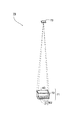
ここで、LEDモジュールMJにおけるレンズ11から発せられる光の輝度について詳説する。図3は、シミュレーション装置79の概略図である。このシミュレーション装置79は、実験ユニット71と撮影カメラ73とを含む。
実験ユニット71は、底面を97%程度の反射率を有する反射面、内壁をほぼ100%の反射率を有する反射面とし、さらに開口を含むボックス72に、2個のレンズ11を含むLEDモジュールMJを搭載する。さらに、実験ユニット71は、ボックス72の開口に拡散板43を配置させることで、その拡散板43にLEDモジュールMJからの光を透過させる。
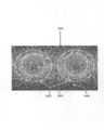
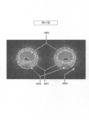
撮影カメラ73は、拡散板43を撮影することで、その拡散板43の面上の輝度を測定する。具体的には、図4に示すように、2次元で輝度の高低をエリア毎に識別可能な画像を撮影する。
この図4に示すように、2つの円形(二点鎖線の円形)を示す画像が撮影カメラ73によって得られる。この円形の画像はレンズ11を経た光を表す。そして、この二点鎖線の円形画像の内部には、一点鎖線の円形で区分けされる画像が含まれ、さらに、その一点鎖線の円形の内部には点線の円形で区分けされる画像が含まれる。
これらの円形の線は、高低差のある輝度範囲の境界線を示す。すると、図4の画像は、輝度に応じた複数の範囲を含む。そこで、点線のみで囲まれる領域をAR1、点線と一点鎖線とで囲まれる領域をAR2、一点鎖線と二点鎖線とで囲まれる領域をAR3、点線、一点鎖線、二点鎖線で囲まれていないその他の領域をAR4とする。そして、これら領域AR1、AR2、AR3、AR4の輝度[cd/m2]を、LM1、LM2、LM3、LM4とすると、それらの関係は、LM1>LM2>LM3>LM4となる(なお、輝度の最高値でLM1、LM2、LM3、LM4を規格化すると、LM1>66%、50%<LM2≦66%、30%<LM3≦50%、LM4≦30%である)。
通常、バックライトユニット49からの光(バックライト光)に、光量ムラが含まれないようにするには、輝度の高低差が小さいほどよい。すると、図4に示されるシミュレーションの結果にて、最も高い輝度LM1の領域AR1が、レンズ11を経た光を示す領域(AR1+AR2+AR3)にて、極力狭いほどよいといえる(ただし、これは、光量ムラを抑えるための1つの指標にすぎず、当然、その他の指標も存在する)。
そこで、AR1/(AR1+AR2+AR3)から導き出される比率ROを極力小さくするために、レンズ11は、図1および図2に示すように、収容窪みDH(すなわちLED22)に重なるレンズ面11Sの一部を陥没させた陥没孔11Dを含む。
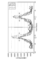
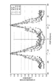
そして、このようなレンズ面11Sを透過する光に基づく輝度分布の画像(図4参照)を、縦軸を輝度[cd/m2]、横軸を位置(2つ並ぶレンズ11同士の中間を“0”とした位置)で示したグラフが図5になる。また、図5に示される最高輝度を“1.0”として規格化することで、縦軸を規格化濃度、横軸を位置にしたグラフが図6になる。なお、図5および図6における白色矢印の位置が、LED22の位置になる。そして、図4~図6を踏まえると、以下のような式(P1)が求められる。
8≦R≦13 … 式(P1)
ただし、
R:陥没孔11Dからレンズ面11Sの外縁11Eに至るまでの曲面が
有する曲率半径[単位;mm]
である。
ただし、
R:陥没孔11Dからレンズ面11Sの外縁11Eに至るまでの曲面が
有する曲率半径[単位;mm]
である。
曲率半径Rが式(P1)の範囲に収まる場合、図5および図6におけるR[mm]=8,10,12が該当する。そして、図5に示すように、式(P1)に収まる曲率半径Rの場合、その最高輝度は、他の曲率半径(R=7,15)の場合での最高輝度に比べて低い。
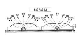
なぜなら、図7Aの光路概略図に示すように、レンズ面11Sの中心から外縁11Eに至るまでの光(B1~B5)は、偏ることなく放射状に出射するからである(なお、光B1が、レンズ面11Sにおける陥没孔11D付近を通過する光で、光Bに付す番号が大きくなるにつれて、陥没孔11Dから離れ、レンズ面11Sの外縁11Eに近づいた箇所を通過する光を意味する)。
特に、レンズ面11Sは、比較的光強度の強い光B2を最も光強度の強い光B1から乖離させる。したがって、最も高い輝度LM1を示す領域AR1の面積が小さくなりやすい(比率RO≒41%)。これは、曲率半径R=10(mm)を有するレンズ面11Sを経た光の画像を示す図8から明らかである。
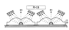
一方、曲率半径Rが、式(P1)の範囲外、例えば曲率半径Rが8[mm]未満の場合(R<8)、図7Bに示すように、曲面による光の収斂性が過剰に高まる。すると、陥没孔11Dを通過する光以外の光(光B2~光B5)が収斂する(図5における網斜線矢印参照)。そのため、図9の画像(R=7.5)に示すように、レンズ11を経た光を示す領域(AR1+AR2+AR3)が比較的小さくなる。
このように光が過剰に収斂し、レンズ11を経た光を示す領域が小さくなっていると、その光が拡散板43を経たとしても、十分に拡散されにくい(別表現すると、比率ROにおける分母が小さくなりやすく、その比率ROは小さくならない)。したがって、式(P1)の下限値を下回る曲率Rを有するレンズ11では、光量ムラが解消されない。
また、陥没孔11Dを通過する光以外(光B2~光B5)の収斂した光が、陥没孔11Dを通過する光B1よりも高い輝度を有することもあり得る。このような場合、レンズ11から出射する光は輪状になり、輪の中心と輪自体とで輝度差が生じ、この輝度差が光量ムラの原因になり得る。
次に、曲率半径Rが、例えば曲率半径Rが13[mm]を超える場合(13<R)、図7Cに示すように、曲面による光の収斂性が過剰に低下する。すると、陥没孔11Dを通過する光以外で、光B1に近い光B2が、光B1から乖離するように屈折進行できない。
そのため、図5および図6に示すように、LED22付近と、LED22から乖離した付近とでの輝度差が、その他の曲率半径Rの場合に比べて大きくなり、光量ムラが発生する。したがって、式(P1)の上限値を上回る曲率Rを有するレンズ11では、光量ムラが解消されない。
以上を踏まえると、レンズ11のレンズ面11Sに陥没孔11Dが形成されている場合、陥没孔11Dを境に分けられた曲面がレンズ面11Sに生じ、そのレンズ面11Sを通過する光は、全く陥没孔の無いレンズ面を通過する光に比べて、比較的光強度の強い光を一点に集中させない(図7Aに示す光B1・B2を参照)。
なぜなら、この陥没孔11Dを囲むレンズ面11Sの曲面は、陥没孔の無いレンズ面の曲面に比べて、強い曲率を有するので、LED22の光を陥没孔11Dの直上付近に集めることなく拡散させる(したがって、レンズ11は拡散レンズといえる)。すなわち、陥没孔11Dに覆われるLED22からの光は、陥没孔11Dを囲むレンズ面11Sによって、陥没孔11Dを中心とする放射方向に導かれる。
特に、式(P1)を満たすようなレンズ面11Sの場合、この陥没孔11Dを囲むレンズ面11Sの曲面は、LED22の光を陥没孔11Dの直上付近に集めることなく、かつ、陥没孔11Dから過剰に乖離させることなく発散させる(図7A参照)。そのため、このLEDモジュールMJは、LED22の直上の輝度を過剰に高くせずに、全体として均一な輝度を有する光を発する(要は、LEDモジュールMJは光量ムラを抑えた光を発する)。
したがって、このようなレンズ11を含むLEDモジュールMJは、光量ムラを抑制した光を出射し、それに起因して、バックライトユニット49からのバックライト光も光量ムラを含まない。また、LEDモジュールMJから出射する光自体が光量ムラを抑制されているので、バックライトユニット49に含む光量ムラ防止のための光学シートの枚数を減らしてもかまわない(要は、バックライトユニット49のコストが下がり、かつ、バックライトユニット49も薄型になる)。
[その他の実施の形態]
なお、本発明は上記の実施の形態に限定されず、本発明の趣旨を逸脱しない範囲で、種々の変更が可能である。
なお、本発明は上記の実施の形態に限定されず、本発明の趣旨を逸脱しない範囲で、種々の変更が可能である。
例えば、通常、直下型方式のバックライトユニットでは、導光板が省略され、LEDが、直接、光学シート(拡散板等)に光を入射させる。ただし、その光は光学シートに到達するまでにある程度発散しなければ、その光学シートを経て出射する場合に、光量ムラを含むことになる。したがって、LEDから拡散板までの距離は長い方がよい。
しかしながら、陥没孔11Dを有するレンズ面11Sを含んだレンズ11が、各々LED22を覆う場合、LED22からの光は、拡散板43に到達する前に、十分に拡散するので、バックライトユニット49からのバックライト光に光量ムラが含まれない。その上、LED22と拡散板43までの距離も比較的短くてよい(要は、比較的薄型なバックライトユニット49になり、それを搭載する液晶表示装置69も薄型になりやすい)。
ただし、図15に示すLEDモジュールMJが搭載されるバックライトユニット49では、多数のLED22が搭載され、さらに、各LED22は、レンズ11で覆われる。そのため、そのLED22の駆動熱は、レンズ11の収容窪みDHという狭空間にこもりやすい(ひいては、LED22が自身の駆動熱に起因して、比較的高い光強度を維持できない)。
そこで、LEDモジュールMJは、放熱性の高い材料、例えば金属で形成されたバックライトシャーシ41に取り付けられると望ましい。このようになっていると、例えば、実装基板21とバックライトシャーシ41の底面41Bとの間に、別個の放熱部材が不要になる。そのため、低コストでありながら、光強度を長時間にわたって維持できるバックライトユニット49が完成する。
また、LED22の駆動熱の放熱させる観点から、図10~図12に示すように、レンズ11に脚部11Fが形成されていると望ましい。図10はLEDモジュールMJの部分斜視図であり、図11は図10のA2-A2’線矢視断面である。また、図12はLEDモジュールMJの部分側面図である(図12では、内蔵反射シート23および大判反射シート42は、便宜上、省略する)。
これらの図に示すように、レンズ11の脚部11Fは、レンズ面11Sの背面11Bから突き出るように形成される。さらに、内蔵反射シート23は、自身に覆い被さるレンズ11と実装基板21との接続の障害にならないように、レンズ11の脚部11Fを通過させるための脚部用開孔23HFを含む。つまり、この内蔵反射シート23は、レンズ11に覆われることで、そのレンズ11と実装基板21との間に介在する(もちろん、内蔵反射シート23は、LED22を内蔵反射面23Uに露出させるためのLED用開孔23HLを含むので、LED22からの光を遮ることはない)。
そして、この脚部11Fの先端と実装基板21の実装面21Uとが密着することで、レンズ11が実装基板21に取り付けられる。
このようになっていると、実装面21Uとレンズ11との間に隙間が生じる(具体的には、レンズ11の背面11Bと実装基板21の実装面21Uとの間に隙間が生じる)。すると、LED22が発光のために熱を帯びたとしても、その熱が隙間を通じて冷やされる。
詳説すると、隙間を通じて、外気がLED22を収容する収容窪みDHに入り込み、LED22に帯びた熱が逃げやすくなる(要は、レンズ11の脚部11Fによって、レンズ11の背面11Bと実装面21Uとに隙間が生じると、LED22の駆動熱は、レンズ11の収容窪みDHという狭空間にこもらずに外部に逃げやすくなる)。この結果、LED22におけるジャンクション温度が高温にならず、そのLED22は輝度を低下させることなく発光する。
なお、図10および図11に示すように、内蔵反射シート23は円形で、内蔵反射面23Uはレンズ11の背面11Bに覆われる。そのため、このLEDモジュールMJでは、レンズ11の背面11Bで反射した光が、例えば実装面21Uに吸収されたり、実装面21Uで反射してレンズ11の背面11Bに入射しなかったり、ということにならない。つまり、LED22の光が損失することなくレンズ11を介して出射される。その結果、LEDモジュールMJから発せられる光に、光量ムラが含まれにくくなる。
なお、このような内蔵反射面23Uは、鏡面(ガウス散乱面ともいえる)であってもよいし、シボ加工等に形成される粗面(ランバート散乱面ともいえる)させるであってもかまわない。
また、ランバート散乱させる内蔵反射面23Uはシボパターンを含むが、そのシボパターンの形成(シボ加工)の方法は、特に限定されるわけではない。例えば、マスキング、ロール転写、または押し出し加工等の種々の方法で、シボパターンが形成されていてもよい。
また、シボ加工以外にも、光を散乱させるビーズ(散乱粒子)を、内蔵反射面23U上にコーティングしてもよい。つまり、内蔵反射面23Uがビーズでコーティングされたコーティング面であってもランバート散乱を生じさせるのであればよい。なお、このような粗面になった内蔵反射面23Uにおける面粗度[Ra]は、400nm以上である。
また、シボ加工等によって形成される粗面(ランバート散乱面)は、レンズ11の背面11Bに形成されていてもよい。このようになっていると、LED22から、直接、レンズ11の背面11Bに入射した光が散乱する。
そのため、その種々方向に散乱した光の一部が、内蔵反射シート23の内蔵反射面23Uに入射したとしても、ほとんどの光がレンズ11の背面11Bに戻って、レンズ11の内部に進入する。また、種々方向に拡散した光の別の一部は、図13の光路図に示すようにも進行する。すなわち、レンズ11の背面11Bに到達した光の一部(一点鎖線矢印)が、散乱しつつ、そのままレンズ11の内部に進入する。
その結果、LED22の光が損失することなくレンズ11を介して確実に出射し、LEDモジュールMJによる照度範囲全体の照度が一層高まる。なお、このような散乱状態は、例えば、(株)OPTIS Asia&Pacific社製の光学解析ソフトSPEOSを用いた検証で、比較的良好な結果として確認されている。
また、大判反射シート42は、97%以上の反射率を有していると望ましい。このようになっていると、レンズ11の位置と、輝度曲線Lp・Lcとを併記した図14に示すように、レンズ11の間に対応する直上付近の輝度が、レンズ11の直上付近の輝度に比べて、過度に低くならない。
詳説すると、輝度曲線Lpは、97%の反射率を有する大判反射シート42の被さったLEDモジュールMJからの光の輝度を示す。輝度曲線Lcは、大判反射シート42の被さっていない場合のLEDモジュールMJからの光の輝度を示す(なお、輝度曲線Lp・Lcにおける最高輝度はほぼ同値とする)。すると、図14の輝度曲線Lcと輝度曲線Lpとからわかるように、輝度曲線Lpにおけるレンズ11の直上付近の輝度とレンズ11同士の間の直上付近の輝度との差は、輝度曲線Lcにおけるレンズ11の直上付近の輝度とレンズ11同士の間の直上付近の輝度との差に比べて小さい。
このような輝度差の大小は、バックライトユニット49からの光に光量ムラが含まれるか否かを示す(要は、輝度差が大きいと、光量ムラが発生する)。すると、大判反射シート42の被さっていない場合のLEDモジュールMJを搭載するバックライトユニット49からの光には、光量ムラが含まれるものの、97%の反射率を有する大判反射シート42の被さったLEDモジュールMJを搭載するバックライトユニット49からの光には、光量ムラが含まれないことになる。つまり、バックライトユニット49には、97%の反射率を有する大判反射シート42が搭載されていると望ましいといえる。
また、以上では、光源として、発光素子であるLED22が挙げられたが、これに限定されるものではない。例えば、有機EL(Electro-Luminescence)または無機ELのような自発光材料で形成される発光素子であってもかまわない。
また、以上では、レンズ11の材料としては、アクリル樹脂を一例としてあげたが、これに限定されるものではなく、他の透明樹脂等であってもよい。なお、式(P1)を満たすような曲面を有するレンズ11は、およそ1.49以上1.50以下の屈折率ndを有する材料に基づいて設計されているので、アクリル樹脂が望ましいといえる。ただし、他の屈折率ndであっても、式(P1)を満たすこともあるので、もちろん他の透明樹脂またはガラス等であってもかまわない。
11 レンズ
11E レンズの外縁
11S レンズ面
11D 陥没孔
11F 脚部
11HL LED用開孔
11HF 脚部用開孔
21 実装基板
21U 実装面
22 LED(発光素子、光源)
23 内蔵反射シート
MJ LEDモジュール(発光モジュール)
41 バックライトシャーシ
43 拡散板
44 プリズムシート
45 マイクロレンズシート
49 バックライトユニット(照明装置)
59 液晶表示パネル(表示パネル)
69 液晶表示装置(表示装置)
71 実験ユニット
73 撮影カメラ
79 シミュレーション装置
89 液晶テレビ(テレビ受像装置)
11E レンズの外縁
11S レンズ面
11D 陥没孔
11F 脚部
11HL LED用開孔
11HF 脚部用開孔
21 実装基板
21U 実装面
22 LED(発光素子、光源)
23 内蔵反射シート
MJ LEDモジュール(発光モジュール)
41 バックライトシャーシ
43 拡散板
44 プリズムシート
45 マイクロレンズシート
49 バックライトユニット(照明装置)
59 液晶表示パネル(表示パネル)
69 液晶表示装置(表示装置)
71 実験ユニット
73 撮影カメラ
79 シミュレーション装置
89 液晶テレビ(テレビ受像装置)
Claims (10)
- 発光素子と、
上記発光素子からの光を透過させるレンズと、
上記発光素子を実装し、かつ、上記レンズを取り付けた実装基板と、
を含む発光モジュールにあって、
上記レンズの出射面で、上記発光素子に重なる箇所に、陥没孔が形成され、
以下の式(1)が満たされる発光モジュール。
8≦R≦13 … 式(1)
ただし、
R:上記陥没孔から上記出射面の外縁に至るまでの曲面が有する
曲率半径[単位;mm]
である。 - 上記レンズの材料が、以下の式(2)を満たす請求項1に記載の発光モジュール。
1.49≦nd≦1.50 … 式(2)
ただし、
nd:上記レンズの材料が有する屈折率
である。 - 上記レンズが、拡散レンズである請求項1または2に記載の発光モジュール。
- 上記レンズ面の背面が、ランバート散乱面である請求項1~3のいずれか1項に記載の発光モジュール。
- 上記ランバート散乱面は、シボ加工面または散乱粒子でコーティングされたコーティング面である請求項4に記載の発光モジュール。
- 請求項1~5のいずれか1項に記載の発光モジュールを含む照明装置。
- 上記レンズ同士の間には、第2反射シートが配置され、
上記第2反射シートの反射率が、97%以上である請求項6に記載の照明装置。 - 請求項6または7に記載の照明装置と、
上記照明装置からの光を受ける表示パネルと、
を含む表示装置。 - 上記表示パネルが液晶表示パネルである請求項8に記載の表示装置。
- 請求項8または9の表示装置を搭載するテレビ受像装置。
Priority Applications (1)
| Application Number | Priority Date | Filing Date | Title |
|---|---|---|---|
| US13/378,159 US20120120343A1 (en) | 2009-06-15 | 2010-03-15 | Light-emitting module, lighting device, displaying device, and television-receiver device |
Applications Claiming Priority (2)
| Application Number | Priority Date | Filing Date | Title |
|---|---|---|---|
| JP2009-141911 | 2009-06-15 | ||
| JP2009141911 | 2009-06-15 |
Publications (1)
| Publication Number | Publication Date |
|---|---|
| WO2010146905A1 true WO2010146905A1 (ja) | 2010-12-23 |
Family
ID=43356235
Family Applications (1)
| Application Number | Title | Priority Date | Filing Date |
|---|---|---|---|
| PCT/JP2010/054307 Ceased WO2010146905A1 (ja) | 2009-06-15 | 2010-03-15 | 発光モジュール、照明装置、表示装置、およびテレビ受像装置 |
Country Status (2)
| Country | Link |
|---|---|
| US (1) | US20120120343A1 (ja) |
| WO (1) | WO2010146905A1 (ja) |
Cited By (3)
| Publication number | Priority date | Publication date | Assignee | Title |
|---|---|---|---|---|
| CN103075710A (zh) * | 2012-12-15 | 2013-05-01 | 张家港市瑞腾科技有限公司 | 一种led灯板及安装该种灯板的灯具 |
| JPWO2018181701A1 (ja) * | 2017-03-31 | 2019-04-04 | 株式会社Ctnb | 配光制御素子、配光調整手段、反射部材、補強板、照明ユニット、ディスプレイ及びテレビ受信機 |
| CN110010025A (zh) * | 2019-03-31 | 2019-07-12 | 湖南凯星电子科技有限公司 | 一种模块灯箱的构成方法 |
Families Citing this family (14)
| Publication number | Priority date | Publication date | Assignee | Title |
|---|---|---|---|---|
| JP5176750B2 (ja) * | 2008-07-24 | 2013-04-03 | ソニー株式会社 | 発光素子組立体、面状光源装置、及び、液晶表示装置組立体 |
| JP2012089341A (ja) * | 2010-10-19 | 2012-05-10 | Panasonic Liquid Crystal Display Co Ltd | バックライトユニット及びそれを備える液晶表示装置 |
| JP2012103420A (ja) * | 2010-11-09 | 2012-05-31 | Panasonic Liquid Crystal Display Co Ltd | 液晶表示装置 |
| JP2012216763A (ja) * | 2011-03-25 | 2012-11-08 | Sharp Corp | 発光装置、照明装置、および表示装置 |
| US10503010B2 (en) | 2012-08-22 | 2019-12-10 | Seoul Semiconductor Co., Ltd. | Thin direct-view LED backlights |
| WO2014031877A2 (en) * | 2012-08-22 | 2014-02-27 | Seoul Semiconductor Co., Ltd. | Illumination lens for led backlights |
| KR102100922B1 (ko) | 2012-10-30 | 2020-04-16 | 서울반도체 주식회사 | 면 조명용 렌즈 및 발광 모듈 |
| KR101291576B1 (ko) * | 2013-01-07 | 2013-08-08 | (주)코이즈 | 고방사각 렌즈 |
| KR20140120683A (ko) * | 2013-04-04 | 2014-10-14 | 서울반도체 주식회사 | 면 조명용 렌즈 및 발광 모듈 |
| US12000582B2 (en) | 2014-10-31 | 2024-06-04 | Lg Electronics Inc. | Display device having reflecting sheet with plurality of dot areas reducing reflectivity of the reflecting sheet |
| WO2016068590A1 (en) * | 2014-10-31 | 2016-05-06 | Lg Electronics Inc. | Backlight unit and display device including backlight unit |
| JP7225598B2 (ja) * | 2018-08-08 | 2023-02-21 | 船井電機株式会社 | 表示装置 |
| KR102134078B1 (ko) * | 2018-11-29 | 2020-07-14 | 몰렉스 엘엘씨 | 발광 소자용 광 확산 렌즈 |
| CN110047407A (zh) * | 2019-04-01 | 2019-07-23 | 方迪勇 | 一种拼装型模块化灯箱的构成方法 |
Citations (4)
| Publication number | Priority date | Publication date | Assignee | Title |
|---|---|---|---|---|
| JP2006294618A (ja) * | 2005-04-11 | 2006-10-26 | Avago Technologies General Ip (Singapore) Private Ltd | 発光パネル |
| JP2007157686A (ja) * | 2005-11-11 | 2007-06-21 | Hitachi Displays Ltd | 照明装置及びそれを用いた液晶表示装置 |
| JP2008305923A (ja) * | 2007-06-06 | 2008-12-18 | Sony Corp | 発光装置、面光源装置及び画像表示装置 |
| JP2009152142A (ja) * | 2007-12-21 | 2009-07-09 | Panasonic Electric Works Co Ltd | 発光素子ユニット及びこれを複数備えた面発光ユニット |
Family Cites Families (2)
| Publication number | Priority date | Publication date | Assignee | Title |
|---|---|---|---|---|
| KR101197046B1 (ko) * | 2005-01-26 | 2012-11-06 | 삼성디스플레이 주식회사 | 발광다이오드를 사용하는 2차원 광원 및 이를 이용한 액정표시 장치 |
| US7808581B2 (en) * | 2008-01-18 | 2010-10-05 | Teledyne Lighting And Display Products, Inc. | Low profile backlight apparatus |
-
2010
- 2010-03-15 US US13/378,159 patent/US20120120343A1/en not_active Abandoned
- 2010-03-15 WO PCT/JP2010/054307 patent/WO2010146905A1/ja not_active Ceased
Patent Citations (4)
| Publication number | Priority date | Publication date | Assignee | Title |
|---|---|---|---|---|
| JP2006294618A (ja) * | 2005-04-11 | 2006-10-26 | Avago Technologies General Ip (Singapore) Private Ltd | 発光パネル |
| JP2007157686A (ja) * | 2005-11-11 | 2007-06-21 | Hitachi Displays Ltd | 照明装置及びそれを用いた液晶表示装置 |
| JP2008305923A (ja) * | 2007-06-06 | 2008-12-18 | Sony Corp | 発光装置、面光源装置及び画像表示装置 |
| JP2009152142A (ja) * | 2007-12-21 | 2009-07-09 | Panasonic Electric Works Co Ltd | 発光素子ユニット及びこれを複数備えた面発光ユニット |
Cited By (4)
| Publication number | Priority date | Publication date | Assignee | Title |
|---|---|---|---|---|
| CN103075710A (zh) * | 2012-12-15 | 2013-05-01 | 张家港市瑞腾科技有限公司 | 一种led灯板及安装该种灯板的灯具 |
| CN103075710B (zh) * | 2012-12-15 | 2015-03-04 | 苏州瑞腾照明科技股份有限公司 | 一种led灯具 |
| JPWO2018181701A1 (ja) * | 2017-03-31 | 2019-04-04 | 株式会社Ctnb | 配光制御素子、配光調整手段、反射部材、補強板、照明ユニット、ディスプレイ及びテレビ受信機 |
| CN110010025A (zh) * | 2019-03-31 | 2019-07-12 | 湖南凯星电子科技有限公司 | 一种模块灯箱的构成方法 |
Also Published As
| Publication number | Publication date |
|---|---|
| US20120120343A1 (en) | 2012-05-17 |
Similar Documents
| Publication | Publication Date | Title |
|---|---|---|
| WO2010146905A1 (ja) | 発光モジュール、照明装置、表示装置、およびテレビ受像装置 | |
| JP5228109B2 (ja) | レンズユニット、発光モジュール、照明装置、表示装置、およびテレビ受像装置 | |
| WO2010146904A1 (ja) | 発光モジュール、照明装置、表示装置、およびテレビ受像装置 | |
| TWI410678B (zh) | 光學透鏡,具該光學透鏡之光學封裝,具該光學透鏡之背光組件及具該光學透鏡之顯示裝置 | |
| CN101211064B (zh) | 发光模块、平光单元和包括发光模块的液晶显示器 | |
| US20120287375A1 (en) | Surface light source device, liquid crystal display device, and lens | |
| US20130114022A1 (en) | Light emitting device, surface light source, liquid crystal display device, and lens | |
| WO2010146903A1 (ja) | 発光モジュール、照明装置、表示装置、およびテレビ受像装置 | |
| JPWO2012164790A1 (ja) | 面光源および液晶ディスプレイ装置 | |
| KR101419369B1 (ko) | 백라이트 장치 | |
| JP2011014831A (ja) | 発光装置、面光源および液晶ディスプレイ装置 | |
| WO2011016269A1 (ja) | レンズ、発光モジュール、発光素子パッケージ、照明装置、表示装置、およびテレビ受像装置 | |
| WO2010146902A1 (ja) | 発光モジュール、照明装置、表示装置、およびテレビ受像装置 | |
| JP2013218940A (ja) | 発光モジュール、それを備えた照明装置および表示装置 | |
| US9720161B2 (en) | LCD backlight device having light guide plate with optical scattering dots | |
| KR20140058837A (ko) | 광학 시트 및 이를 갖는 백라이트 어셈블리 | |
| US8681293B2 (en) | Liquid crystal display device | |
| WO2011004642A1 (ja) | レンズ、発光素子パッケージ、発光モジュール、照明装置、表示装置、およびテレビ受像装置 | |
| TW202314158A (zh) | 反射片、背光模組,及顯示裝置 | |
| JP5849192B2 (ja) | 面光源および液晶ディスプレイ装置 | |
| JP2009043738A (ja) | 面状光源装置 | |
| US20090147533A1 (en) | Display Device | |
| KR101747716B1 (ko) | 액정 표시장치 | |
| JP2011198479A (ja) | 面光源および液晶ディスプレイ装置 | |
| US9052542B2 (en) | Light source package and backlight unit including the light source package |
Legal Events
| Date | Code | Title | Description |
|---|---|---|---|
| 121 | Ep: the epo has been informed by wipo that ep was designated in this application |
Ref document number: 10789282 Country of ref document: EP Kind code of ref document: A1 |
|
| NENP | Non-entry into the national phase |
Ref country code: DE |
|
| WWE | Wipo information: entry into national phase |
Ref document number: 13378159 Country of ref document: US |
|
| 122 | Ep: pct application non-entry in european phase |
Ref document number: 10789282 Country of ref document: EP Kind code of ref document: A1 |
|
| NENP | Non-entry into the national phase |
Ref country code: JP |