WO2010146899A1 - 撮像レンズ、撮像装置及び携帯端末 - Google Patents
撮像レンズ、撮像装置及び携帯端末 Download PDFInfo
- Publication number
- WO2010146899A1 WO2010146899A1 PCT/JP2010/053228 JP2010053228W WO2010146899A1 WO 2010146899 A1 WO2010146899 A1 WO 2010146899A1 JP 2010053228 W JP2010053228 W JP 2010053228W WO 2010146899 A1 WO2010146899 A1 WO 2010146899A1
- Authority
- WO
- WIPO (PCT)
- Prior art keywords
- lens
- imaging
- substrate
- block
- object side
- Prior art date
- Legal status (The legal status is an assumption and is not a legal conclusion. Google has not performed a legal analysis and makes no representation as to the accuracy of the status listed.)
- Ceased
Links
Images







Classifications
-
- G—PHYSICS
- G02—OPTICS
- G02B—OPTICAL ELEMENTS, SYSTEMS OR APPARATUS
- G02B13/00—Optical objectives specially designed for the purposes specified below
- G02B13/001—Miniaturised objectives for electronic devices, e.g. portable telephones, webcams, PDAs, small digital cameras
- G02B13/0015—Miniaturised objectives for electronic devices, e.g. portable telephones, webcams, PDAs, small digital cameras characterised by the lens design
- G02B13/002—Miniaturised objectives for electronic devices, e.g. portable telephones, webcams, PDAs, small digital cameras characterised by the lens design having at least one aspherical surface
- G02B13/003—Miniaturised objectives for electronic devices, e.g. portable telephones, webcams, PDAs, small digital cameras characterised by the lens design having at least one aspherical surface having two lenses
Definitions
- the present invention relates to an imaging lens used in an imaging apparatus using a solid-state imaging device such as a CCD (Charge Coupled Devices) type image sensor or a CMOS (Complementary Metal-Oxide Semiconductor) type image sensor, and more particularly suitable for mass production.
- a solid-state imaging device such as a CCD (Charge Coupled Devices) type image sensor or a CMOS (Complementary Metal-Oxide Semiconductor) type image sensor, and more particularly suitable for mass production.
- the present invention relates to an imaging lens using a wafer scale lens, an imaging device including the imaging lens, and a portable terminal including the imaging device.
- Compact and thin imaging devices are now installed in portable terminals that are compact and thin electronic devices such as mobile phones and PDAs (Personal Digital Assistants), which allows not only audio information but also image information to remote locations. It is possible to transmit to each other.
- portable terminals that are compact and thin electronic devices such as mobile phones and PDAs (Personal Digital Assistants), which allows not only audio information but also image information to remote locations. It is possible to transmit to each other.
- PDAs Personal Digital Assistants
- a solid-state image pickup element such as a CCD type image sensor or a CMOS type image sensor is used.
- lenses for forming subject images on these image sensors have come to be made of lenses suitable for mass production for cost reduction.
- an imaging lens used for an imaging element of a VGA (Video Graphics Array) class is required to have high mass productivity and further cost reduction.
- the solid-state imaging device is also downsized, and accordingly, the size of the device is reduced, and high performance of the imaging lens is demanded. Further, there is a demand for a wide angle of the imaging lens so that a wide range can be photographed even in a narrow place such as a room.
- an imaging lens for use in an imaging device built in a portable terminal, an optical system having two plastic lenses is generally well known.
- demands for further mass productivity and higher performance of these imaging lenses become stricter, it becomes more difficult to achieve both.
- a large number of lens elements are simultaneously formed on a glass substrate of several inches which is a parallel plate by a replica method, and a glass substrate (lens wafer) on which a large number of these lens elements are formed is formed as a sensor wafer.
- a method of mass-producing lens modules by combining them with each other has been proposed.
- a lens manufactured by such a manufacturing method is called a wafer scale lens, and a lens module is called a wafer scale lens module.
- An imaging lens having two sets of lens blocks is disclosed in a patent publication aiming at securing good aberration correction (see, for example, Patent Document 2).
- Patent Document 1 since the imaging lens shown in Patent Document 1 is composed of a set of lens blocks, it is difficult to reduce the Petzval sum, the field curvature cannot be sufficiently corrected, and good performance is ensured up to the periphery of the screen. I can't.
- the imaging lens shown in Patent Document 2 is an imaging lens having two sets of lens blocks.
- both the first lens block and the second lens block are the object side surface and the image of the lens substrate. In this configuration, lens portions are formed on both sides. For this reason, although the aberration is sufficiently corrected, it cannot be said that it can sufficiently cope with cost reduction. In an imaging lens using a VGA class imaging device, cost reduction and mass productivity are required, so there is room for further improvement.
- the first lens block has lens portions formed on both the object side surface and the image side surface of the lens substrate, and the second lens block has lens portions formed only on one side of the object side surface of the lens substrate. This is an imaging lens having the above configuration. For this reason, although cost reduction has been achieved, the diagonal half angle of view is about 30 °, which is a relatively narrow angle of view. It is difficult to say that the product lineup can sufficiently cope with the situation where a wide-angle optical system is required.
- the present invention has been made in view of such a problem, and an imaging lens capable of widening the angle while having good aberration performance and capable of mass production at low cost, and an imaging apparatus including the imaging lens And a portable terminal including the imaging device.
- the imaging lens of the present invention includes, in order from the object side, a first lens substrate that is a parallel plate, and two first lens portions respectively formed on the object side surface and the image side surface, and the first lens substrate and the The first lens unit is different in at least one of the refractive index and the Abbe number, and has a first lens block having a positive refractive power, a second lens substrate that is a parallel plate, and either the object side surface or the image side surface.
- a 1a lens portion is formed on the object side surface of the first lens substrate, a 1b lens portion is formed on the image side surface of the first lens substrate, and the image side surface of the 1b lens portion is on the image side.
- the second lens substrate has a convex shape, and the second lens unit is formed on the object side surface of the second lens substrate, or the second lens unit is formed on the image side surface of the second lens substrate, and the aperture stop is the first lens unit. It is arranged on the object side from the 1b lens portion of one lens block, and satisfies the following conditional expression.
- f1b Focal length of the 1b lens unit in the air
- f Focal length of the entire system
- the lens substrate a parallel plate
- processing is facilitated, and there is no power at the interface with the lens portion, and the influence of the surface accuracy on the focal position of the image plane can be reduced.
- the wafer scale lens can be easily assembled.
- the lens block in two sets, it is easier to correct various aberrations than in the case where the lens block is configured in one set, and it is possible to ensure good depiction performance.
- the productivity is improved and the cost is reduced compared to the two lens block configuration in which the lens parts are formed on both sides of the substrate surface. Can do.
- the exit pupil position can be moved away from the image plane.
- the principal ray of the light beam emitted from the final lens surface enters the solid-state image sensor at an angle close to the vertical, and the telecentricity can be ensured satisfactorily.
- the refractive index and the Abbe number can be changed, so that the degree of freedom in design increases and aberrations can be corrected well.
- Conditional expression (1) is a condition for appropriately setting the refractive power of the 1b lens portion.
- the positive power of the 1b lens unit does not become too strong, the Petzval sum can be set appropriately, and correction of field curvature is facilitated.
- the positive power of the 1b lens unit does not become too weak, and the occurrence of coma flare and distortion of off-axis light flux can be suppressed.
- the imaging lens of the present invention satisfies the following conditional expression.
- Pair is the power of the air lens between the first lens block and the second lens block, and is obtained by the following equation.
- the power of the air lens between the first lens block and the second lens block does not become too weak, and the light beam that forms an image on the periphery of the screen is jumped up, and the final lens Good telecentricity in the block can be secured.
- the power of the air lens between the first lens block and the second lens block does not become too strong, the Petzval sum can be set appropriately, and the field curvature It becomes easy to correct.
- the 2a lens portion is formed on the object side surface of the second lens substrate, and the object side surface of the 2a lens portion has a convex shape on the object side in the vicinity of the optical axis, The following conditional expression is satisfied.
- the second lens block has a positive refractive power and has a positive refractive power. Since the first lens block and the second lens block have a nearly symmetrical configuration, it is easy to correct distortion. Further, the object side surface of the 2a lens portion is convex toward the object side in the vicinity of the optical axis, thereby suppressing the jumping of the light beam imaged on the periphery of the screen by the final lens and easily ensuring telecentricity. .
- the refractive power of the second lens block does not become too weak compared to the first lens block, and a good telecentricity can be ensured.
- the refractive power of the second lens block does not become too strong compared to the first lens block, the Petzval sum can be set appropriately, and the field curvature can be corrected. It becomes easy.
- the 2a lens unit is formed on the object side surface of the second lens substrate, and the object side surface of the 2a lens unit has a concave shape on the object side in the vicinity of the optical axis, The following conditional expression is satisfied.
- f1 Synthetic focal length of the first lens block
- f2 Synthetic focal length of the second lens block
- the negative refractive power of the second lens block does not become too weak compared to the first lens block, the Petzval sum can be set appropriately, and the field curvature can be corrected. It becomes easy.
- the negative refractive power of the second lens block does not become too strong compared to the first lens block, and the telecentricity can be ensured satisfactorily.
- the second b lens unit is formed on the image side surface of the second lens substrate, and the image side surface of the second b lens unit has a concave shape on the image side in the vicinity of the optical axis, The following conditional expression is satisfied.
- f1 Synthetic focal length of the first lens block
- f2 Synthetic focal length of the second lens block
- the negative refractive power of the second lens block does not become too weak compared to the first lens block, the Petzval sum can be set appropriately, and the field curvature can be corrected. It becomes easy.
- the negative refractive power of the second lens block does not become too strong compared to the first lens block, and the telecentricity can be ensured satisfactorily.
- the imaging lens of the present invention satisfies the following conditional expression.
- Conditional expression (6) sets the shaping factor of the first lens block appropriately.
- the positive refractive power of the first lens block is mainly borne by the 1b lens unit, and it becomes easy to ensure telecentricity in the entire imaging lens system. .
- the radius of curvature of the 1b lens portion is not extremely reduced, the back focus of the entire imaging lens system can be secured, and it is advantageous for widening the angle.
- an IR cut coat is applied to a substrate surface of the second lens substrate that does not include the second lens portion of either the object side substrate surface or the image side substrate surface. It is characterized by.
- IR Infra Red
- AR Anti-Reflection
- the imaging lens of the present invention is characterized in that the first lens substrate and the second lens substrate are made of a glass material.
- the lens substrate By forming the lens substrate from glass, since glass has a higher softening temperature than resin, it does not easily mutate even if reflow treatment is performed, and costs can be reduced. Furthermore, it is more desirable to use a glass with a high softening temperature.
- the imaging lens of the present invention is characterized in that the first lens portion and the second lens portion are made of a resin material.
- the processability is improved and the cost can be reduced as compared with the case of using glass.
- the imaging lens of the present invention is characterized in that the resin material is a curable resin material.
- the lens portion By forming the lens portion from a curable resin material, it becomes possible to cure a large amount of the lens portion by various means simultaneously on the wafer-shaped lens substrate by using a mold, thereby improving mass productivity.
- the curable resin material refers to a resin material that is cured by heat, a resin material that is cured by light, or the like.
- the curable resin material is preferably a UV curable resin material.
- a UV curable resin material By using a UV curable resin material, the curing time can be shortened and the mass productivity can be improved.
- resins having excellent heat resistance and curable resin materials have been developed and can withstand reflow treatment.
- the imaging lens of the present invention is characterized in that the resin material has inorganic fine particles of 30 nanometers or less dispersed therein.
- Dispersing inorganic fine particles of 30 nanometers or less in a lens part made of a resin material can reduce performance deterioration and image point position fluctuations even when the temperature changes, and also reduce light transmittance.
- an imaging lens having excellent optical characteristics regardless of environmental changes can be provided.
- the size of the fine particles should be smaller than the wavelength of the transmitted light beam. Thus, substantially no scattering can occur.
- the resin material has a disadvantage that the refractive index is lower than that of the glass material, but it has been found that the refractive index can be increased by dispersing inorganic particles having a high refractive index in the resin material as a base material.
- a material having an arbitrary refractive index can be provided by dispersing inorganic particles of 30 nanometers or less, desirably 20 nanometers or less, and more desirably 15 nanometers or less in a resin material as a base material. .
- the refractive index of the resin material decreases as the temperature rises
- inorganic particles whose refractive index increases as the temperature rises are dispersed in the resin material as the base material, these properties will cancel each other. It is also known that the refractive index change with respect to the temperature change can be reduced. Conversely, it is also known that when the inorganic particles whose refractive index decreases as the temperature rises are dispersed in the resin material as the base material, the refractive index change with respect to the temperature change can be increased.
- inorganic particles of 30 nanometers or less, preferably 20 nanometers or less, preferably 15 nanometers or less are dispersed in the plastic material as the base material, preferably 20 nanometers or less, preferably 15 nanometers or less. It is possible to provide a material having a temperature dependency of
- the temperature change A of the refractive index is expressed by the following equation 1 by differentiating the refractive index n with respect to the temperature t based on the Lorentz-Lorentz equation.
- the contribution of the second term of the above formula is substantially increased, so as to cancel out the change due to the linear expansion of the first term. .
- the mixing ratio can be appropriately increased or decreased in order to control the rate of change of the refractive index with respect to the temperature, and a plurality of types of nano-sized inorganic particles can be blended and dispersed.
- the imaging lens of the present invention is a method of manufacturing a plurality of imaging lens portions for forming a subject image, or a plurality of solid-state imaging devices including the imaging lens portion, and sealing the lens substrates with a lattice-like spacer member; And the step of cutting the integrated lens substrate and the spacer member with a lattice frame of the spacer member.
- an inexpensive imaging lens can be mass-produced.
- an imaging apparatus of the present invention is characterized by including the imaging lens described above.
- a portable terminal includes the above-described imaging device.
- the present invention can provide a portable terminal having high performance at low cost.
- the imaging lens, imaging apparatus, and portable terminal of the present invention it is possible to widen the angle while having good aberration performance and to achieve mass production at low cost.
- FIG. 2 is a cross-sectional view taken along the line AA in FIG. It is a figure which shows the state equipped with the imaging device in the portable terminal. It is a figure which shows the manufacturing process of an imaging lens.
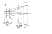
- 2 is a cross-sectional view of an imaging lens of Example 1.
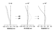
- FIG. FIG. 4 is an aberration diagram of spherical aberration (a), astigmatism (b), and distortion aberration (c) of the imaging lens of Example 1.
- 6 is a cross-sectional view of an imaging lens of Example 2.
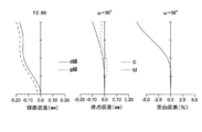
- FIG. FIG. 6 is an aberration diagram of spherical aberration (a), astigmatism (b), and distortion aberration (c) of the imaging lens of Example 2.
- FIG. 6 is a cross-sectional view of an imaging lens of Example 3.
- FIG. FIG. 6 is an aberration diagram of spherical aberration (a), astigmatism (b), and distortion (c) of the imaging lens of Example 3.
- 6 is a cross-sectional view of an imaging lens of Example 4.
- FIG. 6 is an aberration diagram of spherical aberration (a), astigmatism (b), and distortion aberration (c) of the imaging lens of Example 4.
- 6 is a cross-sectional view of an imaging lens of Example 5.
- FIG. FIG. 6 is an aberration diagram of spherical aberration (a), astigmatism (b), and distortion (c) of the imaging lens of Example 5.
- 6 is a cross-sectional view of an imaging lens of Example 6.
- FIG. FIG. FIG. 6 is an aberration diagram of spherical aberration (a), astigmatism (b), and distortion (c) of the imaging lens of Example 5.
- 6 is a cross-sectional view of
- 10 is an aberration diagram of spherical aberration (a), astigmatism (b), and distortion (c) of the imaging lens of Example 6.
- 10 is a cross-sectional view of an imaging lens of Example 7.
- FIG. 10 is an aberration diagram of spherical aberration (a), astigmatism (b), and distortion (c) of the imaging lens of Example 7.
- 10 is a cross-sectional view of an imaging lens of Example 8.
- FIG. 10 is an aberration diagram of spherical aberration (a), astigmatism (b), and distortion aberration (c) of the imaging lens of Example 8.
- 10 is a cross-sectional view of an imaging lens of Example 9.
- FIG. 10 is an aberration diagram of spherical aberration (a), astigmatism (b), and distortion (c) of the imaging lens of Example 9.
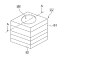
- FIG. 1 is a perspective view of the imaging apparatus
- FIG. 2 is a cross-sectional view of FIG. 1 taken along the line AA.
- the imaging device LU includes an image sensor SR as a solid-state imaging device having a photoelectric conversion unit (light receiving surface) SS, and an imaging lens LN that causes the photoelectric conversion unit SS of the image sensor SR to capture a subject image. And a substrate 52 having an external connection terminal (not shown) that holds the image sensor SR and transmits / receives an electric signal thereof, and these are integrally formed.
- the imaging lens LN includes a first lens block BK1 and a second lens block BK2 in order from the object side (upper side in FIG. 2).
- the first lens block BK1 includes a glass first lens substrate LS1, which is a parallel plate, a resin-made first a lens portion L1a fixed to the object side of the first lens substrate LS1, and an image of the first lens substrate LS1. It consists of 1b lens part L1b made of resin fixed to the surface side.
- the second lens block BK2 includes a glass-made second lens substrate LS2 which is a parallel plate, and a resin-made second a lens portion L2a fixed to the object side of the second lens substrate LS2, and is on the image plane side. Has no lens.
- the first lens substrate LS1, the first a lens unit L1a, and the first b lens unit L1b are different in at least one of the refractive index and the Abbe number, and the second lens substrate LS2 and the second a lens unit L2a or At least one of the refractive index and the Abbe number is different from the second b lens portion L2b.
- the image sensor SR converts an optical image formed on the light receiving surface SS by the imaging lens LN into an electrical signal.
- a CCD (Charge Coupled Device) type image sensor having a plurality of pixels or a CMOS (Complementary Metal-Oxide Semiconductor) type image sensor is used.
- a photoelectric conversion unit SS as a light receiving unit in which pixels (photoelectric conversion elements) are two-dimensionally arranged is formed in the center of a plane on the light receiving side, and a signal processing circuit (not shown) is formed. It is connected to the.
- a signal processing circuit includes a drive circuit unit that sequentially drives each pixel to obtain a signal charge, an A / D conversion unit that converts each signal charge into a digital signal, and a signal that forms an image signal output using the digital signal. It consists of a processing unit and the like.
- a number of pads (not shown) are arranged near the outer edge of the plane on the light receiving side of the image sensor SR and are connected to the substrate 52 via wires (not shown).
- the image sensor SR converts the signal charge from the photoelectric conversion unit SS into an image signal such as a digital YUV signal and outputs the image signal to a predetermined circuit on the substrate 52 via a wire (not shown).
- Y is a luminance signal
- the substrate 52 is connected to an external circuit (for example, a control circuit of a portable terminal mounted with an imaging device) via an external connection terminal (not shown), and a voltage or a clock signal for driving the image sensor SR from the external circuit. It is possible to receive a supply and to output a digital YUV signal to an external circuit.
- an external circuit for example, a control circuit of a portable terminal mounted with an imaging device
- an external connection terminal not shown
- a voltage or a clock signal for driving the image sensor SR from the external circuit. It is possible to receive a supply and to output a digital YUV signal to an external circuit.
- the upper part of the image sensor SR is sealed with a parallel plate PT fixed to the upper surface of the substrate 52.
- the lower end of the spacer member B2 is fixed to the upper surface of the parallel plate PT.
- the second lens block BK2 is fixed to the upper end of the spacer member B2
- the lower end of another spacer member B1 is fixed to the upper surface of the second lens block BK2
- the first end of the spacer member B1 is The lens block BK1 is fixed.
- the imaging device LU provided with the imaging lens LN is a main component of a camera that captures still images and moving images of a subject.
- cameras examples include digital cameras, video cameras, surveillance cameras, in-vehicle cameras, and videophone cameras.
- the camera is incorporated in or removed from a personal computer, a portable terminal (for example, a portable information device terminal such as a cellular phone or a mobile computer), a peripheral device (scanner, printer, etc.) and other digital devices. It may be attached.
- FIG. 3 is a block diagram of a mobile terminal CU which is an example of a digital device with an image input function.
- the imaging device LU mounted on the portable terminal CU includes an imaging lens LN, a parallel plate PT, and an image sensor SR.
- the optical image formed by the imaging lens LN passes through an optical low-pass filter (parallel plate PT in FIG. 3) having a predetermined cutoff frequency characteristic determined by the pixel pitch of the imaging element SR.
- an optical low-pass filter parallel plate PT in FIG. 3
- the spatial frequency characteristics are adjusted so that so-called aliasing noise that occurs when converted into an electrical signal is minimized.
- the parallel plate PT may correspond to an optical filter such as an infrared cut filter or a cover glass of the image sensor SR in addition to the optical low-pass filter.
- an optical filter such as an infrared cut filter or a cover glass of the image sensor SR in addition to the optical low-pass filter.
- the portable terminal CU includes a signal processing unit 1, a control unit 2, a memory 3, an operation unit 4, and a display unit 5 in addition to the imaging device LU.
- the signal processing unit 1 performs predetermined digital image processing and image compression processing on the signal generated by the image sensor SR as necessary.
- the processed signal is recorded as a digital video signal in a memory 3 such as a semiconductor memory or an optical disk, or converted into an infrared signal via a cable and transmitted to another device.
- the control unit 2 is a microcomputer and performs function control such as a photographing function and an image reproduction function intensively.
- the control unit 2 controls the imaging device LU so as to perform at least one of still image shooting and moving image shooting of a subject.
- the memory 3 stores, for example, a signal generated by the image sensor SR and processed by the signal processing unit 1.
- the operation unit 4 is a part including operation members such as an operation button (for example, a release button) and an operation dial (for example, a shooting mode dial), and transmits information input by the operator to the control unit 2.
- operation members such as an operation button (for example, a release button) and an operation dial (for example, a shooting mode dial), and transmits information input by the operator to the control unit 2.
- the display unit 5 includes a display such as a liquid crystal monitor, and performs image display using an image signal converted by the image sensor SR or image information recorded in the memory 3.
- a lens block unit UT in a state where a plurality of lens portions L are fixed to a lens substrate LS made of glass and made of glass and a plurality of lens blocks BK are arranged is a replica method. Manufactured by.
- a curable resin material is transferred onto a lens substrate in a lens shape using a mold. Thereby, a large number of lens portions can be simultaneously manufactured on the lens substrate.
- the first lens block unit UT1 includes a first lens substrate LS1 that is a parallel plate, a plurality of first a lens portions L1a fixed to one plane, and a plurality of first b lens portions L1b fixed to the other plane. It consists of.
- the second lens block unit UT2 is composed of a second lens substrate LS2 that is a parallel plate and a plurality of second a lens portions L2a fixed to one plane thereof.
- the lattice-like spacer member B1 is interposed between the first lens substrate LS1 and the second lens substrate LS2, and keeps the distance between the first lens block unit UT1 and the second lens block unit UT2 constant. Furthermore, the lattice-shaped spacer member B2 is interposed between the parallel plate PT and the second lens substrate LS2, and keeps the distance between the parallel plate PT and the lens block unit UT2 constant.
- the lens portions L1a to L2a are positioned in the lattice hole portions of the spacer members B1 and B2.
- the first lens substrate LS1, the second lens substrate LS2, the spacer members B1 and B2, and the parallel plate PT are cut along the position of the broken line Q of the lattice frame of the spacer members B1 and B2. Then, as shown in FIG. 4C, a plurality of imaging lenses LN are manufactured.
- the spacer members B1 and B2 have a lattice shape, the spacer members B1 and B2 also serve as marks when the imaging lens LN is separated from the member in which the plurality of lens blocks BK1 and BK2 are incorporated. Therefore, the imaging lens LN is easily separated from the member in which the plurality of lens blocks BK1 and BK2 are incorporated, so that no labor is required, and imaging lenses can be mass-produced at low cost.
- the method for manufacturing the imaging lens LN includes the steps of joining the lens substrates through the lattice-shaped spacer member, and the step of cutting the integrated lens substrate and the spacer member with the lattice frame of the spacer member. Have.
- the spacing between the first lens block unit UT1 and the second lens block unit UT2 is kept constant by interposing the spacer member B1 between the first lens substrate LS1 and the second lens substrate LS2.
- the spacer member B1 instead of using the spacer member B1, when the first b lens portion L1b and the second a lens portion L2a are manufactured on the first lens substrate LS1 and the second lens substrate LS2, respectively, the first b lens portion L1b
- the spacer portion may be manufactured integrally with the periphery and the second a lens portion L2a with a curable resin.
- f Focal length of the entire imaging lens fB: Back focus
- F F number 2Y: Diagonal length of imaging surface of solid-state imaging device (diagonal length of rectangular effective pixel region of solid-state imaging device)
- ⁇ Half angle of view
- ENTP Entrance pupil position (distance from first surface to entrance pupil)
- EXTP Exit pupil position (distance from image plane to exit pupil)
- H1 Front principal point position (distance from the first surface to the front principal point)
- H2 Rear principal point position (distance from the final surface to the rear principal point)
- R radius of curvature of refracting surface
- D spacing between top surfaces of axis
- Nd refractive index of lens material d-line at room temperature
- ⁇ d Abbe number of lens material d-line at room temperature *: aspheric surface
- focal length of each lens part In the case of a lens portion formed on the object side of the lens substrate, the value is obtained under the condition that the object side and the
- the shape of the aspherical surface is expressed by the following equation (2), where the vertex of the surface is the origin, the X axis is taken in the optical axis direction, and the height in the direction perpendicular to the optical axis is h.
- Ai i-th order aspheric coefficient
- R radius of curvature
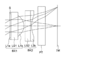
- K conic constant
- a power of 10 for example, 2.5 ⁇ 10 ⁇ 02
- E for example, 2.5E-02
- the surface number of the lens data was given in order with the object side of the first lens as one surface.
- the unit of the numerical value showing the length as described in an Example shall be mm.
- Example 1 ⁇ The overall specifications are shown below.
- the first lens block BK1 includes a first-a lens portion L1a that is convex on the object side, an aperture stop S, a first lens substrate LS1, and a first-b lens portion L1b that is convex on the image side, and has positive refractive power.
- the second lens block BK2 includes a concave second a lens portion L2a and a second lens substrate LS2 on the object side, and has negative refractive power. All surfaces in contact with air in the lens portion are aspherical.
- the parallel plate PT corresponds to an optical low-pass filter, an infrared cut filter, a seal glass of a solid-state image sensor, or the like. Then, the image of the object is formed on the imaging surface IM.
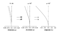
- FIG. 6 is an aberration diagram of spherical aberration (a), astigmatism (b), and distortion aberration (c) of the imaging lens of Example 1.
- d represents the amount of spherical aberration with respect to the d line
- g represents the amount of spherical aberration with respect to the g line.
- the solid line represents the sagittal plane
- the dotted line represents the meridional plane.
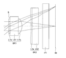
- FIG. 7 is a cross-sectional view of the imaging lens of the second embodiment.
- a first lens block BK1, a second lens block BK2, and a parallel plate PT are provided.
- the first lens block BK1 includes a first-a lens unit L1a that is concave on the object side, an aperture stop S, a first lens substrate LS1, and a first-b lens unit L1b that is convex on the image side, and has positive refractive power.
- the second lens block BK2 includes a second a lens portion L2a and a second lens substrate LS2 that are convex on the object side, and has a positive refractive power. All surfaces in contact with air in the lens portion are aspherical.
- the parallel plate PT corresponds to an optical low-pass filter, an infrared cut filter, a seal glass of a solid-state image sensor, or the like. Then, the image of the object is formed on the imaging surface IM.
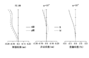
- FIG. 8 is an aberration diagram of spherical aberration (a), astigmatism (b), and distortion (c) of the imaging lens of Example 2.
- d represents the amount of spherical aberration with respect to the d line
- g represents the amount of spherical aberration with respect to the g line.
- the solid line represents the sagittal plane
- the dotted line represents the meridional plane.
- FIG. 9 is a cross-sectional view of the imaging lens of Example 3.
- a first lens block BK1, a second lens block BK2, and a parallel plate PT are provided.
- the first lens block BK1 includes a first-a lens portion L1a that is convex on the object side, an aperture stop S, a first lens substrate LS1, and a first-b lens portion L1b that is convex on the image side, and has positive refractive power.
- the second lens block BK2 includes a second lens substrate LS2 and a second b lens portion L2b that is concave on the image side, and has negative refractive power. All surfaces in contact with air in the lens portion are aspherical.
- the parallel plate PT corresponds to an optical low-pass filter, an infrared cut filter, a seal glass of a solid-state image sensor, or the like. Then, the image of the object is formed on the imaging surface IM.
- FIG. 10 is an aberration diagram of spherical aberration (a), astigmatism (b), and distortion (c) of the imaging lens of Example 3.
- d represents the amount of spherical aberration with respect to the d line
- g represents the amount of spherical aberration with respect to the g line.
- the solid line represents the sagittal plane
- the dotted line represents the meridional plane.
- Example 4 ⁇ The overall specifications are shown below.
- FIG. 11 is a cross-sectional view of the imaging lens of Example 4.
- a first lens block BK1, a second lens block BK2, and a parallel plate PT are provided.
- the first lens block BK1 includes a first-a lens unit L1a that is concave on the object side, an aperture stop S, a first lens substrate LS1, and a first-b lens unit L1b that is convex on the image side, and has positive refractive power.
- the second lens block BK2 includes a second a lens portion L2a that is concave on the object side and a second lens substrate LS2, and has a negative refractive power. All surfaces in contact with air in the lens portion are aspherical.
- the parallel plate PT corresponds to an optical low-pass filter, an infrared cut filter, a seal glass of a solid-state image sensor, or the like. Then, the image of the object is formed on the imaging surface IM.
- FIG. 12 is an aberration diagram of spherical aberration (a), astigmatism (b), and distortion (c) of the imaging lens of Example 4.
- d represents the amount of spherical aberration with respect to the d line
- g represents the amount of spherical aberration with respect to the g line.
- the solid line represents the sagittal plane
- the dotted line represents the meridional plane. (Example 5) ⁇
- the overall specifications are shown below.
- FIG. 13 is a cross-sectional view of the imaging lens of Example 5.
- a first lens block BK1, a second lens block BK2, and a parallel plate PT are provided.
- the first lens block BK1 includes a first-a lens portion L1a that is convex on the object side, an aperture stop S, a first lens substrate LS1, and a first-b lens portion L1b that is convex on the image side, and has positive refractive power.
- the second lens block BK2 includes a second a lens portion L2a and a second lens substrate LS2 that are convex on the object side, and has a positive refractive power. All surfaces in contact with air in the lens portion are aspherical.
- the parallel plate PT corresponds to an optical low-pass filter, an infrared cut filter, a seal glass of a solid-state image sensor, or the like. Then, the image of the object is formed on the imaging surface IM.
- FIG. 14 is an aberration diagram of spherical aberration (a), astigmatism (b), and distortion (c) of the imaging lens of Example 5.
- d represents the amount of spherical aberration with respect to the d line
- g represents the amount of spherical aberration with respect to the g line.
- the solid line represents the sagittal plane
- the dotted line represents the meridional plane.
- FIG. 15 is a sectional view of the imaging lens of Example 6.
- a first lens block BK1, a second lens block BK2, and a parallel plate PT are provided.
- the first lens block BK1 includes a first-a lens portion L1a that is convex on the object side, an aperture stop S, a first lens substrate LS1, and a first-b lens portion L1b that is convex on the image side, and has positive refractive power.
- the second lens block BK2 includes a concave second a lens portion L2a and a second lens substrate LS2 on the object side, and has negative refractive power. All surfaces in contact with air in the lens portion are aspherical.
- the parallel plate PT corresponds to an optical low-pass filter, an infrared cut filter, a seal glass of a solid-state image sensor, or the like. Then, the image of the object is formed on the imaging surface IM.
- FIG. 16 is an aberration diagram of spherical aberration (a), astigmatism (b), and distortion (c) of the imaging lens of Example 6.
- d represents the amount of spherical aberration with respect to the d line
- g represents the amount of spherical aberration with respect to the g line.
- the solid line represents the sagittal plane
- the dotted line represents the meridional plane.
- FIG. 17 is a cross-sectional view of the imaging lens of the seventh embodiment.
- a first lens block BK1, a second lens block BK2, and a parallel plate PT are provided.
- the first lens block BK1 includes a first-a lens unit L1a that is concave on the object side, an aperture stop S, a first lens substrate LS1, and a first-b lens unit L1b that is convex on the image side, and has positive refractive power.
- the second lens block BK2 includes a second lens substrate LS2 and a second b lens portion L2b that is concave on the image side, and has negative refractive power. All surfaces in contact with air in the lens portion are aspherical.
- the parallel plate PT corresponds to an optical low-pass filter, an infrared cut filter, a seal glass of a solid-state image sensor, or the like. Then, the image of the object is formed on the imaging surface IM.
- FIG. 18 is an aberration diagram of spherical aberration (a), astigmatism (b), and distortion (c) of the imaging lens of Example 7.
- d represents the amount of spherical aberration with respect to the d line
- g represents the amount of spherical aberration with respect to the g line.
- the solid line represents the sagittal plane
- the dotted line represents the meridional plane.
- FIG. 19 is a cross-sectional view of the imaging lens of Example 8.
- a first lens block BK1, a second lens block BK2, and a parallel plate PT are provided.
- the first lens block BK1 includes a first-a lens unit L1a that is concave on the object side, an aperture stop S, a first lens substrate LS1, and a first-b lens unit L1b that is convex on the image side, and has positive refractive power.
- the second lens block BK2 includes a concave second a lens portion L2a and a second lens substrate LS2 on the object side, and has negative refractive power. All surfaces in contact with air in the lens portion are aspherical.
- the parallel plate PT corresponds to an optical low-pass filter, an infrared cut filter, a seal glass of a solid-state image sensor, or the like. Then, the image of the object is formed on the imaging surface IM.
- FIG. 20 is an aberration diagram of spherical aberration (a), astigmatism (b), and distortion (c) of the imaging lens of Example 8.
- d represents the amount of spherical aberration with respect to the d line
- g represents the amount of spherical aberration with respect to the g line.
- the solid line represents the sagittal plane
- the dotted line represents the meridional plane.
- Example 9 The overall specifications are shown below.
- FIG. 21 is a cross-sectional view of the imaging lens of Example 9.
- a first lens block BK1, a second lens block BK2, and a parallel plate PT are provided.
- the first lens block BK1 includes a first-a lens portion L1a that is convex on the object side, an aperture stop S, a first lens substrate LS1, and a first-b lens portion L1b that is convex on the image side, and has positive refractive power.
- the second lens block BK2 includes a second lens substrate LS2 and a second b lens portion L2b that is concave on the image side, and has negative refractive power. All surfaces in contact with air in the lens portion are aspherical.
- the parallel plate PT corresponds to an optical low-pass filter, an infrared cut filter, a seal glass of a solid-state image sensor, or the like. Then, the image of the object is formed on the imaging surface IM.
- FIG. 22 is an aberration diagram of spherical aberration (a), astigmatism (b), and distortion (c) of the imaging lens of Example 9.
- d represents the amount of spherical aberration with respect to the d line
- g represents the amount of spherical aberration with respect to the g line.
- the solid line represents the sagittal plane
- the dotted line represents the meridional plane.
- the telecentric characteristics of the image side light beam are not always designed sufficiently.
- shading can be reduced by reviewing the arrangement of the color filters of the solid-state imaging device and the microlens array.
- the angle formed between the principal ray and the optical axis satisfies the following conditional expression.
- a solid-state imaging device in which shading is not noticeable has been developed within the range of the conditional expression. Therefore, this embodiment realizes a wafer-scale lens suitable for mass production while enabling better aberration correction for the reduced requirement for telecentric characteristics and sufficiently supporting the increase in the number of pixels of the solid-state imaging device. Design example.
- ⁇ CRA angle formed between the principal ray of the maximum image light incident on the imaging surface and the optical axis
- Example 1 30 ° Example 2 22 ° Example 3 30 ° Example 4 30 ° Example 5 30 ° Example 6 29 ° Example 7 29 ° Example 8 27 ° Example 9 35 °
- CU mobile terminal LU imaging device SR image sensor LN imaging lens BK1 first lens block BK2 second lens block LS1 first lens substrate LS2 second lens substrate L1a first a lens unit L1b first b lens unit L2a second a lens unit L2b second b Lens part S Aperture stop PT Parallel plate IM Imaging surface
Landscapes
- Physics & Mathematics (AREA)
- General Physics & Mathematics (AREA)
- Optics & Photonics (AREA)
- Lenses (AREA)
Abstract
良好な収差性能で広角化が可能で、低コストでの大量生産が可能な撮像レンズ。 第1レンズ基板の物体側面上に第1aレンズ部が形成されると共に、第1レンズ基板の像側面上に第1bレンズ部が形成され、第1bレンズ部の像側面は像側に凸面形状を有する第1レンズブロックと、第2レンズ基板の物体側面上に第2aレンズ部が形成されるか、または2レンズ基板の像側面上に第2bレンズ部が形成された第2レンズブロックとを備え、開口絞りが第1レンズブロックの第1bレンズ部より物体側に配置され、以下の条件式を満足することを特徴とする。 0.5<f1b/f<1.5 但し、f1b:前記第1bレンズ部の空気中での焦点距離、f:全系の焦点距離
Description
本発明は、CCD(Charge Coupled Devices)型イメージセンサやCMOS(Complementary Metal-Oxide Semiconductor)型イメージセンサ等の固体撮像素子を用いた撮像装置に用いられる撮像レンズに関し、より詳しくは、大量生産に適したウェハスケールのレンズを用いた撮像レンズ、該撮像レンズを備えた撮像装置、及び該撮像装置を備えた携帯端末に関する。
コンパクトで薄型の撮像装置が、携帯電話機やPDA(Personal Digital Assistant)等のコンパクトで薄型の電子機器である携帯端末に搭載されるようになり、これにより遠隔地へ音声情報だけでなく画像情報も相互に伝送することが可能となっている。
これらの撮像装置に使用される撮像素子としては、CCD型イメージセンサやCMOS型イメージセンサ等の固体撮像素子が使用されている。また、近年では、これら撮像素子上に被写体像を形成するためのレンズは、低コスト化のために、大量生産に適した樹脂で形成されるレンズが用いられるようになってきた。特にVGA(Video Graphics Array)クラスの撮像素子に用いられる撮像レンズには、高い量産性と更なる低コスト化が求められている。また、コンパクト化を図るために固体撮像素子も小型化され、それに伴い、素子のサイズも小さくなり、撮像レンズの高性能化が求められている。更に、室内等の狭い場所でも広い範囲が撮影できるように撮像レンズの広角化も求められている。
このような、携帯端末に内蔵される撮像装置に用いる撮像レンズとして、プラスチックレンズ2枚構成の光学系が一般的によく知られている。しかしながら、これらの撮像レンズに対する更なる量産性と高性能化に対する要求が厳しくなってゆく中でその両立は益々困難となっている。
このような問題点を克服するため、平行平板である数インチのガラス基板上にレプリカ法によってレンズ要素を同時に大量に形成し、これらのレンズ要素が多数形成されたガラス基板(レンズウェハ)をセンサウェハと組み合わせた後に切り離し、レンズモジュールを大量生産する手法が提案されている。こうした製法によって製造されたレンズをウェハスケールレンズと呼び、レンズモジュールをウェハスケールレンズモジュールと呼ぶ。
また、レンズモジュールを大量生産する手法と共に、レンズモジュールを低コストで且つ大量に基板に実装する方法として、近年では予め半田がポッティングされた基板に対しIC(Integrated Circuit)チップや、その他の電子部品と共に、レンズモジュールを載置したままリフロー処理(加熱処理)し、半田を溶融させることにより電子部品とレンズモジュールとを基板に同時実装するという手法が提案されており、リフロー処理に耐え得る耐熱性に優れた撮像レンズも求められている。
このような撮像レンズとして、レンズ基板の物体側面及び像側面の両面にレンズ部が形成された1組のレンズブロックを有するものが提案されている(例えば、特許文献1参照)。
また、良好な収差補正の確保を狙い、2組のレンズブロックを有する撮像レンズが特許公報に開示されている(例えば、特許文献2参照)。
しかし、特許文献1に示す撮像レンズにおいては、1組のレンズブロックから成るため、ペッツバール和を小さくすることが難しく、像面湾曲の補正が十分できず、画面周辺部まで良好な性能を確保することができない。
また、特許文献2に示す撮像レンズは、2組のレンズブロックを有する撮像レンズであって、その実施例1~3においては、第1レンズブロック及び第2レンズブロックともレンズ基板の物体側面及び像側面の両面にレンズ部が形成された構成である。このため、収差は十分に補正なされているが、低コスト化においては十分に対応できているとは言い難い。VGAクラスの撮像素子を用いた撮像レンズにおいては、低コスト化と量産性が要求されるので、更なる改良の余地がある。その実施例4~5においては、第1レンズブロックはレンズ基板の物体側面及び像側面の両面にレンズ部が形成され、第2レンズブロックはレンズ基板の物体側面の片側のみにレンズ部が形成された構成の撮像レンズである。このため低コスト化は図られているが、対角の半画角が30°程度と比較的狭い画角であり、更なる広角化を行うと、良好な収差補正を行うことが難しく、製品のラインナップとして、広角化の光学系が求められている状況への十分な対応ができるとは言い難い。
本発明はかかる問題に鑑みてなされたものであり、良好な収差性能を有しながら広角化が可能であり、且つ低コストでの大量生産が可能な撮像レンズ、該撮像レンズを備えた撮像装置、及び該撮像装置を備えた携帯端末を提供することを目的とする。
上記目的は下記に記載した発明により達成される。
本発明の撮像レンズは、物体側から順に、平行平板である第1レンズ基板と、その物体側面及び像側面にそれぞれ形成された二つの第1レンズ部とを備え、前記第1レンズ基板と前記第1レンズ部は屈折率とアッベ数のうち少なくとも一方が異なって、正の屈折力を有する第1レンズブロックと、平行平板である第2レンズ基板と、その物体側面若しくは像側面の何れか一方の面に形成された第2レンズ部とを備え、前記第2レンズ基板と前記第2レンズ部は屈折率とアッベ数のうち少なくとも一方が異なっている第2レンズブロックと、を有する撮像レンズであって、
前記第1レンズ基板の物体側面上に第1aレンズ部が形成されると共に、前記第1レンズ基板の像側面上に第1bレンズ部が形成され、前記第1bレンズ部の像側面は像側に凸面形状を有し、前記第2レンズ基板の物体側面上に第2aレンズ部が形成されるか、または前記第2レンズ基板の像側面上に第2bレンズ部が形成され、開口絞りが前記第1レンズブロックの前記第1bレンズ部より物体側に配置され、以下の条件式を満足することを特徴とする。
前記第1レンズ基板の物体側面上に第1aレンズ部が形成されると共に、前記第1レンズ基板の像側面上に第1bレンズ部が形成され、前記第1bレンズ部の像側面は像側に凸面形状を有し、前記第2レンズ基板の物体側面上に第2aレンズ部が形成されるか、または前記第2レンズ基板の像側面上に第2bレンズ部が形成され、開口絞りが前記第1レンズブロックの前記第1bレンズ部より物体側に配置され、以下の条件式を満足することを特徴とする。
0.5<f1b/f<1.5 (1)
但し、
f1b:前記第1bレンズ部の空気中での焦点距離
f :全系の焦点距離
本発明によれば、良好な収差性能を有しながら、広角化が可能であり、且つ低コストでの大量生産が可能な撮像レンズを提供することができる。
但し、
f1b:前記第1bレンズ部の空気中での焦点距離
f :全系の焦点距離
本発明によれば、良好な収差性能を有しながら、広角化が可能であり、且つ低コストでの大量生産が可能な撮像レンズを提供することができる。
また、レンズ基板を平行平板とすることで、加工が容易になる上に、レンズ部との界面においてパワーを持たず、面精度による像面の焦点位置への影響を低減できる。また、ウェハと略同形状とすることが可能となるため、ウェハスケールレンズの組み立てを容易にできるようになる。
また、レンズブロックを2組構成にすることで、レンズブロックが1組構成のときと比べて諸収差の補正を行い易く、良好な描写性能を確保することができる。また、第2レンズブロックのレンズ部を基板面の片側1枚にすることによって、基板面の両側にレンズ部を形成するレンズブロック2組構成に比べて生産性が良く、低コスト化を図ることができる。
また、第1bレンズ部より物体側に開口絞りを配置し、第1bレンズ部を像側に凸面を向けた正の屈折力とすることで、射出瞳位置を像面から遠ざけることができる。これにより、レンズ最終面を射出した光束の主光線が固体撮像素子に垂直に近い角度で入射するようになり、テレセントリック性を良好に確保することができる。
また、レンズ部とレンズ基板の材質を異ならせることで、屈折率やアッベ数を変えることができるために設計の自由度が増え、収差を良好に補正することができる。
条件式(1)は第1bレンズ部の屈折力を適切に設定する条件である。条件式(1)の下限を上回るようにすることで第1bレンズ部の正のパワーが強くなり過ぎず、ペッツバール和が適切に設定でき、像面湾曲の補正が容易になる。一方、条件式(1)の上限を下回るようにすることで、第1bレンズ部の正のパワーが弱くなり過ぎず、軸外光束のコマフレアや歪曲収差の発生を抑えることができる。
なお、下式の条件式がより望ましい。
0.54<f1b/f<1.30
また、本発明の撮像レンズは、以下の条件式を満足する。
また、本発明の撮像レンズは、以下の条件式を満足する。
0.30<Pair/P<2.0 (2)
但し、
Pairは第1レンズブロックと第2レンズブロック間の空気レンズのパワーで、以下の式で求められる。
但し、
Pairは第1レンズブロックと第2レンズブロック間の空気レンズのパワーで、以下の式で求められる。
Pair=(1-N1i)/R1i+(N2o-1)/R2o-D・{(1-N1i)・(N2o-1)/(R1i・R2o)}
但し、
R1i:第1レンズブロックの最も像側の面の曲率半径
R2o:は第2レンズブロックの最も物体側の面の曲率半径
N1i:第1レンズブロックの最も像側の面のd線の屈折率
N2o:第2レンズブロックの最も物体側の面のd線の屈折率
D :第1レンズブロックと第2レンズブロックとの光軸上の距離
条件式(2)は第1レンズブロックと第2レンズブロックの間の空気レンズのパワーを適切に設定するものである。条件式(2)の下限を上回るようにすることで、第1レンズブロックと第2レンズブロックの間の空気レンズのパワーが弱くなり過ぎず、画面周辺に結像する光線を跳ね上げ、最終レンズブロックでのテレセントリック性を良好に確保することができる。一方、条件式(2)の上限を下回るようにすることで、第1レンズブロックと第2レンズブロックの間の空気レンズのパワーが強くなり過ぎず、ペッツバール和が適切に設定でき、像面湾曲の補正が容易になる。
但し、
R1i:第1レンズブロックの最も像側の面の曲率半径
R2o:は第2レンズブロックの最も物体側の面の曲率半径
N1i:第1レンズブロックの最も像側の面のd線の屈折率
N2o:第2レンズブロックの最も物体側の面のd線の屈折率
D :第1レンズブロックと第2レンズブロックとの光軸上の距離
条件式(2)は第1レンズブロックと第2レンズブロックの間の空気レンズのパワーを適切に設定するものである。条件式(2)の下限を上回るようにすることで、第1レンズブロックと第2レンズブロックの間の空気レンズのパワーが弱くなり過ぎず、画面周辺に結像する光線を跳ね上げ、最終レンズブロックでのテレセントリック性を良好に確保することができる。一方、条件式(2)の上限を下回るようにすることで、第1レンズブロックと第2レンズブロックの間の空気レンズのパワーが強くなり過ぎず、ペッツバール和が適切に設定でき、像面湾曲の補正が容易になる。
なお、下式の条件式がより望ましい。
0.60<Pair/P<1.82
また、本発明の撮像レンズは、前記第2レンズ基板の物体側面上に前記第2aレンズ部が形成され、前記第2aレンズ部の物体側面は光軸近傍において物体側に凸面形状を有し、以下の条件式を満足することを特徴とする。
また、本発明の撮像レンズは、前記第2レンズ基板の物体側面上に前記第2aレンズ部が形成され、前記第2aレンズ部の物体側面は光軸近傍において物体側に凸面形状を有し、以下の条件式を満足することを特徴とする。
0.0<f1/f2<0.8 (3)
但し、
f1:前記第1レンズブロックの合成焦点距離
f2:前記第2レンズブロックの合成焦点距離
本請求項の如く構成すると、第2レンズブロックは正の屈折力を有し、正の屈折力を有する第1レンズブロックと第2レンズブロックは対称に近い構成をとるため、歪曲収差の補正が容易になる。また、第2aレンズ部の物体側面は光軸近傍において物体側に凸面形状にすることにより、最終レンズによる画面周辺に結像する光線の跳ね上げを抑え、テレセントリック性を容易に確保することができる。
但し、
f1:前記第1レンズブロックの合成焦点距離
f2:前記第2レンズブロックの合成焦点距離
本請求項の如く構成すると、第2レンズブロックは正の屈折力を有し、正の屈折力を有する第1レンズブロックと第2レンズブロックは対称に近い構成をとるため、歪曲収差の補正が容易になる。また、第2aレンズ部の物体側面は光軸近傍において物体側に凸面形状にすることにより、最終レンズによる画面周辺に結像する光線の跳ね上げを抑え、テレセントリック性を容易に確保することができる。
条件式(3)の下限を上回るようにすることで、第1レンズブロックに比べ第2レンズブロックの屈折力が弱くなり過ぎず、テレセントリック性が良好に確保することができる。一方、条件式(3)の上限を下回るようにすることで、第1レンズブロックに比べ第2レンズブロックの屈折力が強くなり過ぎず、ペッツバール和が適切に設定でき、像面湾曲の補正が容易になる。
なお、下式の条件式がより望ましい。
0.05<f1/f2<0.58
また、本発明の撮像レンズは、前記第2レンズ基板の物体側面上に前記第2aレンズ部が形成され、前記第2aレンズ部の物体側面は光軸近傍において物体側に凹面形状を有し、以下の条件式を満足することを特徴とする。
また、本発明の撮像レンズは、前記第2レンズ基板の物体側面上に前記第2aレンズ部が形成され、前記第2aレンズ部の物体側面は光軸近傍において物体側に凹面形状を有し、以下の条件式を満足することを特徴とする。
0.0<f1/|f2|<0.8 (4)
但し、
f1:第1レンズブロックの合成焦点距離
f2:第2レンズブロックの合成焦点距離
本請求項の如く構成すると、第2レンズブロックの負の屈折力により、ペッツバール和が小さくできるので、像面湾曲を良好に補正することができる。
但し、
f1:第1レンズブロックの合成焦点距離
f2:第2レンズブロックの合成焦点距離
本請求項の如く構成すると、第2レンズブロックの負の屈折力により、ペッツバール和が小さくできるので、像面湾曲を良好に補正することができる。
条件式(4)の下限を上回るようにすることで、第1レンズブロックに比べ第2レンズブロックの負の屈折力が弱くなり過ぎず、ペッツバール和が適切に設定でき、像面湾曲の補正が容易になる。一方、条件式(4)の上限を下回るようにすることで、第1レンズブロックに比べ第2レンズブロックの負の屈折力が強くなり過ぎず、テレセントリック性を良好に確保することができる。
なお、下式の条件式がより望ましい。
0.0<f1/|f2|<0.6
また、本発明の撮像レンズは、前記第2レンズ基板の像側面上に前記第2bレンズ部が形成され、前記第2bレンズ部の像側面は光軸近傍において像側に凹面形状を有し、以下の条件式を満足することを特徴とする。
また、本発明の撮像レンズは、前記第2レンズ基板の像側面上に前記第2bレンズ部が形成され、前記第2bレンズ部の像側面は光軸近傍において像側に凹面形状を有し、以下の条件式を満足することを特徴とする。
0.4<f1/|f2|<0.8 (5)
但し、
f1:第1レンズブロックの合成焦点距離
f2:第2レンズブロックの合成焦点距離
本請求項の如く構成すると、第2レンズブロックの負の屈折力により、ペッツバール和が小さくできるので、像面湾曲を良好に補正することができる。
但し、
f1:第1レンズブロックの合成焦点距離
f2:第2レンズブロックの合成焦点距離
本請求項の如く構成すると、第2レンズブロックの負の屈折力により、ペッツバール和が小さくできるので、像面湾曲を良好に補正することができる。
条件式(5)の下限を上回るようにすることで、第1レンズブロックに比べ第2レンズブロックの負の屈折力が弱くなり過ぎず、ペッツバール和が適切に設定でき、像面湾曲の補正が容易になる。一方、条件式(5)の上限を下回るようにすることで、第1レンズブロックに比べ第2レンズブロックの負の屈折力が強くなり過ぎず、テレセントリック性を良好に確保することができる。
なお、下式の条件式がより望ましい。
0.43<f1/|f2|<0.70
さらに、下式の条件式がより望ましい。
さらに、下式の条件式がより望ましい。
0.50<f1/|f2|<0.70
また、本発明の撮像レンズは、以下の条件式を満足することを特徴とする。
また、本発明の撮像レンズは、以下の条件式を満足することを特徴とする。
0.5<(R1a+R1b)/(R1a-R1b)<1.5 (6)
但し、
R1a:第1aレンズ部の曲率半径
R1b:第1bレンズ部の曲率半径
条件式(6)は、第1レンズブロックのシェーピングファクターを適切に設定するものである。条件式(6)の下限を上回るようにすることで、第1レンズブロックの正の屈折力を主に第1bレンズ部で担うことになり、撮像レンズ全系でのテレセントリック性確保が容易になる。また、かかる値が上限を下回るようにすることで、第1bレンズ部の曲率半径が極端に小さくなることがなくなり、撮像レンズ全系のバックフォーカスを確保でき、広角化にも有利である。
但し、
R1a:第1aレンズ部の曲率半径
R1b:第1bレンズ部の曲率半径
条件式(6)は、第1レンズブロックのシェーピングファクターを適切に設定するものである。条件式(6)の下限を上回るようにすることで、第1レンズブロックの正の屈折力を主に第1bレンズ部で担うことになり、撮像レンズ全系でのテレセントリック性確保が容易になる。また、かかる値が上限を下回るようにすることで、第1bレンズ部の曲率半径が極端に小さくなることがなくなり、撮像レンズ全系のバックフォーカスを確保でき、広角化にも有利である。
なお、下式の条件式がより望ましい。
0.56<(R1a+R1b)/(R1a-R1b)<1.47
さらに、下式の条件式がより望ましい。
さらに、下式の条件式がより望ましい。
0.56<(R1a+R1b)/(R1a-R1b)<1.20
また、本発明の撮像レンズは、前記第2レンズ基板のうち、物体側基板面若しくは像側基板面の何れか一方の前記第2レンズ部を備えない基板面上にIRカットコートを施したことを特徴とする。
また、本発明の撮像レンズは、前記第2レンズ基板のうち、物体側基板面若しくは像側基板面の何れか一方の前記第2レンズ部を備えない基板面上にIRカットコートを施したことを特徴とする。
第2レンズブロックの物体側若しくは像側基板面のうち、レンズ部のない基板面へIR(Infra Red)カットコートやAR(Anti-Reflection)コートを施すことで、光学部材の削減が可能であり、低コスト化と量産性を向上させることができる。
また、本発明の撮像レンズは、前記第1レンズ基板及び前記第2レンズ基板はガラス材料より形成されていることを特徴とする。
レンズ基板をガラスより形成することで、ガラスは樹脂に比べて軟化温度が高いのでリフロー処理を行っても容易に変異せず、また低コスト化できる。更に、高軟化温度のガラスを用いることがより望ましい。
また、本発明の撮像レンズは、前記第1レンズ部及び第2レンズ部は樹脂材料より形成されていることを特徴とする。
レンズ部を樹脂材料より形成することで、ガラスを用いる場合に比べて加工成形性が良くなり、また低コスト化できる。
また、本発明の撮像レンズは、前記樹脂材料は硬化型樹脂材料であることを特徴とする。
レンズ部を硬化型の樹脂材料によって形成することで、ウェハ状のレンズ基板に金型によって同時に大量にレンズ部を種々の手段によって硬化させることが可能となり、量産性を向上させることができる。
ここで、硬化型の樹脂材料とは、熱によって硬化する樹脂材料や光によって硬化する樹脂材料等を指す。なお、硬化型の樹脂材料はUV硬化型の樹脂材料であることが望ましい。UV硬化型の樹脂材料にすることにより、硬化時間を短くでき、量産性を改善できる。また、近年では耐熱性に優れた樹脂及び硬化型の樹脂材料が開発されており、リフロー処理にも耐えることができる。
また、本発明の撮像レンズは、前記樹脂材料は30ナノメートル以下の無機微粒子が分散されていることを特徴とする。
樹脂材料にて構成されるレンズ部に30ナノメートル以下の無機微粒子を分散させることで、温度が変化しても性能の劣化や、像点位置変動を低減でき、しかも光透過率を低下させることなく、環境変化に関わらず優れた光学特性を有する撮像レンズを提供できる。
一般に透明な樹脂材料に微粒子を混合させると、光の散乱が生じ透過率が低下するため、光学材料として使用することは困難であったが、微粒子の大きさを透過光束の波長より小さくすることにより、散乱が実質的に発生しないようにできる。
また、樹脂材料はガラス材料に比べて屈折率が低いことが欠点であったが、屈折率の高い無機粒子を母材となる樹脂材料に分散させると、屈折率を高くできることが分かってきた。具体的には、母材となる樹脂材料に30ナノメートル以下、望ましくは20ナノメートル以下、更に望ましくは15ナノメートル以下の無機粒子を分散させることにより、任意の屈折率を有する材料を提供できる。
更に、樹脂材料は温度が上昇することにより屈折率が低下してしまうが、温度が上昇すると屈折率が上昇する無機粒子を母材となる樹脂材料に分散させると、これらの性質を打ち消しあうように作用するので、温度変化に対する屈折率変化を小さくできることも知られている。逆に、温度が上昇すると屈折率が低下する無機粒子を母材となる樹脂材料に分散させると、温度変化に対する屈折率変化を大きくできることも知られている。具体的には、母材となるプラスチック材料に30ナノメートル以下、なお、望ましくは、母材となる樹脂材料に20ナノメートル以下、望ましくは15ナノメートル以下の無機粒子を分散させることにより、任意の温度依存性を有する材料を提供できる。
例えば、アクリル系樹脂に酸化アルミニウム(Al2O3)やニオブ酸リチウム(LiNbO3)の微粒子を分散させることにより、高い屈折率のプラスチック材料が得られると共に、温度に対する屈折率変化を小さくすることができる。
次に、屈折率の温度変化Aについて詳細に説明する。屈折率の温度変化Aは、ローレンツ・ローレンツの式に基づいて、屈折率nを温度tで微分することにより、以下の数1の式で表される。

但し、
α:線膨張係数
[R]:分子屈折
樹脂材料の場合は、一般に上記数式中第1項に比べ第2項の寄与が小さく、ほぼ無視できる。例えば、PMMA樹脂の場合、線膨張係数αは7×10⁻⁵であり、上記式に代入すると、dn/dt=-1.2×10-4[/℃]となり、実測値と概ね一致する。
α:線膨張係数
[R]:分子屈折
樹脂材料の場合は、一般に上記数式中第1項に比べ第2項の寄与が小さく、ほぼ無視できる。例えば、PMMA樹脂の場合、線膨張係数αは7×10⁻⁵であり、上記式に代入すると、dn/dt=-1.2×10-4[/℃]となり、実測値と概ね一致する。
ここで、微粒子、望ましくは無機微粒子を樹脂材料中に分散させることにより、実質的に上記数式の第2項の寄与を大きくし、第1項の線膨張による変化と打ち消しあうようにさせている。具体的には、従来は-1.2×10⁻⁴程度であった変化を、絶対値で8×10⁻⁵未満に抑えることが望ましい。
また、第2項の寄与を更に大きくして、母材の樹脂材料とは逆の温度特性を持たせることも可能である。つまり、温度が上昇することによって屈折率が低下するのではなく、逆に、屈折率が上昇するような素材を得ることもできる。
混合させる割合は、屈折率の温度に対する変化の割合をコントロールするために、適宜増減できるし、複数種類のナノサイズの無機粒子をブレンドして分散させることも可能である。
また、本発明の撮像レンズは、被写体像を結像させる撮像レンズ部、またはこれを含む固体撮像素子を複数製造する製造方法において、格子状のスペーサ部材を介してレンズ基板同士をシールする工程と、一体化された前記レンズ基板及び前記スペーサ部材を前記スペーサ部材の格子枠で切断する工程と、を有する製造方法により製造されたことを特徴とする。
本発明により、安価な撮像レンズを量産することができる。
また、本発明の撮像装置は、上記の撮像レンズを備えたことを特徴とする。
本発明により、低コストで高性能を有した撮像装置を提供することができる。
また、本発明の携帯端末は、上記の撮像装置を備えたことを特徴とする。
本発明により、低コストで高性能を有した携帯端末を提供することができる。
本発明の撮像レンズ、撮像装置及び携帯端末によれば、良好な収差性能を有しながら、広角化が可能であり、かつ低コストでの大量生産が可能になるという効果を奏する。
以下に本発明の実施の形態を図面に基づいて説明する。図1は撮像装置の斜視図、図2は図1を矢印A-A線で切断した断面図である。
図2に示すように、撮像装置LUは、光電変換部(受光面)SSを有する固体撮像素子としてのイメージセンサSRと、イメージセンサSRの光電変換部SSに被写体像を撮像させる撮像レンズLNと、イメージセンサSRを保持すると共にその電気信号の送受を行う不図示の外部接続用端子を有する基板52とを備え、これらが一体的に形成されている。なお、撮像レンズLNは、物体側(図2の上方)から順に、第1レンズブロックBK1と、第2レンズブロックBK2とから構成される。
第1レンズブロックBK1は、平行平板であるガラス製の第1レンズ基板LS1と、第1レンズ基板LS1の物体側に固着された樹脂製の第1aレンズ部L1aと、第1レンズ基板LS1の像面側に固着された樹脂製の第1bレンズ部L1bとからなる。一方、第2レンズブロックBK2は、平行平板であるガラス製の第2レンズ基板LS2と、第2レンズ基板LS2の物体側に固着された樹脂製の第2aレンズ部L2aとからなり、像面側にはレンズ部がない。但し、第2レンズ基板LS2の物体側にレンズ部がなく、二点鎖線で示す如く第2レンズ基板LS2の像面側に樹脂製の第2bレンズ部L2bが固着されている第2レンズブロックBK2でもよい。
そして、第1レンズ基板LS1と、第1aレンズ部L1a及び第1bレンズ部L1bとは、屈折率及びアッベ数のうち少なくとも一方が異なっており、第2レンズ基板LS2と、第2aレンズ部L2a若しくは第2bレンズ部L2bとは、屈折率及びアッベ数のうち少なくとも一方が異なっている。
イメージセンサSRは、撮像レンズLNにより受光面SS上に形成された光学像を電気的な信号に変換する。例えば、複数の画素を有するCCD(Charge Coupled Device)型イメージセンサやCMOS(Complementary Metal-Oxide Semiconductor)型イメージセンサが用いられる。
イメージセンサSRは、その受光側の平面の中央部に、画素(光電変換素子)が2次元的に配置された、受光部としての光電変換部SSが形成されており、不図示の信号処理回路に接続されている。かかる信号処理回路は、各画素を順次駆動し信号電荷を得る駆動回路部と、各信号電荷をデジタル信号に変換するA/D変換部と、このデジタル信号を用いて画像信号出力を形成する信号処理部等から構成されている。また、イメージセンサSRの受光側の平面の外縁近傍には、不図示の多数のパッドが配置されており、不図示のワイヤを介して基板52に接続されている。イメージセンサSRは、光電変換部SSからの信号電荷をデジタルYUV信号等の画像信号等に変換し、不図示のワイヤを介して基板52上の所定の回路に出力する。ここで、Yは輝度信号、U(=R-Y)は赤と輝度信号との色差信号、V(=B-Y)は青と輝度信号との色差信号である。
基板52は、不図示の外部接続用端子を介して外部回路(例えば、撮像装置を実装した携帯端末の制御回路)と接続し、外部回路からイメージセンサSRを駆動するための電圧やクロック信号の供給を受けたり、また、デジタルYUV信号を外部回路へ出力したりすることを可能とする。
イメージセンサSRの上部は、基板52の上面に固定された平行平板PTにより封止されている。平行平板PTの上面には、スペーサ部材B2の下端が固定されている。更に、スペーサ部材B2の上端には、第2レンズブロックBK2が固定され、第2レンズブロックBK2の上面には、別のスペーサ部材B1の下端が固定され、スペーサ部材B1の上端には、第1レンズブロックBK1が固定されている。
撮像レンズLNを備えた撮像装置LUは被写体の静止画及び動画を撮影するカメラの主たる構成要素である。
カメラの例としては、デジタルカメラ、ビデオカメラ、監視カメラ、車載カメラ及びテレビ電話用カメラが挙げられる。また、カメラは、パーソナルコンピュータ、携帯端末(例えば、携帯電話、モバイルコンピュータ等のコンパクトで携帯可能な情報機器端末)、これらの周辺機器(スキャナー、プリンター等)及びその他のデジタル機器等に内蔵または外付けされてもよい。
図3は、画像入力機能付きデジタル機器の一例である携帯端末CUのブロック図である。携帯端末CUに搭載されている撮像装置LUは、撮像レンズLN、平行平板PT及びイメージセンサSRを含む。
撮像レンズLNで形成される光学像は、撮像素子SRの画素ピッチにより決定される所定の遮断周波数特性を有する光学的ローパスフィルター(図3の平行平板PT)を通過する。この通過により、電気的な信号に変換される場合に発生するいわゆる折り返しノイズが最小化されるように、空間周波数特性が調整される。
そして、この空間周波数特性の調整により、色モアレの発生が抑えられる。但し、解像限界周波数周辺の性能が抑えられれば、光学的ローパスフィルタを用いなくても、ノイズが発生しない。また、ノイズのあまり目立たない表示系(例えば、携帯電話の液晶画面等)を用いて、ユーザーが撮影や鑑賞を行う場合、光学的ローパスフィルタは不要である。
平行平板PTは、光学的ローパスフィルタ以外に、赤外カットフィルタ等の光学フィルタや、イメージセンサSRのカバーガラスに相当することもある。
ところで、携帯端末CUは、撮像装置LUの他に、信号処理部1、制御部2、メモリ3、操作部4、及び表示部5を有する。
信号処理部1は、イメージセンサSRで生成された信号に対して所定のデジタル画像処理及び画像圧縮処理を必要に応じて施す。そして、処理が施された信号は、デジタル映像信号として半導体メモリや光ディスク等のメモリ3に記録されたり、ケーブルを介して赤外線信号に変換され、他の機器に伝送されたりする。
制御部2は、マイクロコンピュータであり、撮影機能、画像再生機能等の機能制御等を集中的に行う。例えば、制御部2は、被写体の静止画撮影及び動画撮影のうちの少なくとも一方を行うように、撮像装置LUを制御する。
メモリ3は、例えば、撮像素子SRで生成されるとともに信号処理部1にて処理された信号を記憶する。
操作部4は、操作ボタン(例えばレリーズボタン)、操作ダイヤル(例えば撮影モードダイヤル)等の操作部材を含む部分であり、操作者の操作入力した情報を制御部2に伝達する。
表示部5は、液晶モニター等のディスプレイを含む部分であり、イメージセンサSRによって変換された画像信号またはメモリ3に記録されている画像情報を用いて画像表示を行う。
次に、撮像レンズLNの製造方法について図4を参照して説明する。
先ず、図4(a)の断面図において、平行平板であってガラスから成るレンズ基板LSに複数のレンズ部Lが固着され、複数のレンズブロックBKを並べた状態のレンズブロックユニットUTをレプリカ法で製造する。
レプリカ法は、レンズ基板上に、金型を用いて硬化性の樹脂材料をレンズ形状にして転写する。これにより、レンズ基板上に多数のレンズ部を同時に製造することができる。
このようにして製造されたレンズブロックユニットUTから撮像レンズLNを製造する工程を、図4(b)の概略断面図で示す。
第1レンズブロックユニットUT1は、平行平板である第1レンズ基板LS1と、その一方の平面に固着された複数の第1aレンズ部L1aと、他方の平面に固着された複数の第1bレンズ部L1bとで構成される。
第2レンズブロックユニットUT2は、平行平板である第2レンズ基板LS2と、その一方の平面に固着された複数の第2aレンズ部L2aとで構成される。
格子状のスペーサ部材B1は、第1レンズ基板LS1と第2レンズ基板LS2との間に介在し、第1レンズブロックユニットUT1と第2レンズブロックユニットUT2の間隔を一定に保つ。更に、格子状のスペーサ部材B2は、平行平板PTと第2レンズ基板LS2との間に介在し、平行平板PTとレンズブロックユニットUT2との間隔を一定に保つ。そして、スペーサ部材B1,B2の格子の穴の部分に、各レンズ部L1a~L2aが位置する。
このようにして一体化した状態で、第1レンズ基板LS1、第2レンズ基板LS2、スペーサ部材B1,B2及び平行平板PTが、スペーサ部材B1,B2の格子枠の破線Qの位置に沿って切断され、図4(c)に示すように複数の撮像レンズLNが製造される。
この結果、撮像レンズLN毎のレンズ間隔の調整及び組み立てが不要になり、撮像レンズLNの大量生産が可能となる。
しかも、スペーサ部材B1,B2が格子形状であるので、スペーサ部材B1,B2が、複数のレンズブロックBK1,BK2が組み込まれた部材から撮像レンズLNを切り離す場合の印にもなる。従って、複数のレンズブロックBK1,BK2の組み込まれた部材から撮像レンズLNが簡単に切り離されて手間が掛からず、撮像レンズを安価に大量生産できる。
以上の如く撮像レンズLNの製造方法は、格子状のスペーサ部材を介してレンズ基板同士を接合する工程と、一体化されたレンズ基板及びスペーサ部材をスペーサ部材の格子枠で切断する工程と、を有する。
なお、以上の説明においては、第1レンズ基板LS1と第2レンズ基板LS2との間にスペーサ部材B1を介在させることにより第1レンズブロックユニットUT1と第2レンズブロックユニットUT2の間隔を一定に保つように構成したが、スペーサ部材B1を用いる代わりに、第1bレンズ部L1b及び第2aレンズ部L2aをそれぞれ第1レンズ基板LS1及び第2レンズ基板LS2に製造する際に、第1bレンズ部L1bの周囲及び第2aレンズ部L2aにスペーサ部を硬化性樹脂により一体的に製造するようにしてもよい。
次に、上述した実施の形態に好適な撮像レンズの実施例について説明する。但し、以下に示す実施例により本発明が限定されるものではない。実施例における各符号の意味は以下の通りである。
f :撮像レンズ全系の焦点距離
fB:バックフォーカス
F :Fナンバー
2Y:固体撮像素子の撮像面対角線長(固体撮像素子の矩形実効画素領域の対角線長)
ω :半画角
ENTP:入射瞳位置(第1面から入射瞳までの距離)
EXTP:射出瞳位置(像面から射出瞳までの距離)
H1:前側主点位置(第1面から前側主点までの距離)
H2:後側主点位置(最終面から後側主点までの距離)
R :屈折面の曲率半径
D :軸上面間隔
Nd:レンズ材料のd線の常温での屈折率
νd:レンズ材料のd線の常温でのアッベ数
* :非球面
但し、各レンズ部の焦点距離は、レンズ基板の物体側に形成されるレンズ部の場合は、そのレンズの物体側及び像側が空気で満たされるという状態のもとで求められた値である。また、レンズ基板の像側に形成されるレンズ部の場合も、そのレンズの物体側及び像側が空気で満たされるという状態のもとで求められた値である。
fB:バックフォーカス
F :Fナンバー
2Y:固体撮像素子の撮像面対角線長(固体撮像素子の矩形実効画素領域の対角線長)
ω :半画角
ENTP:入射瞳位置(第1面から入射瞳までの距離)
EXTP:射出瞳位置(像面から射出瞳までの距離)
H1:前側主点位置(第1面から前側主点までの距離)
H2:後側主点位置(最終面から後側主点までの距離)
R :屈折面の曲率半径
D :軸上面間隔
Nd:レンズ材料のd線の常温での屈折率
νd:レンズ材料のd線の常温でのアッベ数
* :非球面
但し、各レンズ部の焦点距離は、レンズ基板の物体側に形成されるレンズ部の場合は、そのレンズの物体側及び像側が空気で満たされるという状態のもとで求められた値である。また、レンズ基板の像側に形成されるレンズ部の場合も、そのレンズの物体側及び像側が空気で満たされるという状態のもとで求められた値である。
各実施例において非球面の形状は、面の頂点を原点とし、光軸方向にX軸をとり、光軸と垂直方向の高さをhとして、以下の数2の式で表される。

但し、
Ai:i次の非球面係数
R :曲率半径
K :円錐定数
また、以降において、10のべき乗数(例えば、2.5×10-02)を、E(例えば2.5E-02)を用いて表すものとする。また、レンズデータの面番号は第1レンズの物体側を1面として順に付与した。なお、実施例に記載の長さを表す数値の単位は全てmmとする。
(実施例1)
・全体諸元を以下に示す。
Ai:i次の非球面係数
R :曲率半径
K :円錐定数
また、以降において、10のべき乗数(例えば、2.5×10-02)を、E(例えば2.5E-02)を用いて表すものとする。また、レンズデータの面番号は第1レンズの物体側を1面として順に付与した。なお、実施例に記載の長さを表す数値の単位は全てmmとする。
(実施例1)
・全体諸元を以下に示す。
f=1.38mm
fB=0.25mm
F=2.88
2Y=1.8mm
ω=37°
ENTP=0.11mm
EXTP=-1.41mm
H1=0.41mm
H2=-1.04mm
・面データを以下に示す。
fB=0.25mm
F=2.88
2Y=1.8mm
ω=37°
ENTP=0.11mm
EXTP=-1.41mm
H1=0.41mm
H2=-1.04mm
・面データを以下に示す。
面番号 R(mm) D(mm) Nd νd 有効半径(mm)
1(*) 1.920 0.17 1.572 35 0.31
2(絞り) ∞ 0.49 1.520 62 0.23
3 ∞ 0.35 1.514 57 0.42
4(*) -0.421 0.06 0.47
5(*) -0.753 0.05 1.572 35 0.50
6 ∞ 0.30 1.520 62 0.54
7 ∞ 0.20 0.62
8 ∞ 0.35 1.516 64 0.70
9 ∞ 0.35 0.79
・非球面係数を以下に示す。
第1面
K=0.00000E+00,A4=0.61999E+00,A6=-0.22885E+02,A8=0.25788E+03,A10=-0.10428E+04,A12=0.00000E+00
第2面
K=-0.14092E+01,A4=0.10405E+01,A6=0.22778E+01,A8=-0.45239E+02,A10=0.13002E+03,A12=-0.93639E+02
第3面
K=0.00000E+00,A4=0.27083E+01,A6=-0.77844E+01,A8=0.13377E+02,A10=-0.23199E+02,A12=0.39765E+02
・レンズブロックデータを以下に示す。
1(*) 1.920 0.17 1.572 35 0.31
2(絞り) ∞ 0.49 1.520 62 0.23
3 ∞ 0.35 1.514 57 0.42
4(*) -0.421 0.06 0.47
5(*) -0.753 0.05 1.572 35 0.50
6 ∞ 0.30 1.520 62 0.54
7 ∞ 0.20 0.62
8 ∞ 0.35 1.516 64 0.70
9 ∞ 0.35 0.79
・非球面係数を以下に示す。
第1面
K=0.00000E+00,A4=0.61999E+00,A6=-0.22885E+02,A8=0.25788E+03,A10=-0.10428E+04,A12=0.00000E+00
第2面
K=-0.14092E+01,A4=0.10405E+01,A6=0.22778E+01,A8=-0.45239E+02,A10=0.13002E+03,A12=-0.93639E+02
第3面
K=0.00000E+00,A4=0.27083E+01,A6=-0.77844E+01,A8=0.13377E+02,A10=-0.23199E+02,A12=0.39765E+02
・レンズブロックデータを以下に示す。
レンズブロック 始面 終面 焦点距離(mm)
1 1 4 0.78
2 5 7 -1.32
・各条件式に対応する値を以下に示す。
(1)f1b/f=0.595
(2)Pair/P=0.704
(4)f1/|f2|=0.594
(6)(R1a+R1b)/(R1a-R1b)=0.641
図5は実施例1の撮像レンズの断面図である。物体側から順に、第1レンズブロックBK1、第2レンズブロックBK2及び平行平板PTが設けられている。第1レンズブロックBK1は物体側に凸の第1aレンズ部L1a、開口絞りS、第1レンズ基板LS1及び像側に凸の第1bレンズ部L1bより構成され、正の屈折力を有している。第2レンズブロックBK2は物体側に凹の第2aレンズ部L2a及び第2レンズ基板LS2より構成され、負の屈折力を有している。また、レンズ部における空気と接する全ての面は非球面形状である。平行平板PTは光学的ローパスフィルタ、赤外カットフィルタ若しくは固体撮像素子のシールガラス等に相当する。そして、物体の像は撮像面IMに結像する。
1 1 4 0.78
2 5 7 -1.32
・各条件式に対応する値を以下に示す。
(1)f1b/f=0.595
(2)Pair/P=0.704
(4)f1/|f2|=0.594
(6)(R1a+R1b)/(R1a-R1b)=0.641
図5は実施例1の撮像レンズの断面図である。物体側から順に、第1レンズブロックBK1、第2レンズブロックBK2及び平行平板PTが設けられている。第1レンズブロックBK1は物体側に凸の第1aレンズ部L1a、開口絞りS、第1レンズ基板LS1及び像側に凸の第1bレンズ部L1bより構成され、正の屈折力を有している。第2レンズブロックBK2は物体側に凹の第2aレンズ部L2a及び第2レンズ基板LS2より構成され、負の屈折力を有している。また、レンズ部における空気と接する全ての面は非球面形状である。平行平板PTは光学的ローパスフィルタ、赤外カットフィルタ若しくは固体撮像素子のシールガラス等に相当する。そして、物体の像は撮像面IMに結像する。
図6は、実施例1の撮像レンズの球面収差(a)、非点収差(b)及び歪曲収差(c)の収差図である。ここで、球面収差図において、dはd線、gはg線に対する球面収差量をそれぞれ表す。また、非点収差図において、実線はサジタル面、点線はメリディオナル面をそれぞれ表す。
(実施例2)
・全体諸元を以下に示す。
(実施例2)
・全体諸元を以下に示す。
f=1.32mm
fB=0.05mm
F=2.88
2Y=1.8mm
ω=36°
ENTP=0.03mm
EXTP=-2.40mm
H1=0.66mm
H2=-1.19mm
・面データを以下に示す。
fB=0.05mm
F=2.88
2Y=1.8mm
ω=36°
ENTP=0.03mm
EXTP=-2.40mm
H1=0.66mm
H2=-1.19mm
・面データを以下に示す。
面番号 R(mm) D(mm) Nd νd 有効半径(mm)
1* -13.100 0.05 1.572 35 0.25
2(絞り) ∞ 0.30 1.520 62 0.23
3 ∞ 0.21 1.514 57 0.36
4(*) -0.877 0.68 0.41
5(*) 1.802 0.13 1.572 35 0.70
6 ∞ 0.30 1.520 62 0.71
7 ∞ 0.20 0.77
8 ∞ 0.35 1.516 64 0.82
9 ∞ 0.14 0.88
・非球面係数を以下に示す。
第1面
K=0.00000E+00,A4=0.30628E+01,A6=-0.11599E+03,A8=0.17438E+04,A10=-0.97206E+04,A12=0.00000E+00
第2面
K=-0.30000E+02,A4=-0.43177E+01,A6=0.24255E+02,A8=-0.70413E+02,A10=-0.75003E+02,A12=0.59069E+03
第3面
K=0.00000E+00,A4=-0.60431E+00,A6=0.24792E+01,A8=-0.72413E+01,A10=0.99916E+01,A12=-0.52555E+01
・レンズブロックデータを以下に示す。
1* -13.100 0.05 1.572 35 0.25
2(絞り) ∞ 0.30 1.520 62 0.23
3 ∞ 0.21 1.514 57 0.36
4(*) -0.877 0.68 0.41
5(*) 1.802 0.13 1.572 35 0.70
6 ∞ 0.30 1.520 62 0.71
7 ∞ 0.20 0.77
8 ∞ 0.35 1.516 64 0.82
9 ∞ 0.14 0.88
・非球面係数を以下に示す。
第1面
K=0.00000E+00,A4=0.30628E+01,A6=-0.11599E+03,A8=0.17438E+04,A10=-0.97206E+04,A12=0.00000E+00
第2面
K=-0.30000E+02,A4=-0.43177E+01,A6=0.24255E+02,A8=-0.70413E+02,A10=-0.75003E+02,A12=0.59069E+03
第3面
K=0.00000E+00,A4=-0.60431E+00,A6=0.24792E+01,A8=-0.72413E+01,A10=0.99916E+01,A12=-0.52555E+01
・レンズブロックデータを以下に示す。
レンズブロック 始面 終面 焦点距離(mm)
1 1 4 1.81
2 5 7 3.15
・各条件式に対応する値を以下に示す。
(1)f1b/f=1.290
(2)Pair/P=1.046
(3)f1/f2==0.575
(6)(R1a+R1b)/(R1a-R1b)=1.143
図7は実施例2の撮像レンズの断面図である。物体側から順に、第1レンズブロックBK1、第2レンズブロックBK2及び平行平板PTが設けられている。第1レンズブロックBK1は物体側に凹の第1aレンズ部L1a、開口絞りS、第1レンズ基板LS1及び像側に凸の第1bレンズ部L1bより構成され、正の屈折力を有している。第2レンズブロックBK2は物体側に凸の第2aレンズ部L2a及び第2レンズ基板LS2より構成され、正の屈折力を有している。また、レンズ部における空気と接する全ての面は非球面形状である。平行平板PTは光学的ローパスフィルタ、赤外カットフィルタ若しくは固体撮像素子のシールガラス等に相当する。そして、物体の像は撮像面IMに結像する。
1 1 4 1.81
2 5 7 3.15
・各条件式に対応する値を以下に示す。
(1)f1b/f=1.290
(2)Pair/P=1.046
(3)f1/f2==0.575
(6)(R1a+R1b)/(R1a-R1b)=1.143
図7は実施例2の撮像レンズの断面図である。物体側から順に、第1レンズブロックBK1、第2レンズブロックBK2及び平行平板PTが設けられている。第1レンズブロックBK1は物体側に凹の第1aレンズ部L1a、開口絞りS、第1レンズ基板LS1及び像側に凸の第1bレンズ部L1bより構成され、正の屈折力を有している。第2レンズブロックBK2は物体側に凸の第2aレンズ部L2a及び第2レンズ基板LS2より構成され、正の屈折力を有している。また、レンズ部における空気と接する全ての面は非球面形状である。平行平板PTは光学的ローパスフィルタ、赤外カットフィルタ若しくは固体撮像素子のシールガラス等に相当する。そして、物体の像は撮像面IMに結像する。
図8は、実施例2の撮像レンズの球面収差(a)、非点収差(b)及び歪曲収差(c)の収差図である。ここで、球面収差図において、dはd線、gはg線に対する球面収差量をそれぞれ表す。また、非点収差図において、実線はサジタル面、点線はメリディオナル面をそれぞれ表す。
(実施例3)
・全体諸元を以下に示す。
(実施例3)
・全体諸元を以下に示す。
f=1.43mm
fB=0.22mm
F=2.88
2Y=1.8mm
ω=36°
ENTP=0.04mm
EXTP=-1.56mm
H1=0.41mm
H2=-1.07mm
・面データを以下に示す。
fB=0.22mm
F=2.88
2Y=1.8mm
ω=36°
ENTP=0.04mm
EXTP=-1.56mm
H1=0.41mm
H2=-1.07mm
・面データを以下に示す。
面番号 R(mm) D(mm) Nd νd 有効半径(mm)
1* 4.170 0.06 1.560 37 0.27
2(絞り) ∞ 0.71 1.520 62 0.25
3 ∞ 0.35 1.513 55 0.52
4(*) -0.476 0.05 0.55
5 ∞ 0.25 1.520 62 0.61
6 ∞ 0.05 1.572 35 0.63
7(*) 0.878 0.30 0.65
8 ∞ 0.35 1.516 64 0.71
9 ∞ 0.37 0.80
・非球面係数を以下に示す。
第1面
K=0.00000E+00,A4=0.34829E+01,A6=-0.11577E+03,A8=0.15263E+04,A10=-0.73201E+04,A12=0.00000E+00
第2面
K=-0.94927E+00,A4=0.99932E+00,A6=0.24701E+00,A8=-0.17008E+02,A10=0.57922E+02,A12=-0.63853E+02
第3面
K=-0.84601E+00,A4=-0.11522E+01,A6=0.15363E+01,A8=0.84841E+00,A10=-0.21374E+01,A12=-0.82673E+01,A14=0.20084E+02,A16=-0.11450E+02
・レンズブロックデータを以下に示す。
1* 4.170 0.06 1.560 37 0.27
2(絞り) ∞ 0.71 1.520 62 0.25
3 ∞ 0.35 1.513 55 0.52
4(*) -0.476 0.05 0.55
5 ∞ 0.25 1.520 62 0.61
6 ∞ 0.05 1.572 35 0.63
7(*) 0.878 0.30 0.65
8 ∞ 0.35 1.516 64 0.71
9 ∞ 0.37 0.80
・非球面係数を以下に示す。
第1面
K=0.00000E+00,A4=0.34829E+01,A6=-0.11577E+03,A8=0.15263E+04,A10=-0.73201E+04,A12=0.00000E+00
第2面
K=-0.94927E+00,A4=0.99932E+00,A6=0.24701E+00,A8=-0.17008E+02,A10=0.57922E+02,A12=-0.63853E+02
第3面
K=-0.84601E+00,A4=-0.11522E+01,A6=0.15363E+01,A8=0.84841E+00,A10=-0.21374E+01,A12=-0.82673E+01,A14=0.20084E+02,A16=-0.11450E+02
・レンズブロックデータを以下に示す。
レンズブロック 始面 終面 焦点距離(mm)
1 1 4 0.90
2 5 7 -1.54
・各条件式に対応する値を以下に示す。
(1)f1b/f=0.648
(2)Pair/P=1.543
(5)f1/|f2|=0.589
(6)(R1a+R1b)/(R1a-R1b)=0.795
図9は実施例3の撮像レンズの断面図である。物体側から順に、第1レンズブロックBK1、第2レンズブロックBK2及び平行平板PTが設けられている。第1レンズブロックBK1は物体側に凸の第1aレンズ部L1a、開口絞りS、第1レンズ基板LS1及び像側に凸の第1bレンズ部L1bより構成され、正の屈折力を有している。第2レンズブロックBK2は第2レンズ基板LS2及び像側に凹の第2bレンズ部L2bより構成され、負の屈折力を有している。また、レンズ部における空気と接する全ての面は非球面形状である。平行平板PTは光学的ローパスフィルタ、赤外カットフィルタ若しくは固体撮像素子のシールガラス等に相当する。そして、物体の像は撮像面IMに結像する。
1 1 4 0.90
2 5 7 -1.54
・各条件式に対応する値を以下に示す。
(1)f1b/f=0.648
(2)Pair/P=1.543
(5)f1/|f2|=0.589
(6)(R1a+R1b)/(R1a-R1b)=0.795
図9は実施例3の撮像レンズの断面図である。物体側から順に、第1レンズブロックBK1、第2レンズブロックBK2及び平行平板PTが設けられている。第1レンズブロックBK1は物体側に凸の第1aレンズ部L1a、開口絞りS、第1レンズ基板LS1及び像側に凸の第1bレンズ部L1bより構成され、正の屈折力を有している。第2レンズブロックBK2は第2レンズ基板LS2及び像側に凹の第2bレンズ部L2bより構成され、負の屈折力を有している。また、レンズ部における空気と接する全ての面は非球面形状である。平行平板PTは光学的ローパスフィルタ、赤外カットフィルタ若しくは固体撮像素子のシールガラス等に相当する。そして、物体の像は撮像面IMに結像する。
図10は、実施例3の撮像レンズの球面収差(a)、非点収差(b)及び歪曲収差(c)の収差図である。ここで、球面収差図において、dはd線、gはg線に対する球面収差量をそれぞれ表す。また、非点収差図において、実線はサジタル面、点線はメリディオナル面をそれぞれ表す。
(実施例4)
・全体諸元を以下に示す。
(実施例4)
・全体諸元を以下に示す。
f=1.38mm
fB=0.05mm
F=2.88
2Y=1.8mm
ω=35°
ENTP=0.03mm
EXTP=-1.78mm
H1=0.42mm
H2=-1.24mm
・面データを以下に示す。
fB=0.05mm
F=2.88
2Y=1.8mm
ω=35°
ENTP=0.03mm
EXTP=-1.78mm
H1=0.42mm
H2=-1.24mm
・面データを以下に示す。
面番号 R(mm) D(mm) Nd νd 有効半径(mm)
1* -14.606 0.05 1.572 35 0.26
2(絞り) ∞ 0.30 1.520 62 0.24
3 ∞ 0.27 1.514 57 0.37
4(*) -0.682 0.60 0.37
5(*) -164.340 0.05 1.572 35 0.60
6 ∞ 0.30 1.520 62 0.62
7 ∞ 0.20 0.70
8 ∞ 0.35 1.516 64 0.79
9 ∞ 0.14 0.88
・非球面係数を以下に示す。
第1面
K=0.00000E+00,A4=0.19436E+01,A6=-0.74329E+02,A8=0.92248E+03,A10=-0.43084E+04,A12=0.00000E+00
第2面
K=-0.12776E+02,A4=-0.40505E+01,A6=0.15247E+02,A8=-0.32338E+01,A10=-0.29577E+03,A12=0.80847E+03
第3面
K=0.00000E+00,A4=-0.75883E+00,A6=0.43605E+01,A8=-0.18160E+02,A10=0.35912E+02,A12=-0.26932E+02
・レンズブロックデータを以下に示す。
1* -14.606 0.05 1.572 35 0.26
2(絞り) ∞ 0.30 1.520 62 0.24
3 ∞ 0.27 1.514 57 0.37
4(*) -0.682 0.60 0.37
5(*) -164.340 0.05 1.572 35 0.60
6 ∞ 0.30 1.520 62 0.62
7 ∞ 0.20 0.70
8 ∞ 0.35 1.516 64 0.79
9 ∞ 0.14 0.88
・非球面係数を以下に示す。
第1面
K=0.00000E+00,A4=0.19436E+01,A6=-0.74329E+02,A8=0.92248E+03,A10=-0.43084E+04,A12=0.00000E+00
第2面
K=-0.12776E+02,A4=-0.40505E+01,A6=0.15247E+02,A8=-0.32338E+01,A10=-0.29577E+03,A12=0.80847E+03
第3面
K=0.00000E+00,A4=-0.75883E+00,A6=0.43605E+01,A8=-0.18160E+02,A10=0.35912E+02,A12=-0.26932E+02
・レンズブロックデータを以下に示す。
レンズブロック 始面 終面 焦点距離(mm)
1 1 4 1.38
2 5 7 -287.27
・各条件式に対応する値を以下に示す。
(1)f1b/f=0.961
(2)Pair/P=1.037
(4)f1/|f2|=0.004
(6)(R1a+R1b)/(R1a-R1b)=1.098
図11は実施例4の撮像レンズの断面図である。物体側から順に、第1レンズブロックBK1、第2レンズブロックBK2及び平行平板PTが設けられている。第1レンズブロックBK1は物体側に凹の第1aレンズ部L1a、開口絞りS、第1レンズ基板LS1及び像側に凸の第1bレンズ部L1bより構成され、正の屈折力を有している。第2レンズブロックBK2は物体側に凹の第2aレンズ部L2a及び第2レンズ基板LS2より構成され、負の屈折力を有している。また、レンズ部における空気と接する全ての面は非球面形状である。平行平板PTは光学的ローパスフィルタ、赤外カットフィルタ若しくは固体撮像素子のシールガラス等に相当する。そして、物体の像は撮像面IMに結像する。
1 1 4 1.38
2 5 7 -287.27
・各条件式に対応する値を以下に示す。
(1)f1b/f=0.961
(2)Pair/P=1.037
(4)f1/|f2|=0.004
(6)(R1a+R1b)/(R1a-R1b)=1.098
図11は実施例4の撮像レンズの断面図である。物体側から順に、第1レンズブロックBK1、第2レンズブロックBK2及び平行平板PTが設けられている。第1レンズブロックBK1は物体側に凹の第1aレンズ部L1a、開口絞りS、第1レンズ基板LS1及び像側に凸の第1bレンズ部L1bより構成され、正の屈折力を有している。第2レンズブロックBK2は物体側に凹の第2aレンズ部L2a及び第2レンズ基板LS2より構成され、負の屈折力を有している。また、レンズ部における空気と接する全ての面は非球面形状である。平行平板PTは光学的ローパスフィルタ、赤外カットフィルタ若しくは固体撮像素子のシールガラス等に相当する。そして、物体の像は撮像面IMに結像する。
図12は、実施例4の撮像レンズの球面収差(a)、非点収差(b)及び歪曲収差(c)の収差図である。ここで、球面収差図において、dはd線、gはg線に対する球面収差量をそれぞれ表す。また、非点収差図において、実線はサジタル面、点線はメリディオナル面をそれぞれ表す。
(実施例5)
・全体諸元を以下に示す。
(実施例5)
・全体諸元を以下に示す。
f=1.39mm
fB=0.1mm
F=2.88
2Y=1.8mm
ω=35°
ENTP=0.24mm
EXTP=-1.59mm
H1=0.54mm
H2=-1.21mm
・面データを以下に示す。
fB=0.1mm
F=2.88
2Y=1.8mm
ω=35°
ENTP=0.24mm
EXTP=-1.59mm
H1=0.54mm
H2=-1.21mm
・面データを以下に示す。
面番号 R(mm) D(mm) Nd νd 有効半径(mm)
1(*) 6.804 0.05 1.572 35 0.38
2 ∞ 0.30 1.520 62 0.36
3(絞り) ∞ 0.35 1.514 57 0.24
4(*) -0.899 0.56 0.35
5(*) 4.174 0.05 1.572 35 0.50
6 ∞ 0.30 1.520 62 0.55
7 ∞ 0.20 0.68
8 ∞ 0.35 1.516 64 0.76
9 ∞ 0.19 0.86
・非球面係数を以下に示す。
第1面
K=0.00000E+00,A4=-0.35525E+00,A6=0.17665E+01,A8=-0.36068E+02,A10=0.15355E+03,A12=0.00000E+00
第2面
K=0.75040E+00,A4=-0.96660E+00,A6=0.24283E+02,A8=-0.34200E+03,A10=0.23175E+04,A12=-0.59912E+04
第3面
K=0.00000E+00,A4=-0.74905E+00,A6=0.41189E+01,A8=-0.15009E+02,A10=0.27010E+02,A12=-0.19673E+02
・レンズブロックデータを以下に示す。
1(*) 6.804 0.05 1.572 35 0.38
2 ∞ 0.30 1.520 62 0.36
3(絞り) ∞ 0.35 1.514 57 0.24
4(*) -0.899 0.56 0.35
5(*) 4.174 0.05 1.572 35 0.50
6 ∞ 0.30 1.520 62 0.55
7 ∞ 0.20 0.68
8 ∞ 0.35 1.516 64 0.76
9 ∞ 0.19 0.86
・非球面係数を以下に示す。
第1面
K=0.00000E+00,A4=-0.35525E+00,A6=0.17665E+01,A8=-0.36068E+02,A10=0.15355E+03,A12=0.00000E+00
第2面
K=0.75040E+00,A4=-0.96660E+00,A6=0.24283E+02,A8=-0.34200E+03,A10=0.23175E+04,A12=-0.59912E+04
第3面
K=0.00000E+00,A4=-0.74905E+00,A6=0.41189E+01,A8=-0.15009E+02,A10=0.27010E+02,A12=-0.19673E+02
・レンズブロックデータを以下に示す。
レンズブロック 始面 終面 焦点距離(mm)
1 1 4 1.58
2 5 7 7.30
・各条件式に対応する値を以下に示す。
(1)f1b/f=1.254
(2)Pair/P=0.934
(3)f1/f2=0.216
(6)(R1a+R1b)/(R1a-R1b)=0.767
図13は実施例5の撮像レンズの断面図である。物体側から順に、第1レンズブロックBK1、第2レンズブロックBK2及び平行平板PTが設けられている。第1レンズブロックBK1は物体側に凸の第1aレンズ部L1a、開口絞りS、第1レンズ基板LS1及び像側に凸の第1bレンズ部L1bより構成され、正の屈折力を有している。第2レンズブロックBK2は物体側に凸の第2aレンズ部L2a及び第2レンズ基板LS2より構成され、正の屈折力を有している。また、レンズ部における空気と接する全ての面は非球面形状である。平行平板PTは光学的ローパスフィルタ、赤外カットフィルタ若しくは固体撮像素子のシールガラス等に相当する。そして、物体の像は撮像面IMに結像する。
1 1 4 1.58
2 5 7 7.30
・各条件式に対応する値を以下に示す。
(1)f1b/f=1.254
(2)Pair/P=0.934
(3)f1/f2=0.216
(6)(R1a+R1b)/(R1a-R1b)=0.767
図13は実施例5の撮像レンズの断面図である。物体側から順に、第1レンズブロックBK1、第2レンズブロックBK2及び平行平板PTが設けられている。第1レンズブロックBK1は物体側に凸の第1aレンズ部L1a、開口絞りS、第1レンズ基板LS1及び像側に凸の第1bレンズ部L1bより構成され、正の屈折力を有している。第2レンズブロックBK2は物体側に凸の第2aレンズ部L2a及び第2レンズ基板LS2より構成され、正の屈折力を有している。また、レンズ部における空気と接する全ての面は非球面形状である。平行平板PTは光学的ローパスフィルタ、赤外カットフィルタ若しくは固体撮像素子のシールガラス等に相当する。そして、物体の像は撮像面IMに結像する。
図14は、実施例5の撮像レンズの球面収差(a)、非点収差(b)及び歪曲収差(c)の収差図である。ここで、球面収差図において、dはd線、gはg線に対する球面収差量をそれぞれ表す。また、非点収差図において、実線はサジタル面、点線はメリディオナル面をそれぞれ表す。
(実施例6)
・全体諸元を以下に示す。
(実施例6)
・全体諸元を以下に示す。
f=1.47mm
fB=0.05mm
F=2.88
2Y=1.8mm
ω=35°
ENTP=0mm
EXTP=-1.70mm
H1=0.29mm
H2=-1.33mm
・面データを以下に示す。
fB=0.05mm
F=2.88
2Y=1.8mm
ω=35°
ENTP=0mm
EXTP=-1.70mm
H1=0.29mm
H2=-1.33mm
・面データを以下に示す。
面番号 R(mm) D(mm) Nd νd 有効半径(mm)
1(*) 1.952 0.08 1.572 35 0.34
2 ∞ 0.30 1.520 62 0.36
3(絞り) ∞ 0.35 1.514 57 0.38
4(*) -0.540 0.12 0.40
5(*) -0.965 0.05 1.572 35 0.50
6 ∞ 0.71 1.520 62 0.55
7 ∞ 0.20 0.72
8 ∞ 0.35 1.516 64 0.79
9 ∞ 0.14 0.88
・非球面係数を以下に示す。
第1面
K=0.00000E+00,A4=-0.23784E+00,A6=0.21522E+01,A8=-0.88974E+02,A10=0.47764E+03,A12=0.00000E+00
第2面
K=-0.16695E+01,A4=0.17493E+00,A6=-0.11466E+02,A8=0.87190E+02,A10=-0.35682E+03,A12=0.54610E+03
第3面
K=0.00000E+00,A4=0.83711E+00,A6=-0.53064E+01,A8=0.12847E+02,A10=-0.23813E+02,A12=0.34485E+02
・レンズブロックデータを以下に示す。
1(*) 1.952 0.08 1.572 35 0.34
2 ∞ 0.30 1.520 62 0.36
3(絞り) ∞ 0.35 1.514 57 0.38
4(*) -0.540 0.12 0.40
5(*) -0.965 0.05 1.572 35 0.50
6 ∞ 0.71 1.520 62 0.55
7 ∞ 0.20 0.72
8 ∞ 0.35 1.516 64 0.79
9 ∞ 0.14 0.88
・非球面係数を以下に示す。
第1面
K=0.00000E+00,A4=-0.23784E+00,A6=0.21522E+01,A8=-0.88974E+02,A10=0.47764E+03,A12=0.00000E+00
第2面
K=-0.16695E+01,A4=0.17493E+00,A6=-0.11466E+02,A8=0.87190E+02,A10=-0.35682E+03,A12=0.54610E+03
第3面
K=0.00000E+00,A4=0.83711E+00,A6=-0.53064E+01,A8=0.12847E+02,A10=-0.23813E+02,A12=0.34485E+02
・レンズブロックデータを以下に示す。
レンズブロック 始面 終面 焦点距離(mm)
1 1 4 0.90
2 5 7 -1.69
・各条件式に対応する値を以下に示す。
(1)f1b/f=0.715
(2)Pair/P=0.616
(4)f1/|f2|=0.534
(6)(R1a+R1b)/(R1a-R1b)=0.566
図15は実施例6の撮像レンズの断面図である。物体側から順に、第1レンズブロックBK1、第2レンズブロックBK2及び平行平板PTが設けられている。第1レンズブロックBK1は物体側に凸の第1aレンズ部L1a、開口絞りS、第1レンズ基板LS1及び像側に凸の第1bレンズ部L1bより構成され、正の屈折力を有している。第2レンズブロックBK2は物体側に凹の第2aレンズ部L2a及び第2レンズ基板LS2より構成され、負の屈折力を有している。また、レンズ部における空気と接する全ての面は非球面形状である。平行平板PTは光学的ローパスフィルタ、赤外カットフィルタ若しくは固体撮像素子のシールガラス等に相当する。そして、物体の像は撮像面IMに結像する。
1 1 4 0.90
2 5 7 -1.69
・各条件式に対応する値を以下に示す。
(1)f1b/f=0.715
(2)Pair/P=0.616
(4)f1/|f2|=0.534
(6)(R1a+R1b)/(R1a-R1b)=0.566
図15は実施例6の撮像レンズの断面図である。物体側から順に、第1レンズブロックBK1、第2レンズブロックBK2及び平行平板PTが設けられている。第1レンズブロックBK1は物体側に凸の第1aレンズ部L1a、開口絞りS、第1レンズ基板LS1及び像側に凸の第1bレンズ部L1bより構成され、正の屈折力を有している。第2レンズブロックBK2は物体側に凹の第2aレンズ部L2a及び第2レンズ基板LS2より構成され、負の屈折力を有している。また、レンズ部における空気と接する全ての面は非球面形状である。平行平板PTは光学的ローパスフィルタ、赤外カットフィルタ若しくは固体撮像素子のシールガラス等に相当する。そして、物体の像は撮像面IMに結像する。
図16は、実施例6の撮像レンズの球面収差(a)、非点収差(b)及び歪曲収差(c)の収差図である。ここで、球面収差図において、dはd線、gはg線に対する球面収差量をそれぞれ表す。また、非点収差図において、実線はサジタル面、点線はメリディオナル面をそれぞれ表す。
(実施例7)
・全体諸元を以下に示す。
(実施例7)
・全体諸元を以下に示す。
f=1.63mm
fB=0.56mm
F=2.88
2Y=1.8mm
ω=31°
ENTP=0.03mm
EXTP=-1.19mm
H1=0.41mm
H2=-0.95mm
・面データを以下に示す。
fB=0.56mm
F=2.88
2Y=1.8mm
ω=31°
ENTP=0.03mm
EXTP=-1.19mm
H1=0.41mm
H2=-0.95mm
・面データを以下に示す。
面番号 R(mm) D(mm) Nd νd 有効半径(mm)
1(*) -14.966 0.05 1.560 37 0.31
2(絞り) ∞ 0.33 1.520 62 0.29
3 ∞ 0.28 1.513 55 0.42
4(*) -0.460 0.05 0.45
5 ∞ 0.25 1.520 62 0.48
6 ∞ 0.05 1.572 35 0.50
7(*) 0.881 0.30 0.51
8 ∞ 0.35 1.516 64 0.58
9 ∞ 0.69 0.67
・非球面係数を以下に示す。
第1面
K=0.00000E+00,A4=0.13135E+01,A6=-0.49314E+02,A8=0.39692E+03,A10=-0.12499E+04,A12=0.00000E+00
第2面
K=-0.25293E+00,A4=0.22415E+01,A6=-0.15601E+02,A8=0.13032E+03,A10=-0.54469E+03,A12=0.98171E+03
第3面
K=-0.52902E+01,A4=-0.58398E+00,A6=0.38125E+01,A8=-0.56515E+01,A10=-0.29654E+02,A12=0.15772E+03,A14=-0.27358E+03,A16=0.15755E+03
・レンズブロックデータを以下に示す。
1(*) -14.966 0.05 1.560 37 0.31
2(絞り) ∞ 0.33 1.520 62 0.29
3 ∞ 0.28 1.513 55 0.42
4(*) -0.460 0.05 0.45
5 ∞ 0.25 1.520 62 0.48
6 ∞ 0.05 1.572 35 0.50
7(*) 0.881 0.30 0.51
8 ∞ 0.35 1.516 64 0.58
9 ∞ 0.69 0.67
・非球面係数を以下に示す。
第1面
K=0.00000E+00,A4=0.13135E+01,A6=-0.49314E+02,A8=0.39692E+03,A10=-0.12499E+04,A12=0.00000E+00
第2面
K=-0.25293E+00,A4=0.22415E+01,A6=-0.15601E+02,A8=0.13032E+03,A10=-0.54469E+03,A12=0.98171E+03
第3面
K=-0.52902E+01,A4=-0.58398E+00,A6=0.38125E+01,A8=-0.56515E+01,A10=-0.29654E+02,A12=0.15772E+03,A14=-0.27358E+03,A16=0.15755E+03
・レンズブロックデータを以下に示す。
レンズブロック 始面 終面 焦点距離(mm)
1 1 4 0.91
2 5 7 -1.54
・各条件式に対応する値を以下に示す。
(1)f1b/f=0.551
(2)Pair/P=1.816
(5)f1/|f2|=0.593
(6)(R1a+R1b)/(R1a-R1b)=1.063
図17は実施例7の撮像レンズの断面図である。物体側から順に、第1レンズブロックBK1、第2レンズブロックBK2及び平行平板PTが設けられている。第1レンズブロックBK1は物体側に凹の第1aレンズ部L1a、開口絞りS、第1レンズ基板LS1及び像側に凸の第1bレンズ部L1bより構成され、正の屈折力を有している。第2レンズブロックBK2は第2レンズ基板LS2及び像側に凹の第2bレンズ部L2bより構成され、負の屈折力を有している。また、レンズ部における空気と接する全ての面は非球面形状である。平行平板PTは光学的ローパスフィルタ、赤外カットフィルタ若しくは固体撮像素子のシールガラス等に相当する。そして、物体の像は撮像面IMに結像する。
1 1 4 0.91
2 5 7 -1.54
・各条件式に対応する値を以下に示す。
(1)f1b/f=0.551
(2)Pair/P=1.816
(5)f1/|f2|=0.593
(6)(R1a+R1b)/(R1a-R1b)=1.063
図17は実施例7の撮像レンズの断面図である。物体側から順に、第1レンズブロックBK1、第2レンズブロックBK2及び平行平板PTが設けられている。第1レンズブロックBK1は物体側に凹の第1aレンズ部L1a、開口絞りS、第1レンズ基板LS1及び像側に凸の第1bレンズ部L1bより構成され、正の屈折力を有している。第2レンズブロックBK2は第2レンズ基板LS2及び像側に凹の第2bレンズ部L2bより構成され、負の屈折力を有している。また、レンズ部における空気と接する全ての面は非球面形状である。平行平板PTは光学的ローパスフィルタ、赤外カットフィルタ若しくは固体撮像素子のシールガラス等に相当する。そして、物体の像は撮像面IMに結像する。
図18は、実施例7の撮像レンズの球面収差(a)、非点収差(b)及び歪曲収差(c)の収差図である。ここで、球面収差図において、dはd線、gはg線に対する球面収差量をそれぞれ表す。また、非点収差図において、実線はサジタル面、点線はメリディオナル面をそれぞれ表す。
(実施例8)
・全体諸元を以下に示す。
(実施例8)
・全体諸元を以下に示す。
f=1.31mm
fB=0.31mm
F=2.88
2Y=2.1mm
ENTP=0.04mm
EXTP=-1.59mm
H1=0.44mm
H2=-1.00mm
面番号 R(mm) D(mm) Nd νd 有効半径(mm)
1(*) -3.000 0.06 1.516 56 0.25
2(絞り) ∞ 0.40 1.520 62 0.22
3 ∞ 0.17 1.516 56 0.30
4(*) -0.567 0.44 0.34
5(*) -9.879 0.05 1.572 35 0.54
6 ∞ 0.30 1.520 62 0.56
7 ∞ 0.20 0.65
8 ∞ 0.30 1.471 66 0.74
9 ∞ 0.31 0.83
・非球面係数を以下に示す。
第1面
K=-0.29276E+02,A3=0.84321E+00,A4=-0.36547E+01,A6=-0.21745E+03,A8=0.15549E+05,A10=-0.43008E+06,A12=0.53067E+07,A14=-0.24029E+08
第2面
K=-0.43553E+01,A3=0.44907E+00,A4=-0.17858E+01,A6=-0.15519E+03,A8=0.44199E+04,A10=-0.46792E+05,A12=0.72397E+05,A14=0.18608E+07,A16=-0.88735E+07
第3面
K=0.00000E+00,A4=0.74946E-01,A6=-0.17721E+00,A8=-0.37130E+00,A10=0.27371E+00,A12=-0.22362E-01,A14=0.52667E-01
・レンズブロックデータを以下に示す。
fB=0.31mm
F=2.88
2Y=2.1mm
ENTP=0.04mm
EXTP=-1.59mm
H1=0.44mm
H2=-1.00mm
面番号 R(mm) D(mm) Nd νd 有効半径(mm)
1(*) -3.000 0.06 1.516 56 0.25
2(絞り) ∞ 0.40 1.520 62 0.22
3 ∞ 0.17 1.516 56 0.30
4(*) -0.567 0.44 0.34
5(*) -9.879 0.05 1.572 35 0.54
6 ∞ 0.30 1.520 62 0.56
7 ∞ 0.20 0.65
8 ∞ 0.30 1.471 66 0.74
9 ∞ 0.31 0.83
・非球面係数を以下に示す。
第1面
K=-0.29276E+02,A3=0.84321E+00,A4=-0.36547E+01,A6=-0.21745E+03,A8=0.15549E+05,A10=-0.43008E+06,A12=0.53067E+07,A14=-0.24029E+08
第2面
K=-0.43553E+01,A3=0.44907E+00,A4=-0.17858E+01,A6=-0.15519E+03,A8=0.44199E+04,A10=-0.46792E+05,A12=0.72397E+05,A14=0.18608E+07,A16=-0.88735E+07
第3面
K=0.00000E+00,A4=0.74946E-01,A6=-0.17721E+00,A8=-0.37130E+00,A10=0.27371E+00,A12=-0.22362E-01,A14=0.52667E-01
・レンズブロックデータを以下に示す。
レンズブロック 始面 終面 焦点距離(mm)
1 1 4 1.25
2 5 7 -17.27
・各条件式に対応する値を以下に示す。
(1)f1b/f=0.837
(2)Pair/P=1.150
(4)f1/|f2|=0.072
(6)(R1a+R1b)/(R1a-R1b)=1.466
図19は実施例8の撮像レンズの断面図である。物体側から順に、第1レンズブロックBK1、第2レンズブロックBK2及び平行平板PTが設けられている。第1レンズブロックBK1は物体側に凹の第1aレンズ部L1a、開口絞りS、第1レンズ基板LS1及び像側に凸の第1bレンズ部L1bより構成され、正の屈折力を有している。第2レンズブロックBK2は物体側に凹の第2aレンズ部L2a及び第2レンズ基板LS2より構成され、負の屈折力を有している。また、レンズ部における空気と接する全ての面は非球面形状である。平行平板PTは光学的ローパスフィルタ、赤外カットフィルタ若しくは固体撮像素子のシールガラス等に相当する。そして、物体の像は撮像面IMに結像する。
1 1 4 1.25
2 5 7 -17.27
・各条件式に対応する値を以下に示す。
(1)f1b/f=0.837
(2)Pair/P=1.150
(4)f1/|f2|=0.072
(6)(R1a+R1b)/(R1a-R1b)=1.466
図19は実施例8の撮像レンズの断面図である。物体側から順に、第1レンズブロックBK1、第2レンズブロックBK2及び平行平板PTが設けられている。第1レンズブロックBK1は物体側に凹の第1aレンズ部L1a、開口絞りS、第1レンズ基板LS1及び像側に凸の第1bレンズ部L1bより構成され、正の屈折力を有している。第2レンズブロックBK2は物体側に凹の第2aレンズ部L2a及び第2レンズ基板LS2より構成され、負の屈折力を有している。また、レンズ部における空気と接する全ての面は非球面形状である。平行平板PTは光学的ローパスフィルタ、赤外カットフィルタ若しくは固体撮像素子のシールガラス等に相当する。そして、物体の像は撮像面IMに結像する。
図20は、実施例8の撮像レンズの球面収差(a)、非点収差(b)及び歪曲収差(c)の収差図である。ここで、球面収差図において、dはd線、gはg線に対する球面収差量をそれぞれ表す。また、非点収差図において、実線はサジタル面、点線はメリディオナル面をそれぞれ表す。
(実施例9)
・全体諸元を以下に示す。
(実施例9)
・全体諸元を以下に示す。
f=1.51mm
fB=0.33mm
F=2.88
2Y=2.1mm
ENTP=0.03mm
EXTP=-1.42mm
H1=0.25mm
H2=-1.16mm
・面データを以下に示す。
fB=0.33mm
F=2.88
2Y=2.1mm
ENTP=0.03mm
EXTP=-1.42mm
H1=0.25mm
H2=-1.16mm
・面データを以下に示す。
面番号 R(mm) D(mm) Nd νd 有効半径(mm)
1(*) 9.664 0.05 1.560 37 0.28
2(絞り) ∞ 0.51 1.520 62 0.26
3 ∞ 0.27 1.513 55 0.48
4(*) -0.600 0.24 0.50
5 ∞ 0.25 1.520 62 0.58
6 ∞ 0.05 1.572 35 0.61
7(*) 1.495 0.30 0.63
8 ∞ 0.35 1.516 64 0.73
9 ∞ 0.33 0.84
・非球面係数を以下に示す。
第1面
K=0.00000E+00,A4=-0.82238E+00,A6=0.10632E+02,A8=-0.20441E+03,A10=0.11639E+04,A12=0.00000E+00
第2面
K=-0.67191E+00,A4=0.18298E+00,A6=-0.33798E+00,A8=0.76482E+00,A10=-0.15091E+02,A12=0.30594E+02
第3面
K=0.75823E+00,A4=0.56248E-01,A6=-0.25550E+01,A8=0.12221E+02,A10=-0.25499E+02,A12=0.20845E+02,A14=0.42186E+01,A16=-0.11146E+02
・レンズブロックデータを以下に示す。
1(*) 9.664 0.05 1.560 37 0.28
2(絞り) ∞ 0.51 1.520 62 0.26
3 ∞ 0.27 1.513 55 0.48
4(*) -0.600 0.24 0.50
5 ∞ 0.25 1.520 62 0.58
6 ∞ 0.05 1.572 35 0.61
7(*) 1.495 0.30 0.63
8 ∞ 0.35 1.516 64 0.73
9 ∞ 0.33 0.84
・非球面係数を以下に示す。
第1面
K=0.00000E+00,A4=-0.82238E+00,A6=0.10632E+02,A8=-0.20441E+03,A10=0.11639E+04,A12=0.00000E+00
第2面
K=-0.67191E+00,A4=0.18298E+00,A6=-0.33798E+00,A8=0.76482E+00,A10=-0.15091E+02,A12=0.30594E+02
第3面
K=0.75823E+00,A4=0.56248E-01,A6=-0.25550E+01,A8=0.12221E+02,A10=-0.25499E+02,A12=0.20845E+02,A14=0.42186E+01,A16=-0.11146E+02
・レンズブロックデータを以下に示す。
レンズブロック 始面 終面 焦点距離(mm)
1 1 4 1.13
2 5 7 -2.61
・各条件式に対応する値を以下に示す。
(1)f1b/f=0.776
(2)Pair/P=1.289
(5)f1/|f2|=0.432
(6)(R1a+R1b)/(R1a-R1b)=0.883
図21は実施例9の撮像レンズの断面図である。物体側から順に、第1レンズブロックBK1、第2レンズブロックBK2及び平行平板PTが設けられている。第1レンズブロックBK1は物体側に凸の第1aレンズ部L1a、開口絞りS、第1レンズ基板LS1及び像側に凸の第1bレンズ部L1bより構成され、正の屈折力を有している。第2レンズブロックBK2は第2レンズ基板LS2及び像側に凹の第2bレンズ部L2bより構成され、負の屈折力を有している。また、レンズ部における空気と接する全ての面は非球面形状である。平行平板PTは光学的ローパスフィルタ、赤外カットフィルタ若しくは固体撮像素子のシールガラス等に相当する。そして、物体の像は撮像面IMに結像する。
1 1 4 1.13
2 5 7 -2.61
・各条件式に対応する値を以下に示す。
(1)f1b/f=0.776
(2)Pair/P=1.289
(5)f1/|f2|=0.432
(6)(R1a+R1b)/(R1a-R1b)=0.883
図21は実施例9の撮像レンズの断面図である。物体側から順に、第1レンズブロックBK1、第2レンズブロックBK2及び平行平板PTが設けられている。第1レンズブロックBK1は物体側に凸の第1aレンズ部L1a、開口絞りS、第1レンズ基板LS1及び像側に凸の第1bレンズ部L1bより構成され、正の屈折力を有している。第2レンズブロックBK2は第2レンズ基板LS2及び像側に凹の第2bレンズ部L2bより構成され、負の屈折力を有している。また、レンズ部における空気と接する全ての面は非球面形状である。平行平板PTは光学的ローパスフィルタ、赤外カットフィルタ若しくは固体撮像素子のシールガラス等に相当する。そして、物体の像は撮像面IMに結像する。
図22は、実施例9の撮像レンズの球面収差(a)、非点収差(b)及び歪曲収差(c)の収差図である。ここで、球面収差図において、dはd線、gはg線に対する球面収差量をそれぞれ表す。また、非点収差図において、実線はサジタル面、点線はメリディオナル面をそれぞれ表す。
なお、本実施例は、像側光束のテレセントリック特性については必ずしも十分な設計にはなっていない。しかし、最近の技術では、固体撮像素子の色フィルタやマイクロレンズアレイの配列の見直し等によって、シェーディングを軽減することができるようになってきている。撮像面の周辺部において、主光線と光軸とのなす角度は下記の条件式を満足することが望ましい。条件式の範囲内であれば、シェーディングが目立たない固体撮像素子も開発されている。従って、本実施例は、テレセントリック特性の要求が緩和された分について、より良好な収差補正を可能にし、固体撮像素子の高画素化に十分対応しながら、大量生産に適するウェハスケールのレンズを実現した設計例となっている。
20°<ωCRA<35°
但し、
ωCRA:撮像面に入射する最大像光の主光線と光軸とのなす角度
各実施例におけるωCRAの値は下記の通りである。
但し、
ωCRA:撮像面に入射する最大像光の主光線と光軸とのなす角度
各実施例におけるωCRAの値は下記の通りである。
実施例1 30°
実施例2 22°
実施例3 30°
実施例4 30°
実施例5 30°
実施例6 29°
実施例7 29°
実施例8 27°
実施例9 35°
実施例2 22°
実施例3 30°
実施例4 30°
実施例5 30°
実施例6 29°
実施例7 29°
実施例8 27°
実施例9 35°
CU 携帯端末
LU 撮像装置
SR イメージセンサ
LN 撮像レンズ
BK1 第1レンズブロック
BK2 第2レンズブロック
LS1 第1レンズ基板
LS2 第2レンズ基板
L1a 第1aレンズ部
L1b 第1bレンズ部
L2a 第2aレンズ部
L2b 第2bレンズ部
S 開口絞り
PT 平行平板
IM 撮像面
LU 撮像装置
SR イメージセンサ
LN 撮像レンズ
BK1 第1レンズブロック
BK2 第2レンズブロック
LS1 第1レンズ基板
LS2 第2レンズ基板
L1a 第1aレンズ部
L1b 第1bレンズ部
L2a 第2aレンズ部
L2b 第2bレンズ部
S 開口絞り
PT 平行平板
IM 撮像面
Claims (14)
- 物体側から順に、
平行平板である第1レンズ基板と、その物体側面及び像側面にそれぞれ形成された二つの第1レンズ部とを備え、前記第1レンズ基板と前記第1レンズ部は屈折率とアッベ数のうち少なくとも一方が異なって、正の屈折力を有する第1レンズブロックと、
平行平板である第2レンズ基板と、その物体側面若しくは像側面の何れか一方の面に形成された第2レンズ部とを備え、前記第2レンズ基板と前記第2レンズ部は屈折率とアッベ数のうち少なくとも一方が異なっている第2レンズブロックと、
を有する撮像レンズであって、
前記第1レンズ基板の物体側面上に第1aレンズ部が形成されると共に、前記第1レンズ基板の像側面上に第1bレンズ部が形成され、前記第1bレンズ部の像側面は像側に凸面形状を有し、
前記第2レンズ基板の物体側面上に第2aレンズ部が形成されるか、または前記第2レンズ基板の像側面上に第2bレンズ部が形成され、
開口絞りが前記第1レンズブロックの前記第1bレンズ部より物体側に配置され、
以下の条件式を満足することを特徴とする撮像レンズ。
0.5<f1b/f<1.5
但し、
f1b:前記第1bレンズ部の空気中での焦点距離
f :全系の焦点距離 - 以下の条件式を満足することを特徴とする請求項1に記載の撮像レンズ。
0.30<Pair/P<2.0
但し、
Pairは第1レンズブロックと第2レンズブロック間の空気レンズのパワーで、以下の式で求められる。
Pair=(1-N1i)/R1i+(N2o-1)/R2o-D・{(1-N1i)・(N2o-1)/(R1i・R2o)}
但し、
R1i:第1レンズブロックの最も像側の面の曲率半径
R2o:は第2レンズブロックの最も物体側の面の曲率半径
N1i:第1レンズブロックの最も像側の面のd線の屈折率
N2o:第2レンズブロックの最も物体側の面のd線の屈折率
D :第1レンズブロックと第2レンズブロックとの光軸上の距離 - 前記第2レンズ基板の物体側面上に前記第2aレンズ部が形成され、前記第2aレンズ部の物体側面は光軸近傍において物体側に凸面形状を有し、以下の条件式を満足することを特徴とする請求項1又は請求項2に記載の撮像レンズ。
0.0<f1/f2<0.8
但し、
f1:前記第1レンズブロックの合成焦点距離
f2:前記第2レンズブロックの合成焦点距離 - 前記第2レンズ基板の物体側面上に前記第2aレンズ部が形成され、前記第2aレンズ部の物体側面は光軸近傍において物体側に凹面形状を有し、以下の条件式を満足することを特徴とする請求項1又は請求項2に記載の撮像レンズ。
0.0<f1/|f2|<0.8
但し、
f1:第1レンズブロックの合成焦点距離
f2:第2レンズブロックの合成焦点距離 - 前記第2レンズ基板の像側面上に前記第2bレンズ部が形成され、前記第2bレンズ部の像側面は光軸近傍において像側に凹面形状を有し、以下の条件式を満足することを特徴とする請求項1又は請求項2に記載の撮像レンズ。
0.4<f1/|f2|<0.8
但し、
f1:第1レンズブロックの合成焦点距離
f2:第2レンズブロックの合成焦点距離 - 以下の条件式を満足することを特徴とする請求項1~5の何れか1項に記載の撮像レンズ。
0.5<(R1a+R1b)/(R1a-R1b)<1.5
但し、
R1a:第1aレンズ部の曲率半径
R1b:第1bレンズ部の曲率半径 - 前記第2レンズ基板のうち、物体側基板面若しくは像側基板面の何れか一方の前記第2レンズ部を備えない基板面上にIRカットコートを施したことを特徴とする請求項1~6の何れか1項に記載の撮像レンズ。
- 前記第1レンズ基板及び前記第2レンズ基板はガラス材料より形成されていることを特徴とする請求項1~7の何れか1項に記載の撮像レンズ。
- 前記第1レンズ部及び第2レンズ部は樹脂材料より形成されていることを特徴とする請求項1~8の何れか1項に記載の撮像レンズ。
- 前記樹脂材料は硬化型樹脂材料であることを特徴とする請求項9に記載の撮像レンズ。
- 前記樹脂材料は30ナノメートル以下の無機微粒子が分散されていることを特徴とする請求項9又は請求項10に記載の撮像レンズ。
- 被写体像を結像させる撮像レンズ部、またはこれを含む固体撮像素子を複数製造する製造方法において、格子状のスペーサ部材を介してレンズ基板同士を接合する工程と、一体化された前記レンズ基板及び前記スペーサ部材を前記スペーサ部材の格子枠で切断する工程と、を有する製造方法により製造されたことを特徴とする請求項1~11の何れか1項に記載の撮像レンズ。
- 請求項1~12の何れか1項に記載の撮像レンズを備えたことを特徴とする撮像装置。
- 請求項13に記載の撮像装置を備えたことを特徴とする携帯端末。
Priority Applications (1)
| Application Number | Priority Date | Filing Date | Title |
|---|---|---|---|
| JP2011519633A JPWO2010146899A1 (ja) | 2009-06-16 | 2010-03-01 | 撮像レンズ、撮像装置及び携帯端末 |
Applications Claiming Priority (2)
| Application Number | Priority Date | Filing Date | Title |
|---|---|---|---|
| JP2009-143150 | 2009-06-16 | ||
| JP2009143150 | 2009-06-16 |
Publications (1)
| Publication Number | Publication Date |
|---|---|
| WO2010146899A1 true WO2010146899A1 (ja) | 2010-12-23 |
Family
ID=43356229
Family Applications (1)
| Application Number | Title | Priority Date | Filing Date |
|---|---|---|---|
| PCT/JP2010/053228 Ceased WO2010146899A1 (ja) | 2009-06-16 | 2010-03-01 | 撮像レンズ、撮像装置及び携帯端末 |
Country Status (2)
| Country | Link |
|---|---|
| JP (1) | JPWO2010146899A1 (ja) |
| WO (1) | WO2010146899A1 (ja) |
Cited By (2)
| Publication number | Priority date | Publication date | Assignee | Title |
|---|---|---|---|---|
| CN102809794A (zh) * | 2011-06-03 | 2012-12-05 | 采钰科技股份有限公司 | 相机单元及其微镜头 |
| CN117492182A (zh) * | 2023-12-29 | 2024-02-02 | 联创电子科技股份有限公司 | 光学镜头及摄像模组 |
Citations (3)
| Publication number | Priority date | Publication date | Assignee | Title |
|---|---|---|---|---|
| JP3929479B1 (ja) * | 2006-12-21 | 2007-06-13 | マイルストーン株式会社 | 撮像レンズ |
| JP4022246B1 (ja) * | 2007-05-09 | 2007-12-12 | マイルストーン株式会社 | 撮像レンズ |
| WO2008102776A1 (ja) * | 2007-02-19 | 2008-08-28 | Konica Minolta Opto, Inc. | 撮像レンズ、撮像装置、携帯端末、および撮像レンズの製造方法 |
-
2010
- 2010-03-01 JP JP2011519633A patent/JPWO2010146899A1/ja active Pending
- 2010-03-01 WO PCT/JP2010/053228 patent/WO2010146899A1/ja not_active Ceased
Patent Citations (3)
| Publication number | Priority date | Publication date | Assignee | Title |
|---|---|---|---|---|
| JP3929479B1 (ja) * | 2006-12-21 | 2007-06-13 | マイルストーン株式会社 | 撮像レンズ |
| WO2008102776A1 (ja) * | 2007-02-19 | 2008-08-28 | Konica Minolta Opto, Inc. | 撮像レンズ、撮像装置、携帯端末、および撮像レンズの製造方法 |
| JP4022246B1 (ja) * | 2007-05-09 | 2007-12-12 | マイルストーン株式会社 | 撮像レンズ |
Cited By (3)
| Publication number | Priority date | Publication date | Assignee | Title |
|---|---|---|---|---|
| CN102809794A (zh) * | 2011-06-03 | 2012-12-05 | 采钰科技股份有限公司 | 相机单元及其微镜头 |
| CN117492182A (zh) * | 2023-12-29 | 2024-02-02 | 联创电子科技股份有限公司 | 光学镜头及摄像模组 |
| CN117492182B (zh) * | 2023-12-29 | 2024-04-30 | 联创电子科技股份有限公司 | 光学镜头及摄像模组 |
Also Published As
| Publication number | Publication date |
|---|---|
| JPWO2010146899A1 (ja) | 2012-12-06 |
Similar Documents
| Publication | Publication Date | Title |
|---|---|---|
| JP5321954B2 (ja) | 撮像レンズ、撮像装置及び携帯端末 | |
| US8885270B2 (en) | Imaging lens system, imaging optical device, and digital appliance | |
| JP5434093B2 (ja) | 撮像レンズ、撮像装置及び携帯端末 | |
| JP5348563B2 (ja) | 撮像レンズ、撮像装置及び携帯端末 | |
| CN103827722B (zh) | 摄像镜头、摄像装置以及便携终端以及数字设备 | |
| JP5267825B2 (ja) | 撮像レンズ、撮像装置、デジタル機器、及び撮像レンズの製造方法 | |
| CN102197329B (zh) | 摄像透镜、摄像装置及便携终端 | |
| JP5648689B2 (ja) | 撮像レンズ及び撮像装置 | |
| JP2011028213A (ja) | 撮像レンズ、撮像装置及び携帯端末 | |
| WO2013172164A1 (ja) | 撮像レンズ | |
| US20060238894A1 (en) | Image pickup lens, image pickup apparatus and mobile terminal | |
| JPWO2009069467A1 (ja) | 撮像レンズ、撮像装置及び携帯端末 | |
| WO2012160983A1 (ja) | 撮像レンズ、撮像装置及び携帯端末 | |
| JP2012108230A (ja) | 撮像レンズ及び撮像装置 | |
| JP5267773B2 (ja) | 撮像レンズ、撮像装置、デジタル機器、及び撮像レンズの製造方法 | |
| WO2010146899A1 (ja) | 撮像レンズ、撮像装置及び携帯端末 | |
| WO2010140415A1 (ja) | 撮像レンズ、撮像装置及び携帯端末 | |
| JP2013218353A (ja) | 撮像レンズ、撮像装置及び携帯端末 | |
| JP5585471B2 (ja) | 撮像レンズ及び画像処理装置 |
Legal Events
| Date | Code | Title | Description |
|---|---|---|---|
| 121 | Ep: the epo has been informed by wipo that ep was designated in this application |
Ref document number: 10789276 Country of ref document: EP Kind code of ref document: A1 |
|
| WWE | Wipo information: entry into national phase |
Ref document number: 2011519633 Country of ref document: JP |
|
| NENP | Non-entry into the national phase |
Ref country code: DE |
|
| 122 | Ep: pct application non-entry in european phase |
Ref document number: 10789276 Country of ref document: EP Kind code of ref document: A1 |