WO2010143701A1 - Conductive composition, transparent conductive film, display element and integrated solar battery - Google Patents
Conductive composition, transparent conductive film, display element and integrated solar battery Download PDFInfo
- Publication number
- WO2010143701A1 WO2010143701A1 PCT/JP2010/059890 JP2010059890W WO2010143701A1 WO 2010143701 A1 WO2010143701 A1 WO 2010143701A1 JP 2010059890 W JP2010059890 W JP 2010059890W WO 2010143701 A1 WO2010143701 A1 WO 2010143701A1
- Authority
- WO
- WIPO (PCT)
- Prior art keywords
- conductive composition
- mass
- solvent
- mpa
- composition according
- Prior art date
- Legal status (The legal status is an assumption and is not a legal conclusion. Google has not performed a legal analysis and makes no representation as to the accuracy of the status listed.)
- Ceased
Links
- 0 CCCC1=C(*=C)C=C(C[C@](C=C(*2*#C2)C2*)C=C2c2c(*)c(O)cc(Cc3cc(C)c(*)cc3)c2)CC1 Chemical compound CCCC1=C(*=C)C=C(C[C@](C=C(*2*#C2)C2*)C=C2c2c(*)c(O)cc(Cc3cc(C)c(*)cc3)c2)CC1 0.000 description 4
Classifications
-
- C—CHEMISTRY; METALLURGY
- C08—ORGANIC MACROMOLECULAR COMPOUNDS; THEIR PREPARATION OR CHEMICAL WORKING-UP; COMPOSITIONS BASED THEREON
- C08J—WORKING-UP; GENERAL PROCESSES OF COMPOUNDING; AFTER-TREATMENT NOT COVERED BY SUBCLASSES C08B, C08C, C08F, C08G or C08H
- C08J5/00—Manufacture of articles or shaped materials containing macromolecular substances
- C08J5/005—Reinforced macromolecular compounds with nanosized materials, e.g. nanoparticles, nanofibres, nanotubes, nanowires, nanorods or nanolayered materials
-
- H—ELECTRICITY
- H01—ELECTRIC ELEMENTS
- H01B—CABLES; CONDUCTORS; INSULATORS; SELECTION OF MATERIALS FOR THEIR CONDUCTIVE, INSULATING OR DIELECTRIC PROPERTIES
- H01B1/00—Conductors or conductive bodies characterised by the conductive materials; Selection of materials as conductors
- H01B1/20—Conductive material dispersed in non-conductive organic material
- H01B1/22—Conductive material dispersed in non-conductive organic material the conductive material comprising metals or alloys
-
- B—PERFORMING OPERATIONS; TRANSPORTING
- B82—NANOTECHNOLOGY
- B82Y—SPECIFIC USES OR APPLICATIONS OF NANOSTRUCTURES; MEASUREMENT OR ANALYSIS OF NANOSTRUCTURES; MANUFACTURE OR TREATMENT OF NANOSTRUCTURES
- B82Y30/00—Nanotechnology for materials or surface science, e.g. nanocomposites
-
- C—CHEMISTRY; METALLURGY
- C09—DYES; PAINTS; POLISHES; NATURAL RESINS; ADHESIVES; COMPOSITIONS NOT OTHERWISE PROVIDED FOR; APPLICATIONS OF MATERIALS NOT OTHERWISE PROVIDED FOR
- C09D—COATING COMPOSITIONS, e.g. PAINTS, VARNISHES OR LACQUERS; FILLING PASTES; CHEMICAL PAINT OR INK REMOVERS; INKS; CORRECTING FLUIDS; WOODSTAINS; PASTES OR SOLIDS FOR COLOURING OR PRINTING; USE OF MATERIALS THEREFOR
- C09D11/00—Inks
- C09D11/52—Electrically conductive inks
-
- G—PHYSICS
- G03—PHOTOGRAPHY; CINEMATOGRAPHY; ANALOGOUS TECHNIQUES USING WAVES OTHER THAN OPTICAL WAVES; ELECTROGRAPHY; HOLOGRAPHY
- G03F—PHOTOMECHANICAL PRODUCTION OF TEXTURED OR PATTERNED SURFACES, e.g. FOR PRINTING, FOR PROCESSING OF SEMICONDUCTOR DEVICES; MATERIALS THEREFOR; ORIGINALS THEREFOR; APPARATUS SPECIALLY ADAPTED THEREFOR
- G03F7/00—Photomechanical, e.g. photolithographic, production of textured or patterned surfaces, e.g. printing surfaces; Materials therefor, e.g. comprising photoresists; Apparatus specially adapted therefor
- G03F7/004—Photosensitive materials
- G03F7/0042—Photosensitive materials with inorganic or organometallic light-sensitive compounds not otherwise provided for, e.g. inorganic resists
-
- G—PHYSICS
- G03—PHOTOGRAPHY; CINEMATOGRAPHY; ANALOGOUS TECHNIQUES USING WAVES OTHER THAN OPTICAL WAVES; ELECTROGRAPHY; HOLOGRAPHY
- G03F—PHOTOMECHANICAL PRODUCTION OF TEXTURED OR PATTERNED SURFACES, e.g. FOR PRINTING, FOR PROCESSING OF SEMICONDUCTOR DEVICES; MATERIALS THEREFOR; ORIGINALS THEREFOR; APPARATUS SPECIALLY ADAPTED THEREFOR
- G03F7/00—Photomechanical, e.g. photolithographic, production of textured or patterned surfaces, e.g. printing surfaces; Materials therefor, e.g. comprising photoresists; Apparatus specially adapted therefor
- G03F7/004—Photosensitive materials
- G03F7/022—Quinonediazides
- G03F7/0226—Quinonediazides characterised by the non-macromolecular additives
-
- G—PHYSICS
- G03—PHOTOGRAPHY; CINEMATOGRAPHY; ANALOGOUS TECHNIQUES USING WAVES OTHER THAN OPTICAL WAVES; ELECTROGRAPHY; HOLOGRAPHY
- G03F—PHOTOMECHANICAL PRODUCTION OF TEXTURED OR PATTERNED SURFACES, e.g. FOR PRINTING, FOR PROCESSING OF SEMICONDUCTOR DEVICES; MATERIALS THEREFOR; ORIGINALS THEREFOR; APPARATUS SPECIALLY ADAPTED THEREFOR
- G03F7/00—Photomechanical, e.g. photolithographic, production of textured or patterned surfaces, e.g. printing surfaces; Materials therefor, e.g. comprising photoresists; Apparatus specially adapted therefor
- G03F7/004—Photosensitive materials
- G03F7/027—Non-macromolecular photopolymerisable compounds having carbon-to-carbon double bonds, e.g. ethylenic compounds
- G03F7/032—Non-macromolecular photopolymerisable compounds having carbon-to-carbon double bonds, e.g. ethylenic compounds with binders
-
- G—PHYSICS
- G03—PHOTOGRAPHY; CINEMATOGRAPHY; ANALOGOUS TECHNIQUES USING WAVES OTHER THAN OPTICAL WAVES; ELECTROGRAPHY; HOLOGRAPHY
- G03F—PHOTOMECHANICAL PRODUCTION OF TEXTURED OR PATTERNED SURFACES, e.g. FOR PRINTING, FOR PROCESSING OF SEMICONDUCTOR DEVICES; MATERIALS THEREFOR; ORIGINALS THEREFOR; APPARATUS SPECIALLY ADAPTED THEREFOR
- G03F7/00—Photomechanical, e.g. photolithographic, production of textured or patterned surfaces, e.g. printing surfaces; Materials therefor, e.g. comprising photoresists; Apparatus specially adapted therefor
- G03F7/26—Processing photosensitive materials; Apparatus therefor
- G03F7/40—Treatment after imagewise removal, e.g. baking
-
- H—ELECTRICITY
- H10—SEMICONDUCTOR DEVICES; ELECTRIC SOLID-STATE DEVICES NOT OTHERWISE PROVIDED FOR
- H10F—INORGANIC SEMICONDUCTOR DEVICES SENSITIVE TO INFRARED RADIATION, LIGHT, ELECTROMAGNETIC RADIATION OF SHORTER WAVELENGTH OR CORPUSCULAR RADIATION
- H10F71/00—Manufacture or treatment of devices covered by this subclass
- H10F71/138—Manufacture of transparent electrodes, e.g. transparent conductive oxides [TCO] or indium tin oxide [ITO] electrodes
-
- H—ELECTRICITY
- H10—SEMICONDUCTOR DEVICES; ELECTRIC SOLID-STATE DEVICES NOT OTHERWISE PROVIDED FOR
- H10F—INORGANIC SEMICONDUCTOR DEVICES SENSITIVE TO INFRARED RADIATION, LIGHT, ELECTROMAGNETIC RADIATION OF SHORTER WAVELENGTH OR CORPUSCULAR RADIATION
- H10F77/00—Constructional details of devices covered by this subclass
- H10F77/20—Electrodes
- H10F77/244—Electrodes made of transparent conductive layers, e.g. transparent conductive oxide [TCO] layers
-
- H—ELECTRICITY
- H10—SEMICONDUCTOR DEVICES; ELECTRIC SOLID-STATE DEVICES NOT OTHERWISE PROVIDED FOR
- H10F—INORGANIC SEMICONDUCTOR DEVICES SENSITIVE TO INFRARED RADIATION, LIGHT, ELECTROMAGNETIC RADIATION OF SHORTER WAVELENGTH OR CORPUSCULAR RADIATION
- H10F77/00—Constructional details of devices covered by this subclass
- H10F77/20—Electrodes
- H10F77/244—Electrodes made of transparent conductive layers, e.g. transparent conductive oxide [TCO] layers
- H10F77/251—Electrodes made of transparent conductive layers, e.g. transparent conductive oxide [TCO] layers comprising zinc oxide [ZnO]
-
- C—CHEMISTRY; METALLURGY
- C08—ORGANIC MACROMOLECULAR COMPOUNDS; THEIR PREPARATION OR CHEMICAL WORKING-UP; COMPOSITIONS BASED THEREON
- C08J—WORKING-UP; GENERAL PROCESSES OF COMPOUNDING; AFTER-TREATMENT NOT COVERED BY SUBCLASSES C08B, C08C, C08F, C08G or C08H
- C08J2363/00—Characterised by the use of epoxy resins; Derivatives of epoxy resins
-
- Y—GENERAL TAGGING OF NEW TECHNOLOGICAL DEVELOPMENTS; GENERAL TAGGING OF CROSS-SECTIONAL TECHNOLOGIES SPANNING OVER SEVERAL SECTIONS OF THE IPC; TECHNICAL SUBJECTS COVERED BY FORMER USPC CROSS-REFERENCE ART COLLECTIONS [XRACs] AND DIGESTS
- Y02—TECHNOLOGIES OR APPLICATIONS FOR MITIGATION OR ADAPTATION AGAINST CLIMATE CHANGE
- Y02E—REDUCTION OF GREENHOUSE GAS [GHG] EMISSIONS, RELATED TO ENERGY GENERATION, TRANSMISSION OR DISTRIBUTION
- Y02E10/00—Energy generation through renewable energy sources
- Y02E10/50—Photovoltaic [PV] energy
-
- Y—GENERAL TAGGING OF NEW TECHNOLOGICAL DEVELOPMENTS; GENERAL TAGGING OF CROSS-SECTIONAL TECHNOLOGIES SPANNING OVER SEVERAL SECTIONS OF THE IPC; TECHNICAL SUBJECTS COVERED BY FORMER USPC CROSS-REFERENCE ART COLLECTIONS [XRACs] AND DIGESTS
- Y02—TECHNOLOGIES OR APPLICATIONS FOR MITIGATION OR ADAPTATION AGAINST CLIMATE CHANGE
- Y02E—REDUCTION OF GREENHOUSE GAS [GHG] EMISSIONS, RELATED TO ENERGY GENERATION, TRANSMISSION OR DISTRIBUTION
- Y02E10/00—Energy generation through renewable energy sources
- Y02E10/50—Photovoltaic [PV] energy
- Y02E10/541—CuInSe2 material PV cells
Definitions
- the present invention relates to a conductive composition used to produce a liquid crystal display element, an electroluminescence display element, an integrated solar battery, etc.; a transparent conductive film including the conductive composition; a display element.” and an integrated solar battery.
- a transparent conductive film obtained by using metal nanowires produced by a polyol method has been proposed in the past (refer to PTL l).
- two-layer coating is performed by preparing and applying a silver nanowire aqueous dispersion, then applying a conductive composition containing a photosensitive compound, an adhesion promoter, an antioxidant, a photopolymerization initiator, etc.; thereafter, patterning is performed by carrying out exposure and removal of uncured portions.
- a conductive composition containing a photosensitive compound, an adhesion promoter, an antioxidant, a photopolymerization initiator, etc. thereafter, patterning is performed by carrying out exposure and removal of uncured portions.
- the silver nanowire dispersion liquid is applied before the conductive composition is applied.
- the patterned transparent conductive film produced in this proposal has weak solvent resistance and weak alkali resistance and presents a problem of decrease in conductivity and transparency, because the silver nanowires and the conductive composition are applied in two separate layers. Meanwhile, it has been reported that nanowires which are several tens of micrometers in major axis length and 15 nm to 50 nm in minor axis length can be obtained by reducing a silver ammonia complex in coexistence with CTAB (cetyl trimethylammonium bromide) in aqueous solvent (refer to NPTL l).
- CTAB cetyl trimethylammonium bromide
- a conductive composition capable of securing both transparency and conductivity even after patterning by development; a transparent conductive film including the conductive composition, superior in solvent resistance, water resistance, alkali resistance, etc.; a display element including the transparent conductive film; and an integrated solar battery including the transparent conductive film.
- Patent Literature [PTL 1] US Patent Application Publication No. 2007/0074316
- the present invention provides ⁇ a conductive composition capable of securing both transparency and conductivity even after patterning by development; a transparent conductive film including the conductive composition, superior in solvent resistance, water resistance, alkali resistance, etc. , " a display element including the transparent conductive film; and an integrated solar battery including the transparent conductive film.
- a conductive composition including: a binder,' a photosensitive compound! metal nanowires! and a solvent, wherein the solvent has a solubility parameter value of 30 MPa 1/2 or less.
- ⁇ 3> The conductive composition according to ⁇ 1> or ⁇ 2>, wherein the solvent has a solubility parameter value of 18 MPa 1/2 to 28 MPa 1/2 .
- ⁇ 4> The conductive composition according to any one of ⁇ 1> to ⁇ 3>, wherein the solvent has a solubility parameter value of 19 MPa 1 ' 2 to
- ⁇ 5> The conductive composition according to any one of ⁇ 1> to ⁇ 4>, having a water content of 30% by mass or less.
- ⁇ 6> The conductive composition according to any one of ⁇ 1> to ⁇ 5>, wherein the solvent contains at least one selected from the group consisting of propylene glycol monomethyl ether acetate, ethyl lactate, isopropyl acetate and I ⁇ nethoxy2-propanol.
- ⁇ 7> The conductive composition according to any one of ⁇ 2> to ⁇ 6>, wherein the cross-linking agent is one of an epoxy resin and an oxetane resin.
- ⁇ 8> The conductive composition according to any one of ⁇ 1> to ⁇ 7>, wherein the metal nanowires have an average minor axis length of 200 nm or less and an average major axis length of 1 ⁇ m or greater.
- ⁇ 9> The conductive composition according to any one of ⁇ 1> to ⁇ 8>, wherein the metal amount of metal nanowires which are 50 nm or less in minor axis length and 5 ⁇ m or greater in major axis length occupies 50% by mass or more of the metal amount of all metal particles contained in the conductive composition.
- ⁇ 10> The conductive composition according to any one of ⁇ 1> to ⁇ 9>, wherein the metal nanowires have a minor axis length variation coefficient of 40% or less.
- ⁇ 11> The conductive composition according to any one of ⁇ 1> to ⁇ 10>, wherein the metal nanowires have round corners as seen in cross section.
- ⁇ 12> The conductive composition according to any one of ⁇ 1> to ⁇ 11>, wherein the metal nanowires contain silver.
- a pattern forming method including: applying the conductive composition according to any one of ⁇ 1> to ⁇ 12> over a base material and drying the conductive composition so as to form a conductive layer! and exposing and developing the conductive layer.
- a transparent conductive film including: the conductive composition according to any one of ⁇ 1> to ⁇ 12>.
- a display element including: the transparent conductive film according to ⁇ 14>.
- An integrated solar battery including: the transparent conductive film according to ⁇ 14>.
- a conductive composition capable of securing both transparency and conductivity even after patterning by development; a transparent conductive film including the conductive composition, superior in solvent resistance, water resistance, alkali resistance, etc.; a display element including the transparent conductive film; and an integrated solar battery including the transparent conductive film.
- FIG. 1 is an explanatory drawing showing a method for measuring the sharpness of a metal nanowire.
- FIG. 2A is a process drawing showing an example of a method for producing cells of a CIGS thin film solar battery.
- FIG. 2B is a process drawing also showing the example of the method for producing the cells of the CIGS thin film solar battery.
- FIG. 2C is a process drawing also showing the example of the method for producing the cells of the CIGS thin film solar battery.
- FIG. 2D is a process drawing also showing the example of the method for producing the cells of the CIGS thin film solar battery.
- FIG. 3 is a drawing showing the relationship between lattice constants and band gaps regarding semiconductors each containing a group Ib element, a group IIIb element and a group VIb element.
- the term "light” and the terms with the prefix “photo-” are conceived as being related to visible light, ultraviolet rays, X-rays, electron beams, etc.
- the term “(meth)acrylic acid” is used to denote both acrylic acid and methacrylic acid, or either of these.
- the term “(meth)acrylate” is used to denote both acrylate and methacrylate, or either of these.
- a conductive composition of the present invention includes a binder, a photosensitive compound, metal nanowires and a solvent.
- the conductive composition may also include a cross-linking agent, and may further include other component(s), if necessary.
- the binder may be suitably selected from alkali-soluble resins which are linear organic polymers and in which each molecule (preferably each molecule that includes an acrylic copolymer or styrene copolymer as a main chain) contains at least one group (for example, carboxyl group, phosphate group, sulfonate group, etc.) that promotes alkali solubility of the resins.
- acid-dissociable groups means functional groups which can dissociate in the presence of acid.
- a radical polymerization method known in the art may, for example, be employed to produce the binder.
- polymerization conditions such as temperature, pressure, the type and amount of a radical initiator and the type of a solvent can be set by persons in the art with ease, and these conditions may be experimentally determined.
- the linear organic polymers are preferably polymers containing carboxylic acids in side chains.
- Preferred examples of the polymers containing carboxylic acids in side chains include methacrylic acid copolymers, acrylic acid copolymers, itaconic acid copolymers, crotonic acid copolymers, maleic acid copolymers, partially esterified maleic acid copolymers, acid cellulose derivatives containing carboxylic acids in side chains, and acid anhydride -added hydroxyl group -containing polymers, as mentioned in Japanese Patent Application Laid-Open (JP-A) No. 59-44615, Japanese Patent Application Publication (JP-B) Nos. 54-34327, 58- 12577 and 54-25957, and JP-A Nos. 59-53836 and 59-71048. Preferred examples thereof further include polymers containing (meth)acryloyl groups in side chains.
- benzyl (meth)acrylate -(meth)acrylic acid copolymer and multicomponent copolymers which are each composed of benzyl (meth)acrylate, (meth)acrylic acid and other monomer(s) are particularly preferable.
- polymers containing (meth)acryloyl groups in side chains and multicomponent copolymers which are each composed of (meth)acrylic acid, glycidyl (meth)acrylate and other monomer(s) are useful as well. These polymers may be used with their amounts not limited.
- Examples thereof also include 2-hydroxypropyl (me th)acrylate -polystyrene macromonomer-benzyl methacrylate-methacrylic acid copolymer, 2-hydroxy- 3-phenoxypropyl acrylate-polymethyl methacrylate macromonomer-benzyl methacrylate-methacrylic acid copolymer, 2-hydroxyethyl methacrylate -polystyrene macromonomer- methyl methacrylate-methacrylic acid copolymer, and 2-hydroxyethyl methacrylate-polystyrene macromonomer-benzyl methacrylate-methacrylic acid copolymer, as mentioned in JP-A No. 07- 140654.
- the structural unit in the alkali-soluble resin is preferably composed of (meth)acrylic acid and other monomer(s) copolymerizable with the (meth)acrylic acid.
- Examples of the other monomer(s) copolymerizable with the (meth)acrylic acid include alkyl (meth)acrylates, aryl (meth)acrylates and vinyl compounds. Hydrogen atoms in alkyl groups and aryl groups contained in these may be substituted with substituents. Examples of the alkyl (meth)acrylates and the aryl
- (meth)acrylates include methyl (meth)acrylate, ethyl (meth)acrylate, propyl (meth)acrylate, butyl (meth)acrylate, isobutyl (meth)acrylate, pentyl (meth)acrylate, hexyl (meth)acrylate, octyl (meth)acrylate, phenyl (meth)acrylate, benzyl (meth)acrylate, tolyl (meth)acrylate, naphthyl (meth)acrylate, cyclohexyl (meth)acrylate, dicyclopentanyl (meth)acrylate, dicyclopentenyl (meth)acrylate and dicyclopentenyloxyethyl (meth)acrylate. These may be used individually or in combination.
- the binder have a weight average molecular weight of 1,000 to 500,000, more preferably 3,000 to 300, 000, even more preferably 5,000 to 200,000.
- the weight average molecular weight can be calculated using a standard polystyrene calibration curve, measured by gel permeation chromatography.
- the amount of the binder preferably occupies 5% by mass to
- the photosensitive compound means a compound which gives an image -forming function to the conductive composition by exposure or which causes the conductive composition to start to have this function.
- Specific examples thereof include (l) compounds (photoacid generators) which generate acids by exposure, (2) photosensitive quinone diazide compounds, and (3) photo radical generators. These may be used individually or in combination. Additionally, a sensitizer, etc. may also be used to adjust sensitivity.
- photoacid generators which generate acids by exposure
- photosensitive quinone diazide compounds and (3) photo radical generators. These may be used individually or in combination. Additionally, a sensitizer, etc. may also be used to adjust sensitivity.
- a sensitizer, etc. may also be used to adjust sensitivity.
- Examples of the (l) photoacid generators include photoinitiators for photocationic polymerization, photoinitiators for photoradical polymerization, photo -decolorizing/photo -discoloring agents for pigments, known compounds which generate acids upon irradiation with active light or radiant rays and which are used for microresists, etc., and mixtures of these.
- the (l) photoacid generators are not particularly limited and may be suitably selected according to the intended purpose.
- Specific examples of the (l) photoacid generators include diazonium salts, phosphonium salts, sulfonium salts, iodonium salts, imide sulfonates, oxime sulfonates, diazodisulfones, disulfones and o-nitrobenzylsulfonate.
- imide sulfonates, oxime sulfonates and o-nitrobenzylsulfonate which are compounds that generate sulfonic acids.
- the (2) quinone diazide compounds are obtained, for example, by subjecting 1,2-quinone diazide sulfonyl chlorides, hydroxy compounds, amino compounds, etc. to condensation reaction in the presence of a dehydrochlorinating agent.
- 1, 2-quinone diazide sulfonyl chlorides include benzoquinone l,2-diazide-4-sulfonyl chloride, naphthoquinone- l, 2-diazide- 5-sulfonyl chloride and naphthoquinone - l,2-diazide-4-sulfonyl chloride .
- naphthoquinone- l,2-diazide-4-sulfonyl chloride is particularly preferable in terms of sensitivity.
- hydroxy compounds examples include hydroquinone, resorcinol, pyrogallol, bisphenol A, bis(4-hydroxyphenyl)methane,
- amino compounds include p -phenylenediamine, m-phenylenediamine, 4,4'-diaminodiphenyl ether, 4,4'-diaminodiphenylmethane, 4, 4'-diaminodiphenylsulfone, 4,4'-diaminodiphenylsulfide, o-aminophenol, m-aminophenol, p-aminophenol, 3, 3'-diamino-4,4'-dihydroxybiphenyl, 4,4'-diamino-3, 3'-dihydroxybiphenyl, bis (3 ⁇ amino -4" hydroxyp henyl)propane, bis(4-amino-3-hydroxyphenyl)propane, bis
- any of the 1,2-quinone diazide sulfonyl chlorides, any of the hydroxy compounds, any of the amino compounds, etc. be mixed such that the molar equivalent of hydroxyl and amino groups in total is in the range of 0.5 to 1 with respect to 1 mol of the 1,2-quinone diazide sulfonyl chloride.
- the proportion of the dehydrochlorinating agent to the 1,2-quinone diazide sulfonyl chloride is preferably in the range of 1/1 to 1/0.9.
- the reaction temperature is preferably in the range of O 0 C to 40 0 C, and the reaction time is preferably in the range of 1 hour to 24 hours.
- reaction solvents include dioxane, 1, 3-dioxolan, acetone, methyl ethyl ketone, tetrahydrofuran, chloroform, N-methylpyrrolidone and ybutyrolactone.
- dehydrochlorinating agent include sodium carbonate, sodium hydroxide, sodium hydrogen carbonate, potassium carbonate, potassium hydroxide, trimethylamine, triethylamine, pyridine and 4-dimethylaminopyridine.
- Examples of the quinone diazide compounds include compounds having the following structures.
- D independently denotes a hydrogen atom or any of the following substituents.
- At least one D in each compound is preferably any of the above-mentioned quinone diazide groups.
- the amount of any of the (l) photoacid generators and/or any of the (2) quinone diazide compounds be in the range of 1 part by mass to 100 parts by mass, more preferably 3 parts by mass to 80 parts by mass, per 100 parts by mass as the total amount of the binder.
- any of the (l) photoacid generators and any of the (2) quinone diazide compounds may be used in combination.
- compounds which generate sulfonic acids are preferable, and oxime sulfonate compounds as shown below are particularly preferable in terms of sensitivity.
- the following compounds where D independently denotes a hydrogen atom or 1,2-naphthoquinone diazide group are preferable in terms of sensitivity.
- a photo radical generator having a function of inducing decomposition reaction or hydrogen abstraction reaction by absorbing light directly or being photosensitized, and thus generating polymerization active radicals may be used as the photosensitive compound. It is preferred that the photo radical generator absorb light in the wavelength range of 300 nm to 500 nm.
- the amount of the photo radical generator(s) preferably occupies 0.1% by mass to 50% by mass, more preferably 0.5% by mass to 30% by mass, even more preferably 1% by mass to 20% by mass, of the total solid content of the conductive composition. When the amount of the photo radical generator(s) is in this range, favorable sensitivity and pattern formability can be obtained.
- the photo radical generator(s) is/are not particularly limited and may be suitably selected according to the intended purpose.
- Examples thereof include the compounds mentioned in JP-A No.
- triazine compounds examples include
- 2-(p-i-propyloxystyryl)-4,6-bis(trichloromethyl)-s-triazine 2-(p-tolyl)-4,6-bis(trichloromethyl)-s-triazine, 2-(4-methoxynaphthyl)-4,6-bis(trichloromethyl)-s-triazine, 2-phenylthio-4,6-bis(trichloromethyl)-s-triazine, 2-benzylthio-4,6-bis(trichloromethyl)-s-triazine,
- benzophenone compounds examples include benzophenone, Michler's ketone, 2-methylbenzophenone, 3-methylbenzophenone, N,N-diethylaminobenzophenone, 4-methylbenzophenone, 2-chlorobenzophenone, 4-bromobenzophenone and 2-carboxybenzophenone. These may be used individually or in combination.
- acetophenone compounds examples include 2,2-dimethoxy2-phenylacetophenone, 2, 2 -diethoxy acetophenone, 2-(dimethylamino)-2-[(4-methylphenyl)methyl]-l-[4-
- (4-morpholinyl)phenyl]-l-butanone 1-hydroxycyclohexyl phenyl ketone, ⁇ -hydroxy-2-methylphenylpropanone, l-hydroxyl-methylethyl(p-isopropylphenyl)ketone, 1 -hydroxy- l-(p-dodecylphenyl)ketone, 2-methyl-l-(4-methylthiophenyl)-2-morpholinopropan-l-one, l,l,l-trichloromethyl-(p-butylphenyl) ketone and 2-benzyl-2-dimethylamino-l-(4-morpholinophenyl)-butanone-l.
- Specific suitable examples of commercially available products thereof include IRGACURE 369, IRGACURE 379 and IRGACURE 907 (manufactured by Ciba Specialty Chemicals pic). These may be used individually or in combination.
- imidazole compounds examples include the compounds mentioned in JP-B No.06-29285, US Patent Nos.3,479,185, 4,311,783 and 4,622,286, and so forth, namely the following compounds ⁇ 2,2'-bis(o-chlorophenyl)-4,4',5,5'-tetraphenylbiimidazole, 2,2'-bis(o-bromophenyl)-4,4',5,5'-tetraphenylbiimidazole, 2,2'-bis(o,p-dichlorophenyl)-4,4',5,5'-tetraphenylbiimidazole, 2,2'-bis(o-chlorophenyl)-4,4',5,5'-tetra(m-methoxyphenyl)biimidazole, 2,2'-bis(o,o'-dichlorophenyl)-4,4',5,5'-tetraphenylbiimidazole,
- Examples of the oxime compounds include the compounds mentioned in J. C. S. Perkin II (1979) 1653-1660, J. C. S. Perkin II (1979) 156-162, Journal of Photopolymer Science and Technology (1995) 202-232, and JP-A No.2000-66385, and the compounds mentioned in JP-A Nos.2000-80068 and 2004-534797. Specific suitable examples thereof include IRGACURE OXE-01 and IRGACURE OXE-02 (manufactured by Ciba Specialty Chemicals pic). Examples of the acylphosphine (oxide) compounds include
- IRGACURE 819, DAROCUR 4265 and DAROCUR TPO manufactured by Ciba Specialty Chemicals pic.
- 2-benzyl-2-dimethylamino-l-(4-morpholinophenyl)-butanone-l,2- methyl-l-(4-methylthiophenyl)-2-morpholinopropan-l-one, 2,2'-bis(2-chlorophenyl)-4,4',5,5'-tetraphenylbiimidazole, N,N-diethylaminobenzophenone, 1,2-octanedione and l-[4-(phenylthio)-2-(O-benzoyloxime)] are particularly preferable in term of exposure sensitivity and transparency.
- the photo radical generator(s) may be used in combination with a chain transfer agent to improve exposure sensitivity.
- chain transfer agent include N, N"dialkylaminobenzoic acid alkyl esters such as N,N-dimethylaminobenzoic acid ethyl ester,' heterocyclic mercapto compounds such as 2-mercaptobenzothiazole, 2-mercaptobenzoxazole, 2-mercaptobenzoimidazole, N-phenyl mercaptobenzoimidazole and l, 3, 5-tris(3-mercaptobutyloxyethyl)- l, 3, 5-triazine-2, 4,6(lH, 3H,
- the amount of the chain transfer agent preferably occupies 0.01% by mass to 15% by mass, more preferably 0.1% by mass to 10% by mass, even more preferably 0.5% by mass to 5% by mass, of the total solid content of the conductive composition.
- the above-mentioned cross-linking agent is a compound which forms a chemical bond by means of free radicals or acid(s) and heat and cures the conductive composition.
- examples thereof include melamine compounds, guanamine compounds, glycoluril compounds, urea compounds, phenolic compounds, phenolic ether compounds, epoxy compounds, oxetane compounds, thioepoxy compounds, isocyanate compounds and azide compounds, all of which are substituted with at least one group selected from methylol group, alkoxymethyl group and acyloxymethyl group ; and compounds containing ethylenic unsaturated groups such as methacryloyl group and acryloyl group .
- epoxy compounds, oxetane compounds, and compounds containing ethylenic unsaturated groups are particularly preferable in terms of film properties, heat resistance and solvent resistance.
- the compounds containing ethylenic unsaturated groups are particularly preferable in terms of film properties, heat resistance and solvent resistance.
- polymerizable compounds are addition polymerizable compounds each containing at least one ethylenic unsaturated double bond and are selected from compounds each containing one or more, preferably two or more, terminal ethylenic unsaturated bonds.
- these compounds are in the chemical forms of monomers, prepolymers, dimers, trimers, oligomers, mixtures thereof, copolymers thereof, etc.
- polymerizable compounds include monofunctional acrylates and monofunctional methacrylates, such as polyethylene glycol mono(meth)acrylate, polypropylene glycol mono(meth)acrylate and phenoxyethyl (meth)acrylate; polyethylene glycol di(meth)acrylate, polypropylene glycol di(meth)acrylate, trimethylolethane triacrylate, trimethylolpropane triacrylate, trimethylolpropane diacrylate, neopentyl glycol di(meth)acrylate, pentaerythritol tetra(meth)acrylate, pentaerythritol tri(meth)acrylate, dipentaerythritol hexa(meth)acrylate, dipentaerythritol penta(meth)acrylate, hexanediol di(meth)acrylate, trimethylolpropane tri(acryloyloxypropyl) ether, tri(
- trimethylolpropane tri(meth)acrylate, pentaerythritol tetra(meth)acrylate, dipentaerythritol hexa(meth)acrylate and dipentaerythritol penta(meth)acrylate are particularly preferable.
- the epoxy compounds and the oxetane compounds are epoxy group-containing compounds and oxetanyl group -containing compounds respectively and are generally called “epoxy resins" and "oxetane resins" respectively.
- epoxy resins examples include bisphenol A resins, cresol novolac resins, biphenyl resins and alicyclic epoxy compounds.
- Examples of the bisphenol A resins include EPOTOHTO YD - 115, YD 118T, YD - 127, YD 128, YD 134, YD 8125, YD 7011R, ZX 1059, YDF-8170 and YDF- 170 (manufactured by Tohto Kasei Co.
- cresol novolac resins examples include EPOTOHTO YDPN-638, YDPN-701, YDPN-702, YDPN-703 and YDPN-704 (manufactured by Tohto Kasei Co., Ltd.) ; and DENACOL EM- 125 (manufactured by Nagase Chemicals Ltd.) .
- biphenyl resins examples include
- Examples of the alicyclic epoxy compounds include CELLOXIDE 2021, 2081, 2083 and 2085, EPOLEAD GT-301, GT-302, GT-401 and GT-403, and EHPE-3150 (manufactured by DAICEL CHEMICAL INDUSTRIES, LTD.); and SUN TOHTO ST-3000, ST-4000, ST-5080 and ST-5100 (manufactured by Tohto Kasei Co., Ltd.).
- Examples thereof further include EPOTOHTO YH-434 and YH-434L (manufactured by Tohto Kasei Co., Ltd.) as amine epoxy resins; and glycidyl esters produced by modifying backbones of bisphenol A epoxy resins with dimer acids.
- novolac epoxy compounds and alicyclic epoxy compounds preference is given to novolac epoxy compounds and alicyclic epoxy compounds, particularly these having epoxy equivalents of 180 to 250.
- specific examples of such materials include EPICLON N-660, N-670, N-680, N-690 and YD CN- 704L (manufactured by DIC Corporation) ; and EHPE3150 (manufactured by DAICEL CHEMICAL INDUSTRIES, LTD.) .
- oxetane resins examples include ARON OXETANE OXT- 101, OXT- 121, OXT-211, OXT-221, OXT-212, OXT-610, OX-SQ and PNOX (manufactured by TOAGOSEI CO. , LTD.).
- Each one of the oxetane resins may be used alone or in combination with an epoxy resin. Use thereof in combination with an epoxy resin is particularly preferable in that high reactivity can be achieved and film properties can be improved.
- the amount of the cross-linking agent included in the conductive composition is preferably in the range of 1 part by mass to 250 parts by mass, more preferably 3 parts by mass to 200 parts by mass, per 100 parts by mass as the total amount of the binder.
- the above-mentioned solvent helps promote dissolution or dispersion of the binder, the photosensitive compound, the cross-linking agent, etc. and enhances the fluidity of the conductive composition of the prevent invention.
- the conductive composition is dried or heat-treated in a predetermined manner, most (approximately 90% or more) of the solvent is removed by evaporation or the like.
- the solvent is not particularly limited and may be suitably selected according to the intended purpose; however, it is preferable to use a solvent having a boiling point of 8O 0 C or higher so as not to cause excessive evaporation of the solvent, which leads to precipitation of solid components of the conductive composition, at the time of the application.
- the solvent has a solubility parameter value (calculated in accordance with the Okitsu method) of 30 MPa 1 ' 2 or less, preferably 18 MPa 1/2 to 30 MPa 1/2 , more preferably 18 MPa 1/2 to 28 MPa 1/2 , even more preferably 19 MPa 1/2 to 27 MPa 1 ' 2 .
- a solubility parameter value (calculated in accordance with the Okitsu method) of 30 MPa 1 ' 2 or less, preferably 18 MPa 1/2 to 30 MPa 1/2 , more preferably 18 MPa 1/2 to 28 MPa 1/2 , even more preferably 19 MPa 1/2 to 27 MPa 1 ' 2 .
- the SP value is less than 18 MPa 172 , there may be degradation of solvent resistance, perhaps because components in the conductive composition have a very high affinity for the solvent.
- the SP value is greater than 30 MPa 1 ' 2 , there may be degradation of alkali resistance, perhaps because the solubility of the metal nanowires increases too much.
- the solvent may be selected from solvents whose SP values are in the above-mentioned SP value range, and the type of the solvent may be suitably selected according to the intended purpose.
- examples thereof include propylene glycol monomethyl ether (23.57 MPa 1 ' 2 ), propylene glycol monomethyl ether acetate (18.83 MPa 1 ' 2 ), ethyl 3-ethoxypropionate (18.71 MPa 1 ' 2 ), methyl 3-methoxypropionate (18.99 MPa 1 ' 2 ), ethyl lactate (24.81 MPa 1 ' 2 ), 3-methoxybutanol (22.50 MPa 1 ' 2 ), water (43.26 MPa 1 ' 2 ) and l -methoxy-2-propanol.
- water may be used as the solvent, provided that it is used in combination with another solvent having an SP value of 30 MPa 1 ' 2 or less, and the overall SP value is thereby adjusted to the above -mentioned SP value range.
- the solvent preferably has a water content of 30% by mass or less.
- isopropyl acetate (17.22 MPa 1/2 ) or methyl lactate (26.33 MPa 1/2 ) may be used.
- the SP value may be adjusted by adjusting the water content of the solvent, as described above.
- a solvent having a high boiling point such as
- NMP N-methylpyrrolidone
- GBL ybutyrolactone
- propylene carbonate 29.18 MPa 1 ' 2
- At least one selected from the group consisting of propylene glycol monomethyl ether acetate, ethyl lactate, isopropyl acetate and l-methoxy-2-propanol is/are preferably contained in the solvent and may be used in combination with water.
- a conductive composition including a binder, a photosensitive compound, metal nanowires, and a solvent having an SP value of 30 MPa 1 ' 2 or less.
- this solvent having an SP value of 30 MPa 1 ' 2 or less any of the above-mentioned solvents having SP values that are equal to or less than 30 MPa 1/2 may be used.
- the SP value ( ⁇ ) and the hydrogen-bonding term ( ⁇ h) of the SP value are calculated using the following equation.
- ⁇ n denotes the SP value of each solvent or the hydrogen-bonding term of the SP value of each solvent
- Mn denotes the mole fraction of each solvent in the mixed solvents
- Vn denotes the molar volume of each solvent
- n denotes an integer of 2 or greater which shows the number of kinds of solvents used.
- the conductive composition of the present invention has a high water content, the amount of residual water contained is large, and thus the in-plane resistance is high after development. Accordingly, the conductive composition preferably has a water content of 30% by mass or less, more preferably 0.1% by mass to 20% by mass, even more preferably 0.1% by mass to 10% by mass.
- the water content of the conductive composition can, for example, be measured by the Karl Fischer method. ⁇ Metal Nanowires>
- the metal nanowires are not particularly limited.
- they may be made of a metal oxide such as ITO, zinc oxide or tin oxide, or may be metallic carbon nanotubes.
- They are preferably metal nanowires made of a single metal element, metal nanowires having a core-shell structure made of a plurality of metal elements, metal nanowires made of an alloy, plated metal nanowires, or the like.
- metal nanowires means fine metal particles with an aspect ratio (average major axis length / average minor axis length) of 30 or greater.
- the metal nanowires preferably have an average minor axis length (average diameter) of 200 nm or less, preferably 150 nm or less, even more preferably 100 nm or less. It should, however, be noted that when the average minor axis length is too small, there may be degradation in terms of oxidation resistance and durability; therefore, the average minor axis length is preferably 5 nm or greater. When the average minor axis length is greater than 200 nm, it may be impossible to obtain sufficient transparency, perhaps because of scattering caused by the metal nanowires.
- the metal nanowires preferably have an average major axis length of 1 ⁇ m or greater, more preferably 5 ⁇ m or greater, even more preferably 10 ⁇ m or greater.
- the average major axis length is preferably 1 mm or less, more preferably 500 ⁇ m or less.
- the average major axis length is less than 1 ⁇ m, it may be impossible to obtain sufficient conductivity, perhaps because formation of a close network is difficult.
- the average minor axis length (average diameter) and average major axis length of the metal nanowires can, for example, be measured by using a transmission electron microscope (TEM) or an optical microscope and observing a TEM image or an optical microscope image.
- TEM transmission electron microscope
- the average minor axis length (average diameter) and average major axis length of the metal nanowires are calculated by observing 300 metal nanowires with a transmission electron microscope (TEM) and averaging the minor axis lengths (diameters) and major axis lengths of these 300 nanowires.
- TEM transmission electron microscope
- the metal amount of metal nanowires which are 50 nm or less in minor axis length (diameter) and 5 ⁇ m or greater in major axis length preferably occupies 50% by mass or more, more preferably 60% by mass or more, even more preferably 75% by mass or more, of the metal amount of all metal particles contained in the conductive composition.
- the appropriate wire formation rate can be calculated as follows- in the case where the metal nanowires are silver nanowires, a silver nanowire aqueous dispersion liquid is filtered so as to separate the silver nanowires from particles which are not the silver nanowires, then the amount of silver remaining on filter paper and the amount of silver which has passed through the filter paper are measured using an ICP emission analyzer.
- filter paper As for the filter paper, it is preferable to use filter paper with a pore size that is 1/2 times or smaller than 1/2 times the smallest major axis of the metal nanowires and that is 5 times or greater than 5 times the greatest major axis (measured using a TEM image) of particles other than metal nanowires which are 50 nm or less in minor axis length (diameter) and 5 ⁇ m or greater in major axis length.
- the metal nanowires preferably have a minor axis length
- (diameter) variation coefficient of 40% or less, more preferably 35% or less, even more preferably 30% or less.
- metal nanowires have a minor axis length (diameter) variation coefficient of greater than 40%, there may be degradation of durability, perhaps because voltage is concentrated on small-diameter nanowires.
- the minor axis length (diameter) variation coefficient of the metal nanowires can, for example, be worked out by measuring the minor axis lengths (diameters) of 300 metal nanowires with the use of a TEM image, and calculating the standard deviation and average value of the diameters.
- the shape of the metal nanowires may be freely selected, and they may be shaped, for example, like cylinders, rectangular cuboids, columns which are polygonal in cross section, etc. When the metal nanowires are used in a situation where high transparency is required, they preferably have cylindrical shapes or shapes which are polygons having round corners instead of angles as seen in cross section.
- the cross-sectional shape of each metal nanowire can be examined by applying a metal nanowire aqueous dispersion liquid over a base material, and observing a cross section of the base material coated with the dispersion liquid, using a transmission electron microscope (TEM).
- TEM transmission electron microscope
- each metal nanowire in cross section mean portions in the vicinities of intersections where lines formed by extending cross-sectional sides meet lines formed by extending adjacent cross- sectional sides.
- the "cross-sectional sides” are defined as straight lines connecting adjacent corners among the corners.
- the proportion of the "cross-sectional outer circumference" to the total length of the "cross-sectional sides” is defined as “sharpness” .
- the sharpness can be expressed as the proportion of the cross-sectional outer circumference (shown by the solid lines) to the outer circumference of the pentagon (shown by the dotted lines).
- the cross-sectional shape is defined as a cross-sectional shape with round corners.
- the sharpness is preferably 60% or less, more preferably 50% or less.
- there may be degradation of transparency for example, yellowness remains), perhaps because of an increase in plasmon absorption caused by electrons locally present at the corners.
- the metal used for the metal nanowires is not particularly limited, and the metal may be any metal.
- the metal nanowires may be formed of a single metal, a combination of two or more metals, or an alloy. It is preferred that the metal nanowires be formed of metal(s) or metal compound(s), particularly metal(s).
- the metal(s) is/are preferably at least one metal selected from the metals belonging to the fourth, fifth and sixth periods of the long-form periodic table (IUPAC 1991), more preferably at least one metal selected from the metals belonging to the 2nd to 14th groups thereof, even more preferably at least one metal selected from the metals belonging to the 2nd, 8th, 9th, 10th, 11th, 12th, 13th and 14th groups thereof. Inclusion of such metal(s) as main component(s) is particularly preferable.
- the metal(s) include copper, silver, gold, platinum, palladium, nickel, tin, cobalt, rhodium, iridium, iron, ruthenium, osmium, manganese, molybdenum, tungsten, niobium, tantalum, titanium, bismuth, antimony, lead, and alloys of these metals.
- copper, silver, gold, platinum, palladium, nickel, tin, cobalt, rhodium, iridium, and alloys of these metals are preferable, particularly palladium, copper, silver, gold, platinum, tin, and alloys of these metals, more particularly silver and silver-containing alloys.
- the above -mentioned metal nanowires are not particularly limited and may be produced in any method. However, it is preferable to produce them by reducing metal ions in a solvent dissolving a halogen compound and a dispersant as described below.
- the solvent is preferably a hydrophilic solvent. Examples thereof include water,' alcohols such as methanol, ethanol, propanol, isopropanol, butanol and ethylene glycol; ethers such as dioxane and tetrahydrofuran; and ketones such as acetone.
- Heating may be carried out, in which case the heating temperature is preferably 25O 0 C or lower, more preferably in the range of 20 0 C to 200 0 C, even more preferably 30 0 C to 180 0 C, particularly preferably 40 0 C to 17O 0 C. If necessary, the temperature may be changed during a particle forming process. A temperature change at some point in the process can be effective in controlling nucleation, suppressing renucleation, and/or promoting selective growth, which leads to improvement in monodispersity.
- the heating is preferably carried out with the addition of a reducing agent.
- the reducing agent is not particularly limited and may be suitably selected from commonly used reducing agents.
- Examples thereof include metal salts of boron hydride such as sodium borohydride and potassium borohydride; salts of aluminum hydride such as lithium aluminum hydride, potassium aluminum hydride, cesium aluminum hydride, beryllium aluminum hydride, magnesium aluminum hydride and calcium aluminum hydride; sodium sulfite, hydrazine compounds, dextrins, hydroquinone, hydroxylamine, citric acid and salts of citric acid, succinic acid and salts of succinic acid, and ascorbic acid and salts of ascorbic acid; alkanolamines such as diethylaminoethanol, ethanolamine, propanolamine, triethanolamine and dimethylaminopropanoL' aliphatic amines such as propylamine, butylamine, dipropyleneamine, ethylenediamine and triethylenepentamine; heterocyclic amines such as piperidine, pyrrolidine, N-methylpyrrolidine and morpholine!
- aromatic amines such as aniline, N-methylaniline, toluidine, anisidine and phenetidine; aralkyl amines such as benzylamine, xylenediamine and N-methylbenzylamine; alcohols such as methanol, ethanol and 2-propanoL ' ethylene glycol, glutathione, organic acids (citric acid, malic acid, tartaric acid, etc.), reducing sugars (glucose, galactose, mannose, fructose, sucrose, maltose, raffinose, stachyose, etc.) and sugar alcohols (sorbitol, etc.).
- aromatic amines such as aniline, N-methylaniline, toluidine, anisidine and phenetidine
- aralkyl amines such as benzylamine, xylenediamine and N-methylbenzylamine
- alcohols such as methanol, ethanol and 2-propanoL
- reducing sugars sugar alcohols as derivatives of reducing sugars, and ethylene glycol are particularly preferable.
- the reducing agent may function also as a dispersant or a solvent depending upon the type of the reducing agent, and in this case the reducing agent can be favorably used also as the dispersant or the solvent.
- timing of the addition of the reducing agent it may be added before or after the addition of the dispersant and may be added before or after the addition of the halogen compound and/or halogenated fine metal particles.
- the dispersant, and the halogen compound and/or the halogenated fine metal particles are used.
- the timing of the addition of the dispersant and the halogen compound they may be added before or after the addition of the reducing agent and may be added before or after the addition of the metal ions or the halogenated fine metal particles.
- the halogen compound in two or more stages because this possibly enables control of nucleation and growth.
- the dispersant when added, it may be added before the preparation of particles, if necessary in the presence of a dispersion polymer, or may be added after the preparation of the particles to control the dispersed state. In the case where the dispersant is added in two or more stages, the amount of the dispersant needs to be changed according to the length of the metal nanowires required. It is inferred that this is necessary due to the adjustment of the length of the metal nanowires by control of the amount of metal particles, which is vitally important.
- dispersant examples include amino group-containing compounds, thiol group -containing compounds, sulfide group -containing compounds, amino acids, derivatives of amino acids, peptide compounds, polysaccharides, natural polymers derived from polysaccharides, synthetic polymers, and polymers such as gels derived from these compounds.
- polymers examples include polymers with protective colloidal nature such as gelatins, polyvinyl alcohol (P- 3), methylcellulose, hydroxypropylcellulose, polyalkyleneamines, partial alkyl esters of polyacrylic acid, polyvinylpyrrolidone and polyvinylpyrrolidone copolymers.
- the shape of the metal nanowires obtained can be changed depending upon the type of the dispersant used.
- the halogen compound is not particularly limited as long as it contains bromine, chlorine or iodine, and it may be suitably selected according to the intended purpose. Preferred examples thereof include alkali halides such as sodium bromide, sodium chloride, sodium iodide, potassium iodide, potassium bromide and potassium chloride? and the after-mentioned substances able to serve also as the dispersant.
- the timing of the addition of the halogen compound it may be added before or after the addition of the dispersant and may be added before or after the addition of the reducing agent.
- the halogen compound may function also as a dispersant depending upon the type of the halogen compound, and in this case the halogen compound can be favorably used also as the dispersant.
- Halogenated fine silver particles may be used as an alternative to the halogen compound, or the halogen compound and halogenated fine silver particles may be used in combination. The same substance may be used to serve as both the dispersant and the halogen compound or the halogenated fine silver particles.
- Examples of compounds able to serve as both the dispersant and the halogen compound include HTAB (hexadecyltrimethylammonium bromide), which contains an amino group and a bromide ion; HTAC (hexadecyltrimethylammonium chloride), which contains an amino group and a chloride ion," and dodecyltrimethylammonium bromide, dodecyltrimethylammonium chloride, stearyltrimethylammonium bromide, stearyltrimethylammonium chloride, decyltrimethylammonium bromide, decyltrimethylammonium chloride, dimethyldistearylammonium bromide, dimethyldistearylammonium chloride, dilauryldimethylammonium bromide, dilauryldimethylammonium chloride, dimethyldipalmitylammonium bromide and dimethyldipalmitylammonium chloride, each of which contains an
- Desalination may be carried out by means of ultrafiltration, dialysis, gel filtration, decantation, centrifugation, suction filtration, etc. , after the metal nanowires have been formed. It is preferred that inclusion of inorganic ions such as alkali metal ions, alkaline earth metal ions or halide ions in the metal nanowires be prevented as much as possible.
- the metal nanowires are in the form of an aqueous dispersion, its electrical conductivity is preferably 1 mS/cm or less, more preferably 0.1 mS/cm or less, even more preferably 0.05 mS/cm or less.
- its viscosity at 20 0 C is preferably in the range of 0.5 mPa s to 100 mPa-s, more preferably 1 mPa-s to 50 mPa-s.
- the amount of the metal nanowires included in the conductive composition is preferably in the range of 1 part by mass to 200 parts by mass, more preferably 2 parts by mass to 100 parts by mass, even more preferably 3 parts by mass to 60 parts by mass, per 20 parts by mass of the binder.
- the conductive composition of the present invention preferably includes a cross-linking agent and may, if necessary, include additive(s) such as a surfactant, an antioxidant, an anti-sulfuration agent, a metal corrosion inhibitor, a viscosity adjuster, a preservative, etc. , besides including the binder, the photosensitive compound, the metal nanowires and the solvent.
- additive(s) such as a surfactant, an antioxidant, an anti-sulfuration agent, a metal corrosion inhibitor, a viscosity adjuster, a preservative, etc.
- the metal corrosion inhibitor is not particularly limited and may be suitably selected according to the intended purpose. Suitable examples thereof include thiols and azoles.
- azoles examples include benzotriazole, tolyltriazole, mercaptobenzothiazole, mercaptobenzotriazole, mercaptobenzotetrazole, (2-benzothiazolylthio)acetic acid and 3-(2-benzothiazolylthio)propionic acid.
- thiols examples include alkanethiols and fluorinated alkanethiols. Specific examples thereof include dodecanethiol, tetradecanethiol, hexadecanethiol, octadecanethiol and fluorodecanethiol; and alkali metal salts, ammonium salts and amine salts of these thiols.
- the inclusion of the metal corrosion inhibitor makes it possible to exhibit an excellent rust-preventing effect.
- the metal corrosion inhibitor may be added, in a dissolved state in an appropriate solvent or in powder form, into a solvent dissolving the conductive composition or may be provided by producing the after-mentioned patterned transparent conductive film which includes the conductive composition and then immersing this film in a metal corrosion inhibitor bath. (Pattern Forming Method)
- a pattern forming method of the present invention includes ⁇ applying the conductive composition of the present invention over a base material and drying the conductive composition so as to form a conductive layer; and exposing and developing the conductive layer.
- the exposure varies depending upon the use, etc. and may be suitably selected. Details of the exposure will be explained in relation to the after-mentioned patterning of a transparent conductive film.
- an alkali solution is preferable.
- the alkali contained in the alkali solution include tetramethylammonium hydroxide, tetraethylammonium hydroxide,
- 2-hydroxyethyltrimethylammonium hydroxide sodium carbonate, sodium hydrogen carbonate, potassium carbonate, potassium hydrogen carbonate, sodium hydroxide and potassium hydroxide.
- an aqueous solution containing any of these alkalis can be suitably used.
- examples of the developing solution include aqueous solutions containing organic alkalis such as tetramethylammonium hydroxide, tetraethylammonium hydroxide and 2-hydroxyethyltrimethylammonium hydroxide, or inorganic alkalis such as sodium carbonate, sodium hydroxide and potassium hydroxide.
- organic alkalis such as tetramethylammonium hydroxide, tetraethylammonium hydroxide and 2-hydroxyethyltrimethylammonium hydroxide
- inorganic alkalis such as sodium carbonate, sodium hydroxide and potassium hydroxide.
- methanol, ethanol and a surfactant may be added to the developing solution for the purpose of reducing development residues and making a patterned shape more suitable.
- the surfactant may be selected from anionic surfactants, cationic surfactants and nonionic surfactants.
- anionic surfactants cationic surfactants
- nonionic surfactants polyoxyethylene alkyl ethers, which are nonionic surfactants, are particularly preferable in that their addition yields an increase in resolution.
- the method of the development is not particularly limited and may be suitably selected according to the intended purpose.
- a transparent conductive film of the present invention has relatively high resolution when patterned, it can be suitably used for forming a patterned conductive film.
- the conductive film means, for example, a film (interlayer conductive film), etc. provided to effect conduction between elements disposed in the form of layers.
- the transparent conductive film is formed in the following manner.
- the conductive composition of the present invention is applied over a substrate of glass, etc. by a known method such as spin coating, roll coating or slit coating.
- the metal nanowires may be applied over the substrate first, and then the conductive composition may be applied over the metal nanowires, which is followed by drying, to thereby form the conductive composition of the present invention,' however, it is preferable to disperse the metal nanowires in a resinous coating solution and then apply the solution with the nanowires at one time to thereby form the conductive composition of the present invention.
- the substrate is not particularly limited and may be suitably selected according to the intended purpose.
- examples thereof include substrates of transparent glasses such as white plate glass, blue plate glass and silica-coated blue plate glass; sheets, films or substrates of synthetic resins such as polycarbonates, polyether sulfones, polyesters, acrylic resins, vinyl chloride resins, aromatic polyamide resins, polyamide -imides and polyimides?' metal substrates such as aluminum plates, copper plates, nickel plates and stainless plates; ceramic plates, and semiconductor substrates including photoelectric conversion elements.
- these substrates may be subjected to pretreatment(s) such as chemical treatment which uses a silane coupling agent or the like, plasma treatment, ion plating, sputtering, gas phase reaction, vacuum vapor deposition, etc.
- the composition-coated substrate is generally dried at 60 0 C to 120 0 C for 1 minute to 5 minutes on a hotplate or in an oven.
- the dried composition-coated substrate is then irradiated with ultraviolet rays while a mask having a desired patterned shape is placed over the composition-coated substrate.
- irradiation conditions it is desirable that i-rays be applied at an intensity of 5 mJ/cm 2 to 1,000 mJ/cm 2 .
- composition-coated substrate is subjected to development using a general developing method (such as shower development, spray development, paddle development or dip development), which is followed by adequate washing with purified water. Thereafter, the whole surface of the composition-coated substrate is irradiated again with ultraviolet rays at an intensity of 100 mJ/cm 2 to 1,000 mJ/cm 2 and finally subjected to firing at 180 0 C to 25O 0 C for 10 minutes to 120 minutes. By doing so, a desired patterned transparent film can be obtained.
- a general developing method such as shower development, spray development, paddle development or dip development
- the patterned transparent conductive film thus obtained may be used as a patterned conductive film. Pores formed in the conductive film are preferably shaped like squares, rectangles, circles or ellipses as seen from immediately above . Additionally, a film which undergoes orientation treatment may be formed over the patterned conductive film. High in solvent resistance and heat resistance, the conductive film does not allow creases to form therein even when the film which undergoes the orientation treatment is formed, and thus the conductive film can maintain its high transparency. (Display Element)
- a liquid crystal display element as a display element of the present invention is produced as follows- an element substrate obtained by providing a patterned transparent conductive film over a substrate as described above and a color filter substrate as an opposite substrate are attached to each other under pressure with their positions adjusted; thereafter, these substrates are heat-treated and combined together, then liquid crystals are injected, and subsequently an injection inlet is sealed.
- the transparent conductive film formed over the color filter is preferably formed with the above -mentioned conductive composition of the present invention.
- a liquid crystal display element may be produced by scattering liquid crystals over the element substrate, then fitting together the substrates, and performing tight sealing in such a manner as to prevent leakage of the liquid crystals.
- the conductive film with superior transparency formed with the conductive composition of the present invention can be used in the liquid crystal display element.
- liquid crystals namely liquid crystal compound(s) and liquid crystal composition(s), used in the liquid crystal display element of the present invention are not particularly limited, and any liquid crystal compound(s) and any liquid crystal composition(s) may be used.
- An integrated solar battery (hereinafter referred to also as “solar battery device”) of the present invention is not particularly limited, and any general solar battery device can be used. Examples thereof include monocrystalline silicon solar battery devices, polycrystalline silicon solar battery devices, amorphous silicon solar battery devices with single junctions or tandem structures, III-V compound semiconductor solar battery devices such as gallium arsenide (GaAs) semiconductor solar battery devices and indium phosphide (InP) semiconductor solar battery devices, II-VI compound semiconductor solar battery devices such as cadmium telluride (CdTe) semiconductor solar battery devices, I-III-VI compound semiconductor solar battery devices such as copper/indium/selenium (so-called CIS) semiconductor solar battery devices, copper/indium/gallium/selenium (so-called CIGS) semiconductor solar battery devices and copper/indium/gallium/selenium/sulfur (so-called CIGSS) semiconductor solar battery devices, dye -sensitized solar battery devices and organic solar battery devices.
- amorphous silicon solar battery devices with tandem structures preference is given to amorphous silicon solar battery devices with tandem structures, and I-III-VI compound semiconductor solar battery devices such as copper/indium/selenium (so-called CIS) semiconductor solar battery devices, copper/indium/gallium/selenium (so-called CIGS) semiconductor solar battery devices and copper/indium/gallium/selenium/sulfur (so-called CIGSS) semiconductor solar battery devices.
- CIS copper/indium/selenium
- CIGS copper/indium/gallium/selenium
- CIGSS copper/indium/gallium/selenium/sulfur
- any of the following layers can be used as a photoelectric conversion layer: an amorphous silicon thin film, a fine crystalline silicon thin film, these thin films containing germanium, and two or more of such thin films constituting a tandem structure. These layers are formed by plasma CVD or the like.
- the transparent conductive layer used in the solar battery of the present invention can be applied to all the above-mentioned solar battery devices.
- the transparent conductive layer may be included in any portion of the solar battery device.' however, it is preferably adjacent to the photoelectric conversion layer.
- the positional relationship between the transparent conductive layer and the photoelectric conversion layer is preferably as shown in the following non-limiting structures. Also, in each of the following structures, not all components constituting a solar battery device are mentioned: components are mentioned to such an extent that the positional relationship between the transparent conductive layer and the photoelectric conversion layer can be understood.
- the transparent conductive layer is formed by applying the aqueous dispersion over a substrate and drying the aqueous dispersion. After applied, the aqueous dispersion may be annealed by heating. At this time, the heating temperature is preferably in the range of 50 0 C to 300 0 C, more preferably 70 0 C to 200 0 C.
- the method of applying the dispersion is not particularly limited and may be suitably selected according to the intended purpose.
- Examples thereof include web coating, spray coating, spin coating, doctor blade coating, screen printing, gravure printing and inkjet processing.
- Web coating, screen printing and inkjet processing in particular, enable flexible roll-to-roll production of the dispersion over the substrate.
- Examples of the substrate include, but are not limited to, the following.
- (l) Glasses such as quartz glass, alkali-free glass, crystallized transparent glass, Pyrex (registered trademark) glass and sapphire glass
- Acrylic resins such as polycarbonates and polymethyl methacrylate,' vinyl chloride resins such as polyvinyl chloride and vinyl chloride copolymers
- thermoplastic resins such as polyarylates, polysulfones, polyethersulfones, polyimides, PET, PEN, fluorine resins, phenoxy resins, polyolefin resins, nylons, styrene resins and ABS resins
- the surface of the substrate may be subjected to hydrophilizing treatment. Also, the surface of the substrate is preferably coated with a hydrophilic polymer. By doing so, the applicability and adhesion of the aqueous dispersion to the substrate improve.
- the hydrophilizing treatment is not particularly limited and may be suitably selected according to the intended purpose. Examples thereof include chemical treatment, mechanical surface -roughening treatment, corona discharge treatment, flame treatment, ultraviolet treatment, glow discharge treatment, active plasma treatment and laser treatment.
- the surface tension of the surface is preferably made to be 30 dyne/cm or greater by any of these hydrophilizing treatments.
- the hydrophilic polymer with which the surface of the substrate is coated is not particularly limited and may be suitably selected according to the intended purpose. Examples thereof include gelatins, gelatin derivatives, caseins, agars, starches, polyvinyl alcohol, polyacrylic acid copolymers, carboxymethyl cellulose, hydroxyethyl cellulose, polyvinylpyrrolidone and dextrans.
- the thickness of the hydrophilic polymer layer (when dry) is preferably in the range of 0.001 ⁇ m to 100 ⁇ m, more preferably 0.01 ⁇ m to 20 ⁇ m.
- the hydrophilic polymer layer is preferably increased in layer strength by the addition of a hardener.
- the hardener is not particularly limited and may be suitably selected according to the intended purpose. Examples thereof include aldehyde compounds such as formaldehyde and glutaraldehyde. ' ketone compounds such as diacetyl and cyclopentanedionei vinyl sulfone compounds such as divinyl sulfoneJ triazine compounds such as 2-hydroxy-4,6-dichloro- l , 3, 5-triazine>" and the isocyanate compounds mentioned in US Patent No. 3, 103,437.
- the hydrophilic polymer layer can be formed by dissolving or dispersing any of the above-mentioned compounds in a solvent such as water so as to prepare a coating solution, applying the obtained coating solution over the hydrophilized substrate surface by a coating method such as spin coating, dip coating, extrusion coating, bar coating or die coating, and drying the coating solution.
- the drying temperature is preferably 120 0 C or lower, more preferably in the range of 30 0 C to 100 0 C, even more preferably 40 0 C to 80 0 C.
- an underlying layer may be formed between the substrate and the hydrophilic polymer layer for the purpose of improving adhesion.
- a thin-film solar battery which employs, as a light-absorbing layer, a CuInS ⁇ 2 thin film (CIS thin film) that is a chalcopyrite semiconductor thin film containing a group Ib element, a group HIb element and a group VIb element, or a Cu(In, Ga)S ⁇ 2 thin film (CIGS thin film) formed by mixing the CuInS ⁇ 2 thin film with gallium to form a solid solution exhibits high energy conversion efficiency and has an advantage in that degradation of efficiency related to light irradiation, etc. can be reduced.
- FIGS. 2A to 2D are cross-sectional views of a device for explaining a general method for producing cells of a CIGS thin film solar battery.
- a Mo (molybdenum) electrode layer 200 serving as a lower electrode on the positive side is formed on a substrate 100.
- a light-absorbing layer 300 made of a CIGS thin film, which exhibits a p ⁇ type by compositional control is formed on the Mo electrode layer 200.
- a buffer layer 400 made, for example, of CdS is formed on the light-absorbing layer 300, and a translucent electrode layer 500 made of ZnO (zinc oxide) as an upper electrode on the negative side, which exhibits an n + type when doped with impurities, is formed on the buffer layer 400.
- ZnO zinc oxide
- Substances which can be suitably formed into films in the present aspect are as follows, (l) Substances each containing an element, a compound or an alloy which is in a liquid state at normal temperature or gets into a liquid state by heating (2) Chalcogen compounds (compounds containing S, Se or Te)
- I-IIl3"Vl5 compounds CuInsSes, CuGasSes, Cu(In, Ga ⁇ Ses and the like
- Multi-source simultaneous vapor deposition methods are typified by the three -stage process developed by NREL (National Renewable Energy Laboratory) in USA, and the simultaneous vapor deposition method developed by EC Group.
- the three-stage process is described, for example, in Mat. Res. Soc. Symp. Proc, Vol. 426 (1996) p.143 by J. R. Tuttle, J. S. Ward, A. Duda, T.A. Berens, M. A. Contreras, K. R. Ramanathan, A. L. Tennant, J.Keane, E. D. Cole, K. Emery and R. Noufi.
- the simultaneous vapor deposition method is described, for example, in Proc. 13th ECPVSEC (1995, Nice) 1451 by L. Stolt et al.
- the three -stage process is a method of simultaneously vapor-depositing In, Ga and Se at a substrate temperature of 300 0 C in high vacuum first, then simultaneously vapor-depositing Cu and Se at an increased substrate temperature of 500 0 C to 560 0 C, and subsequently further simultaneously vapor-depositing In, Ga and Se, whereby a CIGS film with a graded band gap, whose forbidden band width varies, is obtained.
- the method developed by EC Group is a modified method whereby the bilayer method, in which Cu-excess CIGS is vapor-deposited at an early stage of vapor deposition and In-excess CIGS is vapor-deposited at a late stage thereof, developed by The Boeing Company can be applied to an in-line process.
- the bilayer method is described, for example, in IEEE Trans. Electron. Devices 37 (1990) 428 by W.E . Devaney, W. S. Chen, J. M. Stewart and R. A. Mickelsen.
- the ionized gallium is accelerated by extraction voltage and supplied to a substrate. Details of this method are described in phys. stat. sol. (a), Vol. 203 (2006) p . 2603 by H. Miyazaki, T. Miyake, Y. Chiba, A. Yamada and M. Konagai. (b) Method using cracked selenium
- This is a method of irradiating the surface of a substrate with a KrF excimer laser (with a wavelength of 248 nm and a frequency of 100 Hz, for example) or a YAG laser (with a wavelength of 266 nm and a frequency of 10 Hz, for example) at the time of three-stage vapor deposition (54th Annual Meeting of The Japan Society of Applied Physics, Abstract of Lecture (spring, 2007, Aoyama Gakuin University) 29P-ZW- 14).
- a selenation method also called a two-stage process, is a method of forming a metal precursor film which is a laminated layer, for example Cu layer and In layer, or (Cu-Ga) layer and In layer, by sputtering, vapor deposition, electrodeposition or the like first, then heating this metal precursor film to between approximately 450 0 C and approximately 55O 0 C in selenium vapor or selenated hydrogen so as to produce a selenium compound such as Cu(ln 1 - x Ga x )Se2 by thermal diffusion.
- This method is specifically called a gas-phase selenation method.
- the gas-phase selenation method there is a solid-phase selenation method in which solid-phase selenium is deposited over a metal precursor film and selenation is effected by solid-phase diffusion reaction using this solid-phase selenium as a selenium source.
- the only successful method for mass production with area enlargement is a method of forming a metal precursor film by a sputtering method suitable for area enlargement and selenating this metal precursor film in selenated hydrogen.
- a high-efficiency CIGS solar battery employs a CIGS thin film with a graded band gap, whose gallium concentration varies with respect to the film thickness direction,' to produce this thin film by selenation, there is a method of depositing a Cu-Ga alloy film first, then depositing an indium film over the Cu-Ga alloy film, and allowing the gallium concentration to vary with respect to the film thickness direction by utilizing natural thermal diffusion when these films are selenated (refer to Tech. Digest 9th Photovoltaic Science and Engineering Conf. Miyazaki, 1996 (Intn. PVSEC-9, Tokyo, 1996) p .
- the sputtering method is suitable for area enlargement, so that many procedures have hitherto been attempted as thin CuInS ⁇ 2 thin film forming procedures.
- a method in which CuInSe2 polycrystals are targeted and a two-source sputtering method in which Cu2Se and In2S ⁇ 3 are targeted and a mixed gas of H 2 Se and Ar is used as a sputter gas (refer to "CdS/CuInSe2 Junctions Fabricated by DC Magnetron Sputtering of Cu 2 Se and In 2 Se 3 " Proc. 18th IEEE Photovoltaic Specialists Conf. (1985) 1655- 1658 by J. H. Ermer, R. B. Love, A.K. Khanna, S.
- Nakada et al. formed a CIS thin film with fewer defects in accordance with a hybrid sputtering method, in which Cu and In are subjected to direct-current sputtering and selenium alone is subjected to vapor deposition, and thereby produced a CIS solar battery with a conversion efficiency of over 10% (refer to "Microstructural Characterization for Sputter-Deposited CuInS ⁇ 2 Films and Photovoltaic Devices" Jpn.
- Raw materials in the composition of CIGS are placed in a container of a planetary ball mill, and the raw materials are mixed together with mechanical energy so as to obtain CIGS powder. Thereafter, the CIGS powder is applied over a substrate by screen printing, which is followed by annealing, to thereby obtain a CIGS film (Phys. Stat. sol. (a), Vol. 203 (2006) p2593 by T. Wada, Y. Matsuo, S. Nomura, Y. Nakamura, A. Miyamura, Y. Chia, A. Yamada and M. Konagai) .
- Examples of other CIGS film forming methods include screen printing, close -spaced sublimation, MOCVD and spraying.
- a thin film composed of a group Ib element, a group HIb element, a group VIb element and fine particles of compounds of these elements is formed over a substrate by screen printing, spraying, etc., and then the thin film is, for example, heat-treated, if necessary in an atmosphere of a group VIb element, so as to obtain crystals with a desired composition.
- a thin film is formed by applying fine oxide particles, then the thin film is heated in an atmosphere of selenated hydrogen.
- a thin film of an organic metal compound containing PVSEO 17 PL5-3 or a metal - group VIb element bond is formed on a substrate by spraying, printing, etc. and the thin film is thermally decomposed so as to obtain a desired thin inorganic film.
- examples of usable compounds include metal mercaptides, thioacid salts of metals, dithioacid salts of metals, thiocarbonate salts of metals, dithiocarbonate salts of metals, trithiocarbonate salts of metals, thiocarbamic acid salts of metals and dithiocarbamic acid salts of metals (refer to JP-A Nos. 09- 74065 and 09-74213).
- a semiconductor containing a combination of a group I element, a group III element and a group VI element can be favorably used.
- FIG. 3 is a drawing showing the relationship between lattice constants and band gaps regarding semiconductors each containing a group Ib element, a group HIb element and a group VIb element.
- Cu(In l x Ga x )Se2(CIGS) is mixed crystals of CuInS ⁇ 2 and CuGaS ⁇ 2.
- the forbidden band width can be controlled between 1.04 eV and 1.68 eV by changing the Ga concentration x.
- Other mixed crystals include Cu(In, Al)Se2, Ag(In, Ga)S ⁇ 2, CuIn(S, Se)2 and AgIn(S, Se)2.
- a variety of forbidden band widths can be obtained.
- the gallium concentration of Cu(In x Ga 1 X )S2, the aluminum concentration of Cu(In x Al x )S2 or the sulfur concentration of CuInGa(S, Se), for example is increased so as to enlarge the band gap.' by doing so, a band gap for high conversion efficiency is obtained.
- the band gap may be adjusted to the range of 1 eV to 1.68 eV.
- a gradient to a band structure by changing the compositional ratio with respect to the film thickness direction.
- band gaps There are two types of band gaps that can be thought of- a single graded band gap in which the band gap is increased from the light incidence window side toward an electrode on the opposite side; and a double graded band gap in which the band gap is decreased from the light incidence window side toward a p -n junction and the band gap is increased past the p -n junction.
- Solar batteries employing such band structures are disclosed, for example, in "A new approach to high-efficiency solar cells by band gap grading in Cu(In, Ga)S ⁇ 2 chalcopyrite semiconductors, Solar Energy Materials & Solar Cells, Vol. 67, p. 145- 150 (2001) by T.
- a device in which such a plurality of photoelectric conversion layers are used in combination is called a tandem type.
- a tandem type In the case of a two-layer tandem type, employment of a combination of a band gap of 1.1 eV and a band gap of 1.7 eV makes it possible to improve power generation efficiency.
- II-VI compounds such as CdS, ZnO, ZnS and Zn(O, S, OH) can be used. These compounds are preferable in that junction interfaces with photoelectric conversion layers can be formed without causing carrier recombination (refer to JP-A No.
- the substrate examples include glass plates such as plates of soda-lime glass! films such as of polyimides, polyethylene naphthalate, polyether sulfones, polyethylene terephthalate and aramids; metal plates such as plates of stainless steel, titanium, aluminum and copper,' and the laminated mica substrate mentioned in JP-A No. 2005- 317728.
- the element substrate is preferably in the form of film or foil.
- a metal such as molybdenum, chromium or tungsten can be used as the back electrode. These metal materials are preferable in that they do not easily mix with other layers even when heat treatment is carried out.
- Use of a molybdenum layer is preferable in the case where a photovoltaic layer including a semiconductor layer (light-absorbing layer) formed of a I-III-VI compound semiconductor is used.
- CIGS light-absorbing layer
- the back electrode there exists a recombination center.
- an electrode layer with a structure in which insulating material and metal are disposed in the form of stripes is favorable (refer to JP-A No. 09-219530).
- layer structures include superstrate-type structures and substrate-type structures.
- a photovoltaic layer including a semiconductor layer (light-absorbing layer) formed of a I-III-VI compound semiconductor is used, employment of a substrate-type structure is preferable in that high conversion efficiency can be obtained.
- the buffer layer CdS, ZnS, ZnS(O, OH), ZnMgO or the like can be used, for example.
- the transparent conductive layer for use in the solar battery of the present invention be provided by applying the aqueous dispersion which contains the metal nanowires, after the buffer layer has been formed.
- the aqueous dispersion which contains the metal nanowires may be applied, after the buffer layer has been formed and then a ZnO layer has been formed.
- the transparent conductive layer can be obtained by applying the aqueous dispersion over the substrate and drying the aqueous dispersion.
- the aqueous dispersion may be annealed by heating after its application.
- the heating temperature is preferably in the range of 50 0 C to 300 0 C, more preferably 70 0 C to 200 0 C.
- the transparent conductive layer can be used for a transparent electrode of any solar battery. Also, it can be applied to a crystalline (single -crystalline, polycrystalline, etc.) silicon solar battery in which a collector electrode is generally not a transparent electrode. In the crystalline silicon solar battery, a silver-deposited electrical wire or a silver-pasted electrical wire is generally used as a collector electrode. ' application of the transparent conductive layer of the present invention to the crystalline silicon solar battery makes it possible to yield high photoelectric conversion efficiency in this case as well.
- the transparent conductive layer for use in the solar battery of the present invention has high transmittance with respect to light in the infrared wavelength region and has small sheet resistance. Therefore, the transparent conductive layer can be suitably used in a solar battery which absorbs light in the infrared wavelength region, for example an amorphous silicon solar battery with a tandem structure, or a I-III-VI compound semiconductor solar battery such as a copper/indium/selenium (so-called CIS) semiconductor solar battery, a copper/indium/gallium/selenium (so-called CIGS) semiconductor solar battery or a copper/indium/gallium/selenium/sulfur (so-called CIGSS) semiconductor solar battery.
- CIS copper/indium/selenium
- CIGS copper/indium/gallium/selenium
- CIGSS copper/indium/gallium/selenium/sulfur
- the average diameter (average minor axis length) and average major axis length of metal nanowires, the diameter (minor axis length) variation coefficient of the metal nanowires, the appropriate wire formation rate, and the sharpness of cross-sectional corners of the metal nanowires were measured as follows.
- the diameter variation coefficient of the metal nanowires was worked out by observing 300 metal nanowires with the use of a transmission electron microscope (TEM; JEM-2000FX, manufactured by JEOL Ltd.), measuring the diameters (minor axis lengths) of these 300 metal nanowires, and calculating the standard deviation and average value of the diameters (minor axis lengths).
- TEM transmission electron microscope
- JEM-2000FX manufactured by JEOL Ltd.
- a silver nanowire aqueous dispersion liquid was filtered so as to separate silver nanowires from particles which were not the silver nanowires. Then the amount of silver remaining on filter paper and the amount of silver which had passed through the filter paper were measured using an ICP emission analyzer (lCPS-8000, manufactured by SHIMADZU CORPORATION) so as calculate the metal amount (% by mass) of metal nanowires (appropriate wires) which were 50 nm or less in diameter (minor axis length) and 5 ⁇ m or greater in major axis length contained in all metal particles.
- each metal nanowire As for the cross-sectional shape of each metal nanowire, a metal nanowire aqueous dispersion liquid was applied over a base material, and a cross section of the base material coated with the dispersion liquid was observed using a transmission electron microscope (TEMl JEM-2000FX, manufactured by JEOL Ltd.) . Three hundred metal nanowires were selected, and the cross-sectional outer circumference and the total length of the cross-sectional sides were measured regarding each of these 300 metal nanowires so as to calculate the sharpness, i.e. the proportion of the "cross-sectional outer circumference" to the total length of the "cross-sectional sides". When the sharpness was 75% or less, the cross-sectional shape was defined as a cross-sectional shape with round corners. ⁇ SP Value of Solvent>
- the SP value ( ⁇ ) and the hydrogen-bonding term ( ⁇ h) of the SP value were calculated using the following equation.
- ⁇ n denotes the SP value of each solvent or the hydrogen-bonding term of the SP value of each solvent
- Mn denotes the mole fraction of each solvent in the mixed solvents
- Vn denotes the molar volume of each solvent
- n denotes an integer of 2 or greater which shows the number of kinds of solvents used.
- the water content of a conductive composition was the value (% by mass) obtained by measuring the water content of the conductive composition three times with a Karl Fischer moisture meter (MKO610, manufactured by Kyoto Electronics Manufacturing Co. ,
- MAA methacrylic acid
- AIBN azobisisobutyronitrile
- MAA (7.79 g) and BzMA (37.21 g) were used as monomer components constituting a copolymer, AIBN (0.5 g) was used as a radical polymerization initiator, and a PGMEA solution (solid content concentration: 45% by mass) of a binder (A * l) was obtained by subjecting these compounds to polymerization reaction in a solvent of
- PGMEA (55.00 g).
- the polymerization temperature was adjusted to the range of 6O 0 C or 100 0 C.
- Mw polystyrene -equivalent weight average molecular weight
- Mw/Mn molecular weight distribution
- MFG manufactured by NIPPON NYUKAZAI CO. , LTD.
- HTAB hexadecyltrimethylammonium bromide
- a silver nanowire aqueous dispersion liquid was prepared in the following manner.
- 410 mL of purified water was poured, then 82.5 mL of the additive solution H and 206 mL of the additive solution G were added at 20 0 C with agitation, using a funnel (first stage) .
- 206 mL of the additive solution A was added at a flow rate of 2.0 mL/min and an agitation rotational speed of 800 rpm (second stage) .
- 82.5 mL of the additive solution H was added (third stage). Thereafter, the internal temperature was increased to 75°C at a rate of 3°C/min.
- aqueous dispersion solution was cooled, then the ultrafiltration module SIP 1013 (molecular weight cut off: 6,000, manufactured by Asahi Kasei Corporation), a magnet pump and a stainless steel cup were connected by a silicone tube to constitute an ultrafiltration apparatus.
- the silver nanowire aqueous dispersion liquid was poured into the stainless steel cup, then ultrafiltration was performed by operating the pump.
- the amount of filtrate coming from the module stood at 50 mL, 950 mL of distilled water was poured into the stainless steel cup to carry out washing. The washing was repeated until the conductivity became equal to or lower than 50 ⁇ S/cm, then concentration was carried out, and a silver nanowire aqueous dispersion liquid (l) was thus obtained.
- Example 2 the average minor axis length, the average major axis length, the appropriate wire formation rate, the diameter (minor axis length) variation coefficient, and the sharpness of cross-sectional corners are shown in Table 1. (Preparation Example 3)
- the mixed solution was centrifuged with the addition of water, then refinement was carried out until the conductivity became equal to or lower than 50 ⁇ S/cm, and a silver nanowire aqueous dispersion was thus obtained.
- the average minor axis length, the average major axis length, the appropriate wire formation rate, the diameter (minor axis length) variation coefficient, and the sharpness of cross-sectional corners are shown in Table 1.
- the ultrafiltration module SIP 1013 (molecular weight cut off: 6,000, manufactured by Asahi Kasei Corporation), a magnet pump and a stainless steel cup were connected by a silicone tube to constitute an ultrafiltration apparatus.
- the silver nanowire aqueous dispersion liquid was poured into the stainless steel cup, then ultrafiltration was performed by operating the pump. When the amount of filtrate coming from the module stood at 50 mL, 950 mL of distilled water was poured into the stainless steel cup to carry out washing. The washing was repeated until the conductivity became equal to or lower than 50 ⁇ S/cm, then concentration was carried out, and a silver nanowire aqueous dispersion liquid (4) was thus obtained.
- Example 3 The same process as in Example 1 was carried out except that the silver nanowire aqueous dispersion liquid (2) was used instead of the silver nanowire aqueous dispersion liquid (l), and a conductive composition (2) was thus prepared.
- the water content of the conductive composition (2) obtained was 0.2% by mass.
- Example 6 The same process as in Example 1 was carried out except that the silver nanowire aqueous dispersion liquid (3) prepared in Preparation Example 3 was used instead of the silver nanowire aqueous dispersion liquid (l), and a conductive composition (5) was thus prepared.
- the water content of the conductive composition (5) obtained was 0.2% by mass.
- Example 7 Preparation of Conductive Composition (7) -
- Example 8 The same process as in Example 1 was carried out except that when the conductive composition was prepared, the water content was adjusted to 15% by mass and the SP value of the solvent was adjusted to 22.0 MPa 1 ' 2 , and a conductive composition (7) was thus prepared. (Example 8)
- Example 9 The same process as in Example 1 was carried out except that when the conductive composition was prepared, the water content was adjusted to 25% by mass and the SP value of the solvent was adjusted to 24.0 MPa 1/2 , and a conductive composition (8) was thus prepared. (Example 9)
- Example 10 The same process as in Example 1 was carried out except that the SP value of the solvent was adjusted to 17.5 MPa 1/2 , and a conductive composition (9) was thus prepared.
- the water content of the conductive composition (9) obtained was 0.3% by mass.
- Example 11 The same process as in Example 1 was carried out except that the SP value of the solvent was adjusted to 18.2 MPa 1/2 , and a conductive composition (10) was thus prepared.
- Example 12 Preparation of Conductive Composition (12) -
- Example 13 The same process as in Example 1 was carried out except that when the conductive composition was prepared, the water content was adjusted to 35% by mass and the SP value of the solvent was adjusted to 27.5 MPa 1 ' 2 , and a conductive composition (12) was thus prepared.
- Example 14 The same process as in Example 1 was carried out except that the SP value of the solvent was adjusted to 19.0 MPa 1/2 , and a conductive composition (13) was thus prepared.
- the water content of the conductive composition (13) obtained was 0.3% by mass.
- Example 15 The same process as in Example 1 was carried out except that the SP value of the solvent was adjusted to 27.0 MPa 1/2 , and a conductive composition (14) was thus prepared.
- the water content of the conductive composition (14) obtained was 0.2% by mass.
- Example 2 The same process as in Example 1 was carried out except that the SP value of the solvent was adjusted to 26.0 MPa 1/2 , and a conductive composition (15) was thus prepared.
- the water content of the conductive composition (15) obtained was 0.4% by mass.
- Example 18 The same process as in Example 16 was carried out except that the silver nanowire aqueous dispersion liquid (2) prepared in Preparation Example 2 was used instead of the silver nanowire aqueous dispersion liquid (l) prepared in Preparation Example 1, and a conductive composition (18) was thus prepared.
- the water content of the conductive composition (18) obtained was 0.3% by mass.
- Example 20 The same process as in Example 18 was carried out except that the silver nanowire aqueous dispersion liquid (2) prepared in Preparation Example 2 was used instead of the silver nanowire aqueous dispersion liquid (l) prepared in Preparation Example 1, and a conductive composition (20) was thus prepared.
- the water content of the conductive composition (20) obtained was 0.3% by mass.
- Example 21 Preparation of Conductive Composition (22) -
- Example 22 The same process as in Example 16 was carried out except that the silver nanowire aqueous dispersion liquid (4) prepared in Preparation Example 4 was used instead of the silver nanowire aqueous dispersion liquid (l) prepared in Preparation Example 1, and a conductive composition (22) was thus prepared.
- the water content of the conductive composition (22) obtained was 1.0% by mass.
- Example 16 The same process as in Example 16 was carried out except that when the conductive composition was prepared, the water content was adjusted to 15% by mass and the SP value of the solvent was adjusted to 22.0 MPa 1 ' 2 , and a conductive composition (23) was thus prepared.
- Example 24 Preparation of Conductive Composition (25) -
- Example 25 The same process as in Example 16 was carried out except that the SP value of the solvent was adjusted to 17.5 MPa 1/2 , and a conductive composition (25) was thus prepared.
- the water content of the conductive composition (25) obtained was 0.2% by mass.
- Example 26 The same process as in Example 16 was carried out except that the SP value of the solvent was adjusted to 18.2 MPa 1/2 , and a conductive composition (26) was thus prepared.
- the water content of the conductive composition (26) obtained was 0.3% by mass.
- Example 27 The same process as in Example 16 was carried out except that the SP value of the solvent was adjusted to 28.0 MPa 1/2 , and a conductive composition (27) was thus prepared.
- the water content of the conductive composition (27) obtained was 0.5% by mass.
- Example 28 The same process as in Example 16 was carried out except that the SP value of the solvent was adjusted to 19.0 MPa 1 ' 2 , and a conductive composition (28) was thus prepared.
- the water content of the conductive composition (28) obtained was 0.3% by mass.
- Example 29 Preparation of Conductive Composition (30) -
- Example 30 The same process as in Example 16 was carried out except that the SP value of the solvent was adjusted to 26.0 MPa 1/2 , and a conductive composition (30) was thus prepared.
- the water content of the conductive composition (30) obtained was 0.2% by mass.
- Example 32 The same process as in Example 30 was carried out except that the EHPE- 3150 as a cross-linking agent was not added, and a conductive composition (32) was thus prepared.
- the water content of the conductive composition (32) obtained was 0.3% by mass.
- Example 33 Preparation of Conductive Composition (33) - The same process as in Example 30 was carried out except that the silver nanowire aqueous dispersion liquid (2) was used instead of the silver nanowire aqueous dispersion liquid (l), and a conductive composition (33) was thus prepared.
- the water content of the conductive composition (33) obtained was 0.3% by mass.
- Example 34 The following were added to 15 parts by mass of the silver nanowire MFG dispersion liquid (A) prepared as in Example 30: 3.72 parts by mass of the binder (A-2) (solid content: 45.0% by mass, MFG/PGMEA solution); 0.95 parts by mass of TAS-200 (esterification rate : 66%, manufactured by Toyo Gosei Co., Ltd.) represented by the above structural formula as a photosensitive compound, " and 19.53 parts by mass of MFG as a solvent. Then the mixture was agitated, and a conductive composition (34) was prepared such that the silver concentration was 1.0% by mass and the SP value of the solvent was 20.0 MPa 1/2 . The water content of the conductive composition (34) obtained was 0.3% by mass. The SP value of the solvent was adjusted using ethyl lactate and isopropyl acetate. (Example 34)
- Example 30 The same process as in Example 30 was carried out except that when the conductive composition was prepared, the water content was adjusted to 15% by mass and the SP value of the solvent was adjusted to 22.0 MPa 1 ' 2 , and a conductive composition (35) was thus prepared.
- Example 30 The same process as in Example 30 was carried out except that when the conductive composition was prepared, the water content was adjusted to 25% by mass and the SP value of the solvent was adjusted to 24.0 MPa 1/2 , and a conductive composition (36) was thus prepared.
- Example 37 Preparation of Conductive Composition (37) - The same process as in Example 30 was carried out except that the SP value of the solvent was adjusted to 18.2 MPa 1/2 , and a conductive composition (37) was thus prepared. The water content of the conductive composition (37) obtained was 0.3% by mass. (Example 37) - Preparation of Conductive Composition (38) -
- Example 38 The same process as in Example 30 was carried out except that the SP value of the solvent was adjusted to 28.0 MPa 1/2 , and a conductive composition (38) was thus prepared.
- the water content of the conductive composition (38) obtained was 0.5% by mass.
- Example 16 The same process as in Example 16 was carried out except that when the conductive composition was prepared, the water content was adjusted to 35% by mass and the SP value of the solvent was adjusted to 27.5 MPa 1/2 , and a conductive composition (39) was thus prepared.
- Example 40 The same process as in Example 30 was carried out except that the SP value of the solvent was adjusted to 19.0 MPa 1 ' 2 , and a conductive composition (40) was thus prepared.
- the water content of the conductive composition (40) obtained was 0.4% by mass.
- Example 41 Preparation of Conductive Composition (42) -
- Example 2 The same process as in Example 30 was carried out except that the SP value of the solvent was adjusted to 26.0 MPa 1 ' 2 , and a conductive composition (42) was thus prepared.
- the water content of the conductive composition (42) obtained was 0.2% by mass.
- Example 16 The same process as in Example 16 was carried out except that when the conductive composition was prepared, the water content was adjusted to 28% by mass and the SP value of the solvent was adjusted to 30.3 MPa 1 ' 2 , and a conductive composition (43) was thus prepared.
- Example 30 The same process as in Example 30 was carried out except that when the conductive composition was prepared, the water content was adjusted to 35% by mass and the SP value of the solvent was adjusted to 27.5 MPa 1 ' 2 , and a conductive composition (44) was thus prepared.
- Example 4 Preparation of Conductive Composition (45) - The same process as in Example 30 was carried out except that when the conductive composition was prepared, the water content was adjusted to 28% by mass and the SP value of the solvent was adjusted to 30.3 MPa 1 ' 2 , and a conductive composition (45) was thus prepared.
- Comparative Example 4 Preparation of Silver Nanowire Aqueous Dispersion Liquid (Comparison l) -
- 2-ethylhexyl acrylate as a photosensitive compound, 2.0 parts by mass of trimethylol triacrylate phosphate, 0.4 parts by mass of CIBA IRGACURE 754 (manufactured by Ciba Specialty Chemicals pic.) as a photosensitive compound, 0.1 parts by mass of GE SILQUEST AIlOO (manufactured by GE Toshiba Silicones Co.
- patterned transparent conductive films including the conductive compositions of Examples 1 to 42 and Comparative Examples 1 to 4 respectively were produced in the following manner, and properties of the patterned transparent conductive films were evaluated as described below. The results are shown in Tables 3- 1 and 3-2.
- Comparative Examples 1 to 3 was applied over a glass substrate by slit coating and then prebaked by being dried for 2 minutes on a hotplate set at 90 0 C.
- This composition-coated glass substrate, with a mask placed thereon, was exposed to high-pressure mercury vapor lamp i-rays (with a wavelength of 365 nm) at an intensity of 100 mJ/cm 2 (irradiance of 20 mW/cm 2 ).
- the exposed composition-coated glass substrate was subjected to shower development for 30 seconds, using a developing solution prepared by dissolving 5 g of sodium hydrogen carbonate and 2.5 g of sodium carbonate in 5,000 g of purified water.
- the shower pressure was 0.04 Mpa, and the length of time spent until a stripe pattern appeared was 15 seconds.
- composition-coated substrate of each patterned transparent conductive film which had undergone the post-baking, was observed at a magnification of 400 times, using an optical microscope, to examine the size (mask size) of sites where the glass was exposed at the bottom of a hole pattern. A case where the solubility was poor and the hole pattern was not resolved was judged to be "unfavorable".
- the total light transmittance (%) of each patterned transparent conductive film obtained and the total light transmittance before the application of the transparent conductive film were measured using HAZE-GARD PLUS (manufactured by
- composition-coated substrate of each patterned transparent conductive film obtained was immersed for 3 minutes, 5 minutes, 7 minutes and 10 minutes in N-methyl-2-pyrrolidone whose temperature was 100 0 C, and the size (mask size) of sites where the glass was exposed was examined.
- the solvent resistance was evaluated in accordance with the following criteria. [Evaluation Criteria]
- composition-coated substrate of each patterned transparent conductive film obtained was immersed for 5 minutes, 10 minutes, 15 minutes and 20 minutes in a 5% potassium hydroxide aqueous solution whose temperature was 60 0 C, and the size (mask size) of sites where the glass was exposed was examined.
- the alkali Resistance was evaluated in accordance with the following criteria. [Evaluation Criteria]
- a bottom-gate TFT was formed over a glass substrate, and an insulating film made of SisN4 was formed in such a manner as to cover this TFT. Next, contact holes were formed in this insulating film, then wiring (1.0 ⁇ m in height) to be connected to the TFT via these contact holes was formed over the insulating film.
- a flattening layer was formed over the insulating film in such a manner as to cover the uneven portions, and contact holes were formed, thereby obtaining a flat film A.
- the conductive composition (l) of Example 1 was applied over the flat film A by slit coating and then prebaking (90 0 C, 2 minutes) was carried out on a hotplate. Thereafter, the composition-coated film A, with a mask placed thereon, was irradiated with i-rays (with a wavelength of 365 nm) at an intensity of 100 mJ/cm 2 (irradiance of 20 mW/cm 2 ) using a high-pressure mercury vapor lamp, then the exposed portions were removed by development using an alkali developing solution (TMAH aqueous solution, 0.4%), which was followed by heat treatment at 220 0 C for 1 hour, and a transparent conductive film was thus produced. When operation of the TFT was examined, it was confirmed that the operation was favorable (Example 43).
- the flat film A was produced as in Example 43, the conductive composition (17) of Example 16 was applied over the flat film A by slit coating and then prebaking (90 0 C, 2 minutes) was carried out on a hotplate. Thereafter, the composition-coated film A, with a mask placed thereon, was irradiated with i-rays (with a wavelength of 365 nm) at an intensity of 100 mJ/cm 2 (irradiance of 20 mW/cm 2 ) using a high-pressure mercury vapor lamp, then the unexposed portions were removed by development using a 1.0% developing solution (diluted solution composed of 1 part by mass of the potassium hydroxide developing solution CDK- I, manufactured by FUJIFILM Electronic Materials Co., Ltd., and 99 parts by mass of purified water,' 25°C) of the potassium hydroxide developing solution CDK- I, which was followed by heat treatment at 220 0 C for 1 hour, and a transparent conductive film was thus produced. When operation of the TFT was
- a fluorine-doped tin oxide layer (transparent conductive film) having a thickness of 700 nm was formed over a glass substrate by MOCVD .
- a p -type amorphous silicon film having a thickness of approximately 15 nm, an i-type amorphous silicon film having a thickness of approximately 350 nm and an n-type amorphous silicon film having a thickness of approximately 30 nm were formed by plasma CVD, a gallium-doped zinc oxide layer having a thickness of 20 nm and a silver layer having a thickness of 200 nm were formed as a back reflective electrode, and a photoelectric conversion element 101 was thus produced (Comparative Example 6).
- a film of a molybdenum electrode having a thickness of approximately 500 nm was formed by direct-current magnetron sputtering, a Cu(Ino.6Gao.4)Se2 thin film having a thickness of approximately 2.5 ⁇ m made of a chalcopyrite semiconductor material was formed by vacuum vapor deposition, a cadmium sulfide thin film having a thickness of approximately 50 nm was formed by a solution deposition method, and a zinc oxide thin film having a thickness of approximately 50 nm was formed by MOCVD.
- a boron-doped zinc oxide thin film (transparent conductive layer) having a thickness of approximately 100 nm was formed by direct-current magnetron sputtering, and a photoelectric conversion element 201 (Comparative Example 7) was thus produced.
- the conductive composition (l) of Example 1 was used as a transparent electrode, and a photoelectric conversion element 202 was thus produced. Specifically, a cadmium sulfide thin film was formed, then the conductive composition (l) of Example 1 was applied over the cadmium sulfide thin film such that its silver-equivalent amount became 0.1 g/m 2 . After its application, heating was carried out at 150 0 C for 10 minutes, and the photoelectric conversion element 202 (Example 46) was thus produced. Next, the conversion efficiency of each of the solar batteries produced was evaluated in the following manner. The results are shown in Table 4.
- a conductive composition of the present invention is capable of securing both transparency and conductivity even after patterning by development, it can, for example, be suitably used for producing a patterned transparent conductive film, a display element, an integrated solar battery, etc.
Landscapes
- Chemical & Material Sciences (AREA)
- Physics & Mathematics (AREA)
- Engineering & Computer Science (AREA)
- Materials Engineering (AREA)
- General Physics & Mathematics (AREA)
- Organic Chemistry (AREA)
- Spectroscopy & Molecular Physics (AREA)
- Nanotechnology (AREA)
- Polymers & Plastics (AREA)
- Health & Medical Sciences (AREA)
- Chemical Kinetics & Catalysis (AREA)
- Medicinal Chemistry (AREA)
- Manufacturing & Machinery (AREA)
- Life Sciences & Earth Sciences (AREA)
- Wood Science & Technology (AREA)
- Dispersion Chemistry (AREA)
- Condensed Matter Physics & Semiconductors (AREA)
- Composite Materials (AREA)
- Crystallography & Structural Chemistry (AREA)
- Conductive Materials (AREA)
- Materials For Photolithography (AREA)
- Compositions Of Macromolecular Compounds (AREA)
- Photovoltaic Devices (AREA)
- Non-Insulated Conductors (AREA)
- Manufacture Of Macromolecular Shaped Articles (AREA)
- Electroluminescent Light Sources (AREA)
Abstract
Description


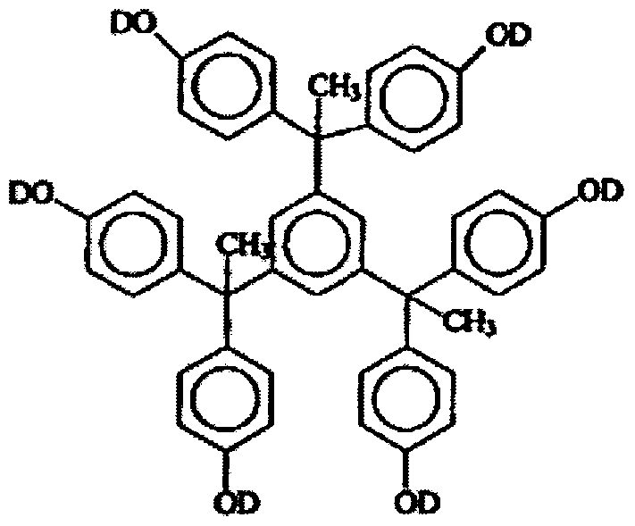


Claims
Priority Applications (2)
| Application Number | Priority Date | Filing Date | Title |
|---|---|---|---|
| US13/377,119 US20120088189A1 (en) | 2009-06-09 | 2010-06-04 | Conductive composition, transparent conductive film, display element and integrated solar battery |
| CN2010800259124A CN102804064A (en) | 2009-06-09 | 2010-06-04 | Conductive composition, transparent conductive film, display element and integrated solar battery |
Applications Claiming Priority (2)
| Application Number | Priority Date | Filing Date | Title |
|---|---|---|---|
| JP2009-138312 | 2009-06-09 | ||
| JP2009138312 | 2009-06-09 |
Publications (1)
| Publication Number | Publication Date |
|---|---|
| WO2010143701A1 true WO2010143701A1 (en) | 2010-12-16 |
Family
ID=43308956
Family Applications (1)
| Application Number | Title | Priority Date | Filing Date |
|---|---|---|---|
| PCT/JP2010/059890 Ceased WO2010143701A1 (en) | 2009-06-09 | 2010-06-04 | Conductive composition, transparent conductive film, display element and integrated solar battery |
Country Status (6)
| Country | Link |
|---|---|
| US (1) | US20120088189A1 (en) |
| JP (1) | JP2011018636A (en) |
| KR (1) | KR20120038438A (en) |
| CN (1) | CN102804064A (en) |
| TW (1) | TW201110147A (en) |
| WO (1) | WO2010143701A1 (en) |
Cited By (10)
| Publication number | Priority date | Publication date | Assignee | Title |
|---|---|---|---|---|
| CN102751381A (en) * | 2012-06-29 | 2012-10-24 | 中国科学院电工研究所 | Preparation method for copper indium selenium base film solar cell molybdenum electrode |
| WO2012161900A1 (en) * | 2011-05-23 | 2012-11-29 | Carestream Health, Inc. | Conductive composition comprising viscosity modifier |
| JP2013201007A (en) * | 2012-03-23 | 2013-10-03 | Fujifilm Corp | Conductive member and manufacturing method of the same, and touch panel |
| EP2720086A1 (en) * | 2012-10-12 | 2014-04-16 | Nano And Advanced Materials Institute Limited | Methods of fabricating transparent and nanomaterial-based conductive film |
| US20140205845A1 (en) * | 2013-01-18 | 2014-07-24 | Carestream Health, Inc. | Stabilization agents for transparent conductive films |
| EP2704156A4 (en) * | 2011-04-28 | 2014-10-08 | Fujifilm Corp | DISPERSION LIQUID CONTAINING METAL NANOWIRES, AND CONDUCTIVE FILM |
| US20150027755A1 (en) * | 2011-12-19 | 2015-01-29 | Panasonic Corporation | Transparent conductive film, substrate carrying transparent conductive film, and production method thereof |
| US9050775B2 (en) | 2012-10-12 | 2015-06-09 | Nano And Advanced Materials Institute Limited | Methods of fabricating transparent and nanomaterial-based conductive film |
| US20170088726A1 (en) * | 2010-02-05 | 2017-03-30 | Cam Holding Corporation | Photosensitive ink compositions and transparent conductors and method of using the same |
| KR20180044863A (en) * | 2018-04-20 | 2018-05-03 | 한국기계연구원 | Composition for coating transparent conductive film, transparent conductive film including coating layer formed by using the same, and electronic apparatus including coating layer formed by using the same |
Families Citing this family (44)
| Publication number | Priority date | Publication date | Assignee | Title |
|---|---|---|---|---|
| JP2009210871A (en) * | 2008-03-05 | 2009-09-17 | Toppan Printing Co Ltd | Colored application solution composition, color filter and liquid crystal display device |
| MY164919A (en) | 2009-09-11 | 2018-02-15 | First Solar Inc | Photovoltaic back contact |
| JP5301409B2 (en) * | 2009-10-05 | 2013-09-25 | 株式会社日本触媒 | Cationic curable resin composition and cured product thereof |
| JP2012009383A (en) * | 2010-06-28 | 2012-01-12 | Jnc Corp | Composition for coating formation, method of manufacturing substrate having patterned transparent conductive film obtained from the composition, and use of the manufactured body |
| JP2013016455A (en) * | 2011-01-13 | 2013-01-24 | Jnc Corp | Composition for coating formation used for formation of transparent conductive film |
| JP2012169072A (en) * | 2011-02-10 | 2012-09-06 | Fujifilm Corp | Laminate for forming conductive film, method of forming conductive film, conductive film, conductive element, touch panel and integrated solar cell |
| CN103732704A (en) * | 2011-05-18 | 2014-04-16 | 户田工业株式会社 | Method for producing conductive coating film and conductive coating film |
| JP2013008512A (en) * | 2011-06-23 | 2013-01-10 | Fujifilm Corp | Conductive composition, transparent conductor prepared using the same, and touch panel and solar cell including the transparent conductor |
| JP5888976B2 (en) | 2011-09-28 | 2016-03-22 | 富士フイルム株式会社 | Conductive composition, conductive member and method for producing the same, touch panel and solar cell |
| KR20140135718A (en) * | 2012-03-07 | 2014-11-26 | 스미토모 긴조쿠 고잔 가부시키가이샤 | Silver powder and method for producing same |
| US8586457B1 (en) * | 2012-05-17 | 2013-11-19 | Intermolecular, Inc. | Method of fabricating high efficiency CIGS solar cells |
| TWI490029B (en) * | 2012-07-20 | 2015-07-01 | Kern Energy Entpr Co Ltd | Gas recovering system |
| KR20140046923A (en) | 2012-10-11 | 2014-04-21 | 제일모직주식회사 | Transparent conductor, composition for manufacturing the same and optical display apparatus comprising the same |
| WO2014073597A1 (en) * | 2012-11-08 | 2014-05-15 | アルプス電気株式会社 | Conductor and method for producing same |
| JP6116285B2 (en) * | 2013-02-21 | 2017-04-19 | 太陽インキ製造株式会社 | Conductive resin composition and conductive circuit |
| CN103208561B (en) * | 2013-03-22 | 2016-04-20 | 中国科学院上海高等研究院 | A kind of flexible thin-film solar cell and preparation method thereof |
| KR101621282B1 (en) | 2013-09-13 | 2016-05-19 | 전자부품연구원 | Photosensitive coating solution and coated conductive film for transparent electrode using the same |
| WO2014157856A1 (en) * | 2013-03-25 | 2014-10-02 | 전자부품연구원 | Photosensitive coating composition, coating conductive film using photosensitive coating composition, and method for forming coating conductive film |
| KR101589546B1 (en) * | 2013-12-26 | 2016-01-29 | 전자부품연구원 | Transparent conductive film having improved visual clarity and preparation method thereof |
| KR101620037B1 (en) | 2013-12-27 | 2016-05-13 | 전자부품연구원 | Coating solution comprising metal nanowire, coated conductive film manufactured by using the same and preparation method thereof |
| KR101498187B1 (en) * | 2013-10-10 | 2015-03-04 | 전자부품연구원 | Photosensitive coating solution and coated conductive film for transparent electrode using the same |
| JP2015034279A (en) * | 2013-04-10 | 2015-02-19 | デクセリアルズ株式会社 | Ink composition for forming transparent conductive film, transparent conductive film, method for producing transparent electrode, and image display device |
| US9046224B2 (en) * | 2013-05-07 | 2015-06-02 | Technical Consumer Products, Inc. | LED lamp with controlled distribution |
| US20150000742A1 (en) * | 2013-07-01 | 2015-01-01 | Tsmc Solar Ltd. | Solar cell absorber thin film and method of fabricating same |
| TW201514802A (en) | 2013-07-16 | 2015-04-16 | Lg Innotek Co Ltd | Touch window and touch device including the same |
| CN105474096B (en) * | 2013-08-27 | 2019-11-12 | 日本瑞翁株式会社 | Radiation sensitive resin composition, resin film and electronic part |
| DE102013109386B3 (en) | 2013-08-29 | 2015-01-15 | Delfortgroup Ag | Efficiently produced cigarette paper for self-extinguishing cigarettes, process for its preparation and a cigarette |
| KR102117250B1 (en) * | 2013-09-23 | 2020-06-02 | 솔브레인 주식회사 | Composition for preparing transparent conductive layer and manufacturing method of transparent conductive structure using the same |
| KR101511060B1 (en) * | 2013-12-31 | 2015-04-13 | 주식회사 효성 | Bimetallic nanowire, preparing method of the same and transparent conductive film including the same |
| US9709887B2 (en) * | 2014-03-14 | 2017-07-18 | Hitachi Chemical Company, Ltd. | Photosensitive conductive film |
| KR102293227B1 (en) * | 2014-07-03 | 2021-08-23 | 동우 화인켐 주식회사 | Positive type composition and method for pattern formation of transparent conductors using the same |
| JP6384207B2 (en) * | 2014-09-01 | 2018-09-05 | 日油株式会社 | Silver-containing composition and silver element-forming substrate |
| TW201615764A (en) * | 2014-09-12 | 2016-05-01 | Idemitsu Kosan Co | Composition |
| WO2016093120A1 (en) * | 2014-12-08 | 2016-06-16 | 日東電工株式会社 | Transparent conductive film with adhesive layer |
| JP6890920B2 (en) * | 2014-12-08 | 2021-06-18 | 日東電工株式会社 | Transparent conductive film with adhesive layer |
| KR20170129883A (en) * | 2015-04-24 | 2017-11-27 | 코니카 미놀타 가부시키가이샤 | Transparent conductive film and method for producing transparent conductive film |
| CN105259715A (en) * | 2015-11-20 | 2016-01-20 | 深圳市华星光电技术有限公司 | Patterned electrode manufacturing method, liquid crystal display panel and liquid crystal display panel manufacturing method |
| CN106784393B (en) * | 2016-11-17 | 2019-06-04 | 昆山工研院新型平板显示技术中心有限公司 | A kind of conducting nanowires layer, graphic method and application |
| CN110494805A (en) * | 2017-03-13 | 2019-11-22 | 伊斯曼柯达公司 | Silver-containing compositions and uses containing cellulosic polymers |
| JP7043306B2 (en) * | 2018-03-23 | 2022-03-29 | 株式会社ノリタケカンパニーリミテド | Photosensitive compositions and their use |
| CN113185964B (en) * | 2021-03-15 | 2023-05-19 | 西北师范大学 | Preparation of an environmentally friendly ternary quantum dot material with super large Stokes shift |
| KR102686962B1 (en) * | 2022-01-27 | 2024-07-22 | 울산과학기술원 | Conductive composition, conductor, electrode and electronic device comprising the conductor |
| CN120152803A (en) * | 2023-01-17 | 2025-06-13 | 富士胶片株式会社 | Composition, conductive bonding material, device, and method for producing conductive bonding material |
| CN119314721A (en) * | 2024-10-15 | 2025-01-14 | 宁波维创柔性电子技术有限公司 | Electrode slurry for heterojunction solar cell and preparation method thereof |
Citations (2)
| Publication number | Priority date | Publication date | Assignee | Title |
|---|---|---|---|---|
| JP2007039567A (en) * | 2005-08-03 | 2007-02-15 | Kri Inc | COMPOSITE MOLDED ARTICLE FOR HIGH FREQUENCY ELECTRONIC COMPONENT AND COMPOSITION FOR PRODUCING COMPOSITE MOLDED ARTICLE FOR HIGH FREQUENCY ELECTRONIC COMPONENT |
| US20070074316A1 (en) * | 2005-08-12 | 2007-03-29 | Cambrios Technologies Corporation | Nanowires-based transparent conductors |
Family Cites Families (9)
| Publication number | Priority date | Publication date | Assignee | Title |
|---|---|---|---|---|
| JP3394938B2 (en) * | 1999-03-25 | 2003-04-07 | 株式会社村田製作所 | Photosensitive conductor paste |
| US6645695B2 (en) * | 2000-09-11 | 2003-11-11 | Shipley Company, L.L.C. | Photoresist composition |
| JP3614152B2 (en) * | 2001-08-07 | 2005-01-26 | 株式会社村田製作所 | Photosensitive conductive paste, circuit board using the same, and method for producing ceramic multilayer substrate |
| KR100965373B1 (en) * | 2003-06-10 | 2010-06-22 | 삼성전자주식회사 | Photosensitive metal nanoparticles and conductive pattern forming method using the same |
| US20050037278A1 (en) * | 2003-08-15 | 2005-02-17 | Jun Koishikawa | Photosensitive thick-film paste materials for forming light-transmitting electromagnetic shields, light-transmitting electromagnetic shields formed using the same, and method of manufacture thereof |
| KR100669725B1 (en) * | 2004-09-09 | 2007-01-16 | 삼성에스디아이 주식회사 | A photosensitive paste composition |
| CN100342064C (en) * | 2005-09-23 | 2007-10-10 | 浙江大学 | Silver nanometer wire synthesizing process |
| US20080292979A1 (en) * | 2007-05-22 | 2008-11-27 | Zhe Ding | Transparent conductive materials and coatings, methods of production and uses thereof |
| JP2009108407A (en) * | 2007-10-12 | 2009-05-21 | Fujifilm Corp | Bent rod-shaped metal particles, production method thereof, bent rod-shaped metal particle-containing composition, and conductive material |
-
2010
- 2010-05-31 JP JP2010124756A patent/JP2011018636A/en not_active Withdrawn
- 2010-06-04 CN CN2010800259124A patent/CN102804064A/en active Pending
- 2010-06-04 KR KR1020127000550A patent/KR20120038438A/en not_active Withdrawn
- 2010-06-04 US US13/377,119 patent/US20120088189A1/en not_active Abandoned
- 2010-06-04 WO PCT/JP2010/059890 patent/WO2010143701A1/en not_active Ceased
- 2010-06-09 TW TW099118745A patent/TW201110147A/en unknown
Patent Citations (2)
| Publication number | Priority date | Publication date | Assignee | Title |
|---|---|---|---|---|
| JP2007039567A (en) * | 2005-08-03 | 2007-02-15 | Kri Inc | COMPOSITE MOLDED ARTICLE FOR HIGH FREQUENCY ELECTRONIC COMPONENT AND COMPOSITION FOR PRODUCING COMPOSITE MOLDED ARTICLE FOR HIGH FREQUENCY ELECTRONIC COMPONENT |
| US20070074316A1 (en) * | 2005-08-12 | 2007-03-29 | Cambrios Technologies Corporation | Nanowires-based transparent conductors |
Cited By (12)
| Publication number | Priority date | Publication date | Assignee | Title |
|---|---|---|---|---|
| US20170088726A1 (en) * | 2010-02-05 | 2017-03-30 | Cam Holding Corporation | Photosensitive ink compositions and transparent conductors and method of using the same |
| US10550276B2 (en) * | 2010-02-05 | 2020-02-04 | Cambrios Film Solutions Corporation | Photosensitive ink compositions and transparent conductors and method of using the same |
| EP2704156A4 (en) * | 2011-04-28 | 2014-10-08 | Fujifilm Corp | DISPERSION LIQUID CONTAINING METAL NANOWIRES, AND CONDUCTIVE FILM |
| WO2012161900A1 (en) * | 2011-05-23 | 2012-11-29 | Carestream Health, Inc. | Conductive composition comprising viscosity modifier |
| US20150027755A1 (en) * | 2011-12-19 | 2015-01-29 | Panasonic Corporation | Transparent conductive film, substrate carrying transparent conductive film, and production method thereof |
| JP2013201007A (en) * | 2012-03-23 | 2013-10-03 | Fujifilm Corp | Conductive member and manufacturing method of the same, and touch panel |
| CN102751381A (en) * | 2012-06-29 | 2012-10-24 | 中国科学院电工研究所 | Preparation method for copper indium selenium base film solar cell molybdenum electrode |
| EP2720086A1 (en) * | 2012-10-12 | 2014-04-16 | Nano And Advanced Materials Institute Limited | Methods of fabricating transparent and nanomaterial-based conductive film |
| US9050775B2 (en) | 2012-10-12 | 2015-06-09 | Nano And Advanced Materials Institute Limited | Methods of fabricating transparent and nanomaterial-based conductive film |
| US20140205845A1 (en) * | 2013-01-18 | 2014-07-24 | Carestream Health, Inc. | Stabilization agents for transparent conductive films |
| KR20180044863A (en) * | 2018-04-20 | 2018-05-03 | 한국기계연구원 | Composition for coating transparent conductive film, transparent conductive film including coating layer formed by using the same, and electronic apparatus including coating layer formed by using the same |
| KR101939307B1 (en) | 2018-04-20 | 2019-01-16 | 한국기계연구원 | Composition for coating transparent conductive film, transparent conductive film including coating layer formed by using the same, and electronic apparatus including coating layer formed by using the same |
Also Published As
| Publication number | Publication date |
|---|---|
| JP2011018636A (en) | 2011-01-27 |
| TW201110147A (en) | 2011-03-16 |
| US20120088189A1 (en) | 2012-04-12 |
| KR20120038438A (en) | 2012-04-23 |
| CN102804064A (en) | 2012-11-28 |
Similar Documents
| Publication | Publication Date | Title |
|---|---|---|
| US20120088189A1 (en) | Conductive composition, transparent conductive film, display element and integrated solar battery | |
| US8298743B2 (en) | Positive-type photosensitive composition, transparent conductive film, display element and integrated solar battery | |
| US20100264378A1 (en) | Photosensitive composition, transparent conductive film, display element and integrated solar battery | |
| JP2012169072A (en) | Laminate for forming conductive film, method of forming conductive film, conductive film, conductive element, touch panel and integrated solar cell | |
| US20140203223A1 (en) | Conductive composition, method of producing the same, conductive member, touch panel, and solar cell | |
| KR101662417B1 (en) | Conductive composition, conductive member, conductive member manufacturing method, touch panel, and solar cell | |
| US8445097B2 (en) | Multi-layer fluoropolymeric film and articles incorporating such films | |
| DE69320725T2 (en) | Resin composition for sealing and a semiconductor device covered with sealing resin composition | |
| Obaid et al. | Preparation of chemically deposited thin films of CdS/PbS solar cell | |
| US8043800B2 (en) | Photosensitive material for forming conductive film, and conductive material | |
| KR101662418B1 (en) | Conductive composition, conductive member, conductive member manufacturing method, touch panel, and solar cell | |
| TW201303906A (en) | Conductive member, method of manufacturing the conductive member, touch panel, and solar cell | |
| KR101503043B1 (en) | A manufacturing method of absorption layer of thin film solar cell and thin film solar cell thereof | |
| CN103827978A (en) | Conductive composition, conductive member and manufacturing method thereof, touch panel, and solar cell | |
| WO2012147956A1 (en) | Conductive member, method for producing same, touch panel and solar cell | |
| WO2013090344A1 (en) | Electrically conductive polymeric compositons, contacts, assemblies, and methods | |
| CN101257058A (en) | Method and apparatus for fabricating solar panels with enhanced light harvesting | |
| US8362353B2 (en) | Photovoltaic module with multi-layer fluoropolymeric film | |
| US20220127459A1 (en) | Dielectric Film-Forming Composition | |
| JP2013225499A (en) | Conductive member, method for producing the same, touch panel, and solar cell | |
| DE102009054630B4 (en) | Method for producing a photovoltaic device | |
| JP2011082092A (en) | Patterned transparent conductive material, display element, and solar cell | |
| JP2013200997A (en) | Conductive member, manufacturing method therefor, and touch panel | |
| Brémaud | Investigation and development of CIGS solar cells on flexible substrates and with alternative electrical back contacts | |
| WO2019198536A1 (en) | Photovoltaic power generation system equipped with reflection mirror |
Legal Events
| Date | Code | Title | Description |
|---|---|---|---|
| WWE | Wipo information: entry into national phase |
Ref document number: 201080025912.4 Country of ref document: CN |
|
| 121 | Ep: the epo has been informed by wipo that ep was designated in this application |
Ref document number: 10786232 Country of ref document: EP Kind code of ref document: A1 |
|
| WWE | Wipo information: entry into national phase |
Ref document number: 13377119 Country of ref document: US |
|
| NENP | Non-entry into the national phase |
Ref country code: DE |
|
| ENP | Entry into the national phase |
Ref document number: 20127000550 Country of ref document: KR Kind code of ref document: A |
|
| 122 | Ep: pct application non-entry in european phase |
Ref document number: 10786232 Country of ref document: EP Kind code of ref document: A1 |