WO2010141115A2 - Directed material assembly - Google Patents
Directed material assembly Download PDFInfo
- Publication number
- WO2010141115A2 WO2010141115A2 PCT/US2010/024412 US2010024412W WO2010141115A2 WO 2010141115 A2 WO2010141115 A2 WO 2010141115A2 US 2010024412 W US2010024412 W US 2010024412W WO 2010141115 A2 WO2010141115 A2 WO 2010141115A2
- Authority
- WO
- WIPO (PCT)
- Prior art keywords
- group
- energy
- independently
- modified
- agent
- Prior art date
- Legal status (The legal status is an assumption and is not a legal conclusion. Google has not performed a legal analysis and makes no representation as to the accuracy of the status listed.)
- Ceased
Links
Classifications
-
- G—PHYSICS
- G03—PHOTOGRAPHY; CINEMATOGRAPHY; ANALOGOUS TECHNIQUES USING WAVES OTHER THAN OPTICAL WAVES; ELECTROGRAPHY; HOLOGRAPHY
- G03F—PHOTOMECHANICAL PRODUCTION OF TEXTURED OR PATTERNED SURFACES, e.g. FOR PRINTING, FOR PROCESSING OF SEMICONDUCTOR DEVICES; MATERIALS THEREFOR; ORIGINALS THEREFOR; APPARATUS SPECIALLY ADAPTED THEREFOR
- G03F7/00—Photomechanical, e.g. photolithographic, production of textured or patterned surfaces, e.g. printing surfaces; Materials therefor, e.g. comprising photoresists; Apparatus specially adapted therefor
- G03F7/16—Coating processes; Apparatus therefor
- G03F7/165—Monolayers, e.g. Langmuir-Blodgett
-
- B—PERFORMING OPERATIONS; TRANSPORTING
- B81—MICROSTRUCTURAL TECHNOLOGY
- B81C—PROCESSES OR APPARATUS SPECIALLY ADAPTED FOR THE MANUFACTURE OR TREATMENT OF MICROSTRUCTURAL DEVICES OR SYSTEMS
- B81C1/00—Manufacture or treatment of devices or systems in or on a substrate
- B81C1/00015—Manufacture or treatment of devices or systems in or on a substrate for manufacturing microsystems
- B81C1/00023—Manufacture or treatment of devices or systems in or on a substrate for manufacturing microsystems without movable or flexible elements
- B81C1/00031—Regular or irregular arrays of nanoscale structures, e.g. etch mask layer
-
- G—PHYSICS
- G03—PHOTOGRAPHY; CINEMATOGRAPHY; ANALOGOUS TECHNIQUES USING WAVES OTHER THAN OPTICAL WAVES; ELECTROGRAPHY; HOLOGRAPHY
- G03F—PHOTOMECHANICAL PRODUCTION OF TEXTURED OR PATTERNED SURFACES, e.g. FOR PRINTING, FOR PROCESSING OF SEMICONDUCTOR DEVICES; MATERIALS THEREFOR; ORIGINALS THEREFOR; APPARATUS SPECIALLY ADAPTED THEREFOR
- G03F7/00—Photomechanical, e.g. photolithographic, production of textured or patterned surfaces, e.g. printing surfaces; Materials therefor, e.g. comprising photoresists; Apparatus specially adapted therefor
- G03F7/004—Photosensitive materials
- G03F7/075—Silicon-containing compounds
- G03F7/0755—Non-macromolecular compounds containing Si-O, Si-C or Si-N bonds
-
- G—PHYSICS
- G03—PHOTOGRAPHY; CINEMATOGRAPHY; ANALOGOUS TECHNIQUES USING WAVES OTHER THAN OPTICAL WAVES; ELECTROGRAPHY; HOLOGRAPHY
- G03F—PHOTOMECHANICAL PRODUCTION OF TEXTURED OR PATTERNED SURFACES, e.g. FOR PRINTING, FOR PROCESSING OF SEMICONDUCTOR DEVICES; MATERIALS THEREFOR; ORIGINALS THEREFOR; APPARATUS SPECIALLY ADAPTED THEREFOR
- G03F7/00—Photomechanical, e.g. photolithographic, production of textured or patterned surfaces, e.g. printing surfaces; Materials therefor, e.g. comprising photoresists; Apparatus specially adapted therefor
- G03F7/26—Processing photosensitive materials; Apparatus therefor
- G03F7/265—Selective reaction with inorganic or organometallic reagents after image-wise exposure, e.g. silylation
-
- H—ELECTRICITY
- H10—SEMICONDUCTOR DEVICES; ELECTRIC SOLID-STATE DEVICES NOT OTHERWISE PROVIDED FOR
- H10P—GENERIC PROCESSES OR APPARATUS FOR THE MANUFACTURE OR TREATMENT OF DEVICES COVERED BY CLASS H10
- H10P76/00—Manufacture or treatment of masks on semiconductor bodies, e.g. by lithography or photolithography
- H10P76/40—Manufacture or treatment of masks on semiconductor bodies, e.g. by lithography or photolithography of masks comprising inorganic materials
- H10P76/408—Manufacture or treatment of masks on semiconductor bodies, e.g. by lithography or photolithography of masks comprising inorganic materials characterised by their sizes, orientations, dispositions, behaviours or shapes
- H10P76/4085—Manufacture or treatment of masks on semiconductor bodies, e.g. by lithography or photolithography of masks comprising inorganic materials characterised by their sizes, orientations, dispositions, behaviours or shapes characterised by the processes involved to create the masks
-
- B—PERFORMING OPERATIONS; TRANSPORTING
- B81—MICROSTRUCTURAL TECHNOLOGY
- B81C—PROCESSES OR APPARATUS SPECIALLY ADAPTED FOR THE MANUFACTURE OR TREATMENT OF MICROSTRUCTURAL DEVICES OR SYSTEMS
- B81C2201/00—Manufacture or treatment of microstructural devices or systems
- B81C2201/01—Manufacture or treatment of microstructural devices or systems in or on a substrate
- B81C2201/0101—Shaping material; Structuring the bulk substrate or layers on the substrate; Film patterning
- B81C2201/0147—Film patterning
- B81C2201/0149—Forming nanoscale microstructures using auto-arranging or self-assembling material
-
- B—PERFORMING OPERATIONS; TRANSPORTING
- B81—MICROSTRUCTURAL TECHNOLOGY
- B81C—PROCESSES OR APPARATUS SPECIALLY ADAPTED FOR THE MANUFACTURE OR TREATMENT OF MICROSTRUCTURAL DEVICES OR SYSTEMS
- B81C2201/00—Manufacture or treatment of microstructural devices or systems
- B81C2201/01—Manufacture or treatment of microstructural devices or systems in or on a substrate
- B81C2201/0198—Manufacture or treatment of microstructural devices or systems in or on a substrate for making a masking layer
-
- Y—GENERAL TAGGING OF NEW TECHNOLOGICAL DEVELOPMENTS; GENERAL TAGGING OF CROSS-SECTIONAL TECHNOLOGIES SPANNING OVER SEVERAL SECTIONS OF THE IPC; TECHNICAL SUBJECTS COVERED BY FORMER USPC CROSS-REFERENCE ART COLLECTIONS [XRACs] AND DIGESTS
- Y10—TECHNICAL SUBJECTS COVERED BY FORMER USPC
- Y10T—TECHNICAL SUBJECTS COVERED BY FORMER US CLASSIFICATION
- Y10T428/00—Stock material or miscellaneous articles
- Y10T428/24—Structurally defined web or sheet [e.g., overall dimension, etc.]
- Y10T428/24174—Structurally defined web or sheet [e.g., overall dimension, etc.] including sheet or component perpendicular to plane of web or sheet
-
- Y—GENERAL TAGGING OF NEW TECHNOLOGICAL DEVELOPMENTS; GENERAL TAGGING OF CROSS-SECTIONAL TECHNOLOGIES SPANNING OVER SEVERAL SECTIONS OF THE IPC; TECHNICAL SUBJECTS COVERED BY FORMER USPC CROSS-REFERENCE ART COLLECTIONS [XRACs] AND DIGESTS
- Y10—TECHNICAL SUBJECTS COVERED BY FORMER USPC
- Y10T—TECHNICAL SUBJECTS COVERED BY FORMER US CLASSIFICATION
- Y10T428/00—Stock material or miscellaneous articles
- Y10T428/24—Structurally defined web or sheet [e.g., overall dimension, etc.]
- Y10T428/24479—Structurally defined web or sheet [e.g., overall dimension, etc.] including variation in thickness
- Y10T428/24612—Composite web or sheet
Definitions
- the present application relates to directing assembly of materials, including preparing substrates to perform directed assembly thereon.
- Optical lithography at UV wavelengths is the standard process for patterning 65- nm state-of-the-art devices in the semiconductor industry, and extensions to 32-nm and below are currently being explored.
- Advanced lithographic schemes are focused on the use of short wavelength (193 nm or 157 nm), coupled with immersion to further reduce the effective wavelength.
- Alternate approaches employ higher energy actinic radiation such as extreme ultraviolet (EUV) at 14.4 nm or high voltage electron beams to further improve lithographic resolution.
- EUV extreme ultraviolet
- Mass-produced semiconductor manufacturing entered the era on nanopatterning with UV optical lithography when the smallest feature sizes crossed the 100-nm threshold.
- advanced devices have had their half-pitch at 65 nm using 193-nm dry exposures, and it is widely expected to extend to 45-nm half-pitch by incorporating liquid immersion.
- IRS international roadmap for semiconductors
- a modified surface is created on a substrate by applying a first surface agent to the substrate.
- Energy is applied to the modified surface to form an imaged surface having an imaged portion and a non-imaged portion.
- the imaged portion is characterized by a surface energy that is different from the surface energy of the non-imaged portion.
- the applied energy can remove at least a portion of an attached surface agent from the imaged portion to modify the surface energy.
- the energy also modifies the surface agent without causing oxidation.
- the surface modification and/or energy application can take place in a low oxygen environment (e.g., having an oxygen content lower than that present in about 0.01 Torr of air).
- the imaged surface can then be exposed to a self assembling material, such as a block copolymer, such that the surface can direct assembly of the self assembling material by preferential attachment of certain moieties of the block copolymer to imaged or non-imaged portions of the surface in order to form a selected pattern.
- a self assembling material such as a block copolymer
- a second surface agent can be applied to the imaged and non-imaged portions of the modified surface, where the second surface agent can preferentially adhere to either the imaged or non-imaged portion creating another surface energy.
- energy can be applied on at least a portion of the surface having the second surface agent, which can create yet another surface energy.
- Additional surface agents can also be applied, optionally with additional exposures of energy, to further define the selected pattern.
- the selected pattern can have a number of different characteristics. In some instances, the selected pattern is based upon at least one of the energy of the imaged portion and the energy of the non-imaged portion. The selected pattern can correspond with at least one of the imaged portion and the non-imaged portion.
- the selected pattern formed by the self assembling material can exhibit a first pitch and the second surface agent applied to the modified surface can exhibit a second pitch, where the second pitch is larger than the first pitch.
- the selected pattern can exhibit a substantially uniform block copolymer morphology.
- the selected pattern can exhibit a selected defect number density (e.g., lower than about one per square micrometer).
- the block copolymer can exhibit a structure having an axis of symmetry oriented substantially perpendicular to a surface of the substrate. Such structures can include lamellae and/or cylinders.
- the types of energy that can be applied on a surface modified material can include any form suitable for directing self assembly of a material.
- the energy can be in the form of x-rays, EUV, or radiation exhibiting at least one wavelength greater than about 140 nm. In some instances, the energy can be characterized by a wavelength greater than about 190 nm (e.g., about 193 nm or about 248 nm). In such cases, it can be advantageous to utilize a surface agent that includes an aryl group - though such groups may also be advantageous when other energy forms are utilized.
- a silicon-containing agent can include any number of organic moieties, such as aryl entities and/or substituted aliphatic entities.
- a silicon-containing agent can include a portion consistent with at least one of the following structural formulas:
- R2 and R3 are each independently any one of F, Cl, Br, I, OH, OM, OR, R, NR 2 , SiR 3 , NCO, CN, or OCOR;
- M is a metal atom
- X is either NR or O
- n is an integer having a value of 1 or greater
- each Q is independently any one of O, NR, SiR 2 , (O)CO, (N)CO, PR, POR, S, SS, SO 2 , or SO 3
- each R is independently any one of an alkyl group, a vinyl group, an aryl group, a hydrogen, a haloalkyl group, a halovinyl group, or a haloaryl group
- each Y is independently any one of an alkyl group, a vinyl group, an aryl group ,a silane, a siloxane, a haloalkyl group, a halovinyl group, or a haloaryl group
- each Z is independently any one of F, Cl, Br, I, OH, OM, OR, R, NR 2 , SiR 3 ,
- NCO NCO
- CN OCOR, NCOR
- PR 2 PROR
- P(OR) 2 P(OR) 2
- SR SSR
- SO 2 R SO 3 R.
- energy can remove at least a portion of the agent by breaking the bond between the silicon atom and another atom.
- the portion of a surface agent that is removed can include any of R2, R3, (Z-Y), (Z-[Z-Y] n ), and (Z-Y-[Q-Y] n ).
- Other embodiments are directed to self assembling structures, which in some instances can be formed using various of the techniques disclosed herein. Such structures can include a substrate having a surface modified by a surface agent. Any of the surface agents described herein can be utilized.
- the modified surface can imaged portions and non-imaged portions, the imaged portions characterized by a first surface energy and the non-imaged portions characterized by a second surface energy.
- the modified surface can include three or more different surface energies.
- a block copolymer, or other self assembling material can be assembled on the substrate to form a selected pattern based upon at least one of the first surface energy and the second surface energy. The selected pattern exhibiting a defect number density lower than about 1 per square micrometer, and/or include any combination of the features previously described.
- FIG. 1 depicts a flow diagram of three processes for directing assembly of self assembling materials, in accord with some embodiments of the present invention
- FIG. 2 is a schematic of a graph of dose against lateral position from conventional lithographic radiation, and a corresponding change in hydrophobicity of a material as a function of lithographic radiation dosage in accord with some embodiments of the present invention
- FIG. 3 is a schematic of the assembling of diblock copolymers on a densely patterned surface, in accord with some embodiments of the present invention
- FIG. 4 is a schematic of the assembling of diblock copolymers on a sparsely patterned surface, in accord with some embodiments of the present invention
- FIG. 5 is a schematic comparing the assembling of diblock copolymers on densely and sparsely patterned surfaces, in accord with some embodiments of the present invention.
- FIG. 6 presents some scanning electron microscopy (“SEM”) images of poly(styrene-block-methyl methacrylate) (“P(S-b-MMA)”) film on patterned 11 BuSiCl 3 , the self assembling monolayer (“SAM”) showing examples of classes of defects in Wafer 9D and examples of low or zero defects on the remaining SEM images, in accord with some embodiments of the present invention.
- SEM scanning electron microscopy
- Some techniques utilize surface agents (e.g., non-polymeric materials), which can be exposed to a pattern of energy to create a plural energetic surface. Materials capable of self assembly, such as block copolymers, can then be contacted with the plural energetic surface. The characteristics of the plural energetic surface and the block copolymers, can lead to self assembly of the block copolymers on the surface, resulting in a selected pattern.
- surface agents e.g., non-polymeric materials
- such methods and compositions can aid in the formation of structures (e.g., features having sizes in a range from about 1 nm to about 1 micrometer) on a substrate without the need for applying, lithographically imaging, and developing typical organic resist materials.
- the self assembled pattern can result in patterns with very low defect densities and/or uniform block copolymer conformations with in a selected portion of a pattern.
- resistless techniques for directing self assembly of materials can accrue several potential advantages.
- the current industry consensus on lithography exposure tool potential solutions for patterning through the 16 nm DRAM half-pitch node suggests that EUV and innovative 193 nm optical immersion technologies will dominate between the 32 nm and the 22 nm technology nodes.
- Lithographically directed self assembly has two potential large advantages over traditional resist based lithography.
- One advantage is that the resolution is defined by the thermodynamic properties of the self assembling material, and not the chemistry of the resist.
- the type and molecular weight of the polymer blocks, for example, are the only resolution defining properties of the material. These properties can be manipulated to give sub-10 nm patterning.
- the factors that limit traditional resist resolution and LWR such as polymer molecular weight, acid diffusion, and photoacid generator segregation are not present in self assembly.
- a second advantage is that traditional resist based lithography is not employed to define the pattern.
- Traditional directed self assembly employs a resist to define the initial pattern and is thus limited by all the constraints of resist based lithography.
- Our approach employs a resist-less imaging layer comprised of a monolayer of a surface modifying layer. This ultra thin film is used to direct the final block polymer assembly through changes in surface polarity or other surface properties.
- the ability to direct polymer assembly without the need of a resist step also removes the need for additional processing steps such as additional film deposition or plasma etch based transfer steps. This reduction in processing steps should act to increase chip yield due to defect reduction and reducing manufacturing cost due to reduced processing steps.
- a final, and perhaps biggest advantage, is that is may not be possible to produce sub-22 nm based integrated circuits without the use of a directed self-assembly either as a stand alone technology or coupled into a grid-based dual-patterning scheme. It is likely that potential cost advantages of this technology along with improved lithographic performance will make this technology the choice for advanced sub-22 nanometer lithography.
- Directed self assembly may be coupled with an advanced lithography scheme such as immersion 193-nm or EUV lithography or maskless electron beam in a dual exposure process. The dual exposure process would employ directed self assembly to form a grid pattern and then follow this with a second exposure to define the final resist pattern.
- This dual exposure grid based approach is heavily favored by many companies as the best route to sub-22 nanometer lithography. It is also likely that by employing a polymer solution containing both a block polymer and a homopolymer that sub-22 nm imaging can be performed as a single lithography step. This used of this technology may be most appropriate for leading edge sub-22 nm lithography followed by full scale manufacturing at the sub- 16 nm lithography and continuing on to the end the lithographic roadmap.
- Block polymers are one set of self- assembling materials that are currently being developed for patterning and other applications in nanofabrication.
- Block copolymers typically comprise two or more chemically different polymer chains connected by a covalent bond.
- Self assembling materials when exposed to particular environments, tend to spontaneously form ordered structures at the molecular scale, which can have domain dimensions of about 1 nm to about 1 ⁇ m. The morphology and the size of the domains are dependent on the molecular weight and composition of the copolymer and can assume geometries such as spheres, cylinders, and lamellae.
- Block copolymers have been used in demonstrations of nanofabrication because they microphase separate to form ordered, chemically distinct domains with dimensions of between 5-50 nm.
- the size and shape of these domains can be controlled by manipulating the molecular weight and composition of the copolymer (e.g., the molecular weight of one or more of the blocks of a block copolymer).
- An advantage of using block copolymer systems is that linewidth and line width roughness are dictated by thermodynamics of interaction both within the block copolymer and between the copolymer and the substrate surface.
- One approach to employing block copolymers in nanofabrication is to employ resist-based lithographic techniques to define differentiated surface chemistries on a surface followed by self-assembly of the block copolymer film on the patterned surface.
- resist-based lithographic techniques to define differentiated surface chemistries on a surface followed by self-assembly of the block copolymer film on the patterned surface.
- a in FIG. 1 A resist is first coated 1 10 onto a hydrophobic organic material covering a hydrophilic inorganic material (e.g., a silicon wafer). The resist is then imaged 120 with energy to form a pattern thereon.
- Traditional resists have been patterned by a variety of advanced imaging systems employing different DUV wavelengths, EUV, X-ray, electron beams, and ion beams.
- the imaged resist can then be processed 130 (e.g., developed) to provide an initial lithographic pattern.
- This pattern can then transferred 140 into the underlying hydrophilic inorganic substrate, e.g., by using one or more plasma etch steps.
- the resist is finally removed 150 to uncover the hydrophobic organic material.
- the resulting surface is a mixture of areas of hydrophobic organic material and hydrophilic inorganic material whose pattern has been lithographically defined by a plurality of different surface energies.
- the difference in surface hydrophobicity is used to direct the self assembly of block copolymers 160, which are applied to the surface.
- the differences in energies serve as a template to direct self assembly of the block copolymers.
- a thin film of a diblock copolymer can be deposited on the patterned imaging layer and annealed above the glass transition temperature of the blocks of the copolymer.
- the copolymer film can self assembly into lamellar domains such that adjacent regions of the chemically patterned surface are preferentially attracted to different blocks of the copolymer.
- the lamellae can orient and amplify the surface pattern.
- selective removal of one of the blocks can optionally be performed, resulting in a nanopatterned template that can be used in nanofabrication.
- the preferential attraction is a result of several types of interactions that exist at the interface of the surface and the polymer. These intermolecular interactions as known as Lifshitz-Van der Walls interactions and can include three different interactions: London's dispersive interactions, Keeson's dipole-dipole interactions, and Debye's interactions. Additional interactions can also be present such as hydrogen bonding and
- Lewis acid-base interactions A method to quantify some of these interactions is by the measurement of surface free energy of the material and polymer surfaces.
- the free energy can be differentiated into polar and dispersive free energies and the polar free energy can be further differentiated into acidic and basic components. It is the matching of the varies components of surface free energy between the differentiated material surfaces and the different polymer blocks that lead to directed self assembly.
- the interactions between an imaged surface (e.g., the energy of the imaged surface) and the self assembling material (e.g., block copolymer) can aid in determining how the material orients on the surface. As described in the present application, many copolymers can orient as lamellae layers.
- an imaged layer can tend to direct assembly of material such that the material exhibits an axis of symmetry which is substantially perpendicular to the imaged surface. Accordingly, for example, a copolymer can orient as cylinders each with an axis substantially perpendicular to the imaged surface.
- Lamallae can also be oriented, where the cross section of the lamellae (e.g., parallel to the imaged surface) can exhibit any number of shapes (e.g., triangular, square, rectangular, hexagonal, etc.). Examples of such orientations are discussed in Bates, F. S. et al., "Block Copolymers - Designer Soft Materials," Physics Today, February 1999, pp. 32-38, which is hereby incorporated herein by reference in its entirety.
- Some embodiments of the present invention are directed to processes that prepare surfaces with multiple surface energies that can be used to direct a self- assembling material to conform to a selected pattern. Such processes can eliminate the need for resist processing by allowing direct imaging of a modified surface, without requiring subsequent surface modification, deposition, or plasma etch steps. Accordingly, such processes can result in higher resolution templates that can direct assembly of materials such as block copolymers in a manner to achieve lower defect densities, and/or reduce the labor associated with preparing template surfaces.
- Some exemplary embodiments are described with respect to FIG. 1, and the flow chart labeled Process B. An example is shown in Figure 1 where an inorganic surface is modified 1 1 1 through the used of a surface agent.
- the modified surface in which the surface agent can be attached to the surface, is characterized by a first surface energy.
- the modified surface can be imaged 121 by applying energy on the modified surface to form one or more imaged portions and one or more non-imaged portions.
- the imaged portions can be characterized by a second surface energy, which can be different from the first surface energy.
- a material capable of self assembly e.g., a block copolymer
- This step can be performed without further processing of the imaged modified surface (e.g., need for further processing the surface agent).
- the approach of Process B is not limited by conventional lithographic patterning of a resist imaging layer and significantly reduces manufacturing processing steps.
- the resist is chemically changed by exposure to light with the degree of change proportional to the light intensity.
- the lithographic aerial image near the resolution limit is a sinusoidal intensity pattern and the time integrated intensity pattern is the spatial distribution of applied dose. This is shown as the sinusoidal line 210 in FIG. 2.
- the resist will change properties from being normally base insoluble to base soluble. This will result resist loss in the exposed areas and resist retention in the unexposed areas leading to pattern formation on the underlying substrate.
- this pattern is transferred into a hydrophilic inorganic material and then the resist is removed to uncover the hydrophobic organic material leading to two distinct and different surfaces. This method gives a binary surface in terms of hydrophobicity, either hydrophobic organic or hydrophilic inorganic.
- a surface is transformed directly in the lithography step with no further processing.
- An example is shown in FIG. 2 where the surface hydrophobicity is inversely proportional to the exposure dose.
- the normally hydrophobic surface remains hydrophobic and in areas of high dose 220 the surface is changed to hydrophilic.
- the surface In areas of intermediate dose 230, the surface will exhibit an intermediate increase in its hydrophilic character.
- This method can yield a continuous surface in terms of hydrophobicity, in which the degree of hydrophobicity follows the aerial image intensity.
- FIG. 3 A schematic diagram of surface self-assembly using a sinusoidal continuously varying surface character, consistent with a particular embodiment, is shown in FIG. 3.
- the initially hydrophobic surface 310 can be lithographically transformed to a surface containing regions of from hydrophobic 315, intermediate 325, and hydrophilic 335 polarity.
- a block polymer 340 containing both hydrophobic 342 and hydrophilic chains 341, or other appropriate self-assembling material, is introduced to the surface and directed to assemble on their like polarity surface.
- the hydrophobic surface 315 directs assembly of the hydrophobic chain 342 of the polymer while the hydrophilic surface 335 directs assembly of the hydrophilic chain 341 of the polymer.
- the surface with intermediate polarity 325 is not expected to direct assembly and is considered neutral in its directing ability.
- a potential advantage of continuous surface assembly is that sufficiently directing ability is present in the hydrophobic and hydrophilic regions to remove the necessary of additional processing steps to give a binary surface with distinct hydrophobic and hydrophilic regions.
- a selected pattern of the self-assembled material can be substantially similar to the pattern imaged on the substrate surface by different energies.
- a surface can imaged using a pattern that repeats a selected number of times, where the pattern repetition is characterized by an imaged pitch.
- a subsequently self assembled material on the imaged surface can also exhibit a repeating pattern, where the assembled pattern is characterized by a assembled pitch.
- the assembled pitch is smaller than the imaged pitch. Accordingly, the self assembled material can potentially exhibit smaller spatial resolution in terms of its repeated pattern relative to the imaged self assembling surface. It should be understood that the term "pitch" need not limit a repeating pattern to patterns that exhibit spatial symmetry.
- an imaged surface energy pattern can be characterized by two alternating regions having different surface energies, where one region is larger than another.
- the pitch is the sum of the size of both regions.
- a pitch can also refer to energy regions that are identical in extent as well.
- FIG. 4 A schematic diagram of surface self-assembly using a non-sinusoidal varying surface character, consistent with a particular embodiment, is shown in FIG. 4.
- the initially hydrophobic surface 410 can be lithographically transformed to a surface containing regions of from intermediate 425 and hydrophilic 435 polarity.
- a block polymer 440 containing both hydrophobic 441 and hydrophilic 442 chains, or other appropriate self-assembling material, is introduced to the surface and directed to assemble on their like polarity surface.
- the hydrophilic surface 435 directs assembly of the hydrophilic chain 442 of the polymer.
- the surface with intermediate polarity 425 is not expected to direct assembly and is considered neutral in its directing ability.
- a potential advantage of this embodiment is the ability to frequency multiply the amount of assembled lines relative to the amount of lithography written lines with the potential to increase the resolution of assembly by writing one line in a given pitch and assembling more them one line in that same pitch. This advantage would be especially useful when employing conventional electron beam lithography where the writing time is directly proportional to the amount of pattern being written, and/or in optical lithography when printing near the resolution limit can degrade densely written aerial imagines more then sparsely written aerial images.
- FIG. 5 shows a schematic of the directed self-assembly on dense 500 and sparse 505 chemical patterns, which can be written by e-beam lithography.
- the substrate pitch Ps
- the substrate pitch is approximately that of the lamellar spacing
- the pinning line is the feature written that is preferential to one of the blocks and directs the self-assembly of the block copolymer film (e.g., the pinning line 510 can attract a polymethyl methacrylate block 515 with the other line 520 attracting a polystyrene block 525). In the embodiments consistent with FIG. 5, Wp can exhibit a thickness of about 0.5 Lo.
- one of the blocks can be removed giving a three dimensional feature similar to that obtained with conventional resist lithography.
- This feature can be used as a conventional resist for post lithographic processing such as masking for ion implant for doping or masking for etch or plasma etch to transfer periodic lines into the underlying substrate.
- additional surface modifications can be employed to direct self assembly of materials.
- An example of such a process is depicted as Process C in FIG. 1.
- processes can employ two or more surface modification steps, and can also employ two or more resistless lithography steps (as shown in Process C), that directly change the surface energy without requiring deposition and/or plasma etch steps.
- the initial surface modification 1 15 followed by imaging 125 gives one surface differentiated from the initial surface by any number of material surface properties.
- a second surface modification step 135 can then be employed to convert the exposed region to a third surface different from at least one of the first and second by type of surface energies or any number of by any number of other material surface properties.
- the surface modified by the second surface modification can be optionally further exposed 145 to give a third surface similar to that of the first exposed surface.
- the result of the double surface modification and imaging approach is that as many as three different surfaces are lithography defined on the original material surface and as such a surface more prone to directed self assembly is created. Indeed, more complicated patterns and more complicated self assembling materials (e.g., triblock copolymers) can be utilized to yield a richer space of achievable structures.
- the second surface modifying agent is then employed to modify only the image area leading to a surface containing two new surfaces different from the original and capable of improved directed self assembly. It is understood that embodiments of the invention are not limited to two sequences of surface modification followed imaging steps. It is possible that three or more sequences of surface modification, followed optionally by imaging steps, can be employed to give multiple surfaces on a material surface capable of further improved directed self assembly. The final imaging step is still considered optional in any sequence of three or more surface modification and imaging steps.
- a variety of base substrates can be utilized having numerous types of surfaces can optionally be used.
- Non-limiting examples can include a silicon wafer or quartz wafer of a glass slide.
- surface agents can be embodied as surface labile moieties such a photoelectron-labile, or ion labile moiety that can be at least partially selectively removed upon exposure.
- removal of at least a portion of a surface agent is meant to denote that at least a fragment of an attached surface agent is removed as a result of energy exposure.
- the removal of at least a portion of a surface labile moiety can cause a change in surface properties, such as surface polarity or surface energy or the acid-base properties of the surface, such that different surface states exist on the surface of the substrate.
- These states can be the original surface modifying material or a fragment of the surface agent material or the originally unmodified surface.
- the fragment of the surface agent material may be partially the original surface in the case where the energy results in removal of the surface modifying material and regenerates the original surface.
- the original and transformed surfaces will have sufficiently different surface polarity or other material properties such to direct the assembly of materials to the surface to where the different attractive forces of material to be assembled will be compatible with different attractive forces of the surface.
- some embodiments are directed to methods and materials, which involve self-assembling structures having a defect number density below a threshold value.
- the threshold value can be about 10/ ⁇ m 2 , 1/ ⁇ m 2 , 0.1/ ⁇ m 2 , 0.01/ ⁇ m 2 , 0.001/ ⁇ m 2 , or lower.
- any material having suitable properties consistent with embodiments of the present invention can be utilized as a surface modifying agent.
- Such agents can be polymeric in nature, or non-polymeric (e.g., having a plurality of repeat units of 20 or fewer.
- the surface modifying agent is capable of attaching to a substrate surface (or other entity) by way of a covalent bond.
- other surface agents may attach using any number of other mechanisms (e.g., ionic bonding, van der Waals forces, hydrogen bonding, etc).
- surface modifying agents can include silicon-containing agents, which can be silicon based coupling materials such as aryl or alkyl substituted silanols, silyl alkanols, and silyl halides.
- the use of energy can be such as to sever at least one bond between a silicon atom and at least one connected moiety to cause the agent to be removed. In some particular embodiments, this is distinct from situations where energy application results in conversion of a moiety connected to the silicon atom (e.g., the energy does not cause a bond between a silicon atom and another atom to break).
- One aspect of the invention is to take a silicon-containing surface modifying agent as shown in Structural Formula I(a) and modify the surface of a substrate to form the bound material shown in Structural Formula I(b).
- the surface of a substrate can be modified with any number and any degree of surface modifying agents.
- the surface can also be modified with more than one type of surface modifying agent by attaching the agents either sequentially or concurrently. In some aspects of this invention, it can be advantageous to modify the surface with more than one type of surface modifying agent.
- Rl F, Cl, Br, I, OH, OM, OR, R, NR 2 , SiR 3 , NCO, CN, OCOR
- R2 F, Cl, Br, I, OH, OM, OR, R, NR 2 , SiR 3 , NCO, CN, OCOR
- R3 F, Cl, Br, I, OH, OM, OR, R, NR 2 , SiR 3 , NCO, CN, OCOR
- R alkyl, cycloalkyl, vinyl, aromatic, hydrogen, haloalkyl, halovinyl, haloaromatic
- Y alkyl, cycloalkyl, vinyl, aromatic, silanes, siloxanes, haloalkyl, halovinyl, haloaromatic
- Z F, Cl, Br, I, OH, OM, OR, R, NR 2 , SiR 3 , NCO, CN, OCOR, NCOR, PR 2 , PROR,
- the exemplary structure I(b) depicts the attachment between the silicon containing surface modifying agent and the surface to occur at only one point. It is well known to those skilled in the art that attachment can occur at through the displacement of Rl, R2, or R3 including any combination of Rl, R2, or R3, to give two or three attachment points between the silicon containing surface modifying agent and the particle. It is also well known to those skilled in the art that attachment can occur at through the displacement of the Rl, R2, or R3 of one silicon containing surface modifying agent and a second silicon containing surface modifying agent previously attached to the particle. Any form of attachment of the silicon containing surface modifying agent to the particle is acceptable to the practice of this invention.
- the surface modifying agents shown in Structural Formulas I(a) and I(b) contain a coupling region containing a silicon atom bonded to at least one hydrolyzable moiety, optionally a spacer region shown as Y, and an active region shown as Z. If no spacer region is employed, Z can be directly attached to the silicon.
- the silicon is also typically substituted with three groups designated as Rl, R2, and R3 which can be identical or different provided that one group is hydrolyzable during the surface modification reaction. Hydrolyzable groups can be, but are not limited to, H, F, Cl, Br, I, OH, OM, OR, NR 2 , SiR 3 , NCO, and OCOR.
- the spacer region Y is typically an alkyl, vinyl, aromatic silane, or siloxane- based organic moiety which can optionally be substituted with other organic moieties such as acyl halide, alcohol, aldehyde, alkane, alkene, alkyne, amide, amine, arene, heteroarene, azide, carboxylic acid, disulfide, epoxide, ester, ether, halide, ketone, nitrile, nitro, phenol, sulfide, sulfone, sulfonic acid, sulfoxide, silane, siloxane or thiol.
- acyl halide alcohol, aldehyde, alkane, alkene, alkyne, amide, amine, arene, heteroarene, azide, carboxylic acid, disulfide, epoxide, ester, ether, halide, ketone, nitrile, nitro
- the alkyl, vinyl, or aromatic based organic moiety may contain up to 50 carbon atoms, and contains more preferably up to 20 carbon atoms, and contains most preferably up to 10 carbon atoms.
- the silane or siloxane-based silicon moiety may contain up to 50 silicon or carbon atoms, and contains more preferably up to 20 silicon or carbon atoms, and contains most preferably up to 10 silicon or carbon atoms.
- Attached to the Y spacer region, or optionally directly to the silicon, is the active region shown as Z.
- the active region can be employed to attract and bind the molecule of interest. In the case of a diblock polymer, this region will act to attract and bind the region of the polymer in which in shares a similar polarity or other form of surface attraction.
- the binding can be but is not limited to van der Waals interactions, hydrogen bonding, covalent bounding, and ionic bonding.
- the active region can also contain an alkyl, vinyl, or aromatic based organic moiety which may be substituted with other organic moieties such as acyl halide, alcohol, aldehyde, alkane, alkene, alkyne, amide, amine, arene, heteroarene, azide, carboxylic acid, disulfide, epoxide, ester, ether, halide, ketone, nitrile, nitro, phenol, sulfide, sulfone, sulfonic acid, sulfoxide, silane, siloxane or thiol.
- the alkyl, vinyl, or aromatic based organic moiety may contain up to 50 carbon atoms, and contains more preferably up to 20 carbon atoms, and contains most preferably up to 10 carbon atoms.
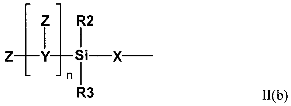
- aspects of the invention utilize a silicon containing surface modifying agent shown in Structural Formulas II(a) and I ⁇ I(a) and modify the surface of a material to give the material represented in Structural Formulas II(b) and I ⁇ I(b), respectively.
- the potential identities of Rl, R2, R3, X. Y, and Z are the same as delineated previously.
- the number of active regions in the surface modifying agent is more than one with each separated by spacer region. It is recognized that when more than one active region is employed on the surface modifying agent that the active regions can be attached in either a linear manner or in a branched manner from the space region.
- n in Structural Formulas II(a)(b) and III(a)(b) should be 1 or greater (e.g., corresponding with the number of active regions desired).
- Rl F, Cl, Br, I, OH, OM, OR, R, NR 2 , SiR 3 , NCO, CN, OCOR
- R alkyl, cycloalkyl, vinyl, aromatic, hydrogen, haloalkyl, halovinyl, haloaromatic
- Y alkyl, cycloalkyl, vinyl, aromatic, silanes, siloxanes, haloalkyl, halovinyl, haloaromatic
- the active regions on a surface modifying agent can be the same or different, and the spacer regions on the surface modifying agent can be the same or different.
- the material can be modified with any number and with any degree of surface modifying agents.
- the material can also be modified with more then one type of surface modifying agent by attaching the agents either sequentially or concurrently. In some aspects of this invention, it can be advantageous to modify the material with more then one type of surface modifying agent. In other aspects of the invention, it can be advantageous to employ more then one type of surface modified material.
- the surface of a substrate to which a surface agent is applied can be made of any material. In some embodiments, however, the surface of the substrate can have a surface partially composed of a metal oxide or hydroxide or halide. As such, materials containing a metal oxide surface can be utilized in this invention.
- any metal oxide surface can contain hydroxide functionality either innately or through a treatment to partially hydrolyze the metal oxide
- any metal halide can also contain hydroxide functionality either innately or through a treatment to partially hydrolyze the metal halide.
- Organic surfaces can also be employed in this invention, e.g., when the surface has a hydroxide moiety either present or in latent form.
- the material can be a silicon wafer that has as its surface either, silicon, the native oxide on silicon, silicon dioxide, silicon nitride, a metal oxide, a polymer, or any surface that has hydroxyl groups present or can have hydroxyl groups attached to that surface.
- Surface modifying agents can be attached to the surface of a substrate by a variety of methods including those known to one skilled in the art.
- the substrate can be immersed directly in the neat surface modifying material.
- the substrate can be immersed directly in a solution of the surface modifying material where the solvent can be any solvent that solubilizes the surface modifying material. If a solvent is employed, it is preferred that the amount of surface modifying material is less than 10% of the weight of the solution, and more preferred in the amount of surface modifying material is less than 1% of the weight of the solution, and most preferred if the amount of surface modifying material is less than 0.1% of the weight of the solution.
- the solvent employed is not reactive with the substrate or surface modifying material, although a low rate of reaction with either the substrate or surface modifying material can be acceptable.
- the surface modifying material can also be spin cast either neat or in solution onto the substrate.
- the surface modifying material can be vaporized and the vapor placed in contract with the substrate. The amount of time the surface modifying material is in contract with the substrate is non-limiting. It is preferred if the contract time is between 10 seconds and 60 minutes and the most preferred contact time is between 20 seconds and 10 minutes.
- multiple surface modifying agents can be employed to react with the surface. These surface modifying agents can be added either sequentially or concurrently, employing any surface attachment technique or a combination of surface attachment techniques.
- Energy application on a modified surface can take place in a number of different manners, including utilizing techniques known to those skilled in the art.
- the use of an imaging system which can include scanning, can exclude the need for a resist or mask, though some embodiment may be practiced with either of these.
- the energy can be characterized by any one, or a combination of, electromagnetic radiation, ion beams, electron beams, etc.
- the actinic radiation can include x-rays, EUV, and radiation of other wavelengths.
- the radiation can be characterized by a wavelength greater than about 140 nm (e.g., about 157 nm), and/or a wavelength greater than about 190 nm (e.g., about 193 nm, or about 248 nm).
- the choice of energy can be linked with the type of surface agent utilized. For instance, it can be advantageous in some instances to utilize aryl containing agents when the energy is characterized by at least one wavelength greater than about 140 nm.
- many embodiments utilize one or more types of block copolymers.
- the block polymers employed can be either A-B diblock, A-B-C triblock, or A-B-A triblock polymers.
- the block polymers can be employed either individually or as mixtures with other diblock or triblock polymers.
- the block polymers can also be employed as mixtures with other homopolymers or copolymers and one of the preferred methods would be to employ a block copolymer as a mixture with a homopolymer in which the homopolymer is made from the same monomer as one of the blocks of the block polymer.
- a second preferred method would be to employ mixtures of two block copolymers in which the diblock copolymers were made from the same two monomers, but that the blocks differed in molecular weight.
- Molecular weights of the blocks can vary from 1 ,000 Daltons to 10,000,000 Daltons.
- the preferred molecular weights will be between 2,000 Daltons to 500,000 Daltons, with a more preferred range of molecular weights between 5,000 Daltons to 130,000 Daltons.
- Any polymer capable of being prepared as a diblock or triblock polymer can be employed in this invention as a material capable of self assembly.
- One class of monomers that would be particularly useful as one component of the diblock or triblock polymer are acrylate and methacrylate based monomers.
- Non-limiting examples of these monomers are acrylic acid, sodium acrylate, methacrylic acid, sodium methacrylate, propylacrylic acid, methyl methacrylate, ethyl methacrylate, n-propyl methacrylate, n-butyl acrylate, n-butyl methacrylate, iso-butyl methacrylate, s-butyl methacrylate, t-butyl acrylate, t-butyl methacrylate, cyclohexyl methacrylate, 2-ethyl hexyl acrylate, neopentyl acrylate, n-octyl acrylate, n-nonyl acrylate, lauryl methacrylate, trifluroethyl methacrylate, 2-hydroxyl ethyl acrylate, 2-hydroxyl ethyl methacrylate, 2-hydroxypropyl methacrylate, 2-pyranoxy ethyl me
- a second class of monomers that would be particularly useful as one component of the diblock or triblock polymer are ethylenic based monomers.
- Non-limiting examples of these monomers are ethylene, butadiene(l,2 addition), butadiene(l,4 addition), isobutylene, and isoprene.
- a third class of monomers that would be particularly useful as one component of the diblock or triblock polymer are styrenic based monomers.
- Non-limiting examples of these monomers are styrene , ⁇ - methylstyrene, t-butyl styrene, t-butoxystyrene, 4-hydroxyl styrene, 4-methyoxy styrene, 4-aminomethyl styrene, p-chloromethyl styrene, 4-styrenesulfonic acid, 2-vinyl naphthalene, 2-vinylpyridine, 4-vinylpyridine, N-methyl 2-vinyl pyridinium iodide, and N-methyl 4-vinyl pyridinium iodide.
- a fourth class of monomers that would be particularly useful as one component of the diblock or triblock polymer are siloxane based monomers.
- Non-limiting examples of these monomers are dimethylsiloxane, diphenyl siloxane, and methyl phenyl siloxane.
- copolymers can be employed as part of a single block as long as the two co-monomers are of similar polarity to each other and a different polarity to that of the other block of the block polymer.
- Experiments conducted and discussed herein direct the self assembly of diblock copolymers. It is expected that the scope of this invention is not limited to block copolymers, but can be employed to lithographically direct any self assembling material onto a surface.
- the self assembling material may have regions of differing polarity or some other differentiating molecular characteristic.
- the material does not have to have different regions but only be different in some aspect from that of some regions of the surface.
- An example would be the placement of a material preferentially on some lithographically defined area of a surface in preference to a separately defining area of a surface.
- self assembling materials include a molecule, polymer, protein, organelle, or biological organism.
- the material can optionally have two or more regions that are different in terms of polarity, acid-base properties, hydrogen bonding, or any chemical properties that would affect attraction or repulsion between one lithographically defined surface and another.
- 3,3,3-trifluoropropylsilane, and lH,lH,2H,2H-tridecafluorooctyltrichlorsilane were purchased from Gelest and used as received. Toluene was purchased from VWR and used without further purification.
- Symmetric poly(styrene-block-methyl methacrylate) (“P(S-b-MMA)”) block copolymers were purchased from Polymer Source Inc.
- Polymer A has a number-average molar mass of 21 1 000 g/mol, a polydispersity of 1.13, a styrene volume fraction of 0.54, and L 0 of about 86 nm
- Polymer B has a number-average molecular weight of 263 000 g/mol, a polydispersity of 1.1 , styrene volume fraction of 0.54, and L 0 of about 95 nm
- Polymer C has a number-average molecular weight of 98 200 g/mol, a polydispersity of 1.13, styrene volume fraction of 0.56, and L 0 of about 45 nm.
- CD26 is a commercial 2.38% TMAH based aqueous based resist developer from Rohm and Haas.
- Bulk exposure was performed at either 157-nm with a laboratory-class projection system employing an F 2 laser or at 193-nm with a laboratory-class projection system employing an ArF laser.
- the surface modified silicon wafer was placed on a vacuum chuck of an x-y stepper directly in front of an 8-mm aperture of laser system.
- a 6x6 dose matrix was programmed into the computer controller and each spot received an increasing energy dose until the desired final total dose was reached. Once exposed, the wafer was rinsed with deionized water and blown dry with a stream of nitrogen.
- Interference exposure was performed at 157-nm with a laboratory built two- beam 157-nm interference system based on a Jamin interferometer. This system is capable of forming periodic lines and spaces with a 91-nm pitch.
- the surface modified silicon wafer were exposed to a 4x3 exposure dose matrix, then rinsed with deionized water and dried under a stream of nitrogen before diblock copolymer deposition.
- the EUV lithography exposures were performed at the Lawrence Berkeley National Laboratory on a 0.30 NA microfield exposure tool.
- the surface modified silicon wafer were exposed to a 9x11 focus-exposure dose matrix, then rinsed with deionized water and dried under a stream of nitrogen before diblock copolymer deposition.
- Electron-beam patterning was performed on a JBX6000FS electron beam exposure system at 50 kV accelerating voltage. After electron beam patterning the wafer was exposed to UV-ozone using a Novascan PSD-UV3 Digital UV Ozone System.
- a 1 ⁇ L drop of water was placed on the surface of the film being measured using a microsyringe.
- d (x 2 + y 2 ) 172 .
- This diameter value can be converted to a contact angle according to Bikerman's equation given in equation 1 where d is the diameter of the drop and V is the volume of the drop.
- Equation 1 d 3 / V 24 sin 3 ⁇ / ⁇ (2 - 3 cos ⁇ + cos 3 ⁇ )
- SEM scanning electron microscopy
- AFM atomic force microscopy
- Silicon wafers were cleaned by immersion in CD26 for 10 minutes, rinsed with deionized water and blown dry under a stream of nitrogen. Cleaned wafers were immediately placed into a 10% (v/v) solution OfRSiCl 3 in toluene for 10 minutes to modify the silicon surface. Wafers were then rinsed with toluene and blown dry under a stream of nitrogen.
- Table 1 Polar and dispersive surface energies of modified surfaces from RSiCh.
- the example shows the polar and dispersive surface energies that occurred from various alkyl, aromatic, and fluorinated surface modifying agents prepared from toluene solutions Of RSiCl 3 . All of the modified surfaces have relatively low polar surface energies. The fluorinated surface modifying agents have much lower dispersive surface energies than do the alkyl/aromatic ones.
- Silicon wafers were cleaned by immersion in CD26 for 10 minutes, rinsed with deionized water and blown dry under a stream of nitrogen. Cleaned wafers were immediately immersed in a 0.01 to 10% (v/v) solution of "BuSiCl 3 in toluene. After 10 minutes, the wafers were then rinsed with toluene and blown dry under a stream of nitrogen. Surface energies were measured as above. The data are summarized in Table 2. Table 2 Surface energies of" BuSiCh modified surfaces prepared with various concentrations of" BuSiCl 3 in toluene
- the example shows that, for a 10 minute immersion time, there is very little difference in polar and dispersive surface energy Of 0 BuSiCl 3 modified surfaces prepared with concentrations in the range of 0.01 to 10 % (v/v).
- Wafers coated with the surface modifying agents in Example 1 were exposed to a series of different exposure doses at 157 nm in the manner listed in General Exposure Conditions. Surface energies of each spot were measured as above. The data for representative points are summarized in Tables 3 and 4.
- the example shows that exposure of the modified surface to 157-nm irradiation will change the surface energies in an amount corresponding to exposure dose.
- All of the alkyl/aromatic modified surfaces show a rapid increase in polar surface energy, but relatively little change in dispersive surface energy, with moderate increases in exposure dose, with a polar surface energy plateau of around 42 dynes/cm, the value for untreated SiO 2 .
- the fluorinated modified surfaces show little change in their polar surface energies until much higher (>200 mJ/cm 2 ) doses. However, these materials start out with much lower dispersive surface energies than their alkyl counterparts. These values also change with increasing exposure dose.
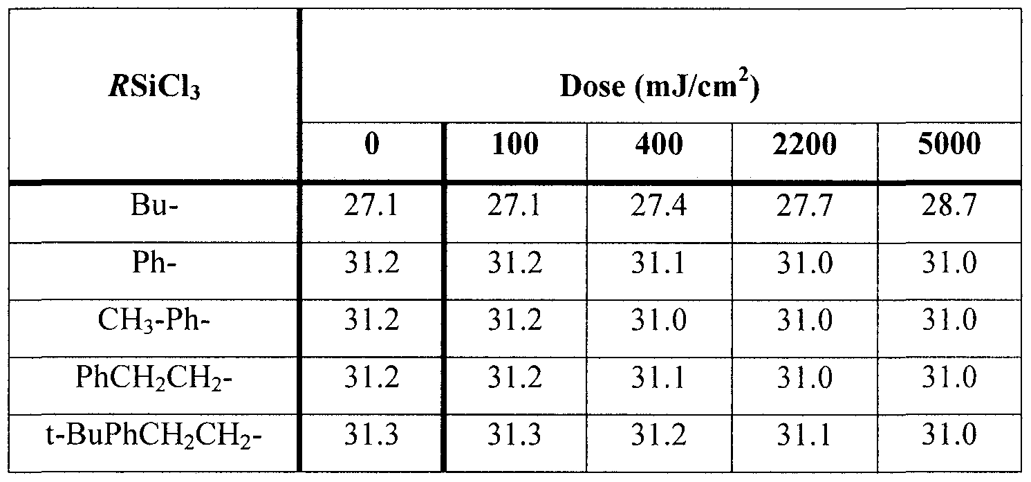
- Wafers coated with the surface modifying agents in Example 1 were exposed to a series of different exposure doses at 193 nm in the manner listed in General Exposure Conditions. Surface energies of each spot were measured as above. The data for representative points are summarized in Tables 5 and 6.
- the example shows the exposure of films of aromatic-based surface modifying agents will change the polar surface energies based on exposure dose.
- the methyl-based surface modifying agents is not absorbing at 193 nm, and thus does not appreciably change polar surface energy upon exposure. All of the surface modifying agents do not appreciably change their dispersive surface energy throughout the exposure dose matrix.
- Example 5 Surface Energy of Diblock Copolymer Components A silicon wafer was vapor primed for 1 minute with hexamethyldisilazide
- HMDS HMDS
- Table 7 Polar and dispersive surface energies of various polymer films.
- the example shows the surface energies of the two components of the diblock copolymers under investigation. These measurements also confirm that there is sufficient polar surface energy difference in order to direct their assembly on a patterned surface. In a random blend of the two components, the surface energy is closer to polymethyl metharylate then polystyrene.
- Wafer A shows a typical surface energy changes for "BuSiCl 3 modified surfaces exposed with 157-nm.
- Re-immersion of an exposed wafer into a toluene solution of "BuSiCl 3 to give Wafer B essentially resets the polar surface energy at each initial dose as if no exposure induced change occurred. No change is observed in dispersive surface energy.
- Exposure of the re-modified wafer at 157-nm to a second series of different exposure doses results in a near duplication of surface energies observed with Wafer A.
- D-G Four silicon wafers (D-G) were cleaned by immersion in CD26 for 10 minutes, rinsed with deionized water and blown dry under a stream of nitrogen. Cleaned wafers D-F were immediately placed into a 10% (v/v) solution Of 11 BuSiCl 3 in toluene for 10 minutes. Wafers were then rinsed with toluene and blown dry under a stream of nitrogen. Wafer G was immersed in a 10% (v/v) solution Of CF 3 CH 2 CH 2 SiCl 3 in toluene for 10 minutes. The wafer was then rinsed with toluene and blown dry under a stream of nitrogen.
- Wafers (D-G) modified with "BuSiCl 3 were exposed at 157-nm to a series of different exposure doses as described in General Exposure Conditions. Wafer D was set aside for surface energy measurements. Wafers E and F were then re- immersed in a solution Of CF 3 CH 2 CH 2 SiCl 3 in toluene for 10 minutes as described in the first step and Wafer E was set aside for surface energy measurements. Wafer F was re- exposed to a second series of 157-nm of different exposure doses as described in General Exposure Conditions and the surface energies measured. Control Wafer G was exposed at 157-nm to a series of different exposure doses as described in the General Exposure Conditions. The data for each wafer is summarized in Table 9.
- Wafer D shows a typical surface energy changes for "BuSiCl 3 modified surfaces exposed with 157-nm.
- Wafer E shows that at low 157-nm exposure doses the surface energy is similar to that of Wafer D as little of the initial surface modifying agent is removed and replaced by the second surface modifying agent. At higher exposure doses the surface energy is similar to that of a surface treated with CF 3 CH 2 CH 2 SiCl 3 as much of the initial surface modifying agent is removed and replaced by the second surface modifying agent.
- Wafer F shows that at low 157-nm exposure doses the surface energy is similar to that of Wafer D as little of the initial surface modifying agent is removed and replaced by the second surface modifying agent. At higher exposure doses the surface energy is similar to that of Wafer G where the second surface modifying agent that initial replaced the first surface modifying agent is now partially removed.
- Wafer G shows the surface energy of surfaces that have treated only with the F 3 CH 2 CH 2 SiCl 3 surface modifying agents and then exposed. This experiment shows that the surface energy can changed be by employing two surface modifying agents and either one or two exposures.
- SAM Sequential Self Assembling Monolayer
- Wafer H Two silicon wafers (H-I) were cleaned by immersion in CD26 for 10 minutes, rinsed with deionized water and blown dry under a stream of nitrogen. Wafer H was immediately placed into a 10% (v/v) solution of "BuSiCl 3 in toluene for 10 minutes. The wafer was then rinsed with toluene and blown dry under a stream of nitrogen. Control Wafer I was immersed in a 10% (v/v) solution Of CF 3 CH 2 CH 2 SiCl 3 in toluene for 10 minutes. The wafer was then rinsed with toluene and blown dry under a stream of nitrogen.
- Wafer H was exposed to a 6x6 matrix of 200 mJ/cm 2 using a 157-nm laser as described as described in General Exposure Conditions. Wafer H was then re-immersed in a solution Of CF 3 CH 2 CH 2 SiCl 3 in toluene for 10 minutes and then the wafer was rinsed with toluene and blown dry under a stream of nitrogen. Both wafers were exposed at 157-nm to a series of different exposure doses as described in General Exposure Conditions and the surface energies measured. The data are summarized in Table 10.
- a silicon wafer was cleaned by immersion in CD26 for 10 minutes, rinsed with deionized water and blown dry under a stream of nitrogen.
- the cleaned wafer was immediately placed into a 10% (v/v) solution Of 1 BuSiCl 3 in toluene for 10 minutes for the SAM film on the silicon surface.
- the wafer was then rinsed with toluene and blown dry under a stream of nitrogen.
- the surface modified wafer was patterned with the 157- nm interference laser system as described above. Polymer films were spun from a 2% (w/w) solution of a Polymer A in toluene at
- the polymer film thickness was determined to be 93 nm.
- the polymer film was annealed at 240 0 C in a vacuum oven for 16 hours. After annealing, it was found that exposing wafer number 9 with an exposure dose of 37 - 47 mJ/cm 2 with the 157-nm interference laser provided enough surface energy differentiation to drive the block copolymer film alignment.
- Example 10 Directed Self-Assembly of P(S-b-MMA) by Hot Plate Annealing on Patterned Surface
- a silicon wafer was cleaned by immersion in CD26 for 10 minutes, rinsed with deionized water and blown dry under a stream of nitrogen.
- the cleaned wafer was immediately placed into a 10% (v/v) solution Of 1 BuSiCl 3 in toluene for 10 minutes.
- the wafer was then rinsed with toluene and blown dry under a stream of nitrogen.
- the surface modified wafer was patterned with the 157-nm interference laser system as described above.
- Polymer films were spun from a 0.9% (w/w) solution of Polymer A in toluene at 2600 rpm for 60 seconds, and then baked for 60 seconds at 130 0 C on a hot plate as described above.
- the polymer film thickness was determined to be 46 nm.
- the polymer film was annealed at 240 0 C on a hot plate in a nitrogen-filled glove box for either 1 or 2 hours.
- the 157-nm interference exposure doses that resulted in aligned polymer films after annealing for each blend can be found in Table 1 1.
- Table 11 Hot plate annealing times of Polymer A and exposure doses which show aligned block copolymer films.
- Example 1 1 - Directed Self-Assembly of P(S-b-MMA) by Hot Plate Annealing on Patterned Surface
- a silicon wafer was cleaned by immersion in CD26 for 10 minutes, rinsed with deionized water and blown dry under a stream of nitrogen.
- the cleaned wafer was immediately placed into a 10% (v/v) solution Of 11 BuSiCl 3 in toluene for 10 minutes.
- the wafer was then rinsed with toluene and blown dry under a stream of nitrogen.
- the surface modified wafer was stored for 4 days at room temperature in air and then patterned with the 157-nm interference laser system as described above.
- Polymer films were spun from a 0.9% (w/w) solution of Polymer A in toluene at 2600 rpm for 60 seconds, and then baked for 60 seconds at 130 0 C on a hot plate as described above.
- the polymer film thickness was determined to be 46 nm.
- the polymer film was annealed at 240 0 C on a hot plate in a nitrogen-filled glove box for either 1 or 2 hours.
- the 157-nm interference exposure doses that resulted in aligned polymer films after annealing for each blend can be found in Table 12.
- Polymer films were spun from a 0.9% (w/w) solution of blended Polymer A/Polymer B block copolymer in toluene at 2600 rpm for 60 seconds, and then baked for 60 seconds at 130 0 C on a hot plate as described above.
- the polymer film thickness was determined to be 46 nm.
- the polymer films were annealed at 240 0 C on a hot plate in a nitrogen-filled glove box for 2 hours.
- the 157-nm interference exposure doses that resulted in aligned polymer films after annealing for each blend can be found in Table 13.
- Example 13 Directed Self-Assembly of a 70:30 Polymer A : Polymer B P(S-b-MMA) Blend by Hot Plate Annealinfi on Patterned SAM Formed from Different RSiCU Concentrations in Toluene.
- the polymer film thickness was determined to be 46 nm.
- the polymer film was annealed at 240 0 C on a hot plate in a nitrogen-filled glove box for 2 hours.
- the 157-nm interference exposure doses that resulted in aligned polymer films after annealing for each blend can be found in Table 14.
- Example 14 Directed Self-Assembly of a 90:10 Polymer A : Polymer B P(S-b-MMA) Blend by Hot Plate Annealing on Patterned SAM at Different Hot Plate Times.
- Polymer films were spun from a 0.9% (w/w) solution of a 90: 10 blend block copolymers A:B in toluene at 2600 rpm for 60 seconds, and then baked for 60 seconds at 130 0 C on a hot plate as described above.
- the polymer film thickness was determined to be 46 nm.
- the polymer film was annealed at 260 0 C on a hot plate in a nitrogen -filled glove box for 0.5, 1 or 2 hours.
- the 157-nm interference exposure doses that resulted in aligned polymer films after annealing for each blend can be found in Table 15.
- a silicon wafer was cleaned by immersion in CD26 for 10 minutes, rinsed with deionized water and blown dry under a stream of nitrogen. The cleaned wafer was immediately placed into a 10% (v/v) solution Of 11 BuSiCl 3 in toluene for 10 minutes.
- the wafer was then rinsed with toluene and blown dry under a stream of nitrogen.
- the surface modified wafer was stored for 2 days at room temperature in air and then patterned with the Lawrence Berkeley National Laboratory on a 0.30 NA microfield exposure tool as described above.
- the exposed wafer was stored for an additional day in air prior to further processing.
- Polymer films were spun from a 0.9% (w/w) solution of Polymer A in toluene at 2600 rpm for 60 seconds, and then baked for 60 seconds at 130 0 C on a hot plate as described above.
- the polymer film thickness was determined to be 45 nm.
- the polymer film was annealed at 260 0 C on a hot plate in a nitrogen-filled glove box for 2 hours. After annealing, it was found that exposing wafer number 15 with an exposure dose of 300 - 400 mJ/cm 2 with the EUV radiation with a mask having 45-nm dense features provided enough surface energy differentiation to drive the block copolymer film alignment.
- Example 16 Partial Polymer Removal and Subsequent Image Transfer
- PMMA block removal was accomplished photochemical Iy either with a 193-nm laser with a 500 mJ/cm 2 exposure dose or a 157-nm laser with a 31 mJ/cm 2 exposure dose.
- the block copolymer was then immersed in a 1 : 1 methyl isobutyl ketone: isopropanol developer for 60 seconds, rinsed with 1 :1 methyl isobutyl ketone: isopropanol, and air dried.
- SEM analysis showed complete removal of the PMMA block occurred with either 193-nm or 157-nm exposure and that the styrene block remained as 45-nm lines with a 91-nm pitch that were 45-nm high.
- the wafer containing only the styrene block as 45-nm lines was placed into a
- PMMA block removal was accomplished by reactive ion etching using an oxygen etch for 1 minute at 10 mTorr (15 seem flow rate) with 100 V bias in a Perkin Elmer Reactive Ion Etcher. SEM analysis showed complete removal of the PMMA block and that the styrene block remained as 45-nm lines with a 91-nm pitch that were
- the wafer containing only the styrene block as 45-nm lines was placed into a Perkin Elmer Reactive Ion Etcher and the underlying silicon was etched for 1.0 minutes using a 95:5 SF6:O2 mixture at 10 mTorr (15 sscm flow rate) with a 60 V bias. These process conditions gave an anisotropic etch into the silicon and yielded a 45-nm lines with a 91-nm pitch grating pattern into silicon that was 34 nm deep.
- Wafers coated with the surface modifying agents in Example 1 were exposed to a series of different exposure doses at 193 nm in the manner listed in General Exposure
- the example shows the exposure of films of aromatic-based surface modifying agents will change the polar surface energies based on exposure dose.
- the butyl-based surface modifying agents is not absorbing at 193 nm, and thus does not appreciably change polar surface energy upon exposure. All of the surface modifying agents do not appreciably change their dispersive surface energy throughout the exposure dose matrix.
- Example 19 Low Defect Directed Self-Assembly It is important to minimize or eliminate defects from directed self-assembly of diblock copolymers.
- Defects in directed self-assembly are primarily dislocation defects caused by an imperfect alignment of the diblock copolymer to the directing surface. These defect can be lines either bridging, terminating in a bridging of adjacent lines, or a line moving from one row to an adjacent row. Defects of less than 1 per ⁇ m 2 are desired. Examples of low or zero defects are shown in FIG. 4 along with an example of higher defects to illustrate types of dislocation defects. The example shows that this directed self-assembly technique is capable of very low defects.
- Example 20 Directed Self-Assembly of P(S-b-MMA) by Hot Plate Annealing on an Electron Beam Patterned Surface
- a silicon wafer was cleaned by immersion in CD26 for 10 minutes, rinsed with deionized water and blown dry under a stream of nitrogen. The cleaned wafer was immediately placed into a 1% (v/v) solution of n BuSiCl 3 in toluene for 20 minutes. The wafer was then rinsed with toluene, blown dry under a stream of nitrogen, and baked on an hot plate at 120 0 C for 5 minutes. The surface modified wafer was then patterned with the electron beam writer by writing a series of lines of 42.5 nm width with a pitch of 85 nm, followed by UV-ozone treatment for any one of 40, 45, or 50 seconds.
- Polymer films were spun from a 0.9% (w/w) solution of Polymer A in toluene at 2600 rpm for 60 seconds, and then baked for 60 seconds at 130 0 C on a hot plate as described above.
- the polymer film thickness was determined to be 45 nm.
- the polymer film was annealed at 260 0 C on a hot plate in a nitrogen-filled glove box for 2 hours.
- the electron beam exposure doses that resulted in aligned polymer films after annealing can be found in Table 18.
- a silicon wafer was cleaned by immersion in CD26 for 10 minutes, rinsed with deionized water and blown dry under a stream of nitrogen.
- the cleaned wafer was immediately placed into a 1% (v/v) solution of "BuSiCl 3 in toluene for 20 minutes.
- the wafer was then rinsed with toluene, blown dry under a stream of nitrogen, and baked on a hot plate at 120 0 C for 5 minutes.
- the surface modified wafer was then patterned with the electron beam writer by writing a series of lines of 22.5 nm width with a pitch of 45 nm followed by to UV-ozone treatment for either 40 or 45 seconds.
- Polymer films were spun from a 1.9% (w/w) solution of Polymer C in toluene at 1350 rpm for 60 seconds, and then baked for 60 seconds at 130 0 C on a hot plate as described above.
- the polymer film thickness was determined to be 45 nm.
- the polymer film was annealed at 220 0 C on a hot plate in a nitrogen-filled glove box for 2 hours.
- the electron beam exposure doses that resulted in aligned polymer films after annealing can be found in Table 19.
- Example 22 Directed Self-Assembly of P(S-b-MMA) by Hot Plate Annealing on an Electron Beam Patterned Surface
- a silicon wafer was cleaned by immersion in CD26 for 10 minutes, rinsed with deionized water and blown dry under a stream of nitrogen. The cleaned wafer was immediately placed into a 1% (v/v) solution Of 11 BuSiCl 3 in toluene for 20 minutes. The wafer was then rinsed with toluene, blown dry under a stream of nitrogen, and baked on a hot plate at 120 0 C for 5 minutes. The surface modified wafer was then patterned with the electron beam writer by writing a series of lines of 22.5 nm width with a pitch of 45 nm followed by to UV-ozone treatment for 45 seconds.
- Polymer films were spun from a 1.9% (w/w) solution of Polymer C in toluene at 1350 rpm for 60 seconds, and then baked for 60 seconds at 13O 0 C on a hot plate as described above.
- the polymer film thickness was determined to be 45 nm.
- the polymer film was annealed at 24O 0 C on a hot plate in a nitrogen-filled glove box for 2 hours. Aligned polymer films after annealing were observed for electron beam exposure doses between 2250 and 2500 ⁇ C/cm 2 .
- a silicon wafer was cleaned by immersion in CD26 for 10 minutes, rinsed with deionized water and blown dry under a stream of nitrogen.
- the cleaned wafer was immediately placed into a 1% (v/v) solution of "BuSiCb in toluene for 20 minutes.
- the wafer was then rinsed with toluene, blown dry under a stream of nitrogen, and baked on a hot plate at 12O 0 C for 5 minutes.
- the surface modified wafer was then patterned with the electron beam writer by writing a series of lines of 22.5 nm width with a pitch of either 45 or 47.5 nm followed by to UV-ozone treatment for 45 seconds.
- Polymer films were spun from a 1.9% (w/w) solution of Polymer C in toluene at
- a silicon wafer was cleaned by immersion in CD26 for 10 minutes, rinsed with deionized water and blown dry under a stream of nitrogen. The cleaned wafer was immediately placed into a 1% (v/v) solution Of 1 BuSiCl 3 in toluene for 20 minutes. The wafer was then rinsed with toluene, blown dry under a stream of nitrogen, and baked on a hot plate at 12O 0 C for 5 minutes. The surface modified wafer was then patterned with the electron beam writer by writing a series of lines of 22.5 nm width with a pitch of 47.5 nm followed by to UV-ozone treatment for 45 seconds. Polymer films were spun from a 1.9% (w/w) solution of Polymer C in toluene at
- Example 25 Directed Self-Assembly of P(S-b-MMA) by Hot Plate Annealing on an Electron Beam Patterned Surface
- a silicon wafer was cleaned by immersion in CD26 for 10 minutes, rinsed with deionized water and blown dry under a stream of nitrogen.
- the cleaned wafer was immediately placed into a 1% (v/v) solution of "BuSiCl 3 in toluene for 20 minutes.
- the wafer was then rinsed with toluene, blown dry under a stream of nitrogen, and baked on a hot plate at 120 0 C for 5 minutes.
- the surface modified wafer was then patterned with the electron beam writer by writing a series of lines of 22.5 nm width with a pitch of 95 nm followed by to UV-ozone treatment for 45 seconds.
- Polymer films were spun from a 1.9% (w/w) solution of Polymer C in toluene at
- the polymer film thickness was determined to be 25 nm.
- the polymer film was annealed at 26O 0 C on a hot plate in a nitrogen-filled glove box for 2 hours. Aligned polymer films after annealing were observed for an electron beam exposure dose of 5788 ⁇ C/cm 2 . This result shows that diblock polymer assembly occurs without the need to pattern every line. Instead patterning a fraction of desired lines is sufficient to guide assembly of a desired structure.
Landscapes
- Physics & Mathematics (AREA)
- Engineering & Computer Science (AREA)
- Chemical & Material Sciences (AREA)
- General Physics & Mathematics (AREA)
- Manufacturing & Machinery (AREA)
- Analytical Chemistry (AREA)
- Microelectronics & Electronic Packaging (AREA)
- Nanotechnology (AREA)
- Spectroscopy & Molecular Physics (AREA)
- Chemical Kinetics & Catalysis (AREA)
- Inorganic Chemistry (AREA)
- Organic Chemistry (AREA)
- Exposure And Positioning Against Photoresist Photosensitive Materials (AREA)
- Photosensitive Polymer And Photoresist Processing (AREA)
Abstract
Description




Claims


Applications Claiming Priority (2)
| Application Number | Priority Date | Filing Date | Title |
|---|---|---|---|
| US15371509P | 2009-02-19 | 2009-02-19 | |
| US61/153,715 | 2009-02-19 |
Publications (2)
| Publication Number | Publication Date |
|---|---|
| WO2010141115A2 true WO2010141115A2 (en) | 2010-12-09 |
| WO2010141115A3 WO2010141115A3 (en) | 2011-03-24 |
Family
ID=43298374
Family Applications (1)
| Application Number | Title | Priority Date | Filing Date |
|---|---|---|---|
| PCT/US2010/024412 Ceased WO2010141115A2 (en) | 2009-02-19 | 2010-02-17 | Directed material assembly |
Country Status (2)
| Country | Link |
|---|---|
| US (1) | US8551566B2 (en) |
| WO (1) | WO2010141115A2 (en) |
Cited By (1)
| Publication number | Priority date | Publication date | Assignee | Title |
|---|---|---|---|---|
| FR3032714A1 (en) * | 2015-02-18 | 2016-08-19 | Arkema France | METHOD FOR REDUCING THE TIME OF ASSEMBLY OF ORDERED BLOCK COPOLYMER FILMS |
Families Citing this family (15)
| Publication number | Priority date | Publication date | Assignee | Title |
|---|---|---|---|---|
| US8574950B2 (en) * | 2009-10-30 | 2013-11-05 | International Business Machines Corporation | Electrically contactable grids manufacture |
| JP5542766B2 (en) * | 2011-09-26 | 2014-07-09 | 株式会社東芝 | Pattern formation method |
| JP5694109B2 (en) | 2011-09-26 | 2015-04-01 | 株式会社東芝 | Pattern formation method |
| US9235125B2 (en) | 2012-03-02 | 2016-01-12 | Asml Netherlands B.V. | Methods of providing patterned chemical epitaxy templates for self-assemblable block copolymers for use in device lithography |
| US9159558B2 (en) | 2013-03-15 | 2015-10-13 | International Business Machines Corporation | Methods of reducing defects in directed self-assembled structures |
| FR3008986B1 (en) * | 2013-07-25 | 2016-12-30 | Arkema France | METHOD OF CONTROLLING THE PERIOD CHARACTERIZING THE MORPHOLOGY OBTAINED FROM A MIXTURE OF BLOCK COPOLYMER AND (CO) POLYMER FROM ONE OF THE BLOCKS |
| KR102235041B1 (en) | 2014-02-12 | 2021-04-02 | 삼성전자주식회사 | Method of manufacturing semiconductor device |
| JP6262044B2 (en) * | 2014-03-20 | 2018-01-17 | 株式会社東芝 | Pattern forming method and semiconductor device manufacturing method |
| JP6456238B2 (en) * | 2015-05-14 | 2019-01-23 | ルネサスエレクトロニクス株式会社 | Manufacturing method of semiconductor device |
| US20170092533A1 (en) * | 2015-09-29 | 2017-03-30 | Applied Materials, Inc. | Selective silicon dioxide deposition using phosphonic acid self assembled monolayers as nucleation inhibitor |
| TWI730990B (en) | 2015-10-04 | 2021-06-21 | 美商應用材料股份有限公司 | Methods for depositing dielectric barrier layers and aluminum containing etch stop layers |
| US10141183B2 (en) * | 2016-01-28 | 2018-11-27 | Tokyo Electron Limited | Methods of spin-on deposition of metal oxides |
| EP3523823B1 (en) * | 2016-10-04 | 2022-03-23 | Brewer Science Inc. | Chemically patterned guide layers for use in chemoepitaxy directing of block co-polymers |
| US10074559B1 (en) | 2017-03-07 | 2018-09-11 | Applied Materials, Inc. | Selective poreseal deposition prevention and residue removal using SAM |
| US20190164890A1 (en) * | 2017-11-30 | 2019-05-30 | Intel Corporation | Pitch-divided interconnects for advanced integrated circuit structure fabrication |
Family Cites Families (6)
| Publication number | Priority date | Publication date | Assignee | Title |
|---|---|---|---|---|
| US6746825B2 (en) | 2001-10-05 | 2004-06-08 | Wisconsin Alumni Research Foundation | Guided self-assembly of block copolymer films on interferometrically nanopatterned substrates |
| WO2004001756A1 (en) | 2002-06-21 | 2003-12-31 | Seagate Technology Llc | Disc drive component with self-assembled monolayers______ |
| US6925953B1 (en) * | 2004-01-23 | 2005-08-09 | Carmelo Batista | Levitation and stabilizing hull system |
| WO2006112887A2 (en) | 2004-11-22 | 2006-10-26 | Wisconsin Alumni Research Foundation | Methods and compositions for forming aperiodic patterned copolymer films |
| WO2008153615A2 (en) * | 2007-03-07 | 2008-12-18 | Ada Technologies, Inc. | Preparing carbohydrate microarrays and conjugated nanoparticles |
| KR101291223B1 (en) | 2007-08-09 | 2013-07-31 | 한국과학기술원 | Method of forming fine pattern using block copolymer |
-
2010
- 2010-02-17 WO PCT/US2010/024412 patent/WO2010141115A2/en not_active Ceased
- 2010-02-17 US US12/707,129 patent/US8551566B2/en not_active Expired - Fee Related
Cited By (1)
| Publication number | Priority date | Publication date | Assignee | Title |
|---|---|---|---|---|
| FR3032714A1 (en) * | 2015-02-18 | 2016-08-19 | Arkema France | METHOD FOR REDUCING THE TIME OF ASSEMBLY OF ORDERED BLOCK COPOLYMER FILMS |
Also Published As
| Publication number | Publication date |
|---|---|
| US8551566B2 (en) | 2013-10-08 |
| WO2010141115A3 (en) | 2011-03-24 |
| US20110039061A1 (en) | 2011-02-17 |
Similar Documents
| Publication | Publication Date | Title |
|---|---|---|
| US8551566B2 (en) | Directed material assembly | |
| US9005756B2 (en) | Block copolymer nanostructure formed on surface pattern with shape different from nanostructure of the block copolymer and method for preparation thereof | |
| TWI464544B (en) | Pattern formation method | |
| Son et al. | Assembly of sub-10-nm block copolymer patterns with mixed morphology and period using electron irradiation and solvent annealing | |
| US8133534B2 (en) | Methods and compositions for forming patterns with isolated or discrete features using block copolymer materials | |
| JP5318217B2 (en) | Pattern formation method | |
| WO2008047817A1 (en) | Pattern forming method | |
| NL2007940A (en) | Methods for providing patterned orientation templates for self-assemblable polymers for use in device lithography. | |
| JP6810782B2 (en) | Silicon-containing block copolymers for inducible self-assembly application | |
| JP2013073974A (en) | Method of forming pattern | |
| Singh et al. | Performance evaluation of nonchemically amplified negative tone photoresists for e-beam and EUV lithography | |
| CN100418011C (en) | Method for manufacturing microstructure | |
| JP2023061994A (en) | Novel compositions and methods for self-assembly of block copolymers | |
| Handte et al. | Manufacturing of nanostructures with high aspect ratios using soft UV-nanoimprint lithography with bi-and trilayer resist systems | |
| KR20140001760A (en) | Method of forming fine pattern, and developing solution | |
| US6673525B1 (en) | Thin layer imaging process for microlithography using radiation at strongly attenuated wavelengths | |
| Takei | UV nanoimprint lithography of 70 nm half pitch line pattern using plant-based resist material with lactulose derivative derived from biomass and medicinal drugs | |
| KR20140090018A (en) | Methods of patterning block copolymer layers and patterned structures | |
| US20240182701A1 (en) | Resin composition for forming phase-separated structure, method of producing structure containing phase-separated structure, and block copolymer | |
| WO2010005892A1 (en) | Resist composition and lithographic process using said composition | |
| Liu et al. | Improved block copolymer domain dispersity on chemical patterns via homopolymer-blending and molecular transfer printing | |
| US20070065756A1 (en) | High sensitivity electron beam resist processing | |
| Kingsborough et al. | Lithographically directed materials assembly | |
| Chen et al. | Nanofabrication of Silicon Gratings Enabled by Vapor-Phase, Highly Uniform Self-Assembled Monolayer Resists | |
| WO2014191163A1 (en) | Method of simulating formation of lithography features by self-assembly of block copolymers |
Legal Events
| Date | Code | Title | Description |
|---|---|---|---|
| 121 | Ep: the epo has been informed by wipo that ep was designated in this application |
Ref document number: 10783728 Country of ref document: EP Kind code of ref document: A2 |
|
| NENP | Non-entry into the national phase |
Ref country code: DE |
|
| 122 | Ep: pct application non-entry in european phase |
Ref document number: 10783728 Country of ref document: EP Kind code of ref document: A2 |
|
| WWE | Wipo information: entry into national phase |
Ref document number: 1201004029 Country of ref document: TH |
|
| WWE | Wipo information: entry into national phase |
Ref document number: 1201004029 Country of ref document: TH |