WO2010068055A2 - Planar gate-controlled element and method for fabricating the same - Google Patents
Planar gate-controlled element and method for fabricating the same Download PDFInfo
- Publication number
- WO2010068055A2 WO2010068055A2 PCT/KR2009/007414 KR2009007414W WO2010068055A2 WO 2010068055 A2 WO2010068055 A2 WO 2010068055A2 KR 2009007414 W KR2009007414 W KR 2009007414W WO 2010068055 A2 WO2010068055 A2 WO 2010068055A2
- Authority
- WO
- WIPO (PCT)
- Prior art keywords
- gate
- source
- drain
- electrode
- electrodes
- Prior art date
- Legal status (The legal status is an assumption and is not a legal conclusion. Google has not performed a legal analysis and makes no representation as to the accuracy of the status listed.)
- Ceased
Links
Images




Classifications
-
- H—ELECTRICITY
- H10—SEMICONDUCTOR DEVICES; ELECTRIC SOLID-STATE DEVICES NOT OTHERWISE PROVIDED FOR
- H10K—ORGANIC ELECTRIC SOLID-STATE DEVICES
- H10K10/00—Organic devices specially adapted for rectifying, amplifying, oscillating or switching; Organic capacitors or resistors having potential barriers
- H10K10/40—Organic transistors
- H10K10/46—Field-effect transistors, e.g. organic thin-film transistors [OTFT]
- H10K10/462—Insulated gate field-effect transistors [IGFETs]
- H10K10/481—Insulated gate field-effect transistors [IGFETs] characterised by the gate conductors
-
- H—ELECTRICITY
- H10—SEMICONDUCTOR DEVICES; ELECTRIC SOLID-STATE DEVICES NOT OTHERWISE PROVIDED FOR
- H10K—ORGANIC ELECTRIC SOLID-STATE DEVICES
- H10K10/00—Organic devices specially adapted for rectifying, amplifying, oscillating or switching; Organic capacitors or resistors having potential barriers
- H10K10/40—Organic transistors
- H10K10/46—Field-effect transistors, e.g. organic thin-film transistors [OTFT]
-
- H—ELECTRICITY
- H10—SEMICONDUCTOR DEVICES; ELECTRIC SOLID-STATE DEVICES NOT OTHERWISE PROVIDED FOR
- H10K—ORGANIC ELECTRIC SOLID-STATE DEVICES
- H10K85/00—Organic materials used in the body or electrodes of devices covered by this subclass
- H10K85/10—Organic polymers or oligomers
- H10K85/111—Organic polymers or oligomers comprising aromatic, heteroaromatic, or aryl chains, e.g. polyaniline, polyphenylene or polyphenylene vinylene
- H10K85/113—Heteroaromatic compounds comprising sulfur or selene, e.g. polythiophene
-
- H—ELECTRICITY
- H10—SEMICONDUCTOR DEVICES; ELECTRIC SOLID-STATE DEVICES NOT OTHERWISE PROVIDED FOR
- H10K—ORGANIC ELECTRIC SOLID-STATE DEVICES
- H10K2102/00—Constructional details relating to the organic devices covered by this subclass
- H10K2102/10—Transparent electrodes, e.g. using graphene
- H10K2102/101—Transparent electrodes, e.g. using graphene comprising transparent conductive oxides [TCO]
- H10K2102/103—Transparent electrodes, e.g. using graphene comprising transparent conductive oxides [TCO] comprising indium oxides, e.g. ITO
Definitions
- the present invention relates to a gate electrode-controlled semiconductor element that is applicable to a semiconductor device including an organic transistor, a biosensor, and a biochip, as well as to a biodevice.
- An organic transistor is a transistor that has an active layer made of organic matter. Like silicon-based transistors, the organic transistor can control the amount of current flowing between a source electrode and a drain electrode according to the amount of voltage or current applied to a gate electrode.
- a biosensor is a semiconductor element that has been proposed to detect or identify an analyte (i.e., a type of chemical substance) based on the substrate specificity of an enzyme or on an antigen-antibody reaction in which biological substances strongly react with a specific substance.
- Biosensors are used in medical fields to detect the amount of urea in the urine; in the food industry to detect alcohol produced during the manufacture of foods, to measure organic acids, and to evaluate the freshness of fish meat; and in environmental fields to detect environmental pollutants or the like in wastewater or rivers.
- the biosensor fixes organic matter such as Deoxyribonucleic Acids (DNAs), proteins, enzymes, antigens, antibodies, hormones, microorganisms, cells, and the like to an electrode so that a computer can read a reaction to a specific chemical substance.
- DNAs Deoxyribonucleic Acids
- proteins proteins
- enzymes enzymes
- antigens antibodies
- hormones hormones
- microorganisms cells
- the like fixes organic matter such as Deoxyribonucleic Acids (DNAs), proteins, enzymes, antigens, antibodies, hormones, microorganisms, cells, and the like to an electrode so that a computer can read a reaction to a specific chemical substance.
- Both the organic transistor and biosensor are semiconductor elements that are controlled by a gate electrode.
- a gate electrode In order to fabricate such an element, it is necessary to carry out procedures of coating an active layer made of organic matter or a biological substance over a substrate and then depositing an electrode-forming metal over the active layer.
- a procedure of forming a metal electrode using thermal deposition, sputtering, electron beams, or the like has to be performed two or more times.
- the metal deposition limits the use of organic matter or biological substances such as protein, which are vulnerable to heat.
- the present invention has been devised to solve the foregoing problems with a semiconductor element that includes an active layer made of organic matter or a biological substance, such problems being related to the formation of metal electrodes after the formation of the active layer.
- Various aspects of the present invention provide a planar gate-controlled element and a method for fabricating the same, in which a source electrode, a drain electrode, and a gate electrode are additionally formed in the same plane.
- the planar gate-controlled element may include a substrate; one or more gate electrodes formed over the substrate, wherein a control voltage or a control current is applied to the gate electrodes; and source and drain electrodes formed in the same plane as the gate electrode over the substrate, wherein signals input into and output from the source and drain electrodes are controlled according to the control voltage or current applied to the gate electrodes.
- the planar gate-controlled element may further include an active layer formed over the gate, source, and drain electrodes.
- the substrate may be made of one selected from among glass, plastic, and metal.
- the source and drain electrodes may be formed parallel to each other at a predetermined interval, and the gate electrodes may include a channel control region extending therefrom, which is positioned between the source electrode and the drain electrode, thereby adjusting a channel interval between the source and drain electrodes.
- the gate electrodes may be two gate electrodes formed on both sides of the source electrode and the drain electrodes, and the source, drain, and two gate electrodes may be arranged in such a manner that the two gate electrodes oppose the source and drain electrodes about the X-shaped diagonals.
- the method for fabricating a planar gate-controlled element may include the following steps of forming an electrode layer over a substrate; coating a photoresist over the electrode layer; selectively exposing a portion of the photoresist to be removed using a mask, which is patterned to form a source electrode, a drain electrode, and one or more gate electrodes; exposing a portion of the electrode layer by removing the exposed portion of the photoresist using a developer solution; forming the source electrode, the drain electrode, and the gate electrodes by removing the exposed portion of the electrode layer using thin-film etching; and stripping the remaining portion of the photoresist from the electrode.
- the method for fabricating a planar gate-controlled element may further include the step of forming an active layer over the substrate and the source, drain, and gate electrodes.
- the substrate may be made of one selected from among glass, plastic, and metal.
- the source electrode and the gate electrode may be formed parallel to each other at a predetermined interval, and the gate electrodes may include a channel control region extending therefrom, which is positioned between the source electrode and the drain electrode, thereby adjusting the channel interval between the source and drain electrodes.
- the gate electrodes may be two gate electrodes formed on both sides of the source electrode and the drain electrodes, and the source, drain, and two gate electrodes may be arranged in such a manner that the two gate electrodes oppose the source and drain electrodes about the X-shaped diagonals.
- source and drain electrodes and one or more charge-controlling gate electrodes are formed in advance in the same plane over the substrate, it is possible to fabricate a biosensor or an organic transistor, which has to be controlled by the gate electrodes, in a simple manner merely by forming an active layer over the electrodes. This can consequently exclude the complicated process of depositing metal over the active layer. Furthermore, it is also possible to advantageously form the active layer using organic matter or a biological substance such as protein, which has been difficult to use together with metal deposition since it is vulnerable to heat.
- FIG. 1 is a top plan view showing the structure of a planar gate-controlled element according to one exemplary embodiment of the invention
- FIG. 2 is a photograph of a planar gate-controlled element realized according to the structure shown in FIG. 1;
- FIG. 3 is a top plan view showing the structure of a planar gate-controlled element according to another exemplary embodiment of the invention.
- FIG. 4 is a photograph of a planar gate-controlled element realized according to the structure shown in FIG. 3;
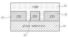
- FIG. 5 is a cross-sectional view showing a first application example of a planar gate-controlled element according to the invention.
- FIG. 6A is a graph showing the variation of current with respect to gate voltage in the element shown in FIG. 5;
- FIG. 6B is a graph showing the variation of current with respect to drain voltage in the element shown in FIG. 5;
- FIG. 7 is a cross-sectional view showing a second application example of a planar gate-controlled element according to the invention.
- FIG. 8A is a graph showing the variation of current with respect to gate voltage in the element shown in FIG. 7;
- FIG. 8B is a graph showing the variation of current with respect to drain voltage in the element shown in FIG. 7.
- FIG. 1 is a top plan view showing the structure of a planar gate-controlled element according to one exemplary embodiment of the invention.
- the planar gate-controlled element of this embodiment includes a source electrode 12, a drain electrode 13, and a gate electrode 14, which are formed in the same plane on a substrate 11.
- the source and drain electrodes 12 and 13 are disposed to oppose each other with a predetermined interval between them.
- the gate electrode 14 includes a channel control region 14a extending therefrom.
- the channel control region 14a is positioned between the source and drain electrodes 12 and 13, thereby adjusting the channel interval between the source and drain electrodes 12 and 13.
- the substrate 11 is made of glass, metal, or plastic.
- the gate, source, and drain electrodes can be made from a conductive oxide, examples of which may include Indium Tin Oxide (ITO), zinc oxide, tin oxide, and the like.
- ITO Indium Tin Oxide
- FIG. 2 is a photograph of an actual planar gate-controlled element, which is realized according to the structure shown in FIG. 1.
- FIG. 3 is a top plan view showing the structure of a planar gate-controlled element according to another exemplary embodiment of the invention.
- the planar gate-controlled element of this embodiment includes a source electrode 32, a drain electrode 33, and two gate electrodes 34 and 35, which are present together in the same plane on a substrate 31.
- the source electrode 32, the drain electrode 33, and the two gate electrodes 34 and 35 are arranged in such a manner that the two gate electrodes 34 and 35 oppose the source and drain electrodes 32 and 33 about the X-shaped diagonals.
- channels can be activated in both directions to the source and drain electrodes 32 and 33 through the two gate electrodes 34 and 35.
- FIG. 4 is a photograph of an actual planar gate-controlled element, which is realized according to the structure shown in FIG. 3.
- the source electrode 12, 32, the drain electrode 13, 33, and one or more gate electrodes 14, 34 and 35 are formed together in the same plane on the substrate 11, 31.
- planar gate-controlled element can be fabricated by a method including the following steps of: forming an electrode layer over a substrate; coating a photoresist over the electrode layer; selectively exposing a portion of the photoresist to be removed using a mask, which is patterned in the form of a source electrode, a drain electrode, and one or more gate electrodes; exposing a portion of the electrode layer by removing the exposed portion of the photoresist using a developer solution; forming the source, drain, and one or more gate electrodes by removing the exposed portion of the electrode layer; and removing the remaining portion of the photoresist from the electrode.
- the method can also include the step of forming an active layer over the source, drain, and one or more gate electrodes.
- FIGS. 5 and 7 show application examples of planar gate-controlled elements according to respective exemplary embodiments of the invention. With reference to FIGS. 5 and 7, the method for fabricating a planar gate-controlled element according to exemplary embodiments of the invention will be described in more detail.
- the element shown in FIG. 5 is fabricated according to the following process.
- an electrode layer is formed with a predetermined thickness over a glass substrate 51.
- the electrode layer is made of, for example, Indium Tin Oxide (ITO).
- ITO Indium Tin Oxide
- the electrode layer is formed by applying the ITO with a predetermined thickness over the glass substrate 51, followed by cleaning and then pre-baking to remove moisture.
- a photoresist (not shown) is applied with a uniform thickness over the electrode layer, followed by soft-baking to remove solvent, and a portion of the photoresist to be removed is exposed through a mask, which is patterned in the form of the source, drain, and gate electrodes as shown in FIGS. 1 and 2.
- the portion of the electrode layer to be removed is exposed by selectively removing the exposed portion of the photoresist using a developer solution.
- hard-baking is performed in order to increase the bonding force of the photoresist, the exposed portion of the electrode layer is removed using etchant, and the remaining portion of the photoresist is removed.
- a source electrode 52, a drain electrode 53, and a gate electrode 54 are formed in the same plane.
- an active layer 55 made of Poly 3-Hexylthiophene (P3HT) is formed by spin-coating P3HT with a predetermined thickness, followed by evaporating solvent at 50 °C for 15 minutes.
- FIGS. 6A and 6B are graphs showing the quantities of variation of current with respect to gate and drain voltages in an element realized as shown in FIG. 5. As shown in FIGS. 6A and 6B, it can be seen that a drain current Ids varies according to a gate voltage Vg applied to the gate electrode 54 or a drain voltage Vds applied to the drain electrode 53. From this, it can be understood that the planar gate-controlled element according to an exemplary embodiment of the invention can be controlled through the gate electrode 54.
- the element shown in FIG. 7 is fabricated by forming source, drain, and gate electrodes 72, 73, and 74 over a glass substrate 71 by the same fabrication process as above, and forming an active layer 75 by coating Horseradish Peroxidase (HP) over the source, drain, and gate electrodes 72, 73, and 74.
- HP Horseradish Peroxidase
- FIGS. 8A and 8B are graphs showing the quantities of variation of current with respect to drain and gate voltages in an element realized as shown in FIG. 7. It can be seen that a drain current Id varies according to the drain voltage Vd or the gate voltage Vg. From this, it can be understood that the planar gate-controlled element can be controlled through the gate electrode 74.
- An aspect of the present invention also provides a field effect transistor by forming an insulating layer over the planar gate-controlled element.
- a conventional organic field effect transistor is fabricated by forming a gate electrode over a substrate, forming an insulating layer over the gate electrode, forming an active layer over the insulating layer, and then forming source and drain electrodes over the active layer.
- the field effect transistor according to an exemplary embodiment of the invention is fabricated by forming all of source, drain, and gate electrodes in the same plane, forming an insulating layer around only the gate electrode, and then forming an active layer over the source, drain, and gate electrodes.
- the field effect transistor can be fabricated by depositing a material intended to function as an insulating layer over the planar gate-controlled element produced by the above-described process, and forming an active layer made of organic matter or a biological substance (e.g. protein and DNA) over the element, over which the insulating layer has been deposited.
- a material intended to function as an insulating layer over the planar gate-controlled element produced by the above-described process, and forming an active layer made of organic matter or a biological substance (e.g. protein and DNA) over the element, over which the insulating layer has been deposited.
- An ITO layer deposited with a uniform thickness over a glass substrate was cleaned, followed by preheating (at about 100°C for about 100 seconds) in order to remove moisture, and then a photosensitizer was applied with a uniform thickness over the ITO-deposited substrate. Heating was performed again at about 100°C for 100 about seconds to remove residual solvent from the photosensitizer. A pattern mask was exposed to light, and the portion of the photosensitizer exposed to light was selectively removed using a developer solution. Afterwards, the substrate was heated at 250 °C for about 2 minutes in order to increase the bonding force of the remaining photosensitizer. A pattern was formed in the ITO layer using an etchant solution, and then the remaining photosensitizer was removed, thereby producing a planar gate-controlled element having the pattern.
- HRP Horseradish Peroxidase
- Vg Gate voltage
- Vds drain voltage
- Ids drain current
- the present invention can be applied to a gate-controlled semiconductor element such as an organic transistor and a biosensor. It is possible to realize the organic transistor and the biosensor by a simple process of forming an active layer over a source electrode, a drain electrode, and one or more gate electrodes. Furthermore, it is also possible to increase the application of organic matter or a biological substance such as protein, which has been difficult to use together with metal deposition in the related art since it is vulnerable to heat.
Landscapes
- Chemical & Material Sciences (AREA)
- Engineering & Computer Science (AREA)
- Materials Engineering (AREA)
- Thin Film Transistor (AREA)
Abstract
A planar gate-controlled element and a method for fabricating the same that can facilitate the fabrication of a semiconductor device, such as an organic transistor or a biosensor, which is controlled by a gate electrode. Since source, drain, and gate electrode are formed in the same plane over a substrate, the organic transistor or biosensor can be realized in a simple manner by a process of forming an active layer over the source, drain, and gate electrodes. In addition, it is also possible to use organic matter or a biological substance that is vulnerable to heat.
Description
The present invention relates to a gate electrode-controlled semiconductor element that is applicable to a semiconductor device including an organic transistor, a biosensor, and a biochip, as well as to a biodevice.
An organic transistor is a transistor that has an active layer made of organic matter. Like silicon-based transistors, the organic transistor can control the amount of current flowing between a source electrode and a drain electrode according to the amount of voltage or current applied to a gate electrode.
A biosensor is a semiconductor element that has been proposed to detect or identify an analyte (i.e., a type of chemical substance) based on the substrate specificity of an enzyme or on an antigen-antibody reaction in which biological substances strongly react with a specific substance. Biosensors are used in medical fields to detect the amount of urea in the urine; in the food industry to detect alcohol produced during the manufacture of foods, to measure organic acids, and to evaluate the freshness of fish meat; and in environmental fields to detect environmental pollutants or the like in wastewater or rivers. The biosensor fixes organic matter such as Deoxyribonucleic Acids (DNAs), proteins, enzymes, antigens, antibodies, hormones, microorganisms, cells, and the like to an electrode so that a computer can read a reaction to a specific chemical substance.
Both the organic transistor and biosensor are semiconductor elements that are controlled by a gate electrode. In order to fabricate such an element, it is necessary to carry out procedures of coating an active layer made of organic matter or a biological substance over a substrate and then depositing an electrode-forming metal over the active layer. In particular, in order to complete the element, a procedure of forming a metal electrode using thermal deposition, sputtering, electron beams, or the like has to be performed two or more times.
However, the metal deposition limits the use of organic matter or biological substances such as protein, which are vulnerable to heat.
The information disclosed in this Background of the Invention section is only for the enhancement of understanding of the background of the invention, and should not be taken as an acknowledgment or any form of suggestion that this information forms a prior art that would be already known to a person skilled in the art.
The present invention has been devised to solve the foregoing problems with a semiconductor element that includes an active layer made of organic matter or a biological substance, such problems being related to the formation of metal electrodes after the formation of the active layer. Various aspects of the present invention provide a planar gate-controlled element and a method for fabricating the same, in which a source electrode, a drain electrode, and a gate electrode are additionally formed in the same plane.
According to an aspect of the present invention, the planar gate-controlled element may include a substrate; one or more gate electrodes formed over the substrate, wherein a control voltage or a control current is applied to the gate electrodes; and source and drain electrodes formed in the same plane as the gate electrode over the substrate, wherein signals input into and output from the source and drain electrodes are controlled according to the control voltage or current applied to the gate electrodes.
The planar gate-controlled element may further include an active layer formed over the gate, source, and drain electrodes.
In the planar gate-controlled element, the substrate may be made of one selected from among glass, plastic, and metal.
In the planar gate-controlled element, the source and drain electrodes may be formed parallel to each other at a predetermined interval, and the gate electrodes may include a channel control region extending therefrom, which is positioned between the source electrode and the drain electrode, thereby adjusting a channel interval between the source and drain electrodes.
In the planar gate-controlled element, the gate electrodes may be two gate electrodes formed on both sides of the source electrode and the drain electrodes, and the source, drain, and two gate electrodes may be arranged in such a manner that the two gate electrodes oppose the source and drain electrodes about the X-shaped diagonals.
In an aspect of the present invention, the method for fabricating a planar gate-controlled element may include the following steps of forming an electrode layer over a substrate; coating a photoresist over the electrode layer; selectively exposing a portion of the photoresist to be removed using a mask, which is patterned to form a source electrode, a drain electrode, and one or more gate electrodes; exposing a portion of the electrode layer by removing the exposed portion of the photoresist using a developer solution; forming the source electrode, the drain electrode, and the gate electrodes by removing the exposed portion of the electrode layer using thin-film etching; and stripping the remaining portion of the photoresist from the electrode.
The method for fabricating a planar gate-controlled element may further include the step of forming an active layer over the substrate and the source, drain, and gate electrodes.
In the method for fabricating a planar gate-controlled element, the substrate may be made of one selected from among glass, plastic, and metal.
In the method for fabricating a planar gate-controlled element, the source electrode and the gate electrode may be formed parallel to each other at a predetermined interval, and the gate electrodes may include a channel control region extending therefrom, which is positioned between the source electrode and the drain electrode, thereby adjusting the channel interval between the source and drain electrodes. Alternatively, the gate electrodes may be two gate electrodes formed on both sides of the source electrode and the drain electrodes, and the source, drain, and two gate electrodes may be arranged in such a manner that the two gate electrodes oppose the source and drain electrodes about the X-shaped diagonals.
According to exemplary embodiments of the present invention as set forth above, since source and drain electrodes and one or more charge-controlling gate electrodes are formed in advance in the same plane over the substrate, it is possible to fabricate a biosensor or an organic transistor, which has to be controlled by the gate electrodes, in a simple manner merely by forming an active layer over the electrodes. This can consequently exclude the complicated process of depositing metal over the active layer. Furthermore, it is also possible to advantageously form the active layer using organic matter or a biological substance such as protein, which has been difficult to use together with metal deposition since it is vulnerable to heat.
The methods and apparatuses of the present invention have other features and advantages which will be apparent from, or are set forth in more detail in, the accompanying drawings, which are incorporated herein, and the following Detailed Description of the Invention, which together serve to explain certain principles of the present invention.
FIG. 1 is a top plan view showing the structure of a planar gate-controlled element according to one exemplary embodiment of the invention;
FIG. 2 is a photograph of a planar gate-controlled element realized according to the structure shown in FIG. 1;
FIG. 3 is a top plan view showing the structure of a planar gate-controlled element according to another exemplary embodiment of the invention;
FIG. 4 is a photograph of a planar gate-controlled element realized according to the structure shown in FIG. 3;
FIG. 5 is a cross-sectional view showing a first application example of a planar gate-controlled element according to the invention;
FIG. 6A is a graph showing the variation of current with respect to gate voltage in the element shown in FIG. 5;
FIG. 6B is a graph showing the variation of current with respect to drain voltage in the element shown in FIG. 5;
FIG. 7 is a cross-sectional view showing a second application example of a planar gate-controlled element according to the invention;
FIG. 8A is a graph showing the variation of current with respect to gate voltage in the element shown in FIG. 7; and
FIG. 8B is a graph showing the variation of current with respect to drain voltage in the element shown in FIG. 7.
Reference will now be made in detail to various exemplary embodiments of the present invention(s), examples of which are illustrated in the accompanying drawings and described below. While the invention(s) will be described in conjunction with exemplary embodiments, it will be understood that the present description is not intended to limit the invention(s) to those exemplary embodiments. On the contrary, the invention(s) is/are intended to cover not only the exemplary embodiments, but also various alternatives, modifications, equivalents and other embodiments that may be included within the spirit and scope of the invention as defined by the appended claims.
In the following description of the present invention, detailed descriptions of known functions and components incorporated herein will be omitted when they may make the subject matter of the present invention unclear.
Throughout this document, reference should be made to the drawings, in which the same reference numerals and signs are used throughout the different drawings to designate the same or similar components.
In addition, throughout this specification and the claims that follow, it will be understood that when an element is referred to as being “connected to” or “coupled to” another element, not only can it be “directly connected or coupled to” the other element; it can also be “indirectly connected or coupled to” the other element via an intervening element. Unless explicitly described to the contrary, the word “comprise” and its variations, such as “comprises” or “comprising” will be understood to imply the inclusion of stated elements but not the exclusion of any other elements.
FIG. 1 is a top plan view showing the structure of a planar gate-controlled element according to one exemplary embodiment of the invention.
Referring to FIG. 1, the planar gate-controlled element of this embodiment includes a source electrode 12, a drain electrode 13, and a gate electrode 14, which are formed in the same plane on a substrate 11. The source and drain electrodes 12 and 13 are disposed to oppose each other with a predetermined interval between them. The gate electrode 14 includes a channel control region 14a extending therefrom. The channel control region 14a is positioned between the source and drain electrodes 12 and 13, thereby adjusting the channel interval between the source and drain electrodes 12 and 13.
The substrate 11 is made of glass, metal, or plastic.
In the planar gate-controlled element having the above-described structure, it is possible to variously modify the shape and size of the gate electrode 14 and the channel control region 14a, and thereby control the channel interval between the source and drain electrodes 12 and 13. In addition, the gate, source, and drain electrodes can be made from a conductive oxide, examples of which may include Indium Tin Oxide (ITO), zinc oxide, tin oxide, and the like.
FIG. 2 is a photograph of an actual planar gate-controlled element, which is realized according to the structure shown in FIG. 1.
Next, FIG. 3 is a top plan view showing the structure of a planar gate-controlled element according to another exemplary embodiment of the invention.
Referring to FIG. 3, the planar gate-controlled element of this embodiment includes a source electrode 32, a drain electrode 33, and two gate electrodes 34 and 35, which are present together in the same plane on a substrate 31. The source electrode 32, the drain electrode 33, and the two gate electrodes 34 and 35 are arranged in such a manner that the two gate electrodes 34 and 35 oppose the source and drain electrodes 32 and 33 about the X-shaped diagonals.
In this case, channels can be activated in both directions to the source and drain electrodes 32 and 33 through the two gate electrodes 34 and 35.
FIG. 4 is a photograph of an actual planar gate-controlled element, which is realized according to the structure shown in FIG. 3.
As described above, in the planar gate-controlled element according to the foregoing exemplary embodiments of the invention, the source electrode 12, 32, the drain electrode 13, 33, and one or more gate electrodes 14, 34 and 35 are formed together in the same plane on the substrate 11, 31. Thus, it is possible to realize an organic transistor or a biosensor in a simple matter merely by performing a process of forming an active layer made of organic matter or a biomaterial over the source electrode 12, the drain electrode 13, and the gate electrode 14, or over the source electrode 32, the drain electrode 33, and the gate electrodes 34 and 35.
Accordingly, it is possible to form an active layer using organic matter or a biological substance such as protein, which has been difficult to use together with the metal deposition in the related art since it is vulnerable to heat. This can consequently increase the usefulness of organic matter and biological substances.
The planar gate-controlled element according to any of the foregoing exemplary embodiments of the invention as illustrated above can be fabricated by a method including the following steps of: forming an electrode layer over a substrate; coating a photoresist over the electrode layer; selectively exposing a portion of the photoresist to be removed using a mask, which is patterned in the form of a source electrode, a drain electrode, and one or more gate electrodes; exposing a portion of the electrode layer by removing the exposed portion of the photoresist using a developer solution; forming the source, drain, and one or more gate electrodes by removing the exposed portion of the electrode layer; and removing the remaining portion of the photoresist from the electrode. In addition, the method can also include the step of forming an active layer over the source, drain, and one or more gate electrodes.
FIGS. 5 and 7 show application examples of planar gate-controlled elements according to respective exemplary embodiments of the invention. With reference to FIGS. 5 and 7, the method for fabricating a planar gate-controlled element according to exemplary embodiments of the invention will be described in more detail.
The element shown in FIG. 5 is fabricated according to the following process. First, an electrode layer is formed with a predetermined thickness over a glass substrate 51. The electrode layer is made of, for example, Indium Tin Oxide (ITO). The electrode layer is formed by applying the ITO with a predetermined thickness over the glass substrate 51, followed by cleaning and then pre-baking to remove moisture.
Afterwards, a photoresist (not shown) is applied with a uniform thickness over the electrode layer, followed by soft-baking to remove solvent, and a portion of the photoresist to be removed is exposed through a mask, which is patterned in the form of the source, drain, and gate electrodes as shown in FIGS. 1 and 2. Next, the portion of the electrode layer to be removed is exposed by selectively removing the exposed portion of the photoresist using a developer solution. Afterwards, hard-baking is performed in order to increase the bonding force of the photoresist, the exposed portion of the electrode layer is removed using etchant, and the remaining portion of the photoresist is removed. Then, as shown in FIG. 5, a source electrode 52, a drain electrode 53, and a gate electrode 54 are formed in the same plane.
Afterwards, an active layer 55 made of Poly 3-Hexylthiophene (P3HT) is formed by spin-coating P3HT with a predetermined thickness, followed by evaporating solvent at 50 ℃ for 15 minutes.
FIGS. 6A and 6B are graphs showing the quantities of variation of current with respect to gate and drain voltages in an element realized as shown in FIG. 5. As shown in FIGS. 6A and 6B, it can be seen that a drain current Ids varies according to a gate voltage Vg applied to the gate electrode 54 or a drain voltage Vds applied to the drain electrode 53. From this, it can be understood that the planar gate-controlled element according to an exemplary embodiment of the invention can be controlled through the gate electrode 54.
Next, the element shown in FIG. 7 is fabricated by forming source, drain, and gate electrodes 72, 73, and 74 over a glass substrate 71 by the same fabrication process as above, and forming an active layer 75 by coating Horseradish Peroxidase (HP) over the source, drain, and gate electrodes 72, 73, and 74.
FIGS. 8A and 8B are graphs showing the quantities of variation of current with respect to drain and gate voltages in an element realized as shown in FIG. 7. It can be seen that a drain current Id varies according to the drain voltage Vd or the gate voltage Vg. From this, it can be understood that the planar gate-controlled element can be controlled through the gate electrode 74.
An aspect of the present invention also provides a field effect transistor by forming an insulating layer over the planar gate-controlled element.
A conventional organic field effect transistor is fabricated by forming a gate electrode over a substrate, forming an insulating layer over the gate electrode, forming an active layer over the insulating layer, and then forming source and drain electrodes over the active layer. However, the field effect transistor according to an exemplary embodiment of the invention is fabricated by forming all of source, drain, and gate electrodes in the same plane, forming an insulating layer around only the gate electrode, and then forming an active layer over the source, drain, and gate electrodes. The advantage is that it can be realized by forming only the insulating layer and the active layer without undergoing complicated processes, unlike conventional approaches.
This is because, when a voltage is applied to the gate electrode, an electric charge is induced between the active layer and the insulating layer due to electric field effect caused by the gate voltage, and the induced electric charge flows between the source and the drain.
The field effect transistor can be fabricated by depositing a material intended to function as an insulating layer over the planar gate-controlled element produced by the above-described process, and forming an active layer made of organic matter or a biological substance (e.g. protein and DNA) over the element, over which the insulating layer has been deposited.
Below, the present invention will be described more fully with reference to Example and Experimental Examples.
However, it should be understood that Example and Experimental Examples below illustrate, but by no means limit, the present invention.
Example 1: Fabrication of Planar Gate-Controlled Element
An ITO layer deposited with a uniform thickness over a glass substrate was cleaned, followed by preheating (at about 100℃ for about 100 seconds) in order to remove moisture, and then a photosensitizer was applied with a uniform thickness over the ITO-deposited substrate. Heating was performed again at about 100℃ for 100 about seconds to remove residual solvent from the photosensitizer. A pattern mask was exposed to light, and the portion of the photosensitizer exposed to light was selectively removed using a developer solution. Afterwards, the substrate was heated at 250 ℃ for about 2 minutes in order to increase the bonding force of the remaining photosensitizer. A pattern was formed in the ITO layer using an etchant solution, and then the remaining photosensitizer was removed, thereby producing a planar gate-controlled element having the pattern.
Experimental Example 1: Measurement of Variation of Current in Planar Gate-Controlled Element on Which Polymer Material is Applied
Experimental Example using a planar gate-controlled element is as follows: Poly 3-Hexylthiophene (P3HT) was spin-coated with a thickness of about 55 nm over the planar gate-controlled element, followed by evaporating solvent at 50 ℃ for about 15 minutes. Gate voltage (Vg), drain voltage (Vds), and drain current (Ids) were measured from the planar gate-controlled element, on which P3HT was deposited, using a measuring instrument (Keithley SCS-4200). The results are reported in FIGS. 6A and 6B as below.
As seen in FIGS. 6A and 6B, it can be appreciated that almost no current flowed when the gate voltage was 0 and the drain voltage increased when the gate voltage increased negatively from zero. It can also be appreciated that the amount of current was limited according to a given amount of drain voltage.
Experimental Example 2: Measurement of Variation of Current in Planar Gate-Controlled Element on Which Polymer Material is Applied
Horseradish Peroxidase (HRP) was coated over a planar gate-controlled element. Gate voltage (Vg), drain voltage (Vds), and drain current (Ids) were measured from the planar gate-controlled element, on which HRP is deposited, using a measuring instrument (Keithley SCS-4200). The results are reported in FIGS. 8A and 8B as below.
As seen in FIGS. 8A and 8B, it can be appreciated that almost no current flowed when the gate voltage was 0 and the drain voltage increased when the gate voltage increased negatively from zero. It can also be appreciated that the amount of current was limited according to a given amount of drain voltage.
While the present invention has been shown and described with reference to certain exemplary embodiments thereof and the accompanying drawings, it will be understood by those skilled in the art that various changes in form and details may be made therein without departing from the spirit and scope of the present invention as defined by the appended claims and their equivalents.
The present invention can be applied to a gate-controlled semiconductor element such as an organic transistor and a biosensor. It is possible to realize the organic transistor and the biosensor by a simple process of forming an active layer over a source electrode, a drain electrode, and one or more gate electrodes. Furthermore, it is also possible to increase the application of organic matter or a biological substance such as protein, which has been difficult to use together with metal deposition in the related art since it is vulnerable to heat.
Claims (12)
- A planar gate-controlled element comprising:a substrate;one or more gate electrodes formed over the substrate, wherein a control voltage or a control current is applied to the gate electrodes; andsource and drain electrodes formed in the same plane as the gate electrode over the substrate, wherein signals input into and output from the source and drain electrodes are controlled according to the control voltage or current applied to the gate electrodes.
- The planar gate-controlled element according to claim 1, further comprising an active layer formed over the gate, source, and drain electrodes.
- The planar gate-controlled element according to claim 1, wherein the substrate is made of one selected from the group consisting of glass, plastic, and metal.
- The planar gate-controlled element according to claim 1, wherein the source and drain electrodes are formed parallel to each other at a predetermined interval.
- The planar gate-controlled element according to claim 1, wherein the gate electrodes include a channel control region extending therefrom, wherein the channel control region is positioned between the source electrode and the drain electrode, thereby adjusting a channel interval between the source and drain electrodes.
- The planar gate-controlled element according to claim 1, wherein the gate electrodes comprise two gate electrodes formed on both sides of the source electrode and the drain electrodes,wherein the source, drain, and two gate electrodes are arranged in such a manner that the two gate electrodes oppose the source and drain electrodes about the X-shaped diagonals.
- A method for fabricating a planar gate-controlled element, comprising:forming an electrode layer over a substrate;coating a photoresist over the electrode layer;selectively exposing a portion of the photoresist to be removed using a mask, which is patterned to form a source electrode, a drain electrode, and one or more gate electrodes;exposing a portion of the electrode layer by removing the exposed portion of the photoresist using a developer solution;forming the source electrode, the drain electrode, and the gate electrodes by removing the exposed portion of the electrode layer using thin-film etching; andstripping a remaining portion of the photoresist from the electrode.
- The method according to claim 7, further comprising forming an active layer over the substrate and the source, drain, and gate electrodes.
- The method according to claim 7, wherein the substrate is made of one selected from the group consisting of glass, plastic, and metal.
- The method according to claim 7, wherein the source electrode and the gate electrode are formed in parallel to each other at a predetermined interval, and the gate electrodes include a channel control region extending therefrom, the channel control region positioned between the source electrode and the drain electrode, thereby adjusting the channel interval between the source and drain electrodes.
- The method according to claim 7, wherein the gate electrodes comprise two gate electrodes formed on both sides of the source electrode and the drain electrodes,wherein the source, drain, and two gate electrodes are arranged in such a manner that the two gate electrodes oppose the source and drain electrodes about the X-shaped diagonals.
- A field effect transistor comprising one or more insulating layers formed over gate electrodes of a planar gate-controlled element as described in any one of the preceding claims 1 to 6.
Applications Claiming Priority (2)
| Application Number | Priority Date | Filing Date | Title |
|---|---|---|---|
| KR10-2008-0125966 | 2008-12-11 | ||
| KR1020080125966A KR101083843B1 (en) | 2008-12-11 | 2008-12-11 | Planar Gate-Controlled Device and manufacturing method thereof |
Publications (2)
| Publication Number | Publication Date |
|---|---|
| WO2010068055A2 true WO2010068055A2 (en) | 2010-06-17 |
| WO2010068055A3 WO2010068055A3 (en) | 2010-09-30 |
Family
ID=42243233
Family Applications (1)
| Application Number | Title | Priority Date | Filing Date |
|---|---|---|---|
| PCT/KR2009/007414 Ceased WO2010068055A2 (en) | 2008-12-11 | 2009-12-11 | Planar gate-controlled element and method for fabricating the same |
Country Status (2)
| Country | Link |
|---|---|
| KR (1) | KR101083843B1 (en) |
| WO (1) | WO2010068055A2 (en) |
Families Citing this family (1)
| Publication number | Priority date | Publication date | Assignee | Title |
|---|---|---|---|---|
| CN113488590B (en) * | 2021-07-05 | 2025-01-10 | 南京大学 | A planar organic rectifier diode structure and manufacturing method thereof |
Family Cites Families (4)
| Publication number | Priority date | Publication date | Assignee | Title |
|---|---|---|---|---|
| JP2936586B2 (en) * | 1989-07-25 | 1999-08-23 | ソニー株式会社 | Method of manufacturing high electron mobility field effect transistor |
| KR100299664B1 (en) * | 1997-10-01 | 2001-10-27 | 오길록 | Secondary electron proximity effect of electron drawing and silicon single electron transistor fabrication method using silicon oxide |
| GB2423634A (en) * | 2005-02-25 | 2006-08-30 | Seiko Epson Corp | A patterning method for manufacturing high resolution structures |
| KR20060001985A (en) * | 2005-12-23 | 2006-01-06 | 황성우 | Manufacturing method of single electron transistor using compound semiconductor |
-
2008
- 2008-12-11 KR KR1020080125966A patent/KR101083843B1/en not_active Expired - Fee Related
-
2009
- 2009-12-11 WO PCT/KR2009/007414 patent/WO2010068055A2/en not_active Ceased
Also Published As
| Publication number | Publication date |
|---|---|
| WO2010068055A3 (en) | 2010-09-30 |
| KR20100067409A (en) | 2010-06-21 |
| KR101083843B1 (en) | 2011-11-15 |
Similar Documents
| Publication | Publication Date | Title |
|---|---|---|
| Liu et al. | Ultrafast, sensitive, and portable detection of COVID-19 IgG using flexible organic electrochemical transistors | |
| Tang et al. | Solution processed low power organic field-effect transistor bio-chemical sensor of high transconductance efficiency | |
| Seshadri et al. | Low-picomolar, label-free procalcitonin analytical detection with an electrolyte-gated organic field-effect transistor based electronic immunosensor | |
| Li et al. | Flexible organic field-effect transistor arrays for wearable neuromorphic device applications | |
| WO2012099446A2 (en) | Transparent ion sensor chip using a field-effect-transistor-type signal converter in which an extended gate electrode is formed, and method for manufacturing the sensor chip | |
| Tixier-Mita et al. | Review on thin-film transistor technology, its applications, and possible new applications to biological cells | |
| Liang et al. | Amplification‐free detection of SARS‐CoV‐2 down to single virus level by portable carbon nanotube biosensors | |
| AU2007227415B2 (en) | Apparatus for microarray binding sensors having biological probe materials using carbon nanotube transistors | |
| JP4775262B2 (en) | Sensor unit, reaction field cell unit and analyzer | |
| TWI702393B (en) | Semiconductor element, its manufacturing method and sensor using the same | |
| Demelas et al. | Charge sensing by organic charge-modulated field effect transistors: Application to the detection of bio-related effects | |
| WO2010056049A2 (en) | Humidity sensor of capacitance type and method of fabricating same | |
| WO2009119971A2 (en) | Method for electrically detecting physiologically active materials and biochip for the same | |
| Zhang et al. | Fabrication of organic electrochemical transistor arrays for biosensing | |
| Wu et al. | Sequentially multiplexed amperometry for electrochemical biosensors | |
| WO2013100264A1 (en) | Biosensor and method for manufacturing same | |
| WO2013170641A1 (en) | Single-cell array microchip, and manufacturing method, electrical measurement and electroporation method therefor | |
| WO2016036145A1 (en) | Norovirus detecting sensor and electrochemical sensing method using same | |
| CN111471583B (en) | Gene detection substrate, gene detection chip, gene detection system and detection method | |
| CN117825474B (en) | A planar extended gate organic field effect transistor and its preparation method and application | |
| KR102142701B1 (en) | Biosensor surface-modified with neutral agent and detecting method using the same | |
| WO2017200167A1 (en) | Nanobiosensor for detecting allergies, manufacturing method therefor, and detection system comprising same | |
| Shimizu et al. | Integrated biosensor employing a surface photovoltage technique | |
| Hou et al. | Ultrasensitive Detection of SARS‐CoV‑2 by Flexible Metal Oxide Field‐Effect Transistors | |
| WO2010068055A2 (en) | Planar gate-controlled element and method for fabricating the same |
Legal Events
| Date | Code | Title | Description |
|---|---|---|---|
| 121 | Ep: the epo has been informed by wipo that ep was designated in this application |
Ref document number: 09832140 Country of ref document: EP Kind code of ref document: A2 |
|
| NENP | Non-entry into the national phase |
Ref country code: DE |
|
| 122 | Ep: pct application non-entry in european phase |
Ref document number: 09832140 Country of ref document: EP Kind code of ref document: A2 |