WO2010055865A1 - Recording layer for optical information recording medium, optical information recording medium, and sputtering target - Google Patents
Recording layer for optical information recording medium, optical information recording medium, and sputtering target Download PDFInfo
- Publication number
- WO2010055865A1 WO2010055865A1 PCT/JP2009/069222 JP2009069222W WO2010055865A1 WO 2010055865 A1 WO2010055865 A1 WO 2010055865A1 JP 2009069222 W JP2009069222 W JP 2009069222W WO 2010055865 A1 WO2010055865 A1 WO 2010055865A1
- Authority
- WO
- WIPO (PCT)
- Prior art keywords
- recording layer
- optical information
- recording
- layer
- recording medium
- Prior art date
Links
Images
Classifications
-
- G—PHYSICS
- G11—INFORMATION STORAGE
- G11B—INFORMATION STORAGE BASED ON RELATIVE MOVEMENT BETWEEN RECORD CARRIER AND TRANSDUCER
- G11B7/00—Recording or reproducing by optical means, e.g. recording using a thermal beam of optical radiation by modifying optical properties or the physical structure, reproducing using an optical beam at lower power by sensing optical properties; Record carriers therefor
- G11B7/24—Record carriers characterised by shape, structure or physical properties, or by the selection of the material
- G11B7/241—Record carriers characterised by shape, structure or physical properties, or by the selection of the material characterised by the selection of the material
- G11B7/242—Record carriers characterised by shape, structure or physical properties, or by the selection of the material characterised by the selection of the material of recording layers
- G11B7/243—Record carriers characterised by shape, structure or physical properties, or by the selection of the material characterised by the selection of the material of recording layers comprising inorganic materials only, e.g. ablative layers
- G11B7/2437—Non-metallic elements
-
- C—CHEMISTRY; METALLURGY
- C23—COATING METALLIC MATERIAL; COATING MATERIAL WITH METALLIC MATERIAL; CHEMICAL SURFACE TREATMENT; DIFFUSION TREATMENT OF METALLIC MATERIAL; COATING BY VACUUM EVAPORATION, BY SPUTTERING, BY ION IMPLANTATION OR BY CHEMICAL VAPOUR DEPOSITION, IN GENERAL; INHIBITING CORROSION OF METALLIC MATERIAL OR INCRUSTATION IN GENERAL
- C23C—COATING METALLIC MATERIAL; COATING MATERIAL WITH METALLIC MATERIAL; SURFACE TREATMENT OF METALLIC MATERIAL BY DIFFUSION INTO THE SURFACE, BY CHEMICAL CONVERSION OR SUBSTITUTION; COATING BY VACUUM EVAPORATION, BY SPUTTERING, BY ION IMPLANTATION OR BY CHEMICAL VAPOUR DEPOSITION, IN GENERAL
- C23C14/00—Coating by vacuum evaporation, by sputtering or by ion implantation of the coating forming material
- C23C14/0021—Reactive sputtering or evaporation
- C23C14/0036—Reactive sputtering
-
- C—CHEMISTRY; METALLURGY
- C23—COATING METALLIC MATERIAL; COATING MATERIAL WITH METALLIC MATERIAL; CHEMICAL SURFACE TREATMENT; DIFFUSION TREATMENT OF METALLIC MATERIAL; COATING BY VACUUM EVAPORATION, BY SPUTTERING, BY ION IMPLANTATION OR BY CHEMICAL VAPOUR DEPOSITION, IN GENERAL; INHIBITING CORROSION OF METALLIC MATERIAL OR INCRUSTATION IN GENERAL
- C23C—COATING METALLIC MATERIAL; COATING MATERIAL WITH METALLIC MATERIAL; SURFACE TREATMENT OF METALLIC MATERIAL BY DIFFUSION INTO THE SURFACE, BY CHEMICAL CONVERSION OR SUBSTITUTION; COATING BY VACUUM EVAPORATION, BY SPUTTERING, BY ION IMPLANTATION OR BY CHEMICAL VAPOUR DEPOSITION, IN GENERAL
- C23C14/00—Coating by vacuum evaporation, by sputtering or by ion implantation of the coating forming material
- C23C14/06—Coating by vacuum evaporation, by sputtering or by ion implantation of the coating forming material characterised by the coating material
- C23C14/08—Oxides
-
- C—CHEMISTRY; METALLURGY
- C23—COATING METALLIC MATERIAL; COATING MATERIAL WITH METALLIC MATERIAL; CHEMICAL SURFACE TREATMENT; DIFFUSION TREATMENT OF METALLIC MATERIAL; COATING BY VACUUM EVAPORATION, BY SPUTTERING, BY ION IMPLANTATION OR BY CHEMICAL VAPOUR DEPOSITION, IN GENERAL; INHIBITING CORROSION OF METALLIC MATERIAL OR INCRUSTATION IN GENERAL
- C23C—COATING METALLIC MATERIAL; COATING MATERIAL WITH METALLIC MATERIAL; SURFACE TREATMENT OF METALLIC MATERIAL BY DIFFUSION INTO THE SURFACE, BY CHEMICAL CONVERSION OR SUBSTITUTION; COATING BY VACUUM EVAPORATION, BY SPUTTERING, BY ION IMPLANTATION OR BY CHEMICAL VAPOUR DEPOSITION, IN GENERAL
- C23C14/00—Coating by vacuum evaporation, by sputtering or by ion implantation of the coating forming material
- C23C14/22—Coating by vacuum evaporation, by sputtering or by ion implantation of the coating forming material characterised by the process of coating
- C23C14/34—Sputtering
- C23C14/3407—Cathode assembly for sputtering apparatus, e.g. Target
- C23C14/3414—Metallurgical or chemical aspects of target preparation, e.g. casting, powder metallurgy
-
- G—PHYSICS
- G11—INFORMATION STORAGE
- G11B—INFORMATION STORAGE BASED ON RELATIVE MOVEMENT BETWEEN RECORD CARRIER AND TRANSDUCER
- G11B7/00—Recording or reproducing by optical means, e.g. recording using a thermal beam of optical radiation by modifying optical properties or the physical structure, reproducing using an optical beam at lower power by sensing optical properties; Record carriers therefor
- G11B7/24—Record carriers characterised by shape, structure or physical properties, or by the selection of the material
- G11B7/241—Record carriers characterised by shape, structure or physical properties, or by the selection of the material characterised by the selection of the material
- G11B7/242—Record carriers characterised by shape, structure or physical properties, or by the selection of the material characterised by the selection of the material of recording layers
- G11B7/243—Record carriers characterised by shape, structure or physical properties, or by the selection of the material characterised by the selection of the material of recording layers comprising inorganic materials only, e.g. ablative layers
- G11B7/2433—Metals or elements of groups 13, 14, 15 or 16 of the Periodic System, e.g. B, Si, Ge, As, Sb, Bi, Se or Te
-
- G—PHYSICS
- G11—INFORMATION STORAGE
- G11B—INFORMATION STORAGE BASED ON RELATIVE MOVEMENT BETWEEN RECORD CARRIER AND TRANSDUCER
- G11B7/00—Recording or reproducing by optical means, e.g. recording using a thermal beam of optical radiation by modifying optical properties or the physical structure, reproducing using an optical beam at lower power by sensing optical properties; Record carriers therefor
- G11B7/24—Record carriers characterised by shape, structure or physical properties, or by the selection of the material
- G11B7/26—Apparatus or processes specially adapted for the manufacture of record carriers
- G11B7/266—Sputtering or spin-coating layers
-
- G—PHYSICS
- G11—INFORMATION STORAGE
- G11B—INFORMATION STORAGE BASED ON RELATIVE MOVEMENT BETWEEN RECORD CARRIER AND TRANSDUCER
- G11B7/00—Recording or reproducing by optical means, e.g. recording using a thermal beam of optical radiation by modifying optical properties or the physical structure, reproducing using an optical beam at lower power by sensing optical properties; Record carriers therefor
- G11B7/24—Record carriers characterised by shape, structure or physical properties, or by the selection of the material
- G11B7/241—Record carriers characterised by shape, structure or physical properties, or by the selection of the material characterised by the selection of the material
- G11B7/242—Record carriers characterised by shape, structure or physical properties, or by the selection of the material characterised by the selection of the material of recording layers
- G11B7/243—Record carriers characterised by shape, structure or physical properties, or by the selection of the material characterised by the selection of the material of recording layers comprising inorganic materials only, e.g. ablative layers
- G11B2007/24302—Metals or metalloids
- G11B2007/24306—Metals or metalloids transition metal elements of groups 3-10
-
- G—PHYSICS
- G11—INFORMATION STORAGE
- G11B—INFORMATION STORAGE BASED ON RELATIVE MOVEMENT BETWEEN RECORD CARRIER AND TRANSDUCER
- G11B7/00—Recording or reproducing by optical means, e.g. recording using a thermal beam of optical radiation by modifying optical properties or the physical structure, reproducing using an optical beam at lower power by sensing optical properties; Record carriers therefor
- G11B7/24—Record carriers characterised by shape, structure or physical properties, or by the selection of the material
- G11B7/241—Record carriers characterised by shape, structure or physical properties, or by the selection of the material characterised by the selection of the material
- G11B7/242—Record carriers characterised by shape, structure or physical properties, or by the selection of the material characterised by the selection of the material of recording layers
- G11B7/243—Record carriers characterised by shape, structure or physical properties, or by the selection of the material characterised by the selection of the material of recording layers comprising inorganic materials only, e.g. ablative layers
- G11B2007/24318—Non-metallic elements
- G11B2007/2432—Oxygen
-
- G—PHYSICS
- G11—INFORMATION STORAGE
- G11B—INFORMATION STORAGE BASED ON RELATIVE MOVEMENT BETWEEN RECORD CARRIER AND TRANSDUCER
- G11B7/00—Recording or reproducing by optical means, e.g. recording using a thermal beam of optical radiation by modifying optical properties or the physical structure, reproducing using an optical beam at lower power by sensing optical properties; Record carriers therefor
- G11B7/004—Recording, reproducing or erasing methods; Read, write or erase circuits therefor
- G11B7/0045—Recording
- G11B7/00452—Recording involving bubble or bump forming
Definitions
- the present invention relates to a recording layer for an optical information recording medium, an optical information recording medium, and a sputtering target useful for forming the recording layer.
- Optical information recording media are typified by optical discs such as CDs, DVDs, and BDs, and are roughly classified into three types according to the recording / reproducing method: read-only type, write once type, and rewritable type.
- the write-once type optical disc recording method mainly includes a phase change method for changing the phase of the recording layer, an interlayer reaction method for reacting a plurality of recording layers, a method for decomposing a compound constituting the recording layer, and a hole in the recording layer. It is roughly classified into a drilling method in which recording marks such as pits are locally formed.
- Patent Document 1 proposes a recording layer containing Te—OM (where M is at least one element selected from a metal element, a metalloid element, and a semiconductor element), and Patent Document 2 proposes a recording layer containing Sb and Te. Layers have been proposed.
- the first recording layer is made of an alloy containing In—O— (Ni, Mn, Mo), and the second recording layer is used.
- the second recording layer is used.
- a first recording layer a metal containing In as a main component
- a second recording layer a metal other than an oxide or a nonmetal containing at least one element belonging to Group 5B or Group 6B are stacked.
- Patent Document 5 shows a recording layer mainly composed of nitride, and recording can be performed by decomposing the nitride by heating. Materials to be performed and organic pigment materials are being studied.
- Patent Document 6 proposes an alloy formed by adding an element of 3B group, 4B group, or 5B group to an Sn alloy, and the applicant of the present application also disclosed 1 to 50 atoms of Ni and / or Co in Patent Document 7. %, A recording layer made of an Sn-based alloy is proposed.
- Patent Document 8 discloses an In alloy containing 20 to 65 atomic percent of Co, and an In alloy containing 19 atomic percent or less of one or more elements selected from Sn, Bi, Ge, and Si.
- Japanese Unexamined Patent Publication No. 2005-135568 Japanese Unexamined Patent Publication No. 2003-331461
- Japanese Unexamined Patent Publication No. 2003-326848 Japanese Patent No. 3499724 International Publication No. 2003/101750
- Pamphlet Japanese Unexamined Patent Publication No. 2002-225433 Japanese Unexamined Patent Publication No. 2007-196683 Japanese Patent No. 4110194
- optical information recording media The required characteristics required for optical information recording media are mainly that it has sufficient reflectivity for reproduction, recording with practical recording laser power (high recording sensitivity), and recording signal for reproduction. It is required to have sufficient signal amplitude (high modulation degree) and high signal strength (high C / N ratio).
- the recording material disclosed as the prior art it is difficult for the recording material disclosed as the prior art to satisfy all of the required characteristics with the recording material alone.
- the phase change method since the reflectance of the recording layer alone is low, the reflection in the optical disk state is difficult.
- a reflective film is required, and in order to increase the degree of modulation, it is necessary to provide dielectric layers such as ZnS—SiO 2 ⁇ above and below the recording layer, and the number of layers constituting the optical disk increases.
- the interlayer reaction method also requires a plurality of recording layers, the number of layers constituting the optical disk increases. For this reason, there is a problem that the number of film layers increases and productivity decreases.
- the perforation method has a high reflectivity of the recording layer itself and can secure a large degree of modulation, so that the number of layers constituting the optical disk can be reduced, but in achieving higher recording sensitivity, It turns out that further study is needed. Furthermore, durability of the recording layer (particularly durability against high temperature and high humidity) is also required.
- the present invention has been made in view of such circumstances, and an object of the present invention is to provide optical information capable of increasing the productivity of an optical information recording medium by satisfying the above required characteristics while reducing the number of layers of an optical disk.
- the object is to provide a recording layer for a recording medium, an optical information recording medium provided with the recording layer, and a sputtering target useful for forming the recording layer.
- a recording layer for an optical information recording medium on which recording is performed by laser light irradiation contains In oxide and Pd oxide, the oxide Pd contains Pd monoxide and Pd dioxide, and the ratio of Pd atoms to the total of In atoms and Pd atoms contained in the recording layer is A recording layer for an optical information recording medium of 6 to 60 atomic%.
- An optical information recording medium comprising the optical information recording medium recording layer according to any one of (1) to (4).
- An optical information recording medium comprising a recording layer on which recording is performed by laser light irradiation, and a dielectric layer formed adjacent to the recording layer, The recording layer contains In oxide and Pd oxide, the oxide Pd contains Pd monoxide and Pd dioxide, and the ratio of Pd atoms to the total of In atoms and Pd atoms contained in the recording layer is 6
- the optical information recording medium according to (6) wherein the ratio of Pd dioxide to the total of Pd monoxide and Pd contained in the recording layer is 5 to 70 mol%.
- the dielectric layer includes an oxide, a nitride, a sulfide, a carbide, or a mixture thereof.
- the oxide contained in the dielectric layer is selected from the group consisting of In, Zn, Sn, Al, Si, Ge, Ti, Ta, Nb, Hf, Zr, Cr, Bi, and Mg 1
- An oxide of at least one element, the nitride is at least one nitride of Si and Ge, the sulfide is Zn sulfide, and the carbide is selected from the group consisting of Si, Ti and W
- the optical information recording medium according to (8) which is a carbide of one or more elements.
- a sputtering target for forming a recording layer for an optical information recording medium according to any one of (1) to (4), A sputtering target consisting essentially of an In-based alloy containing 6 to 60 atomic% (preferably 6 to 50 atomic%) of Pd in a ratio of Pd atoms to the total of In atoms and Pd atoms.
- recording is performed by generating bubbles in the portion irradiated with the laser beam and changing the volume, (1) to (3)
- the recording layer for an optical information recording medium is preferable.
- the optical information recording medium of (9) above constitutes the dielectric layer, and the oxide is In, Zn, Sn, Al, Si, Ge, Ti, Ta, Nb, Hf, Zr, Cr, Bi, and Mg.
- the optical information recording medium according to (8) which is a carbide of one or more elements selected from the group consisting of W and W.
- recording is performed by generating bubbles in the portion of the recording layer irradiated with laser light and changing the volume thereof.
- the optical information recording medium is preferable.
- the sputtering target (14) is a sputtering target for forming the recording layer for an optical information recording medium according to any one of (1) to (4), wherein Pd atoms relative to the sum of In atoms and Pd atoms
- a sputtering target made of an In-based alloy containing 6 to 60 atomic% (preferably 6 to 50 atomic%) of Pd is preferable.
- a recording layer for a write once optical information recording medium having a high reflectance (initial reflectance) and excellent recording sensitivity at a practical recording laser power, and the recording layer are provided.
- a write-once optical information recording medium having excellent layer durability can be provided.
- a sputtering target useful for forming the recording layer can be provided.
- excellent recording sensitivity means a high C / N ratio (carrier-to-noise ratio, a signal at the time of reading) with a relatively low recording laser power, as will be described in detail in the section of the embodiment described later. This means that the ratio of the background noise output level) and a high degree of modulation can be realized.
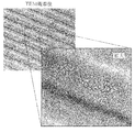
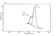
- FIG. 3 is a TEM observation photograph of the surface of the recording layer for an optical information recording medium according to the present invention. It is a Pd state analysis result (Pd 3d5 / 2 photoelectron spectrum) in Examples.
- the present inventors comprise a recording layer for a write once optical information recording medium having a higher reflectance than a conventional recording layer and excellent recording sensitivity at a practical recording laser power, and the recording layer.
- Intensive research was conducted to realize an optical information recording medium with excellent durability of the recording layer.
- the recording layer contains In oxide and Pd and the oxidation Pd contains Pd monoxide and Pd
- the oxidation layer is irradiated when the recording layer is irradiated with laser. Pd is heated by laser irradiation, decomposes and releases oxygen to change the structure of the recording layer.
- the recording method using the recording layer is different from the phase change method using the fact that the structure of the recording layer before the laser irradiation is amorphous and is amorphous after the laser irradiation. .
- the reason why the recording layer of the present invention is excellent in recording sensitivity is that the transmittance is increased (that is, the reflectance is decreased) in the portion where bubbles are generated by laser irradiation compared to the portion where bubbles are not generated. It is conceivable that the modulation degree could be increased.
- the refractive index can be increased as compared with the case where oxidized Pd is not included, and a high reflectance can be obtained. Further, since the light absorption rate of the film can be increased, the energy of the laser for signal recording can be efficiently changed to heat, and as a result, the decomposition of the oxidized Pd can be performed with a practical recording laser power. Is promoted, and the recording sensitivity can be sufficiently improved.
- the ratio of Pd atoms to the total of In atoms and Pd atoms contained in the recording layer (hereinafter sometimes referred to as “Pd amount”) needs to be 6 atomic% or more. If the amount of Pd is less than 6 atomic%, the amount of released oxygen is not sufficient because the amount of oxidized Pd that decomposes during laser irradiation is small, resulting in fewer bubbles, resulting in a lower signal intensity (C / N ratio). . Further, since the light absorption rate of the recording layer is also reduced, the laser power required for recording is increased, which is not preferable.
- the amount of Pd is preferably 8 atomic% or more, more preferably 10 atomic% or more.
- the upper limit of the amount of Pd is set to 60 atomic%.
- the upper limit of the amount of Pd is preferably 50 atomic%, more preferably 45 atomic%.
- the recording sensitivity can be improved sufficiently.
- Pd dioxide which is more unstable than monoxide Pd
- Pd dioxide is easily decomposed by laser irradiation to release oxygen, and Pd dioxide is present in the monoxide Pd that is more stable than Pd dioxide.
- the natural decomposition of Pd dioxide is suppressed and a stable recording layer can be obtained.
- the ratio of the Pd dioxide to the total of the Pd monoxide and the Pd dioxide is preferably 5 mol% or more.
- the ratio of Pd dioxide is preferably 70 mol% or less. More preferably, it is 60 mol% or less.
- the recording layer of the present invention includes an oxide of “In” in which the absolute value of the standard free energy of formation of oxide with respect to 1 mol of oxygen is larger than Pd together with the above-described oxide Pd.
- In oxide which is more stable than oxidized Pd, together with oxidized Pd, the change in form due to oxygen release when the oxidized Pd is decomposed can be made clear and large, and the recording sensitivity can be improved sufficiently. Can be made.
- the recording layer of the present invention contains In oxide, and preferably contains 50 mol% or more of In oxide.
- the recording layer of the present invention may contain unavoidable impurities in addition to the oxidized In and oxidized Pd.
- Sn, Al, Bi, Cu, Nb, Ti, Si, and Ta are contained within a total amount of about 30 atomic% or less in the state of oxide or metal for the purpose of improving the absorptance and controlling the refractive index. You may go out.
- the thickness of the recording layer depends on the structure of the optical information recording medium, such as inserting other layers such as a metal compound layer and a metal layer above and below the recording layer, but when the recording layer is used as a single layer (dielectric) Whether the body layer or the optical adjustment layer is not provided) or not, the thickness of the recording layer is preferably 5 to 100 nm.
- the film thickness of the recording layer is smaller than 5 nm, there is a tendency that a sufficient change in reflectance due to recording is difficult to obtain. More preferably, it is 10 nm or more, More preferably, it is 20 nm or more, Most preferably, it is 25 nm or more.
- the film thickness of the recording layer is larger than 100 nm, it takes time to form the film, the productivity is lowered, and the laser power required for recording tends to increase. More preferably, it is 70 nm or less, More preferably, it is 60 nm or less.
- the recording layer of the present invention contains oxidized Pd (for example, PdO, PdO 2, PdOX, etc.).
- the recording layer can be formed by sputtering.
- the sputtering method is preferable because the film thickness distribution uniformity within the disk surface can be secured.
- the ratio of the oxygen flow rate to the Ar (argon) flow rate is 0.5 to 10.0 as sputtering conditions.
- Other conditions in the sputtering method are not particularly limited, and a widely used method can be adopted.
- the gas pressure is in the range of 0.1 to 1.0 Pa, for example, and the sputtering power is in the range of 0.5 to 20 W / cm 2 , for example. What is necessary is just to control to a range.
- target As a sputtering target (hereinafter, simply referred to as “target”) used in the sputtering method, (A) Indium oxide (specifically, for example, containing 50 mol% or more of oxidized In) and Pd (eg, oxidized Pd and / or metal Pd), and with respect to the sum of In atoms and Pd atoms contained in the sputtering target A sputtering target characterized in that the ratio of Pd atoms is 6 to 60 atomic%, (B) A sputtering target having a feature in that it is made of an In-based alloy containing 6 to 60 atomic% of Pd (for example, metal Pd) in the ratio of Pd atoms to the total of In atoms and Pd atoms can be mentioned. Also, (C) A metal In target (pure In metal target) and a metal Pd target (pure Pd metal target) are used, and these are simultaneously discharged to perform multi-source sputtering
- the sputtering target of the above (A) in particular, it is possible to use a product obtained by mixing and sintering powders of oxidized In and metal Pd, and in-plane uniformity of productivity and composition of the formed thin film. It is preferable in terms of thickness control.
- the component composition of the sputtering target of the present invention does not prescribe even the trace components that are inevitably mixed, and the trace amounts of these unavoidable impurities are allowed as long as the above characteristics of the present invention are not impaired.
- the optical information recording medium of the present invention is characterized in that the recording layer is provided.
- the configuration other than the recording layer is not particularly limited, and a configuration known in the field of optical information recording media is adopted. It is also possible to provide the recording layer and the following dielectric layer formed adjacent to the recording layer.
- the optical information recording medium of the present invention has a recording layer exhibiting the above excellent characteristics, but it is also necessary to maintain the above excellent characteristics even in a high temperature and high humidity environment, that is, to ensure excellent durability. It is. Under the above environment, the oxidized Pd in the portion not irradiated with laser (that is, recording is not performed) is gradually reduced to release oxygen, resulting in a change in optical characteristics and a decrease in reflectance. Appearance is considered as a cause of the decrease in durability. However, it seems that by forming the dielectric layer adjacent to the recording layer, unnecessary decomposition of oxidized Pd (particularly Pd dioxide) in the recording layer can be suppressed and stably held.
- the above-mentioned “formation of the dielectric layer adjacent to the recording layer” includes, for example, the case where the dielectric layer is formed between the substrate and the recording layer and adjacent to the recording layer, and / or the recording layer and will be described later. A case where it is formed between the light transmission layer and adjacent to the recording layer can be mentioned.
- the dielectric layer also improves durability by acting as an oxygen barrier layer. By preventing the escape of oxygen that can be caused by unnecessary decomposition of the oxidized Pd, it is possible to prevent a change in reflectance (particularly, a decrease in reflectance), and to secure the reflectance necessary for the recording layer.
- recording characteristics can be improved by forming a dielectric layer. This is because the thermal diffusion of the laser incident by the dielectric layer is optimally controlled to prevent the bubbles in the recording portion from becoming too large or the decomposition of the oxidized Pd from proceeding too much to collapse the bubbles. This is considered to be possible to optimize.
- Examples of the material of the dielectric layer include oxides, nitrides, sulfides, carbides, fluorides, or mixtures thereof.
- Examples of the oxides include In, Zn, Sn, Al, Si, Ge, Ti, and Ta.
- the nitride is a nitride of one or more elements selected from the group consisting of In, Sn, Ge, Cr, Si, Al, Nb, Mo, Ti, and Zn (preferably Si and / or Ge nitridation).
- sulfides include Zn sulfide.
- the carbide is a carbide of one or more elements selected from the group consisting of In, Sn, Ge, Cr, Si, Al, Ti, Zr, Ta and W (preferably from the group consisting of Si, Ti and W).
- the carbide of one or more elements selected) and the fluoride include a fluoride of one or more elements selected from the group consisting of Si, Al, Mg, Ca, and La. Examples of such a mixture include ZnS—SiO2.
- the above compound (oxide or the like) containing at least one of In, Zn, Sn, Al, Si, Ti, and Mg, or a mixture thereof, and more preferable is In, Zn, Sn, The above-mentioned compound containing any one or more elements of Al or a mixture thereof.
- the film thickness of the dielectric layer is preferably 2 to 40 nm. This is because if the thickness is less than 2 nm, the effect of the dielectric layer (particularly, the effect as an oxygen barrier) is hardly exhibited. More preferably, it is 3 nm or more. On the other hand, if the dielectric layer is too thick, it is difficult for the recording layer to change (generate bubbles) due to laser irradiation, and the recording characteristics may be deteriorated. Therefore, the thickness of the dielectric layer is preferably 40 nm or less, more preferably 35 nm or less.
- the present invention does not define the method for forming the dielectric layer, but it is preferable to form the dielectric layer by the sputtering method as in the recording layer.
- the sputtering conditions are Ar flow rate, for example, in the range of 10 to 100 sccm, and when using a metal target as described below, the oxygen flow rate during oxide layer formation is For example, the range is 5 to 60 sccm, and the nitrogen flow rate when forming the nitride layer is, for example, 5 to 80 sccm.
- the gas pressure may be in the range of 0.1 to 1.0 Pa, and the sputtering power may be in the range of 0.5 to 50 W / cm 2, for example.
- a sputtering target used for forming the dielectric layer in addition to a target made of the above compound (oxide, nitride, sulfide, carbide, fluoride), other than oxygen, nitrogen, sulfur, carbon, fluorine in the compound
- a metal target containing a constituent element a target made of a pure metal or an alloy
- the configuration other than the recording layer and the dielectric layer is not particularly limited, and a configuration known in the field of optical information recording media can be adopted.
- optical information recording medium As an optical information recording medium (optical disk), a structure in which a recording layer is laminated on a substrate in which a laser guide groove is engraved, and a light transmission layer is further laminated on the substrate.
- examples of the material of the substrate include polycarbonate resin, norbornene resin, cyclic olefin copolymer, and amorphous polyolefin.
- the light transmission layer polycarbonate or ultraviolet curable resin can be used.
- the light transmission layer it is preferable that the light transmission layer has a high transmittance with respect to a laser for recording and reproduction, and has a small light absorption rate.
- the thickness of the substrate is, for example, 0.5 mm to 1.2 mm. In addition, the thickness of the light transmission layer is, for example, 0.1 mm to 1.2 mm.
- the recording layer of the present invention exhibits high reflectivity and exhibits excellent recording characteristics by itself.
- the recording layer may be above and / or below the recording layer to improve the durability of the recording layer.
- an oxide layer, a sulfide layer, a metal layer, or the like may be provided. By laminating these layers, it is possible to suppress oxidation and decomposition, which are deterioration with time of the recording layer.
- an optical adjustment layer or a dielectric layer may be provided between the substrate and the recording layer in order to further increase the reflectivity of the optical disk. Examples of the material of the optical adjustment layer include Ag, Au, Cu, Al, Ni, Cr, Ti, and alloys thereof.
- a single-layer optical disc in which one recording layer and one light transmission layer are formed is shown.
- the present invention is not limited to this, and two or more optical discs in which a plurality of recording layers and light transmission layers are stacked are shown. It may be.
- a transparent intermediate layer made of a transparent resin or the like may be included.
- a feature of the present invention is that the recording layer described above is employed.
- the optical information recording medium may be manufactured by being formed by a usual method without being particularly limited.
- the present invention is also characterized in that the recording layer described above is employed and a dielectric layer is formed adjacent to the recording layer.
- a substrate other than the recording layer and the dielectric layer and light transmission There is no particular limitation on the method of forming the layer, and further, the optical adjustment layer, the transparent intermediate layer, etc., and the optical information recording medium may be produced by forming it by a conventional method.
- optical information recording medium examples include CD, DVD, and BD.
- a BD capable of recording and reproducing data by irradiating a recording layer with blue laser light having a wavelength of about 380 nm to 450 nm, preferably about 405 nm.
- a specific example is -R.
- Example 1 Production of optical disk A polycarbonate substrate (thickness: 1.1 mm, diameter: 120 mm, track pitch: 0.32 ⁇ m, groove depth: 25 nm) was used as a disk substrate, and a DC magnetron sputtering method was used on the substrate. As shown in Table 1, recording layers having various amounts of Pd were formed. The film thickness of the recording layer was 40 nm. Sputtering was performed by simultaneously discharging a pure In metal target and a pure Pd metal target.
- the sputtering conditions for forming the recording layer were Ar flow rate: 10 sccm, oxygen flow rate: 10 sccm, gas pressure: 0.4 Pa, DC sputtering power: 100 to 200 W, and substrate temperature: room temperature.
- the component composition (Pd amount) of the formed recording layer was measured by ICP emission analysis, fluorescent X-ray analysis, or X-ray photoelectron spectroscopy.
- an ultraviolet curable resin (“BRD-864” manufactured by Nippon Kayaku Co., Ltd.) was spin-coated on the recording layer obtained as described above, and then irradiated with ultraviolet rays to have a film thickness of about 0.1 mm. A light transmission layer was formed to obtain an optical disk.
- optical disk evaluation device manufactured by Pulstec Industrial Co., Ltd., recording laser wavelength: 405 nm, NA (numerical aperture): 0.85
- the laser is irradiated onto the track and converted from the return intensity of the reflected light.
- the reflectance at a wavelength of 405 nm was determined.
- recording laser power in the range of 2 mW to 20 mW, linear velocity: 4.92 m / s, length: 0.60 ⁇ m, recording mark (Blu-ray Disc 8T signal) was repeatedly formed.
- the degree of modulation was calculated from the following formula (1) by determining the reflectance of the unrecorded portion and the reflectance of the recorded portion.
- Modulation degree (change rate of reflectance) (reflectance of unrecorded portion ⁇ reflectance of recorded portion) / (reflectance of unrecorded portion) (1)
- the reflectance is 4% or more
- the recording power (recording laser power when the highest C / N ratio is obtained) is 9 mW or less
- the C / N ratio (the highest C / N ratio) is 45 dB or more.
- those having a modulation degree of 0.40 or more were evaluated as having high reflectivity (initial reflectivity) and excellent recording sensitivity with practical recording laser power.
- the recording layer satisfying the definition of the present invention has a high reflectance and a high recording sensitivity even when the recording laser power is low.
- Example 2 An optical disc was produced and evaluated in the same manner as in Experimental Example 1 except that a recording layer having the component composition shown in Table 2 below was formed using pure Cu or pure Ag instead of pure Pd as a sputtering target. The results are shown in Table 2.
- Example 3 Except for changing the film forming gas flow rate during film formation as shown in Table 3 below, in the same manner as in Experimental Example 1, No. 1 in Table 3 was obtained. 2 optical disks were prepared and evaluated. The results are shown in Table 3. In Table 3, No. 1 is No. 1 in Table 1. Same as 5.
- Table 3 shows that the amount of oxygen contained in the recording layer is small and In and Pd are not sufficiently oxidized (No. 2), and the amount of oxygen contained in the recording layer is No. 2. No. 2 more than 2. No. 1 is compared with each other when recording is performed with the same recording power. In case of 2, there was a problem that a sufficient C / N ratio and modulation degree could not be obtained.
- FIG. 1 a TEM observation photograph of the surface of the recording layer after laser irradiation was taken with respect to those having good recording characteristics satisfying the provisions of the present invention.
- the TEM observation photograph is shown in FIG.
- FIG. 1 particularly, enlarged photograph
- those satisfying the provisions of the present invention have sufficient recording sensitivity because, as described above, the oxidized Pd in the recording layer decomposes to generate oxygen and bubbles are generated. It seems to have been raised.
- Example 4 (1) Production of optical disk A polycarbonate substrate (thickness: 1.1 mm, diameter: 120 mm, track pitch: 0.32 ⁇ m, groove depth: 25 nm) was used as a disk substrate, and a DC magnetron sputtering method was used on the substrate. Recording layers having various contents of In oxide, metal Pd, and oxide Pd (the molar ratio of Pd monoxide and Pd in the total of Pd monoxide and Pd dioxide is as shown in Table 4) did. The film thickness of the recording layer was 40 nm. Sputtering was performed by multi-source sputtering by simultaneous discharge of two targets, a pure In metal target and a pure Pd metal target.
- the sputtering conditions for forming the recording layer were constant at Ar flow rate: 10 sccm, and the oxygen flow rate introduced simultaneously with Ar was changed within the range of 5 to 50 sccm as shown in Table 4.
- the gas pressure was 0.4 Pa
- the DC sputtering power was 100 to 200 W
- the substrate temperature was room temperature.
- the component composition (Pd amount) of the formed recording layer was measured by ICP emission analysis, fluorescent X-ray analysis, or X-ray photoelectron spectroscopy.
- an ultraviolet curable resin (“BRD-864” manufactured by Nippon Kayaku Co., Ltd.) is spin-coated on the obtained recording layer, and then irradiated with ultraviolet rays to form a light transmission layer having a thickness of about 0.1 mm. Film was obtained to obtain an optical disk.
- the state analysis of Pd was performed as follows. That is, the outermost surface spectrum of the recording layer is measured by X-ray photoelectron spectroscopy (the apparatus is a Quanta SXM manufactured by Physical Electronics Co., Ltd.), and the peak separation of the Pd 3d5 / 2 photoelectron spectrum is performed. Presence form of Pd present in: The molar ratio (mol%) of metal Pd, monoxide Pd, and Pd dioxide was determined. The charge was corrected using photoelectrons from the C1s level as a reference. The analysis was performed in a state where the light transmission layer (cover layer) of the optical disc was peeled off and a recording layer was formed on the polycarbonate substrate, and the analysis region was about ⁇ 200 ⁇ m. As an example of the spectrum, No. The Pd ⁇ 3d5 / 2 photoelectron spectrum of No. 4 is shown in FIG.
- optical disc evaluation apparatus (“ODU-1000” manufactured by Pulstec Industrial Co., Ltd.) was used, a recording laser center wavelength was set to 405 nm, and a lens with NA (numerical aperture): 0.85 was used.
- NA number of NA
- Modulation degree (change rate of reflectance) (reflectance of unrecorded portion ⁇ reflectance of recorded portion) / (reflectance of unrecorded portion) (1)
- the degree of modulation is increased by the presence of Pd dioxide as the oxidized Pd, and in particular, the ratio of Pd dioxide to the total of Pd monoxide and Pd dioxide is within the recommended range. It can be seen that a high degree of modulation can be obtained. No. In No. 6, the recording power and the modulation degree could not be measured, but barely recorded, the recording power was 5.5 mW and the modulation degree was 0.15.
- Example 5 Production of optical disk A polycarbonate substrate (thickness: 1.1 mm, diameter: 120 mm, track pitch: 0.32 ⁇ m, groove depth: 25 nm) was used as a disk substrate. And in Table 5 below, No. For 3 to 5 and 9 to 12, a dielectric layer (lower) having the components and film thicknesses shown in Table 5 was formed by DC magnetron sputtering using an oxide target or a pure metal target.
- the sputtering conditions for forming this dielectric layer are: Ar flow rate: 10-30 sccm, oxygen flow rate (when using a pure metal target as a target): 0-10 sccm, gas pressure: 0.2-0.4 Pa, DC sputtering power: 100 to 400 W, substrate temperature: room temperature.
- a recording layer was formed.
- recording layers having a ratio of In atoms to Pd atoms of 60:40 were formed on the dielectric layer (lower) by a DC magnetron sputtering method.
- the film thickness of the recording layer was 40 nm.
- Sputtering was performed by multi-source sputtering by simultaneous discharge of two targets, a pure In metal target and a pure Pd metal target.
- the sputtering conditions for forming the recording layer were Ar flow rate: 10 sccm, oxygen flow rate: 15 sccm, gas pressure: 0.4 Pa, DC sputtering power: 100 to 200 W, and substrate temperature: room temperature.
- an oxide target or a pure metal target for example, ZnS—SiO 2 metal, metal Mg, metal Zn, metal Sn, metal Bi, metal Ti, etc. as a target
- a dielectric layer (upper) having the components and film thicknesses shown in Table 5 was formed.
- an ultraviolet curable resin (“BRD-864” manufactured by Nippon Kayaku Co., Ltd.) is spin-coated on the dielectric layer (top), and then irradiated with ultraviolet rays to transmit light having a thickness of about 0.1 mm. A layer was formed to obtain an optical disk.
- the recording layer contains oxidized In and oxidized Pd, and the oxidized Pd contains oxidized Pd and oxidized Pd.
- the ratio of oxidized Pd to the total of oxidized Pd and oxidized Pd is 27.8. It was confirmed separately that it was mol%.
- the Pd state analysis was performed as follows. That is, the outermost surface spectrum of the recording layer was measured by X-ray photoelectron spectroscopy (the apparatus was Quantera SXM manufactured by Physical Electronics), and the peak separation of the Pd 3d5 / 2 photoelectron spectrum was performed. Presence form of Pd present in: The molar ratio (mol%) of metal Pd, monoxide Pd, and Pd dioxide was determined. The charge was corrected using photoelectrons from the C1s level as a reference. The analysis area was about ⁇ 200 ⁇ m.
- optical disk evaluation apparatus manufactured by Pulstec Industrial Co., Ltd., recording laser wavelength: 405 nm, NA (numerical aperture): 0.85
- the laser is irradiated onto the track, and the laser beam of the unrecorded portion of the optical disk
- the reflectance (initial reflectance) at a wavelength of 405 nm was determined in terms of the return light intensity.
- Rate of change in reflectance (%) 100 ⁇ (reflectance after test [%] ⁇ initial reflectance [%]) / initial reflectance [%] (2)
- the change in reflectance can be made sufficiently smaller than when the dielectric layer is not formed, and an optical information recording medium excellent in durability can be obtained. It can be seen that it can be realized. In particular, it can be seen that by forming the dielectric layer above and below the recording layer, the rate of change in reflectivity is remarkably reduced and the durability is excellent.
- a recording layer for a write once optical information recording medium having a high reflectance (initial reflectance) and excellent recording sensitivity at a practical recording laser power, and the recording layer are provided.
- a write-once optical information recording medium having excellent layer durability can be provided.
- a sputtering target useful for forming the recording layer can be provided.
Abstract
A recording layer for an optical information recording medium, which has a high reflectance (initial reflectance) and excellent recording characteristics; an optical information recording medium comprising the recording layer; and a sputtering target useful for forming the recording layer. The recording layer for an optical information recording medium, on which recording is performed by irradiation of laser light, is characterized by containing indium (In) oxide and palladium (Pd) oxide which includes palladium monoxide and palladium dioxide. The recording layer for an optical information recording medium is also characterized in that the ratio of Pd atoms contained in the recording layer relative to the total of In atoms and Pd atoms contained therein is 6-60 atom%.
Description
本発明は、光情報記録媒体用の記録層、光情報記録媒体、および該記録層の形成に有用なスパッタリングターゲットに関するものである。
The present invention relates to a recording layer for an optical information recording medium, an optical information recording medium, and a sputtering target useful for forming the recording layer.
光情報記録媒体(光ディスク)は、CD、DVD、BDといった光ディスクに代表され、記録再生方式により、再生専用型、追記型および書換え型の3種類に大別される。このうち追記型の光ディスクの記録方式は、主に、記録層を相変化させる相変化方式、複数の記録層を反応させる層間反応方式、記録層を構成する化合物を分解させる方式、記録層に孔やピットなどの記録マークを局所的に形成させる孔開け方式に大別される。
Optical information recording media (optical discs) are typified by optical discs such as CDs, DVDs, and BDs, and are roughly classified into three types according to the recording / reproducing method: read-only type, write once type, and rewritable type. Of these, the write-once type optical disc recording method mainly includes a phase change method for changing the phase of the recording layer, an interlayer reaction method for reacting a plurality of recording layers, a method for decomposing a compound constituting the recording layer, and a hole in the recording layer. It is roughly classified into a drilling method in which recording marks such as pits are locally formed.
前記相変化方式では、記録層の結晶化による光学特性の変化を利用した材料が、記録層の材料として提案されている。例えば特許文献1では、Te-O-M(Mは金属元素、半金属元素及び半導体元素から選ばれる少なくとも1種の元素)を含む記録層が提案され、特許文献2ではSbおよびTeを含む記録層が提案されている。
In the phase change method, a material using a change in optical characteristics due to crystallization of the recording layer has been proposed as a material for the recording layer. For example, Patent Document 1 proposes a recording layer containing Te—OM (where M is at least one element selected from a metal element, a metalloid element, and a semiconductor element), and Patent Document 2 proposes a recording layer containing Sb and Te. Layers have been proposed.
前記層間反応方式の光情報記録媒体の記録層としては、例えば特許文献3に、第一記録層をIn-O-(Ni、Mn、Mo)を含む合金からなるものとし、かつ第二記録層をSe及び/又はTe元素、O(酸素)、及びTi、Pd、Zrの中から選ばれた一つの元素を含む合金からなるものとした記録層が提案されている。また特許文献4では、第一記録層:Inを主成分とする金属、第二記録層:5B族または6B族に属する少なくとも1種類の元素を含む、酸化物以外の金属あるいは非金属を積層して、加熱による反応または合金化により記録を行うことが提案されている。
As the recording layer of the interlayer reaction type optical information recording medium, for example, in Patent Document 3, the first recording layer is made of an alloy containing In—O— (Ni, Mn, Mo), and the second recording layer is used. Has been proposed that is made of an alloy containing Se and / or Te element, O (oxygen), and one element selected from Ti, Pd, and Zr. Further, in Patent Document 4, a first recording layer: a metal containing In as a main component, and a second recording layer: a metal other than an oxide or a nonmetal containing at least one element belonging to Group 5B or Group 6B are stacked. Thus, it has been proposed to perform recording by reaction or alloying by heating.
前記記録層を構成する化合物を分解する方式の記録層として、例えば特許文献5には、窒化物を主成分とした記録層が示されており、該窒化物を加熱により分解することで記録を行う材料や、有機色素材料が検討されている。
As a recording layer of a method for decomposing a compound constituting the recording layer, for example, Patent Document 5 shows a recording layer mainly composed of nitride, and recording can be performed by decomposing the nitride by heating. Materials to be performed and organic pigment materials are being studied.
前記孔開け方式の記録層としては、低融点金属材料からなるものが検討されている。例えば特許文献6では、Sn合金に3B族、4B族、5B族の元素を添加した合金からなるものが提案され、本願出願人も特許文献7にて、Niおよび/またはCoを1~50原子%の範囲で含有するSn基合金からなる記録層を提案している。また本願出願人は、特許文献8で、Coを20~65原子%含有するIn合金、さらにこれにSn、Bi、Ge、Siから選ばれる1種類以上の元素を19原子%以下含有するIn合金からなる記録層を提案している。
As the perforated recording layer, a recording layer made of a low melting point metal material has been studied. For example, Patent Document 6 proposes an alloy formed by adding an element of 3B group, 4B group, or 5B group to an Sn alloy, and the applicant of the present application also disclosed 1 to 50 atoms of Ni and / or Co in Patent Document 7. %, A recording layer made of an Sn-based alloy is proposed. In addition, the applicant of the present application disclosed in Patent Document 8 that an In alloy containing 20 to 65 atomic percent of Co, and an In alloy containing 19 atomic percent or less of one or more elements selected from Sn, Bi, Ge, and Si. A recording layer consisting of
光情報記録媒体に求められる要求特性として、主に、再生に十分な反射率を有すること、実用的な記録レーザーパワーで記録が可能なこと(高記録感度を有すること)、記録信号が再生に十分な信号振幅を有すること(高変調度であること)、および信号強度が高いこと(高C/N比であること)が求められる。
The required characteristics required for optical information recording media are mainly that it has sufficient reflectivity for reproduction, recording with practical recording laser power (high recording sensitivity), and recording signal for reproduction. It is required to have sufficient signal amplitude (high modulation degree) and high signal strength (high C / N ratio).
しかし、従来技術として開示されている記録材料は、これらすべての要求特性を記録材料単体で満たすことが難しく、前記相変化方式では、記録層単独での反射率が低いため、光ディスク状態での反射率を高めるべく反射膜が必要であり、かつ変調度を増加させるため、記録層の上下にZnS-SiO2 などの誘電体層を設ける必要があり、光ディスクを構成する層数が多くなる。また、前記層間反応方式でも複数の記録層が必要であることから、光ディスクを構成する層数が多くなる。このため膜層数が多くなり生産性が低下するという課題がある。これに対し前記孔開け方式は、記録層自体の反射率が高く、且つ、大きな変調度も確保できるため、光ディスクを構成する層の数を低減できるが、より高い記録感度を達成するにあたっては、更なる検討が必要であることがわかった。また更には、上記記録層の耐久性(特には、高温高湿に対する耐久性)も必要である。
However, it is difficult for the recording material disclosed as the prior art to satisfy all of the required characteristics with the recording material alone. In the phase change method, since the reflectance of the recording layer alone is low, the reflection in the optical disk state is difficult. In order to increase the rate, a reflective film is required, and in order to increase the degree of modulation, it is necessary to provide dielectric layers such as ZnS—SiO 2 に above and below the recording layer, and the number of layers constituting the optical disk increases. In addition, since the interlayer reaction method also requires a plurality of recording layers, the number of layers constituting the optical disk increases. For this reason, there is a problem that the number of film layers increases and productivity decreases. On the other hand, the perforation method has a high reflectivity of the recording layer itself and can secure a large degree of modulation, so that the number of layers constituting the optical disk can be reduced, but in achieving higher recording sensitivity, It turns out that further study is needed. Furthermore, durability of the recording layer (particularly durability against high temperature and high humidity) is also required.
本発明はこの様な事情に鑑みてなされたものであって、その目的は、光ディスクの層数を低減しながら上記要求特性を満たして、光情報記録媒体の生産性を高めることのできる光情報記録媒体用記録層と、該記録層を備えた光情報記録媒体、および該記録層の形成に有用なスパッタリングターゲットを提供することにある。
The present invention has been made in view of such circumstances, and an object of the present invention is to provide optical information capable of increasing the productivity of an optical information recording medium by satisfying the above required characteristics while reducing the number of layers of an optical disk. The object is to provide a recording layer for a recording medium, an optical information recording medium provided with the recording layer, and a sputtering target useful for forming the recording layer.
本発明の要旨を以下に示す。
(1)レーザー光の照射により記録が行われる光情報記録媒体用記録層であって、
前記記録層は、酸化Inと酸化Pdとを含み、該酸化Pdが一酸化Pdと二酸化Pdを含むものであり、かつ、記録層に含まれるIn原子とPd原子の合計に対するPd原子の比率が6~60原子%である光情報記録媒体用記録層。
(2)前記一酸化Pdと二酸化Pdの合計に対する二酸化Pdの比率が、5~70モル%である(1)に記載の光情報記録媒体用記録層。
(3)膜厚が5~100nmである(1)または(2)に記載の光情報記録媒体用記録層。
(4)レーザー光の照射された部分に気泡が生成することにより記録が行われる(1)~(3)のいずれかに記載の光情報記録媒体用記録層。
(5)(1)~(4)のいずれかに記載の光情報記録媒体用記録層を備えている光情報記録媒体。
(6)レーザー光の照射により記録が行われる記録層と、該記録層に隣接して形成される誘電体層とを備えた光情報記録媒体であって、
前記記録層は、酸化Inと酸化Pdを含み、該酸化Pdが一酸化Pdと二酸化Pdを含むものであり、かつ、記録層に含まれるIn原子とPd原子の合計に対するPd原子の比率が6~60原子%である光情報記録媒体。
(7)前記記録層に含まれる一酸化Pdと二酸化Pdの合計に対する二酸化Pdの比率が、5~70モル%である(6)に記載の光情報記録媒体。
(8)前記誘電体層が、酸化物、窒化物、硫化物、炭化物、またはその混合物を含む(6)または(7)に記載の光情報記録媒体。
(9)前記誘電体層に含まれる、前記酸化物はIn、Zn、Sn、Al、Si、Ge、Ti、Ta、Nb、Hf、Zr、Cr、BiおよびMgよりなる群から選択される1種以上の元素の酸化物であり、前記窒化物はSiおよびGeの少なくとも一つの窒化物であり、前記硫化物はZn硫化物であり、前記炭化物はSi、TiおよびWよりなる群から選択される1種以上の元素の炭化物である(8)に記載の光情報記録媒体。
(10)前記誘電体層の膜厚が2~40nmである(6)~(9)のいずれかに記載の光情報記録媒体。
(11)前記記録層の膜厚が5~100nmである(6)~(10)のいずれかに記載の光情報記録媒体。
(12)前記記録層におけるレーザー光の照射された部分に、気泡が生成することにより記録が行われる(6)~(11)のいずれかに記載の光情報記録媒体。
(13)(1)~(4)のいずれかに記載の光情報記録媒体用記録層を形成するためのスパッタリングターゲットであって、
酸化InとPdを含み(好ましくは酸化Inを主体としてPdを含み)、かつ、スパッタリングターゲットに含まれるIn原子とPd原子の合計に対するPd原子の比率が6~60原子%(好ましくは6~50原子%)であるスパッタリングターゲット。
(14)(1)~(4)のいずれかに記載の光情報記録媒体用記録層を形成するためのスパッタリングターゲットであって、
In原子とPd原子の合計に対するPd原子の比率で6~60原子%(好ましくは6~50原子%)のPdを含むIn基合金から実質的になるスパッタリングターゲット。
なお、上記(4)の光情報記録媒体用記録層は、レーザー光の照射された部分に気泡が生成し、体積変化することにより記録が行われる(1)~(3)のいずれかに記載の光情報記録媒体用記録層であることが好ましい。
上記(8)の光情報記録媒体は、前記誘電体層が、酸化物、窒化物、硫化物、炭化物、またはその混合物からなる(6)または(7)に記載の光情報記録媒体であることが好ましい。
上記(9)の光情報記録媒体は、前記誘電体層を構成する、前記酸化物はIn、Zn、Sn、Al、Si、Ge、Ti、Ta、Nb、Hf、Zr、Cr、BiおよびMgよりなる群から選択される1種以上の元素の酸化物であり、前記窒化物はSiおよびGeの少なくとも一つの窒化物であり、前記硫化物はZn硫化物であり、前記炭化物はSi、TiおよびWよりなる群から選択される1種以上の元素の炭化物である(8)に記載の光情報記録媒体であることが好ましい。
上記(12)の光情報記録媒体は、前記記録層におけるレーザー光の照射された部分に、気泡が生成し、体積変化することにより記録が行われる(6)~(11)のいずれかに記載の光情報記録媒体であることが好ましい。
上記(14)のスパッタリングターゲットは、(1)~(4)のいずれかに記載の光情報記録媒体用記録層を形成するためのスパッタリングターゲットであって、In原子とPd原子の合計に対するPd原子の比率で6~60原子%(好ましくは6~50原子%)のPdを含むIn基合金からなるスパッタリングターゲットであることが好ましい。 The gist of the present invention is shown below.
(1) A recording layer for an optical information recording medium on which recording is performed by laser light irradiation,
The recording layer contains In oxide and Pd oxide, the oxide Pd contains Pd monoxide and Pd dioxide, and the ratio of Pd atoms to the total of In atoms and Pd atoms contained in the recording layer is A recording layer for an optical information recording medium of 6 to 60 atomic%.
(2) The recording layer for optical information recording media according to (1), wherein the ratio of Pd dioxide to the total of Pd monoxide and Pd is 5 to 70 mol%.
(3) The recording layer for optical information recording media according to (1) or (2), wherein the film thickness is 5 to 100 nm.
(4) The recording layer for an optical information recording medium according to any one of (1) to (3), wherein recording is performed by generating bubbles in a portion irradiated with laser light.
(5) An optical information recording medium comprising the optical information recording medium recording layer according to any one of (1) to (4).
(6) An optical information recording medium comprising a recording layer on which recording is performed by laser light irradiation, and a dielectric layer formed adjacent to the recording layer,
The recording layer contains In oxide and Pd oxide, the oxide Pd contains Pd monoxide and Pd dioxide, and the ratio of Pd atoms to the total of In atoms and Pd atoms contained in the recording layer is 6 An optical information recording medium of ˜60 atomic%.
(7) The optical information recording medium according to (6), wherein the ratio of Pd dioxide to the total of Pd monoxide and Pd contained in the recording layer is 5 to 70 mol%.
(8) The optical information recording medium according to (6) or (7), wherein the dielectric layer includes an oxide, a nitride, a sulfide, a carbide, or a mixture thereof.
(9) The oxide contained in the dielectric layer is selected from the group consisting of In, Zn, Sn, Al, Si, Ge, Ti, Ta, Nb, Hf, Zr, Cr, Bi, andMg 1 An oxide of at least one element, the nitride is at least one nitride of Si and Ge, the sulfide is Zn sulfide, and the carbide is selected from the group consisting of Si, Ti and W The optical information recording medium according to (8), which is a carbide of one or more elements.
(10) The optical information recording medium according to any one of (6) to (9), wherein the dielectric layer has a thickness of 2 to 40 nm.
(11) The optical information recording medium according to any one of (6) to (10), wherein the recording layer has a thickness of 5 to 100 nm.
(12) The optical information recording medium according to any one of (6) to (11), wherein recording is performed by generating bubbles in a portion irradiated with laser light in the recording layer.
(13) A sputtering target for forming the recording layer for an optical information recording medium according to any one of (1) to (4),
It contains In oxide and Pd (preferably mainly containing In oxide and Pd), and the ratio of Pd atoms to the total of In atoms and Pd atoms contained in the sputtering target is 6 to 60 atomic% (preferably 6 to 50%). Sputtering target that is atomic%).
(14) A sputtering target for forming a recording layer for an optical information recording medium according to any one of (1) to (4),
A sputtering target consisting essentially of an In-based alloy containing 6 to 60 atomic% (preferably 6 to 50 atomic%) of Pd in a ratio of Pd atoms to the total of In atoms and Pd atoms.
In the recording layer for optical information recording medium of (4) above, recording is performed by generating bubbles in the portion irradiated with the laser beam and changing the volume, (1) to (3) The recording layer for an optical information recording medium is preferable.
(8) The optical information recording medium according to (6) or (7), wherein the dielectric layer is made of an oxide, nitride, sulfide, carbide, or a mixture thereof. Is preferred.
The optical information recording medium of (9) above constitutes the dielectric layer, and the oxide is In, Zn, Sn, Al, Si, Ge, Ti, Ta, Nb, Hf, Zr, Cr, Bi, and Mg. An oxide of at least one element selected from the group consisting of: the nitride is at least one nitride of Si and Ge; the sulfide is Zn sulfide; and the carbide is Si, Ti. And the optical information recording medium according to (8), which is a carbide of one or more elements selected from the group consisting of W and W.
In the optical information recording medium of (12), recording is performed by generating bubbles in the portion of the recording layer irradiated with laser light and changing the volume thereof. The optical information recording medium is preferable.
The sputtering target (14) is a sputtering target for forming the recording layer for an optical information recording medium according to any one of (1) to (4), wherein Pd atoms relative to the sum of In atoms and Pd atoms A sputtering target made of an In-based alloy containing 6 to 60 atomic% (preferably 6 to 50 atomic%) of Pd is preferable.
(1)レーザー光の照射により記録が行われる光情報記録媒体用記録層であって、
前記記録層は、酸化Inと酸化Pdとを含み、該酸化Pdが一酸化Pdと二酸化Pdを含むものであり、かつ、記録層に含まれるIn原子とPd原子の合計に対するPd原子の比率が6~60原子%である光情報記録媒体用記録層。
(2)前記一酸化Pdと二酸化Pdの合計に対する二酸化Pdの比率が、5~70モル%である(1)に記載の光情報記録媒体用記録層。
(3)膜厚が5~100nmである(1)または(2)に記載の光情報記録媒体用記録層。
(4)レーザー光の照射された部分に気泡が生成することにより記録が行われる(1)~(3)のいずれかに記載の光情報記録媒体用記録層。
(5)(1)~(4)のいずれかに記載の光情報記録媒体用記録層を備えている光情報記録媒体。
(6)レーザー光の照射により記録が行われる記録層と、該記録層に隣接して形成される誘電体層とを備えた光情報記録媒体であって、
前記記録層は、酸化Inと酸化Pdを含み、該酸化Pdが一酸化Pdと二酸化Pdを含むものであり、かつ、記録層に含まれるIn原子とPd原子の合計に対するPd原子の比率が6~60原子%である光情報記録媒体。
(7)前記記録層に含まれる一酸化Pdと二酸化Pdの合計に対する二酸化Pdの比率が、5~70モル%である(6)に記載の光情報記録媒体。
(8)前記誘電体層が、酸化物、窒化物、硫化物、炭化物、またはその混合物を含む(6)または(7)に記載の光情報記録媒体。
(9)前記誘電体層に含まれる、前記酸化物はIn、Zn、Sn、Al、Si、Ge、Ti、Ta、Nb、Hf、Zr、Cr、BiおよびMgよりなる群から選択される1種以上の元素の酸化物であり、前記窒化物はSiおよびGeの少なくとも一つの窒化物であり、前記硫化物はZn硫化物であり、前記炭化物はSi、TiおよびWよりなる群から選択される1種以上の元素の炭化物である(8)に記載の光情報記録媒体。
(10)前記誘電体層の膜厚が2~40nmである(6)~(9)のいずれかに記載の光情報記録媒体。
(11)前記記録層の膜厚が5~100nmである(6)~(10)のいずれかに記載の光情報記録媒体。
(12)前記記録層におけるレーザー光の照射された部分に、気泡が生成することにより記録が行われる(6)~(11)のいずれかに記載の光情報記録媒体。
(13)(1)~(4)のいずれかに記載の光情報記録媒体用記録層を形成するためのスパッタリングターゲットであって、
酸化InとPdを含み(好ましくは酸化Inを主体としてPdを含み)、かつ、スパッタリングターゲットに含まれるIn原子とPd原子の合計に対するPd原子の比率が6~60原子%(好ましくは6~50原子%)であるスパッタリングターゲット。
(14)(1)~(4)のいずれかに記載の光情報記録媒体用記録層を形成するためのスパッタリングターゲットであって、
In原子とPd原子の合計に対するPd原子の比率で6~60原子%(好ましくは6~50原子%)のPdを含むIn基合金から実質的になるスパッタリングターゲット。
なお、上記(4)の光情報記録媒体用記録層は、レーザー光の照射された部分に気泡が生成し、体積変化することにより記録が行われる(1)~(3)のいずれかに記載の光情報記録媒体用記録層であることが好ましい。
上記(8)の光情報記録媒体は、前記誘電体層が、酸化物、窒化物、硫化物、炭化物、またはその混合物からなる(6)または(7)に記載の光情報記録媒体であることが好ましい。
上記(9)の光情報記録媒体は、前記誘電体層を構成する、前記酸化物はIn、Zn、Sn、Al、Si、Ge、Ti、Ta、Nb、Hf、Zr、Cr、BiおよびMgよりなる群から選択される1種以上の元素の酸化物であり、前記窒化物はSiおよびGeの少なくとも一つの窒化物であり、前記硫化物はZn硫化物であり、前記炭化物はSi、TiおよびWよりなる群から選択される1種以上の元素の炭化物である(8)に記載の光情報記録媒体であることが好ましい。
上記(12)の光情報記録媒体は、前記記録層におけるレーザー光の照射された部分に、気泡が生成し、体積変化することにより記録が行われる(6)~(11)のいずれかに記載の光情報記録媒体であることが好ましい。
上記(14)のスパッタリングターゲットは、(1)~(4)のいずれかに記載の光情報記録媒体用記録層を形成するためのスパッタリングターゲットであって、In原子とPd原子の合計に対するPd原子の比率で6~60原子%(好ましくは6~50原子%)のPdを含むIn基合金からなるスパッタリングターゲットであることが好ましい。 The gist of the present invention is shown below.
(1) A recording layer for an optical information recording medium on which recording is performed by laser light irradiation,
The recording layer contains In oxide and Pd oxide, the oxide Pd contains Pd monoxide and Pd dioxide, and the ratio of Pd atoms to the total of In atoms and Pd atoms contained in the recording layer is A recording layer for an optical information recording medium of 6 to 60 atomic%.
(2) The recording layer for optical information recording media according to (1), wherein the ratio of Pd dioxide to the total of Pd monoxide and Pd is 5 to 70 mol%.
(3) The recording layer for optical information recording media according to (1) or (2), wherein the film thickness is 5 to 100 nm.
(4) The recording layer for an optical information recording medium according to any one of (1) to (3), wherein recording is performed by generating bubbles in a portion irradiated with laser light.
(5) An optical information recording medium comprising the optical information recording medium recording layer according to any one of (1) to (4).
(6) An optical information recording medium comprising a recording layer on which recording is performed by laser light irradiation, and a dielectric layer formed adjacent to the recording layer,
The recording layer contains In oxide and Pd oxide, the oxide Pd contains Pd monoxide and Pd dioxide, and the ratio of Pd atoms to the total of In atoms and Pd atoms contained in the recording layer is 6 An optical information recording medium of ˜60 atomic%.
(7) The optical information recording medium according to (6), wherein the ratio of Pd dioxide to the total of Pd monoxide and Pd contained in the recording layer is 5 to 70 mol%.
(8) The optical information recording medium according to (6) or (7), wherein the dielectric layer includes an oxide, a nitride, a sulfide, a carbide, or a mixture thereof.
(9) The oxide contained in the dielectric layer is selected from the group consisting of In, Zn, Sn, Al, Si, Ge, Ti, Ta, Nb, Hf, Zr, Cr, Bi, and
(10) The optical information recording medium according to any one of (6) to (9), wherein the dielectric layer has a thickness of 2 to 40 nm.
(11) The optical information recording medium according to any one of (6) to (10), wherein the recording layer has a thickness of 5 to 100 nm.
(12) The optical information recording medium according to any one of (6) to (11), wherein recording is performed by generating bubbles in a portion irradiated with laser light in the recording layer.
(13) A sputtering target for forming the recording layer for an optical information recording medium according to any one of (1) to (4),
It contains In oxide and Pd (preferably mainly containing In oxide and Pd), and the ratio of Pd atoms to the total of In atoms and Pd atoms contained in the sputtering target is 6 to 60 atomic% (preferably 6 to 50%). Sputtering target that is atomic%).
(14) A sputtering target for forming a recording layer for an optical information recording medium according to any one of (1) to (4),
A sputtering target consisting essentially of an In-based alloy containing 6 to 60 atomic% (preferably 6 to 50 atomic%) of Pd in a ratio of Pd atoms to the total of In atoms and Pd atoms.
In the recording layer for optical information recording medium of (4) above, recording is performed by generating bubbles in the portion irradiated with the laser beam and changing the volume, (1) to (3) The recording layer for an optical information recording medium is preferable.
(8) The optical information recording medium according to (6) or (7), wherein the dielectric layer is made of an oxide, nitride, sulfide, carbide, or a mixture thereof. Is preferred.
The optical information recording medium of (9) above constitutes the dielectric layer, and the oxide is In, Zn, Sn, Al, Si, Ge, Ti, Ta, Nb, Hf, Zr, Cr, Bi, and Mg. An oxide of at least one element selected from the group consisting of: the nitride is at least one nitride of Si and Ge; the sulfide is Zn sulfide; and the carbide is Si, Ti. And the optical information recording medium according to (8), which is a carbide of one or more elements selected from the group consisting of W and W.
In the optical information recording medium of (12), recording is performed by generating bubbles in the portion of the recording layer irradiated with laser light and changing the volume thereof. The optical information recording medium is preferable.
The sputtering target (14) is a sputtering target for forming the recording layer for an optical information recording medium according to any one of (1) to (4), wherein Pd atoms relative to the sum of In atoms and Pd atoms A sputtering target made of an In-based alloy containing 6 to 60 atomic% (preferably 6 to 50 atomic%) of Pd is preferable.
本発明によれば、反射率(初期反射率)が高く、かつ実用的な記録レーザーパワーでの記録感度に優れた追記型光情報記録媒体用記録層、および該記録層を備えると共に、この記録層の耐久性に優れた追記型光情報記録媒体を提供することができる。また、本発明によれば、上記記録層の形成に有用なスパッタリングターゲットを提供することができる。
According to the present invention, a recording layer for a write once optical information recording medium having a high reflectance (initial reflectance) and excellent recording sensitivity at a practical recording laser power, and the recording layer are provided. A write-once optical information recording medium having excellent layer durability can be provided. Moreover, according to the present invention, a sputtering target useful for forming the recording layer can be provided.
尚、本明細書において、「記録感度に優れる」とは、後記する実施例の欄で詳述する通り、比較的低い記録レーザーパワーで高C/N比(carrier to noiseratio、読み取り時の信号とバックグラウンドのノイズの出力レベルの比)および高変調度を実現できることを意味する。
In the present specification, “excellent recording sensitivity” means a high C / N ratio (carrier-to-noise ratio, a signal at the time of reading) with a relatively low recording laser power, as will be described in detail in the section of the embodiment described later. This means that the ratio of the background noise output level) and a high degree of modulation can be realized.
本発明者らは、従来の記録層よりも、反射率が高く、かつ実用的な記録レーザーパワーでの記録感度に優れた追記型光情報記録媒体用記録層、および該記録層を備えると共に、この記録層の耐久性に優れた光情報記録媒体を実現すべく鋭意研究を行った。その結果、従来の記録層とは異なり、酸化Inと酸化Pdを含み、該酸化Pdが一酸化Pdと二酸化Pdを含む記録層とすれば、該記録層にレーザーが照射したときに、前記酸化Pdが、レーザー照射により加熱され、分解し酸素を放出して記録層の組織を変化させる、具体的には、レーザーが照射された部分に気泡を生成させて不可逆的な記録を行う方式が、従来よりも記録感度を格段に高めうること、また、誘電体層を上記記録層に隣接して形成すれば、この記録層の耐久性を格段に高めうることを見出した。
The present inventors comprise a recording layer for a write once optical information recording medium having a higher reflectance than a conventional recording layer and excellent recording sensitivity at a practical recording laser power, and the recording layer. Intensive research was conducted to realize an optical information recording medium with excellent durability of the recording layer. As a result, unlike the conventional recording layer, if the recording layer contains In oxide and Pd and the oxidation Pd contains Pd monoxide and Pd, the oxidation layer is irradiated when the recording layer is irradiated with laser. Pd is heated by laser irradiation, decomposes and releases oxygen to change the structure of the recording layer. Specifically, a method of performing irreversible recording by generating bubbles in a portion irradiated with the laser, It has been found that the recording sensitivity can be remarkably increased as compared with the conventional case, and that the durability of the recording layer can be remarkably improved if the dielectric layer is formed adjacent to the recording layer.
上記記録層による記録方式では、レーザー照射前の記録層の構造はアモルファスであり、レーザー照射後もアモルファスである点で、アモルファスがレーザー照射により結晶に変化することを利用した相変化方式と相違する。
The recording method using the recording layer is different from the phase change method using the fact that the structure of the recording layer before the laser irradiation is amorphous and is amorphous after the laser irradiation. .
本発明の記録層が記録感度に優れている理由として、レーザー照射により気泡が発生した部分では、気泡の発生していない部分と比べて透過率が増加(即ち、反射率が低下)することで、変調度を大きくすることができたことが考えられる。
The reason why the recording layer of the present invention is excellent in recording sensitivity is that the transmittance is increased (that is, the reflectance is decreased) in the portion where bubbles are generated by laser irradiation compared to the portion where bubbles are not generated. It is conceivable that the modulation degree could be increased.
また、上記の通り酸化Pdを含有させることにより、酸化Pdを含まない場合に比べて屈折率を大きくすることができ、高い反射率を得ることができる。更には、膜の光吸収率を大きくすることができるため、信号記録のためのレーザーのエネルギーを効率的に熱に変えることができ、結果として、実用的な記録レーザーパワーで上記酸化Pdの分解が促進されて、記録感度を十分に向上させることができる。
Further, by containing oxidized Pd as described above, the refractive index can be increased as compared with the case where oxidized Pd is not included, and a high reflectance can be obtained. Further, since the light absorption rate of the film can be increased, the energy of the laser for signal recording can be efficiently changed to heat, and as a result, the decomposition of the oxidized Pd can be performed with a practical recording laser power. Is promoted, and the recording sensitivity can be sufficiently improved.
これらの効果を十分発現させるには、記録層に含まれるIn原子とPd原子との合計に対するPd原子の比率(以下「Pd量」ということがある)を6原子%以上とする必要がある。Pd量が6原子%を下回ると、レーザー照射時に分解する酸化Pdが少ないため、放出される酸素量が十分でなく生成する気泡が少なくなり、結果として信号強度(C/N比)が小さくなる。また記録層の光吸収率も小さくなるため、記録に必要なレーザーパワーが大きくなり好ましくない。前記Pd量は、好ましくは8原子%以上、より好ましくは10原子%以上である。
In order to fully exhibit these effects, the ratio of Pd atoms to the total of In atoms and Pd atoms contained in the recording layer (hereinafter sometimes referred to as “Pd amount”) needs to be 6 atomic% or more. If the amount of Pd is less than 6 atomic%, the amount of released oxygen is not sufficient because the amount of oxidized Pd that decomposes during laser irradiation is small, resulting in fewer bubbles, resulting in a lower signal intensity (C / N ratio). . Further, since the light absorption rate of the recording layer is also reduced, the laser power required for recording is increased, which is not preferable. The amount of Pd is preferably 8 atomic% or more, more preferably 10 atomic% or more.
一方、前記Pd量が60原子%を超えると、変調度が小さくなるため、本発明ではPd量の上限を60原子%とした。前記Pd量の上限は、好ましくは50原子%、より好ましくは45原子%である。
On the other hand, when the amount of Pd exceeds 60 atomic%, the degree of modulation becomes small. Therefore, in the present invention, the upper limit of the amount of Pd is set to 60 atomic%. The upper limit of the amount of Pd is preferably 50 atomic%, more preferably 45 atomic%.
上記酸化Pdを、特に一酸化Pdと二酸化Pdを含むものとすれば、記録感度をより十分に向上させることができる。その理由として、一酸化Pdよりも不安定な二酸化Pdが、レーザー照射により容易に分解して酸素を放出すること、および、二酸化Pdに比べて安定な一酸化Pd中に二酸化Pdを存在させることで、この二酸化Pdの自然分解が抑制されて、安定な記録層が得られることが考えられる。
If the oxidized Pd contains, in particular, Pd monoxide and Pd dioxide, the recording sensitivity can be improved sufficiently. The reason is that Pd dioxide, which is more unstable than monoxide Pd, is easily decomposed by laser irradiation to release oxygen, and Pd dioxide is present in the monoxide Pd that is more stable than Pd dioxide. Thus, it is conceivable that the natural decomposition of Pd dioxide is suppressed and a stable recording layer can be obtained.
上記二酸化Pdの分解による酸素放出量を高めて、記録感度をより十分に向上させるには、前記一酸化Pdと二酸化Pdの合計に対する二酸化Pdの比率を、5モル%以上とすることが好ましい。一方、一酸化Pdに対し二酸化Pdが多過ぎると、二酸化Pdは安定的に存在することができず、記録層の作製が困難となるおそれがあるため、前記一酸化Pdと二酸化Pdの合計に対する二酸化Pdの比率は70モル%以下とすることが好ましい。より好ましくは60モル%以下である。
In order to increase the amount of oxygen released by the decomposition of the Pd dioxide and improve the recording sensitivity more sufficiently, the ratio of the Pd dioxide to the total of the Pd monoxide and the Pd dioxide is preferably 5 mol% or more. On the other hand, if there is too much Pd dioxide relative to Pd monoxide, Pd dioxide cannot exist stably and it may be difficult to produce a recording layer. The ratio of Pd dioxide is preferably 70 mol% or less. More preferably, it is 60 mol% or less.
本発明の記録層は、上記酸化Pdと共に、酸素1molに対する酸化物の標準生成自由エネルギーの絶対値がPdよりも大きい「In」の酸化物を含むものである。この様に、酸化Pdよりも安定な酸化Inを酸化Pdと共に含有させることによって、該酸化Pdが分解したときの酸素放出による形態変化を明瞭かつ大きくすることができ、記録感度をより十分に向上させることができる。
The recording layer of the present invention includes an oxide of “In” in which the absolute value of the standard free energy of formation of oxide with respect to 1 mol of oxygen is larger than Pd together with the above-described oxide Pd. In this way, by containing In oxide, which is more stable than oxidized Pd, together with oxidized Pd, the change in form due to oxygen release when the oxidized Pd is decomposed can be made clear and large, and the recording sensitivity can be improved sufficiently. Can be made.
本発明の記録層は、上記の通り酸化Inを含むものであり、好ましくは酸化Inを50mol%以上含むものである。尚、本発明の記録層には、該酸化Inと酸化Pdとを含む他、不可避不純物が含まれ得る。また、吸収率の向上や屈折率の制御を目的として、Sn、Al、Bi、Cu、Nb、Ti、Si、Taを、酸化物または金属の状態で合計約30原子%以下の範囲内で含んでいてもよい。
As described above, the recording layer of the present invention contains In oxide, and preferably contains 50 mol% or more of In oxide. The recording layer of the present invention may contain unavoidable impurities in addition to the oxidized In and oxidized Pd. In addition, Sn, Al, Bi, Cu, Nb, Ti, Si, and Ta are contained within a total amount of about 30 atomic% or less in the state of oxide or metal for the purpose of improving the absorptance and controlling the refractive index. You may go out.
記録層の膜厚は、記録層の上下に金属化合物層や金属層等の他の層を挿入するなど、光情報記録媒体の構造にもよるが、記録層を単層で使用する場合(誘電体層や光学調整層を設けない場合)でもそうでない場合でも、記録層の膜厚を5~100nmとすることが好ましい。記録層の膜厚が5nmより小さいと、記録による十分な反射率変化が得られにくい傾向がある。より好ましくは10nm以上、更に好ましくは20nm以上、特に好ましくは25nm以上である。一方、記録層の膜厚が100nmより大きいと、膜の形成に時間がかかり、生産性が低下すると共に、記録に必要なレーザーパワーが大きくなる傾向がある。より好ましくは70nm以下、更に好ましくは60nm以下である。
The thickness of the recording layer depends on the structure of the optical information recording medium, such as inserting other layers such as a metal compound layer and a metal layer above and below the recording layer, but when the recording layer is used as a single layer (dielectric) Whether the body layer or the optical adjustment layer is not provided) or not, the thickness of the recording layer is preferably 5 to 100 nm. When the film thickness of the recording layer is smaller than 5 nm, there is a tendency that a sufficient change in reflectance due to recording is difficult to obtain. More preferably, it is 10 nm or more, More preferably, it is 20 nm or more, Most preferably, it is 25 nm or more. On the other hand, if the film thickness of the recording layer is larger than 100 nm, it takes time to form the film, the productivity is lowered, and the laser power required for recording tends to increase. More preferably, it is 70 nm or less, More preferably, it is 60 nm or less.
本発明の記録層は、上記の通り、酸化Pd(例えば、PdO、PdO2 、PdOX 等)を含むものであるが、この様な形態の記録層を得るには、スパッタリング法で記録層を形成することが好ましい。スパッタリング法によれば、ディスク面内での膜厚分布均一性も確保できるため好ましい。
As described above, the recording layer of the present invention contains oxidized Pd (for example, PdO, PdO 2, PdOX, etc.). In order to obtain such a recording layer, the recording layer can be formed by sputtering. preferable. The sputtering method is preferable because the film thickness distribution uniformity within the disk surface can be secured.
上記酸化Pdを含む記録層をスパッタリング法で形成するには、スパッタリング条件として、特に、Ar(アルゴン)流量に対する酸素流量の比を0.5~10.0とすることが好ましい。スパッタリング法におけるその他の条件は特に限定されず、汎用される方法を採用することができ、ガス圧を例えば0.1~1.0Paの範囲、スパッタ電力を例えば0.5~20W/cm2の範囲に制御すれば良い。
In order to form the recording layer containing the oxidized Pd by sputtering, it is preferable that the ratio of the oxygen flow rate to the Ar (argon) flow rate is 0.5 to 10.0 as sputtering conditions. Other conditions in the sputtering method are not particularly limited, and a widely used method can be adopted. The gas pressure is in the range of 0.1 to 1.0 Pa, for example, and the sputtering power is in the range of 0.5 to 20 W / cm 2 , for example. What is necessary is just to control to a range.
前記スパッタリング法で用いるスパッタリングターゲット(以下、単に「ターゲット」ということがある)としては、
(A)酸化In(具体的には、例えば酸化Inを50mol%以上含む)とPd(例えば酸化Pdおよび/または金属Pd)を含み、かつ、スパッタリングターゲットに含まれるIn原子とPd原子の合計に対するPd原子の比率が6~60原子%である点に特徴を有するスパッタリングターゲットや、
(B)In原子とPd原子の合計に対するPd原子の比率で6~60原子%のPd(例えば金属Pd)を含むIn基合金からなる点に特徴を有するスパッタリングターゲットを用いることが挙げられる。また、
(C)金属Inターゲット(純In金属ターゲット)と金属Pdターゲット(純Pd金属ターゲット)を用い、これらを同時放電させて多元スパッタリングを行うことが挙げられる。 As a sputtering target (hereinafter, simply referred to as “target”) used in the sputtering method,
(A) Indium oxide (specifically, for example, containing 50 mol% or more of oxidized In) and Pd (eg, oxidized Pd and / or metal Pd), and with respect to the sum of In atoms and Pd atoms contained in the sputtering target A sputtering target characterized in that the ratio of Pd atoms is 6 to 60 atomic%,
(B) A sputtering target having a feature in that it is made of an In-based alloy containing 6 to 60 atomic% of Pd (for example, metal Pd) in the ratio of Pd atoms to the total of In atoms and Pd atoms can be mentioned. Also,
(C) A metal In target (pure In metal target) and a metal Pd target (pure Pd metal target) are used, and these are simultaneously discharged to perform multi-source sputtering.
なお、上記(A)のスパッタリングターゲットとしては、特に、酸化Inと金属Pdの粉末を混合し、焼結させたものを用いることが、生産性や形成された薄膜の組成の面内均一性や厚み制御の点で好ましい。
In addition, as the sputtering target of the above (A), in particular, it is possible to use a product obtained by mixing and sintering powders of oxidized In and metal Pd, and in-plane uniformity of productivity and composition of the formed thin film. It is preferable in terms of thickness control.
上記スパッタリングターゲットの製造に当たり、不可避不純物が、微量ながら不純物としてスパッタリングターゲット中に混入することがある。しかし、本発明のスパッタリングターゲットの成分組成は、それら不可避に混入してくる微量成分まで規定するものではなく、本発明の上記特性が阻害されない限り、それら不可避不純物の微量混入は許容される。
In the production of the sputtering target, inevitable impurities may be mixed in the sputtering target as impurities even in a small amount. However, the component composition of the sputtering target of the present invention does not prescribe even the trace components that are inevitably mixed, and the trace amounts of these unavoidable impurities are allowed as long as the above characteristics of the present invention are not impaired.
本発明の光情報記録媒体は、上記記録層を備えている点に特徴を有しており、上記記録層以外の構成は特に限定されず、光情報記録媒体の分野に公知の構成を採用することもできるし、上記記録層を備えていると共に、該記録層に隣接して形成される下記の誘電体層を備えることもできる。
The optical information recording medium of the present invention is characterized in that the recording layer is provided. The configuration other than the recording layer is not particularly limited, and a configuration known in the field of optical information recording media is adopted. It is also possible to provide the recording layer and the following dielectric layer formed adjacent to the recording layer.
本発明の光情報記録媒体は、上記優れた特性を示す記録層を有しているが、高温高湿環境下においても上記優れた特性を維持、即ち、優れた耐久性を確保することも必要である。上記環境下においては、レーザー照射していない(即ち、記録を行っていない)部分の酸化Pdが徐々に還元して酸素を放出し、その結果、光学特性が変化し反射率の低下となって現れることが、耐久性低下の原因として考えられる。しかし、誘電体層を記録層に隣接して形成することで、記録層における酸化Pd(特には二酸化Pd)の不要な分解を抑制して安定的に保持することができるものと思われる。
The optical information recording medium of the present invention has a recording layer exhibiting the above excellent characteristics, but it is also necessary to maintain the above excellent characteristics even in a high temperature and high humidity environment, that is, to ensure excellent durability. It is. Under the above environment, the oxidized Pd in the portion not irradiated with laser (that is, recording is not performed) is gradually reduced to release oxygen, resulting in a change in optical characteristics and a decrease in reflectance. Appearance is considered as a cause of the decrease in durability. However, it seems that by forming the dielectric layer adjacent to the recording layer, unnecessary decomposition of oxidized Pd (particularly Pd dioxide) in the recording layer can be suppressed and stably held.
上記「記録層に隣接して誘電体層を形成」の態様には、例えば、基板と記録層との間であって記録層に隣接して形成する場合、および/または、記録層と後述する光透過層との間であって記録層に隣接して形成する場合が挙げられる。
The above-mentioned “formation of the dielectric layer adjacent to the recording layer” includes, for example, the case where the dielectric layer is formed between the substrate and the recording layer and adjacent to the recording layer, and / or the recording layer and will be described later. A case where it is formed between the light transmission layer and adjacent to the recording layer can be mentioned.
上記誘電体層は、酸素バリア層として働くことによっても耐久性を向上させる。上記酸化Pdの不要な分解により生じうる酸素の逃散を防止することで、反射率の変化(特には反射率の低下)を防止でき、記録層として必要な反射率を確保することができる。
The dielectric layer also improves durability by acting as an oxygen barrier layer. By preventing the escape of oxygen that can be caused by unnecessary decomposition of the oxidized Pd, it is possible to prevent a change in reflectance (particularly, a decrease in reflectance), and to secure the reflectance necessary for the recording layer.
更に誘電体層を形成することで記録特性を向上させることもできる。これは、誘電体層により入射したレーザーの熱拡散が最適に制御されて、記録部分における泡が大きくなりすぎたり、酸化Pdの分解が進みすぎて泡が潰れるといったことが防止され、泡の形状を最適化できるためと考えられる。
Further, recording characteristics can be improved by forming a dielectric layer. This is because the thermal diffusion of the laser incident by the dielectric layer is optimally controlled to prevent the bubbles in the recording portion from becoming too large or the decomposition of the oxidized Pd from proceeding too much to collapse the bubbles. This is considered to be possible to optimize.
前記誘電体層の素材としては、酸化物、窒化物、硫化物、炭化物、フッ化物またはその混合物が挙げられ、前記酸化物としては、In、Zn、Sn、Al、Si、Ge、Ti、Ta、Nb、Hf、Zr、Cr、BiおよびMgよりなる群から選択される1種以上の元素の酸化物が挙げられる。前記窒化物としては、In、Sn、Ge、Cr、Si、Al、Nb、Mo、TiおよびZnよりなる群から選択される1種以上の元素の窒化物(好ましくはSiおよび/またはGeの窒化物)が挙げられ、前記硫化物としてはZn硫化物が挙げられる。前記炭化物としては、In、Sn、Ge、Cr、Si、Al、Ti、Zr、TaおよびWよりなる群から選択される1種以上の元素の炭化物(好ましくはSi、TiおよびWよりなる群から選択される1種以上の元素の炭化物)、前記フッ化物としては、Si、Al、Mg、CaおよびLaよりなる群から選択される1種以上の元素のフッ化物が挙げられる。これらの混合物としては、ZnS-SiO2 等が挙げられる。このうちより好ましいのは、In、Zn、Sn、Al、Si、Ti、Mgのいずれか1種以上を含む上記化合物(酸化物等)またはその混合物であり、更に好ましくはIn、Zn、Sn、Alのいずれか1種以上の元素を含む上記化合物またはその混合物である。
Examples of the material of the dielectric layer include oxides, nitrides, sulfides, carbides, fluorides, or mixtures thereof. Examples of the oxides include In, Zn, Sn, Al, Si, Ge, Ti, and Ta. And oxides of one or more elements selected from the group consisting of Nb, Hf, Zr, Cr, Bi, and Mg. The nitride is a nitride of one or more elements selected from the group consisting of In, Sn, Ge, Cr, Si, Al, Nb, Mo, Ti, and Zn (preferably Si and / or Ge nitridation). And sulfides include Zn sulfide. The carbide is a carbide of one or more elements selected from the group consisting of In, Sn, Ge, Cr, Si, Al, Ti, Zr, Ta and W (preferably from the group consisting of Si, Ti and W). The carbide of one or more elements selected) and the fluoride include a fluoride of one or more elements selected from the group consisting of Si, Al, Mg, Ca, and La. Examples of such a mixture include ZnS—SiO2. Of these, more preferable is the above compound (oxide or the like) containing at least one of In, Zn, Sn, Al, Si, Ti, and Mg, or a mixture thereof, and more preferable is In, Zn, Sn, The above-mentioned compound containing any one or more elements of Al or a mixture thereof.
誘電体層の膜厚は、2~40nmとすることが好ましい。2nm未満では上記誘電体層の効果(特には、酸素バリアとしての効果)が十分発揮され難いためである。より好ましくは3nm以上である。一方、誘電体層の膜厚が厚すぎると、レーザー照射による記録層の変化(気泡の生成)が生じ難くなり、記録特性の低下をもたらすおそれがある。よって誘電体層の膜厚は、40nm以下とすることが好ましく、より好ましくは35nm以下である。
The film thickness of the dielectric layer is preferably 2 to 40 nm. This is because if the thickness is less than 2 nm, the effect of the dielectric layer (particularly, the effect as an oxygen barrier) is hardly exhibited. More preferably, it is 3 nm or more. On the other hand, if the dielectric layer is too thick, it is difficult for the recording layer to change (generate bubbles) due to laser irradiation, and the recording characteristics may be deteriorated. Therefore, the thickness of the dielectric layer is preferably 40 nm or less, more preferably 35 nm or less.
本発明は、前記誘電体層の形成方法についてまで規定するものではないが、前記記録層と同じくスパッタリング法で形成することが好ましい。
The present invention does not define the method for forming the dielectric layer, but it is preferable to form the dielectric layer by the sputtering method as in the recording layer.
前記誘電体層をスパッタリング法で形成するにあたっては、スパッタリング条件として、Ar流量を、例えば10~100sccmの範囲とし、下記の通り金属ターゲットを用いる場合には、酸化物層形成時の酸素流量を、例えば5~60sccmの範囲、窒化物層形成時の窒素流量を、例えば5~80sccmの範囲とすることが挙げられる。また、ガス圧を例えば0.1~1.0Paの範囲、スパッタ電力を例えば0.5~50W/cm2の範囲とすることが挙げられる。
In forming the dielectric layer by sputtering, the sputtering conditions are Ar flow rate, for example, in the range of 10 to 100 sccm, and when using a metal target as described below, the oxygen flow rate during oxide layer formation is For example, the range is 5 to 60 sccm, and the nitrogen flow rate when forming the nitride layer is, for example, 5 to 80 sccm. Further, for example, the gas pressure may be in the range of 0.1 to 1.0 Pa, and the sputtering power may be in the range of 0.5 to 50 W / cm 2, for example.
前記誘電体層の形成に用いるスパッタリングターゲットとしては、上記化合物(酸化物、窒化物、硫化物、炭化物、フッ化物)からなるターゲットの他、該化合物における酸素、窒素、硫黄、炭素、フッ素以外の構成元素を含む金属ターゲット(純金属や合金からなるターゲット)を用いることができる。
As a sputtering target used for forming the dielectric layer, in addition to a target made of the above compound (oxide, nitride, sulfide, carbide, fluoride), other than oxygen, nitrogen, sulfur, carbon, fluorine in the compound A metal target containing a constituent element (a target made of a pure metal or an alloy) can be used.
本発明の光情報記録媒体は、上記記録層および誘電体層以外の構成は特に限定されず、光情報記録媒体の分野に公知の構成を採用することができる。
In the optical information recording medium of the present invention, the configuration other than the recording layer and the dielectric layer is not particularly limited, and a configuration known in the field of optical information recording media can be adopted.
光情報記録媒体(光ディスク)として、その構造が、レーザーのガイド用の溝が刻まれた基板上に記録層が積層され、更にその上に光透過層を積層したものが挙げられる。
As an optical information recording medium (optical disk), a structure in which a recording layer is laminated on a substrate in which a laser guide groove is engraved, and a light transmission layer is further laminated on the substrate.
例えば、前記基板の素材としては、ポリカーボネート樹脂、ノルボルネン系樹脂、環状オレフィン系共重合体、非晶質ポリオレフィンなどが挙げられる。また、前記光透過層としては、ポリカーボネートや紫外線硬化樹脂を用いることができる。光透過層の材質としては記録再生を行うレーザーに対して高い透過率を持ち、光吸収率が小さいことが好ましい。前記基板の厚さは、例えば0.5mm~1.2mmとすることが挙げられる。また前記光透過層の厚さは、例えば0.1mm~1.2mmとすることが挙げられる。
For example, examples of the material of the substrate include polycarbonate resin, norbornene resin, cyclic olefin copolymer, and amorphous polyolefin. Further, as the light transmission layer, polycarbonate or ultraviolet curable resin can be used. As a material for the light transmission layer, it is preferable that the light transmission layer has a high transmittance with respect to a laser for recording and reproduction, and has a small light absorption rate. The thickness of the substrate is, for example, 0.5 mm to 1.2 mm. In addition, the thickness of the light transmission layer is, for example, 0.1 mm to 1.2 mm.
本発明の記録層は、高い反射率を示し、記録層単独で優れた記録特性を示すものであるが、必要に応じて、記録層の耐久性向上のため、記録層の上および/または下に、酸化物層や硫化物層、金属層等を設けても良い。これらの層を積層することにより、記録層の経時劣化である酸化や分解を抑制することができる。また、光ディスクとしての反射率をより高めるべく、基板と記録層との間に光学調整層や誘電体層を設けてもよい。前記光学調整層の素材としては、Ag、Au、Cu、Al、Ni、Cr、Ti等やそれらの合金などが例示される。
The recording layer of the present invention exhibits high reflectivity and exhibits excellent recording characteristics by itself. However, if necessary, the recording layer may be above and / or below the recording layer to improve the durability of the recording layer. In addition, an oxide layer, a sulfide layer, a metal layer, or the like may be provided. By laminating these layers, it is possible to suppress oxidation and decomposition, which are deterioration with time of the recording layer. Further, an optical adjustment layer or a dielectric layer may be provided between the substrate and the recording layer in order to further increase the reflectivity of the optical disk. Examples of the material of the optical adjustment layer include Ag, Au, Cu, Al, Ni, Cr, Ti, and alloys thereof.
なお、上記では、記録層および光透過層がそれぞれ1層ずつ形成された1層光ディスクを示しているが、これに限定されず、記録層および光透過層が複数積層された2層以上の光ディスクであってもよい。
In the above, a single-layer optical disc in which one recording layer and one light transmission layer are formed is shown. However, the present invention is not limited to this, and two or more optical discs in which a plurality of recording layers and light transmission layers are stacked are shown. It may be.
前記2層以上の光ディスクの場合、記録層と必要に応じて積層される光学調整層や誘電体層からなる記録層群と、別の記録層群との間に、例えば紫外線硬化樹脂またはポリカーボネートなどの透明樹脂等からなる透明中間層を有していてもよい。
In the case of the two or more optical discs, for example, an ultraviolet curable resin or a polycarbonate between a recording layer group consisting of a recording layer and an optical adjustment layer or a dielectric layer laminated as necessary, and another recording layer group A transparent intermediate layer made of a transparent resin or the like may be included.
本発明の特徴は、前述した記録層を採用した点にあり、この場合、記録層以外の基板や光透過層、更には、光学調整層や誘電体層、透明中間層などの形成方法については特に限定されず、通常行われている方法で形成して、光情報記録媒体を製造すればよい。
A feature of the present invention is that the recording layer described above is employed. In this case, a method for forming a substrate other than the recording layer, a light transmission layer, an optical adjustment layer, a dielectric layer, a transparent intermediate layer, etc. The optical information recording medium may be manufactured by being formed by a usual method without being particularly limited.
また、本発明の特徴は、前述した記録層を採用すると共に、この記録層に隣接して誘電体層を形成する点にもあり、この場合、記録層や誘電体層以外の基板や光透過層、更には、光学調整層や透明中間層などの形成方法については特に限定されず、通常行われている方法で形成して、光情報記録媒体を製造すればよい。
The present invention is also characterized in that the recording layer described above is employed and a dielectric layer is formed adjacent to the recording layer. In this case, a substrate other than the recording layer and the dielectric layer and light transmission There is no particular limitation on the method of forming the layer, and further, the optical adjustment layer, the transparent intermediate layer, etc., and the optical information recording medium may be produced by forming it by a conventional method.
光情報記録媒体としてCD、DVD、またはBDが挙げられ、例えば波長が約380nmから450nm、好ましくは約405nmの青色レーザー光を記録層に照射し、データの記録および再生を行うことが可能なBD-Rが具体例として挙げられる。
Examples of the optical information recording medium include CD, DVD, and BD. For example, a BD capable of recording and reproducing data by irradiating a recording layer with blue laser light having a wavelength of about 380 nm to 450 nm, preferably about 405 nm. A specific example is -R.
以下、実施例を挙げて本発明をより具体的に説明するが、下記実施例は本発明を制限するものではなく、前・後記の趣旨を逸脱しない範囲で適宜変更を加えて実施することも可能であり、それらは本発明の技術的範囲に包含される。
EXAMPLES Hereinafter, the present invention will be described more specifically with reference to examples. However, the following examples are not intended to limit the present invention, and may be implemented with appropriate modifications without departing from the spirit of the preceding and following descriptions. And are within the scope of the present invention.
(実験例1)
(1)光ディスクの作製
ディスク基板として、ポリカーボネート基板(厚さ:1.1mm、直径:120mm、トラックピッチ:0.32μm、溝深さ:25nm)を用い、該基板上に、DCマグネトロンスパッタリング法により、表1に示す通り種々のPd量の記録層を形成した。記録層の膜厚は40nmとした。スパッタリングは、純In金属ターゲットと純Pd金属ターゲットを同時に放電して行った。 (Experimental example 1)
(1) Production of optical disk A polycarbonate substrate (thickness: 1.1 mm, diameter: 120 mm, track pitch: 0.32 μm, groove depth: 25 nm) was used as a disk substrate, and a DC magnetron sputtering method was used on the substrate. As shown in Table 1, recording layers having various amounts of Pd were formed. The film thickness of the recording layer was 40 nm. Sputtering was performed by simultaneously discharging a pure In metal target and a pure Pd metal target.
記録層形成のためのスパッタリング条件は、Ar流量:10sccm、酸素流量:10sccm、ガス圧:0.4Pa、DCスパッタリングパワー:100~200W、基板温度:室温とした。成膜した記録層の成分組成(Pd量)は、ICP発光分析法、蛍光X線分析法、またはX線光電子分光法により測定した。
The sputtering conditions for forming the recording layer were Ar flow rate: 10 sccm, oxygen flow rate: 10 sccm, gas pressure: 0.4 Pa, DC sputtering power: 100 to 200 W, and substrate temperature: room temperature. The component composition (Pd amount) of the formed recording layer was measured by ICP emission analysis, fluorescent X-ray analysis, or X-ray photoelectron spectroscopy.
尚、下記表1のNo.5について、記録層に含まれるPdの、金属Pdと酸化Pdの比(Pd原子比)を求めた。具体的には、Physical Electoronics社製X線光電子分光装置 Quantera SXM を用いて深さ方向分析を行い、膜中心部における金属Pdと酸化Pdそれぞれのピークの面積強度比から、金属Pdと酸化Pdの上記比を求めた。その結果、No.5における金属Pdと酸化Pdの上記比は、69:31であった。
In addition, No. in Table 1 below. For No. 5, the ratio of Pd contained in the recording layer to the metal Pd and oxidized Pd (Pd atomic ratio) was determined. Specifically, a depth direction analysis was performed using an X-ray photoelectron spectrometer Quantera SXM manufactured by Physical-Electronics. From the area intensity ratio of the peaks of the metal Pd and the oxidized Pd at the center of the film, the metal Pd and the oxidized Pd The above ratio was determined. As a result, no. The ratio of metal Pd to oxide Pd in No. 5 was 69:31.
成膜した記録層において、Inは酸化物として存在していた。
In was present in the formed recording layer as an oxide.
次いで、上記のようにして得られた記録層の上に、紫外線硬化性樹脂(日本化薬社製「BRD-864」)をスピンコートした後、紫外線を照射して膜厚約0.1mmの光透過層を成膜し、光ディスクを得た。
Next, an ultraviolet curable resin (“BRD-864” manufactured by Nippon Kayaku Co., Ltd.) was spin-coated on the recording layer obtained as described above, and then irradiated with ultraviolet rays to have a film thickness of about 0.1 mm. A light transmission layer was formed to obtain an optical disk.
(2)光ディスクの評価
作製した光ディスクの(初期)反射率および記録特性について下記の通り評価した。 (2) Evaluation of optical disc The (initial) reflectance and recording characteristics of the produced optical disc were evaluated as follows.
作製した光ディスクの(初期)反射率および記録特性について下記の通り評価した。 (2) Evaluation of optical disc The (initial) reflectance and recording characteristics of the produced optical disc were evaluated as follows.
光ディスク評価装置(パルステック工業社製「ODU-1000」、記録レーザー波長:405nm、NA(開口数):0.85)にて、レーザーをトラック上に照射し、反射光の戻り強度から換算して、波長:405nmでの反射率を求めた。
With an optical disk evaluation device ("ODU-1000" manufactured by Pulstec Industrial Co., Ltd., recording laser wavelength: 405 nm, NA (numerical aperture): 0.85), the laser is irradiated onto the track and converted from the return intensity of the reflected light. Thus, the reflectance at a wavelength of 405 nm was determined.
上記の光ディスク評価装置を使用し、記録レーザーパワー(記録パワー):2mW~20mWの範囲において、線速:4.92m/sで長さ:0.60μmの記録マーク(Blu-ray Discの8T信号に相当)を繰り返し形成した。
Using the above optical disk evaluation apparatus, recording laser power (recording power): in the range of 2 mW to 20 mW, linear velocity: 4.92 m / s, length: 0.60 μm, recording mark (Blu-ray Disc 8T signal) Was repeatedly formed.
そして、スペクトラムアナライザー(アドバンテスト社製「R3131R」)を用い、再生レーザーパワー0.3mWにおける信号読み取り時の4.12MHz周波数成分の信号強度:キャリアC(単位dB)と、その前後の周波数成分の信号強度:ノイズN(単位dB)との比(C/N比、単位dB)を測定した。そして、最も高いC/N比と、この最も高いC/N比が得られたときの記録レーザーパワーを求めた。
Then, using a spectrum analyzer (“R3131R” manufactured by Advantest Corporation), the signal intensity of the 4.12 MHz frequency component at the time of signal reading at a reproduction laser power of 0.3 mW: carrier C (unit dB) and the signal of the frequency component before and after that Intensity: A ratio (C / N ratio, unit dB) to noise N (unit dB) was measured. Then, the highest C / N ratio and the recording laser power when the highest C / N ratio was obtained were obtained.
また変調度は、未記録部分の反射率、記録部分の反射率を求め、下記式(1)から算出した。
変調度(反射率の変化率)=(未記録部分の反射率-記録部分の反射率)/(未記録部分の反射率) …(1) The degree of modulation was calculated from the following formula (1) by determining the reflectance of the unrecorded portion and the reflectance of the recorded portion.
Modulation degree (change rate of reflectance) = (reflectance of unrecorded portion−reflectance of recorded portion) / (reflectance of unrecorded portion) (1)
これらの結果を表1に併記する。尚、反射率が4%以上、記録パワー(前記最も高いC/N比が得られたときの記録レーザーパワー)が9mW以下、C/N比(前記最も高いC/N比)が45dB以上、かつ変調度が0.40以上であるものを、反射率(初期反射率)が高く、かつ実用的な記録レーザーパワーでの記録感度に優れていると評価した。
These results are also shown in Table 1. The reflectance is 4% or more, the recording power (recording laser power when the highest C / N ratio is obtained) is 9 mW or less, and the C / N ratio (the highest C / N ratio) is 45 dB or more. In addition, those having a modulation degree of 0.40 or more were evaluated as having high reflectivity (initial reflectivity) and excellent recording sensitivity with practical recording laser power.

表1より次の様に考察できる。即ち、本発明の規定を満たす記録層は、反射率が高く、かつ記録レーザーパワーが低くとも記録感度に優れていることがわかる。
From Table 1, it can be considered as follows. That is, it can be seen that the recording layer satisfying the definition of the present invention has a high reflectance and a high recording sensitivity even when the recording laser power is low.
これに対し、Pd量が本発明で規定する下限を下回る場合には、変調度が小さく、記録感度が低いことがわかる。また記録層の反射率自体も低く、より高い記録パワーが必要であることがわかる。
On the other hand, when the amount of Pd falls below the lower limit defined in the present invention, it can be seen that the degree of modulation is small and the recording sensitivity is low. It can also be seen that the recording layer itself has a low reflectance, and a higher recording power is required.
また、Pd量が本発明で規定する上限を超える場合にも、変調度が著しく低下しており、記録感度が低いことがわかる。
Also, it can be seen that when the amount of Pd exceeds the upper limit defined in the present invention, the modulation degree is remarkably lowered and the recording sensitivity is low.
(実験例2)
スパッタリングターゲットとして、純Pdにかえて純Cu、または純Agを用いて下記表2に示す成分組成の記録層を成膜した以外は、実験例1と同様にして、光ディスクを作製し評価した。その結果を表2に示す。 (Experimental example 2)
An optical disc was produced and evaluated in the same manner as in Experimental Example 1 except that a recording layer having the component composition shown in Table 2 below was formed using pure Cu or pure Ag instead of pure Pd as a sputtering target. The results are shown in Table 2.

表2より、Pdの代わりにAgやCuのみを含有させた場合には、反射率が小さいか、C/N比が小さいか、または十分な変調度が得られないといった不具合が生じた。
From Table 2, when only Ag or Cu was contained instead of Pd, there were problems such as low reflectivity, low C / N ratio, or insufficient modulation.
(実験例3)
成膜時の成膜ガス流量を下記表3に示す通り変えた以外は、実験例1と同様にして、表3のNo.2の光ディスクを作製し評価した。その結果を表3に示す。尚、表3のNo.1は、表1のNo.5と同じである。 (Experimental example 3)
Except for changing the film forming gas flow rate during film formation as shown in Table 3 below, in the same manner as in Experimental Example 1, No. 1 in Table 3 was obtained. 2 optical disks were prepared and evaluated. The results are shown in Table 3. In Table 3, No. 1 is No. 1 in Table 1. Same as 5.

表3より、記録層に含まれる酸素量が少なく、In、Pdが十分に酸化していないもの(No.2)と、記録層に含まれる酸素量がNo.2よりも多いNo.1を比較すると、同じ記録パワーで記録を行った場合にいずれも記録は可能であるが、No.2では、十分なC/N比や変調度が得られないといった不具合が生じた。
Table 3 shows that the amount of oxygen contained in the recording layer is small and In and Pd are not sufficiently oxidized (No. 2), and the amount of oxygen contained in the recording layer is No. 2. No. 2 more than 2. No. 1 is compared with each other when recording is performed with the same recording power. In case of 2, there was a problem that a sufficient C / N ratio and modulation degree could not be obtained.
尚、本発明の規定を満たす記録特性の良好なものについて、レーザー照射後の記録層表面のTEM観察写真を撮影した。そのTEM観察写真を図1に示す。この図1(特に拡大写真)から、本発明の規定を満たすものは、上述した通り、記録層内の酸化Pdが分解して酸素を発生し、気泡が発生することで、記録感度が十分に高められているものと思われる。
Incidentally, a TEM observation photograph of the surface of the recording layer after laser irradiation was taken with respect to those having good recording characteristics satisfying the provisions of the present invention. The TEM observation photograph is shown in FIG. As shown in FIG. 1 (particularly, enlarged photograph), those satisfying the provisions of the present invention have sufficient recording sensitivity because, as described above, the oxidized Pd in the recording layer decomposes to generate oxygen and bubbles are generated. It seems to have been raised.
(実験例4)
(1)光ディスクの作製
ディスク基板として、ポリカーボネート基板(厚さ:1.1mm、直径:120mm、トラックピッチ:0.32μm、溝深さ:25nm)を用い、該基板上に、DCマグネトロンスパッタリング法により、酸化Inと金属Pd、酸化Pd(一酸化Pdおよび二酸化Pdの合計に占める、一酸化Pd、二酸化Pdの各モル比は表4に示す通りである)の含有量が種々の記録層を形成した。記録層の膜厚は40nmとした。スパッタリングは、純In金属ターゲット、純Pd金属ターゲットの2つのターゲットの同時放電による多元スパッタリングを行った。上記記録層形成のためのスパッタリング条件は、Ar流量:10sccmで一定とし、このArと同時に導入する酸素流量を、表4に示す通り5~50sccmの範囲内で変化させた。また、ガス圧:0.4Pa、DCスパッタリングパワー:100~200W、基板温度:室温とした。 (Experimental example 4)
(1) Production of optical disk A polycarbonate substrate (thickness: 1.1 mm, diameter: 120 mm, track pitch: 0.32 μm, groove depth: 25 nm) was used as a disk substrate, and a DC magnetron sputtering method was used on the substrate. Recording layers having various contents of In oxide, metal Pd, and oxide Pd (the molar ratio of Pd monoxide and Pd in the total of Pd monoxide and Pd dioxide is as shown in Table 4) did. The film thickness of the recording layer was 40 nm. Sputtering was performed by multi-source sputtering by simultaneous discharge of two targets, a pure In metal target and a pure Pd metal target. The sputtering conditions for forming the recording layer were constant at Ar flow rate: 10 sccm, and the oxygen flow rate introduced simultaneously with Ar was changed within the range of 5 to 50 sccm as shown in Table 4. The gas pressure was 0.4 Pa, the DC sputtering power was 100 to 200 W, and the substrate temperature was room temperature.
成膜した記録層の成分組成(Pd量)は、ICP発光分析法、蛍光X線分析法、またはX線光電子分光法により測定した。
The component composition (Pd amount) of the formed recording layer was measured by ICP emission analysis, fluorescent X-ray analysis, or X-ray photoelectron spectroscopy.
次いで、得られた記録層の上に、紫外線硬化性樹脂(日本化薬社製「BRD-864」)をスピンコートした後、紫外線を照射して膜厚約0.1mmの光透過層を成膜し、光ディスクを得た。
Next, an ultraviolet curable resin (“BRD-864” manufactured by Nippon Kayaku Co., Ltd.) is spin-coated on the obtained recording layer, and then irradiated with ultraviolet rays to form a light transmission layer having a thickness of about 0.1 mm. Film was obtained to obtain an optical disk.
Pdの状態分析は次の様にして行った。即ち、X線光電子分光法(装置は、前記Physical Electronics社製 Quantera SXM)で記録層の最表面スペクトルを測定し、Pd 3d5/2 光電子スペクトルのピーク分離を行い、ピーク面積比から、記録層中に存在するPdの存在形態:金属Pd、一酸化Pd、二酸化Pdのモル比(モル%)を求めた。帯電の補正にはC1s準位からの光電子を基準として行った。上記分析は、上記光ディスクの光透過層(カバー層)を剥離してポリカーボネート基板上に記録層が形成された状態で行い、分析領域は約φ200μmとした。上記スペクトルの一例として、表4におけるNo.4のPd 3d5/2 光電子スペクトルを図2に示す。
The state analysis of Pd was performed as follows. That is, the outermost surface spectrum of the recording layer is measured by X-ray photoelectron spectroscopy (the apparatus is a Quanta SXM manufactured by Physical Electronics Co., Ltd.), and the peak separation of the Pd 3d5 / 2 photoelectron spectrum is performed. Presence form of Pd present in: The molar ratio (mol%) of metal Pd, monoxide Pd, and Pd dioxide was determined. The charge was corrected using photoelectrons from the C1s level as a reference. The analysis was performed in a state where the light transmission layer (cover layer) of the optical disc was peeled off and a recording layer was formed on the polycarbonate substrate, and the analysis region was about φ200 μm. As an example of the spectrum, No. The Pd を 3d5 / 2 photoelectron spectrum of No. 4 is shown in FIG.
(2)光ディスクの評価
作製した光ディスクについて下記の通り評価した。即ち、光ディスク評価装置(パルステック工業社製「ODU-1000」)を用い、記録レーザー中心波長は405nmとし、NA(開口数):0.85のレンズを用いた。下記に示す反射率は、上記装置を用い、レーザーをトラック上に照射し、光ディスクにおける未記録部分のレーザー光の戻り光強度から求めた。 (2) Evaluation of optical disc The produced optical disc was evaluated as follows. That is, an optical disk evaluation apparatus (“ODU-1000” manufactured by Pulstec Industrial Co., Ltd.) was used, a recording laser center wavelength was set to 405 nm, and a lens with NA (numerical aperture): 0.85 was used. The reflectance shown below was obtained from the intensity of the return light of the laser beam in the unrecorded portion of the optical disk by irradiating the track with the laser using the above-mentioned apparatus.
作製した光ディスクについて下記の通り評価した。即ち、光ディスク評価装置(パルステック工業社製「ODU-1000」)を用い、記録レーザー中心波長は405nmとし、NA(開口数):0.85のレンズを用いた。下記に示す反射率は、上記装置を用い、レーザーをトラック上に照射し、光ディスクにおける未記録部分のレーザー光の戻り光強度から求めた。 (2) Evaluation of optical disc The produced optical disc was evaluated as follows. That is, an optical disk evaluation apparatus (“ODU-1000” manufactured by Pulstec Industrial Co., Ltd.) was used, a recording laser center wavelength was set to 405 nm, and a lens with NA (numerical aperture): 0.85 was used. The reflectance shown below was obtained from the intensity of the return light of the laser beam in the unrecorded portion of the optical disk by irradiating the track with the laser using the above-mentioned apparatus.
上記光ディスク評価装置を用いて、線速:4.92m/s、基準クロック:66MHzの条件で、2Tから8Tのランダム信号を種々の記録レーザーパワー(記録パワー)で記録した。そして、横河電機製タイムインターバルアナライザーTA810を用いて測定したジッター値(再生レーザーパワー0.3mWでの記録再生時の再生信号の時間軸上のゆらぎを示す値)が最小となる記録レーザーパワー(記録パワー)を求め(値は表4に示す通りである)、このジッター値が最小となる記録パワーでの変調度(反射率の変化率)を下記式(1)から求めた。そして、この変調度が0.40以上であるものを合格とした。
変調度(反射率の変化率)=(未記録部分の反射率-記録部分の反射率)/(未記録部分の反射率) …(1) Using the optical disk evaluation apparatus, random signals of 2T to 8T were recorded with various recording laser powers (recording powers) under conditions of a linear velocity of 4.92 m / s and a reference clock of 66 MHz. Then, the recording laser power (the value indicating the fluctuation on the time axis of the reproduction signal at the time of recording and reproduction at the reproduction laser power of 0.3 mW) measured using the Yokogawa time interval analyzer TA810 is minimized. (Recording power) was determined (values are as shown in Table 4), and the degree of modulation (change rate of reflectance) at the recording power at which the jitter value was minimized was determined from the following formula (1). And the thing whose this modulation degree is 0.40 or more was set as the pass.
Modulation degree (change rate of reflectance) = (reflectance of unrecorded portion−reflectance of recorded portion) / (reflectance of unrecorded portion) (1)

表4より、酸化Pdとして二酸化Pdを存在させることによって、変調度が高くなっており、特に、一酸化Pdと二酸化Pdの合計に対する二酸化Pdの比率を推奨される範囲内とすることによって、より高い変調度が得られることがわかる。尚、No.6は、記録パワー、変調度ともに測定不可であったが、かろうじて記録したところ、記録パワーが5.5mW、変調度が0.15であった。
From Table 4, the degree of modulation is increased by the presence of Pd dioxide as the oxidized Pd, and in particular, the ratio of Pd dioxide to the total of Pd monoxide and Pd dioxide is within the recommended range. It can be seen that a high degree of modulation can be obtained. No. In No. 6, the recording power and the modulation degree could not be measured, but barely recorded, the recording power was 5.5 mW and the modulation degree was 0.15.
(実施例5)
(1)光ディスクの作製
ディスク基板として、ポリカーボネート基板(厚さ:1.1mm、直径:120mm、トラックピッチ:0.32μm、溝深さ:25nm)を用いた。そして、下記表5のNo.3~5、9~12については、DCマグネトロンスパッタリング法により、酸化物ターゲットまたは純金属ターゲットを用い、表5に示す成分・膜厚の誘電体層(下)を形成した。この誘電体層(下)形成のためのスパッタリング条件は、Ar流量:10~30sccm、酸素流量(ターゲットとして純金属ターゲットを用いる場合):0~10sccm、ガス圧:0.2~0.4Pa、DCスパッタリングパワー:100~400W、基板温度:室温とした。 (Example 5)
(1) Production of optical disk A polycarbonate substrate (thickness: 1.1 mm, diameter: 120 mm, track pitch: 0.32 μm, groove depth: 25 nm) was used as a disk substrate. And in Table 5 below, No. For 3 to 5 and 9 to 12, a dielectric layer (lower) having the components and film thicknesses shown in Table 5 was formed by DC magnetron sputtering using an oxide target or a pure metal target. The sputtering conditions for forming this dielectric layer (lower) are: Ar flow rate: 10-30 sccm, oxygen flow rate (when using a pure metal target as a target): 0-10 sccm, gas pressure: 0.2-0.4 Pa, DC sputtering power: 100 to 400 W, substrate temperature: room temperature.
次いで記録層を形成した。詳細には、前記基板上[表5のNo.3~5、9~12については誘電体層(下)上]に、DCマグネトロンスパッタリング法により、In原子とPd原子の比が60:40の記録層をそれぞれ形成した。記録層の膜厚は40nmとした。スパッタリングは、純In金属ターゲット、純Pd金属ターゲットの2つのターゲットの同時放電による多元スパッタリングを行った。上記記録層形成のためのスパッタリング条件は、Ar流量:10sccm、酸素流量:15sccm、ガス圧:0.4Pa、DCスパッタリングパワー:100~200W、基板温度:室温とした。
Next, a recording layer was formed. In detail, on the substrate [No. For 3 to 5 and 9 to 12, recording layers having a ratio of In atoms to Pd atoms of 60:40 were formed on the dielectric layer (lower) by a DC magnetron sputtering method. The film thickness of the recording layer was 40 nm. Sputtering was performed by multi-source sputtering by simultaneous discharge of two targets, a pure In metal target and a pure Pd metal target. The sputtering conditions for forming the recording layer were Ar flow rate: 10 sccm, oxygen flow rate: 15 sccm, gas pressure: 0.4 Pa, DC sputtering power: 100 to 200 W, and substrate temperature: room temperature.
次に、表5のNo.2~12について、酸化物ターゲットまたは純金属ターゲット(例えば、ターゲットとしてZnS-SiO2 、金属Mg、金属Zn、金属Sn、金属Bi、金属Ti等)を用い、上記誘電体層(下)と同様にして、表5に示す成分・膜厚の誘電体層(上)を形成した。
Next, no. For 2 to 12, an oxide target or a pure metal target (for example, ZnS—SiO 2 metal, metal Mg, metal Zn, metal Sn, metal Bi, metal Ti, etc. as a target) is used in the same manner as the above dielectric layer (lower). A dielectric layer (upper) having the components and film thicknesses shown in Table 5 was formed.
次いで、No.1については記録層上に、またNo.2~12については誘電体層(上)上に、紫外線硬化性樹脂(日本化薬社製「BRD-864」)をスピンコートした後、紫外線を照射して膜厚約0.1mmの光透過層を成膜し、光ディスクを得た。
Next, No. No. 1 on the recording layer and No. 1 For 2 to 12, an ultraviolet curable resin (“BRD-864” manufactured by Nippon Kayaku Co., Ltd.) is spin-coated on the dielectric layer (top), and then irradiated with ultraviolet rays to transmit light having a thickness of about 0.1 mm. A layer was formed to obtain an optical disk.
上記記録層は、酸化Inと酸化Pdを含むものであって、該酸化Pdが一酸化Pdと二酸化Pdを含むものであり、一酸化Pdと二酸化Pdの合計に対する二酸化Pdの比率は27.8モル%であることを別途確認した。尚、Pdの状態分析は次の様にして行った。即ち、X線光電子分光法(装置は、前記Physical Electronics社製Quantera SXM)で記録層の最表面スペクトルを測定し、Pd 3d5/2 光電子スペクトルのピーク分離を行い、ピーク面積比から、記録層中に存在するPdの存在形態:金属Pd、一酸化Pd、二酸化Pdのモル比(モル%)を求めた。帯電の補正にはC1s準位からの光電子を基準として行った。また分析領域は約φ200μmとした。
The recording layer contains oxidized In and oxidized Pd, and the oxidized Pd contains oxidized Pd and oxidized Pd. The ratio of oxidized Pd to the total of oxidized Pd and oxidized Pd is 27.8. It was confirmed separately that it was mol%. The Pd state analysis was performed as follows. That is, the outermost surface spectrum of the recording layer was measured by X-ray photoelectron spectroscopy (the apparatus was Quantera SXM manufactured by Physical Electronics), and the peak separation of the Pd 3d5 / 2 photoelectron spectrum was performed. Presence form of Pd present in: The molar ratio (mol%) of metal Pd, monoxide Pd, and Pd dioxide was determined. The charge was corrected using photoelectrons from the C1s level as a reference. The analysis area was about φ200 μm.
(2)光ディスクの評価
作製した光ディスクの耐久性について下記の通り評価した。 (2) Evaluation of optical disk The durability of the manufactured optical disk was evaluated as follows.
作製した光ディスクの耐久性について下記の通り評価した。 (2) Evaluation of optical disk The durability of the manufactured optical disk was evaluated as follows.
光ディスク評価装置(パルステック工業社製「ODU-1000」、記録レーザー波長:405nm、NA(開口数):0.85)にて、レーザーをトラック上に照射し、光ディスクにおける未記録部分のレーザー光の戻り光強度から換算して、波長:405nmでの反射率(初期反射率)を求めた。
With an optical disk evaluation apparatus (“ODU-1000” manufactured by Pulstec Industrial Co., Ltd., recording laser wavelength: 405 nm, NA (numerical aperture): 0.85), the laser is irradiated onto the track, and the laser beam of the unrecorded portion of the optical disk The reflectance (initial reflectance) at a wavelength of 405 nm was determined in terms of the return light intensity.
また、温度80℃、相対湿度85%の大気雰囲気中で96時間保持する加速環境試験(恒温恒湿試験)を行って、試験後の反射率を上記と同様にして測定した。そして、下記式(2)より反射率の変化率を求めた。これらの結果を表5に併記する。
反射率の変化率(%)=100×(試験後反射率[%]-初期反射率[%])/初期反射率[%] …(2) In addition, an accelerated environment test (constant temperature and humidity test) was held for 96 hours in an air atmosphere at a temperature of 80 ° C. and a relative humidity of 85%, and the reflectance after the test was measured in the same manner as described above. And the change rate of the reflectance was calculated | required from following formula (2). These results are also shown in Table 5.
Rate of change in reflectance (%) = 100 × (reflectance after test [%] − initial reflectance [%]) / initial reflectance [%] (2)

表5より、誘電体層を記録層に隣接して形成することにより、誘電体層を形成しない場合よりも反射率の変化を十分小さくすることができ、耐久性に優れた光情報記録媒体を実現できることがわかる。特に、誘電体層を記録層の上および下に形成することにより、反射率の変化率が格段に小さくなり、耐久性に優れていることがわかる。
From Table 5, by forming the dielectric layer adjacent to the recording layer, the change in reflectance can be made sufficiently smaller than when the dielectric layer is not formed, and an optical information recording medium excellent in durability can be obtained. It can be seen that it can be realized. In particular, it can be seen that by forming the dielectric layer above and below the recording layer, the rate of change in reflectivity is remarkably reduced and the durability is excellent.
本出願を詳細にまた特定の実施態様を参照して説明したが、本発明の精神と範囲を逸脱することなく様々な変更や修正を加えることができることは当業者にとって明らかである。
本出願は、2008年11月12日出願の日本特許出願(特願2008-290309)、2009年9月18日出願の日本特許出願(特願2009-217291)、2009年9月18日出願の日本特許出願(特願2009-217292)に基づくものであり、その内容はここに参照として取り込まれる。 Although this application has been described in detail and with reference to specific embodiments, it will be apparent to those skilled in the art that various changes and modifications can be made without departing from the spirit and scope of the invention.
This application includes Japanese patent applications filed on November 12, 2008 (Japanese Patent Application No. 2008-290309), Japanese patent applications filed on September 18, 2009 (Japanese Patent Application No. 2009-217291), and applications filed on September 18, 2009. This is based on a Japanese patent application (Japanese Patent Application No. 2009-217292), the contents of which are incorporated herein by reference.
本発明によれば、反射率(初期反射率)が高く、かつ実用的な記録レーザーパワーでの記録感度に優れた追記型光情報記録媒体用記録層、および該記録層を備えると共に、この記録層の耐久性に優れた追記型光情報記録媒体を提供することができる。また、本発明によれば、上記記録層の形成に有用なスパッタリングターゲットを提供することができる。
According to the present invention, a recording layer for a write once optical information recording medium having a high reflectance (initial reflectance) and excellent recording sensitivity at a practical recording laser power, and the recording layer are provided. A write-once optical information recording medium having excellent layer durability can be provided. Moreover, according to the present invention, a sputtering target useful for forming the recording layer can be provided.
Claims (14)
- レーザー光の照射により記録が行われる光情報記録媒体用記録層であって、
前記記録層は、酸化Inと酸化Pdとを含み、該酸化Pdが一酸化Pdと二酸化Pdを含むものであり、かつ、記録層に含まれるIn原子とPd原子の合計に対するPd原子の比率が6~60原子%である光情報記録媒体用記録層。 A recording layer for an optical information recording medium on which recording is performed by laser light irradiation,
The recording layer contains In oxide and Pd oxide, the oxide Pd contains Pd monoxide and Pd dioxide, and the ratio of Pd atoms to the total of In atoms and Pd atoms contained in the recording layer is A recording layer for an optical information recording medium of 6 to 60 atomic%. - 前記一酸化Pdと二酸化Pdの合計に対する二酸化Pdの比率が、5~70モル%である請求項1に記載の光情報記録媒体用記録層。 The recording layer for an optical information recording medium according to claim 1, wherein the ratio of Pd dioxide to the total of Pd monoxide and Pd is 5 to 70 mol%.
- 膜厚が5~100nmである請求項1に記載の光情報記録媒体用記録層。 The recording layer for an optical information recording medium according to claim 1, wherein the film thickness is 5 to 100 nm.
- レーザー光の照射された部分に気泡が生成することにより記録が行われる請求項1に記載の光情報記録媒体用記録層。 The recording layer for an optical information recording medium according to claim 1, wherein recording is performed by generating bubbles in a portion irradiated with laser light.
- 請求項1~4のいずれかに記載の光情報記録媒体用記録層を備えている光情報記録媒体。 An optical information recording medium comprising the recording layer for an optical information recording medium according to any one of claims 1 to 4.
- レーザー光の照射により記録が行われる記録層と、該記録層に隣接して形成される誘電体層とを備えた光情報記録媒体であって、
前記記録層は、酸化Inと酸化Pdを含み、該酸化Pdが一酸化Pdと二酸化Pdを含むものであり、かつ、記録層に含まれるIn原子とPd原子の合計に対するPd原子の比率が6~60原子%である光情報記録媒体。 An optical information recording medium comprising a recording layer on which recording is performed by laser light irradiation, and a dielectric layer formed adjacent to the recording layer,
The recording layer contains In oxide and Pd oxide, the oxide Pd contains Pd monoxide and Pd dioxide, and the ratio of Pd atoms to the total of In atoms and Pd atoms contained in the recording layer is 6 An optical information recording medium of ˜60 atomic%. - 前記記録層に含まれる一酸化Pdと二酸化Pdの合計に対する二酸化Pdの比率が、5~70モル%である請求項6に記載の光情報記録媒体。 The optical information recording medium according to claim 6, wherein the ratio of Pd dioxide to the total of Pd monoxide and Pd contained in the recording layer is 5 to 70 mol%.
- 前記誘電体層が、酸化物、窒化物、硫化物、炭化物、またはその混合物を含む請求項6に記載の光情報記録媒体。 The optical information recording medium according to claim 6, wherein the dielectric layer contains an oxide, a nitride, a sulfide, a carbide, or a mixture thereof.
- 前記誘電体層に含まれる、前記酸化物はIn、Zn、Sn、Al、Si、Ge、Ti、Ta、Nb、Hf、Zr、Cr、BiおよびMgよりなる群から選択される1種以上の元素の酸化物であり、前記窒化物はSiおよびGeの少なくとも一つの窒化物であり、前記硫化物はZn硫化物であり、前記炭化物はSi、TiおよびWよりなる群から選択される1種以上の元素の炭化物である請求項8に記載の光情報記録媒体。 The oxide contained in the dielectric layer is at least one selected from the group consisting of In, Zn, Sn, Al, Si, Ge, Ti, Ta, Nb, Hf, Zr, Cr, Bi, and Mg. An oxide of an element, the nitride is at least one nitride of Si and Ge, the sulfide is a Zn sulfide, and the carbide is one selected from the group consisting of Si, Ti, and W The optical information recording medium according to claim 8, which is a carbide of the above element.
- 前記誘電体層の膜厚が2~40nmである請求項6に記載の光情報記録媒体。 The optical information recording medium according to claim 6, wherein the dielectric layer has a thickness of 2 to 40 nm.
- 前記記録層の膜厚が5~100nmである請求項6に記載の光情報記録媒体。 The optical information recording medium according to claim 6, wherein the recording layer has a thickness of 5 to 100 nm.
- 前記記録層におけるレーザー光の照射された部分に、気泡が生成することにより記録が行われる請求項6に記載の光情報記録媒体。 The optical information recording medium according to claim 6, wherein recording is performed by generating bubbles in a portion of the recording layer irradiated with laser light.
- 請求項1~4のいずれかに記載の光情報記録媒体用記録層を形成するためのスパッタリングターゲットであって、
酸化InとPdを含み、かつ、スパッタリングターゲットに含まれるIn原子とPd原子の合計に対するPd原子の比率が6~60原子%であるスパッタリングターゲット。 A sputtering target for forming a recording layer for an optical information recording medium according to any one of claims 1 to 4,
A sputtering target containing In and Pd oxide, and the ratio of Pd atoms to the total of In atoms and Pd atoms contained in the sputtering target is 6 to 60 atomic%. - 請求項1~4のいずれかに記載の光情報記録媒体用記録層を形成するためのスパッタリングターゲットであって、
In原子とPd原子の合計に対するPd原子の比率で6~60原子%のPdを含むIn基合金から実質的になるスパッタリングターゲット。 A sputtering target for forming a recording layer for an optical information recording medium according to any one of claims 1 to 4,
A sputtering target consisting essentially of an In-based alloy containing 6 to 60 atomic% of Pd in the ratio of Pd atoms to the sum of In atoms and Pd atoms.
Priority Applications (1)
| Application Number | Priority Date | Filing Date | Title |
|---|---|---|---|
| US13/127,994 US8354155B2 (en) | 2008-11-12 | 2009-11-11 | Recording layer for optical information recording medium, optical information recording medium, and sputtering target |
Applications Claiming Priority (6)
| Application Number | Priority Date | Filing Date | Title |
|---|---|---|---|
| JP2008-290309 | 2008-11-12 | ||
| JP2008290309 | 2008-11-12 | ||
| JP2009-217292 | 2009-09-18 | ||
| JP2009-217291 | 2009-09-18 | ||
| JP2009217292A JP4969625B2 (en) | 2008-11-12 | 2009-09-18 | Optical information recording medium |
| JP2009217291A JP4969624B2 (en) | 2008-11-12 | 2009-09-18 | Optical information recording medium |
Publications (1)
| Publication Number | Publication Date |
|---|---|
| WO2010055865A1 true WO2010055865A1 (en) | 2010-05-20 |
Family
ID=42169997
Family Applications (1)
| Application Number | Title | Priority Date | Filing Date |
|---|---|---|---|
| PCT/JP2009/069222 WO2010055865A1 (en) | 2008-11-12 | 2009-11-11 | Recording layer for optical information recording medium, optical information recording medium, and sputtering target |
Country Status (1)
| Country | Link |
|---|---|
| WO (1) | WO2010055865A1 (en) |
Cited By (3)
| Publication number | Priority date | Publication date | Assignee | Title |
|---|---|---|---|---|
| WO2011034153A1 (en) * | 2009-09-18 | 2011-03-24 | 株式会社神戸製鋼所 | Recording layer for optical information recording medium, optical information recording medium, and sputtering target |
| WO2011034188A1 (en) * | 2009-09-18 | 2011-03-24 | 株式会社神戸製鋼所 | Recording layer for optical information recording medium, optical information recording medium, and sputtering target |
| WO2011132371A1 (en) * | 2010-04-19 | 2011-10-27 | ソニー株式会社 | Optical recording medium |
Citations (4)
| Publication number | Priority date | Publication date | Assignee | Title |
|---|---|---|---|---|
| JP2003326848A (en) * | 2002-05-10 | 2003-11-19 | Ricoh Co Ltd | Recordable optical recording medium |
| JP2005314734A (en) * | 2004-04-28 | 2005-11-10 | Idemitsu Kosan Co Ltd | Sputtering target, transparent conductive film and transparent conductive glass substrate |
| JP2007230207A (en) * | 2006-02-03 | 2007-09-13 | Kobe Steel Ltd | Recording layer for optical information recording medium, optical information recording medium, and spattering target |
| JP2008302688A (en) * | 2006-12-20 | 2008-12-18 | Kobe Steel Ltd | Optical information recording medium |
-
2009
- 2009-11-11 WO PCT/JP2009/069222 patent/WO2010055865A1/en active Application Filing
Patent Citations (4)
| Publication number | Priority date | Publication date | Assignee | Title |
|---|---|---|---|---|
| JP2003326848A (en) * | 2002-05-10 | 2003-11-19 | Ricoh Co Ltd | Recordable optical recording medium |
| JP2005314734A (en) * | 2004-04-28 | 2005-11-10 | Idemitsu Kosan Co Ltd | Sputtering target, transparent conductive film and transparent conductive glass substrate |
| JP2007230207A (en) * | 2006-02-03 | 2007-09-13 | Kobe Steel Ltd | Recording layer for optical information recording medium, optical information recording medium, and spattering target |
| JP2008302688A (en) * | 2006-12-20 | 2008-12-18 | Kobe Steel Ltd | Optical information recording medium |
Cited By (7)
| Publication number | Priority date | Publication date | Assignee | Title |
|---|---|---|---|---|
| WO2011034153A1 (en) * | 2009-09-18 | 2011-03-24 | 株式会社神戸製鋼所 | Recording layer for optical information recording medium, optical information recording medium, and sputtering target |
| WO2011034188A1 (en) * | 2009-09-18 | 2011-03-24 | 株式会社神戸製鋼所 | Recording layer for optical information recording medium, optical information recording medium, and sputtering target |
| US8530024B2 (en) | 2009-09-18 | 2013-09-10 | Kobe Steel, Ltd. | Recording layer for optical information recording medium, optical information recording medium, and sputtering target |
| US8597757B2 (en) | 2009-09-18 | 2013-12-03 | Kobe Steel, Ltd. | Recording layer for optical information recording medium, optical information recording medium, and sputtering target |
| WO2011132371A1 (en) * | 2010-04-19 | 2011-10-27 | ソニー株式会社 | Optical recording medium |
| JP2011243270A (en) * | 2010-04-19 | 2011-12-01 | Sony Corp | Optical recording medium |
| US8685517B2 (en) | 2010-04-19 | 2014-04-01 | Sony Corporation | Optical recording medium |
Similar Documents
| Publication | Publication Date | Title |
|---|---|---|
| JP4969624B2 (en) | Optical information recording medium | |
| WO2011034153A1 (en) | Recording layer for optical information recording medium, optical information recording medium, and sputtering target | |
| JP5346915B2 (en) | Recording layer for optical information recording medium and optical information recording medium | |
| WO2015083337A1 (en) | Recording layer for optical recording medium and optical recording medium | |
| JP5662874B2 (en) | Recording film for optical information recording medium, optical information recording medium, and sputtering target used for forming the recording film | |
| JP5399836B2 (en) | Recording layer for optical information recording medium, optical information recording medium, and sputtering target | |
| WO2010055865A1 (en) | Recording layer for optical information recording medium, optical information recording medium, and sputtering target | |
| JP5276557B2 (en) | Recording layer for optical information recording medium and optical information recording medium | |
| JP5399184B2 (en) | Optical information recording medium and sputtering target | |
| JP7130447B2 (en) | Recording layer for optical information recording medium, optical information recording medium, and sputtering target | |
| JP2008217957A (en) | Optical information recording medium | |
| JP6781679B2 (en) | Recording layer, optical information recording medium and sputtering target | |
| WO2021117470A1 (en) | Recording layer for optical information recording medium, optical information recording medium, and sputtering target | |
| JP2012020530A (en) | Recording layer for optical information-recording medium, optical information-recording medium, and sputtering target | |
| JP2009196312A (en) | Sputtering target for recording layer forming of recording layer for optical information recording mediums, optical information recording medium, and optical information recording layer |
Legal Events
| Date | Code | Title | Description |
|---|---|---|---|
| 121 | Ep: the epo has been informed by wipo that ep was designated in this application |
Ref document number: 09826112 Country of ref document: EP Kind code of ref document: A1 |
|
| WWE | Wipo information: entry into national phase |
Ref document number: 13127994 Country of ref document: US |
|
| NENP | Non-entry into the national phase |
Ref country code: DE |
|
| 122 | Ep: pct application non-entry in european phase |
Ref document number: 09826112 Country of ref document: EP Kind code of ref document: A1 |