WO2010032429A1 - Signal light measurement system for near-field optical microscope - Google Patents
Signal light measurement system for near-field optical microscope Download PDFInfo
- Publication number
- WO2010032429A1 WO2010032429A1 PCT/JP2009/004588 JP2009004588W WO2010032429A1 WO 2010032429 A1 WO2010032429 A1 WO 2010032429A1 JP 2009004588 W JP2009004588 W JP 2009004588W WO 2010032429 A1 WO2010032429 A1 WO 2010032429A1
- Authority
- WO
- WIPO (PCT)
- Prior art keywords
- probe
- light
- sample
- signal light
- measurement system
- Prior art date
Links
Images


Classifications
-
- G—PHYSICS
- G01—MEASURING; TESTING
- G01Q—SCANNING-PROBE TECHNIQUES OR APPARATUS; APPLICATIONS OF SCANNING-PROBE TECHNIQUES, e.g. SCANNING PROBE MICROSCOPY [SPM]
- G01Q20/00—Monitoring the movement or position of the probe
- G01Q20/02—Monitoring the movement or position of the probe by optical means
-
- G—PHYSICS
- G01—MEASURING; TESTING
- G01N—INVESTIGATING OR ANALYSING MATERIALS BY DETERMINING THEIR CHEMICAL OR PHYSICAL PROPERTIES
- G01N21/00—Investigating or analysing materials by the use of optical means, i.e. using sub-millimetre waves, infrared, visible or ultraviolet light
- G01N21/62—Systems in which the material investigated is excited whereby it emits light or causes a change in wavelength of the incident light
- G01N21/63—Systems in which the material investigated is excited whereby it emits light or causes a change in wavelength of the incident light optically excited
- G01N21/64—Fluorescence; Phosphorescence
- G01N21/645—Specially adapted constructive features of fluorimeters
- G01N21/6456—Spatial resolved fluorescence measurements; Imaging
- G01N21/6458—Fluorescence microscopy
-
- G—PHYSICS
- G01—MEASURING; TESTING
- G01Q—SCANNING-PROBE TECHNIQUES OR APPARATUS; APPLICATIONS OF SCANNING-PROBE TECHNIQUES, e.g. SCANNING PROBE MICROSCOPY [SPM]
- G01Q60/00—Particular types of SPM [Scanning Probe Microscopy] or microscopes; Essential components thereof
- G01Q60/18—SNOM [Scanning Near-Field Optical Microscopy] or apparatus therefor, e.g. SNOM probes
- G01Q60/22—Probes, their manufacture, or their related instrumentation, e.g. holders
Definitions
- the present invention relates to a signal light measurement system for a near-field optical microscope that measures signal light emitted from a sample by near-field light and images the sample.
- the near-field optical microscope which is a kind of scanning probe microscope, has achieved practical industrial application because it can realize microscopic imaging with spatial resolution exceeding the diffraction limit of light.
- the surface state of the sample is detected by illuminating the sample with near-field light generated around the probe and measuring the light intensity and optical characteristics of the scattered light due to the interaction between the probe and the sample surface.
- the probe has an aperture type and a scattering type.
- the light intensity and optical characteristics (spectral characteristics) of the signal light (near field light) measured depend on the distance between the probe tip and the sample. This is because chemical interaction and electromagnetic interaction between the probe and the sample are involved. Therefore, if the dependence of the signal light on the distance between the probe and the sample can be examined, the interaction between the probe and the sample can be clarified.
- Methods for controlling the distance between the probe tip and the sample include a shear force method, a scanning tunneling microscope (STM) method, an atomic force microscope (AFM) method, and the like. In either method, control is performed so as to maintain a constant distance between the probe tip and the sample, and signal light at an arbitrary distance is not detected.
- STM scanning tunneling microscope
- AFM atomic force microscope
- the problem to be solved by the present invention is to provide a signal light measurement system of a near-field optical microscope capable of examining the probe-sample distance dependency of signal light emitted from a sample by near-field light.
- the present invention detects signal light emitted from the sample by near-field light generated in the vicinity of the probe while scanning a probe with a sharp tip on the sample.
- a near-field optical microscope signal light measurement system for imaging a sample a) a vibration applying mechanism that periodically changes a relative distance between the probe and the sample; b) a light irradiation mechanism for irradiating light for generating near-field light in the vicinity of the probe; c) a light intensity modulation mechanism that changes the intensity of light emitted by the light irradiation mechanism in synchronization with a change in the relative distance between the probe and the sample; d) a signal light measurement mechanism for measuring the signal light emitted from the sample; It is characterized by providing.
- the light intensity modulation mechanism turns ON / OFF the light irradiated by the light irradiation mechanism in synchronization with a change in the relative distance between the probe and the sample.
- the light intensity modulation mechanism may be configured to be able to change the ON / OFF switching timing.
- the intensity of the light applied to the sample changes in synchronization with the periodic change in the relative distance between the probe and the sample, so that the intensity of the obtained signal light also changes with the periodic change in the relative distance between the probe and the sample. It changes synchronously. For this reason, for example, by measuring the intensity, spectral characteristics, etc. of the maximum value of the signal light for one period, it becomes possible to detect the signal light when the distance between the probe and the sample is an arbitrary size. . Accordingly, it is possible to observe how the intensity of the signal light and the spectral characteristics change depending on the distance between the probe and the sample.
- FIG. 1 is a block diagram showing a schematic configuration of a signal light measurement system of a near-field optical microscope according to an embodiment of the present invention.
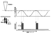
- the figure for demonstrating the relationship between the output timing of excitation light, and the distance between a probe and a sample (the 1).
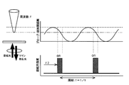
- the figure for demonstrating the relationship between the output timing of excitation light, and the distance between a probe and a sample (the 2).
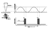
- the figure for demonstrating the relationship between the output timing of excitation light, and the distance between a probe and a sample (the 3).
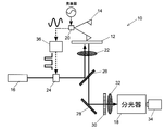
- FIG. 1 is a block diagram showing a schematic configuration of a signal light measurement system 10 (hereinafter referred to as system 10) of a near-field optical microscope according to an embodiment of the present invention.
- system 10 is a combination of a near-field optical microscope and a Raman spectroscope, and measures a Raman scattering spectrum observed by a near-field optical microscope using a probe to image a sample molecule.
- the system 10 includes a transparent substrate 12 such as a glass substrate on which a sample is placed, a probe 14 that scans the surface of the sample, an excitation light source 16 that irradiates the sample with excitation light, and a radiation emitted from the sample.
- the probe 14 is made of, for example, a silver tip having a silver thin film of about 35 nm deposited on the tip of a cantilever for an atomic force microscope.
- the cantilever is forcibly vibrated at a constant frequency in a direction perpendicular to the sample by a vibrator 20 such as a bimorph piezo element, whereby the tip of the silver chip is in intermittent contact with the sample surface. Further, when the silver chip comes into contact with the sample surface, the cantilever is automatically controlled so that the attenuation amount of the amplitude of the cantilever becomes constant.
- the sample is provided so as to be in contact with one surface of the transparent substrate 12, and a high aperture objective lens 22 is provided to face the other surface of the transparent substrate 12.
- the transparent substrate 12 is placed on a piezo movement stage (not shown) and is configured to be two-dimensionally scanable.
- the excitation light source 16 the beam splitter 26, the objective lens 22, and the transparent substrate 12 constitute a light irradiation mechanism.
- the Raman scattered light enters the spectroscope 18 through the transparent substrate 12, the objective lens 22, the beam splitter 26, the mirror 28, the excitation light removal filter 30, and the lens 32, and is detected by the nitrogen cooled CCD camera 34.
- the excitation light removal filter 30 is for removing excitation light that is much stronger than Raman scattered light, and generally a notch filter or an edge filter (long wavelength transmission filter) is used.
- the light modulator 24 includes, for example, an acousto-optic modulator (AOM) or an electro-optic modulator (EOM), and performs ON / OFF modulation of light emitted from the excitation light source 16 based on a modulation signal from the pulse generator 36.
- the pulse generator 36 outputs a pulse waveform having a predetermined pulse width synchronized with the vibration frequency of the cantilever as a modulation signal.
- FIGS. 2 to 4 are diagrams for explaining the relationship between the output timing of excitation light and the distance between the probe and the sample.
- the output timing of the modulation signal of the pulse generator 36 output timing of the excitation light
- the light is applied to the sample surface only when the distance between the probe and the sample is arbitrary. Is irradiated. For this reason, Raman scattered light can be detected when the distance between the probe and the sample is an arbitrary size.
- the probe-sample distance (Z) is expressed using the modulation signal output timing ( ⁇ ) as shown in the following equation (1). be able to.
- D is the maximum value of the probe-sample distance
- f is the probe vibration frequency
- ⁇ is the phase shift. Therefore, by changing the output timing of the modulation signal, it is possible to observe how the Raman scattered light changes depending on the probe-sample distance.
- Single-walled carbon nanotubes (SWNT) were used as samples.
- FIG. 6 shows the relationship between the G-band intensity of the Raman scattering spectrum and the output timing ⁇ ( ⁇ s). Further, FIG. 7 is obtained by converting the output timing on the horizontal axis of FIG.
- the Raman scattered light intensity is exponentially attenuated when the probe is separated from the sample.
- the attenuation distance was about 26.5 nm. This is considered to be due to the electromagnetic enhancement effect by the silver chip. That is, by measuring the signal light from the sample using the system 10, the probe-sample distance at which electromagnetic enhancement is observed, the probe-sample distance dependency of the electromagnetic enhancement effect, and the like can be examined. it can.
- FIGS. 8 (a) to 8 (c) show Raman scattering spectra when an adenine molecule aggregate is used as a sample using the system 10.
- FIG. FIG. 8 (a) is when the probe tip is sufficiently away from the adenine molecule (distance d to 200 nm)
- (b) is when the probe tip is in contact with the adenine molecule (distance d to 0.0 nm)
- (c) is It is a Raman scattering spectrum when the probe tip is pushed into the adenine molecule (distance d ⁇ 0.0 nm).
- 8A to 8C show smooth curves fitted with Lorentz curves together with experimental data (one in FIG. 8A, one in FIGS. 8B and 8C, respectively). Two fitting curves are shown).
- the optical modulator 24 is configured to turn on / off the excitation light in synchronization with the change in the distance between the probe tip and the sample.
- the switching timing for turning on / off the excitation light can be changed. Therefore, it is possible to measure only the signal light when the distance between the probe and the sample is an arbitrary size, and it is possible to observe the change in the signal light depending on the distance between the probe and the sample.
- the present invention is not limited to the above-described embodiment, and various modifications can be made without departing from the spirit of the present invention.
- the ON time of the modulation signal of the optical modulator 24 is shortened to reduce the pulse width of the optical pulse signal, the distance dependence can be measured with higher resolution.
- the vibration amplitude of the probe is reduced, it is possible to observe the spectral change in the close region where the distance between the probe and the sample is nanometer or less.
- the signal light when the distance between the probe and the sample is an arbitrary size can be measured, for example, in the fluorescence imaging of the metal tip enhanced type, the distance region (5) where the quenching of the fluorescence by the metal surface acts.
- the fluorescence signal can be continuously measured at a position farther than a nanometer).
- the vibration applying mechanism may apply vibration to both the probe and the sample, or may apply vibration only to the probe or only to the sample. In short, it is sufficient that the relative distance between the probe and the sample can be changed periodically.
- the probe is not limited to the scattering type, and may be an aperture type.
- the present invention can be applied to a system that detects various optical signals (Rayleigh scattering, Raman scattering, fluorescence, nonlinear optical signals, etc.) in a near-field optical microscope.
Abstract
Disclosed is a signal light measurement system for a near-field optical microscope which is capable of investigating the dependency of signal light emitted from a specimen by means of near-field light with respect to the distance between a probe and the specimen. This signal light measurement system is equipped with a probe (14) which scans the surface of a specimen, a light source (16), and a spectroscope (18) which detects signal light emitted from the specimen. The probe (14) comprising a cantilever and a silver chip on the tip thereof. The cantilever is vibrated by an oscillator (20), causing the tip of the silver chip to intermittently make contact with the surface of the specimen. Light emitted from the light source (16) passes through a light modulator (24), a beam splitter (26), an objective lens (22), and a transparent substrate (12), and strikes the specimen surface, generating near-field light at the specimen surface. Signal light is radiated from the specimen by means of this near-field light.
Description
本発明は、近接場光によって試料から放射される信号光を測定して当該試料のイメージングを行う近接場光学顕微鏡の信号光測定システムに関する。
The present invention relates to a signal light measurement system for a near-field optical microscope that measures signal light emitted from a sample by near-field light and images the sample.
走査型プローブ顕微鏡の一種である近接場光学顕微鏡は、光の回折限界を超えた空間分解能で顕微イメージングを実現できることから、産業上の実用化が進んでいる。近接場光学顕微鏡では、プローブの周りに発生させた近接場光で試料を照らし、プローブと試料表面との相互作用による散乱光の光強度や光学特性を計測することにより、試料の表面状態を検出する(例えば特許文献1参照)。
The near-field optical microscope, which is a kind of scanning probe microscope, has achieved practical industrial application because it can realize microscopic imaging with spatial resolution exceeding the diffraction limit of light. In the near-field optical microscope, the surface state of the sample is detected by illuminating the sample with near-field light generated around the probe and measuring the light intensity and optical characteristics of the scattered light due to the interaction between the probe and the sample surface. (See, for example, Patent Document 1).
プローブには開口型、散乱型があるが、いずれにおいてもプローブ先端と試料の距離に依存して計測される信号光(近接場光)の光強度や光学特性(分光特性)が変化する。これは、プローブと試料の間の化学的相互作用と電磁気学的な相互作用が介在するためである。従って、信号光のプローブ・試料間距離依存性を調べることができれば、プローブと試料との相互作用の解明が可能になる。
The probe has an aperture type and a scattering type. In either case, the light intensity and optical characteristics (spectral characteristics) of the signal light (near field light) measured depend on the distance between the probe tip and the sample. This is because chemical interaction and electromagnetic interaction between the probe and the sample are involved. Therefore, if the dependence of the signal light on the distance between the probe and the sample can be examined, the interaction between the probe and the sample can be clarified.
プローブ先端と試料との距離を制御する方式として、シアーフォース方式、走査型トンネル顕微鏡(STM)方式、原子間力顕微鏡(AFM)方式等がある。
いずれの方式も、プローブ先端と試料間を一定の距離に保つように制御するものであり、任意の距離における信号光を検出するものではない。 Methods for controlling the distance between the probe tip and the sample include a shear force method, a scanning tunneling microscope (STM) method, an atomic force microscope (AFM) method, and the like.
In either method, control is performed so as to maintain a constant distance between the probe tip and the sample, and signal light at an arbitrary distance is not detected.
本発明が解決しようとする課題は、近接場光により試料から放射される信号光のプローブ・試料間距離依存性を調べることができる近接場光学顕微鏡の信号光測定システムを提供することである。
The problem to be solved by the present invention is to provide a signal light measurement system of a near-field optical microscope capable of examining the probe-sample distance dependency of signal light emitted from a sample by near-field light.
上記課題を解決するために成された本発明は、先端が尖鋭なプローブを試料上で走査しつつ、前記プローブ近傍に生成される近接場光によって前記試料から放射される信号光を検出し当該試料のイメージングを行う近接場光学顕微鏡の信号光測定システムであって、
a) 前記プローブと試料との相対距離を周期的に変化させる振動付与機構と、
b) 前記プローブ近傍に近接場光を生成させるための光を照射する光照射機構と、
c) 前記プローブと前記試料との相対距離の変化に同期して、前記光照射機構が照射する光の強度を変化させる光強度変調機構と、
d) 前記試料から放射される信号光を測定する信号光測定機構と、
を備えることを特徴とする。 The present invention, which has been made to solve the above problems, detects signal light emitted from the sample by near-field light generated in the vicinity of the probe while scanning a probe with a sharp tip on the sample. A near-field optical microscope signal light measurement system for imaging a sample,
a) a vibration applying mechanism that periodically changes a relative distance between the probe and the sample;
b) a light irradiation mechanism for irradiating light for generating near-field light in the vicinity of the probe;
c) a light intensity modulation mechanism that changes the intensity of light emitted by the light irradiation mechanism in synchronization with a change in the relative distance between the probe and the sample;
d) a signal light measurement mechanism for measuring the signal light emitted from the sample;
It is characterized by providing.
この場合、光強度変調機構は、前記プローブと前記試料との相対距離の変化に同期して、前記光照射機構が照射する光をON/OFFすることが好ましい。
また、光強度変調機構は、ON/OFFの切換タイミングを変更可能に構成されていると良い。 In this case, it is preferable that the light intensity modulation mechanism turns ON / OFF the light irradiated by the light irradiation mechanism in synchronization with a change in the relative distance between the probe and the sample.
The light intensity modulation mechanism may be configured to be able to change the ON / OFF switching timing.
プローブと試料との相対距離を周期的に変化させることによりプローブと試料との間の化学的、電磁気学的な相互作用が変化し、これにより試料から放射される信号光の強度や分光特性が変化する。本発明では、プローブと試料との相対距離の周期的変化に同期して試料に照射される光強度が変化するため、得られる信号光の強度もプローブと試料との相対距離の周期的変化に同期して変化する。このため、例えば1周期分の信号光のうち最大値の信号光の強度や分光特性等を計測することにより、プローブ・試料間距離が任意の大きさのときの信号光の検出が可能になる。従って、プローブ・試料間距離に依存して信号光の強度や分光特性が変化する様子を観察することができる。
By periodically changing the relative distance between the probe and the sample, the chemical and electromagnetic interaction between the probe and the sample is changed, and the intensity and spectral characteristics of the signal light emitted from the sample are thereby changed. Change. In the present invention, the intensity of the light applied to the sample changes in synchronization with the periodic change in the relative distance between the probe and the sample, so that the intensity of the obtained signal light also changes with the periodic change in the relative distance between the probe and the sample. It changes synchronously. For this reason, for example, by measuring the intensity, spectral characteristics, etc. of the maximum value of the signal light for one period, it becomes possible to detect the signal light when the distance between the probe and the sample is an arbitrary size. . Accordingly, it is possible to observe how the intensity of the signal light and the spectral characteristics change depending on the distance between the probe and the sample.
次に、本発明の具体的な実施形態について図面を参照して説明する。
図1は本発明の一実施形態である近接場光学顕微鏡の信号光計測システム10(以下システム10という)の概略構成を示すブロック図である。このシステム10は、近接場光学顕微鏡とラマン分光器とを組み合わせたものであり、プローブを用いた近接場光学顕微鏡により観察されるラマン散乱スペクトルを測定し、試料分子のイメージングを行う。 Next, specific embodiments of the present invention will be described with reference to the drawings.
FIG. 1 is a block diagram showing a schematic configuration of a signal light measurement system 10 (hereinafter referred to as system 10) of a near-field optical microscope according to an embodiment of the present invention. Thissystem 10 is a combination of a near-field optical microscope and a Raman spectroscope, and measures a Raman scattering spectrum observed by a near-field optical microscope using a probe to image a sample molecule.
図1は本発明の一実施形態である近接場光学顕微鏡の信号光計測システム10(以下システム10という)の概略構成を示すブロック図である。このシステム10は、近接場光学顕微鏡とラマン分光器とを組み合わせたものであり、プローブを用いた近接場光学顕微鏡により観察されるラマン散乱スペクトルを測定し、試料分子のイメージングを行う。 Next, specific embodiments of the present invention will be described with reference to the drawings.
FIG. 1 is a block diagram showing a schematic configuration of a signal light measurement system 10 (hereinafter referred to as system 10) of a near-field optical microscope according to an embodiment of the present invention. This
具体的には、前記システム10は、試料が載置されるガラス基板などの透明基板12、前記試料の表面を走査するプローブ14、前記試料に励起光を照射する励起光源16、試料から放射される信号光としてのラマン散乱光を検出する分光器18を備えている。
前記プローブ14は、例えば原子間力顕微鏡用のカンチレバーの先端に約35nmの銀薄膜を蒸着した銀チップから成る。前記カンチレバーは、バイモルフピエゾ素子などの振動子20によって試料に垂直な方向に一定の振動数で強制振動されるようになっており、これにより銀チップの先端が試料表面に間欠接触する。また、銀チップが試料表面に接触した際、カンチレバーの振幅の減衰量が一定になるように、カンチレバーは自動制御される。 Specifically, thesystem 10 includes a transparent substrate 12 such as a glass substrate on which a sample is placed, a probe 14 that scans the surface of the sample, an excitation light source 16 that irradiates the sample with excitation light, and a radiation emitted from the sample. A spectroscope 18 for detecting Raman scattered light as signal light.
Theprobe 14 is made of, for example, a silver tip having a silver thin film of about 35 nm deposited on the tip of a cantilever for an atomic force microscope. The cantilever is forcibly vibrated at a constant frequency in a direction perpendicular to the sample by a vibrator 20 such as a bimorph piezo element, whereby the tip of the silver chip is in intermittent contact with the sample surface. Further, when the silver chip comes into contact with the sample surface, the cantilever is automatically controlled so that the attenuation amount of the amplitude of the cantilever becomes constant.
前記プローブ14は、例えば原子間力顕微鏡用のカンチレバーの先端に約35nmの銀薄膜を蒸着した銀チップから成る。前記カンチレバーは、バイモルフピエゾ素子などの振動子20によって試料に垂直な方向に一定の振動数で強制振動されるようになっており、これにより銀チップの先端が試料表面に間欠接触する。また、銀チップが試料表面に接触した際、カンチレバーの振幅の減衰量が一定になるように、カンチレバーは自動制御される。 Specifically, the
The
前記試料は透明基板12の一方の面に接するように設けられ、前記透明基板12の他方の面と対向して高開口の対物レンズ22が設けられている。なお、透明基板12は、図示しないピエゾ移動ステージに載置されており、2次元的に走査可能に構成されている。
前記励起光源16はHe-Cdレーザー(λ=441nm)等の単色光レーザー光源から成る。励起光源16から出射された励起光は、光変調器24、ビームスプリッタ26、対物レンズ22、透明基板12を経て、試料表面に照射される。励起光源16からの光は、高開口数の対物レンズ22により試料表面上に集光され、試料表面に近接場光を生成する。この近接場光と試料とが相互作用し、ラマン散乱光を生じる。従って、この実施の形態では、励起光源16、ビームスプリッタ26、対物レンズ22、透明基板12が光照射機構を構成する。
ラマン散乱光は、透明基板12、対物レンズ22、ビームスプリッタ26、ミラー28、励起光除去フィルタ30、レンズ32を経て分光器18に入射し、窒素冷却CCDカメラ34によって検出される。励起光除去フィルタ30はラマン散乱光に比べて非常に強い励起光を除去するためのもので、一般的にノッチフィルタもしくはエッジフィルタ(長波長透過フィルタ)が用いられる。 The sample is provided so as to be in contact with one surface of thetransparent substrate 12, and a high aperture objective lens 22 is provided to face the other surface of the transparent substrate 12. The transparent substrate 12 is placed on a piezo movement stage (not shown) and is configured to be two-dimensionally scanable.
Theexcitation light source 16 comprises a monochromatic laser light source such as a He—Cd laser (λ = 441 nm). Excitation light emitted from the excitation light source 16 is irradiated on the sample surface through the optical modulator 24, the beam splitter 26, the objective lens 22, and the transparent substrate 12. The light from the excitation light source 16 is condensed on the sample surface by the objective lens 22 having a high numerical aperture and generates near-field light on the sample surface. The near-field light and the sample interact to generate Raman scattered light. Therefore, in this embodiment, the excitation light source 16, the beam splitter 26, the objective lens 22, and the transparent substrate 12 constitute a light irradiation mechanism.
The Raman scattered light enters thespectroscope 18 through the transparent substrate 12, the objective lens 22, the beam splitter 26, the mirror 28, the excitation light removal filter 30, and the lens 32, and is detected by the nitrogen cooled CCD camera 34. The excitation light removal filter 30 is for removing excitation light that is much stronger than Raman scattered light, and generally a notch filter or an edge filter (long wavelength transmission filter) is used.
前記励起光源16はHe-Cdレーザー(λ=441nm)等の単色光レーザー光源から成る。励起光源16から出射された励起光は、光変調器24、ビームスプリッタ26、対物レンズ22、透明基板12を経て、試料表面に照射される。励起光源16からの光は、高開口数の対物レンズ22により試料表面上に集光され、試料表面に近接場光を生成する。この近接場光と試料とが相互作用し、ラマン散乱光を生じる。従って、この実施の形態では、励起光源16、ビームスプリッタ26、対物レンズ22、透明基板12が光照射機構を構成する。
ラマン散乱光は、透明基板12、対物レンズ22、ビームスプリッタ26、ミラー28、励起光除去フィルタ30、レンズ32を経て分光器18に入射し、窒素冷却CCDカメラ34によって検出される。励起光除去フィルタ30はラマン散乱光に比べて非常に強い励起光を除去するためのもので、一般的にノッチフィルタもしくはエッジフィルタ(長波長透過フィルタ)が用いられる。 The sample is provided so as to be in contact with one surface of the
The
The Raman scattered light enters the
前記光変調器24は例えば音響光学変調器(AOM)や電気光学変調器(EOM)から成り、パルスジェネレーター36からの変調信号に基づいて励起光源16から出射される光をON/OFF変調する。
前記パルスジェネレーター36は、カンチレバーの振動周波数に同期する所定のパルス幅のパルス波形を変調信号として出力するようになっている。また、パルスジェネレーター36は変調信号の出力タイミングを変更可能に構成されている。これにより、励起光源16からのレーザー光はカンチレバーの振動周波数に同期した任意のタイミングで光パルス信号に変換される。従って、この光パルス信号の周期Tはカンチレバーの振動周波数をfとするとT=1/fになる。 Thelight modulator 24 includes, for example, an acousto-optic modulator (AOM) or an electro-optic modulator (EOM), and performs ON / OFF modulation of light emitted from the excitation light source 16 based on a modulation signal from the pulse generator 36.
Thepulse generator 36 outputs a pulse waveform having a predetermined pulse width synchronized with the vibration frequency of the cantilever as a modulation signal. The pulse generator 36 is configured to change the output timing of the modulation signal. Thereby, the laser light from the excitation light source 16 is converted into an optical pulse signal at an arbitrary timing synchronized with the vibration frequency of the cantilever. Therefore, the period T of this optical pulse signal is T = 1 / f where f is the vibration frequency of the cantilever.
前記パルスジェネレーター36は、カンチレバーの振動周波数に同期する所定のパルス幅のパルス波形を変調信号として出力するようになっている。また、パルスジェネレーター36は変調信号の出力タイミングを変更可能に構成されている。これにより、励起光源16からのレーザー光はカンチレバーの振動周波数に同期した任意のタイミングで光パルス信号に変換される。従って、この光パルス信号の周期Tはカンチレバーの振動周波数をfとするとT=1/fになる。 The
The
図2~図4は、励起光の出力タイミングとプローブ・試料間距離との関係を説明するための図である。これらの図に示すように、パルスジェネレーター36の変調信号の出力タイミング(励起光の出力タイミング)をτ1~τ3に変化させることにより、任意のプローブ・試料間距離にあるときにのみ試料表面に光が照射される。このため、プローブ・試料間距離が任意の大きさのときにおけるラマン散乱光を検出できる。
FIGS. 2 to 4 are diagrams for explaining the relationship between the output timing of excitation light and the distance between the probe and the sample. As shown in these drawings, by changing the output timing of the modulation signal of the pulse generator 36 (output timing of the excitation light) to τ1 to τ3, the light is applied to the sample surface only when the distance between the probe and the sample is arbitrary. Is irradiated. For this reason, Raman scattered light can be detected when the distance between the probe and the sample is an arbitrary size.
カンチレバーは高さ方向に正弦関数で振動していると近似できることから、次の式(1)に示すように、プローブ・試料間距離(Z)は変調信号の出力タイミング(τ)を用いて表すことができる。

式(1)中、Dはプローブ・試料間距離の最大値、fはプローブの振動周波数、Φは位相ずれを示す。
従って、変調信号の出力タイミングを変化させることにより、プローブ・試料間距離に依存してラマン散乱光が変化する様子を観察することができる。 Since the cantilever can be approximated as oscillating with a sine function in the height direction, the probe-sample distance (Z) is expressed using the modulation signal output timing (τ) as shown in the following equation (1). be able to.
In Equation (1), D is the maximum value of the probe-sample distance, f is the probe vibration frequency, and Φ is the phase shift.
Therefore, by changing the output timing of the modulation signal, it is possible to observe how the Raman scattered light changes depending on the probe-sample distance.
従って、変調信号の出力タイミングを変化させることにより、プローブ・試料間距離に依存してラマン散乱光が変化する様子を観察することができる。 Since the cantilever can be approximated as oscillating with a sine function in the height direction, the probe-sample distance (Z) is expressed using the modulation signal output timing (τ) as shown in the following equation (1). be able to.
Therefore, by changing the output timing of the modulation signal, it is possible to observe how the Raman scattered light changes depending on the probe-sample distance.
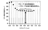
図5は、プローブの振動周波数fを123kHz(T=8.15μs)とし、変調信号のパルス幅を0.5μs、出力タイミング(τ)を0.5μs刻みで変化させたときに得られるラマン散乱スペクトルを示している。試料には、単層カーボンナノチューブ(SWNT)を用いた。図6は、ラマン散乱スペクトルのG-bandの強度と出力タイミングτ(μs)との関係を示している。さらに、図7は、図6の横軸の出力タイミングを数式1により距離に変換したものである。
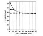
FIG. 5 shows a Raman scattering spectrum obtained when the vibration frequency f of the probe is 123 kHz (T = 8.15 μs), the pulse width of the modulation signal is changed by 0.5 μs, and the output timing (τ) is changed by 0.5 μs. ing. Single-walled carbon nanotubes (SWNT) were used as samples. FIG. 6 shows the relationship between the G-band intensity of the Raman scattering spectrum and the output timing τ (μs). Further, FIG. 7 is obtained by converting the output timing on the horizontal axis of FIG.
図7から明らかなように、ラマン散乱光強度はプローブが試料から離れると指数関数的に減衰している。そして、その減衰距離はおよそ26.5nmであった。これは、銀チップによる電磁気学的増強効果によるものと考えられる。つまり、上記システム10を用いて試料からの信号光を測定することにより、電磁気学的増強がみられるプローブ・試料間距離や電磁気学的増強効果のプローブ・試料間距離依存性等を調べることができる。
As is clear from FIG. 7, the Raman scattered light intensity is exponentially attenuated when the probe is separated from the sample. The attenuation distance was about 26.5 nm. This is considered to be due to the electromagnetic enhancement effect by the silver chip. That is, by measuring the signal light from the sample using the system 10, the probe-sample distance at which electromagnetic enhancement is observed, the probe-sample distance dependency of the electromagnetic enhancement effect, and the like can be examined. it can.
図8(a)~(c)は、上記システム10を用いて試料としてアデニン分子の凝集体を用いたときのラマン散乱スペクトルを示している。図8(a)はプローブ先端がアデニン分子から十分に離れているとき(距離d~200nm)、(b)はプローブ先端がアデニン分子に接触したとき(距離d~0.0nm)、(c)はプローブ先端がアデニン分子に押し込まれたとき(距離d<0.0nm)のラマン散乱スペクトルである。なお、図8(a)~(c)には、実験データと共にローレンツカーブでフィッティングした滑らかな曲線が示されている(図8の(a)では1本、(b)、(c)ではそれぞれ2本のフィッティング曲線が示されている)。
FIGS. 8 (a) to 8 (c) show Raman scattering spectra when an adenine molecule aggregate is used as a sample using the system 10. FIG. FIG. 8 (a) is when the probe tip is sufficiently away from the adenine molecule (distance d to 200 nm), (b) is when the probe tip is in contact with the adenine molecule (distance d to 0.0 nm), and (c) is It is a Raman scattering spectrum when the probe tip is pushed into the adenine molecule (distance d <0.0 nm). 8A to 8C show smooth curves fitted with Lorentz curves together with experimental data (one in FIG. 8A, one in FIGS. 8B and 8C, respectively). Two fitting curves are shown).
図8(a)に示すように、プローブ先端がアデニン分子から十分に離れているときは、プローブ先端の銀チップとアデニン分子との間に相互作用が介在しないため、通常の(つまり、銀チップがない状態で観察されるラマン散乱スペクトルと同様の)ラマン散乱スペクトルが観察される。従って、振動数721cm-1の通常のピーク(リングフリージングモードと呼ばれる振動モードによるピーク)が観察される。
As shown in FIG. 8 (a), when the probe tip is sufficiently away from the adenine molecule, no interaction is present between the silver tip at the probe tip and the adenine molecule. A Raman scattering spectrum is observed (similar to the Raman scattering spectrum observed in the absence). Therefore, a normal peak with a frequency of 721 cm −1 (a peak due to a vibration mode called a ring freezing mode) is observed.
これに対して、図8(b)に示すように、銀チップがアデニン分子に接触するときは、通常のピークに加えて、振動数731cm-1にシフトしたピークが観察される。このピークは、銀チップとアデニン分子との化学的相互作用(吸着)による増強と考えられた。
また、図8(c)に示すように、銀チップがアデニン分子を押し込んでいるときは、通常のピークに加えて736cm-1にシフトしたピークが観察される。これは、銀チップがアデニン分子を押圧することによる力学的作用が加わったためで、このとき、アデニン分子が歪んで分子振動の振動数が変化する。 In contrast, as shown in FIG. 8 (b), when the silver chip contacts the adenine molecule, a peak shifted to a frequency of 731 cm −1 is observed in addition to the normal peak. This peak was thought to be enhanced by chemical interaction (adsorption) between the silver chip and the adenine molecule.
In addition, as shown in FIG. 8 (c), when the silver chip pushes in the adenine molecule, a peak shifted to 736 cm −1 is observed in addition to the normal peak. This is because a mechanical action due to the silver chip pressing the adenine molecule is added. At this time, the adenine molecule is distorted and the frequency of molecular vibration is changed.
以上より、試料としてアデニン分子を用いたときは、プローブ・試料間距離が変化することによってラマン散乱光強度だけでなくスペクトル形状(ピーク)が変化することが分かる。これは、アデニン分子とプローブ先端との間に電磁気学的相互作用、化学的相互作用が生じているためであると考えられる。
これに対して、上述のカーボンナノチューブはプローブ先端との間で化学的相互作用が生じ難いため、カーボンナノチューブを試料として用いたときは、プローブ・試料間距離の変化によってラマン散乱光強度は変化したが、スペクトル形状はあまり変化しなかった。
従って、上記近接場光学顕微鏡システムを用いれば、化学的相互作用の起き易い分子の同定も可能となる。 From the above, it can be seen that when an adenine molecule is used as a sample, not only the Raman scattered light intensity but also the spectrum shape (peak) changes as the probe-sample distance changes. This is presumably because an electromagnetic interaction or a chemical interaction occurs between the adenine molecule and the probe tip.
On the other hand, since the above-mentioned carbon nanotube does not easily cause chemical interaction with the probe tip, when the carbon nanotube is used as a sample, the intensity of the Raman scattered light changes due to the change in the distance between the probe and the sample. However, the spectral shape did not change much.
Therefore, by using the near-field optical microscope system, it is possible to identify molecules that are likely to cause chemical interaction.
このように本実施の形態によれば、光変調器24はプローブ先端と試料間距離の変化に同期して励起光をON/OFFするように構成した。また、励起光をON/OFFする切換タイミングを変更可能に構成した。このため、プローブ・試料間距離が任意の大きさのときの信号光のみを測定することができ、プローブ・試料間距離に依存した信号光の変化を観察することができる。
Thus, according to the present embodiment, the optical modulator 24 is configured to turn on / off the excitation light in synchronization with the change in the distance between the probe tip and the sample. In addition, the switching timing for turning on / off the excitation light can be changed. Therefore, it is possible to measure only the signal light when the distance between the probe and the sample is an arbitrary size, and it is possible to observe the change in the signal light depending on the distance between the probe and the sample.
なお、本発明は、上記した実施の形態に限定されるものではなく、本発明の趣旨を逸脱しない範囲で種々の変更が可能である。
例えば、光変調器24の変調信号のON時間を短くして光パルス信号のパルス幅を小さくすれば、より高分解能で距離依存性を測定することができる。
また、プローブの振動振幅を小さくすれば、プローブ・試料間距離がナノメートル以下の近接領域でのスペクトル変化を観察することができる。
さらに、プローブ・試料間距離が任意の大きさのときの信号光を計測できるため、例えば金属チップ増強型の蛍光イメージングにおいては、金属表面による蛍光の消光(クエンチング)が作用する距離領域(5ナノメートル以下)よりも離れた位置で蛍光信号を計測し続けることができる。 The present invention is not limited to the above-described embodiment, and various modifications can be made without departing from the spirit of the present invention.
For example, if the ON time of the modulation signal of theoptical modulator 24 is shortened to reduce the pulse width of the optical pulse signal, the distance dependence can be measured with higher resolution.
Further, if the vibration amplitude of the probe is reduced, it is possible to observe the spectral change in the close region where the distance between the probe and the sample is nanometer or less.
Furthermore, since the signal light when the distance between the probe and the sample is an arbitrary size can be measured, for example, in the fluorescence imaging of the metal tip enhanced type, the distance region (5) where the quenching of the fluorescence by the metal surface acts. The fluorescence signal can be continuously measured at a position farther than a nanometer).
例えば、光変調器24の変調信号のON時間を短くして光パルス信号のパルス幅を小さくすれば、より高分解能で距離依存性を測定することができる。
また、プローブの振動振幅を小さくすれば、プローブ・試料間距離がナノメートル以下の近接領域でのスペクトル変化を観察することができる。
さらに、プローブ・試料間距離が任意の大きさのときの信号光を計測できるため、例えば金属チップ増強型の蛍光イメージングにおいては、金属表面による蛍光の消光(クエンチング)が作用する距離領域(5ナノメートル以下)よりも離れた位置で蛍光信号を計測し続けることができる。 The present invention is not limited to the above-described embodiment, and various modifications can be made without departing from the spirit of the present invention.
For example, if the ON time of the modulation signal of the
Further, if the vibration amplitude of the probe is reduced, it is possible to observe the spectral change in the close region where the distance between the probe and the sample is nanometer or less.
Furthermore, since the signal light when the distance between the probe and the sample is an arbitrary size can be measured, for example, in the fluorescence imaging of the metal tip enhanced type, the distance region (5) where the quenching of the fluorescence by the metal surface acts. The fluorescence signal can be continuously measured at a position farther than a nanometer).
プローブ増強型のラマン散乱イメージングにおいては、金属チップと分子が化学的に相互作用する瞬間のみの信号光を選択的に検出することができ、原子間力顕微鏡の空間分解能でラマンイメージングが実現できる。また、表面増強ラマン現象における分子と金属表面の吸着機構の解明にも大いに貢献できる。
In probe-enhanced Raman scattering imaging, it is possible to selectively detect signal light only at the moment when a metal tip and a molecule interact chemically, and to realize Raman imaging with the spatial resolution of an atomic force microscope. In addition, it can greatly contribute to the elucidation of the adsorption mechanism of molecules and metal surfaces in the surface enhanced Raman phenomenon.
振動付与機構は、プローブと試料の両方に振動を付与しても良く、プローブのみ、試料のみに振動を付与しても良い。要は、プローブと試料との相対距離を周期的に変化させることができれば良い。
プローブは散乱型に限らず、開口型でも良い。
本発明は、近接場光学顕微鏡において様々な光学信号(レーリー散乱、ラマン散乱、蛍光、非線形光学信号など)を検出するシステムに適用できる。 The vibration applying mechanism may apply vibration to both the probe and the sample, or may apply vibration only to the probe or only to the sample. In short, it is sufficient that the relative distance between the probe and the sample can be changed periodically.
The probe is not limited to the scattering type, and may be an aperture type.
The present invention can be applied to a system that detects various optical signals (Rayleigh scattering, Raman scattering, fluorescence, nonlinear optical signals, etc.) in a near-field optical microscope.
10…近接場光学顕微鏡の信号光計測システム
12…透明基板
14…プローブ
16…励起光源
18…分光器
20…振動子
24…光変調器 DESCRIPTION OFSYMBOLS 10 ... Signal light measuring system 12 of a near-field optical microscope ... Transparent substrate 14 ... Probe 16 ... Excitation light source 18 ... Spectroscope 20 ... Vibrator 24 ... Optical modulator
12…透明基板
14…プローブ
16…励起光源
18…分光器
20…振動子
24…光変調器 DESCRIPTION OF
Claims (4)
- 先端が尖鋭なプローブを試料上で走査しつつ、前記プローブ近傍に生成される近接場光によって前記試料から放射される信号光を検出し当該試料のイメージングを行う近接場光学顕微鏡の信号光測定システムにおいて、
a) 前記プローブと試料との相対距離を周期的に変化させる振動付与機構と、
b) 前記プローブ近傍に近接場光を生成させるための光を照射する光照射機構と、
c) 前記プローブと前記試料との相対距離の変化に同期して、前記光照射機構が照射する光の強度を変化させる光強度変調機構と、
d) 前記試料から放射される信号光を測定する信号光測定機構と、
を備えることを特徴とする近接場光学顕微鏡の信号光測定システム。 A signal light measurement system for a near-field optical microscope that detects signal light emitted from the sample by near-field light generated in the vicinity of the probe and scans the sample while scanning a probe having a sharp tip on the sample. In
a) a vibration applying mechanism that periodically changes a relative distance between the probe and the sample;
b) a light irradiation mechanism for irradiating light for generating near-field light in the vicinity of the probe;
c) a light intensity modulation mechanism that changes the intensity of light emitted by the light irradiation mechanism in synchronization with a change in the relative distance between the probe and the sample;
d) a signal light measurement mechanism for measuring the signal light emitted from the sample;
A signal light measurement system for a near-field optical microscope, comprising: - 光強度変調機構は、前記プローブと前記試料との相対距離の変化に同期して、前記光照射機構が照射する光をON/OFFすることを特徴とする請求項1に記載の近接場光学顕微鏡の信号光測定システム。 2. The near-field optical microscope according to claim 1, wherein the light intensity modulation mechanism turns on / off light emitted by the light irradiation mechanism in synchronization with a change in a relative distance between the probe and the sample. Signal light measurement system.
- 光強度変調機構は、ON/OFFの切換タイミングを変更可能に構成されていることを特徴とする請求項1に記載の近接場光学顕微鏡の信号光測定システム。 2. The signal light measurement system for a near-field optical microscope according to claim 1, wherein the light intensity modulation mechanism is configured to be capable of changing ON / OFF switching timing.
- 信号光は、レーリー散乱、ラマン散乱、蛍光、非線形光学信号の中から選択されるいずれかであることを特徴とする請求項1に記載の近接場光学顕微鏡の信号光測定システム。 2. The signal light measurement system for a near-field optical microscope according to claim 1, wherein the signal light is any one selected from Rayleigh scattering, Raman scattering, fluorescence, and nonlinear optical signal.
Applications Claiming Priority (2)
| Application Number | Priority Date | Filing Date | Title |
|---|---|---|---|
| JP2008-241151 | 2008-09-19 | ||
| JP2008241151A JP5270280B2 (en) | 2008-09-19 | 2008-09-19 | Signal light measurement system for near-field optical microscope |
Publications (1)
| Publication Number | Publication Date |
|---|---|
| WO2010032429A1 true WO2010032429A1 (en) | 2010-03-25 |
Family
ID=42039279
Family Applications (1)
| Application Number | Title | Priority Date | Filing Date |
|---|---|---|---|
| PCT/JP2009/004588 WO2010032429A1 (en) | 2008-09-19 | 2009-09-15 | Signal light measurement system for near-field optical microscope |
Country Status (2)
| Country | Link |
|---|---|
| JP (1) | JP5270280B2 (en) |
| WO (1) | WO2010032429A1 (en) |
Cited By (6)
| Publication number | Priority date | Publication date | Assignee | Title |
|---|---|---|---|---|
| JP2013544368A (en) * | 2010-11-29 | 2013-12-12 | ブルカー ナノ インコーポレイテッド | Method and apparatus for measuring physical properties of samples using peak forcing mode |
| US9207167B2 (en) | 2008-11-13 | 2015-12-08 | Bruker Nano, Inc. | Peak force photothermal-based detection of IR nanoabsorption |
| US9213047B2 (en) | 2008-11-13 | 2015-12-15 | Bruker Nano, Inc. | Method and apparatus of electrical property measurement using an AFM operating in peak force tapping mode |
| US9274139B2 (en) | 2008-11-13 | 2016-03-01 | Bruker Nano, Inc. | Method and apparatus of operating a scanning probe microscope |
| US9291640B2 (en) | 2008-11-13 | 2016-03-22 | Bruker Nano, Inc. | Method and apparatus of using peak force tapping mode to measure physical properties of a sample |
| US10845382B2 (en) | 2016-08-22 | 2020-11-24 | Bruker Nano, Inc. | Infrared characterization of a sample using oscillating mode |
Families Citing this family (4)
| Publication number | Priority date | Publication date | Assignee | Title |
|---|---|---|---|---|
| JP5802417B2 (en) | 2011-04-04 | 2015-10-28 | 株式会社日立製作所 | Scanning probe microscope and measuring method using the same |
| WO2013051094A1 (en) * | 2011-10-03 | 2013-04-11 | 株式会社日立製作所 | Scanning probe microscope |
| US9423416B2 (en) * | 2012-08-28 | 2016-08-23 | Hitachi, Ltd. | Scanning probe microscope and measuring method using same |
| FR3001294B1 (en) * | 2013-01-24 | 2015-03-20 | Ecole Polytech | MULTIMODE LOCAL PROBE MICROSCOPE, RAMAN EXTENDED RAMAN MICROSCOPE AND METHOD FOR CONTROLLING THE DISTANCE BETWEEN THE LOCAL PROBE AND THE SAMPLE |
Citations (2)
| Publication number | Priority date | Publication date | Assignee | Title |
|---|---|---|---|---|
| JPH07260808A (en) * | 1994-03-24 | 1995-10-13 | Seiko Instr Inc | Scanning near field interatomic force microscope |
| JP2002243618A (en) * | 2001-02-15 | 2002-08-28 | Seiko Instruments Inc | Method for measuring illumination reflection mode in scanning near-field microscope |
Family Cites Families (1)
| Publication number | Priority date | Publication date | Assignee | Title |
|---|---|---|---|---|
| AU2004227413B2 (en) * | 2003-04-04 | 2010-05-27 | Vp Holding, Llc | Method and apparatus for enhanced nano-spectroscopic scanning |
-
2008
- 2008-09-19 JP JP2008241151A patent/JP5270280B2/en active Active
-
2009
- 2009-09-15 WO PCT/JP2009/004588 patent/WO2010032429A1/en active Application Filing
Patent Citations (2)
| Publication number | Priority date | Publication date | Assignee | Title |
|---|---|---|---|---|
| JPH07260808A (en) * | 1994-03-24 | 1995-10-13 | Seiko Instr Inc | Scanning near field interatomic force microscope |
| JP2002243618A (en) * | 2001-02-15 | 2002-08-28 | Seiko Instruments Inc | Method for measuring illumination reflection mode in scanning near-field microscope |
Non-Patent Citations (2)
| Title |
|---|
| TAKA-AKI YANO ET AL.: "Confinement of enhanced field investigated by tip-sample gap regulation in tapping-mode tip-enhanced Raman microscopy", APPLIED PHYSICS LETTERS, vol. 91, 17 September 2007 (2007-09-17), pages 121101-1 - 121101-3 * |
| TARO ICHIMURA ET AL.: "Tip Zokyo Kinsetsuba Raman Spectrum no Tip -Shiryokan Kyori Izonsei no Sokuteiho", DAI 54 KAI EXTENDED ABSTRACTS, JAPAN SOCIETY OF APPLIED PHYSICS AND RELATED SOCIETIES, vol. 3, 27 March 2007 (2007-03-27), pages 1092 * |
Cited By (9)
| Publication number | Priority date | Publication date | Assignee | Title |
|---|---|---|---|---|
| US9207167B2 (en) | 2008-11-13 | 2015-12-08 | Bruker Nano, Inc. | Peak force photothermal-based detection of IR nanoabsorption |
| US9213047B2 (en) | 2008-11-13 | 2015-12-15 | Bruker Nano, Inc. | Method and apparatus of electrical property measurement using an AFM operating in peak force tapping mode |
| US9274139B2 (en) | 2008-11-13 | 2016-03-01 | Bruker Nano, Inc. | Method and apparatus of operating a scanning probe microscope |
| US9291640B2 (en) | 2008-11-13 | 2016-03-22 | Bruker Nano, Inc. | Method and apparatus of using peak force tapping mode to measure physical properties of a sample |
| US9322842B2 (en) | 2008-11-13 | 2016-04-26 | Bruker Nano, Inc. | Method and apparatus of operating a scanning probe microscope |
| US9810713B2 (en) | 2008-11-13 | 2017-11-07 | Bruker Nano, Inc. | Method and apparatus of operating a scanning probe microscope |
| US9995765B2 (en) | 2008-11-13 | 2018-06-12 | Bruker Nano, Inc. | Method and apparatus of using peak force tapping mode to measure physical properties of a sample |
| JP2013544368A (en) * | 2010-11-29 | 2013-12-12 | ブルカー ナノ インコーポレイテッド | Method and apparatus for measuring physical properties of samples using peak forcing mode |
| US10845382B2 (en) | 2016-08-22 | 2020-11-24 | Bruker Nano, Inc. | Infrared characterization of a sample using oscillating mode |
Also Published As
| Publication number | Publication date |
|---|---|
| JP2010071871A (en) | 2010-04-02 |
| JP5270280B2 (en) | 2013-08-21 |
Similar Documents
| Publication | Publication Date | Title |
|---|---|---|
| JP5270280B2 (en) | Signal light measurement system for near-field optical microscope | |
| US10845382B2 (en) | Infrared characterization of a sample using oscillating mode | |
| JP5311595B2 (en) | Microscope and observation method | |
| JP5828359B2 (en) | Mechanical detection of Raman resonance | |
| JP3425615B2 (en) | Scanning near-field atomic force microscope | |
| Accanto et al. | Phase control of femtosecond pulses on the nanoscale using second harmonic nanoparticles | |
| WO2014125729A1 (en) | Measuring device and measuring method | |
| WO2015079786A1 (en) | Light measuring device and light measuring method | |
| JP2008256672A (en) | Scanning probe microscope and method of observing sample using the same | |
| CN113056677A (en) | System for measuring absorption of laser emission by a sample | |
| JP2007278768A (en) | Microscope device | |
| Celebrano et al. | Hollow-pyramid based scanning near-field optical microscope coupled to femtosecond pulses: A tool for nonlinear optics at the nanoscale | |
| US8227767B2 (en) | Coherent nonlinear microscopy system and method with variation of the focal volume in order to probe the nanostructure of organized materials | |
| JP2009014547A (en) | Observation method for solid substance, grease evaluation method, and method for manufacturing bearing | |
| Vobornik et al. | Spectroscopic infrared scanning near-field optical microscopy (IR-SNOM) | |
| Furusawa et al. | Generation of broadband longitudinal fields for applications to ultrafast tip-enhanced near-field microscopy | |
| Tranca et al. | Nanoscale local modification of PMMA refractive index by tip-enhanced femtosecond pulsed laser irradiation | |
| Masaki et al. | Measurement of propagation of ultrafast surface plasmon polariton pulses using dual-probe scanning near-field optical microscopy | |
| CN110068554B (en) | Super-resolution microscope system for detecting small-size plasma nanoparticles | |
| Sobat et al. | An overview of scanning near-field optical microscopy in characterization of nano-materials | |
| Umakoshi et al. | Tip-Enhanced Raman Spectroscopy | |
| Celebrano et al. | Mapping local field enhancements at nanostructured metal surfaces by second‐harmonic generation induced in the near field | |
| Kolloch et al. | Characterization and applications of plasmon fields in metal nanostructures | |
| Wang et al. | Peak force infrared microscopy for label-free chemical imaging at sub 10 nm spatial resolution | |
| Bek | Apertureless SNOM: A new tool for nano-optics |
Legal Events
| Date | Code | Title | Description |
|---|---|---|---|
| 121 | Ep: the epo has been informed by wipo that ep was designated in this application |
Ref document number: 09814274 Country of ref document: EP Kind code of ref document: A1 |
|
| DPE1 | Request for preliminary examination filed after expiration of 19th month from priority date (pct application filed from 20040101) | ||
| NENP | Non-entry into the national phase |
Ref country code: DE |
|
| 122 | Ep: pct application non-entry in european phase |
Ref document number: 09814274 Country of ref document: EP Kind code of ref document: A1 |