WO2010026985A1 - 酸化スズ材料、表面処理された基板、表面処理された基板の製造方法、センサ用の電極およびセンサ - Google Patents
酸化スズ材料、表面処理された基板、表面処理された基板の製造方法、センサ用の電極およびセンサ Download PDFInfo
- Publication number
- WO2010026985A1 WO2010026985A1 PCT/JP2009/065328 JP2009065328W WO2010026985A1 WO 2010026985 A1 WO2010026985 A1 WO 2010026985A1 JP 2009065328 W JP2009065328 W JP 2009065328W WO 2010026985 A1 WO2010026985 A1 WO 2010026985A1
- Authority
- WO
- WIPO (PCT)
- Prior art keywords
- substrate
- tin
- treated
- tin oxide
- sensor
- Prior art date
- Legal status (The legal status is an assumption and is not a legal conclusion. Google has not performed a legal analysis and makes no representation as to the accuracy of the status listed.)
- Ceased
Links
Images






Classifications
-
- G—PHYSICS
- G01—MEASURING; TESTING
- G01N—INVESTIGATING OR ANALYSING MATERIALS BY DETERMINING THEIR CHEMICAL OR PHYSICAL PROPERTIES
- G01N27/00—Investigating or analysing materials by the use of electric, electrochemical, or magnetic means
- G01N27/02—Investigating or analysing materials by the use of electric, electrochemical, or magnetic means by investigating impedance
- G01N27/04—Investigating or analysing materials by the use of electric, electrochemical, or magnetic means by investigating impedance by investigating resistance
- G01N27/12—Investigating or analysing materials by the use of electric, electrochemical, or magnetic means by investigating impedance by investigating resistance of a solid body in dependence upon absorption of a fluid; of a solid body in dependence upon reaction with a fluid, for detecting components in the fluid
- G01N27/125—Composition of the body, e.g. the composition of its sensitive layer
- G01N27/127—Composition of the body, e.g. the composition of its sensitive layer comprising nanoparticles
-
- B—PERFORMING OPERATIONS; TRANSPORTING
- B82—NANOTECHNOLOGY
- B82Y—SPECIFIC USES OR APPLICATIONS OF NANOSTRUCTURES; MEASUREMENT OR ANALYSIS OF NANOSTRUCTURES; MANUFACTURE OR TREATMENT OF NANOSTRUCTURES
- B82Y15/00—Nanotechnology for interacting, sensing or actuating, e.g. quantum dots as markers in protein assays or molecular motors
-
- B—PERFORMING OPERATIONS; TRANSPORTING
- B82—NANOTECHNOLOGY
- B82Y—SPECIFIC USES OR APPLICATIONS OF NANOSTRUCTURES; MEASUREMENT OR ANALYSIS OF NANOSTRUCTURES; MANUFACTURE OR TREATMENT OF NANOSTRUCTURES
- B82Y30/00—Nanotechnology for materials or surface science, e.g. nanocomposites
Definitions
- the present invention relates to a tin oxide material, a surface-treated substrate, a method for producing such a surface-treated substrate, an electrode for a sensor, and a sensor having such an electrode.
- a general sensor electrode has a structure for quantitatively detecting a detection target substance by specifically adsorbing the detection target substance on the electrode surface and detecting a change in a small physical property value such as a current value generated thereby. .
- the sensitivity of the sensor greatly depends on the degree of adsorption of the detection target substance to the electrode surface.
- Non-Patent Document 1 when the electrode surface is modified with zinc oxide in order to increase the sensitivity of the sensor, the specific adsorptivity to the detection target substance is improved. Adsorption is also improved. Therefore, when such an electrode is used for a sensor, the signal-to-noise ratio (S / N ratio) of the sensor electrode is lowered due to undesired adsorption of a non-detection target substance, and the sensitivity of the sensor is lowered. there is a possibility.
- the entire electrode is affected by the electrical resistance of the porous film itself. As a result, there is a problem that an appropriate current cannot be detected when a detection target is detected.
- the present invention has been made in view of such a background, and a tin oxide material that can detect a proper current when used as a sensor electrode, has a high S / N ratio, and provides high sensitivity.
- An object of the present invention is to provide a treated substrate, a method for producing a surface-treated substrate, an electrode for a sensor, and a sensor.
- the surface of the tin oxide includes at least one of SnO and SnO 2 , and the surface exhibits nano-level unevenness due to the nanocrystals of tin oxide formed on the surface to be processed.
- a tin oxide material having an average crystal length of 3 nm to 50 nm is provided.
- a substrate and a tin oxide nanocrystal disposed on a surface of the substrate are provided, and the tin oxide nanocrystal is subjected to a surface treatment having an average length of 3 nm to 50 nm.
- a substrate is provided.
- an electrode for a sensor provided with the surface-treated substrate as described above.
- one sensor having the electrode as described above and selected from the group consisting of a molecular sensor, a DNA sensor, a solution sensor, and a gas sensor.
- a method for manufacturing a surface-treated substrate the step of preparing a substrate, the step of preparing a solution containing tin ions by adding a tin compound in a liquid, and the tin ions
- a method for producing a surface-treated substrate the method comprising the steps of immersing the substrate in a solution containing, and precipitating tin oxide nanocrystals on the treated surface of the substrate.
- an appropriate current when used as an electrode of a sensor, an appropriate current can be detected, a high S / N ratio, a high sensitivity, a tin oxide material, a surface-treated substrate, and a surface-treated substrate.
- a manufacturing method, an electrode for a sensor, and a sensor can be provided.
- the sensor electrode when increasing the sensitivity of a sensor, the sensor electrode (detection unit) has (i) a high specific adsorptivity to a substance to be detected, and (ii) a structure that increases reaction sites as much as possible. It is desirable to do.
- zinc oxide has a high specific adsorptivity with respect to a predetermined substance to be detected. Therefore, a material whose surface is modified with zinc oxide is used. It has been proposed.
- zinc oxide has a characteristic of having high adsorptivity not only for detection target substances but also for non-detection target substances. Therefore, when an electrode provided with a zinc oxide film on the surface is used for the sensor, both the detection target substance and the non-detection target substance are trapped by zinc oxide, thereby reducing the S / N ratio of the electrode, As a result, the sensitivity of the sensor may not be sufficiently increased.
- a porous coating film made of a material having specific adsorptivity is provided on the surface of the substrate material, and the surface area of the electrode is increased to increase the reaction site, thereby improving the sensitivity of the sensor. It is possible to make it.
- a porous coating film has a significantly increased electrical resistance, especially when it becomes thicker. Therefore, even if the substrate material is conductive, providing such a coating film increases the electrical resistance of the entire electrode. Such an increase in the electrical resistance of the electrode may lead to a decrease in the measurement efficiency of the sensor and a decrease in the sensitivity of the sensor.
- the tin oxide material according to an embodiment of the present invention has a structure in which a large number of tin oxide nanocrystals are formed on a surface of a substrate or the like. With such a structure, both the above-mentioned characteristics (i) and (ii) are satisfied. Therefore, when the material according to the present embodiment is used for, for example, an electrode of a sensor, an appropriate current can be detected, and the conventional technique is used. It is possible to obtain an electrode having significantly higher sensitivity than that of the electrode.
- the adsorptivity to the non-detection target substance is suppressed by using tin oxide instead of zinc oxide as the substance that captures the detection target substance.
- tin oxide tends to be slightly inferior in specific adsorption property to the detection target substance compared to zinc oxide, but it does not correspond to non-detection target substance compared to zinc oxide. It was confirmed that the adsorptivity was significantly lower than that of zinc oxide even when the specific adsorptivity to the detection target substance was somewhat inferior to that of zinc oxide.
- the tin oxide material of this example is formed on the surface of a substrate or the like in which a large number of nano level irregularities generated by the tin oxide nanocrystals are formed, and the surface has a large number of irregularities.
- the surface area can be increased by the amount.
- the nano level means a level of 0.1 nm to 1000 nm, and more narrowly means a level of 1 nm to 100 nm. Therefore, the above-mentioned characteristic (ii) is satisfied by the structure in which a large number of such nano-level irregularities are formed.
- the nano-bell unevenness on the surface of the substrate is not formed by providing a high electrical resistance material such as an oxide or a semiconductor material as a so-called “film”.
- the nano-level unevenness on the surface of the substrate is formed by dispersing nano-order crystals of tin oxide over the entire substrate surface. The whole is not covered.
- the nano order means the order of 0.1 nm to 1000 nm, and more narrowly means the order of 1 nm to 100 nm. Therefore, in this embodiment, the problem that the electrical resistance of the entire material increases due to the surface treatment can be significantly suppressed. Thereby, in a present Example, appropriate electric current detection is attained, the measurement efficiency is high, and the material for sensors which has high sensitivity can be provided.
- titanium oxide refers to a material containing one or both of SnO and SnO 2 .
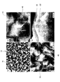
- FIG. 1 shows a SEM photograph of a tin oxide material according to an embodiment of the present invention.
- (a) to (c) are surface SEM photographs with different magnifications
- (d) is a cross-sectional SEM photograph of the electrode surface of the tin oxide material according to this example.
- the material according to the present embodiment includes the substrate 10 and a large number of tin oxide nanocrystals provided on the surface of the substrate 10 (hereinafter referred to as the substrate surface).
- the substrate surface is a portion composed of polygonal crystals 15 having relatively uniform dimensions throughout the entire photograph.
- the size of the polygonal crystal 15 is about 100 nm to 300 nm.
- the whitish thread-like substance that appears to be attached to the surface of the polygonal crystal 15 constituting the substrate surface is tin oxide.
- Nanocrystal 30 Although not clear from the direction of the photographs in FIGS. 1B and 1C, each of the tin oxide nanocrystals 30 has an elongated plate-like form, and its single length is 10 nm. About 30 nm.
- a large number of tin oxide nanocrystals 30 are formed on the surface of a polygonal crystal 15 constituting the substrate surface.
- a large number of extremely fine irregularities at the nano level are formed on the substrate surface, that is, the surface of the polygonal crystal 15 constituting the substrate surface.
- the nanocrystal 30 of tin oxide is not in the form of a general film, but is present as a large number of fine precipitates dispersed on the substrate surface.
- the material of this example can suppress a significant increase in electrical resistance and can significantly increase the surface area of the material surface.
- a plurality of strip-like precipitates 40 are formed on the substrate surface in addition to the tin oxide nanocrystal 30 shown in FIG. 1D.
- the strip-shaped precipitate 40 is made of tin oxide, and also looks like a plate when viewed from different directions. Therefore, hereinafter, this strip-like precipitate 40 will be referred to as a strip-sheet-like tin oxide crystal 40. Depending on the surface treatment conditions, the strip-shaped tin oxide crystal 40 may not be formed.
- tin oxide having a lower adsorptivity with respect to a non-detection target substance than zinc oxide is provided on the substrate surface in a nanocrystal state, thereby forming a large number of nano level unevenness on the substrate surface. be able to.
- the surface area of the material surface is significantly increased, and a significant increase in the electrical resistance of the material is suppressed.
- tin oxide nanocrystals can be grown directly on the substrate surface by nucleation. Therefore, in this embodiment, it is not necessary to interpose a third substance such as a seed layer or an intermediate layer between the substrate and the tin oxide nanocrystal.
- Such a tin oxide material according to the present embodiment can be used for electrodes (or detection units) of molecular sensors, DNA sensors, solution sensors, gas sensors and the like.
- the tin oxide material according to this example is used for the electrode of such a sensor, the surface area increases due to surface irregularities caused by the nanocrystals of tin oxide, and the low specific adsorption property of the tin oxide itself to non-detectable substances.
- a highly sensitive sensor with a high S / N ratio can be obtained.
- the tin oxide material according to this example can be used for gas sensors, dye-sensitized solar cells, filters, catalysts, and the like.
- the substrate on which the tin oxide nanocrystals are provided is not particularly limited, and may be a substrate of any material, form, or structure, or a surface to be processed.
- the substrate is made of a transparent material, but when used for other purposes such as a detection part of a gas sensor, the substrate is made of an opaque material. It may be configured.
- the substrate (or the surface to be processed) may be made of a conductive material or a non-conductive material.
- the material of the substrate may be glass, FTO (fluorine-doped tin oxide), silicon, indium tin oxide (ITO), or the like.
- the material of the substrate may be a heat-sensitive material such as a polymer film, paper, or rubber. Note that, when the material of the substrate contains tin oxide, both the nanocrystal and the substrate contain tin oxide, so that the adhesion of the nanocrystal to the substrate can be further improved.
- the shape of the substrate may be a flat shape, a particle shape, a fiber shape, or the like, or another complicated shape.
- the surface state of the substrate is not particularly limited.
- the substrate surface may be hydrophilic or hydrophobic, for example.
- the size of the tin oxide nanocrystal 30 is not particularly limited.
- the average length of the tin oxide nanocrystals 30 may be, for example, in the range of about 1 nm to 100 nm.
- the average length of the strip-shaped tin oxide crystals 40 is not particularly limited.
- the average length of the strip-shaped tin oxide crystals 40 may be, for example, in the range of about 10 nm to 1000 nm.
- the “average length” of the tin oxide nanocrystals 30 was determined as an average of 10 points of typical lengths of the tin oxide nanocrystals 30 in the SEM photograph.
- the “average length” of the strip-sheet-shaped tin oxide crystals 40 was determined as an average of 10 points of the length of the strip-sheet-shaped tin oxide crystals 40 having typical dimensions in the SEM photograph.
- FIG. 2 is a flowchart showing a method of forming a tin oxide material according to an embodiment of the present invention, that is, a method of manufacturing a surface-treated substrate in the present embodiment.
- a substrate for providing a tin oxide nanocrystal is prepared.
- the substrate is not particularly limited, and may be any material, form, or structure.
- the substrate surface is cleaned by washing with an organic solvent such as acetone or ethanol, ultraviolet irradiation or the like.
- the substrate may be masked with a masking tape or the like except for the surface treatment region.
- a solution for depositing tin oxide nanocrystals on the substrate prepared in step S110 is prepared.
- the solution is preferably an aqueous solution from the viewpoint of ease of handling, but may be a non-aqueous solvent such as an organic solvent as long as tin oxide is precipitated.
- the solution may use a hydrothermal reaction.
- the solution is an aqueous solution
- a tin compound is added to the aqueous solution to prepare a solution containing tin ions.
- the tin compound may contain any valent tin, and the tin may be divalent or tetravalent.
- Examples of the tin compound include SnF 4 (tin fluoride), SnCl 4 (tin tetrachloride), SnCl 2 (tin dichloride), SnCl 2 ⁇ 2H 2 O (tin chloride dihydrate), SnCl 4 ⁇ 5H 2.
- the tin compound is SnF 4 (tin fluoride), SnCl 4 (tin tetrachloride), SnCl 2 (tin dichloride), SnCl 2 .2H 2 O (tin chloride dihydrate), SnCl 4.
- the concentration of tin ions contained in the solution is not particularly limited.
- the concentration of tin ions may be in the range of 0.1 mM to 100 mM, for example. If the concentration of tin ions is higher than 100 mM, the time for the precipitation reaction is significantly shortened, so that the control becomes relatively difficult. Further, when the tin ion concentration is less than 0.1 mM, the time for the precipitation reaction is significantly increased. However, even if the concentration of tin ions is outside the range of 0.1 mM to 100 mM, there is no significant change in the properties of the resulting tin oxide nanocrystals. Therefore, the concentration of tin ions outside the range of 0.1 mM to 100 mM. May be adopted.
- step S130 the substrate prepared in step S110 is immersed in the solution prepared in step S120 in the container (or chamber) 101, and tin oxide nanocrystals are deposited and grown on the substrate.
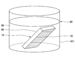
- FIG. 3 schematically shows a state in which the substrate 10 is immersed in a solution 60 containing tin ions.
- the substrate 10 has a surface-treated surface 70 that is surface-treated with tin oxide and a non-treated surface 80 on the opposite side.
- the substrate 10 when the substrate 10 is immersed in the solution 60 in the container 101, it is preferable to immerse the substrate 10 in such a direction that the surface to be treated 70 of the substrate 10 is “downward”.
- the surface-treated surface 70 of the substrate 10 is set to “upward”, tin oxide floating in the solution after deposition stays on the surface-treated surface 70 of the substrate 10 and hinders subsequent deposition and growth of tin oxide. Because there is a fear.
- “downward” means that the surface to be processed 70 of the substrate 10 is parallel to the liquid surface 90 of the solution 60 and is downward, as shown in FIG. Is inclined at an angle other than 90 ° with respect to the liquid surface 90 of the solution 60 and includes a downward state.
- the floating tin oxide does not stay on the surface-treated surface 70 and falls toward the bottom of the solution 60 to form a precipitate.
- the temperature of the solution and the treatment time during the treatment are not particularly limited, but when the temperature is low, it is necessary to hold the substrate for a longer time.
- the treatment temperature can be set, for example, in the range of room temperature to 99 ° C., for example, 90 ° C.
- the processing time is not particularly limited, but can be set in the range of 1 minute to 24 hours, for example, 20 minutes.
- the substrate is taken out of the solution and washed with water. Thereafter, when the masking process is performed, the masking material is removed.
- the substrate 10 on which the tin oxide nanocrystals are deposited can be obtained.
- the size of the tin oxide nanocrystal varies depending on the processing conditions, and is, for example, about 1 nm to 100 nm. Further, as described above, the size (full length) of the strip-like tin oxide crystals that can exist simultaneously with the tin oxide nanocrystals varies depending on the processing conditions, but is, for example, about 10 nm to 300 nm.
- high temperature treatment is not required for the formation or expression of tin oxide nanocrystals. Accordingly, the degree of freedom of selection of the substrate material is widened, and a material that is weak against heat can be used for the substrate.
- Example 1 Specific examples of steps S110, S120, and S130 will be described below.
- an FTO substrate (length 26 mm ⁇ width 50 mm ⁇ thickness 1.1 mm, 9.3-9.7 ⁇ / ⁇ , manufactured by Asahi Glass Co., Ltd.) is irradiated with ultraviolet rays (UV). It was.
- the main wavelengths of light from this light source were 184.9 nm and 253.7 nm, and the irradiation time was 10 minutes.
- the contact angle of the FTO substrate surface changes (decreases) depending on the UV irradiation time.
- the FTO substrate surface in the initial state has a contact angle with water of 96 ° and is a hydrophobic surface, whereas the contact angle became 70 ° by UV irradiation for 30 seconds.
- the contact angles changed to 54 °, 30 °, 14 °, and 5 ° by UV irradiation for 1, 2, 3, and 4 minutes, respectively. With UV irradiation for 5 minutes or more, the contact angle on the FTO surface showed superhydrophilicity of almost 0 ° below the measurement limit.
- a masking tape was installed in the surface treatment area of the FTO substrate, and a masking process was performed.
- a masking process was performed out of the surface of the FTO substrate that has been subjected to UV irradiation, from the respective sides of the width of the FTO substrate to the region 14 mm inward, and the surface side that has not been subjected to UV irradiation are treated as non-surface-treated regions (that is, Masking region).
- step S120 a solution for surface treatment was prepared.
- the solution was prepared by adding SnF 2 (mass number 156.71 g, purity 90.0%, manufactured by Wako Pure Chemical Industries, Ltd.) to distilled water at a concentration of 5 mM.
- step S130 the FTO substrate masked as described above was completely immersed in the solution so as to have an inclination of about 45 ° with respect to the solution surface. At this time, the FTO substrate was completely immersed in the solution so that the surface treatment region was on the lower side.
- the temperature of the solution was 90 ° C. and the immersion time was 20 minutes.
- the FTO substrate was taken out of the solution and washed with running water.
- the adhesion between the FTO substrate and the tin oxide nanocrystals was extremely good, and the nanocrystals did not fall off even in the treatment with running water.
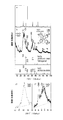
- FIG. 4 is a view showing an X-ray diffraction result of a tin oxide material according to an embodiment of the present invention.
- the vertical axis represents intensity (arbitrary unit), and the horizontal axis represents 2 ⁇ (°) (CuK ⁇ ).
- CuK ⁇ represents that measurement was performed using Cu (copper) as a target of the X-ray generation source and using the K ⁇ ray.
- RINT-2100V manufactured by Rigaku Corporation was used as the measuring device. The measurement result is indicated by a in FIG.
- the particles that do not adhere to the FTO substrate 10 and fall off and precipitate in the solution are collected by a centrifugal separator (model 8920, manufactured by Kubota Corporation). Then, XRD measurement was performed again. The rotation speed of the centrifuge was 4000 rpm, and the centrifugation time was 10 minutes.
- FIG. 4 b shows the measurement result of the particles thus recovered.
- the diffraction peak of SnO 2 was broader than the diffraction peak of SnO, that is, it was gentler. From this, it is considered that the SnO 2 precipitate has a smaller crystallite size and lower crystallinity than the SnO precipitate.
- the crystal size d is expressed as follows using the diffraction angle ⁇ , the wavelength ⁇ (1.54051 ⁇ ) of the incident X-ray, and the half-value width ⁇ (Scherrer equation).
- d k ⁇ / ⁇ cos ⁇ Formula (1)
- k is 0.9.
- the SnO 2 (211) ratio of the intensity of the SnO (200) diffraction peak to diffraction peak was 0.537.
- the ratio of integrated intensity of the SnO (200) diffraction peak to the SnO 2 (211) diffraction peak was 4.65.
- the ratio of the intensity intensity of the diffraction peak and the ratio of the integrated intensity correlate with the abundance of the substance, and these results indicate that the sample contains more SnO 2 than SnO.
- FIG. 1 corresponds to a SEM photograph of the surface of the surface treated FTO substrate 10 obtained as described above.
- FIG. 1 (a) to (c) are surface SEM photographs with different magnifications, and (d) is a cross-sectional SEM photograph.
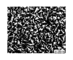
- FIG. 5 shows a surface SEM photograph of an FTO substrate not subjected to surface treatment for comparison.
- FIG. 1 (a) to 1 (d) it was confirmed that tin oxide nanocrystals were uniformly formed on the surface of the FTO substrate 10.
- FIG. 1 (d) it was confirmed that the surface of the FTO substrate 10 was formed with irregularities of about 5 nm to 10 nm by tin oxide nanocrystals.
- strip sheet-like tin oxide crystals were dispersed on the entire surface of the FTO substrate 10.
- the strip-shaped tin oxide crystals had a width of 10 nm to 20 nm, a length of 100 nm, a thickness of about 5 nm, and an aspect ratio of about 5 to 10.
- FIG. 6 shows a TEM photograph of a cross section along a direction perpendicular to the surface of the surface-treated FTO substrate 10.
- the FTO substrate 10 looks black.
- a flat surface and a polycrystalline surface having a sharp angle are mixed.
- nanocrystals 30 of tin oxide having a nano-order dimension were observed on the surface of the FTO substrate 10.
- the tin oxide nanocrystal 30 was about 10 nm in size and rounded.
- a lattice image was observed in a part of the tin oxide nanocrystal 30, and the lattice spacing was about 0.33 nm to 0.37 nm.
- the lattice spacing of the tin oxide nanocrystal 30 coincided with the lattice spacing of the (110) plane of SnO 2 .
- the region that was surface-treated with tin oxide showed the same color and gloss as the region that was not surface-treated, and the boundary between the two regions was unclear. From this, it was confirmed that the surface treatment of tin oxide according to the present example can be performed without changing the color of the substrate.
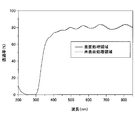
- FIG. 7 shows UV-Vis spectra of both surface regions of the surface-treated FTO substrate (surface-treated FTO substrate) 10 and the surface-treated FTO substrate (unsurface-treated FTO substrate).
- the vertical axis indicates the transmittance (%)
- the horizontal axis indicates the wavelength (nm)
- the solid line indicates the result in the surface-treated region with tin oxide
- the broken line indicates the result in the non-surface-treated region. Indicates. From FIG.
- the transmission characteristics of both surface regions of the surface-treated FTO substrate and the non-surface-treated FTO substrate are almost the same, and the transmittance of the FTO substrate 10 hardly decreases even when the surface treatment is performed with tin oxide.
- the size of the tin oxide nanocrystals 30 deposited by the surface treatment was a size equal to or smaller than the visible light wavelength (that is, 300 nm or less).
- a device is driven by light excitation, and thus a high visible light transmittance is required for an electrode. From the result of FIG. 7, it was confirmed that the material formed according to this example can be used for such a device that requires high visible light transmittance.
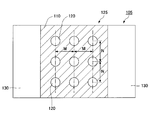
- FIG. 8 is a schematic top view of the FTO substrate 105 in which a tape having nine holes is arranged on the surface treatment region.
- the FTO substrate 105 corresponds to the FTO substrate 10 and has a center-side surface treatment region 125 and both end surface non-surface treatment regions 130.
- the tape 110 arranged on the surface-treated region 125 has nine holes 120.
- the pitch N of each step is 5 mm.
- the diameter of each hole is 3 mm.
- M is the pitch in the horizontal direction of the holes 120
- N is the pitch in the vertical direction of the holes 120.
- ssDNA-Cy5 (cy5-DP53-t: Cy5-GCGGCATGAACCTGAGGCCCCATCCT), which is a dye-labeled DNA, was dissolved in water to prepare solutions with dye concentrations of 1 ⁇ M and 100 nM (hereinafter referred to as solutions A and B, respectively). Called). Further, ssDNA (lamda-gt10: TTGAGCAAGTTCAGCCCTGGTTAAG), which is DNA not containing a dye, was dissolved in water to prepare a solution having a DNA concentration of 1 ⁇ M (hereinafter referred to as C solution).
- the FTO substrate 105 was air-dried at 95 ° C. for 10 minutes, rinsed three times for 15 minutes each using a sodium dodecyl sulfate (SDS, NaC 12 H 25 SO 4 ) solution, and then further added to ultrapure water. Rinse three times. Thereafter, the FTO substrate 105 was boiled in pure water for 2 minutes, immersed in absolute ethanol at 4 ° C. for 1 minute, and then dried by air blow.
- SDS sodium dodecyl sulfate
- the FTO105 substrate thus obtained was irradiated with a He / Ne laser with excitation light of 633 nm (Tyhuntrio scanner, GE Healthcare UK), and the fluorescence characteristics from each hole 120 were evaluated.
- Table 1 shows the intensity of fluorescence obtained from the FTO substrate 105.
- Table 1 simultaneously shows the results obtained with an unsurface-treated FTO substrate for comparison.
- the rightmost column shows the ratio of the fluorescence intensity of the surface-treated FTO substrate 105 to the fluorescence intensity of the unsurface-treated FTO substrate. From the results shown in Table 1, 16 times the intensity of fluorescence is detected from the surface-treated FTO substrate 105 that has been dye-adsorbed with the liquid A, compared to the non-surface-treated FTO substrate that has been subjected to the same dye adsorption. It was confirmed.
- photocurrent was evaluated by the following method using the surface-treated FTO substrate 105 obtained as described above.
- the surface-treated FTO substrate 105 was irradiated with red laser excitation light (wavelength 632 nm) with an output power of 0.7 mW or red laser excitation light (wavelength 650 nm) with an output power of 97 mW, and the resulting photocurrent value was measured. .
- Table 2 shows the measurement results of such photocurrent values.
- IPCE indicates the photoelectric conversion efficiency calculated from the following equation.
- IPCE (%) 1250I sc ( ⁇ A / cm 2) / ⁇ (nm) / P in (W / m 2 ) ⁇ 100
- I sc is the current density
- lambda is the wavelength
- P in the excitation light irradiation intensity is reported, for example, in Non-Patent Document 2.
- the ratio of the photocurrent value obtained with the A liquid to the photocurrent value obtained with the C liquid that is, the signal-to-noise ratio was shown. From Table 2, it is confirmed that the signal-to-noise ratio is 14 under the irradiation of the laser with the output power of 0.7 mW, and the signal-to-noise ratio is 29 under the irradiation of the laser with the output power of 97 mW. It was.
- the signal-to-noise ratio was sufficiently large, and it was confirmed that the material of this example can be used as an electrode for a high-sensitivity sensor.
- Example 2 Next, as another example of the present invention, a surface-treated FTO substrate was produced in the same manner as in the above example. However, in this example, the surface treatment was performed by changing the immersion time of the FTO substrate in the solution.
- 9 and 10 show surface SEM photographs of the FTO substrate surface-treated with different immersion times in the solution.
- 9, (a) and (b) show the FTO substrate surface-treated with an immersion time of 5 minutes
- (c) and (d) in FIG. 9 were surface-treated with an immersion time of 10 minutes.
- 9 shows an FTO substrate
- (e) and (f) in FIG. 9 show the FTO substrate surface-treated with a dipping time of 20 minutes as in the above example.
- (a) and (b) in FIG. 10 show the FTO substrate surface-treated with an immersion time of 30 minutes
- (c) and (d) in FIG. 10 are surface-treated with an immersion time of 1 hour.
- 10 (e) and 10 (f) show FTO substrates that have been surface-treated with an immersion time of 2 hours.
- the average length of the tin oxide nanocrystals tends to increase as the immersion time of the FTO substrate in the solution increases. That is, the immersion time of the FTO substrate in the solution increased to 5 minutes, 10 minutes, 20 minutes, 30 minutes, 1 hour and 2 hours, and the average lengths of the tin oxide nanocrystals on the surface of the FTO substrate were 3 nm and 5 nm, respectively. Growing to 10 nm, 20 nm, 50 nm and 100 nm. In addition, the average length of the strip-like tin oxide crystals increased, and the average length grew to about 100 nm to 150 nm when the immersion time was 1 hour. In addition, when immersion time was 5 minutes or less, the expression of the strip sheet-like tin oxide crystal was not confirmed.
- FIG. 11 shows the relationship between the average length of tin oxide nanocrystals deposited on the surface-treated FTO substrate and the fluorescence intensity when the liquid A and liquid B were dropped.
- the vertical axis indicates the fluorescence intensity (arbitrary unit), and the horizontal axis indicates the nanocrystal average length (nm).
- the fluorescence intensity was hardly obtained in the experiment in which the liquid C was dropped, the experimental result in that case is not shown in FIG. Regardless of the dye concentration in the solution, it was confirmed that the fluorescence intensity increased as the average length of the nanocrystals increased.
- FIG. 11 show that as the average length of the nanocrystals increases, fine irregularities on the surface of the FTO substrate become prominent, and the surface area of the FTO substrate increases, so that the amount of dye adsorbed on the FTO substrate increases. It shows that the fluorescence intensity is improved.
- the photocurrent value is the surface treatment FTO substrate in which the average length of the tin oxide nanocrystal is 10 nm (immersion time 20 minutes). The maximum value was shown (namely, the measured value in A liquid).
- the fluorescence intensity increased as the average length of the tin oxide nanocrystals increased.
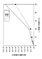
- the measurement result of the photocurrent value did not agree with this tendency, and as shown in FIGS. 12 and 13, the maximum value was shown when the average length of the tin oxide nanocrystals was 10 nm. This indicates that the photocurrent is not only dependent on the amount of dye adsorbed on the surface-treated FTO substrate, but also greatly influenced by the conductivity of the surface-treated FTO substrate.
- the material of this example is used for an electrode of a sensor such as a molecular sensor, it is considered most effective to provide tin oxide having an average nanocrystal length of about 10 nm.
- the average length of the nanocrystal is 10 nm. It was confirmed that a surface-treated substrate provided with tin oxide nanocrystals having an average nanocrystal length of 3 nm to 50 nm can be sufficiently used as a sensor electrode.
- the strip-sheet-like tin oxide crystals can be synthesized, and the strip-sheet-like tin oxide crystals in such a range are provided. Since a desired performance as a sensor electrode is expected with a surface-treated substrate, it can be used sufficiently as a sensor electrode.
- the tin oxide material according to the present invention can be used, for example, for electrodes of molecular sensors, DNA sensors, solution sensors, gas sensors and the like.
- the tin oxide material according to the present invention can also be used for electrodes, filters, catalysts and the like of dye-sensitized solar cells.
Landscapes
- Chemical & Material Sciences (AREA)
- Engineering & Computer Science (AREA)
- Nanotechnology (AREA)
- Life Sciences & Earth Sciences (AREA)
- Health & Medical Sciences (AREA)
- General Physics & Mathematics (AREA)
- General Health & Medical Sciences (AREA)
- Crystallography & Structural Chemistry (AREA)
- Physics & Mathematics (AREA)
- Molecular Biology (AREA)
- Composite Materials (AREA)
- Materials Engineering (AREA)
- Condensed Matter Physics & Semiconductors (AREA)
- Chemical Kinetics & Catalysis (AREA)
- Electrochemistry (AREA)
- Analytical Chemistry (AREA)
- Biochemistry (AREA)
- Immunology (AREA)
- Pathology (AREA)
- Other Surface Treatments For Metallic Materials (AREA)
- Investigating Or Analyzing Materials By The Use Of Fluid Adsorption Or Reactions (AREA)
Abstract
例えばセンサの電極として使用可能な酸化スズ材料は、SnOとSnO2の少なくとも一方を含み、被処理表面上に形成された状態で表面が酸化スズのナノ結晶によりナノレベルの凹凸を発現し、前記酸化スズのナノ結晶の平均長さは3nm~50nmである。
Description
本発明は、酸化スズ材料、表面処理された基板、そのような表面処理された基板の製造方法、センサ用の電極、およびそのような電極を有するセンサに関する。
ダイオキシンやビスフェノールAを検知する分子センサ、DNAセンサ、溶液センサ等の各種センサにおいては、検出対象に対して高い感度を示す電極(または検出部)の開発が求められている。
一般のセンサ電極は、検出対象物質を電極表面に特異吸着させ、これにより生じる電流値などの微小な物性値の変化を検出することにより、検出対象物質を定量的に検出する構造となっている。このため、センサの感度は、この検出対象物質の電極表面への吸着の度合いに大きく依存する。
一方、従来より、酸化亜鉛は、特定の物質に対して良好な特異吸着性を示すことが知られている。また、電極表面を酸化亜鉛で表面処理することにより、センサの感度を向上させる技術が報告されている(非特許文献1)。
Matt Law et al,, NatureMaterials, vol.4, "Nanowire dye-sensitized solar cells", June 2005年
M. K. Nazeeruddin et al., "Conversionof Light to Electricity by cis-X2Bis(2,2'-bipyridyl-4,4'-dicarboxylate)ruthenium(II) Charge-Transfer Sensitizers (X=Cl-, Br-, I-,CN-, and SCN-) on Nanocrystalline TiO2Electrodes", M. Journal of the American Chemical Society, 115,pp.6382-6390, 1993
しかしながら、前述の非特許文献1のように、センサの高感度化を図るため、電極表面を酸化亜鉛で改質した場合、検出対象物質に対する特異吸着性は向上するものの、同時に非検出対象物質の吸着性も向上してしまう。従って、そのような電極をセンサに使用した場合、好ましくない非検出対象物質の吸着により、センサ電極の信号対ノイズ比(S/N比)が低下してしまい、センサの感度が低下してしまう可能性がある。
また、センサの感度を高めるため、例えば、前述のような酸化亜鉛の多孔質膜を表面に設けることにより、センサ電極の表面積を大きくしようとすると、多孔質膜自身の電気抵抗の影響で電極全体の電気抵抗が増大し、検出対象の検出時に適正な電流検出ができなくなってしまうという問題が生じる。
本発明は、このような背景に鑑みなされたものであり、センサの電極として使用した際に適正な電流検出が可能であり、S/N比が高く、高い感度が得られる酸化スズ材料、表面処理された基板、表面処理された基板の製造方法、センサ用の電極およびセンサを提供することを目的とする。
本発明の一観点によれば、SnOとSnO2の少なくとも一方を含み、被処理表面上に形成された状態で表面が酸化スズのナノ結晶によりナノレベルの凹凸を発現し、前記酸化スズのナノ結晶の平均長さは3nm~50nmである酸化スズ材料が提供される。
本発明の一観点によれば、基板と、該基板の表面に設置けられた酸化スズのナノ結晶を有し、前記酸化スズのナノ結晶は、3nm~50nmの平均長さを有する表面処理された基板が提供される。
本発明の一観点によれば、上記の如き表面処理された基板を備えるセンサ用の電極が提供される。
本発明の一観点によれば、上記の如き電極を有し、分子センサ、DNAセンサ、溶液センサおよびガスセンサからなる群から選定された1つのセンサが提供される。
本発明の一観点によれば、表面処理された基板の製造方法であって、基板を準備するステップと、液体中にスズ化合物を添加して、スズイオンを含む溶液を調製するステップと、前記スズイオンを含む溶液中に前記基板を浸漬し、前記基板の処理表面に酸化スズのナノ結晶を析出させるステップを有する表面処理された基板の製造方法が提供される。
本発明では、センサの電極として使用した際に、適正な電流検出が可能であり、S/N比が高く、高い感度が得られる酸化スズ材料、表面処理された基板、表面処理された基板の製造方法、センサ用の電極およびセンサを提供することが可能となる。
以下、本発明の各実施例についてより詳しく説明する。
一般に、センサの感度を高める場合、センサの電極(検出部)には、(i)検出対象物質に対して高い特異吸着性を有すること、および(ii)反応サイトができるだけ増加するような構造にすることが望ましい。
このうち特性(i)については、従来より酸化亜鉛が所定の検出対象物質に対して高い特異吸着性を有することが知られており、そのため、酸化亜鉛で表面が改質された材料を使用することが提案されている。しかしながら、酸化亜鉛には、検出対象物質に限らず、非検出対象物質に対しても高い吸着性を有するという特性がある。従って、酸化亜鉛膜が表面に設けられた電極をセンサに使用した場合、検出対象物質と非検出対象物質の双方が酸化亜鉛に捕獲されてしまい、これにより電極のS/N比が低下し、結果的にセンサの感度を十分に高めることはできなくなる可能性がある。
一方、特性(ii)については、基板材料の表面に、特異吸着性を有する材料からなる多孔質コーティング膜を設けて、電極の表面積を高めることにより反応サイトを増加させ、てセンサの感度を向上させることが考えられる。しかしながら、そのような多孔質コーティング膜は、特に厚くなると、電気抵抗が有意に大きくなる。従って、仮に基板材料が導電性であっても、そのようなコーティング膜を設けることにより、電極全体の電気抵抗が上昇してしまう。そのような電極の電気抵抗の上昇は、センサの測定効率の低下やセンサの感度の低下につながる可能性がある。
これに対して、本発明の一実施例による酸化スズ材料は、基板などの表面に形成された状態で表面に多数の酸化スズのナノ結晶が形成された構造を有する。このような構造により、前述の特性(i)、(ii)の両方が満足されるため、本実施例による材料を例えばセンサの電極に使用した場合、適正な電流検出が可能である上、従来の電極に比べて有意に高い感度を有する電極を得ることができる。
より具体的に説明すると、本実施例では、特性(i)については、検出対象物質を捕獲する物質として、酸化亜鉛の代わりに酸化スズを使用することにより、非検出対象物質に対する吸着性を抑制する。なお、本願発明者らが実施した実験結果などによると、酸化スズは、酸化亜鉛に比べて検出対象物質に対する特異吸着性が幾分劣る傾向にあるものの、酸化亜鉛に比べて非検出対象物質に対する吸着性が有意に低く、酸化亜鉛に比べて検出対象物質に対する特異吸着性が幾分劣る点を考慮しても酸化亜鉛を超える有意性を有することが確認された。
また、本実施例の酸化スズ材料は、基板などの表面に形成された状態で表面に酸化スズのナノ結晶により生じたナノレベルの凹凸が多数形成されており、表面に凹凸が多数形成されている分だけ表面積を大きくすることができる。ここで、ナノレベルとは、0.1nm~1000nmのレベルを言い、より狭義には1nm~100nmのレベルを言う。従って、このようなナノレベルの凹凸が多数形成された構造により、前述の特性(ii)が満たされる。また、このような基板の表面のナノでベルの凹凸は、酸化物のような高電気抵抗物質または半導体物質を、いわゆる「膜」として設けることにより形成されるものではない。すなわち、本実施例では、基板の表面のナノレベルの凹凸は、酸化スズのナノオーダーの結晶を基板表面全体に分散させることにより形成されたものであり、酸化スズは、「膜」として基板表面全体を被覆してはいない。ここで、ナノオーダーとは、0.1nm~1000nmのオーダーを言い、より狭義には1nm~100nmのオーダーを言う。従って、本実施例では、表面処理により材料全体の電気抵抗が増加するという問題を有意に抑制することができる。これにより、本実施例では、適正な電流検出が可能となり、測定効率が高く、高い感度を有するセンサ用の材料を提供することができる。
なお本願明細書において、「酸化スズ」とは、SnOとSnO2の一方または両方を含む材料を指す。
以下、図面を参照して、本実施例による酸化スズ材料の構成をより詳しく説明する。図1は、本発明の一実施例による酸化スズ材料のSEM写真を示す。図1において、(a)~(c)は、倍率の異なる表面SEM写真であり、(d)は、本実施例による酸化スズ材料の電極表面の断面SEM写真である。
本実施例による材料は、基板10と、基板10の表面(以下、基板表面と言う)上に設けられた多数の酸化スズのナノ結晶とを有する。図1(a)において、写真全体にわたって、比較的寸法の揃った多角形状の結晶15で構成されている部分が基板表面である。図1(a)の例では、多角形状の結晶15の寸法は、100nm~300nm程度である。また、図1(b)及び図1(c)に示されているように、基板表面を構成する多角形状結晶15の表面に、付着しているように見える白っぽい糸状の物質が、酸化スズのナノ結晶30である。図1(b)及び図1(c)の写真の方向からは、明確ではないが、酸化スズのナノ結晶30は、それぞれが細長い板状の形態を有し、その単独の長さは、10nm~30nm程度である。
なお、図1(d)に示すように、酸化スズのナノ結晶30は、基板表面を構成する多角形状の結晶15の表面に多数形成されている。これにより、基板表面、すなわち、基板表面を構成する多角形状の結晶15の表面には、ナノレベルの極めて微細な凹凸が多数形成される。
ここで、本実施例の場合、酸化スズのナノ結晶30は、一般的な膜としての形態ではなく、基板表面に分散された、多数の微小析出物として存在している。酸化スズのナノ結晶30のこのような構造により、本実施例の材料は、電気抵抗の著しい上昇を抑制することができるとともに、材料表面の表面積を有意に上昇させることができる。
また、図1(b)及び図(c)においては、基板表面には、図1(d)に示す酸化スズのナノ結晶30の他に、複数の短冊状析出物40が形成されている。この短冊状析出物40は、酸化スズで構成されており、異なる方向から見た場合、板状にも見える。従って、以降この短冊状析出物40を、短冊シート状酸化スズ結晶40と称することにする。なお、表面処理条件によっては、この短冊シート状酸化スズ結晶40は形成されない場合もある。
このように本実施例では、酸化亜鉛よりも非検出対象物質に対する吸着性の弱い酸化スズを、ナノ結晶の状態で基板表面に設けることにより、基板表面にナノレベルの微小な凹凸を多数形成することができる。また、材料表面の表面積が有意に上昇するとともに、材料の電気抵抗の顕著な上昇が抑制され、材料をセンサの電極に使用した場合には電極により適正な電流検出が可能で、高感度のセンサ電極用材料を得ることができる。
さらに酸化スズのナノ結晶は、基板表面上で直接核生成により成長させることができる。従って、本実施例では、基板と酸化スズのナノ結晶の間に、シード層や中間層のような第3の物質を介在させなくても良い。
このような本実施例による酸化スズ材料は、例えば分子センサ、DNAセンサ、溶液センサおよびガスセンサ等の電極(または検出部)に使用することができる。本実施例による酸化スズ材料を、そのようなセンサの電極に使用した場合、酸化スズのナノ結晶により生じた表面凹凸による表面積の増加と、酸化スズ自体の非検出物質に対する低特異吸着特性とにより、S/N比の高い高感度なセンサを得ることができる。
この他、本実施例による酸化スズ材料は、ガスセンサ、色素増感型太陽電池、フィルタおよび触媒等にも使用することができる。
なお、本実施例において、酸化スズのナノ結晶が設けられる基板は、特に限定されず、いかなる材料、形態、構造の基板または被処理表面であっても良い。例えば、本実施例による酸化スズ材料を分子センサ等の電極に使用する場合、基板は透明材料で構成されるが、例えばガスセンサの検出部などといったその他の用途に使用する場合、基板は不透明材料で構成されても良い。同様に、基板(または、被処理表面)は導電性材料で構成されても、非導電性材料で構成されても良い。例えば、基板の材質は、ガラス、FTO(フッ素ドープ酸化スズ)、シリコン、インジウムスズ酸化物(ITO)等であっても良い。また、基板の材質は高分子フィルム、紙、ゴムなど、熱に弱い材料であっても良い。なお、基板の材質が酸化スズを含む場合、ナノ結晶と基板の双方に酸化スズが含まれるため、ナノ結晶の基板への密着性をより向上させることができる。
基板の形態は、平板状の他、粒子状、繊維状等であっても良く、その他の複雑な形状のものであっても良い。基板の表面状態も、特に限定されない。基板表面は、例えば親水性または疎水性になっていても良い。
また、本実施例において、酸化スズのナノ結晶30の寸法は、特に限定されない。酸化スズのナノ結晶30の平均長さは、例えば、約1nm~100nmの範囲であっても良い。同様に、本実施例において、短冊シート状酸化スズ結晶40の平均長さは、特に限定されない。短冊シート状酸化スズ結晶40の平均長さは、例えば、約10nm~1000nmの範囲であっても良い。
なお、本願明細書において、酸化スズのナノ結晶30の「平均長さ」は、SEM写真において、典型的な寸法の酸化スズのナノ結晶30の長さの10点の平均として求めた。同様に、短冊シート状酸化スズ結晶40の「平均長さ」は、SEM写真において、典型的な寸法の短冊シート状酸化スズ結晶40の長さの10点の平均として求めた。
本発明の一実施例による酸化スズ材料の形成方法
次に、図2を参照して、前述のような特性を有する本実施例による酸化スズ材料の形成方法について説明する。図2は、本発明の一実施例による酸化スズ材料の形成工程、すなわち、本実施例における表面処理された基板の製造方法を示したフローチャートである。
次に、図2を参照して、前述のような特性を有する本実施例による酸化スズ材料の形成方法について説明する。図2は、本発明の一実施例による酸化スズ材料の形成工程、すなわち、本実施例における表面処理された基板の製造方法を示したフローチャートである。
まず、ステップS110において、酸化スズのナノ結晶を設けるための基板を準備する。前述のように、基板は、特に限定されず、いかなる材料、形態、構造であっても良い。通常の場合、基板表面は、アセトン、エタノール等の有機溶媒による洗浄や紫外線照射等により清浄化される。
なお、基板は、被表面処理領域を除き、マスキングテープ等でマスキングされても良い。
次に、ステップS120において、ステップS110で準備した基板に酸化スズのナノ結晶を析出させるための溶液を調製する。溶液は、取扱上の容易性から、水溶液であることが好ましいが、酸化スズが析出する系であれば、有機溶媒等の非水溶媒であっても良い。また、溶液は、水熱反応を利用するものであっても良い。
この例では、溶液が水溶液の場合を例にとって説明する。この場合、水溶液にスズ化合物を添加して、スズイオンを含む溶液を調製する。スズ化合物は、何価のスズを含んでも良く、スズは2価であっても、4価であっても良い。スズ化合物としては、例えばSnF4(フッ化スズ)、SnCl4(四塩化スズ)、SnCl2(二塩化スズ)、SnCl2・2H2O(塩化スズ二水和物)、SnCl4・5H2O(塩化スズ五水和物)、SnBr2(臭化スズ)、SnI2(ヨウ化スズ)、SnI4(ヨウ化スズ)、酢酸スズ、シュウ酸スズ、ステアリン酸スズ、硫酸スズ、酒石酸スズ、テトラフルオロホウ酸スズ、トリフルオロメタンスルホン酸スズ、およびスズメトキシドなどのスズ金属アルコキシドを使用することができる。本実施例では、スズ化合物は、SnF4(フッ化スズ)、SnCl4(四塩化スズ)やSnCl2(二塩化スズ)、SnCl2・2H2O(塩化スズ二水和物)、SnCl4・5H2O(塩化スズ五水和物)、SnBr2(臭化スズ)、SnI2(ヨウ化スズ)、SnI4(ヨウ化スズ)、酢酸スズ、シュウ酸スズ、ステアリン酸スズ、硫酸スズ、酒石酸スズ、テトラフルオロホウ酸スズ、トリフルオロメタンスルホン酸スズ、およびスズ金属アルコキシドからなる群から選定された、少なくとも一つの化合物を含む。
溶液中に含まれるスズイオンの濃度は、特に限定されない。スズイオンの濃度は、例えば、0.1mM~100mMの範囲であっても良い。スズイオンの濃度が100mMよりも大きくなると、析出反応の時間が有意に短くなるため、その分制御が比較的難しくなる。また、スズイオンの濃度が0.1mMよりも小さくなると、析出反応の時間が有意に長くなる。ただし、スズイオンの濃度が0.1mM~100mMの範囲以外の場合であっても、得られる酸化スズのナノ結晶の特性に大きな変化は生じないので、0.1mM~100mMの範囲以外のスズイオンの濃度を採用しても良い。
次に、ステップS130において、ステップS110で準備した基板を容器(または、チャンバ)101内のステップS120で調製した溶液に浸漬させて、基板上に酸化スズのナノ結晶を析出成長させる。図3は、スズイオンを含む溶液60中に基板10が浸漬された状態を模式的に示す。基板10は、酸化スズで表面処理される被表面処理面70と、その反対側の非処理面80とを有する。
ここで、基板10を容器101内の溶液60に浸漬する際には、基板10の被表面処理面70が「下向き」になるような向きで浸漬することが好ましい。基板10の被表面処理面70を「上向き」にした場合、析出後に溶液中に浮遊した酸化スズが基板10の被表面処理面70に滞留して、以後の酸化スズの析出、成長を妨害する恐れがあるからである。なお、「下向き」とは、基板10の被表面処理面70が、溶液60の液面90と平行、且つ、下向きの状態の他、図3に示すように、基板10の被表面処理面70が溶液60の液面90に対して90゜以外の角度で傾斜し、且つ、下向きの状態をも含む。基板10の被表面処理面70が「下向き」の場合、浮遊性の酸化スズは被表面処理面70に滞留せず、溶液60の底部に向かって落下して沈殿物を形成する。
処理の際の溶液の温度および処理時間は、特に限定されないが、温度が低い場合はより長い時間基板を浸漬保持する必要がある。処理温度は、例えば室温~99℃の範囲で設定可能であり、例えば90℃である。また、処理時間は、特に限定されないが、例えば1分~24時間の範囲に設定可能であり、例えば、20分である。
浸漬処理後、基板を溶液から取り出し、水洗する。その後、マスキング処理を行っていた場合は、マスキング材が除去される。
以上の工程により、酸化スズのナノ結晶が表面に析出した基板10を得ることができる。酸化スズのナノ結晶の寸法は、処理条件により変化するが、例えば、1nm~100nm程度である。また、前述のように、酸化スズのナノ結晶と同時に存在し得る短冊シート状酸化スズ結晶の寸法(全長)は、処理条件により変化するが、例えば、10nm~300nm程度である。
このように、本実施例では、酸化スズナノ結晶の形成または発現に、高温の処理を必要としない。従って、基板材料の選択の自由度が広がり、熱に弱い材料も基板に使用することが可能である。
実施例1:
上記ステップS110、S120およびS130の具体例を以下に説明する。
上記ステップS110、S120およびS130の具体例を以下に説明する。
まず、ステップS110では、表面清浄化のため、FTO基板(縦26mm×横50mm×厚さ1.1mm、9.3-9.7Ω/□、旭硝子社製)に、紫外線(UV)照射を行った。UV照射には、セン特殊光源製低圧水銀ランプ(PL16-110)を用いた。この光源での光の主波長は、184.9nmおよび253.7nmであり、照射時間は10分とした。
なお、UV照射時間により、FTO基板表面の接触角は変化(低下)する。例えば、初期状態でのFTO基板表面は、水に対する接触角が96°であり疎水性表面であるのに対し、30秒のUV照射により接触角は70°となった。また、1分、2分、3分および4分のUV照射により、接触角はそれぞれ54°、30°、14°および5°に変化した。5分以上のUV照射では、FTO表面の接触角は測定限界以下のほぼ0°の超親水性を示した。
次に、FTO基板の表面処理領域に、マスキングテープを設置し、マスキング処理を行った。ここでは、UV照射を実施したFTO基板表面のうち、FTO基板の横幅の両端のそれぞれの側から14mm内側の領域まで、およびUV照射を実施していない表面側を、非表面処理領域(すなわち、マスキング領域)とした。
次に、ステップS120では、表面処理用の溶液を調製した。溶液は、蒸留水にSnF2(質量数156.71g、純度90.0%、和光純化学社製)を5mMの濃度で添加して調製した。
次に、ステップS130では、前述のようにマスキングしたFTO基板を、溶液表面に対して約45゜の傾きとなるように、溶液中に完全に浸漬した。なお、この際には、被表面処理領域が下側となるようにして、FTO基板を溶液中に完全に浸漬した。溶液の温度は90℃であり、浸漬時間は20分であった。
その後、FTO基板を溶液から取り出し流水で洗浄した。なお、FTO基板と酸化スズナノ結晶との密着性は極めて良好であり、流水による処理においても、ナノ結晶の脱落は生じなかった。
最後に、マスキングテープを除去して、所定の領域に酸化スズが設置されたFTO基板を得た。
表面処理された基板の評価1:X線回折測定
次に、表面処理されたFTO基板10のXRD測定を行った。図4は、本発明の一実施例による酸化スズ材料のX線回折結果を示した図である。図4中、a,b,c1,c2のいずれにおいても縦軸は強度(任意単位)で示し、横軸は2θ(°)(CuKα)を示す。ここで、CuKαは、X線発生源のターゲットにCu(銅)を用いて、そのKα線を使用して測定を行ったことを表す。測定装置には、リガク社製RINT-2100Vを使用した。測定結果を図4中aで示す。2θ=26.5°、33.8°、37.9°、42.6°、51.6°、54.6°、61.7°、65.8°、71.0°、78.6°、80.9°、89.5°、90.6°および93.0
°に回折ピークが観察された。このピーク位置は、酸化スズ(SnOおよびSnO2)の回折ピーク位置と一致する。なお、本実施例では、FTO基板10とナノ結晶の双方に酸化スズが含まれており、図4のaで得られたピークがいずれのものに起因するかは不明である。そこで、前述の酸化スズによる表面処理を実施した際に、FTO基板10に付着せず脱落して溶液中に沈殿した粒子を遠心分離器(モデル8920、クボタ社製)で回収し、この粒子を用いて再度XRD測定を行った。なお、遠心分離器の回転速度は4000rpmとし、遠心分離処理時間は10分間とした。
次に、表面処理されたFTO基板10のXRD測定を行った。図4は、本発明の一実施例による酸化スズ材料のX線回折結果を示した図である。図4中、a,b,c1,c2のいずれにおいても縦軸は強度(任意単位)で示し、横軸は2θ(°)(CuKα)を示す。ここで、CuKαは、X線発生源のターゲットにCu(銅)を用いて、そのKα線を使用して測定を行ったことを表す。測定装置には、リガク社製RINT-2100Vを使用した。測定結果を図4中aで示す。2θ=26.5°、33.8°、37.9°、42.6°、51.6°、54.6°、61.7°、65.8°、71.0°、78.6°、80.9°、89.5°、90.6°および93.0
°に回折ピークが観察された。このピーク位置は、酸化スズ(SnOおよびSnO2)の回折ピーク位置と一致する。なお、本実施例では、FTO基板10とナノ結晶の双方に酸化スズが含まれており、図4のaで得られたピークがいずれのものに起因するかは不明である。そこで、前述の酸化スズによる表面処理を実施した際に、FTO基板10に付着せず脱落して溶液中に沈殿した粒子を遠心分離器(モデル8920、クボタ社製)で回収し、この粒子を用いて再度XRD測定を行った。なお、遠心分離器の回転速度は4000rpmとし、遠心分離処理時間は10分間とした。
図4中bは、このようにして回収された粒子の測定結果を示す。2θ=18.3°、29.9°、33.3°、37.2°、44.0°、48.1°、50.8°および57.5°で回折ピークが観察された。これらのピーク位置は、SnOのピークに相当する。また、2θ=27°、34°、38°、52°および57.5°の位置でも回折ピークが観察された。これらのピーク位置は、SnO2のピークに相当する。従って、本実施例では、SnOとSnO2の両方を含むナノ結晶が得られたと予想される。
なお、SnO2の回折ピークはSnOの回折ピークよりもブロード、すなわち、緩やかであった。このことから、SnO2析出物は、SnO析出物に比べて結晶子サイズが小さく、結晶性が低いと考えられる。
一般的に、結晶サイズdは、回折角θ、入射X線の波長λ(1.54051Å)、および半値幅βを用いて、以下のように表される(シェラーの式)。
d=kλ/βcosθ 式(1)
ここで、kは0.9である。
d=kλ/βcosθ 式(1)
ここで、kは0.9である。
この式(1)を用いて、SnOの(200)面に垂直な方向の結晶子サイズを求めると、図4中c1で示すようにd=24.2nmとなった。同様に、SnO2の(211)面に垂直な方向の結晶子サイズを求めると、図4中c2で示すようにd=2.9mmとなった。このことから、本実施例では、SnO析出物およびSnO2析出物は、いずれも結晶質であることが確認された。
また、SnO2の(211)回折ピークに対するSnOの(200)回折ピークの強度の比(高さ強度比)は、0.537であった。また、SnO2の(211)回折ピークに対するSnOの(200)回折ピークの積分強度の比は、4.65であった。回折ピークの高さ強度の比および積分強度の比は、物質の存在量と相関があり、これらの結果は、試料中ではSnOよりもSnO2が多く含まれていることを示している。
表面処理された基板の評価2:SEM観察結果
図1は、上記の如く得られた表面処理されたFTO基板10の表面のSEM写真に相当する。図1中、(a)~(c)は倍率の異なる表面SEM写真であり、(d)は断面SEM写真である。また、図5は、比較のため、表面処理を実施していないFTO基板の表面SEM写真を示す。
図1は、上記の如く得られた表面処理されたFTO基板10の表面のSEM写真に相当する。図1中、(a)~(c)は倍率の異なる表面SEM写真であり、(d)は断面SEM写真である。また、図5は、比較のため、表面処理を実施していないFTO基板の表面SEM写真を示す。
図1(a)~(d)から、FTO基板10の表面には、酸化スズのナノ結晶が均一に形成されていることが確認された。特に、図1(d)の写真中央部分から、FTO基板10の表面には、酸化スズのナノ結晶により、5nm~10nm前後の凹凸が形成されていることが確認された。また、FTO基板10の表面には、短冊シート状酸化スズ結晶が、全面に分散して存在する様子も観察された。短冊シート状酸化スズ結晶は、幅が10nm~20nm、長さが100nm、厚さが5nm程度であり、アスペクト比は5~10程度であった。
図6は、表面処理されたFTO基板10の表面と垂直な方向に沿った断面のTEM写真を示す。図6において、黒っぽく見えるのがFTO基板10である。FTO基板10の表面には、平坦な面と鋭利な角を有する多結晶面が混在している。また、このFTO基板10の表面には、ナノオーダーの寸法の酸化スズのナノ結晶30が観察された。この酸化スズのナノ結晶30は、約10nmの大きさであり、丸みを帯びた形態であった。また、この酸化スズのナノ結晶30の一部には格子像が観察され、格子間隔は約0.33nm~0.37nmであった。酸化スズのナノ結晶30の格子間隔は、SnO2の(110)面の格子間隔と一致した。
表面処理基板の評価3:光学特性測定
次に、酸化スズで表面処理されたFTO基板10の光学特性について評価した。
次に、酸化スズで表面処理されたFTO基板10の光学特性について評価した。
まず、FTO基板10の目視観察の結果、酸化スズで表面処理された領域は、表面処理されていない領域と同様の色および光沢を示し、両領域の境界は不明瞭であった。このことから、本実施例による酸化スズの表面処理では、基板の色を変化させずに表面処理を施すことができることが確認された。
次に、FTO基板10の表面において、表面処理された領域と、表面処理されていない領域のそれぞれにおいて、透過率を評価した。測定には、UV-Vis紫外可視分光光度計(UV-VIS-NMR V670、ジャスコ社製)を使用した。図7は、表面処理されたFTO基板(表面処理FTO基板)10と表面処理されていないFTO基板(未表面処理FTO基板)の両表面領域のUV-Visスペクトルを示す。図7において、縦軸は透過率(%)を示し、横軸は波長(nm)を示し、実線は酸化スズで表面処理された領域での結果を示し、破線は未表面処理領域での結果を示す。図7から、表面処理FTO基板と未表面処理FTO基板の両表面領域の透過特性は、ほとんど一致しており、酸化スズで表面処理を行っても、FTO基板10の透過率はほとんど低下しないことが確認された。特に、可視光域において散乱が十分に抑制されていることから、表面処理によって析出した酸化スズのナノ結晶30のサイズは、可視光波長以下のサイズ(すなわち300nm以下)であることが確認された。
一般に、色素増感型太陽電池や色素増感型センサでは、光励起によりデバイスが駆動するため、電極には、高い可視光透過率が要求される。図7の結果から、本実施例により形成された材料は、このような高い可視光透過率が必要なデバイスに使用できることが確認された。
次に、得られた表面処理基板を用いて、以下の方法で、蛍光強度の評価を行った。
酸化スズで処理されたFTO基板の表面処理領域上に、3段にわたって合計9つの穴(3個×3段)の開いたポリ塩化ビニル(PVC)製テープ(厚さ0.1mm)を配置した。図8は、表面処理領域上に9個の穴を有するテープが配置されたFTO基板105の模式的な上面図を示す。FTO基板105は、上記FTO基板10に相当し、中央側の既表面処理領域125と、両端側の未表面処理領域130とを有する。既表面処理領域125上に配置されたテープ110は9個の穴120を有し、これらの穴120は図8に示すように上段、中断、下段に各3個ずつ、ピッチM=5mmで設けられている。また、各段のピッチNは、5mmである。各穴の直径は、3mmである。図8の例では、Mは穴120の水平方向のピッチであり、Nは穴120垂直方向のピッチである。
次に、色素標識DNAであるssDNA-Cy5(cy5-DP53-t:Cy5-GCGGCATGAACCTGAGGCCCATCCT)を水に溶解させて、色素濃度が1μMおよび100nMの溶液を調製した(以下、それぞれをA液およびB液という)。また、色素を含まないDNAであるssDNA(lambda-gt10:TTGAGCAAGTTCAGCCTGGTTAAG)を水に溶解させて、DNA濃度が1μMの溶液(以下、C液という)を調製した。
上記3種類の溶液をピペットで採取し(採取量0.1ml)、前述のテープ110に設けられた各穴120に滴下した。この際、上段の3個の穴120にはA液を滴下し、中断の3個の穴120にはB液を滴下し、下段の3個の穴120にはC液を滴下した。
次に、このFTO基板105を95℃で10分間大気乾燥させた後、硫酸ドデシルナトリウム (SDS、NaC12H25SO4)溶液を用いて15分間ずつ3回リンスし、その後さらに超純水にて3回リンスした。その後、FTO基板105を純水中で2分間煮沸し、4℃の無水エタノールに1分間浸漬した後、エアブローにて乾燥させた。
このようにして得たFTO105基板に、励起光633nmのHe/Neレーザ(タイフーントリオスキャナ、GEヘルスケアUK社)を照射し、各穴120からの蛍光特性を評価した。
表1は、FTO基板105から得られた蛍光の強度を示す。

この表1は、比較のため、未表面処理のFTO基板で得られた結果を同時に示す。また、右端の欄には、未表面処理FTO基板における蛍光強度に対する表面処理FTO基板105の蛍光強度の比を示す。この表1に示す結果から、A液で色素吸着を行った表面処理FTO基板105からは、同様の色素吸着を行った未表面処理FTO基板に対して、16倍の強度の蛍光が検出されることが確認された。また、B液で色素吸着を行った表面処理FTO基板105からは、同様の色素吸着を行った未表面処理FTO基板と比較すると16倍の強度の蛍光が検出されることが確認された。これは、FTO基板の色素吸着量が、酸化スズによる表面処理により16倍向上したことを示している。すなわち、表面処理により、FTO基板105の表面積が増加し、これに伴い、色素吸着量が向上することが確認された。
色素増感型太陽電池や色素増感型センサにおいては、高効率化のため、高い色素吸着特性が要求されている。本実施例による材料は、これらのデバイスに有意に適用することができることが確認された。
次に、前述のようにして得られた表面処理FTO基板105を用いて、以下の方法で光電流の評価を行った。
表面処理FTO基板105に、出力パワーが0.7mWの赤色レーザ励起光(波長632nm)、または、出力パワーが97mWの赤色レーザ励起光(波長650nm)を照射し、得られる光電流値を測定した。
表2は、このような光電流値の測定結果を示す。

なお表2において、IPCEは、以下の式から算出される光電変換効率を示す。
IPCE(%)=1250Isc(μA/cm2)/λ(nm)
/Pin(W/m2)×100 式(2)
ここで、Iscは電流密度、λは波長、Pinは励起光照射強度である。上記の式(2)は、例えば非特許文献2にて報告されている。
この表2に示すように、A液およびB液で色素吸着を行った表面処理FTO基板105では、出力パワーが0.7mWのレーザの照射下において、4.0%および1.5%の光電変換効率(IPCE)が得られた。一方、C液でDNA吸着を行った表面処理FTO基板105では、0.3%の光電変換効率が得られた。同様に、出力パワーが97mWのレーザの照射下においては、A液、B液およびC液を用いた際、それぞれ1.1%、0.3%、0.04%の光電変換効率が得られた。
なお、表2のS/N比の欄には、C液で得られた光電流値に対するA液で得られた光電流値の比、すなわち、信号対ノイズ比を示した。この表2から、出力パワーが0.7mWのレーザの照射下において、信号対ノイズ比は14であり、出力パワーが97mWのレーザの照射下では、信号対ノイズ比は29であることが確認された。
このように、本実施例による表面処理基板では、信号対ノイズ比は、十分に大きく、本実施例の材料は、高感度センサ用の電極として使用可能であることが確認された。
実施例2:
次に、本発明の他の実施例として、上記実施例と同様の方法で、表面処理されたFTO基板を作製した。ただし、本実施例では、溶液へのFTO基板の浸漬時間を変化させて表面処理を行った。
次に、本発明の他の実施例として、上記実施例と同様の方法で、表面処理されたFTO基板を作製した。ただし、本実施例では、溶液へのFTO基板の浸漬時間を変化させて表面処理を行った。
図9及び図10は、溶液中への異なる浸漬時間で表面処理されたFTO基板の表面SEM写真を示す。図9中、(a)、(b)は、5分の浸漬時間で表面処理されたFTO基板を示し、図9中(c)、(d)は、10分の浸漬時間で表面処理されたFTO基板を示し、図9中(e)、(f)は、上記実施例と同様に20分の浸漬時間で表面処理されたFTO基板を示す。また、図10中(a)、(b)は、30分の浸漬時間で表面処理されたFTO基板を示し、図10中(c)、(d)は、1時間の浸漬時間で表面処理されたFTO基板を示し、図10中(e)、(f)は、2時間の浸漬時間で表面処理されたFTO基板を示す。
図9及び図10からもわかるように、FTO基板の溶液中への浸漬時間の増加とともに、酸化スズナノ結晶の平均長さが増大する傾向にあることが確認された。すなわち、FTO基板の溶液中への浸漬時間が5分、10分、20分、30分、1時間および2時間と増加するとともに、FTO基板表面の酸化スズナノ結晶の平均長さはそれぞれ3nm、5nm、10nm、20nm、50nmおよび100nmに成長した。また、短冊シート状酸化スズ結晶の平均長さも増加し、浸漬時間1時間のものでは平均長さが100nm~150nm程度にまで成長した。なお、浸漬時間が5分間以下の場合、短冊シート状酸化スズ結晶の発現は確認されなかった。
次に、このように浸漬時間を変化させて作製した各表面処理FTO基板を用いて、前述の方法により、蛍光強度の評価試験を行った。
図11は、表面処理FTO基板に析出した酸化スズのナノ結晶の平均長さと、A液およびB液を滴下した際の蛍光強度の関係を示す。図11中、縦軸は蛍光強度(任意単位)を示し、横軸はナノ結晶平均長さ(nm)を示す。なお、C液を滴下した実験では、蛍光強度がほとんど得られなかったため、その場合の実験結果は図11には示していない。溶液中の色素濃度に関わらず、ナノ結晶の平均長さの増加とともに蛍光強度が増加することが確認された。
図11の結果は、ナノ結晶の平均長さが増加するとともに、FTO基板表面の微細な凹凸が顕著となり、FTO基板の表面積が増加するためFTO基板に吸着される色素量が増加し、これにより蛍光強度が向上することを示している。
次に、浸漬時間を変化させて作製した表面処理FTO基板に対して、出力パワーの実測値が0.7mW(波長632nm)および97mW(波長650nm)の赤色レーザを照射し、FTO基板から生じる光電流値を測定した結果を、それぞれ図12および図13に示す。図12および13において、縦軸はFTO基板から生じる光電流(A)を示し、横軸はナノ結晶の平均長さ(nm)を示す。
図12および図13から、いずれの出力パワーの実測値のレーザを照射した場合も、光電流値は酸化スズのナノ結晶の平均長さが10nm(浸漬時間20分)の表面処理FTO基板において、最大値を示した(すなわち、A液での測定値)。
前述の蛍光強度の測定では、図11に示すように、酸化スズナノ結晶の平均長さが増加するほど蛍光強度は増加した。しかしながら、光電流値の測定の結果は、この傾向と一致せず、図12および図13に示すように、酸化スズのナノ結晶の平均長さが10nmのところで最大値を示した。これは、光電流は、表面処理FTO基板への色素吸着量のみに依存するのではなく、表面処理FTO基板の導電性にも大きく影響されることを示している。すなわち、FTO基板の溶液への浸漬時間が増加し、酸化スズナノ結晶の平均長さが増加すると、色素吸着量は増加するものの、FTO基板とナノ結晶を合わせた材料全体の電気抵抗が上昇し、結果的に光電流が低下してしまうものと考えられる。
従って、分子センサ等のセンサの電極に、本実施例の材料を使用する場合、ナノ結晶の平均長さが10nm程度の酸化スズを設けることが最も有効であると考えられる。ただし、図12および図13に示すように、酸化スズのナノ結晶の平均長さが3nmおよび50nm程度の場合においても光電流の絶対値は十分に大きいことから、ナノ結晶の平均長さは10nm程度に限定されず、ナノ結晶の平均長さが3nm~50nmの酸化スズナノ結晶を設けた表面処理基板もセンサ電極として十分に使用可能であることが確認された。
また、短冊シート状酸化スズ結晶の平均長さが約10nm~1000nmの範囲であれば、短冊シート状酸化スズ結晶を合成可能であり、且つ、このような範囲の短冊シート状酸化スズ結晶を設けた表面処理基板であればセンサ電極としての所望の性能が期待されるため、センサ電極として十分使用可能である。
本出願は、2008年9月4日に日本国特許庁に出願された特願2008-227389に基づくものであり、その出願を優先権主張するものであり、その出願の全ての内容を参照することにより包含するものである。
以上、開示の酸化スズ材料、表面処理された基板、表面処理された基板の製造方法、センサ用の電極およびセンサを実施例により説明したが、本発明は上記実施例に限定されるものではなく、本発明の範囲内で種々の変形及び改良が可能であることは言うまでもない。
本発明による酸化スズ材料は、例えば分子センサ、DNAセンサ、溶液センサおよびガスセンサ等の電極に使用することができる。また、本発明による酸化スズ材料は、色素増感型太陽電池の電極、フィルタおよび触媒等にも使用することができる。
10 基板
15 基板表面を構成する多角形状の結晶
30 酸化スズのナノ結晶
40 短冊シート状酸化スズ結晶
60 溶液
70 被表面処理面
80 非処理面
90 液面
105 FTO基板
110 テープ
120 穴
125 表面処理領域
130 未表面処理領域
15 基板表面を構成する多角形状の結晶
30 酸化スズのナノ結晶
40 短冊シート状酸化スズ結晶
60 溶液
70 被表面処理面
80 非処理面
90 液面
105 FTO基板
110 テープ
120 穴
125 表面処理領域
130 未表面処理領域
Claims (19)
- SnOとSnO2の少なくとも一方を含み、
被処理表面上に形成された状態で表面が酸化スズのナノ結晶によりナノレベルの凹凸を発現し、
前記酸化スズのナノ結晶の平均長さは3nm~50nmである、
酸化スズ材料。 - 基板と、
該基板の表面に設けられた酸化スズのナノ結晶を有し、
前記酸化スズのナノ結晶は、3nm~50nmの平均長さを有する表面処理された基板。 - 前記基板の表面に、短冊シート状の酸化スズ結晶を有する請求項2に記載の表面処理された基板。
- 前記短冊シート状の酸化スズ結晶は、10nm~1000nmの平均長さを有する請求項3に記載の表面処理された基板。
- 前記基板は、透明基板である請求項2乃至4のいずれか一つに記載の表面処理された基板。
- 前記基板は、導電性基板である請求項2乃至5のいずれか一つに記載の表面処理された基板。
- 前記基板は、フッ素がドープされた酸化スズ基板である請求項2乃至4のいずれか一つに記載の表面処理された基板。
- 請求項1乃至7のいずれか一つに記載の表面処理された基板で形成されたセンサ用の電極。
- 請求項8に記載の電極を有し、
分子センサ、DNAセンサ、溶液センサおよびガスセンサからなる群から選定された1つのセンサ。 - 表面処理された基板の製造方法であって、
基板を準備するステップと、
液体中にスズ化合物を添加して、スズイオンを含む溶液を調製するステップと、
前記スズイオンを含む溶液中に前記基板を浸漬し、前記基板の処理表面に酸化スズのナノ結晶を析出させるステップ
を有する、表面処理された基板の製造方法。 - 前記酸化スズのナノ結晶は、3nm~50nmの平均長さを有する請求項10に記載の表面処理された基板の製造方法。
- 前記溶液中に前記基板を浸漬するステップは、前記基板の処理表面に短冊シート状の酸化スズ結晶をさらに析出させる請求項10または11に記載の表面処理された基板の製造方法。
- 前記短冊シート状の酸化スズ結晶は、10nm~1000nmの平均長さを有する請求項12に記載の表面処理された基板の製造方法。
- 前記基板は、透明基板である請求項10乃至13のいずれか一つに記載の表面処理された基板の製造方法。
- 前記基板は、導電性基板である請求項10乃至14のいずれか一つに記載の表面処理された基板の製造方法。
- 前記基板は、フッ素がドープされた酸化スズ基板である請求項10乃至13のいずれか一つに記載の表面処理された基板の製造方法。
- 前記基板は、前記処理表面とは反対側の非処理表面を有し、
前記溶液中に前記基板を浸漬するステップは、容器内の前記溶液に対して前記基板を前記溶液の液面側から、前記非処理表面、前記処理表面の順となるように、前記溶液中に浸漬する請求項10乃至16のいずれか一つに記載の表面処理された基板の製造方法。 - 前記液体は水溶液である請求項10乃至17のいずれか一つに記載の表面処理された基板の製造方法。
- 前記スズ化合物は、SnF4(フッ化スズ)、SnCl4(四塩化スズ)やSnCl2(二塩化スズ)、SnCl2・2H2O(塩化スズ二水和物)、SnCl4・5H2O(塩化スズ五水和物)、SnBr2(臭化スズ)、SnI2(ヨウ化スズ)、SnI4(ヨウ化スズ)、酢酸スズ、シュウ酸スズ、ステアリン酸スズ、硫酸スズ、酒石酸スズ、テトラフルオロホウ酸スズ、トリフルオロメタンスルホン酸スズ、およびスズ金属アルコキシドからなる群から選定された、少なくとも一つの化合物を含む請求項10乃至18のいずれか一つに記載の表面処理された基板の製造方法。
Applications Claiming Priority (2)
| Application Number | Priority Date | Filing Date | Title |
|---|---|---|---|
| JP2008-227389 | 2008-09-04 | ||
| JP2008227389A JP5154346B2 (ja) | 2008-09-04 | 2008-09-04 | センサ用の電極およびセンサ |
Publications (1)
| Publication Number | Publication Date |
|---|---|
| WO2010026985A1 true WO2010026985A1 (ja) | 2010-03-11 |
Family
ID=41797151
Family Applications (1)
| Application Number | Title | Priority Date | Filing Date |
|---|---|---|---|
| PCT/JP2009/065328 Ceased WO2010026985A1 (ja) | 2008-09-04 | 2009-09-02 | 酸化スズ材料、表面処理された基板、表面処理された基板の製造方法、センサ用の電極およびセンサ |
Country Status (2)
| Country | Link |
|---|---|
| JP (1) | JP5154346B2 (ja) |
| WO (1) | WO2010026985A1 (ja) |
Cited By (1)
| Publication number | Priority date | Publication date | Assignee | Title |
|---|---|---|---|---|
| WO2014189758A1 (en) * | 2013-05-21 | 2014-11-27 | Massachusetts Institute Of Technology | Gas sensor with tin monoxide disks |
Families Citing this family (1)
| Publication number | Priority date | Publication date | Assignee | Title |
|---|---|---|---|---|
| JP5559640B2 (ja) * | 2010-08-25 | 2014-07-23 | 独立行政法人産業技術総合研究所 | 構造体の製造方法 |
Citations (3)
| Publication number | Priority date | Publication date | Assignee | Title |
|---|---|---|---|---|
| JP2006038564A (ja) * | 2004-07-26 | 2006-02-09 | New Cosmos Electric Corp | 半導体式ガス検知素子 |
| JP2007333676A (ja) * | 2006-06-19 | 2007-12-27 | Ngk Spark Plug Co Ltd | ガスセンサの製造方法 |
| JP2008122411A (ja) * | 2005-09-29 | 2008-05-29 | Toto Ltd | 光電流を用いた被検物質の特異的検出方法、それに用いられる電極、測定用セルおよび測定装置 |
-
2008
- 2008-09-04 JP JP2008227389A patent/JP5154346B2/ja not_active Expired - Fee Related
-
2009
- 2009-09-02 WO PCT/JP2009/065328 patent/WO2010026985A1/ja not_active Ceased
Patent Citations (3)
| Publication number | Priority date | Publication date | Assignee | Title |
|---|---|---|---|---|
| JP2006038564A (ja) * | 2004-07-26 | 2006-02-09 | New Cosmos Electric Corp | 半導体式ガス検知素子 |
| JP2008122411A (ja) * | 2005-09-29 | 2008-05-29 | Toto Ltd | 光電流を用いた被検物質の特異的検出方法、それに用いられる電極、測定用セルおよび測定装置 |
| JP2007333676A (ja) * | 2006-06-19 | 2007-12-27 | Ngk Spark Plug Co Ltd | ガスセンサの製造方法 |
Non-Patent Citations (2)
| Title |
|---|
| "Abstracts of Meeting of Japan Society of Powder and Powder Metallurgy Heisei 19 Nendo Shunki Taikai, 05 June 2007 (05.06.2007)", article YOSHITAKE MASUDA ET AL.: "FTO Kiban Jo eno Anatase Ti02-maku no Suiyoeki Gosei to Keitai Seigyo", pages: 209 * |
| HIROTOSHI OHGI ET AL.: "Evolution of Nanoscals Sn02 Grains, Flakes, and Plates into Versatile Particles and Films through Crystal Growth in Aqueous Solutions", CRYSTAL GROWTH & DESIGN, vol. 5, no. 3, June 2005 (2005-06-01), pages 1079 - 1083 * |
Cited By (2)
| Publication number | Priority date | Publication date | Assignee | Title |
|---|---|---|---|---|
| WO2014189758A1 (en) * | 2013-05-21 | 2014-11-27 | Massachusetts Institute Of Technology | Gas sensor with tin monoxide disks |
| US10156534B2 (en) | 2013-05-21 | 2018-12-18 | Massachusetts Institute Of Technology | Gas sensor with tin monoxide disks |
Also Published As
| Publication number | Publication date |
|---|---|
| JP5154346B2 (ja) | 2013-02-27 |
| JP2010060461A (ja) | 2010-03-18 |
Similar Documents
| Publication | Publication Date | Title |
|---|---|---|
| Qiu et al. | Electrodeposition of hierarchical ZnO nanorod-nanosheet structures and their applications in dye-sensitized solar cells | |
| Wang et al. | Enhancing the sensing properties of TiO2 nanosheets with exposed {001} facets by a hydrogenation and sensing mechanism | |
| Ren et al. | Photoelectrochemical water splitting strongly enhanced in fast-grown ZnO nanotree and nanocluster structures | |
| Jafari et al. | Effect of Nb on the structural, optical and photocatalytic properties of Al-doped ZnO thin films fabricated by the sol-gel method | |
| Hoang et al. | Chemical bath deposition of vertically aligned TiO 2 nanoplatelet arrays for solar energy conversion applications | |
| Mali et al. | Single-step synthesis of 3D nanostructured TiO 2 as a scattering layer for vertically aligned 1D nanorod photoanodes and their dye-sensitized solar cell properties | |
| Luo et al. | Mesoporous F-doped ZnO prism arrays with significantly enhanced photovoltaic performance for dye-sensitized solar cells | |
| Guerra et al. | Implications of TiO 2 surface functionalization on polycrystalline mixed halide perovskite films and photovoltaic devices | |
| Chi et al. | Control of hydrophobic surface and wetting states in ultra-flat ZnO films by GLAD method | |
| Pawar et al. | Dye sensitized solar cells based on hydrothermally grown TiO2 nanostars over nanorods | |
| CN106587145A (zh) | 一种二氧化钛纳米线的制备方法 | |
| Bhosale et al. | Nanophase CuInS 2 nanosheets/CuS composite grown by the SILAR method leads to high performance as a counter electrode in dye sensitized solar cells | |
| JP2008254983A (ja) | ナノ針状アナターゼTiO2結晶集積粒子と多孔質アナターゼTiO2結晶膜及びそれらの作製方法 | |
| JP2009013038A (ja) | 超親水性/疎水性パターン化表面、アナターゼTiO2結晶パターン及びそれらの作製方法 | |
| Solís-Cortés et al. | Optimization of Ag2S quantum dots decorated ZnO nanorod array photoanodes for enhanced photoelectrochemical performances | |
| Ismail et al. | Impact of bath temperature on the optical, structural, and photoelectrochemical properties of thin films of copper (II) oxide synthesized via electrodeposition method | |
| Lei et al. | Immobilised TiO2 Mesocrystals with Exposed {001} Facets for Efficient Dye‐Sensitized Solar Cells | |
| AL-Jawad et al. | Effect of electrolyte solution and deposition methods on TiO2/CdS core–shell nanotube arrays for photoelectrocatalytic application | |
| Bao et al. | Microsphere assembly of TiO 2 with tube-in-tube nanostructures: anisotropic etching and photovoltaic enhancement | |
| Carrera-Crespo et al. | Improving the contact properties of CdS-decorated TiO2 nanotube arrays using an electrochemical/thermal/chemical approach | |
| JP5154346B2 (ja) | センサ用の電極およびセンサ | |
| Malashchonak et al. | Photoelectrochemical and Raman characterization of In2O3 mesoporous films sensitized by CdS nanoparticles | |
| Wu et al. | Bridging TiO2 nanoparticles using graphene for use in dye‐sensitized solar cells | |
| Ismail et al. | Impact of precursor concentrations and substrate type on properties of electrodeposited CdO nanorod thin films for optoelectronic applications | |
| Desai et al. | Influence of deposition temperature on the optical, structural, morphological, compositional and photoelectrochemical properties of TiO2 thin films |
Legal Events
| Date | Code | Title | Description |
|---|---|---|---|
| 121 | Ep: the epo has been informed by wipo that ep was designated in this application |
Ref document number: 09811510 Country of ref document: EP Kind code of ref document: A1 |
|
| NENP | Non-entry into the national phase |
Ref country code: DE |
|
| 122 | Ep: pct application non-entry in european phase |
Ref document number: 09811510 Country of ref document: EP Kind code of ref document: A1 |