WO2010024058A1 - Active matrix substrate, liquid crystal panel, liquid crystal display unit, liquid crystal display device, television receiver, and active matrix substrate manufacturing method - Google Patents
Active matrix substrate, liquid crystal panel, liquid crystal display unit, liquid crystal display device, television receiver, and active matrix substrate manufacturing method Download PDFInfo
- Publication number
- WO2010024058A1 WO2010024058A1 PCT/JP2009/062824 JP2009062824W WO2010024058A1 WO 2010024058 A1 WO2010024058 A1 WO 2010024058A1 JP 2009062824 W JP2009062824 W JP 2009062824W WO 2010024058 A1 WO2010024058 A1 WO 2010024058A1
- Authority
- WO
- WIPO (PCT)
- Prior art keywords
- electrode
- capacitor
- active matrix
- pixel
- matrix substrate
- Prior art date
Links
Images


Classifications
-
- G—PHYSICS
- G02—OPTICS
- G02F—OPTICAL DEVICES OR ARRANGEMENTS FOR THE CONTROL OF LIGHT BY MODIFICATION OF THE OPTICAL PROPERTIES OF THE MEDIA OF THE ELEMENTS INVOLVED THEREIN; NON-LINEAR OPTICS; FREQUENCY-CHANGING OF LIGHT; OPTICAL LOGIC ELEMENTS; OPTICAL ANALOGUE/DIGITAL CONVERTERS
- G02F1/00—Devices or arrangements for the control of the intensity, colour, phase, polarisation or direction of light arriving from an independent light source, e.g. switching, gating or modulating; Non-linear optics
- G02F1/01—Devices or arrangements for the control of the intensity, colour, phase, polarisation or direction of light arriving from an independent light source, e.g. switching, gating or modulating; Non-linear optics for the control of the intensity, phase, polarisation or colour
- G02F1/13—Devices or arrangements for the control of the intensity, colour, phase, polarisation or direction of light arriving from an independent light source, e.g. switching, gating or modulating; Non-linear optics for the control of the intensity, phase, polarisation or colour based on liquid crystals, e.g. single liquid crystal display cells
- G02F1/133—Constructional arrangements; Operation of liquid crystal cells; Circuit arrangements
- G02F1/136—Liquid crystal cells structurally associated with a semi-conducting layer or substrate, e.g. cells forming part of an integrated circuit
- G02F1/1362—Active matrix addressed cells
- G02F1/136213—Storage capacitors associated with the pixel electrode
-
- G—PHYSICS
- G02—OPTICS
- G02F—OPTICAL DEVICES OR ARRANGEMENTS FOR THE CONTROL OF LIGHT BY MODIFICATION OF THE OPTICAL PROPERTIES OF THE MEDIA OF THE ELEMENTS INVOLVED THEREIN; NON-LINEAR OPTICS; FREQUENCY-CHANGING OF LIGHT; OPTICAL LOGIC ELEMENTS; OPTICAL ANALOGUE/DIGITAL CONVERTERS
- G02F1/00—Devices or arrangements for the control of the intensity, colour, phase, polarisation or direction of light arriving from an independent light source, e.g. switching, gating or modulating; Non-linear optics
- G02F1/01—Devices or arrangements for the control of the intensity, colour, phase, polarisation or direction of light arriving from an independent light source, e.g. switching, gating or modulating; Non-linear optics for the control of the intensity, phase, polarisation or colour
- G02F1/13—Devices or arrangements for the control of the intensity, colour, phase, polarisation or direction of light arriving from an independent light source, e.g. switching, gating or modulating; Non-linear optics for the control of the intensity, phase, polarisation or colour based on liquid crystals, e.g. single liquid crystal display cells
- G02F1/133—Constructional arrangements; Operation of liquid crystal cells; Circuit arrangements
- G02F1/1333—Constructional arrangements; Manufacturing methods
- G02F1/1343—Electrodes
-
- G—PHYSICS
- G02—OPTICS
- G02F—OPTICAL DEVICES OR ARRANGEMENTS FOR THE CONTROL OF LIGHT BY MODIFICATION OF THE OPTICAL PROPERTIES OF THE MEDIA OF THE ELEMENTS INVOLVED THEREIN; NON-LINEAR OPTICS; FREQUENCY-CHANGING OF LIGHT; OPTICAL LOGIC ELEMENTS; OPTICAL ANALOGUE/DIGITAL CONVERTERS
- G02F1/00—Devices or arrangements for the control of the intensity, colour, phase, polarisation or direction of light arriving from an independent light source, e.g. switching, gating or modulating; Non-linear optics
- G02F1/01—Devices or arrangements for the control of the intensity, colour, phase, polarisation or direction of light arriving from an independent light source, e.g. switching, gating or modulating; Non-linear optics for the control of the intensity, phase, polarisation or colour
- G02F1/13—Devices or arrangements for the control of the intensity, colour, phase, polarisation or direction of light arriving from an independent light source, e.g. switching, gating or modulating; Non-linear optics for the control of the intensity, phase, polarisation or colour based on liquid crystals, e.g. single liquid crystal display cells
- G02F1/133—Constructional arrangements; Operation of liquid crystal cells; Circuit arrangements
- G02F1/136—Liquid crystal cells structurally associated with a semi-conducting layer or substrate, e.g. cells forming part of an integrated circuit
- G02F1/1362—Active matrix addressed cells
- G02F1/136259—Repairing; Defects
-
- G—PHYSICS
- G02—OPTICS
- G02F—OPTICAL DEVICES OR ARRANGEMENTS FOR THE CONTROL OF LIGHT BY MODIFICATION OF THE OPTICAL PROPERTIES OF THE MEDIA OF THE ELEMENTS INVOLVED THEREIN; NON-LINEAR OPTICS; FREQUENCY-CHANGING OF LIGHT; OPTICAL LOGIC ELEMENTS; OPTICAL ANALOGUE/DIGITAL CONVERTERS
- G02F1/00—Devices or arrangements for the control of the intensity, colour, phase, polarisation or direction of light arriving from an independent light source, e.g. switching, gating or modulating; Non-linear optics
- G02F1/01—Devices or arrangements for the control of the intensity, colour, phase, polarisation or direction of light arriving from an independent light source, e.g. switching, gating or modulating; Non-linear optics for the control of the intensity, phase, polarisation or colour
- G02F1/13—Devices or arrangements for the control of the intensity, colour, phase, polarisation or direction of light arriving from an independent light source, e.g. switching, gating or modulating; Non-linear optics for the control of the intensity, phase, polarisation or colour based on liquid crystals, e.g. single liquid crystal display cells
- G02F1/133—Constructional arrangements; Operation of liquid crystal cells; Circuit arrangements
- G02F1/136—Liquid crystal cells structurally associated with a semi-conducting layer or substrate, e.g. cells forming part of an integrated circuit
- G02F1/1362—Active matrix addressed cells
- G02F1/1368—Active matrix addressed cells in which the switching element is a three-electrode device
-
- G—PHYSICS
- G02—OPTICS
- G02F—OPTICAL DEVICES OR ARRANGEMENTS FOR THE CONTROL OF LIGHT BY MODIFICATION OF THE OPTICAL PROPERTIES OF THE MEDIA OF THE ELEMENTS INVOLVED THEREIN; NON-LINEAR OPTICS; FREQUENCY-CHANGING OF LIGHT; OPTICAL LOGIC ELEMENTS; OPTICAL ANALOGUE/DIGITAL CONVERTERS
- G02F1/00—Devices or arrangements for the control of the intensity, colour, phase, polarisation or direction of light arriving from an independent light source, e.g. switching, gating or modulating; Non-linear optics
- G02F1/01—Devices or arrangements for the control of the intensity, colour, phase, polarisation or direction of light arriving from an independent light source, e.g. switching, gating or modulating; Non-linear optics for the control of the intensity, phase, polarisation or colour
- G02F1/13—Devices or arrangements for the control of the intensity, colour, phase, polarisation or direction of light arriving from an independent light source, e.g. switching, gating or modulating; Non-linear optics for the control of the intensity, phase, polarisation or colour based on liquid crystals, e.g. single liquid crystal display cells
- G02F1/133—Constructional arrangements; Operation of liquid crystal cells; Circuit arrangements
- G02F1/1333—Constructional arrangements; Manufacturing methods
- G02F1/1343—Electrodes
- G02F1/134309—Electrodes characterised by their geometrical arrangement
- G02F1/134345—Subdivided pixels, e.g. for grey scale or redundancy
- G02F1/134354—Subdivided pixels, e.g. for grey scale or redundancy the sub-pixels being capacitively coupled
-
- G—PHYSICS
- G02—OPTICS
- G02F—OPTICAL DEVICES OR ARRANGEMENTS FOR THE CONTROL OF LIGHT BY MODIFICATION OF THE OPTICAL PROPERTIES OF THE MEDIA OF THE ELEMENTS INVOLVED THEREIN; NON-LINEAR OPTICS; FREQUENCY-CHANGING OF LIGHT; OPTICAL LOGIC ELEMENTS; OPTICAL ANALOGUE/DIGITAL CONVERTERS
- G02F1/00—Devices or arrangements for the control of the intensity, colour, phase, polarisation or direction of light arriving from an independent light source, e.g. switching, gating or modulating; Non-linear optics
- G02F1/01—Devices or arrangements for the control of the intensity, colour, phase, polarisation or direction of light arriving from an independent light source, e.g. switching, gating or modulating; Non-linear optics for the control of the intensity, phase, polarisation or colour
- G02F1/13—Devices or arrangements for the control of the intensity, colour, phase, polarisation or direction of light arriving from an independent light source, e.g. switching, gating or modulating; Non-linear optics for the control of the intensity, phase, polarisation or colour based on liquid crystals, e.g. single liquid crystal display cells
- G02F1/133—Constructional arrangements; Operation of liquid crystal cells; Circuit arrangements
- G02F1/136—Liquid crystal cells structurally associated with a semi-conducting layer or substrate, e.g. cells forming part of an integrated circuit
- G02F1/13606—Liquid crystal cells structurally associated with a semi-conducting layer or substrate, e.g. cells forming part of an integrated circuit having means for reducing parasitic capacitance
-
- G—PHYSICS
- G02—OPTICS
- G02F—OPTICAL DEVICES OR ARRANGEMENTS FOR THE CONTROL OF LIGHT BY MODIFICATION OF THE OPTICAL PROPERTIES OF THE MEDIA OF THE ELEMENTS INVOLVED THEREIN; NON-LINEAR OPTICS; FREQUENCY-CHANGING OF LIGHT; OPTICAL LOGIC ELEMENTS; OPTICAL ANALOGUE/DIGITAL CONVERTERS
- G02F1/00—Devices or arrangements for the control of the intensity, colour, phase, polarisation or direction of light arriving from an independent light source, e.g. switching, gating or modulating; Non-linear optics
- G02F1/01—Devices or arrangements for the control of the intensity, colour, phase, polarisation or direction of light arriving from an independent light source, e.g. switching, gating or modulating; Non-linear optics for the control of the intensity, phase, polarisation or colour
- G02F1/13—Devices or arrangements for the control of the intensity, colour, phase, polarisation or direction of light arriving from an independent light source, e.g. switching, gating or modulating; Non-linear optics for the control of the intensity, phase, polarisation or colour based on liquid crystals, e.g. single liquid crystal display cells
- G02F1/133—Constructional arrangements; Operation of liquid crystal cells; Circuit arrangements
- G02F1/136—Liquid crystal cells structurally associated with a semi-conducting layer or substrate, e.g. cells forming part of an integrated circuit
- G02F1/1362—Active matrix addressed cells
- G02F1/136227—Through-hole connection of the pixel electrode to the active element through an insulation layer
Definitions
- the present invention relates to an active matrix substrate in which a plurality of pixel electrodes are provided in one pixel region, and a liquid crystal display device (pixel division method) using the same.
- a plurality of subpixels provided in one pixel are controlled to have different luminances, and the area level of these subpixels.
- a liquid crystal display device pixel division method, for example, see Patent Document 1 that displays a halftone by a tone.
- three pixel electrodes 121a to 121c are arranged along the source bus line 115 in one pixel region, and the source electrode 116s of the transistor 116 is used as the contact electrode 117a.
- the contact electrode 117a and the control electrode 511 are connected via the lead wiring, the control electrode 511 and the contact electrode 117b are connected via the lead wiring, and the contact electrode 117a and the pixel electrode 121a are connected via the contact hole 120a.
- the contact electrode 117b and the pixel electrode 121c are connected via the contact hole 120b, and the electrically floating pixel electrode 112b overlaps the control electrode 511 via an insulating film.
- Pixel electrode 12 It is capacitively coupled to a ⁇ 121c respectively (capacitively coupled pixel split method).
- An auxiliary capacitance electrode 512 is disposed adjacent to the control electrode 511 in the row direction (extending direction of the gate bus line 112), and the auxiliary capacitance electrode 512 is connected to the pixel electrode 121b through a contact hole 513.
- a storage capacitor between the pixel electrodes 121a and 121c and the auxiliary capacitor bus line 113 is formed in an overlapping portion between the control electrode 511 and the auxiliary capacitor bus line 113, and the auxiliary capacitor electrode 512 and the auxiliary capacitor bus line 113 overlap. In this portion, a storage capacitor between the pixel electrode 121b and the auxiliary capacitor bus line 113 is formed.
- each of the sub-pixels corresponding to the pixel electrodes 121a and 121c can be a bright sub-pixel, and the sub-pixel corresponding to the pixel electrode 121b can be a dark sub-pixel.
- Halftone can be displayed by area gradation of dark sub-pixel (1).
- Japanese Patent Publication Japanese Patent Laid-Open No. 2006-39290 (Publication Date: February 9, 2006)”
- control electrode 511 and the auxiliary capacitance electrode 512 are arranged in the row direction in the pixel region, so that the control electrode 511 and the source bus line 115 are close to each other. As a result, a short circuit between the control electrode 511 and the source bus line 115 causes a decrease in the manufacturing yield of the active matrix substrate.
- An object of the present invention is to increase the manufacturing yield of a capacitively coupled pixel-divided active matrix substrate.
- the active matrix substrate of the present invention includes a data signal line extending in a column direction, a transistor connected to the scanning signal line and the data signal line, a storage capacitor line, and a scanning signal line extending in a row direction.
- the first and second pixel electrodes and the first and second capacitor electrodes formed in the same layer as the data signal line are provided in one pixel region, and the first and second capacitor electrodes are provided in one pixel region.
- the first and second capacitor electrodes are arranged in the row direction so as to overlap with the storage capacitor wiring through the first insulating film, and each of the first and second capacitor electrodes overlaps with the second pixel electrode through the second insulating film.
- the conduction electrode, the first pixel electrode, the first connection wiring connected to the first capacitance electrode, and the second connection wiring connected to the second capacitance electrode are electrically connected, and at least part of the first connection wiring. And second And at least a portion of the binding wire, characterized in that does not overlap the retention capacitor wire.
- This active matrix substrate is provided with two capacitor electrodes (first and second capacitor electrodes) having the same function.
- a coupling capacitor is formed between the first capacitor electrode and the second pixel electrode and between the second capacitor electrode and the second pixel electrode, and between the first capacitor electrode and the storage capacitor line.
- a storage capacitor is formed between the second capacitor electrode and the storage capacitor line.
- one conduction electrode of the transistor, the first pixel electrode, the first connection wiring connected to the first capacitance electrode, and the second connection wiring connected to the second capacitance electrode are electrically connected. Yes. Therefore, when the first capacitor electrode is short-circuited with the data signal line, the first coupling wire is cut at a portion that does not overlap the storage capacitor wire, thereby maintaining the capacitive coupling between the first and second pixel electrodes. It becomes possible. In addition, when the second capacitor electrode is short-circuited with the data signal line, the second coupling wiring is cut at a portion that does not overlap the storage capacitor wiring, thereby maintaining the capacitive coupling between the first and second pixel electrodes. It becomes possible.
- the present active matrix substrate can correct the data signal line and the first or second capacitor electrode even if they are short-circuited without greatly reducing the values of the coupling capacitor and the holding capacitor (that is, The production yield of the active matrix substrate can be increased).
- the third capacitor electrode electrically connected to the second pixel electrode is provided so as to overlap the storage capacitor wiring, and the first to third capacitor electrodes are arranged in this order in the row direction. It can also be set as the structure which is.
- the active matrix substrate includes a lead-out line led out from one of the conductive electrodes of the transistor, the lead-out line and the first pixel electrode are connected via a contact hole, and the lead-out line is formed in the same layer as the first layer.
- the third capacitor electrode and the second pixel electrode may be connected via a contact hole while being connected to the second connection wiring.
- At least one of the first and second connection wirings may overlap the gap between the first and second pixel electrodes.
- the second insulating film may be an interlayer insulating film that covers the channel of the transistor.
- the interlayer insulating film is thin in at least part of a portion overlapping the first capacitor electrode and the second pixel electrode and at least part of a portion overlapping the second capacitor electrode and the second pixel electrode. It can also be set as the structure.
- the interlayer insulating film includes an inorganic interlayer insulating film and an organic interlayer insulating film, and includes at least part of a portion overlapping the first capacitor electrode and the second pixel electrode, the second capacitor electrode, and the second pixel.
- the organic interlayer insulating film may be thin or the organic interlayer insulating film may be removed.
- the first insulating film may be a gate insulating film.
- the gate insulating film includes at least part of a portion overlapping with the storage capacitor line and the first capacitor electrode, at least part of a portion overlapping with the storage capacitor line and the second capacitor electrode, A configuration in which at least a part of the portion overlapping the third capacitor electrode is thinned can also be employed.
- the gate insulating film includes an organic gate insulating film and an inorganic gate insulating film, and includes at least part of a portion overlapping the storage capacitor line and the first capacitor electrode, the storage capacitor line and the second capacitor electrode,
- the organic gate insulating film is thinned or removed from at least a part of the overlapping part and at least a part of the overlapping part of the storage capacitor wiring and the third capacitor electrode. You can also.
- the first pixel electrode and the scanning signal line may partially overlap each other.
- the active matrix substrate includes a storage capacitor extending portion, and when viewed in plan, the storage capacitor extending portion extends along the data signal line from the storage capacitor wiring and overlaps the edge of the second pixel electrode. Or it can also be set as the structure which passes along the outer side of this edge.
- the gap between the first and second pixel electrodes can also function as an alignment regulating structure.
- a third pixel electrode may be provided in the pixel region, and the third pixel electrode and the first pixel electrode may be electrically connected.
- the first to third pixel electrodes may be arranged in the column direction in this order.
- a third capacitor electrode electrically connected to the second pixel electrode is provided in the pixel region so as to overlap the storage capacitor wiring, and the first capacitor electrode, the third capacitor electrode, The second capacitor electrodes may be arranged in the row direction in this order.
- a third connection line connected to the first capacitor electrode and a fourth connection line connected to the second capacitor electrode are provided in the pixel region, and the first and second connections are provided. It is also possible to adopt a configuration in which the wiring is connected and the third and fourth wirings are connected.
- the third pixel electrode is provided in the pixel region, the first to third pixel electrodes are arranged in the column direction in this order, and the third and fourth connection wirings are both connected to the third pixel electrode.
- a part of the first connection line and a part of the second connection line overlap with a gap between the first and second pixel electrodes, and a part of the third connection line and the fourth connection line A part of the gap may overlap the gap between the second and third pixel electrodes.
- a third pixel electrode is provided in the pixel region, and the first to third pixel electrodes are arranged in the column direction in this order, and the third and fourth connection wirings are both connected to the third pixel electrode.
- a part of the first connection line and a part of the third connection line overlap with one of both edges along the data signal line of the second pixel electrode, and are electrically connected.
- a part of the fourth connection wiring may be configured to overlap the other of the two edges.
- the liquid crystal panel includes the active matrix substrate and a counter substrate facing the active matrix substrate, and the surface of the counter substrate has a configuration in which a portion corresponding to a region where the interlayer insulating film of the active matrix substrate is thin is raised. You can also
- the liquid crystal panel includes the active matrix substrate and a counter substrate facing the active matrix substrate, and the surface of the counter substrate has a configuration in which a portion corresponding to a region where the gate insulating film of the active matrix substrate is thin is raised. You can also
- the storage capacitor wiring extends in the row direction, and when a protruding portion of the surface of the counter substrate is projected onto the formation layer of the storage capacitor wiring, the two storage edges along the row direction of the storage capacitor wiring It is also possible to adopt a configuration that falls within
- the counter substrate may be provided with a rib for regulating the alignment, and a protruding member made of the same material as the rib may be provided in a portion corresponding to the region of the counter substrate.
- the counter substrate may be a color filter substrate, and a protruding member formed of the same material as the colored layer may be provided in a portion corresponding to the region of the counter substrate.
- This liquid crystal panel includes the above active matrix substrate.
- the present liquid crystal display unit includes the liquid crystal panel and a driver.
- the present liquid crystal display device includes the liquid crystal display unit and a light source device.
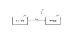
- a television receiver includes the liquid crystal display device and a tuner unit that receives a television broadcast.
- the active matrix substrate manufacturing method includes a data signal line extending in a column direction, a transistor connected to the scan signal line and the data signal line, and a storage capacitor line when the extending direction of the scanning signal line is a row direction.
- the first and second pixel electrodes and the first and second capacitor electrodes are formed as follows, that is, the first and second pixel electrodes are formed in one pixel region. Two pixel electrodes and first and second capacitor electrodes formed in the same layer as the data signal line are provided, and the first and second capacitor electrodes overlap with the storage capacitor line through the first insulating film.
- the wiring and the second connection wiring connected to the second capacitor electrode are electrically connected so that at least a part of the first connection wiring and at least a part of the second connection wiring do not overlap the storage capacitor wiring. If the first capacitor electrode and the data signal line are short-circuited, the first connection wiring is disconnected, and if the second capacitor electrode and the data signal line are short-circuited, the second connection wiring is formed. And a second step of cutting.
- the third capacitor electrode is connected to the second pixel electrode through a contact hole and overlaps with the storage capacitor wiring, and the first to third capacitor electrodes are connected to each other. If the third capacitor electrode and the data signal line are short-circuited in this order, the portion in the contact hole of the second pixel electrode may be removed.
- a transistor connected to the scanning signal line of the present invention and a storage capacitor line are provided, and one pixel region includes first and second pixel electrodes, first and second capacitor electrodes, and first and second capacitors.
- the first and second capacitor electrodes overlap with the storage capacitor line via the first insulating film, and each of the first and second capacitor electrodes overlaps the storage capacitor line via the second insulating film.
- one of the conductive electrodes of the transistor and the connection wiring are electrically connected, and one or the other conductive electrode of the transistor and the first pixel electrode are electrically connected, and at least one of the connection wirings A part thereof does not overlap with the storage capacitor wiring.
- the production yield of the active matrix substrate can be increased.
- FIG. 2 is a cross-sectional view of the liquid crystal panel of FIG. 1 taken along arrows XY and XZ.
- FIG. 2 is an equivalent circuit diagram of the liquid crystal panel of FIG. 1.
- 3 is a timing chart illustrating a driving method of a liquid crystal display device including the liquid crystal panel of FIG. 1.
- FIG. 5 is a schematic diagram showing a display state for each frame when the driving method of FIG. 4 is used. It is a top view which shows the correction method of the liquid crystal panel of FIG. It is a top view which shows the example of a defect generation
- FIG. 10 is a cross-sectional view of the liquid crystal panel of FIG.
- FIG. 10 is a plan view illustrating still another specific example of the liquid crystal panel illustrated in FIG. 1.
- FIG. 12 is a cross-sectional view of the liquid crystal panel of FIG.
- FIG. 10 is a plan view illustrating still another specific example of the liquid crystal panel illustrated in FIG. 1.
- FIG. 10 is a plan view illustrating still another specific example of the liquid crystal panel illustrated in FIG. 1.
- FIG. 15 is a plan view illustrating another specific example of the liquid crystal panel illustrated in FIG. 14.
- FIG. 10 is a plan view illustrating still another specific example of the liquid crystal panel illustrated in FIG. 1.
- FIG. 10 is a plan view illustrating still another specific example of the liquid crystal panel illustrated in FIG. 1.
- FIG. 17 is a plan view illustrating another specific example of the liquid crystal panel illustrated in FIG. 16.
- FIG. 10 is a plan view illustrating still another specific example of the liquid crystal panel illustrated in FIG. 1.
- FIG. 19 is a plan view illustrating another specific example of the liquid crystal panel illustrated in FIG. 18. It is a top view which shows the other structure of this liquid crystal panel.
- FIG. 10 is a plan view illustrating another specific example of the liquid crystal panel illustrated in FIG. 9.
- FIG. 22 is a cross-sectional view of the liquid crystal panel of FIG.
- FIG. 12 is a plan view illustrating another specific example of the liquid crystal panel illustrated in FIG. 11.
- FIG. 24 is a cross-sectional view of the liquid crystal panel of FIG. It is a top view which shows the modification of the liquid crystal panel shown in FIG.
- FIG. 27 is a plan view showing a modification of the liquid crystal panel shown in FIG. 26.
- FIG. 27 is a plan view showing a modification of the liquid crystal panel shown in FIG. 26.
- FIG. 27 is a plan view showing a modification of the liquid crystal panel shown in FIG. 26.
- FIG. 30 is a plan view showing a modification of the liquid crystal panel shown in FIG. 29.
- FIG. 31 is a plan view showing a modification of the liquid crystal panel shown in FIG. 30.
- (A) is a schematic diagram which shows the structure of this liquid crystal display unit
- (b) is a schematic diagram which shows the structure of this liquid crystal display device. It is a block diagram explaining the whole structure of this liquid crystal display device.
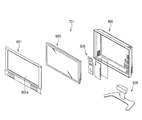
- FIG. 26 is a block diagram illustrating functions of the present television receiver. It is a disassembled perspective view which shows the structure of this television receiver. It is a top view which shows other structure of this liquid crystal panel. It is a top view which shows the structure of the conventional liquid crystal panel.
- the extending direction of the scanning signal lines is hereinafter referred to as the row direction.
- the scanning signal line may extend in the horizontal direction or in the vertical direction. Needless to say, it is good.
- the alignment regulating structure is omitted as appropriate.
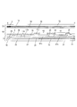
- FIG. 3 is an equivalent circuit diagram showing a part of the liquid crystal panel according to the present embodiment.
- the present liquid crystal panel is arranged in the column direction (up and down direction in the drawing), the data signal line 15 extending in the row direction (scanning signal line 16 extending in the left and right direction in the drawing), and the row and column direction.
- the pixels (101 to 104) Provided with the pixels (101 to 104), the storage capacitor wiring 18, and the common electrode (counter electrode) com, the structure of each pixel is the same. Note that the pixel column including the pixels 101 and 102 and the pixel column including the pixels 103 and 104 are adjacent to each other, and the pixel row including the pixels 101 and 103 and the pixel row including the pixels 102 and 104 are adjacent to each other. is doing.
- one data signal line 15, one scanning signal line 16, and one storage capacitor line 18 are provided corresponding to one pixel, and three pixel electrodes (17a) are provided for one pixel. 17c), and these three pixel electrodes are arranged in the column direction.
- the pixel electrode 17a is connected to the data signal line 15 via the transistor 12 connected to the scanning signal line 16, the pixel electrodes 17a and 17c are electrically connected, and the pixel electrodes 17a and 17c and the pixel are connected.
- the electrode 17b is connected via the coupling capacitor Cc, the storage capacitor Ch1 is formed between the pixel electrodes 17a and 17c and the storage capacitor line 18, and the storage capacitor Ch2 is formed between the pixel electrode 17b and the storage capacitor line 18.
- the liquid crystal capacitor Cl1 is formed between the pixel electrodes 17a and 17c and the common electrode com, and the liquid crystal capacitor Cl2 is formed between the pixel electrode 17b and the common electrode com.
- the pixel electrode 17a is connected to the data signal line 15 (via the transistor 12).
- the pixel electrodes 17a and 17c and the pixel electrode 17b are coupled via the coupling capacitor Cc, the potential of the pixel electrode 17a and the pixel electrode 17c after the transistor 12 is turned off is Vac, and the transistor 12 is turned off.
- the potential of the subsequent pixel electrode 17b is Vb,
- means a potential difference between Vb and com potential Vcom).
- the sub-pixel including the pixel electrode 17a is a bright sub-pixel
- the sub-pixel including the pixel electrode 17b is a dark sub-pixel
- the sub-pixel including the pixel electrode 17c is a bright sub-pixel.
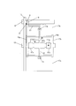
- FIG. 1 shows a specific example of the pixel 101 in FIG.
- a transistor 12 is arranged in the vicinity of the intersection of the data signal line 15 and the scanning signal line 16, and three pixel electrodes (first and second) are formed in a pixel region defined by both signal lines (15, 16).
- the first to third pixel electrodes 17a to 17c each have a rectangular shape, and are arranged in this order in the column direction.
- the storage capacitor line 18 extends in the row direction so as to cross the center of the pixel (so as to overlap the second pixel electrode 17b).
- the first to third capacitor electrodes 67x to 67z are arranged in the row direction in this order so as to overlap the storage capacitor line 18 through a gate insulating film (not shown).
- Each of 67x to 67z overlaps the second pixel electrode 17b via an interlayer insulating film (not shown). That is, the second capacitor electrode 67y is disposed below the center of the second pixel electrode 17b, and the first capacitor electrode is disposed between one of the two adjacent data signal lines (data signal line 15) and the second capacitor electrode 67y.
- 67x is arranged, and the first capacitance electrode 67z is arranged between the other and the second capacitance electrode 67y.
- the source electrode 8 of the transistor 12 is connected to the data signal line
- the drain electrode 9 is connected to the second capacitor electrode 67y via the drain lead line 27
- the drain lead line 27 is connected to the pixel electrode 17a via the contact hole 11a. It is connected to the.
- the drain lead-out wiring 27 is connected to the first connection wiring 38 in the same layer, and is connected to the second connection wiring 39 in the same layer.
- the first connection wiring 38 is connected to the first capacitor electrode 67x
- the second The connection wiring 39 is connected to the first capacitor electrode 67y.
- the first and second connection wirings 38 and 39 are both provided so as not to overlap the storage capacitor wiring 18.
- the second capacitor electrode 67y is connected to the relay wiring 47, and the relay wiring 47 is connected to the pixel electrode 17c through the contact hole 11c.
- the drain electrode 9 of the transistor 12, the first pixel electrode 17a, the first connection wiring 38, and the second connection wiring 39 are electrically connected, and the overlapping portion of the first capacitance electrode 67x and the second pixel electrode 17b is connected.
- a coupling capacitor Cc (see FIG. 3) is formed at the overlapping portion of the second capacitor electrode 67y and the second pixel electrode 17b.
- a storage capacitor Ch1 is formed at the overlapping portion between the first and second capacitor electrodes 67x and 67y and the storage capacitor wiring 18.
- the third capacitor electrode 67z and the second pixel electrode 17b are connected via the contact hole 11bz, and as a result, most of the storage capacitor Ch2 is added to the overlapping portion of the third capacitor electrode 67z and the storage capacitor wiring 18. It is formed.
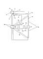
- the present liquid crystal panel includes an active matrix substrate 3, a color filter substrate 30 facing the active matrix substrate 3, and a liquid crystal layer 40 disposed between the substrates (3, 30).
- the scanning signal lines 16 and the storage capacitor lines 18 are formed on the glass substrate 31, and an inorganic gate insulating film 22 (for example, SiNx) is formed so as to cover them.
- the upper layer of the inorganic gate insulating film 22 includes a semiconductor layer (i layer and n + layer), a source electrode and a drain electrode in contact with the n + layer, a relay wiring 47, and a first connection.
- a wiring 38 is formed.
- an inorganic interlayer insulating film 25 (for example, SiNx) is formed so as to cover the metal layer.
- First and second pixel electrodes 17a and 17b are formed on the inorganic interlayer insulating film 25, and an alignment film 9 is formed so as to cover these pixel electrodes.
- the inorganic interlayer insulating film 25 is penetrated, and thereby the first pixel electrode 17a and the drain lead wiring 27 are connected.
- the inorganic interlayer insulating film 25 is penetrated, whereby the second pixel electrode 17b and the third capacitor electrode 67z are connected.
- each of the first capacitor electrode 67x and the second capacitor electrode 67y overlaps the second pixel electrode 17b through the inorganic interlayer insulating film 25, and a coupling capacitor Cc (see FIG. 3) is formed here. Further, each of the first capacitor electrode 67x and the second capacitor electrode 67y overlaps the storage capacitor wiring 18 through the inorganic gate insulating film 22, and the storage capacitor Ch1 (see FIG. 3) is formed here. Further, the third capacitor electrode 67z overlaps the storage capacitor wiring 18 through the inorganic gate insulating film 22, and most of the storage capacitor Ch2 (see FIG. 3) is formed here.
- a colored layer (color filter layer) 14 is formed on a glass substrate 32, a common electrode (com) 28 is formed thereon, and an alignment film 19 is formed so as to cover this. ing.
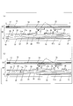
- FIG. 4 is a timing chart showing a driving method of the present liquid crystal display device (normally black mode liquid crystal display device) provided with the liquid crystal panel shown in FIGS.
- Sv and SV represent signal potentials supplied to two adjacent data signal lines
- Gp represents a gate-on pulse signal supplied to the scanning signal line 16
- Va to Vc represent pixel electrodes 17a to 17c, respectively. The potential of 17c is shown.
- the scanning signal lines are sequentially selected, the polarity of the signal potential supplied to the data signal lines is inverted every horizontal scanning period (1H), and the same number in each frame.
- the polarity of the signal potential supplied in the horizontal scanning period is inverted in units of one frame, and in the same horizontal scanning period, a signal potential having a reverse polarity is supplied to two adjacent data signal lines.
- scanning signal lines are sequentially selected, and one of two adjacent data signal lines has an nth horizontal scanning period (for example, the pixel electrode 17a).
- a positive polarity signal potential is supplied during the (n + 1) th horizontal scanning period, and a negative polarity signal potential is supplied during the (n + 1) th horizontal scanning period.
- the other of the two data signal lines is connected to the nth horizontal scanning period. Is supplied with a negative signal potential, and a positive signal potential is supplied during the (n + 1) th horizontal scanning period.
- the subpixel including the pixel electrode 17a (positive polarity) is a bright subpixel (hereinafter, “bright”), and the pixel electrode 17b.
- the sub-pixel including (plus polarity) is a dark sub-pixel (hereinafter “dark”), and the sub-pixel including the pixel electrode 17c (plus polarity) is “bright”, as a whole, as shown in FIG. .
- scanning signal lines are sequentially selected, and a negative signal potential is applied to one of the two adjacent data signal lines in the nth horizontal scanning period (for example, including the writing period of the pixel electrode 17a).
- a positive polarity signal potential is supplied during the (n + 1) th horizontal scanning period, and a positive polarity signal potential is supplied during the nth horizontal scanning period to the other of the two data signal lines.
- a negative polarity signal potential is supplied in the (n + 1) th horizontal scanning period.
- the subpixel including the pixel electrode 17a (negative polarity) is a bright subpixel (hereinafter, “bright”), and the pixel electrode 17b.
- the sub-pixel including (minus polarity) is a dark sub-pixel (hereinafter “dark”), and the sub-pixel including the pixel electrode 17c (minus polarity) is “bright”, as a whole, as shown in FIG. .
- each pixel electrode is provided with a slit for regulating the alignment
- the color filter The substrate is provided with orientation regulating ribs.
- an alignment regulating slit may be provided in the common electrode of the color filter substrate.
- the drain electrode 9 of the transistor, the first pixel electrode 17a, the first connection wiring 38 connected to the first capacitance electrode 67x, and the second connection wiring 39 connected to the second capacitance electrode 67y Are electrically connected, so that even if the first capacitance electrode 67x adjacent to the data signal line is short-circuited to the data signal line, the values of the coupling capacitor and the holding capacitor are not greatly reduced. It has a configuration that can. That is, when the data signal line 15 and the first capacitor electrode 67x are short-circuited, the first connection wiring 38 may be cut as shown in FIG. In this case, it is possible to normally control the potential of the first to third pixel electrodes 17a to 17c (normally drive the three subpixels) by the second capacitor electrode 67y.
- the pixel electrode in the contact hole 11bz is trimmed away as shown in FIGS. 8 (a) and 8 (b). Can fix this. In this case, it is possible to normally control the potential of the first to third pixel electrodes 17a to 17c (normally drive the three subpixels). Further, even if the second capacitor electrode 67y and the third capacitor electrode 67z are short-circuited, the potential supplied to the first and third pixel electrodes 17a and 17c is only supplied to the second pixel electrode 17b. And the potential control of the third pixel electrodes 17a and 17c is not disabled.
- the method for manufacturing a liquid crystal panel includes an active matrix substrate manufacturing process, a color filter substrate manufacturing process, and an assembly process in which both substrates are bonded to each other and filled with liquid crystal.
- a metal film such as titanium, chromium, aluminum, molybdenum, tantalum, tungsten, or copper, an alloy film thereof, or a laminated film thereof (thickness: 1000 mm to 3000 mm) is sputtered onto a substrate such as glass or plastic. Then, patterning is performed by photolithography technology (Photo Engraving Process, hereinafter referred to as “PEP technology”), and scanning signal lines and gate electrodes of transistors (scanning signal lines may also serve as gate electrodes) ) And a storage capacitor wiring.
- PEP technology Photo Engraving Process
- an inorganic insulating film such as silicon nitride or silicon oxide is formed by CVD (Chemical Vapor Deposition) method on the entire substrate on which the scanning signal lines are formed, thereby forming a gate insulating film To do.
- an intrinsic amorphous silicon film (thickness 1000 to 3000 mm) and an n + amorphous silicon film (thickness 400 to 700 mm) doped with phosphorus are continuously formed on the gate insulating film (whole substrate) by CVD.
- patterning is performed by the PEP technique, and a silicon laminated body including an intrinsic amorphous silicon layer and an n + amorphous silicon layer is formed in an island shape on the gate electrode.
- a metal film such as titanium, chromium, aluminum, molybdenum, tantalum, tungsten, or copper, an alloy film thereof, or a stacked film thereof (thickness 1000 to 3000 mm) is formed on the entire substrate on which the silicon laminate is formed. Then, patterning is performed by the PEP technique, and data signal lines, transistor source / drain electrodes, drain lead-out wiring, capacitor electrodes, relay wiring, and connection wiring (metal layer) are formed. Form.
- the n + amorphous silicon layer constituting the silicon stacked body is removed by etching to form a transistor channel.
- the semiconductor layer may be formed of an amorphous silicon film as described above.
- a polysilicon film may be formed, or a laser annealing treatment is performed on the amorphous silicon film and the polysilicon film to form a crystal. May be improved. Thereby, the moving speed of the electrons in the semiconductor layer is increased, and the characteristics of the transistor (TFT) can be improved.
- an inorganic insulating film such as silicon nitride or silicon oxide is formed by CVD on the entire substrate on which the data signal lines and the like are formed to form an inorganic interlayer insulating film.
- the interlayer insulating film is etched away by PEP technology to form a contact hole.
- a transparent conductive film (thickness 1000 to 2000 mm) made of ITO (Indium / Tin / Oxide), IZO (Indium / Zinc / Oxide), zinc oxide, tin oxide or the like is formed on the entire substrate on the interlayer insulating film in which the contact holes are formed. Is formed by sputtering, and then patterned by PEP technology to form each pixel electrode.
- polyimide resin is printed on the entire substrate on the pixel electrode with a thickness of 500 to 1000 mm, and then fired and rubbed in one direction with a rotating cloth to form an alignment film.
- the active matrix substrate is manufactured as described above.
- the color filter substrate manufacturing process will be described below.
- a chromium thin film or a resin containing a black pigment is formed on a glass or plastic substrate (entire substrate), and then patterned by PEP technology to form a black matrix.
- red, green and blue color filter layers are formed in a pattern in the gap of the black matrix by using a pigment dispersion method or the like.
- a transparent conductive film made of ITO, IZO, zinc oxide, tin oxide or the like is formed on the entire substrate on the color filter layer to form a common electrode (com).
- polyimide resin is printed on the entire substrate on the common electrode with a thickness of 500 to 1000 mm, and then fired and rubbed in one direction with a rotating cloth to form an alignment film.
- a color filter substrate can be manufactured as described above.
- a seal material made of a thermosetting epoxy resin or the like is applied to one of the active matrix substrate and the color filter substrate by screen printing in a frame-like pattern lacking the liquid crystal inlet portion, and the liquid crystal layer is applied to the other substrate.
- a spherical spacer having a diameter corresponding to the thickness and made of plastic or silica is dispersed.
- the active matrix substrate and the color filter substrate are bonded together, and the sealing material is cured.
- the liquid crystal panel is manufactured.
- an inspection process is performed during or after at least one of the active matrix substrate manufacturing process and the assembly process, and when a defect such as a short circuit is detected in the inspection process, a correction process for correcting the defect is added.
- a correction process for cutting the first connection wiring 38 by laser is performed.
- a fourth harmonic wavelength 266 nm
- YAG Yttrium Aluminum Garnet
- This correction process can be performed either during the production of the active matrix substrate (after the metal layer formation stage) and after completion, or after completion of the liquid crystal panel.
- a correction process can be performed at the metal layer formation stage or the transistor channel formation stage. is there.
- the short circuit portion may be removed by a laser or the like.
- the second pixel electrode 17b when it is found that the data signal line 15 and the third capacitor electrode 67z are short-circuited in the inspection process after the pixel electrode is formed (for example, when the active matrix substrate is completed) (see FIG. 7), the second pixel electrode 17b.
- a correction step of trimming and removing the portion in the contact hole 11bz with a laser or the like may be performed (see FIGS. 8A and 8B). If it is found by inspection after completion of the liquid crystal panel that the data signal line 15 and the third capacitor electrode 67z are short-circuited, it is difficult to perform a correction process for trimming and removing the pixel electrode. This is because the YAG laser is absorbed by the color filter (CF) substrate.
- CF color filter
- the YAG laser is not absorbed by the color filter substrate, so even after the liquid crystal panel is completed, for example, the third harmonic or the fourth harmonic of the YAG laser is used. It is possible to perform (a correction process for trimming and removing the pixel electrode).
- a thicker organic interlayer insulating film 26 (for example, acrylic resin) is provided on the inorganic interlayer insulating film 25 of FIG. 2, and an interlayer insulating film (channel protective film) is formed as shown in FIG. A two-layer (25/26) structure may also be used.
- an interlayer insulating film channel protective film
- effects such as reduction of various parasitic capacitances, prevention of short-circuiting between wirings, and reduction of pixel electrode tearing due to planarization can be obtained.
- the organic interlayer insulating film 26 penetrates the portion K1 overlapping the first capacitor electrode 67x and the portion K2 overlapping the second capacitor electrode 67y. .
- the above-described effect can be obtained while sufficiently securing the capacitance value of the coupling capacitance (Cc in FIG. 3).
- the aperture ratio can be increased by overlapping the scanning signal line 16 and the first pixel electrode 17a as shown in FIGS.
- the inorganic interlayer insulation film 25, the organic interlayer insulation film 26, and the contact hole 11a of FIG. 10 can be formed as follows, for example. That is, after forming the transistors and data signal lines, an inorganic interlayer insulating film 25 made of SiNx having a thickness of about 3000 mm so as to cover the entire surface of the substrate using a mixed gas of SiH 4 gas, NH 3 gas, and N 2 gas. (Passivation film) is formed by CVD. Thereafter, an organic interlayer insulating film 26 made of a positive photosensitive acrylic resin having a thickness of about 3 ⁇ m is formed by spin coating or die coating.
- photolithography is performed to form a penetrating portion of the organic interlayer insulating film 26 and various contact patterns. Further, using the patterned organic interlayer insulating film 26 as a mask, CF 4 gas and O 2 gas The inorganic interlayer insulating film 25 is dry-etched using a mixed gas. Specifically, for example, the penetration portion of the organic interlayer insulating film is half-exposed in the photolithography process so that the organic interlayer insulating film remains thin when development is completed, while the contact hole portion is By performing full exposure in the photolithography process, an organic interlayer insulating film is not left when development is completed.
- the organic interlayer insulating film 26 may be, for example, an insulating film made of an SOG (spin-on glass) material, and the organic interlayer insulating film 26 may be an acrylic resin, an epoxy resin, a polyimide resin, a polyurethane resin, or a novolac resin. , And at least one of siloxane resins may be included.
- an organic gate insulating film 21 thicker than this is provided under the inorganic gate insulating film 22 in FIG. 2, and the gate insulating film has a two-layer (21.22) structure as shown in FIG. You can also. In this way, effects such as reduction of various parasitic capacitances, prevention of short-circuiting of wirings, and reduction of disconnection rate of data signal lines, drain lead-out wirings, and the like due to planarization can be obtained. In this case, as shown in FIGS. 11 and 12, it is more preferable that the organic gate insulating film 21 penetrates the portion F overlapping with the first to third capacitor electrodes 67x to 67z.
- the above-described effect can be obtained while sufficiently securing the capacitance value of the storage capacitors (Ch1 and Ch2 in FIG. 3).
- the aperture ratio can be increased by overlapping the scanning signal line 16 and the first pixel electrode 17a as shown in FIGS. .
- the first connection wiring 38 is arranged so that a part thereof overlaps the gap between the first pixel electrode 17a and the second pixel electrode 17b. By doing so, the cutting process of the first connection wiring 38 is facilitated, and light leakage between the pixel electrodes can be reduced.
- FIG. 1 can be modified as shown in FIG.
- a storage capacitor wiring extending portion 18 p extending along the data signal line 15 in a plan view from the storage capacitor wiring 18 and a data signal adjacent to the data signal line 15 in a plan view.
- the storage capacitor wiring extending portion 18q extending along the line extends, and the storage capacitor wiring extending portion 18p overlaps one of the two edges along the data signal line of the second pixel electrode 17b (the edge on the data signal line 15 side).
- the storage capacitor wiring extension 18q overlaps the other of the two edges.
- the storage capacitor wiring extending portions 18p and 18q function as shield electrodes of the pixel electrode 17b (floating pixel electrode), and therefore, it is possible to more effectively suppress charge jumping into the pixel electrode 17b. Thereby, the burn-in of the sub-pixel (dark sub-pixel) including the pixel electrode 17b can be suppressed.
- the interlayer insulating film may have a two-layer structure of an inorganic interlayer insulating film and an organic interlayer insulating film.
- effects such as reduction of various parasitic capacitances, prevention of short-circuiting between wirings, and reduction of pixel electrode tearing due to planarization can be obtained.
- the above-described effects can be obtained while ensuring a sufficient capacitance value of the coupling capacitance (Cc in FIG. 3) and ensuring the shielding effect by the storage capacitor wiring extending portions 18p and 18q.
- the aperture ratio can be increased by overlapping the scanning signal line 16 and the first pixel electrode 17a as shown in FIG.
- the storage capacitor is formed at the overlapping portion of the storage capacitor wiring 18 and the second pixel electrode 17b, it is suitable when the interlayer insulating film covering the TFT channel is relatively thin.
- the first capacitor electrode 67x is short-circuited with the data signal line, it is possible to maintain the capacitive coupling of the first and second pixel electrodes 17a and 17b by cutting the first connection wiring 38. Become.
- the capacitive coupling between the first and second pixel electrodes 17a and 17b can be maintained by cutting the second connection wiring 39. .
- FIG. 16 can be modified as shown in FIG. In the liquid crystal panel shown in FIG. 17, a part of the first connection wiring 38 connected to the first capacitance electrode 67x adjacent to the data signal line overlaps the gap between the first pixel electrode 17a and the second pixel electrode 17b. By doing so, the cutting process of the first connection wiring 38 is facilitated, and light leakage between the pixel electrodes can be reduced.
- a subpixel including the pixel electrode 17 a is a bright subpixel
- a subpixel including the pixel electrode 17 b is a dark subpixel. Display can be performed by area gradation of one dark sub-pixel.
- the liquid crystal panel 18 can be modified as shown in FIG.
- a part of the first connection wiring 38 connected to the first capacitance electrode 67x adjacent to the data signal line overlaps the gap between the first pixel electrode 17a and the second pixel electrode 17b.
- the cutting process of the first connection wiring 38 is facilitated, and light leakage between the pixel electrodes can be reduced.
- the liquid crystal panel of FIG. 19 can be configured as shown in FIG. 25 except for the third capacitor electrode 67z and the contact hole 11bz. In this configuration, since the storage capacitor is formed at the overlapping portion of the storage capacitor wiring 18 and the second pixel electrode 17b, it is suitable when the interlayer insulating film covering the TFT channel is relatively thin.
- FIG. 20 is a plan view showing another configuration of the present liquid crystal panel.
- the first pixel in the pixel region defined by the data signal line 15 and the scanning signal line 16, the first pixel having a shape that fits with the trapezoidal second pixel electrode 17b when viewed in the row direction.
- the electrodes 17a are arranged in the row direction, and the storage capacitor wiring 18 extends in the row direction so as to cross the center of the pixel (so as to overlap the second pixel electrode 17b).
- the outer periphery of the second pixel electrode 17b intersects the storage capacitor line 18, forms a first side that forms approximately 90 ° with respect to the row direction, and forms approximately 45 ° with respect to the row direction from one end of the first side.
- a second side extending from the other end of the first side, a third side extending at about 315 ° with respect to the row direction, and a fourth side parallel to the first side and intersecting the storage capacitor wiring 18
- the first side is the upper base of the trapezoid
- the fourth side is the lower base of the trapezoid
- the line connecting the midpoints of the first and fourth sides passes over the storage capacitor wiring 18.
- the outer periphery of the first pixel electrode 17 a includes Three sides opposite to the third side are included, and the gap between the first side of the second pixel electrode 17b and one side of the outer periphery of the first pixel electrode 17a opposite to the first side is the first gap S1 and the second pixel.
- the gap between the second side of the electrode 17b and one side of the outer periphery of the first pixel electrode 17a opposite to the second side is the second gap S2, and the outer side of the third side of the second pixel electrode 17b and the first pixel electrode 17a opposite to the third side.
- a gap with one side is a third gap S3.
- the first to third capacitor electrodes 67x to 67z are arranged in the row direction in this order so as to overlap the storage capacitor line 18 through a gate insulating film (not shown).
- Each of 67x to 67z overlaps the second pixel electrode 17b via an interlayer insulating film (not shown). That is, the second capacitor electrode 67y is disposed below the center of the second pixel electrode 17b, and the first capacitor electrode is disposed between one of the two adjacent data signal lines (data signal line 15) and the second capacitor electrode 67y.
- 67x is arranged, and the first capacitance electrode 67z is arranged between the other and the second capacitance electrode 67y.
- the source electrode 8 of the transistor 12 is connected to the data signal line
- the drain electrode 9 is connected to the second capacitor electrode 67y via the drain lead line 27
- the drain lead line 27 is connected to the pixel electrode 17a via the contact hole 11a. It is connected to the.
- the drain lead-out wiring 27 is connected to the first connection wiring 38 in the same layer, and is connected to the second connection wiring 39 in the same layer.
- the first connection wiring 38 is connected to the first capacitor electrode 67x
- the second The connection wiring 39 is connected to the first capacitor electrode 67y.
- the first and second connection wirings 38 and 39 are both provided so as not to overlap the storage capacitor wiring 18.
- the drain electrode 9 of the transistor 12, the first pixel electrode 17a, the first connection wiring 38, and the second connection wiring 39 are electrically connected, and the overlapping portion of the first capacitance electrode 67x and the second pixel electrode 17b is connected.
- a coupling capacitor is formed at the overlapping portion of the second capacitor electrode 67y and the second pixel electrode 17b.
- a storage capacitor is formed in an overlapping portion between the first and second capacitor electrodes 67x and 67y and the storage capacitor wiring 18.
- the third capacitor electrode 67z and the second pixel electrode 17b are connected via the contact hole 11bz, whereby a storage capacitor is formed at the overlapping portion of the third capacitor electrode 67z and the storage capacitor wiring 18. .
- a storage capacitor wiring extending portion 18p extending along the data signal line 15 in plan view from the storage capacitor wiring 18, and a storage capacitor extending along the data signal line adjacent to the data signal line 15 in plan view.
- the wiring extending portion 18q extends, the storage capacitor wiring extending portion 18p overlaps with the first side on the outer periphery of the second pixel electrode 17b, and the storage capacitor wiring extending portion 18q extends on the fourth side on the outer periphery of the second pixel electrode 17b. overlapping.
- the drain electrode 9 of the transistor, the first pixel electrode 17a, the first connection wiring 38 connected to the first capacitance electrode 67x, and the second connection wiring 39 connected to the second capacitance electrode 67y Are electrically connected, so that even if the capacitance electrode (first capacitance electrode 67x) closer to the data signal line is short-circuited to the data signal line while maintaining the values of the coupling capacitance and the holding capacitance, It is the composition which can be corrected. That is, when the data signal line 15 and the first capacitor electrode 67x are short-circuited, the first connection wiring 38 may be cut. In this case, the potential of the first and second pixel electrodes 17a and 17b can be normally controlled (the two subpixels are normally driven) by the second capacitor electrode 67y.
- the data signal line 15 and the third capacitor electrode 67z are short-circuited, this can be corrected by removing the pixel electrode in the contact hole 11bz. In this case, it is possible to normally control the potential of the first and second pixel electrodes 17a and 17b (normally drive the two subpixels). Further, even if the second capacitor electrode 67y and the third capacitor electrode 67z are short-circuited, the potential supplied to the first pixel electrode 17a is only supplied to the second pixel electrode 17b, and the first and second pixel electrodes. The potential control of 17a and 17b is not disabled.
- the second gap S2 or the third gap S3 can function as an alignment regulating structure. Furthermore, since the storage capacitor line extending portions 18p and 18q function as a shield electrode of the second pixel electrode 17b (floating pixel electrode), it is possible to more effectively suppress the jumping of charges into the second pixel electrode 17b. it can. Thereby, the burn-in of the sub-pixel (dark sub-pixel) including the second pixel electrode 17b can be suppressed.
- the interlayer insulating film may have a two-layer structure of an inorganic interlayer insulating film and an organic interlayer insulating film.
- the organic interlayer insulating film penetrates through a portion overlapping the first capacitor electrode 67x, a portion overlapping the second capacitor electrode 67y, and a portion overlapping the storage capacitor wiring extending portions 18p and 18q. . In this way, the above-described effect can be obtained while ensuring a sufficient capacitance value of the coupling capacitance and ensuring the shielding effect by the storage capacitor wiring extending portions 18p and 18q.
- the liquid crystal panel shown in FIGS. 9 and 10 can be configured as shown in FIGS.
- portions D1 and D2 corresponding to the penetration portions K1 and K2 of the organic interlayer insulating film 26 of the active matrix substrate 3 are raised.
- the depression of the surface of the active matrix substrate due to the punched-out portions K1 and K2 can be compensated, and the thickness of the liquid crystal layer under the raised portions D1 and D2 can be made the same as the surroundings. Thereby, the thickness of the liquid crystal layer can be made uniform, and the amount of liquid crystal used can be reduced.
- a protruding member i is provided on the counter electrode 28, thereby forming the raised portions D1 and D2 on the surface of the color filter substrate. Therefore, even if the conductive foreign material falls into the depression on the surface of the active matrix substrate due to the punched-out portion K, a short circuit between the second pixel electrode 17b and the counter electrode 28 can be prevented.
- the protruding member i can be formed in the same process (same material) as the orientation regulating rib (for example, phenol novolac resin). In FIG.
- a protruding member j is provided on the colored layer 14 (below the counter electrode 28), thereby forming the raised portions D1 and D2 on the surface of the color filter substrate.
- the protruding member j may be a colored layer having a different color from the colored layer 14, and the raised portions D1 and D2 may be formed by superimposing these colored layers (for example, an R colored layer and a G colored layer). In this case, there is an advantage that the protruding member does not need to be formed separately (made of another material).
- the distance between the second pixel electrode 17b and the counter electrode 28 under the raised portions D1 and D2 can be shortened as compared with the configuration in which the raised portions D1 and D2 are not formed.
- the liquid crystal capacity can be increased.
- the holding capacitor wiring It is desirable to have a configuration that fits between two edges along 18 row directions.
- the liquid crystal panel shown in FIGS. 11 and 12 can be configured as shown in FIGS.
- a portion D corresponding to the penetration portion F of the organic gate insulating film 21 of the active matrix substrate 3 is raised.
- the depression of the surface of the active matrix substrate due to the punched-in portion F can be compensated, and the thickness of the liquid crystal layer under the raised portion D can be made the same as the surroundings. Thereby, the thickness of the liquid crystal layer can be made uniform, and the amount of liquid crystal used can be reduced.
- a protruding member i is provided on the counter electrode 28, thereby forming a raised portion D on the surface of the color filter substrate.
- the protruding member i can be formed in the same step as the alignment regulating rib.
- a protruding member j is provided on the colored layer 14 (under the counter electrode 28), thereby forming a raised portion D on the surface of the color filter substrate.
- the protruding member j may be a colored layer having a different color from the colored layer 14, and the raised portion D may be formed by superimposing these colored layers (for example, an R colored layer and a G colored layer).
- the protruding member does not need to be formed separately (made of another material).
- the distance between the second pixel electrode 17b and the counter electrode 28 under the raised portion D can be shortened as compared with the configuration in which the raised portion D is not formed, the liquid crystal capacitance is increased. can do.
- the row direction of the storage capacitor wiring 18 It is desirable to have a configuration that fits between two edges along the line.
- This liquid crystal panel can also be configured as shown in FIG. That is, the rectangular first to third pixel electrodes 17a to 17c are arranged in this order in the column direction, and the first capacitor electrode 67x, the third capacitor electrode 67z, and the second capacitor electrode 67y are gate insulating films (not shown). In this order, the first to third capacitor electrodes 67x to 67z are arranged in the row direction so as to overlap the storage capacitor wiring 18 via the interlayer insulating film (not shown). It overlaps with 17b. Further, the third capacitor electrode 67z is disposed below the center of the second pixel electrode 17b, and the first capacitor electrode is disposed between one of the two adjacent data signal lines (data signal line 15) and the third capacitor electrode 67z.
- the source electrode 8 of the transistor 12 is connected to the data signal line 15, the drain electrode 9 is connected to the drain lead wiring 27 in the same layer, and the drain lead wiring 27 is connected to the pixel electrode 17a through the contact hole 11a. ing.
- the first connection wiring 38 is L-shaped and includes a laterally extending portion 38 x extending in the same direction as the scanning signal line 16 and a longitudinally extending portion 38 y extending along the data signal line 15.
- the second connection wiring 39 is also L-shaped and includes a laterally extending portion 39 x extending in the same direction as the scanning signal line 16 and a longitudinally extending portion 39 y extending along the data signal line 215.
- one end (laterally extending portion 38x side) of the first connection wiring 38 is connected to the drain lead wiring 27, and the other end (vertical extending portion 38y side) is connected to the first capacitor electrode 67x.
- one end portion (laterally extending portion 39x side) of the second connecting wire 39 is connected to the drain lead wire 27, and the other end portion (vertically extending portion 39y side) is connected to the second capacitor electrode 67y. .
- the third connection wiring 58 is L-shaped and includes a longitudinally extending portion 58y along the data signal line 15 and a laterally extending portion 58x extending in the same direction as the scanning signal line 16.
- the fourth connection wiring 59 is also L-shaped, and includes a longitudinally extending portion 59 y along the data signal line 215 and a laterally extending portion 59 x extending in the same direction as the scanning signal line 16.
- one end portion (the longitudinally extending portion 58y side) of the third connecting wire 58 is connected to the first capacitor electrode 67x, and the other end portion (the laterally extending portion 58x side) is connected to the relay wire 147.
- one end portion (vertical extending portion 59 y side) of the fourth connection wiring 59 is connected to the second capacitor electrode 67 y, and the other end portion (lateral extending portion 59 x side) is connected to the relay wiring 147.
- the relay wiring 147 is connected to the third pixel electrode 17c through the contact hole 11c.
- laterally extending portion 38x of the first connecting wiring 38 and the laterally extending portion 39x of the second connecting wiring 39 are both disposed under the gap between the first pixel electrode 17a and the second pixel electrode 17b, and the storage capacitor wiring 18 and There is no overlap.
- the laterally extending portion 58x of the third connecting wiring 58 and the laterally extending portion 59x of the fourth connecting wiring 59 are both arranged under the gap between the second pixel electrode 17b and the third pixel electrode 17c, and the storage capacitor wiring 18 and There is no overlap.
- the drain electrode 9 of the transistor 12, the first pixel electrode 17a, the first connection wiring 38, and the second connection wiring 39 are electrically connected, and the overlapping portion of the first capacitance electrode 67x and the second pixel electrode 17b is connected.
- a coupling capacitor Cc (see FIG. 3) is formed at the overlapping portion of the second capacitor electrode 67y and the second pixel electrode 17b.
- a storage capacitor Ch1 (see FIG. 3) is formed at the overlapping portion between the first and second capacitor electrodes 67x and 67y and the storage capacitor wiring 18.
- the third capacitor electrode 67z and the second pixel electrode 17b are connected via the contact hole 11bz, and accordingly, the storage capacitor Ch2 (FIG. 3) is formed at the overlapping portion of the third capacitor electrode 67z and the storage capacitor wiring 18. Many of the references) are formed.
- the first connection wiring 38 and the third connection wiring 58 are respectively connected to the laser (for example, the third harmonic 355 nm of the YAG laser).
- the laser for example, the third harmonic 355 nm of the YAG laser.
- connection wirings 38, 39, 58, and 59
- four connection wirings 38, 39, 58, and 59
- the two laterally extending portions 38x and 39x disposed under the gap between the first pixel electrode 17a and the second pixel electrode 17b, and the gap between the second pixel electrode 17b and the third pixel electrode 17c,
- the two laterally extending portions 58x and 59x can be used as a light shielding member for suppressing light leakage.
- the coupling capacitance is formed in the portion where the four connection wirings (38, 39, 58, 59) and the pixel electrode 17b overlap, the first capacitance electrode 67x and the second capacitance are increased by the increase in the overlapping area.
- the electrode 67y can be made small, and the aperture ratio can be improved (or maintained).
- the pixel electrode 26 may be modified as shown in FIG. That is, the entire laterally extending portion 38x of the first connecting wiring 38, the laterally extending portion 39x of the second connecting wire 39, the laterally extending portion 58x of the third connecting wire 58, and the laterally extending portion 59x of the fourth connecting wire 59 are all formed.
- the pixel electrode is configured to be located under the gap between the pixel electrodes. By doing so, there is an advantage that there is less possibility that the connection wiring to be cut and the second pixel electrode 17b are short-circuited when each connection wiring is laser-cut.
- the longitudinally extending portion 38y of the first connecting wire 38 and the vertically extending portion 58y of the third connecting wire 58 are arranged so as to overlap the edge along the data signal line 15 of the second pixel electrode 17b, and the second connecting wire.
- the vertical extending portion 39y of 39 and the vertical extending portion 59y of the fourth connection wiring 59 are arranged so as to overlap with the edge along the data signal line 215 of the second pixel electrode 17b.
- the first connection wiring 38 is T-shaped, and includes a laterally extending portion 38 x extending in the same direction as the scanning signal line 16 and a longitudinally extending portion 38 y extending in the same direction as the data signal line 15.
- the second connection wiring 39 is also T-shaped and includes a laterally extending portion 39x extending in the same direction as the scanning signal line 16 and a longitudinally extending portion 39y extending in the same direction as the data signal line 215.
- the laterally extending portion 38x of the first connection wiring 38 is connected to the drain lead wiring 27, and the longitudinally extending portion 38y is connected to the first capacitor electrode 67x.
- the laterally extending portion 39x of the second connection wiring 39 is connected to the drain lead wiring 27, and the longitudinally extending portion 39y is connected to the second capacitor electrode 67y.
- the third connection wiring 58 includes only a laterally extending portion that overlaps the gap between the second pixel electrode 17b and the third pixel electrode 17c
- the fourth connection wiring 59 includes only a laterally extending portion that overlaps the gap.
- Each of the third and fourth connection wires 58 and 59 is connected to the relay wire 147.
- the relay wiring 147 is connected to the third pixel electrode 17c through the contact hole 11c.
- a transfer electrode 148 formed of the same material (same process) as each pixel electrode is arranged along the data signal line 15 in a plan view, and one end of the transfer electrode 148 and the first connection wiring 38 are connected to each other.
- the laterally extending portion 38x is connected by a contact hole, and the other end and the third connection wiring 58 are connected by a contact hole.
- a transfer electrode 149 formed of the same material (same process) as each pixel electrode is arranged along the data signal line 215 in plan view, and one end of the transfer electrode 149 and the second connection wiring 39
- the laterally extending portion 39x is connected by a contact hole, and the other end and the fourth connection wiring 59 are connected by a contact hole.
- the transfer electrode 248 along the data signal line 15 is connected in the same layer as the first pixel electrode 17a, and the other end is connected to the third pixel electrode 17c. Connect on the same layer.
- one end of the transfer electrode 249 along the data signal line 215 in a plan view is connected to the first pixel electrode 17a in the same layer, and the other end is connected to the third pixel electrode 17c in the same layer. In this way, the number of contact holes can be reduced as compared with the configuration of FIG.
- the inorganic interlayer insulating film may be formed as the channel protective film (insulating film between the data signal line and the pixel electrode), or the inorganic interlayer insulating film and the organic interlayer insulating film thicker than this may be formed.
- a film may be formed.
- the organic interlayer insulating film penetrate through the portion overlapping the first capacitor electrode 67x and the second pixel electrode 17b and the portion overlapping the second capacitor electrode 67y and the second pixel electrode 17b?
- FIG. 37 is a plan view showing another configuration of the present liquid crystal panel.
- the active matrix substrate of the liquid crystal panel of FIG. 37 includes transistors 112 and 212 connected to the scanning signal line 16 and a transistor 312 connected to the scanning signal line 116 that is the next stage of the scanning signal line 16.
- the pixel region includes pixel electrodes 17a and 17b, four capacitor electrodes 266x, 266y, 267x, and 267y, and a connection wiring 238 that connects the capacitor electrodes 267x and 267y.
- each of the capacitor electrodes 266x, 266y, 267x, and 267y overlaps the storage capacitor wiring 18 through the gate insulating film, and each of them is a channel protective film (inorganic interlayer insulating film or inorganic interlayer insulating film and organic interlayer insulating film).
- the drain electrode 308 of the transistor 312 and the capacitor electrode 267x are connected via the lead-out wiring 227, and the source electrode 309 of the transistor 312 and the pixel electrode 17a are contact holes.
- the connection wiring 238 is arranged so that at least a part thereof does not overlap the storage capacitor wiring 18.
- the common source electrode 128 of the transistors 112 and 212 is connected to the data signal line 15, the drain electrode 109 of the transistor 112 is connected to the capacitor electrode 266x via the lead wire 127p, and the capacitor electrode 266x is connected to the drain lead wire 127q and the contact.
- the capacitor electrode 266y is connected to the pixel electrode 17b through a contact hole, and is connected to the pixel electrode 17a through a hole. Note that the drain electrode 209 of the transistor 212 is connected to the pixel electrode 17b through a contact hole.
- a storage capacitor between the pixel electrode 17a and the storage capacitor wiring 18 is formed in an overlapping portion between the capacitor electrode 266x and the storage capacitor wiring 18, and a pixel electrode 17b and a storage capacitor are formed in the overlapping portion between the capacitor electrode 266y and the storage capacitor wiring 18.
- a storage capacitor between the capacitor wirings 18 is formed, and a coupling capacitor of the pixel electrode 17a and the pixel electrode 17b is formed in an overlapping portion between the capacitor electrodes 267x and 267y and the pixel electrode 17b.
- the same data signal potential is written to the pixel electrodes 17a and 17b when scanning the scanning signal line 16, but when scanning the scanning signal line 116 (next stage), the pixel electrodes 17a and 17b are scanned. 17b is connected via a capacitor. Thereby, a dark subpixel by the pixel electrode 17a and a bright subpixel by the pixel electrode 17b are formed. Even if the capacitor electrode 267y and the data signal line 115 are short-circuited, the coupling wiring 238 is cut at a portion that does not overlap the storage capacitor wiring 18, thereby maintaining the capacitive coupling between the pixel electrode 17a and the pixel electrode 17b. (A dark subpixel formed by the pixel electrode 17a and a bright subpixel formed by the pixel electrode 17b) can be formed.
- the present liquid crystal display unit and the liquid crystal display device are configured as follows. That is, the two polarizing plates A and B are attached to both surfaces of the liquid crystal panel so that the polarizing axis of the polarizing plate A and the polarizing axis of the polarizing plate B are orthogonal to each other. In addition, you may laminate
- drivers gate driver 202, source driver 201 are connected.
- ACF is temporarily pressure-bonded to the terminal portion of the liquid crystal panel.
- the TCP on which the driver is placed is punched out of the carrier tape, aligned with the panel terminal electrode, and heated and pressed.
- the circuit board 209 (PWB) for connecting the driver TCPs and the input terminal of the TCP are connected by ACF.
- the liquid crystal display unit 200 is completed.
- the display control circuit 209 is connected to each driver (201, 202) of the liquid crystal display unit via the circuit board 203, and integrated with the lighting device (backlight unit) 204.
- the liquid crystal display device 210 is obtained.
- FIG. 33 is a block diagram showing a configuration of the present liquid crystal display device.
- the liquid crystal display device includes a display unit (liquid crystal panel), a source driver (SD), a gate driver (GD), and a display control circuit.
- the source driver drives the data signal line
- the gate driver drives the scanning signal line
- the display control circuit controls the source driver and the gate driver.
- the display control circuit controls a display operation from a digital video signal Dv representing an image to be displayed, a horizontal synchronization signal HSY and a vertical synchronization signal VSY corresponding to the digital video signal Dv from an external signal source (for example, a tuner). For receiving the control signal Dc. Further, the display control circuit, based on the received signals Dv, HSY, VSY, and Dc, uses a data start pulse signal SSP and a data clock as signals for displaying an image represented by the digital video signal Dv on the display unit.
- Signal SCK digital image signal DA (signal corresponding to video signal Dv) representing an image to be displayed
- gate start pulse signal GSP gate start pulse signal GSP
- gate clock signal GCK gate driver output control signal (scanning signal output control signal) GOE is generated and these are output.
- the video signal Dv is output as a digital image signal DA from the display control circuit, and a pulse corresponding to each pixel of the image represented by the digital image signal DA.
- a data clock signal SCK is generated as a signal consisting of the above, a data start pulse signal SSP is generated as a signal that becomes high level (H level) for a predetermined period every horizontal scanning period based on the horizontal synchronization signal HSY, and the vertical synchronization signal VSY
- the gate start pulse signal GSP is generated as a signal that becomes H level only for a predetermined period every one frame period (one vertical scanning period), and the gate clock signal GCK is generated based on the horizontal synchronization signal HSY, and the horizontal synchronization signal HSY and
- a gate driver output control signal GOE is generated based on the control signal Dc.
- the digital image signal DA the polarity inversion signal POL for controlling the polarity of the signal potential (data signal potential)
- the data start pulse signal SSP the data start pulse signal SSP
- the data clock signal SCK the data clock signal SCK
- the gate start pulse signal GSP, the gate clock signal GCK, and the gate driver output control signal GOE are input to the gate driver.
- the source driver is based on the digital image signal DA, the data clock signal SCK, the data start pulse signal SSP, and the polarity inversion signal POL, and an analog potential (signal corresponding to the pixel value in each scanning signal line of the image represented by the digital image signal DA. Potential) is sequentially generated every horizontal scanning period, and these data signals are output to the data signal lines.
- the gate driver generates a gate-on pulse signal based on the gate start pulse signal GSP, the gate clock signal GCK, and the gate driver output control signal GOE, and outputs them to the scanning signal line, thereby selecting the scanning signal line. Drive.
- the data signal line and the scanning signal line of the display unit are driven by the source driver and the gate driver, so that the data is transmitted through the transistor (TFT) connected to the selected scanning signal line.
- TFT transistor
- a signal potential is written from the signal line to the pixel electrode.
- a voltage is applied to the liquid crystal layer of each subpixel, whereby the amount of light transmitted from the backlight is controlled, and an image indicated by the digital video signal Dv is displayed on each subpixel.
- FIG. 34 is a block diagram showing a configuration of a liquid crystal display device 800 for a television receiver.
- the liquid crystal display device 800 includes a liquid crystal display unit 84, a Y / C separation circuit 80, a video chroma circuit 81, an A / D converter 82, a liquid crystal controller 83, a backlight drive circuit 85, a backlight 86, A microcomputer 87 and a gradation circuit 89 are provided.
- the liquid crystal display unit 84 includes a liquid crystal panel and a source driver and a gate driver for driving the liquid crystal panel.
- a composite color video signal Scv as a television signal is input from the outside to the Y / C separation circuit 80, where it is separated into a luminance signal and a color signal.
- These luminance signals and color signals are converted into analog RGB signals corresponding to the three primary colors of light by the video chroma circuit 81, and further, the analog RGB signals are converted into digital RGB signals by the A / D converter 82. .
- This digital RGB signal is input to the liquid crystal controller 83.
- the Y / C separation circuit 80 also extracts horizontal and vertical synchronization signals from the composite color video signal Scv input from the outside, and these synchronization signals are also input to the liquid crystal controller 83 via the microcomputer 87.
- the liquid crystal display unit 84 receives a digital RGB signal from the liquid crystal controller 83 at a predetermined timing together with a timing signal based on the synchronization signal.
- the gradation circuit 89 generates gradation potentials for the three primary colors R, G, and B for color display, and these gradation potentials are also supplied to the liquid crystal display unit 84.
- the backlight drive is performed under the control of the microcomputer 87.
- the circuit 85 drives the backlight 86, so that light is irradiated to the back surface of the liquid crystal panel.
- the microcomputer 87 controls the entire system including the above processing.
- the video signal (composite color video signal) input from the outside includes not only a video signal based on television broadcasting but also a video signal captured by a camera, a video signal supplied via an Internet line, and the like.
- the liquid crystal display device 800 can display images based on various video signals.
- a tuner unit 90 is connected to the liquid crystal display device 800, thereby configuring the television receiver 701.
- the tuner unit 90 extracts a signal of a channel to be received from a received wave (high frequency signal) received by an antenna (not shown), converts the signal to an intermediate frequency signal, and detects the intermediate frequency signal, thereby detecting the television.
- a composite color video signal Scv as a signal is taken out.
- the composite color video signal Scv is input to the liquid crystal display device 800 as described above, and an image based on the composite color video signal Scv is displayed by the liquid crystal display device 800.
- FIG. 36 is an exploded perspective view showing a configuration example of the present television receiver.
- the present television receiver 701 includes a first housing 801 and a second housing 806 in addition to the liquid crystal display device 800 as its constituent elements. It is configured to be sandwiched between one housing 801 and a second housing 806.
- the first housing 801 is formed with an opening 801a through which an image displayed on the liquid crystal display device 800 is transmitted.
- the second housing 806 covers the back side of the liquid crystal display device 800, is provided with an operation circuit 805 for operating the display device 800, and a support member 808 is attached below. Yes.
- the active matrix substrate of the present invention and the liquid crystal panel provided with the active matrix substrate are suitable for, for example, a liquid crystal television.
Abstract
Description
12 トランジスタ
15 データ信号線
16 走査信号線
17a~17c 第1~第3画素電極
18 保持容量配線
21 有機ゲート絶縁膜
22 無機ゲート絶縁膜
25 無機層間絶縁膜
26 有機層間絶縁膜
38 第1連結配線
39 第2連結配線
58 第3連結配線
59 第4連結配線
67x~67z 第1~第3容量電極
84 液晶表示ユニット
701 テレビジョン受像機
800 液晶表示装置 101 to 104
Claims (31)
- 走査信号線の延伸方向を行方向とした場合に、列方向に延伸するデータ信号線と、走査信号線およびデータ信号線に接続されたトランジスタと、保持容量配線とを備えたアクティブマトリクス基板であって、
1つの画素領域に、第1および第2の画素電極と、データ信号線と同層に形成された第1および第2容量電極と、該第1容量電極に接続された第1連結配線と、該第2容量電極に接続された第2連結配線とが設けられ、
該第1および第2容量電極は、第1絶縁膜を介して保持容量配線と重なるように行方向に並べられるとともに、それぞれが第2絶縁膜を介して第2画素電極と重なり、
上記トランジスタの一方の導通電極と第1画素電極と第1連結配線と第2連結配線とが電気的に接続され、
第1連結配線の少なくとも一部と第2連結配線の少なくとも一部とが、保持容量配線に重なっていないことを特徴とするアクティブマトリクス基板。 An active matrix substrate including a data signal line extending in the column direction, a transistor connected to the scan signal line and the data signal line, and a storage capacitor line when the extending direction of the scanning signal line is a row direction. And
In one pixel region, first and second pixel electrodes, first and second capacitor electrodes formed in the same layer as the data signal line, a first connection wiring connected to the first capacitor electrode, A second connection wiring connected to the second capacitance electrode,
The first and second capacitor electrodes are arranged in the row direction so as to overlap the storage capacitor wiring via the first insulating film, and each overlaps the second pixel electrode via the second insulating film,
One conductive electrode of the transistor, the first pixel electrode, the first connection wiring and the second connection wiring are electrically connected,
An active matrix substrate, wherein at least part of the first connection wiring and at least part of the second connection wiring do not overlap with the storage capacitor wiring. - 上記画素領域に、第2画素電極に電気的に接続された第3容量電極が、保持容量配線と重なるように設けられ、
上記第1~第3容量電極がこの順に行方向に並べられていることを特徴とする請求項1記載のアクティブマトリクス基板。 A third capacitor electrode electrically connected to the second pixel electrode is provided in the pixel region so as to overlap the storage capacitor wiring;
2. The active matrix substrate according to claim 1, wherein the first to third capacitor electrodes are arranged in the row direction in this order. - 上記トランジスタの一方の導通電極から引き出された引き出し配線を備え、
該引き出し配線と第1画素電極とがコンタクトホールを介して接続され、該引き出し配線が同層にて第1および第2連結配線に繋がるとともに、上記第3容量電極と第2画素電極とがコンタクトホールを介して接続されていることを特徴とする請求項2記載のアクティブマトリクス基板。 A lead-out line led out from one conduction electrode of the transistor,
The lead-out wiring and the first pixel electrode are connected via a contact hole, the lead-out wiring is connected to the first and second connection wirings in the same layer, and the third capacitor electrode and the second pixel electrode are in contact with each other. The active matrix substrate according to claim 2, wherein the active matrix substrate is connected through a hole. - 上記第1および第2連結配線の少なくとも一方が、第1および第2画素電極の間隙に重なっていることを特徴とする請求項1~3のいずれか1項に記載のアクティブマトリクス基板。 The active matrix substrate according to any one of claims 1 to 3, wherein at least one of the first and second connection wirings overlaps a gap between the first and second pixel electrodes.
- 第2絶縁膜はトランジスタのチャネルを覆う層間絶縁膜であることを特徴とする請求項1~4のいずれか1項に記載のアクティブマトリクス基板。 5. The active matrix substrate according to claim 1, wherein the second insulating film is an interlayer insulating film that covers a channel of the transistor.
- 上記層間絶縁膜は、第1容量電極および第2画素電極と重なる部分の少なくとも一部と、
第2容量電極および第2画素電極と重なる部分の少なくとも一部とが薄くなっていることを特徴とする請求項5記載のアクティブマトリクス基板。 The interlayer insulating film includes at least a part of a portion overlapping the first capacitor electrode and the second pixel electrode,
6. The active matrix substrate according to claim 5, wherein at least a part of a portion overlapping with the second capacitor electrode and the second pixel electrode is thinned. - 上記層間絶縁膜は無機層間絶縁膜と有機層間絶縁膜とを含み、
第1容量電極および第2画素電極と重なる部分の少なくとも一部と、第2容量電極および第2画素電極と重なる部分の少なくとも一部とでは、有機層間絶縁膜が薄くなっているか、あるいは有機層間絶縁膜が除去されていることを特徴とする請求項6記載のアクティブマトリクス基板。 The interlayer insulating film includes an inorganic interlayer insulating film and an organic interlayer insulating film,
The organic interlayer insulating film is thin in the at least part of the portion overlapping the first capacitor electrode and the second pixel electrode and at least the part overlapping the second capacitor electrode and the second pixel electrode, or the organic interlayer The active matrix substrate according to claim 6, wherein the insulating film is removed. - 第1絶縁膜はゲート絶縁膜であることを特徴とする請求項2記載のアクティブマトリクス基板。 3. The active matrix substrate according to claim 2, wherein the first insulating film is a gate insulating film.
- 上記ゲート絶縁膜は、保持容量配線および第1容量電極と重なる部分の少なくとも一部と、保持容量配線および第2容量電極と重なる部分の少なくとも一部と、保持容量配線および第3容量電極と重なる部分の少なくとも一部とが薄くなっていることを特徴とする請求項8記載のアクティブマトリクス基板。 The gate insulating film overlaps at least a part of a portion overlapping the storage capacitor line and the first capacitor electrode, at least a part of a portion overlapping the storage capacitor line and the second capacitor electrode, and a storage capacitor line and the third capacitor electrode. 9. The active matrix substrate according to claim 8, wherein at least a part of the portion is thin.
- 上記ゲート絶縁膜は有機ゲート絶縁膜と無機ゲート絶縁膜とを含み、
保持容量配線および第1容量電極と重なる部分の少なくとも一部と、保持容量配線および第2容量電極と重なる部分の少なくとも一部と、保持容量配線および第3容量電極と重なる部分の少なくとも一部とでは、有機ゲート絶縁膜が薄くなっているか、あるいは有機ゲート絶縁膜が除去されていることを特徴とする請求項9記載のアクティブマトリクス基板。 The gate insulating film includes an organic gate insulating film and an inorganic gate insulating film,
At least part of a portion overlapping the storage capacitor line and the first capacitor electrode, at least part of a portion overlapping the storage capacitor line and the second capacitor electrode, and at least part of a portion overlapping the storage capacitor line and the third capacitor electrode. 10. The active matrix substrate according to claim 9, wherein the organic gate insulating film is thin or the organic gate insulating film is removed. - 第1画素電極と走査信号線とが一部重なっていることを特徴とする請求項6または9記載のアクティブマトリクス基板。 10. The active matrix substrate according to claim 6, wherein the first pixel electrode and the scanning signal line partially overlap each other.
- 保持容量延伸部を備え、
該保持容量延伸部は、平面的に視ると、保持容量配線からデータ信号線に沿って延伸し、第2画素電極のエッジと重なるか、あるいは該エッジの外側を通っていることを特徴とする請求項1~11のいずれか1項に記載のアクティブマトリクス基板。 It has a holding capacity extension part,
When viewed in plan, the storage capacitor extending portion extends from the storage capacitor wiring along the data signal line and overlaps the edge of the second pixel electrode or passes outside the edge. The active matrix substrate according to any one of claims 1 to 11. - 上記第1および第2画素電極の間隙が配向規制用構造物として機能することを特徴とする請求項1~12のいずれか1項に記載のアクティブマトリクス基板。 The active matrix substrate according to any one of claims 1 to 12, wherein a gap between the first and second pixel electrodes functions as an alignment regulating structure.
- 上記画素領域に第3画素電極を備え、該第3画素電極と第1画素電極とが電気的に接続されていることを特徴とする請求項1~13のいずれか1項に記載のアクティブマトリクス基板。 The active matrix according to any one of claims 1 to 13, wherein a third pixel electrode is provided in the pixel region, and the third pixel electrode and the first pixel electrode are electrically connected. substrate.
- 第1~第3画素電極がこの順に列方向に並べられていることを特徴とする請求項14に記載のアクティブマトリクス基板。 15. The active matrix substrate according to claim 14, wherein the first to third pixel electrodes are arranged in the column direction in this order.
- 上記画素領域に、第2画素電極に電気的に接続された第3容量電極が、保持容量配線と重なるように設けられ、
上記第1容量電極、第3容量電極、および第2容量電極がこの順に行方向に並べられていることを特徴とする請求項1記載のアクティブマトリクス基板。 A third capacitor electrode electrically connected to the second pixel electrode is provided in the pixel region so as to overlap the storage capacitor wiring;
2. The active matrix substrate according to claim 1, wherein the first capacitor electrode, the third capacitor electrode, and the second capacitor electrode are arranged in the row direction in this order. - 上記画素領域に、第1容量電極に接続された第3連結配線と、該第2容量電極に接続された第4連結配線とが設けられ、
上記第1および第2連結配線が接続されるとともに、第3および第4連結配線が接続されていることを特徴とする請求項16記載のアクティブマトリクス基板。 In the pixel region, a third connection wiring connected to the first capacitance electrode and a fourth connection wiring connected to the second capacitance electrode are provided,
17. The active matrix substrate according to claim 16, wherein the first and second connection wirings are connected, and the third and fourth connection wirings are connected. - 上記画素領域に第3画素電極が設けられるとともに、第1~第3画素電極がこの順に列方向に並べられ、
上記第3および第4連結配線はともに第3画素電極に電気的に接続され、
上記第1連結配線の一部と第2連結配線の一部とが、第1および第2画素電極の間隙と重なり、第3連結配線の一部と第4連結配線の一部とが、第2および第3画素電極の間隙と重なっていることを特徴とする請求項17記載のアクティブマトリクス基板。 A third pixel electrode is provided in the pixel region, and the first to third pixel electrodes are arranged in this order in the column direction,
The third and fourth connection wirings are both electrically connected to the third pixel electrode,
A part of the first connection line and a part of the second connection line overlap with a gap between the first and second pixel electrodes, and a part of the third connection line and a part of the fourth connection line are The active matrix substrate according to claim 17, wherein the active matrix substrate overlaps with a gap between the second and third pixel electrodes. - 上記画素領域に第3画素電極が設けられるとともに、第1~第3画素電極がこの順に列方向に並べられ、
上記第3および第4連結配線はともに第3画素電極と電気的に接続され、
上記第1連結配線の一部と第3連結配線の一部とが、第2画素電極のデータ信号線に沿う両エッジの一方と重なり、第2連結配線の一部と第4連結配線の一部とが、上記両エッジの他方と重なっていることを特徴とする請求項17記載のアクティブマトリクス基板。 A third pixel electrode is provided in the pixel region, and the first to third pixel electrodes are arranged in this order in the column direction,
The third and fourth connection wirings are both electrically connected to the third pixel electrode,
A part of the first connection line and a part of the third connection line overlap with one of both edges along the data signal line of the second pixel electrode, and one part of the second connection line and one of the fourth connection lines The active matrix substrate according to claim 17, wherein the portion overlaps the other of the two edges. - 請求項6に記載のアクティブマトリクス基板とこれに対向する対向基板を備え、
上記対向基板の表面は、アクティブマトリクス基板の層間絶縁膜が薄くなっている領域に対応する部分が隆起していることを特徴とする液晶パネル。 An active matrix substrate according to claim 6 and a counter substrate facing the active matrix substrate,
The liquid crystal panel according to claim 1, wherein a portion corresponding to a region where the interlayer insulating film of the active matrix substrate is thin is raised on the surface of the counter substrate. - 請求項9に記載のアクティブマトリクス基板とこれに対向する対向基板を備え、
上記対向基板の表面は、アクティブマトリクス基板のゲート絶縁膜が薄くなっている領域に対応する部分が隆起していることを特徴とする液晶パネル。 An active matrix substrate according to claim 9 and a counter substrate facing the active matrix substrate,
The liquid crystal panel according to claim 1, wherein a portion of the surface of the counter substrate corresponding to a region where the gate insulating film of the active matrix substrate is thin is raised. - 上記保持容量配線は行方向に延伸し、
対向基板表面の隆起している部分を保持容量配線の形成層に投射した場合に、保持容量配線の行方向に沿う2つのエッジ間に収まることを特徴とする請求項20または21記載の液晶パネル。 The storage capacitor wiring extends in the row direction,
The liquid crystal panel according to claim 20 or 21, wherein when the protruding portion of the surface of the counter substrate is projected onto the formation layer of the storage capacitor line, the liquid crystal panel fits between two edges along the row direction of the storage capacitor line. . - 対向基板は配向規制用のリブを備え、
対向基板の上記領域に対応する部分に、上記リブと同材料で形成された突起部材が設けられていることを特徴とする請求項20または21記載の液晶パネル。 The counter substrate is provided with ribs for orientation regulation,
The liquid crystal panel according to claim 20 or 21, wherein a projecting member made of the same material as the rib is provided in a portion corresponding to the region of the counter substrate. - 対向基板はカラーフィルタ基板であり、
対向基板の上記領域に対応する部分に、着色層と同材料で形成された突起部材が設けられていることを特徴とする請求項20または21記載の液晶パネル。 The counter substrate is a color filter substrate,
The liquid crystal panel according to claim 20 or 21, wherein a protrusion member made of the same material as that of the colored layer is provided in a portion corresponding to the region of the counter substrate. - 請求項1~24のいずれか1項に記載のアクティブマトリクス基板を備えた液晶パネル。 A liquid crystal panel comprising the active matrix substrate according to any one of claims 1 to 24.
- 請求項20~25のいずれか1項に記載の液晶パネルとドライバとを備えることを特徴とする液晶表示ユニット。 A liquid crystal display unit comprising the liquid crystal panel according to any one of claims 20 to 25 and a driver.
- 請求項26記載の液晶表示ユニットと光源装置とを備えることを特徴とする液晶表示装置。 A liquid crystal display device comprising the liquid crystal display unit according to claim 26 and a light source device.
- 請求項27記載の液晶表示装置と、テレビジョン放送を受信するチューナー部とを備えることを特徴とするテレビジョン受像機。 A television receiver comprising: the liquid crystal display device according to claim 27; and a tuner unit that receives television broadcasts.
- 走査信号線の延伸方向を行方向とした場合に、列方向に延伸するデータ信号線と、走査信号線およびデータ信号線に接続されたトランジスタと、保持容量配線とを備えたアクティブマトリクス基板の製造方法であって、
第1および第2画素電極並びに第1および第2容量電極を以下のように形成する、すなわち、1つの画素領域に、第1および第2の画素電極と、データ信号線と同層に形成された第1および第2容量電極とが設けられ、該第1および第2容量電極は、第1絶縁膜を介して保持容量配線と重なるように行方向に並べられるとともに、それぞれが第2絶縁膜を介して第2画素電極と重なり、上記トランジスタの一方の導通電極と、第1画素電極と、第1容量電極に接続する第1連結配線と、第2容量電極に接続する第2連結配線とが電気的に接続され、第1連結配線の少なくとも一部と第2連結配線の少なくとも一部とが、保持容量配線に重ならないように形成する第1工程と、
第1容量電極とデータ信号線とが短絡した場合には第1連結配線を切断し、第2容量電極とデータ信号線とが短絡した場合には、第2連結配線を切断する第2工程とを含むことを特徴とするアクティブマトリクス基板の製造方法。 Manufacturing of an active matrix substrate including a data signal line extending in the column direction, a transistor connected to the scanning signal line and the data signal line, and a storage capacitor line when the extending direction of the scanning signal line is a row direction A method,
The first and second pixel electrodes and the first and second capacitor electrodes are formed as follows, that is, formed in the same layer as the first and second pixel electrodes and the data signal line in one pixel region. The first and second capacitor electrodes are provided, and the first and second capacitor electrodes are arranged in the row direction so as to overlap the storage capacitor wiring through the first insulating film, and each of the first and second capacitor electrodes is arranged in the second insulating film. The first pixel electrode, the first connection wiring connected to the first capacitance electrode, and the second connection wiring connected to the second capacitance electrode. Are electrically connected, and a first step of forming at least a part of the first connection wiring and at least a part of the second connection wiring so as not to overlap the storage capacitor wiring;
A second step of cutting the first connection line when the first capacitor electrode and the data signal line are short-circuited, and cutting the second connection line when the second capacitor electrode and the data signal line are short-circuited; A method for manufacturing an active matrix substrate, comprising: - 第1工程では、第3容量電極を、コンタクトホールを介して上記第2画素電極に接続するとともに保持容量配線と重なり、かつ上記第1~第3容量電極がこの順に行方向に並ぶように形成し、
第3容量電極とデータ信号線とが短絡した場合には、第2画素電極の上記コンタクトホール内の部分を除去することを特徴とする請求項29記載のアクティブマトリクス基板の製造方法。 In the first step, the third capacitor electrode is connected to the second pixel electrode through a contact hole and overlaps with the storage capacitor wiring, and the first to third capacitor electrodes are formed in this order in the row direction. And
30. The method of manufacturing an active matrix substrate according to claim 29, wherein when the third capacitor electrode and the data signal line are short-circuited, a portion of the second pixel electrode in the contact hole is removed. - 走査信号線に接続されたトランジスタと保持容量配線とを備え、
1つの画素領域に、第1および第2の画素電極と、第1および第2容量電極と、第1および第2容量電極を連結する連結配線とが設けられ、
上記第1および第2容量電極は、それぞれが第1絶縁膜を介して保持容量配線と重なるとともに、それぞれが第2絶縁膜を介して第2画素電極と重なり、
上記トランジスタの一方の導通電極と連結配線とが電気的に接続されるとともに、上記トランジスタの一方または他方の導通電極と第1画素電極とが電気的に接続され、
上記連結配線の少なくとも一部は上記保持容量配線に重なっていないことを特徴とするアクティブマトリクス基板。 A transistor connected to the scanning signal line and a storage capacitor wiring;
One pixel region is provided with first and second pixel electrodes, first and second capacitor electrodes, and a connection wiring that connects the first and second capacitor electrodes,
Each of the first and second capacitor electrodes overlaps with the storage capacitor line via the first insulating film, and each overlaps with the second pixel electrode via the second insulating film,
One conductive electrode of the transistor and a connection wiring are electrically connected, and one or the other conductive electrode of the transistor and the first pixel electrode are electrically connected,
An active matrix substrate, wherein at least a part of the connection wiring does not overlap the storage capacitor wiring.
Priority Applications (7)
| Application Number | Priority Date | Filing Date | Title |
|---|---|---|---|
| CN2009801330241A CN102132204B (en) | 2008-08-27 | 2009-07-15 | Active matrix substrate, liquid crystal panel, liquid crystal display unit, liquid crystal display device, television receiver, and active matrix substrate manufacturing method |
| EP09809713A EP2328014A4 (en) | 2008-08-27 | 2009-07-15 | Active matrix substrate, liquid crystal panel, liquid crystal display unit, liquid crystal display device, television receiver, and active matrix substrate manufacturing method |
| BRPI0917349A BRPI0917349A2 (en) | 2008-08-27 | 2009-07-15 | active matrix substrate, liquid crystal panel, liquid crystal display unit, liquid crystal display device, television receiver and active matrix substrate manufacturing method. |
| JP2010526626A JP5431335B2 (en) | 2008-08-27 | 2009-07-15 | Active matrix substrate, liquid crystal panel, liquid crystal display unit, liquid crystal display device, television receiver, and manufacturing method of active matrix substrate |
| US13/060,494 US8411216B2 (en) | 2008-08-27 | 2009-07-15 | Active matrix substrate, liquid crystal panel, liquid crystal display unit, liquid crystal display device, television receiver, and active matrix substrate manufacturing method |
| KR1020117006702A KR101247936B1 (en) | 2008-08-27 | 2009-07-15 | Active matrix substrate, liquid crystal panel, liquid crystal display unit, liquid crystal display device, television receiver, and active matrix substrate manufacturing method |
| RU2011111264/28A RU2469367C1 (en) | 2008-08-27 | 2009-07-15 | Active matrix substrate, liquid crystal panel, liquid crystal display module, liquid crystal display device, television receiver and method of manufacturing active matrix substrate |
Applications Claiming Priority (4)
| Application Number | Priority Date | Filing Date | Title |
|---|---|---|---|
| JP2008218840 | 2008-08-27 | ||
| JP2008-218840 | 2008-08-27 | ||
| JP2008-301293 | 2008-11-26 | ||
| JP2008301293 | 2008-11-26 |
Publications (1)
| Publication Number | Publication Date |
|---|---|
| WO2010024058A1 true WO2010024058A1 (en) | 2010-03-04 |
Family
ID=41721232
Family Applications (1)
| Application Number | Title | Priority Date | Filing Date |
|---|---|---|---|
| PCT/JP2009/062824 WO2010024058A1 (en) | 2008-08-27 | 2009-07-15 | Active matrix substrate, liquid crystal panel, liquid crystal display unit, liquid crystal display device, television receiver, and active matrix substrate manufacturing method |
Country Status (8)
| Country | Link |
|---|---|
| US (1) | US8411216B2 (en) |
| EP (1) | EP2328014A4 (en) |
| JP (1) | JP5431335B2 (en) |
| KR (1) | KR101247936B1 (en) |
| CN (1) | CN102132204B (en) |
| BR (1) | BRPI0917349A2 (en) |
| RU (1) | RU2469367C1 (en) |
| WO (1) | WO2010024058A1 (en) |
Cited By (5)
| Publication number | Priority date | Publication date | Assignee | Title |
|---|---|---|---|---|
| JP2012145926A (en) * | 2010-12-24 | 2012-08-02 | Sony Mobile Display Corp | Pixel structure, display device, and electronic apparatus |
| JP2013186466A (en) * | 2012-03-08 | 2013-09-19 | Lg Display Co Ltd | Liquid crystal display array substrate and method for manufacturing the same |
| JP2013186294A (en) * | 2012-03-08 | 2013-09-19 | Japan Display West Co Ltd | Display device and electronic apparatus |
| JP2015034998A (en) * | 2010-12-20 | 2015-02-19 | 株式会社ジャパンディスプレイ | Pixel array substrate structure, method for manufacturing pixel array substrate structure, display device and electronic apparatus |
| WO2019058485A1 (en) * | 2017-09-21 | 2019-03-28 | シャープ株式会社 | Display device |
Families Citing this family (10)
| Publication number | Priority date | Publication date | Assignee | Title |
|---|---|---|---|---|
| JP5431335B2 (en) * | 2008-08-27 | 2014-03-05 | シャープ株式会社 | Active matrix substrate, liquid crystal panel, liquid crystal display unit, liquid crystal display device, television receiver, and manufacturing method of active matrix substrate |
| KR101241620B1 (en) * | 2008-08-27 | 2013-03-11 | 샤프 가부시키가이샤 | Active matrix substrate, liquid crystal panel, liquid crystal display unit, liquid crystal display, television receiver, and method of manufacturing active matrix substrate |
| WO2013001564A1 (en) * | 2011-06-27 | 2013-01-03 | パナソニック株式会社 | Display device and production method therefor |
| TWI486928B (en) * | 2012-11-16 | 2015-06-01 | Au Optronics Corp | Display and detecting method thereof |
| JP6093575B2 (en) * | 2013-01-15 | 2017-03-08 | 株式会社ジャパンディスプレイ | Liquid crystal display |
| CN103969853B (en) * | 2013-02-05 | 2016-06-01 | 北京京东方光电科技有限公司 | Array substrate and detection method thereof and detection device |
| CN111627967B (en) * | 2016-09-08 | 2022-12-23 | 群创光电股份有限公司 | Display device |
| JP2019184945A (en) * | 2018-04-16 | 2019-10-24 | シャープ株式会社 | Wiring board and display device |
| JP7396789B2 (en) * | 2018-08-10 | 2023-12-12 | 日東電工株式会社 | Wired circuit board, its manufacturing method, and wired circuit board assembly sheet |
| CN109272912B (en) * | 2018-11-30 | 2020-05-19 | 惠科股份有限公司 | Mis-charging detection method and mis-charging detection system |
Citations (3)
| Publication number | Priority date | Publication date | Assignee | Title |
|---|---|---|---|---|
| JPH117046A (en) * | 1997-06-16 | 1999-01-12 | Sharp Corp | Liquid crystal display device |
| JP2005242307A (en) * | 2004-01-28 | 2005-09-08 | Sharp Corp | Active matrix substrate and display device |
| JP2006039290A (en) | 2004-07-28 | 2006-02-09 | Fujitsu Display Technologies Corp | Liquid crystal display device and its persistence preventing method |
Family Cites Families (12)
| Publication number | Priority date | Publication date | Assignee | Title |
|---|---|---|---|---|
| KR100333273B1 (en) * | 1999-08-02 | 2002-04-24 | 구본준, 론 위라하디락사 | The array substrate of TFT type liquid crystal display device and a method of fabricating the same |
| KR100348995B1 (en) * | 1999-09-08 | 2002-08-17 | 엘지.필립스 엘시디 주식회사 | The method for fabricating liquid crystal display using four masks and the liquid crystal display thereof |
| JP3645184B2 (en) * | 2000-05-31 | 2005-05-11 | シャープ株式会社 | Liquid crystal display device and defect correcting method thereof |
| US20040160544A1 (en) | 2003-02-14 | 2004-08-19 | Yuan-Tung Dai | Multilayer storage capacitors for a liquid crystal display panel and the method for fabricating the same |
| TWI254828B (en) * | 2004-04-29 | 2006-05-11 | Chi Mei Optoelectronics Corp | Displaying device with special pattern for repairing the defects and the repairing method thereof |
| US7812893B2 (en) | 2004-11-17 | 2010-10-12 | Sharp Kabushiki Kaisha | Active matrix substrate where a portion of the storage capacitor wiring or the scanning signal line overlaps with the drain lead-out wiring connected to the drain electrode of a thin film transistor and display device having such an active matrix substrate |
| KR20070122317A (en) | 2006-06-26 | 2007-12-31 | 삼성전자주식회사 | Liquid crystal module, method of driving the same and liquid crystal display |
| JP2008112136A (en) | 2006-10-04 | 2008-05-15 | Mitsubishi Electric Corp | Display device and method of manufacturing the same |
| KR101299646B1 (en) | 2006-10-12 | 2013-08-26 | 삼성디스플레이 주식회사 | Display panel and method of manufacturing the same |
| US7920219B2 (en) * | 2006-10-30 | 2011-04-05 | Samsung Electronics Co., Ltd. | Liquid crystal display device and method of manufacturing the same |
| JP4285533B2 (en) * | 2006-12-04 | 2009-06-24 | エプソンイメージングデバイス株式会社 | Liquid crystal display device and manufacturing method thereof |
| JP5431335B2 (en) * | 2008-08-27 | 2014-03-05 | シャープ株式会社 | Active matrix substrate, liquid crystal panel, liquid crystal display unit, liquid crystal display device, television receiver, and manufacturing method of active matrix substrate |
-
2009
- 2009-07-15 JP JP2010526626A patent/JP5431335B2/en not_active Expired - Fee Related
- 2009-07-15 US US13/060,494 patent/US8411216B2/en not_active Expired - Fee Related
- 2009-07-15 BR BRPI0917349A patent/BRPI0917349A2/en not_active IP Right Cessation
- 2009-07-15 WO PCT/JP2009/062824 patent/WO2010024058A1/en active Application Filing
- 2009-07-15 KR KR1020117006702A patent/KR101247936B1/en not_active IP Right Cessation
- 2009-07-15 EP EP09809713A patent/EP2328014A4/en not_active Withdrawn
- 2009-07-15 CN CN2009801330241A patent/CN102132204B/en not_active Expired - Fee Related
- 2009-07-15 RU RU2011111264/28A patent/RU2469367C1/en not_active IP Right Cessation
Patent Citations (3)
| Publication number | Priority date | Publication date | Assignee | Title |
|---|---|---|---|---|
| JPH117046A (en) * | 1997-06-16 | 1999-01-12 | Sharp Corp | Liquid crystal display device |
| JP2005242307A (en) * | 2004-01-28 | 2005-09-08 | Sharp Corp | Active matrix substrate and display device |
| JP2006039290A (en) | 2004-07-28 | 2006-02-09 | Fujitsu Display Technologies Corp | Liquid crystal display device and its persistence preventing method |
Non-Patent Citations (1)
| Title |
|---|
| See also references of EP2328014A4 * |
Cited By (8)
| Publication number | Priority date | Publication date | Assignee | Title |
|---|---|---|---|---|
| JP2015034998A (en) * | 2010-12-20 | 2015-02-19 | 株式会社ジャパンディスプレイ | Pixel array substrate structure, method for manufacturing pixel array substrate structure, display device and electronic apparatus |
| US10048548B2 (en) | 2010-12-20 | 2018-08-14 | Japan Display Inc. | Pixel array substrate structure, method of manufacturing pixel array substrate structure, display device, and electronic apparatus |
| US10527893B2 (en) | 2010-12-20 | 2020-01-07 | Japan Display Inc. | Pixel array substrate structure, method of manufacturing pixel array substrate structure, display device, and electronic apparatus |
| JP2012145926A (en) * | 2010-12-24 | 2012-08-02 | Sony Mobile Display Corp | Pixel structure, display device, and electronic apparatus |
| JP2013186466A (en) * | 2012-03-08 | 2013-09-19 | Lg Display Co Ltd | Liquid crystal display array substrate and method for manufacturing the same |
| JP2013186294A (en) * | 2012-03-08 | 2013-09-19 | Japan Display West Co Ltd | Display device and electronic apparatus |
| WO2019058485A1 (en) * | 2017-09-21 | 2019-03-28 | シャープ株式会社 | Display device |
| US10847739B2 (en) | 2017-09-21 | 2020-11-24 | Sharp Kabushiki Kaisha | Display device having larger openings on inner sides of anode electrodes in display region than on inner sides of anode electrodes in peripheral display region |
Also Published As
| Publication number | Publication date |
|---|---|
| EP2328014A1 (en) | 2011-06-01 |
| RU2011111264A (en) | 2012-09-27 |
| RU2469367C1 (en) | 2012-12-10 |
| KR101247936B1 (en) | 2013-03-26 |
| CN102132204B (en) | 2013-06-26 |
| US8411216B2 (en) | 2013-04-02 |
| JPWO2010024058A1 (en) | 2012-01-26 |
| KR20110050528A (en) | 2011-05-13 |
| US20110141376A1 (en) | 2011-06-16 |
| BRPI0917349A2 (en) | 2015-11-17 |
| EP2328014A4 (en) | 2011-12-28 |
| CN102132204A (en) | 2011-07-20 |
| JP5431335B2 (en) | 2014-03-05 |
Similar Documents
| Publication | Publication Date | Title |
|---|---|---|
| JP5431335B2 (en) | Active matrix substrate, liquid crystal panel, liquid crystal display unit, liquid crystal display device, television receiver, and manufacturing method of active matrix substrate | |
| JP5220863B2 (en) | Active matrix substrate, liquid crystal panel, liquid crystal display unit, liquid crystal display device, television receiver | |
| JP5107439B2 (en) | Active matrix substrate, liquid crystal panel, liquid crystal display unit, liquid crystal display device, television receiver | |
| WO2010100788A1 (en) | Active matrix substrate, liquid crystal panel, liquid crystal display device, liquid crystal display unit, and television receiver | |
| WO2010089820A1 (en) | Active matrix substrate, liquid crystal panel, liquid crystal display unit, liquid crystal display device and television receiver | |
| WO2010100789A1 (en) | Active matrix substrate, method for producing active matrix substrate, liquid crystal panel, method for producing liquid crystal panel, liquid crystal display device, liquid crystal display unit, and television receiver | |
| JP5323856B2 (en) | Active matrix substrate, liquid crystal panel, liquid crystal display unit, liquid crystal display device, television receiver | |
| WO2010100790A1 (en) | Active matrix substrate, method for producing active matrix substrate, liquid crystal panel, method for producing liquid crystal panel, liquid crystal display device, liquid crystal display unit, and television receiver | |
| JP5107437B2 (en) | Active matrix substrate, method for manufacturing active matrix substrate, liquid crystal panel, method for manufacturing liquid crystal panel, liquid crystal display device, liquid crystal display unit, television receiver | |
| JP5143905B2 (en) | Active matrix substrate, liquid crystal panel, liquid crystal display device, liquid crystal display unit, television receiver | |
| JP5318888B2 (en) | Liquid crystal panel, liquid crystal display unit, liquid crystal display device, television receiver | |
| JP5301567B2 (en) | Active matrix substrate, method for manufacturing active matrix substrate, liquid crystal panel, method for manufacturing liquid crystal panel, liquid crystal display device, liquid crystal display unit, television receiver | |
| US8547492B2 (en) | Active matrix substrate, liquid crystal panel, liquid crystal display device, liquid crystal display unit and television receiver | |
| WO2009144966A1 (en) | Active matrix substrate, method for manufacturing active matrix substrate, liquid crystal panel, method for manufacturing liquid crystal panel, liquid crystal display device, liquid crystal display unit, and television receiver |
Legal Events
| Date | Code | Title | Description |
|---|---|---|---|
| WWE | Wipo information: entry into national phase |
Ref document number: 200980133024.1 Country of ref document: CN |
|
| 121 | Ep: the epo has been informed by wipo that ep was designated in this application |
Ref document number: 09809713 Country of ref document: EP Kind code of ref document: A1 |
|
| WWE | Wipo information: entry into national phase |
Ref document number: 2010526626 Country of ref document: JP |
|
| WWE | Wipo information: entry into national phase |
Ref document number: 13060494 Country of ref document: US |
|
| NENP | Non-entry into the national phase |
Ref country code: DE |
|
| WWE | Wipo information: entry into national phase |
Ref document number: 1596/CHENP/2011 Country of ref document: IN |
|
| WWE | Wipo information: entry into national phase |
Ref document number: 2009809713 Country of ref document: EP |
|
| ENP | Entry into the national phase |
Ref document number: 20117006702 Country of ref document: KR Kind code of ref document: A |
|
| WWE | Wipo information: entry into national phase |
Ref document number: 2011111264 Country of ref document: RU |
|
| ENP | Entry into the national phase |
Ref document number: PI0917349 Country of ref document: BR Kind code of ref document: A2 Effective date: 20110224 |