WO2009150802A1 - Organic light-emitting device - Google Patents
Organic light-emitting device Download PDFInfo
- Publication number
- WO2009150802A1 WO2009150802A1 PCT/JP2009/002520 JP2009002520W WO2009150802A1 WO 2009150802 A1 WO2009150802 A1 WO 2009150802A1 JP 2009002520 W JP2009002520 W JP 2009002520W WO 2009150802 A1 WO2009150802 A1 WO 2009150802A1
- Authority
- WO
- WIPO (PCT)
- Prior art keywords
- planarization film
- region
- film
- transport layer
- charge transport
- Prior art date
- Legal status (The legal status is an assumption and is not a legal conclusion. Google has not performed a legal analysis and makes no representation as to the accuracy of the status listed.)
- Ceased
Links
Images


Classifications
-
- H—ELECTRICITY
- H10—SEMICONDUCTOR DEVICES; ELECTRIC SOLID-STATE DEVICES NOT OTHERWISE PROVIDED FOR
- H10K—ORGANIC ELECTRIC SOLID-STATE DEVICES
- H10K59/00—Integrated devices, or assemblies of multiple devices, comprising at least one organic light-emitting element covered by group H10K50/00
- H10K59/10—OLED displays
- H10K59/12—Active-matrix OLED [AMOLED] displays
- H10K59/122—Pixel-defining structures or layers, e.g. banks
-
- H—ELECTRICITY
- H05—ELECTRIC TECHNIQUES NOT OTHERWISE PROVIDED FOR
- H05B—ELECTRIC HEATING; ELECTRIC LIGHT SOURCES NOT OTHERWISE PROVIDED FOR; CIRCUIT ARRANGEMENTS FOR ELECTRIC LIGHT SOURCES, IN GENERAL
- H05B33/00—Electroluminescent light sources
- H05B33/12—Light sources with substantially two-dimensional [2D] radiating surfaces
- H05B33/22—Light sources with substantially two-dimensional [2D] radiating surfaces characterised by the chemical or physical composition or the arrangement of auxiliary dielectric or reflective layers
-
- H—ELECTRICITY
- H10—SEMICONDUCTOR DEVICES; ELECTRIC SOLID-STATE DEVICES NOT OTHERWISE PROVIDED FOR
- H10K—ORGANIC ELECTRIC SOLID-STATE DEVICES
- H10K50/00—Organic light-emitting devices
- H10K50/10—OLEDs or polymer light-emitting diodes [PLED]
- H10K50/14—Carrier transporting layers
-
- H—ELECTRICITY
- H10—SEMICONDUCTOR DEVICES; ELECTRIC SOLID-STATE DEVICES NOT OTHERWISE PROVIDED FOR
- H10K—ORGANIC ELECTRIC SOLID-STATE DEVICES
- H10K50/00—Organic light-emitting devices
- H10K50/30—Organic light-emitting transistors
-
- H—ELECTRICITY
- H10—SEMICONDUCTOR DEVICES; ELECTRIC SOLID-STATE DEVICES NOT OTHERWISE PROVIDED FOR
- H10K—ORGANIC ELECTRIC SOLID-STATE DEVICES
- H10K50/00—Organic light-emitting devices
- H10K50/80—Constructional details
- H10K50/805—Electrodes
-
- H—ELECTRICITY
- H10—SEMICONDUCTOR DEVICES; ELECTRIC SOLID-STATE DEVICES NOT OTHERWISE PROVIDED FOR
- H10K—ORGANIC ELECTRIC SOLID-STATE DEVICES
- H10K50/00—Organic light-emitting devices
- H10K50/80—Constructional details
- H10K50/805—Electrodes
- H10K50/81—Anodes
-
- H—ELECTRICITY
- H10—SEMICONDUCTOR DEVICES; ELECTRIC SOLID-STATE DEVICES NOT OTHERWISE PROVIDED FOR
- H10K—ORGANIC ELECTRIC SOLID-STATE DEVICES
- H10K50/00—Organic light-emitting devices
- H10K50/80—Constructional details
- H10K50/805—Electrodes
- H10K50/82—Cathodes
-
- H—ELECTRICITY
- H10—SEMICONDUCTOR DEVICES; ELECTRIC SOLID-STATE DEVICES NOT OTHERWISE PROVIDED FOR
- H10K—ORGANIC ELECTRIC SOLID-STATE DEVICES
- H10K50/00—Organic light-emitting devices
- H10K50/80—Constructional details
- H10K50/84—Passivation; Containers; Encapsulations
-
- H—ELECTRICITY
- H10—SEMICONDUCTOR DEVICES; ELECTRIC SOLID-STATE DEVICES NOT OTHERWISE PROVIDED FOR
- H10K—ORGANIC ELECTRIC SOLID-STATE DEVICES
- H10K50/00—Organic light-emitting devices
- H10K50/80—Constructional details
- H10K50/84—Passivation; Containers; Encapsulations
- H10K50/846—Passivation; Containers; Encapsulations comprising getter material or desiccants
-
- H—ELECTRICITY
- H10—SEMICONDUCTOR DEVICES; ELECTRIC SOLID-STATE DEVICES NOT OTHERWISE PROVIDED FOR
- H10K—ORGANIC ELECTRIC SOLID-STATE DEVICES
- H10K59/00—Integrated devices, or assemblies of multiple devices, comprising at least one organic light-emitting element covered by group H10K50/00
- H10K59/80—Constructional details
- H10K59/87—Passivation; Containers; Encapsulations
- H10K59/874—Passivation; Containers; Encapsulations including getter material or desiccant
Definitions
- the present invention relates to an organic light-emitting device used for flat element displays and the like.
- Organic light-emitting devices attract much attention as self-emitting devices which are expected to be decreased in thickness and power consumption.
- a display including an active matrix-type organic light-emitting device provided in a display portion and including a thin film transistor provided as a switching element in each pixel can realize high-definition, high-quality display and is thus used in a variety of fields.
- a drive circuit which controls the thin film transistor corresponding to each pixel is provided in a peripheral region around an emission region in which pixels are disposed, and, besides the drive circuit, wirings such as power supply wiring, signal wiring, and the like are formed in the peripheral region.
- a thin film transistor connected to each pixel and a drive circuit provided in the peripheral region are important factors which determine display quality.
- An organic EL element which constitutes an organic light-emitting device includes a first electrode, a second electrode, and a plurality of organic compound layers having different functions, such as a hole transport layer, a light-emitting layer, an electron transport layer, an electron injection layer, which are laminated between both electrodes.
- the organic EL element holds a problem that entering of moisture and gases into the element causes a decrease in luminance and an increase in drive voltage.
- a sealing layer is disposed on the side of a substrate on which the organic EL element is provided, and the peripheries of the substrate and the sealing layer are sealed with a sealant.
- a planarization film including an organic photosensitive insulating film is provided to cover thin-film transistors and drive circuits.
- the planarization film is provided for planarization by decreasing steps produced by forming thin-film transistors and drive circuits, and organic EL elements are formed on the planarization film.
- an element separation film including an organic insulting film is formed on a planarization film.
- a resin film such as the organic insulating film which constitutes the planarization film or the element separation film is easily permeable to moisture and gases and easily adsorbs moisture and gases therein. Therefore, in such a type of organic light-emitting device, moisture and gases easily remain in the device, and the remaining moisture and gases diffuse in the resin layer and enter organic compound layers of organic EL elements, thereby causing deterioration of light emission.
- a planarization film and an element separation film each composed of a resin are removed from a portion surrounding an emission region to form a separation groove which separates an inner peripheral portion from an outer peripheral portion. Therefore, moisture present in a portion of the planarization film and the element separation film, which corresponds to the outer peripheral portion, does not enter a portion of the planarization film and the element separation film, which corresponds to the inner peripheral portion, through the planarization film and the element separation film, thereby preventing deterioration of organic EL elements due to moisture in a display region.
- the moisture and gases present in the planarization film and the element separation film corresponding to a periphery of the emission region can be suppressed from entering the planarization film and the element separation film within the emission region through the planarization film and the element separation film.
- the organic EL elements deteriorate due to the influence of the moisture and gases remaining the planarization film and the element separation film within the emission region, thereby causing difficulty in achieving long-term reliability required for an organic EL light-emitting device.
- the inventors of the present invention found that moisture and gases remaining in the planarization film and the element separation film disposed in a periphery of the emission region diffuse into a space (sealing space) between a substrate and a sealing layer, enter the planarization film and the element separation film within the emission region, and diffuse to organic compound layers in each pixel. Further, when sufficient sealing cannot be achieved due to damage to a sealant, atmospheric moisture and gases enter the space between the substrate and the sealing layer from the outside, are absorbed by the planarization film and the element separation film, and diffuse into organic EL elements, thereby causing deterioration of the organic EL elements.
- the present invention provides a light-emitting device with excellent long-term reliability in which entering of moisture and gases remaining in a planarization film and an element separation film within an emission region into organic EL elements is decreased, and entering of moisture and gases from outside of the emission region is also decreased.
- An organic light-emitting device of the present invention has a substrate having an emission region in which pixels are arranged and a peripheral region which surrounds the emission region, thin film transistors arranged in the emission region of the substrate, a planarization film composed of a resin which planarizes the thin film transistors, an element separation film which defines pixels formed on the planarization film, and an organic EL element including at least a first electrode, a light-emitting layer, a charge transport layer comprising any one of alkali metals and alkaline-earth metals, and a second electrode, which are disposed on the planarization film within each of the pixels, wherein the charge transport layer extends to outside of the emission region so as to cover the side surface of a peripheral portion of the planarization film, which is disposed in the peripheral region, the planarization film being formed in the emission region.
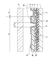
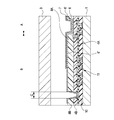
- Fig. 1 is a sectional view schematically showing an example of an organic light-emitting device according to an embodiment of the present invention.
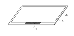
- Fig. 2 is a perspective view schematically showing an example of an organic light-emitting device according to an embodiment of the present invention.
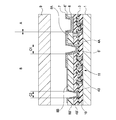
- Fig. 3 is a sectional view schematically showing an example of an organic light-emitting device according to another embodiment of the present invention.
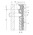
- Fig. 4 is a sectional view schematically showing an example of an organic light-emitting device according to a further embodiment of the present invention.
- Fig. 5 is a sectional view schematically showing an example of an organic light-emitting device according to a still further embodiment of the present invention.
- Fig. 1 is a sectional view schematically showing an example of an organic light-emitting device according to an embodiment of the present invention.
- Fig. 2 is a perspective view schematically showing an example of an organic light-emitting device according to an embodiment of the present invention.
- Fig. 3 is
- FIG. 6 is a sectional view schematically showing an example of an organic light-emitting device according to a further embodiment of the present invention.
- Fig. 7 is a sectional view schematically showing a comparative example of an organic light-emitting device according to an embodiment of the present invention.
- Fig. 1 is a schematic sectional view of an end portion of an organic light-emitting device according to the present invention.
- Fig. 2 is a perspective view of an organic light-emitting device according to the present invention.
- Fig. 1 is a sectional view of a boundary portion between an emission region A and a peripheral region B serving as a non-emission region disposed around the emission region A shown in Fig. 2.
- the emission region is a region in which a plurality of defined pixels are arranged, the region including a plurality of pixels and regions sandwiched between the pixels.
- Each of the pixels is a portion including a light-emitting layer held between electrodes.
- a thin film transistor (TFT) 2 an inorganic insulating film 3, and a planarization film 4A are laminated in that order on a substrate 1, a first electrode 5 of a unit pixel is formed on the planarization film 4A.
- the periphery of each pixel is covered with an element separation film 8A.
- the substrate 1 is composed of an inorganic material such as glass, Si, or the like.
- the planarization film 4A planarizes the TFT 2, and the element separation film 8A defines the pixels, both films being composed of resins.
- the resins acrylic resin, polyimide resin, or the like can be used.
- the first electrode 5 is connected to the TFT 2 through a contact hole formed in the inorganic insulating film 3 and the planarization film 4A.
- An organic compound layer 6 is formed on the first electrode 5 formed in each pixel on the substrate 1.
- the organic compound layer 6 has a light-emitting layer and a charge transport layer 6'.
- the charge transport layer 6' may include one of a hole injection layer, a hole transport layer, an electron transport layer, and an electron injection layer or may include a plurality of layers of these layer.
- a second electrode 7 is formed over the organic compound layer 6.
- a sealing glass 9 is disposed to over the whole of the emission region A, and the periphery of the sealing glass 9 is bonded to the substrate 1 with an adhesive (not shown).
- a drive circuit 1 which controls drive of the TFT 2 is provided, and a planarization film 4B and an element separation film 8B are formed on the drive circuit 11.
- the planarization film 4B and the element separation film 8B are formed integrally with the planarization film 4A and the element separation film 8A, respectively, and then partially removed from a portion around the emission region A to provide a dividing region C. That is, the planarization film and the element separation film which have high contents of moisture and gases are divided between the emission region A and the peripheral region B.
- the element separation film 8B is formed integrally with the element separation film 8A and then separated from the element separation film 8A. Therefore, the element separation film 8B has no function to define pixels and may be interpreted as a part of the planarization film 4B. However, for convenience sake, the term "the element separation film 8B" is used.
- planarization film 4A and the planarization film 4B may be formed independently so as to be separated by the dividing region C at the time of formation.
- the element separation film 8A and the element separation film 8B may be formed independently on the planarization film 4A and the planarization film 4B, respectively. Further, neither the planarization film 4B nor the element separation film 8B may be formed, or only one of both films may be formed.
- the charge transport layer 6' in each pixel is provided to extend to the outside of the emission region A so as to cover the side surface of a peripheral portion of the planarization film 4A, which is disposed in the peripheral region B, the planarization film 4A being formed in the emission region A.
- the charge transport layer 6' may be formed to cover a portion or a side of the periphery of the planarization film 4A but formed to cover the whole periphery.
- the charge transport layer 6' includes one of a hole injection layer, a hole transport layer, an electron transport layer, and an electron injection layer or combination of these layers.
- the charge transport layer 6' contains any one of alkali metals and alkaline-earth metals.
- a layer containing at least one of alkali metals and alkaline-earth metals is an electron injection layer, and the charge transport layer 6' includes at least the electron injection layer.
- the alkali metals include Li, Na, K, Rb, Cs, and Fr
- the alkaline-earth metals include Be, Mg, Ca, Sr, Ba, and Ra.
- the alkali metals and the alkaline-earth metals have high ionization tendency and thus have high reactivity with moisture and gases. Therefore, the alkali metals and the alkaline-earth metals chemically bond with moisture and gases to function as an adsorbent.
- moisture and gases remaining in the planarization film 4A and the element separation film 8A are adsorbed by the charge transport layer 6' which covers the side surfaces of the peripheral portions of the planarization film 4A and the element separation film 8A, which are disposed in the peripheral region B. That is, a portion of the charge transport layer 6' which is disposed outside a pixel and the emission region A functions as an adsorbent for moisture and gases.
- the planarization film 4A and the element separation film 8A are not exposed, and thus if moisture and gases are present in the sealing space, entering of moisture and gases into the planarization film 4A and the element separation film 8A can be decreased.
- the charge transport layer 6' is formed to cover not only the element separation film 8A but also the planarization film 4A. Therefore, moisture and gases remaining in the planarization film 4A and the element separation film 8A diffuse therein and are efficiently adsorbed by the charge transport layer 6'.
- the present invention has the configuration in which the charge transport layer 6' containing any one of alkali metals and alkaline-earth metals is provided to extend to the outside of the emission region A so as to cover the side surfaces of peripheral portions of the planarization film 4A and the element separation film 8A, which are disposed in the peripheral region B, the planarization film 4A and the element separation film 8A being formed in the emission region A.
- alkali metals and alkaline-earth metals are not limited as long as they have adsorptivity for moisture and gases.
- Li, Na, Cs, Mg, Ca, Sr, and compounds thereof can be used.
- the charge transport layer 6' is formed to extent across the dividing region C and cover the side surfaces of portions of the planarization film 4B and the element separation film 8B, which are disposed in the dividing region C, the planarization film 4B and the element separation film 8B being formed in the peripheral region B.
- moisture and gases remaining in the planarization film 4B and the element separation film 8B are adsorbed by the charge transport layer 6', thereby decreasing the amount of moisture and gases released from the planarization film 4B and the element separation film 8B to the sealing space.
- the area of the planarization film 4B and the element separation film 8B covered with the charge transport layer 6' may be increased.
- electrode wiring 10 is formed over the planarization film 4B and the element separation film 8B, for supplying a potential to a second electrode. Therefore, in order to electrically connect the second electrode and the electrode wiring, the charge transport layer 6' is formed so as not to be disposed on the electrode wiring 10.
- a dividing region C2 is provided at a position opposite to the emission region A with respect to the dividing region C1.
- the planarization film 4B and the element separation film 8B in the peripheral region B are divided into planarization film 4B and element separation film 8B which cover the drive circuit 11 and other planarization film 4B' and element separation film 8B'.
- the electrode wiring 10 is provided in the dividing region C2, and the electrode wiring 10 is electrically connected to the second electrode 7 through a contact hole formed in an inorganic insulating film 3. In this configuration, the electrode wiring 10 can be formed at the same time as the step of forming the TFT 2 and the drive circuit 11.
- the electrode wiring 10 is provided in a dividing region C, and the second electrode 7 is electrically connected to the electrode wiring 10 in the dividing region C.
- the electrode wiring 10 is provided near the emission region A where pixels are formed, and thus reduction of a potential to be supplied to the second electrode 7 in each pixel can be suppressed.
- the charge transport layer 6' is formed to extent to the outside of the emission region A so as to cover the side surface of a peripheral portion of the planarization film 4A, which is disposed in the peripheral region B. Therefore, this embodiment has the advantage of the present invention.
- a further embodiment shown in Fig. 5 has a configuration in which the planarization film 4B and the element separation film 8B are not formed in the peripheral region B. In this configuration, the amount of moisture and gases remaining in the light-emitting device can be decreased.
- the electrode wiring 10 is disposed outside of the driving circuit 11 in the light-emitting device, the electrode wiring 10 may be disposed between the driving circuit 11 and the emission region A. In this case, in order to electrically connect the second electrode 7 and the electrode wiring 10, the charge transport layer 6' is formed so as not to be disposed on the electrode wiring 10.
- the sealing glass 9 is used as the sealing layer
- the sealing layer is not particularly limited as long as it can prevent entering of atmospheric moisture and gases into the light-emitting device.
- an inorganic sealing film composed of an inorganic material, for example, silicon nitride, silicon oxide, or the like, may be formed as the sealing layer on the second electrode 7, and a polarization plate may be bonded through an adhesive layer.
- the charge transport layer 6' is formed to extent to the outside of the emission region A so as to cover the side surface of a peripheral portion of the planarization film 4A, which is disposed in the peripheral region B. Therefore, this embodiment has the advantage of the present invention.
- moisture and gases remaining in the planarization film 4B and the element separation film 8B are adsorbed by the charge transport layer 6' provided in contact with the planarization film 4B and the element separation film 8B.
- the charge transport layer 6' contains Li
- moisture and gases remaining in the planarization film 4B and the element separation film 8B are adsorbed by chemical bonding.
- chemical bonding between the adsorbed moisture and gases and Li may be broken and moisture and gases may diffuse into an organic EL element in each pixel within the emission region A through the charge transport layer 6' or the interface between the charge transport layer 6' and the second electrode 7.
- a structure 13 is formed along a dividing region C in the dividing region C.
- the charge transport layer 6' is divided by the structure 13 and becomes discontinued, and the structure 13 is in contact with the second electrode 7.
- the structure can be formed using an inorganic material which little adsorbs moisture and gases.
- the shape of the structure 13 is not limited as long as the condition of contact between the structure 13 and the second electrode 7 is satisfied in the process of forming the charge transport layer 6' and the second electrode 7.
- the taper angle of the side wall of the structure 13 is 45 degrees (angle) or more, particularly over 80 degrees (angle).
- the layer constituting the charge transport layer 6' is formed by an evaporation process with high linearity, an organic material which constitutes the charge transport layer 6' little moves toward the side wall of the structure 13 disposed in the dividing region C, and thus the charge transport layer 6' does not cover the whole side wall of the structure 13.
- the second electrode 7 is formed by sputtering, a material of the second electrode 7 moves toward the side wall of the structure, and thus the second electrode 7 is formed over the whole side wall of the structure 13, continuously forming the second electrode 7 on the side wall of the structure 13. Therefore, the charge transport layer 6' is divided by the structure 13 in the dividing region C and becomes discontinued.
- the structure 13 When the structure 13 is formed using a conductive material, electric connection can be made between the structure 13 and the second electrode 7, and the structure 13 can be used as potential wiring for the second electrode 7.
- the potential wiring is provided for compensating a potential corresponding to a voltage drop produced when a potential is supplied to a pixel through the electrode wiring 10.
- the structure 13 is preferably made of a conductive material and more preferably a conductive material with low resistance.
- a single layer film composed of Al, Mo, Ag, Cu, or a compound thereof, or a laminated film containing these materials can be used.
- the same material as that for forming each layer of the TFT 2 and the first electrode 5 can be used.
- the structure 13 can be formed along the dividing region C in the dividing region C, but the structure 13 may be provided in the emission region A or the peripheral region B so that the charge transport layer 6' is discontinued in the horizontal direction of the drawing.
- Fig. 6 illustrates one structure 13, but two structures may be arranged in parallel along the dividing region under conditions satisfying the above-described taper angle.
- the charge transport layer 6' may be discontinued by forming the inorganic insulating film 3 so that the inorganic insulating film 3 is not formed in a portion where the dividing region C to be formed.
- the TFT 2 was formed in the emission region A of the substrate 1 having the emission region A and the peripheral region B, and the drive circuit 11 for controlling drive of the TFT 2 was formed on the peripheral region B.
- the electrode wiring 10 was formed on the peripheral region B at the same time as the formation of drain wiring of the TFT 2.
- the inorganic insulating film 3 was formed on the TFT 2 and the drive circuit 11 so as not to cover the electrode wiring 10.
- the planarization film 4A was formed in the emission region A
- the planarization film 4B was formed in the peripheral region B so as to be separated from the planarization film 4A by the dividing region C and to surround the emission region A.
- the planarization film 4A and the planarization film 4B were made of acrylic resin.
- the electrode wiring 10 was not covered with the planarization film 4B.
- a contact hole was formed in the planarization film 4A in order to make electric contact between the first electrode 5 and the TFT 2, and the first electrode 5 was formed on the planarization film 4A.
- the acrylic element separation film 8A was formed around the first electrode 5 on the planarization film 4A to define pixels.
- the acrylic element separation film 8B was formed on the planarization film 4B so that the planarization film 4B and the element separation film 8B were separated from the planarization film 4A and the element separation film 8A by the dividing region C so as to surround the emission region A.
- planarization film 4B and the element separation film 8B were formed to surround the emission region A, the planarization film 4B and the element separation film 8B need not surround the emission region A as long as they are provided to cover at least the drive circuit 11. Further, any one of the planarization film 4B and the element separation film 8B may be omitted or both films may be omitted.
- tungsten As a material of the first electrode 5, tungsten was used. Further, in order to increase emission efficiency, a reflecting layer for reflecting light emitted in the direction to the substrate 1 so that the light is taken from the sealing glass 9 side, and a hole injection layer may be laminated on the first electrode 5.
- a material for the reflecting layer a material with high reflectivity, for example, an Ag alloy, an Al alloy, or the like, can be used. In this example, an Ag alloy was used.
- the hole injection layer is not particularly limited as long energy level connection to a hole transport layer is taken into consideration, and ITO, IZO, or the like can be used. In this example, ITO was used.
- the thickness of the planarization film 4A and the planarization film 4B was 2 micrometers, and the thickness of the element separation film 8A and the element separation film 8B was 1.5 micrometers.
- the size of apertures for defining the pixels was 30 micrometers * 45 micrometers, and the width between the pixels was 15 micrometers.
- the width of the dividing region C was 100 micrometers, and the electrode wiring 10 was formed at a distance of 350 micrometers from the dividing region C.
- FLO3, DpyFL + sDTAB2, DFPH1, and DFPH1 + Cs2CO3 were deposited by evaporation to form organic compound layers 6 including a hole transport layer, a light emitting layer, an electron transport layer, and an electron injection layer.
- charge transport layers 6' including three layers, i.e., a hole transport layer (FLO3), an electron transport layer (DFPH1), and an electron injection layer (DFPH1 + Cs2CO3), were formed to cross the dividing region C and extend from the first electrode 5 of each pixel to a portion of the top of the element separation film 8.
- the charge transport layers 6' covered 150 micrometers of the top of the element separation film 8 in the peripheral region B.
- the charge transport layers 6' were not disposed on the electrode wiring 10. Then, the second electrode 7 composed of IZO was deposited to a thickness of 0.04 micrometer on the organic compound layers 6 in each pixel, the charge transport layers 6' extending to outside of the emission region A, and the electrode wiring 10 to form an organic EL element in each pixel.
- the sealing glass 9 on which a desiccant (not shown) was disposed was bonded so that the sealing glass 9 faced the substrate 1 and sealed to form an organic EL light-emitting element shown in Fig. 3.
- the operations up to the formation of the second electrode 7 were performed in vacuum, and then the sealing work was performed in an atmosphere filled with nitrogen and controlled to a dew point of -75 degrees (Celsius) or less.
- the organic light-emitting device of this example was stored in an environmental chamber controlled to a temperature of 80 degrees (Celsius) and a humidity of 25% or less. Emission display was performed at an interval of predetermined time, and the emission state of each pixel in the emission region A was observed with a microscope at a magnification of 500 times. After 3000 hours elapsed, deterioration was confirmed, in which the pixel emission area decreased at the four corners of the emission region A. The deterioration occurred in 6 pixels or less from the periphery of the emission region A. In the other portions of the emission region, visible deterioration of emission was not observed, and quality of a displayed image was maintained at a level equivalent to that before temperature loading.
- the charge transport layers 6' include the three layers, i.e., the hole transport layer, the electron transport layer, and the electron injection layer.
- the effect of the present invention is exhibited as long as the charge transport layers 6' include at least the electron injection layer containing Cs as an alkali metal.
- the same organic light-emitting device as Example 1 was produced except that the electrode wiring is formed on the planarization film 4B and the element separation film 8B which are formed in the peripheral region B, and the structure 13 is formed in the dividing region C when the first electrode 5 is formed.
- the electrode wiring 10 was formed after the element separation film 8B was formed and before the charge transport layers 6' including the three layers, i.e., the hole transport layer, the electron transport layer, and the electron injection layer, were formed by evaporation.
- the structure 13 was formed along the dividing region C in the dividing region C at the same time as the formation of the first electrode 5.
- the structure 13 had a width of 30 micrometers and a height of 0.25 micrometer.
- the total thickness of the charge transport layers 6' was 0.11 micrometer, and each of the layers of the charge transport layers 6' was formed by an evaporation process causing little deviation. Therefore, the charge transport layers 6' were divided by the structure 13 within the dividing region C. Further, the second electrode 7 was deposited on the organic compound layers 6 and the charge transport layers 6' by a sputtering process. Since the sputtering process caused wraparound, the second electrode 7 was formed on the side surfaces of the structure 13, and thus the second electrode 7 was not divided by the structure 13 and not discontinuous.
- the organic light-emitting device of this example was stored in an environmental chamber controlled to a temperature of 80 degrees (Celsius) and a humidity of 25% or less. Emission display was performed at an interval of predetermined time, and the emission state of each pixel in the emission region A was observed with a microscope at a magnification of 500 times. After 3000 hours elapsed, deterioration was confirmed, in which the pixel emission area decreased at the four corners of the emission region A. The deterioration occurred in 2 pixels or less from the periphery of the emission region A. In the other portions of the emission region, visible deterioration of emission was not observed, and quality of a displayed image was maintained at a level equivalent to that before temperature loading.
- Example 3 the same organic light-emitting device as Example 1 was produced except that the dividing region C1 (Fig. 3) was not formed, only the dividing region C2 was formed, and the charge transport layers 6' did not cover the side surface of a peripheral portion of the planarization film 4A which is disposed in the peripheral region B, the planarization film 4A being formed in the emission region A.
- the dividing region C1 Fig. 3
- the charge transport layers 6' did not cover the side surface of a peripheral portion of the planarization film 4A which is disposed in the peripheral region B, the planarization film 4A being formed in the emission region A.
- the organic light-emitting device of this comparative example was stored in an environmental chamber controlled to a temperature of 80 degrees (Celsius) and a humidity of 25% or less. Emission display was performed at an interval of predetermined time, and the emission state of each pixel in the emission region A was observed with a microscope at a magnification of 500 times. After 800 hours elapsed, deterioration was confirmed, in which the pixel emission area decreased at the four corners of the emission region A. The deterioration occurred in 6 pixels or less from the periphery of the emission region A.
- the charge transport layer containing any one of alkali metals and alkaline earth metals are adsorbed by the charge transport layer containing any one of alkali metals and alkaline earth metals, thereby decreasing the amounts of moisture and gases diffusing into an organic EL element in each pixel.
- the charge transport layer provided in each pixel is extended to cover the side surface of a peripheral portion of the planarization film, which is disposed in the peripheral region, avoiding the planarization film and the element separation film in the emission region from being exposed to the sealing space. Therefore, even if moisture and gases are present in the sealing space, entering of the moisture and gases into the planarization film and the element separation film can be decreased.
- planarization film and the element separation film are covered with the charge transport layer, moisture and gases remaining in the planarization film and the element separation film can be efficiently adsorbed by the charge transport layer. As a result, an organic light-emitting device with excellent long-term reliability can be provided.
- Substrate 2 Thin film transistor (TFT) 3 Inorganic insulating film 4A, 4B, 4B' Planarization film 5 First electrode 6 Organic compound layer 6' Charge transport layer 7 Second electrode 8A, 8B, 8B' Element separation film 9 Sealing glass 10 Electrode wiring 11 Drive circuit 12 Power supply and signal supply pad 13 Structure A Emission region B Peripheral region C, C1, C2 Dividing region
Landscapes
- Physics & Mathematics (AREA)
- Optics & Photonics (AREA)
- Engineering & Computer Science (AREA)
- Microelectronics & Electronic Packaging (AREA)
- Electroluminescent Light Sources (AREA)
Abstract
Description
An organic light-emitting device of the present invention has a substrate having an emission region in which pixels are arranged and a peripheral region which surrounds the emission region, thin film transistors arranged in the emission region of the substrate, a planarization film composed of a resin which planarizes the thin film transistors, an element separation film which defines pixels formed on the planarization film, and an organic EL element including at least a first electrode, a light-emitting layer, a charge transport layer comprising any one of alkali metals and alkaline-earth metals, and a second electrode, which are disposed on the planarization film within each of the pixels, wherein the charge transport layer extends to outside of the emission region so as to cover the side surface of a peripheral portion of the planarization film, which is disposed in the peripheral region, the planarization film being formed in the emission region.
2 Thin film transistor (TFT)
3 Inorganic insulating film
4A, 4B, 4B' Planarization film
5 First electrode
6 Organic compound layer
6' Charge transport layer
7 Second electrode
8A, 8B, 8B' Element separation film
9 Sealing glass
10 Electrode wiring
11 Drive circuit
12 Power supply and signal supply pad
13 Structure
A Emission region
B Peripheral region
C, C1, C2 Dividing region
Claims (6)
- An organic light-emitting device comprising:
a substrate having an emission region in which pixels are arranged and a peripheral region which surrounds the emission region,
thin film transistors arranged in the emission region of the substrate,
a planarization film which is composed of a resin and which planarizes the thin film transistors,
an element separation film which defines pixels formed on the planarization film, and
an organic EL element including at least a first electrode, a light-emitting layer, a charge transport layer containing any one of alkali metals and alkaline-earth metals, and a second electrode, which are disposed on the planarization film within each of the pixels,
wherein the charge transport layer extends to outside of the emission region so as to cover the side surface of a peripheral portion of the planarization film, which is disposed in the peripheral region, the planarization film being formed in the emission region. - The organic light-emitting device according to Claim 1, wherein the charge transport layer is in contact with the element separation film and/or the planarization film.
- The organic light-emitting device according to Claim 1, wherein a drive circuit is disposed in the peripheral region of the substrate in order to control drive of the thin film transistors, the planarization film is formed on the drive circuit, and the planarization film is divided by a dividing region provided in the peripheral region.
- The organic light-emitting device according to Claim 3, wherein the charge transport layer extends to the peripheral region so as to cover the dividing region of the substrate and a side surface of the planarization film on the drive circuit, the side surface being disposed in the dividing region.
- The organic light-emitting device according to Claim 4, wherein the charge transport layer is discontinued in the dividing region by a structure formed along the dividing region within the dividing region of the substrate.
- The organic light-emitting device according to Claim 5, wherein the structure is composed of a conductive material and is electrically connected to the second electrode.
Priority Applications (2)
| Application Number | Priority Date | Filing Date | Title |
|---|---|---|---|
| US12/996,732 US8766241B2 (en) | 2008-06-09 | 2009-06-04 | Organic light-emitting device |
| CN2009801210343A CN102057513B (en) | 2008-06-09 | 2009-06-04 | Organic light-emitting device |
Applications Claiming Priority (2)
| Application Number | Priority Date | Filing Date | Title |
|---|---|---|---|
| JP2008-150489 | 2008-06-09 | ||
| JP2008150489A JP4991634B2 (en) | 2008-06-09 | 2008-06-09 | Organic EL light emitting device |
Publications (1)
| Publication Number | Publication Date |
|---|---|
| WO2009150802A1 true WO2009150802A1 (en) | 2009-12-17 |
Family
ID=41416515
Family Applications (1)
| Application Number | Title | Priority Date | Filing Date |
|---|---|---|---|
| PCT/JP2009/002520 Ceased WO2009150802A1 (en) | 2008-06-09 | 2009-06-04 | Organic light-emitting device |
Country Status (5)
| Country | Link |
|---|---|
| US (1) | US8766241B2 (en) |
| JP (1) | JP4991634B2 (en) |
| KR (1) | KR20110025956A (en) |
| CN (1) | CN102057513B (en) |
| WO (1) | WO2009150802A1 (en) |
Cited By (2)
| Publication number | Priority date | Publication date | Assignee | Title |
|---|---|---|---|---|
| EP3327816A1 (en) * | 2016-11-28 | 2018-05-30 | LG Display Co., Ltd. | Lighting apparatus using organic light emitting device and method of fabricating thereof |
| GB2602721A (en) * | 2020-12-31 | 2022-07-13 | Lg Display Co Ltd | Light emitting display device |
Families Citing this family (25)
| Publication number | Priority date | Publication date | Assignee | Title |
|---|---|---|---|---|
| JP5183716B2 (en) * | 2009-12-21 | 2013-04-17 | キヤノン株式会社 | Light emitting device |
| KR20130007053A (en) * | 2011-06-28 | 2013-01-18 | 삼성디스플레이 주식회사 | Organinc light emitting display device and manufacturing method for the same |
| KR101521676B1 (en) * | 2011-09-20 | 2015-05-19 | 엘지디스플레이 주식회사 | Organic light emitting diode display and method for manufacturing the same |
| KR101994227B1 (en) * | 2012-12-07 | 2019-09-30 | 엘지디스플레이 주식회사 | Organic light emitting diode device and method for fabricating the same |
| KR102132882B1 (en) | 2012-12-20 | 2020-07-13 | 삼성디스플레이 주식회사 | Thin film transistor substrate, organic light emitting apparatus comprising the same, method for manufacturing thin film transistor substrate, and method for manufacturing organic light emitting apparatus |
| JP6074597B2 (en) * | 2013-03-29 | 2017-02-08 | 株式会社Joled | Organic EL display device and electronic device |
| KR102079253B1 (en) | 2013-06-26 | 2020-02-20 | 삼성디스플레이 주식회사 | Thin film transistor substrate, organic light emitting apparatus comprising the same, method for manufacturing thin film transistor substrate, and method for manufacturing organic light emitting apparatus |
| JP6391917B2 (en) | 2013-07-03 | 2018-09-19 | 株式会社ジャパンディスプレイ | Light emitting element display device and manufacturing method thereof |
| JP6329795B2 (en) * | 2014-03-27 | 2018-05-23 | 株式会社ジャパンディスプレイ | EL display device and method of manufacturing EL display device |
| JP6306402B2 (en) | 2014-04-08 | 2018-04-04 | 株式会社ジャパンディスプレイ | Organic EL display device and method of manufacturing organic EL display device |
| JP6634290B2 (en) | 2016-01-04 | 2020-01-22 | 株式会社ジャパンディスプレイ | Organic EL display |
| KR102598926B1 (en) * | 2016-10-31 | 2023-11-03 | 엘지디스플레이 주식회사 | Lighting apparatus using organic light emitting device and method of fabricating thereof |
| KR102582059B1 (en) * | 2016-12-30 | 2023-09-21 | 엘지디스플레이 주식회사 | Display apparatus and multi screen display apparatus using the same |
| CN106876331B (en) * | 2017-03-03 | 2019-11-22 | 武汉华星光电技术有限公司 | OLED display panel, manufacturing method thereof, and display device |
| JP6912080B2 (en) * | 2017-06-09 | 2021-07-28 | 株式会社Joled | Organic EL display panel |
| JP6742277B2 (en) * | 2017-07-03 | 2020-08-19 | 株式会社Joled | Display device and method of manufacturing display device |
| KR102429676B1 (en) * | 2017-10-27 | 2022-08-05 | 엘지디스플레이 주식회사 | Display device |
| CN111903187B (en) * | 2018-03-28 | 2023-07-04 | 夏普株式会社 | display device |
| US12207503B2 (en) * | 2018-09-28 | 2025-01-21 | Sharp Kabushiki Kaisha | Display device |
| CN110993814B (en) | 2019-11-15 | 2021-09-03 | 深圳市华星光电半导体显示技术有限公司 | Display device and method for manufacturing the same |
| KR20210086059A (en) * | 2019-12-31 | 2021-07-08 | 엘지디스플레이 주식회사 | Display device and manufacturing method thereof |
| KR20220020166A (en) * | 2020-08-11 | 2022-02-18 | 엘지디스플레이 주식회사 | Display apparatus |
| KR20230103694A (en) * | 2021-12-31 | 2023-07-07 | 엘지디스플레이 주식회사 | Light Emitting Display Device |
| CN117716808B (en) * | 2022-05-27 | 2025-07-18 | 京东方科技集团股份有限公司 | Display panel and display device |
| KR20240025337A (en) * | 2022-08-18 | 2024-02-27 | 엘지디스플레이 주식회사 | Display device |
Citations (6)
| Publication number | Priority date | Publication date | Assignee | Title |
|---|---|---|---|---|
| US20050023964A1 (en) * | 2003-05-08 | 2005-02-03 | Sanyo Electric Co., Ltd. | Organic EL display device |
| JP2005164818A (en) * | 2003-12-01 | 2005-06-23 | Mitsubishi Electric Corp | Display device |
| US20050218396A1 (en) * | 2004-03-16 | 2005-10-06 | Semiconductor Energy Laboratory Co., Ltd. | Display device |
| US20060033429A1 (en) * | 2004-08-12 | 2006-02-16 | Hiroshi Fujimura | Display device |
| US20070228380A1 (en) * | 2006-03-29 | 2007-10-04 | Canon Kabushiki Kaisha | Organic light-emitting device |
| US20090101904A1 (en) * | 2007-10-19 | 2009-04-23 | Sony Corporation | Display device |
Family Cites Families (7)
| Publication number | Priority date | Publication date | Assignee | Title |
|---|---|---|---|---|
| US6306694B1 (en) * | 1999-03-12 | 2001-10-23 | Semiconductor Energy Laboratory Co., Ltd. | Process of fabricating a semiconductor device |
| US6531713B1 (en) * | 1999-03-19 | 2003-03-11 | Semiconductor Energy Laboratory Co., Ltd. | Electro-optical device and manufacturing method thereof |
| US7122835B1 (en) * | 1999-04-07 | 2006-10-17 | Semiconductor Energy Laboratory Co., Ltd. | Electrooptical device and a method of manufacturing the same |
| TW444257B (en) * | 1999-04-12 | 2001-07-01 | Semiconductor Energy Lab | Semiconductor device and method for fabricating the same |
| US6524877B1 (en) * | 1999-10-26 | 2003-02-25 | Semiconductor Energy Laboratory Co., Ltd. | Semiconductor device, and method of fabricating the same |
| DE10338550A1 (en) * | 2003-08-19 | 2005-03-31 | Basf Ag | Transition metal complexes with carbene ligands as emitters for organic light-emitting diodes (OLEDs) |
| JP4776949B2 (en) * | 2004-03-16 | 2011-09-21 | 株式会社半導体エネルギー研究所 | Light emitting device |
-
2008
- 2008-06-09 JP JP2008150489A patent/JP4991634B2/en not_active Expired - Fee Related
-
2009
- 2009-06-04 US US12/996,732 patent/US8766241B2/en not_active Expired - Fee Related
- 2009-06-04 KR KR1020117000267A patent/KR20110025956A/en not_active Ceased
- 2009-06-04 WO PCT/JP2009/002520 patent/WO2009150802A1/en not_active Ceased
- 2009-06-04 CN CN2009801210343A patent/CN102057513B/en not_active Expired - Fee Related
Patent Citations (6)
| Publication number | Priority date | Publication date | Assignee | Title |
|---|---|---|---|---|
| US20050023964A1 (en) * | 2003-05-08 | 2005-02-03 | Sanyo Electric Co., Ltd. | Organic EL display device |
| JP2005164818A (en) * | 2003-12-01 | 2005-06-23 | Mitsubishi Electric Corp | Display device |
| US20050218396A1 (en) * | 2004-03-16 | 2005-10-06 | Semiconductor Energy Laboratory Co., Ltd. | Display device |
| US20060033429A1 (en) * | 2004-08-12 | 2006-02-16 | Hiroshi Fujimura | Display device |
| US20070228380A1 (en) * | 2006-03-29 | 2007-10-04 | Canon Kabushiki Kaisha | Organic light-emitting device |
| US20090101904A1 (en) * | 2007-10-19 | 2009-04-23 | Sony Corporation | Display device |
Cited By (4)
| Publication number | Priority date | Publication date | Assignee | Title |
|---|---|---|---|---|
| EP3327816A1 (en) * | 2016-11-28 | 2018-05-30 | LG Display Co., Ltd. | Lighting apparatus using organic light emitting device and method of fabricating thereof |
| GB2602721A (en) * | 2020-12-31 | 2022-07-13 | Lg Display Co Ltd | Light emitting display device |
| US11839127B2 (en) | 2020-12-31 | 2023-12-05 | Lg Display Co., Ltd. | Light emitting display device with electron injection layer at non-active area |
| GB2602721B (en) * | 2020-12-31 | 2024-06-12 | Lg Display Co Ltd | Light emitting display device |
Also Published As
| Publication number | Publication date |
|---|---|
| US20110163331A1 (en) | 2011-07-07 |
| US8766241B2 (en) | 2014-07-01 |
| CN102057513A (en) | 2011-05-11 |
| JP4991634B2 (en) | 2012-08-01 |
| KR20110025956A (en) | 2011-03-14 |
| CN102057513B (en) | 2013-06-05 |
| JP2009295911A (en) | 2009-12-17 |
Similar Documents
| Publication | Publication Date | Title |
|---|---|---|
| US8766241B2 (en) | Organic light-emitting device | |
| EP1648032B1 (en) | Organic electro luminescence device and fabrication method thereof | |
| EP2190021B1 (en) | Organic electroluminescent display device | |
| US9831299B2 (en) | OLED display panel and manufacturing method thereof | |
| US20110221334A1 (en) | Organic light emitting diode display | |
| US9425251B2 (en) | Thin film transistor substrate and organic light-emitting diode (OLED) display having the same | |
| JP2006156035A (en) | Display device | |
| KR20150059478A (en) | Organic electro luminescent device | |
| US7872255B2 (en) | Organic light-emitting device | |
| JP2008058928A (en) | Organic light emitting display | |
| US7049744B2 (en) | Organic electroluminescence panel having a substrate and a sealing panel sealed by adhering an inorganic film and the sealing panel using a sealing material | |
| KR100710170B1 (en) | Organic EL device and method of manufacturing the same | |
| JP4094280B2 (en) | Electroluminescent display device | |
| KR20150000571A (en) | Organic light emitting diode display device | |
| KR20050066569A (en) | Dual panel type organic electroluminescent device and method for fabricating the same | |
| KR100518962B1 (en) | Organic Electroluminescent Device | |
| KR100557237B1 (en) | Dual panel type organic electroluminescent device and manufacturing method thereof | |
| US20080259549A1 (en) | Display device | |
| KR100616706B1 (en) | Organic electroluminescent device and manufacturing method thereof | |
| KR102689907B1 (en) | Display apparatus | |
| CN110072309B (en) | light-emitting device | |
| KR20050066571A (en) | Dual panel type organic electroluminescent device and method for fabricating the same | |
| KR20050104100A (en) | Organic electro luminescence device and fabrication method thereof | |
| KR101918814B1 (en) | Three dimensional organic light emitting display device and method of manufacturing the same | |
| KR20240094733A (en) | Encapsulation element and display device |
Legal Events
| Date | Code | Title | Description |
|---|---|---|---|
| WWE | Wipo information: entry into national phase |
Ref document number: 200980121034.3 Country of ref document: CN |
|
| 121 | Ep: the epo has been informed by wipo that ep was designated in this application |
Ref document number: 09762233 Country of ref document: EP Kind code of ref document: A1 |
|
| NENP | Non-entry into the national phase |
Ref country code: DE |
|
| ENP | Entry into the national phase |
Ref document number: 20117000267 Country of ref document: KR Kind code of ref document: A |
|
| WWE | Wipo information: entry into national phase |
Ref document number: 12996732 Country of ref document: US |
|
| 122 | Ep: pct application non-entry in european phase |
Ref document number: 09762233 Country of ref document: EP Kind code of ref document: A1 |