WO2009144878A1 - Sensor and method for manufacturing the same - Google Patents
Sensor and method for manufacturing the same Download PDFInfo
- Publication number
- WO2009144878A1 WO2009144878A1 PCT/JP2009/002092 JP2009002092W WO2009144878A1 WO 2009144878 A1 WO2009144878 A1 WO 2009144878A1 JP 2009002092 W JP2009002092 W JP 2009002092W WO 2009144878 A1 WO2009144878 A1 WO 2009144878A1
- Authority
- WO
- WIPO (PCT)
- Prior art keywords
- oxide film
- silicon oxide
- reaction field
- sensor
- channel
- Prior art date
Links
Images


Classifications
-
- G—PHYSICS
- G01—MEASURING; TESTING
- G01N—INVESTIGATING OR ANALYSING MATERIALS BY DETERMINING THEIR CHEMICAL OR PHYSICAL PROPERTIES
- G01N27/00—Investigating or analysing materials by the use of electric, electrochemical, or magnetic means
- G01N27/26—Investigating or analysing materials by the use of electric, electrochemical, or magnetic means by investigating electrochemical variables; by using electrolysis or electrophoresis
- G01N27/403—Cells and electrode assemblies
- G01N27/414—Ion-sensitive or chemical field-effect transistors, i.e. ISFETS or CHEMFETS
- G01N27/4145—Ion-sensitive or chemical field-effect transistors, i.e. ISFETS or CHEMFETS specially adapted for biomolecules, e.g. gate electrode with immobilised receptors
Definitions
- the present invention relates to a sensor used as, for example, a biosensor or a pH sensor and a manufacturing method thereof, and more particularly to a sensor including a FET (Field Effect Transistor) and a manufacturing method thereof.
- a sensor used as, for example, a biosensor or a pH sensor and a manufacturing method thereof, and more particularly to a sensor including a FET (Field Effect Transistor) and a manufacturing method thereof.
- FET Field Effect Transistor
- sensors such as biosensors and pH sensors using FETs have been proposed (see Patent Documents 1 to 3).
- a source electrode and a drain electrode are electrically connected by a channel formed on an insulating film.
- a reaction field for the substance to be detected is formed on the channel.
- the reaction field is provided with a reaction membrane for immobilizing the substance to be detected.
- the gate voltage is applied from above the reaction film by the gate electrode, and the source-drain current at that time is measured to measure the concentration of the substance to be detected provided in the reaction field.
- the channel functions as a sensing unit. Therefore, the amount of change in source-drain current with respect to the gate voltage (that is, measurement sensitivity) varies depending on the shape of the channel. Therefore, it is desirable that the shape of the channel can be freely selected according to the type of the detection object to be measured.
- the area of the reaction field also affects the potential applied to the FET substrate from the substance to be detected. Therefore, the measurement sensitivity varies depending on the area of the reaction field. Therefore, it is desirable that the area of the reaction field can also be freely selected according to the type of the object to be detected. Further, the position of the reaction field is preferably wider when considering user convenience, layout as a sensor, and the like.
- the present invention provides a sensor having a high measurement sensitivity and a high degree of freedom in layout, and a manufacturing method thereof, by reducing restrictions on the shape of the channel, the area and position of the reaction field.
- the first of the present invention comprises a silicon substrate having a silicon oxide film, a source electrode, a drain electrode and a gate electrode disposed on the silicon oxide film, and polysilicon or amorphous silicon, and is disposed on the silicon oxide film,
- the present invention relates to a sensor including a channel electrically connected to the source electrode and the drain electrode, and a reaction field disposed on the silicon oxide film.
- a second aspect of the present invention includes a semiconductor substrate, a silicon oxide film formed on the surface of the semiconductor substrate, and an electrode connected to the silicon oxide film, and a part of the silicon oxide film is an object to be detected.
- the present invention relates to a manufacturing method including a step of forming and a step of forming a reaction field in the silicon oxide film.
- the reaction field is arranged on a silicon oxide film different from the channel, restrictions on the shape of the channel, the area and position of the reaction field are reduced, and the measurement sensitivity and the freedom of layout are increased. Can do.
- the channel is formed of polysilicon or amorphous silicon, a silicon oxide film, a drain electrode, a source electrode, and a channel can be easily formed using a semiconductor manufacturing process similar to that for manufacturing a TFT. The channel width and silicon oxide film thickness can also be easily selected. As a result, the measurement sensitivity can be easily changed.
- FIG. 1 The perspective view which shows typically the structure of the sensor which concerns on Embodiment 1 of this invention.
- Sectional drawing which shows the structure of the sensor which concerns on the said Embodiment 1 typically The figure which shows the relationship between the line width of the channel of the sensor which concerns on the said Embodiment 1, and measurement sensitivity The figure which shows the relationship between the thickness of the silicon oxide film of the sensor which concerns on the said Embodiment 1, and measurement sensitivity.
- Semiconductor manufacturing process of the sensor according to the first embodiment Sectional drawing which shows typically the structure of the sensor which concerns on Embodiment 2 of this invention.
- the perspective view which shows typically the structure of the sensor which concerns on Embodiment 3 of this invention.
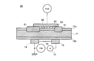
- FIG. 1 is a perspective view schematically showing a configuration of a sensor according to Embodiment 1 of the present invention.
- FIG. 2 is a cross-sectional view schematically showing the configuration of the sensor.
- This embodiment is an example in which the sensor of the present invention is applied to a biosensor, a pH sensor, or the like.
- silicon oxide films 12a and 12b which are insulating films, are formed on both surfaces of a silicon substrate 11.
- a gate electrode 13 is formed on the surface on which the silicon oxide film 12a is formed.
- a reference voltage Vref is applied to the gate electrode 13.
- the gate electrode 13, the silicon oxide film 12a, and the silicon substrate 11 have a metal-insulator-semiconductor (MIS) structure. Therefore, the gate voltage is not directly applied to the silicon substrate 11.
- the material of the gate electrode 13 is not particularly limited as long as it has conductivity. For example, a metal such as gold, platinum, titanium, and aluminum, or a conductive plastic may be used.
- drain electrode 14 and the source electrode 15 are formed on the surface on which the silicon oxide film 12b is formed.
- the drain electrode 14 and the source electrode 15 are electrically connected through the channel 16 on the silicon oxide film 12b.
- the channel 16 is made of polysilicon.
- the silicon oxide film 12b, the drain electrode 14, the source electrode 15 and the channel 16 have a general TFT (Thin-Film-Transistor) structure. Therefore, the same semiconductor manufacturing process as that used to manufacture the TFT is used.
- the silicon oxide film 12b, the drain electrode 14, the source electrode 15 and the channel 16 can be easily formed.
- the channel 16 is formed of polysilicon, the line width W of the channel 16 can be easily selected in the semiconductor manufacturing process as compared with the case where the channel 16 is formed of carbon nanotubes or the like. Become.
- a power source Vds and an ammeter 17 are connected between the drain electrode 14 and the source electrode 15 via an external wiring. Thereby, a predetermined voltage is applied between the drain electrode 14 and the source electrode 15 by the power source Vds, and the current flowing through the silicon substrate 11 is measured by the ammeter 17.
- the distance between the drain electrode 14 and the source electrode 15 is not particularly limited, but is usually about 0.5 to 10 [ ⁇ m]. This spacing may be further reduced to facilitate connection between the electrodes by the channel 16.
- the shape and size of the source electrode and the drain electrode are not particularly limited, and may be set as appropriate according to the purpose.
- a reaction field 20 is formed on the surface on which the silicon oxide film 12a is formed.
- the reaction field 20 means a region that provides a sample solution.
- the reaction field 20 and the gate electrode 13 are preferably arranged on the same surface of the silicon oxide films 12a and 12b (in the case of FIG. 2, the silicon oxide film 12a).
- the reaction field 20 and the gate electrode 13 are preferably formed as close as possible on the same silicon oxide film 12a.
- the gate electrode 13 may be disposed above the reaction field 20, and the gate electrode 13 may be formed around the reaction field 20.
- the thickness of the silicon oxide film 12a in the region where the reaction field 20 is disposed is thinner than the thickness of the surrounding silicon oxide film 12a. That is, the reaction field 20 is preferably inside the recess. Thereby, not only the sample solution can be efficiently retained in the reaction field 20, but also the electric lines of force leaking from the gate electrode 13 toward the substrate surface can be passed through the reaction field 20 more efficiently. Even if a barrier surrounding the reaction field 20 is provided on the silicon oxide film 12a, the sample solution can be efficiently retained in the reaction field 20.
- a detection substance recognition molecule 21 that is a substance having an antibody, an enzyme, a protein such as a lectin, a nucleic acid, an oligosaccharide or a polysaccharide, or a structure thereof is immobilized on the reaction field 20. Good. By immobilizing the target substance recognition molecule in the reaction region, a specific protein, chemical substance, or the like can be specifically detected. When the sensor 10 is used as a pH sensor or the like, it is not necessary to immobilize the substance to be detected recognition molecule 21 in the reaction field 20.
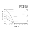
- FIG. 3 is a diagram showing the relationship between the line width of the channel and the measurement sensitivity.
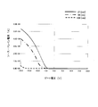
- FIG. 4 is a diagram showing the relationship between the thickness of the silicon oxide film 12b and the measurement sensitivity, and shows the relationship between the thickness of the silicon oxide film 12b and the source-drain current with respect to the gate voltage. As shown in FIG. 4, it can be seen that the thinner the silicon oxide film 12b, the larger the amount of change in the source-drain current with respect to the change in gate voltage; that is, the thinner the silicon oxide film 12b, the higher the measurement sensitivity. 4 that the thickness of the silicon oxide film 12b is preferably about 27 [nm] to 100 [nm] in terms of measurement sensitivity.
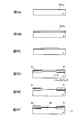
- FIG. 5 is a diagram illustrating a semiconductor manufacturing process of the sensor 10.
- a silicon oxide film (SiO 2 ) is formed on a silicon substrate by a thermal oxidation method.
- a polysilicon film is formed at a predetermined position (position of the channel 16) on the silicon oxide film.
- amorphous silicon is first deposited on the silicon oxide film, and polysilicon is formed by irradiating the amorphous silicon with a laser beam.
- an NPN channel 16 is formed by burying an impurity in the polysilicon film and diffusing the impurity by heat treatment.
- FIG. 5C shows, as an example, the case where the channel 16 is formed by making the polysilicon film an NPN type, but the channel 16 may be formed by making the polysilicon film a PNP type. Further, the channel 16 may be formed by making the polysilicon film NiP type or PiP type.
- the channel 16 is an NPN type or a PNP type
- the band gap is large, so that the leakage current is smaller than that of the NiP type or PiP type. For this reason, it is effective when configuring a circuit that is required to reduce current consumption in a standby state.
- the number of manufacturing steps of the NiN type and PiP type is one to two less than that of the NPN type and PNP type. For this reason, it is possible to reduce the cost, and it is effective when configuring a circuit in which the demand for reducing the consumption current in the standby state is not strict. In this way, a channel 16 made of polysilicon is formed.
- an interlayer insulating film 18 covering the channel 16 is formed.
- the interlayer insulating film 18 is omitted.
- the drain electrode 14 and the source electrode 15 are formed. Note that the drain electrode 14 and the source electrode 15 are electrically connected to the channel 16 through a contact hole.
- the silicon oxide film 12b, the drain electrode 14, the source electrode 15 and the channel 16 can be easily formed using the same semiconductor manufacturing process as that for manufacturing the TFT. Further, since the gate electrode 13 and the reaction field 20 are formed at positions different from the channel 16, the manufacture of the gate electrode 13 and the reaction field 20 is facilitated, and the area of the reaction field 20 and the like can be freely selected.
- silicon oxide films 12a and 12b which are insulating films, are formed on both surfaces of a silicon substrate 11.
- a gate electrode 13 is formed on the surface on which the silicon oxide film 12a is formed.
- a reference voltage Vref is applied to the gate electrode 13.
- the gate electrode 13, the silicon oxide film 12a, and the silicon substrate 11 have a metal-insulator-semiconductor (MIS) structure. Therefore, the gate voltage is not directly applied to the silicon substrate 11.
- the material of the gate electrode 13 is not particularly limited as long as it has conductivity. For example, a metal such as gold, platinum, titanium, and aluminum, or a conductive plastic may be used.
- drain electrode 14 and the source electrode 15 are formed on the surface on which the silicon oxide film 12b is formed.
- the drain electrode 14 and the source electrode 15 are electrically connected through the channel 16 on the silicon oxide film 12b.
- the sensor 10 includes the source electrode 15, the drain electrode 14 and the gate electrode 13 disposed on the silicon oxide films 12a and 12b, and the silicon oxide films 12a and 12b.
- a channel 16 disposed and electrically connected to the source electrode 15 and the drain electrode 14, and a reaction field 20 disposed on the silicon oxide films 12 a and 12 b, on the silicon oxide film 12 a different from the channel 16.
- a reaction field 20 is formed. With this configuration, the shape of the channel 16 and the area of the reaction field 20 can be independently selected. As a result, the sensor 10 with high measurement sensitivity and high degree of freedom in layout can be realized.
- the channel 16 is formed of polysilicon
- the silicon oxide film 12b, the drain electrode 14, the source electrode 15 and the channel 16 can be easily formed by using the same semiconductor manufacturing process as that for manufacturing the TFT. it can.
- the line width W of the channel 16 can be selected easily and with high accuracy in the semiconductor manufacturing process, so that measurement sensitivity can be selected easily and with high accuracy. can do.
- the interlayer insulating film 18 is formed and the drain electrode 14 and the source electrode 15 are electrically connected to the channel 16 through the contact holes is described.
- the film 18 may be omitted.
- a resist coating the P-type region of the channel 16 may be formed, and the drain electrode 14 and the source electrode 15 electrically separated by the resist may be directly formed on the silicon oxide film 12b.
- FIG. 6 is a cross-sectional view schematically showing the configuration of the sensor according to Embodiment 2 of the present invention.
- the same components as those in FIG. 2 are denoted by the same reference numerals, and description of overlapping portions is omitted.
- the gate electrode 13 and the reaction field 20 are formed on the silicon oxide film 12a on the back surface side with respect to the silicon oxide film 12b on which the drain electrode 14, the source electrode 15, and the channel 16 are formed has been described. .
- the gate electrode 13 and the reaction field 20 are formed on the silicon oxide film 12b.
- the sensor 30 forms the gate electrode 13 and the reaction field 20 on the same silicon oxide film 12b as the silicon oxide film 12b on which the drain electrode 14, the source electrode 15 and the channel 16 are formed.
- the silicon oxide film 12a of the sensor 30 shown in FIG. 6 may be omitted.
- the drain electrode 14, the source electrode 15, and the channel 16, which are sensing units, may be damaged by scattering of the detection target (sample solution) in the configuration shown in FIG. 2 rather than the configuration shown in FIG. May be lowered.
- the channel 16 is formed of polysilicon.
- the channel 16 may be formed of amorphous silicon. Even in this case, the silicon oxide film 12b, the drain electrode 14, the source electrode 15 and the channel 16 can be easily formed by using the same semiconductor manufacturing process as that for manufacturing the TFT.
- the sensor arranged on the silicon oxide film whose reaction field is different from that of the channel has been described.
- the reaction field is arranged on a silicon oxide film different from the channel, the restrictions on the shape of the channel, the area and position of the reaction field are reduced, and the measurement sensitivity and layout are reduced. The degree of freedom can be increased.
- the area over which the sample solution containing the substance to be detected spreads on the reaction field is constant. That is, if this area can be made constant, the region where the biomolecule reacts becomes constant, so the potential applied to the FET substrate becomes constant. As a result, the calibration curve with respect to the concentration is stabilized, and the accuracy of biosensing can be improved. Further, if biosensors having various reaction field areas can be manufactured, the user can select a biosensor having a reaction field area suitable for the experiment.
- Embodiments 3 to 5 a method for manufacturing a sensor capable of making the area where the sample solution spreads on the reaction field constant will be described. Also, a sensor manufacturing method that can be formed by freely selecting the area of the reaction field relatively easily will be described.
- FIG. 7 is a perspective view schematically showing the configuration of the sensor according to Embodiment 3 of the present invention.
- FIG. 8 is a cross-sectional view schematically showing the configuration of the sensor.
- the same components as those in FIG. 2 are denoted by the same reference numerals, and description of overlapping portions is omitted.
- silicon oxide films 12a and 12b which are insulating films, are formed on both surfaces of the silicon substrate 11. As shown in FIG.
- a gate electrode 43 is formed at a position facing the surface on which the silicon oxide film 12a is formed.
- a reference voltage Vref is applied to the gate electrode 43.
- the gate electrode 43, the silicon oxide film 12a, and the silicon substrate 11 form a metal-insulator-semiconductor (MIS) structure. Therefore, the gate voltage is not directly applied to the silicon substrate 11.
- the material of the gate electrode 43 is not particularly limited as long as it has conductivity, and may be a metal such as gold, platinum, titanium, aluminum, or conductive plastic.
- a drain 14 and a source 15 are formed on the surface on which the silicon oxide film 12b is formed.
- the drain 14 and the source 15 are electrically connected through the channel 16 on the silicon oxide film 12b.
- the channel 16 is made of, for example, polysilicon or carbon nanotube.
- a power source Vds and an ammeter 17 are connected between the drain 14 and the source 15 via an external wiring. Thereby, a predetermined voltage is applied between the drain 14 and the source 15 by the power source Vds, and the current flowing through the silicon substrate 11 is measured by the ammeter 17.
- the distance between the drain 14 and the source 15 is not particularly limited, but is usually about 0.5 to 10 ⁇ m. This spacing may be further reduced to facilitate connection between the electrodes by the channel 16.
- the shape and size of the source electrode and the drain electrode are not particularly limited, and may be set as appropriate according to the purpose.
- reaction field (gate oxide film) 50 facing the gate electrode 43 and a barrier 51 surrounding the reaction field 50 are formed on the surface on which the silicon oxide film 12a is formed. ing.
- the reaction field 50 has a function of immobilizing the target substance recognition molecule 60.
- both the reaction field 50 and the barrier portion 51 are formed of silicon oxide.
- target substance recognition molecule examples include antibodies, enzymes, proteins such as lectins, nucleic acids, oligosaccharides or polysaccharides, or substances having a structure thereof.
- the sensor of the present invention is used as a pH sensor or the like, it is not necessary to immobilize the substance to be detected.
- the thickness of the reaction field 50 is set to 200 [nm] or less, and is actually preferably about 1 to 200 nm (for example, 100 nm).
- the thickness of the barrier portion 51 is greater than the thickness of the reaction field 50 and is several thousand [nm] or less, and is actually preferably about 200 to 1000 nm (for example, 600 nm).
- the difference (that is, the step) between the upper surface of the reaction field 50 and the upper surface of the barrier portion 51 is preferably about 200 to 800 nm (for example, 500 nm).
- the area of the reaction field 50 is about 25 mm 2 .
- the barrier part 51 surrounds the reaction field 50 completely, it does not need to surround the reaction field 50 completely. In short, it is only necessary to surround the reaction solution 50 so that the outflow of the sample solution can be regulated.
- the senor 40 forms the barrier member 51 that surrounds the reaction field 50, so that when the detection target substance or the target substance recognition molecule is placed on the reaction field 50, these substances are detected. Can be prevented from being restricted by the barrier portion 51 and expanding beyond the area of the reaction field 50. That is, the area where the sample solution spreads on the reaction field 50 can be made constant.
- FIG. 9 is a diagram illustrating a semiconductor manufacturing process of the sensor 40.
- the biosensor manufacturing method according to the present embodiment is particularly characterized in that the barrier portion 51 is formed by using a LOCOS (Local Oxidation of Silicon) method. To do.
- LOCOS Local Oxidation of Silicon
- a silicon oxide film (SiO 2) is formed on a p-type silicon substrate by a thermal oxidation method.
- a silicon nitride film (Si 3 N 4 ) is deposited on the silicon oxide film by a CVD (Chemical Vapor Deposition) technique.
- the Si 3 N 4 film is removed by lithographic and etching techniques.
- the removed portion is a portion where the barrier portion 51 is formed.
- the portion where the Si 3 N 4 film remains is a portion where the reaction field 50 is formed.
- an oxidation treatment is performed in a wet O 2 atmosphere at a temperature of about 1000 ° C. Since Si 3 N 4 is not oxidized, only the portion from which Si 3 N 4 is removed is selectively oxidized. At this time, a part of the thick oxide film sinks directly under the Si 3 N 4 film (so-called bird's beak). In this way, the barrier portion 51 is formed.
- a gate oxide film that is, a reaction field 50 is formed by a thermal oxidation method or a vapor phase growth method.
- the silicon substrate is inverted, the source and drain are formed on the surface opposite to the surface on which the barrier portion 51 and the reaction field 50 are formed, the channel is formed, the interlayer film covering the channel is formed, and the external After performing the wiring process, a surface protective film is formed. Finally, the detection target substance recognition molecule 60 is fixed to the reaction field 50.
- the LOCOS method that has been conventionally used as an element isolation technique is used to form the barrier portion 51 that surrounds the reaction field.
- 51 and the reaction field 50 can be formed easily and with high accuracy.
- element isolation in the drain and the source is also formed by using the LOCOS method, the process of forming the drain 14 and the source 15 and the process of manufacturing the barrier portion 51 and the reaction field 50 can be partially shared. Processes and manufacturing equipment can be simplified.
- the element isolation between the drain and the source is not necessarily formed by using the LOCOS method. In short, it may be formed on a semiconductor substrate other than the region where the reaction field 50 and the barrier portion 51 are formed.
- FIG. 10 is a cross-sectional view schematically showing the configuration of the sensor according to Embodiment 4 of the present invention.
- the same components as those in FIG. 8 are denoted by the same reference numerals, and description of overlapping portions is omitted.
- the sensor 70 is attached with the gate electrode 43 fixed to the surface of the barrier portion 51. That is, the sensor 70 is fixedly attached to the surface of the barrier portion 51 without forming the gate electrode 43 at a position facing the reaction field 50.
- the gate electrode 43 is also formed in a square frame shape so as to be brought into contact with the entire upper surface of the barrier portion 51.
- the electric field passing through the reaction field 50 can be strengthened.
- the third and fourth embodiments have described the configuration of the sensor 40 called a so-called back gate type. That is, the case where the drain 14 and the source 15 are formed on the back surface side with respect to the silicon substrate surface on which the reaction field 50 and the barrier portion 51 are formed has been described.
- Embodiment 5 describes an application example of a side gate type biosensor.
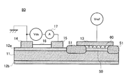
- FIG. 11 is a cross-sectional view schematically showing the configuration of the sensor according to Embodiment 5 of the present invention. The same components as those in FIG. 10 are denoted by the same reference numerals, and description of overlapping portions is omitted.
- the sensor 80 forms the drain 14 and the source 15 on the same surface side as the silicon substrate surface on which the reaction field 50 and the barrier portion 51 are formed. That is, the sensor 80 forms the drain 14 and the source 15 on the same surface side as the silicon substrate surface on which the reaction field 50 and the barrier portion 51 are formed.
- the same effect as in the case of the back gate type sensor of the third and fourth embodiments that is, the formation of the barrier portion 51 surrounding the reaction field 50, the reaction field 50
- the barrier portion 51 surrounding the reaction field 50
- the reaction field 50 When a substance to be detected or a substance to be detected is placed, it is possible to prevent these substances from being restricted by the barrier portion 51 and expanding beyond the area of the reaction field 50, and the area where the sample solution expands on the reaction field 50 Can be made constant.
- FIG. 12 is a diagram illustrating a semiconductor manufacturing process of the sensor according to the sixth embodiment of the present invention.
- a silicon oxide film is formed on a silicon substrate by a thermal oxidation method.
- the thickness of the silicon oxide film is set to a value obtained by subtracting the thickness of the reaction field 50 from the thickness of the barrier portion 51.
- a resist is applied to the entire surface of the silicon oxide, and an area corresponding to the reaction field 50 is exposed.
- the exposed resist is removed by development processing.
- a silicon oxide film having a thickness of the reaction field 50 is formed by a thermal oxidation method or a vapor phase growth method. Thereby, the reaction field 50 and the barrier part 51 thicker than the reaction field 50 can be formed.
- the names “sensor” and “sensor manufacturing method” are used. However, this is for convenience of explanation, and it is a matter of course that a biosensor or the like may be used. Furthermore, the types and number of detection target substances and detection target substance recognition molecules used by the sensor and the sensor manufacturing method are not limited to the above-described embodiments.
- the sensor and the sensor manufacturing method according to the present invention can be widely applied to a method for manufacturing a sensor including an FET.
Landscapes
- Health & Medical Sciences (AREA)
- Life Sciences & Earth Sciences (AREA)
- Chemical & Material Sciences (AREA)
- Molecular Biology (AREA)
- Physics & Mathematics (AREA)
- Chemical Kinetics & Catalysis (AREA)
- Microelectronics & Electronic Packaging (AREA)
- Engineering & Computer Science (AREA)
- Spectroscopy & Molecular Physics (AREA)
- Electrochemistry (AREA)
- Analytical Chemistry (AREA)
- Biochemistry (AREA)
- General Health & Medical Sciences (AREA)
- General Physics & Mathematics (AREA)
- Immunology (AREA)
- Pathology (AREA)
- Thin Film Transistor (AREA)
- Investigating Or Analyzing Materials By The Use Of Electric Means (AREA)
Abstract
Provided is a sensor having a high sensitivity and a high degree of freedom of layout by reducing constrictions of the channel shape, the reaction field area, and the position. Provided is also a method for manufacturing the sensor. The sensor (10) includes: a source electrode (15), a drain electrode, (14), and a gate electrode (13) arranged on silicon oxide film (12a, 12b); a channel (16) arranged on the silicon oxide films (12a, 12b) and electrically connected to the source electrode (15) and the drain electrode (14); and a reaction field (20) arranged on the silicon oxide films (12a, 12b). The reaction field (20) is formed on the silicon oxide film (12a) which is different from the channel (16). With this configuration, it is possible to independently select the shape of the channel (16) and the area of the reaction field (20). This enables the sensor (10) to have a high measurement sensitivity and a high degree of freedom of layout.
Description
本発明は、例えばバイオセンサやpHセンサ等として使用されるセンサ及びその製造方法に関し、特にFET(Field Effect Transistor:電界効果トランジスタ)を備えたセンサ及びその製造方法に関する。
The present invention relates to a sensor used as, for example, a biosensor or a pH sensor and a manufacturing method thereof, and more particularly to a sensor including a FET (Field Effect Transistor) and a manufacturing method thereof.
従来、バイオセンサやpHセンサ等のセンサにおいて、FETを用いたものが提案されている(特許文献1~3参照)。一般に、FETを利用したセンサでは、ソース電極及びドレイン電極が、絶縁膜上に形成されたチャネルによって電気的に接続されている。チャネル上には、被検出物質の反応場が形成されている。反応場には、被検出物質を固定化するための反応膜が設けられている。そして、通常、反応膜の上から、ゲート電極によってゲート電圧を印加し、そのときのソース-ドレイン電流を測定することにより、反応場に提供されている被検出物質の濃度等を測定する。
Conventionally, sensors such as biosensors and pH sensors using FETs have been proposed (see Patent Documents 1 to 3). In general, in a sensor using an FET, a source electrode and a drain electrode are electrically connected by a channel formed on an insulating film. A reaction field for the substance to be detected is formed on the channel. The reaction field is provided with a reaction membrane for immobilizing the substance to be detected. Then, usually, the gate voltage is applied from above the reaction film by the gate electrode, and the source-drain current at that time is measured to measure the concentration of the substance to be detected provided in the reaction field.
ところで、上述したようなセンサにおいては、チャネルが感知部として機能する。従って、チャネルの形状に応じて、ゲート電圧に対するソース-ドレイン電流の変化量(つまり測定感度)が異なる。よって、チャネルの形状は、測定しようとする被検出物の種類等に応じて、自由に選択できることが望ましい。
By the way, in the sensor as described above, the channel functions as a sensing unit. Therefore, the amount of change in source-drain current with respect to the gate voltage (that is, measurement sensitivity) varies depending on the shape of the channel. Therefore, it is desirable that the shape of the channel can be freely selected according to the type of the detection object to be measured.
一方で、反応場の面積も、被検出物質からFET基板にかかるポテンシャルに影響を及ぼす。従って、反応場の面積によっても測定感度が異なる。よって、反応場の面積も、測定しようとする被検出物の種類等に応じて、自由に選択できることが望ましい。さらに、反応場の位置は、ユーザの使い勝手や、センサとしてのレイアウト等を考えると、選択の幅が広い方が望ましい。
On the other hand, the area of the reaction field also affects the potential applied to the FET substrate from the substance to be detected. Therefore, the measurement sensitivity varies depending on the area of the reaction field. Therefore, it is desirable that the area of the reaction field can also be freely selected according to the type of the object to be detected. Further, the position of the reaction field is preferably wider when considering user convenience, layout as a sensor, and the like.
本発明は、チャネルの形状、反応場の面積及び位置の制約を少なくして、測定感度及びレイアウトの自由度の高いセンサ及びその製造方法を提供する。
The present invention provides a sensor having a high measurement sensitivity and a high degree of freedom in layout, and a manufacturing method thereof, by reducing restrictions on the shape of the channel, the area and position of the reaction field.
本発明の第一は、酸化シリコン膜を有するシリコン基板と、前記酸化シリコン膜に配置されたソース電極、ドレイン電極及びゲート電極と、ポリシリコン又はアモルファスシリコンからなり、前記酸化シリコン膜に配置され、前記ソース電極及びドレイン電極に電気的に接続されたチャネルと、前記酸化シリコン膜上に配置された反応場と、を備えるセンサに関する。
The first of the present invention comprises a silicon substrate having a silicon oxide film, a source electrode, a drain electrode and a gate electrode disposed on the silicon oxide film, and polysilicon or amorphous silicon, and is disposed on the silicon oxide film, The present invention relates to a sensor including a channel electrically connected to the source electrode and the drain electrode, and a reaction field disposed on the silicon oxide film.
本発明の第二は、半導体基板と、前記半導体基板の表面に形成された酸化シリコン膜と、前記酸化シリコン膜に接続された電極とを有し、前記酸化シリコン膜の一部が被検出物の反応場として使用される、FETを含むセンサの製造方法であって:シリコン基板に酸化シリコン膜を形成する工程と、前記酸化シリコン膜に、ポリシリコン膜又はアモルファスシリコン膜を形成する工程と、前記ポリシリコン膜又はアモルファスシリコン膜に不純物をドーピングする工程と、前記不純物がドーピングされた前記ポリシリコン膜又はアモルファスシリコン膜にソース電極及びドレイン電極を形成する工程と、前記酸化シリコン膜にゲート電極を形成する工程と、前記酸化シリコン膜に反応場を形成する工程と、を含む製造方法に関する。
A second aspect of the present invention includes a semiconductor substrate, a silicon oxide film formed on the surface of the semiconductor substrate, and an electrode connected to the silicon oxide film, and a part of the silicon oxide film is an object to be detected. A method of manufacturing a sensor including an FET used as a reaction field of: a step of forming a silicon oxide film on a silicon substrate; a step of forming a polysilicon film or an amorphous silicon film on the silicon oxide film; Doping the polysilicon film or amorphous silicon film with an impurity; forming a source electrode and a drain electrode on the polysilicon film or amorphous silicon film doped with the impurity; and forming a gate electrode on the silicon oxide film. The present invention relates to a manufacturing method including a step of forming and a step of forming a reaction field in the silicon oxide film.
本発明によれば、反応場がチャネルとは異なる酸化シリコン膜上に配置されるので、チャネルの形状、反応場の面積及び位置の制約が少なくなり、測定感度及びレイアウトの自由度を高くすることができる。また、チャネルがポリシリコン又はアモルファスシリコンで形成されるので、TFTを製造するのと同様の半導体製造工程を用いて、容易に酸化シリコン膜、ドレイン電極、ソース電極及びチャネルを形成することができ、チャネルの幅及び酸化シリコン膜の厚さも容易に選択できる。この結果、測定感度を容易に変更できるようになる。
According to the present invention, since the reaction field is arranged on a silicon oxide film different from the channel, restrictions on the shape of the channel, the area and position of the reaction field are reduced, and the measurement sensitivity and the freedom of layout are increased. Can do. In addition, since the channel is formed of polysilicon or amorphous silicon, a silicon oxide film, a drain electrode, a source electrode, and a channel can be easily formed using a semiconductor manufacturing process similar to that for manufacturing a TFT. The channel width and silicon oxide film thickness can also be easily selected. As a result, the measurement sensitivity can be easily changed.
以下、本発明の実施の形態について、図面を参照して詳細に説明する。
Hereinafter, embodiments of the present invention will be described in detail with reference to the drawings.
(実施の形態1)
〔センサの構成〕
図1は、本発明の実施の形態1に係るセンサの構成を模式的に示す斜視図である。図2は、上記センサの構成を模式的に示す断面図である。本実施の形態は、本発明のセンサをバイオセンサやpHセンサ等に適用した例である。 (Embodiment 1)
[Sensor configuration]
FIG. 1 is a perspective view schematically showing a configuration of a sensor according to Embodiment 1 of the present invention. FIG. 2 is a cross-sectional view schematically showing the configuration of the sensor. This embodiment is an example in which the sensor of the present invention is applied to a biosensor, a pH sensor, or the like.
図1及び図2に示すように、センサ10は、シリコン基板11の両面に、絶縁膜である酸化シリコン膜12a,12bが形成されている。
As shown in FIGS. 1 and 2, in the sensor 10, silicon oxide films 12a and 12b, which are insulating films, are formed on both surfaces of a silicon substrate 11.
酸化シリコン膜12aが形成された面には、ゲート電極13が形成されている。ゲート電極13には、参照電圧Vrefが印加される。ゲート電極13、酸化シリコン膜12a及びシリコン基板11は、金属-絶縁体-半導体(Metal-Insulator-Semiconductor:MIS)構造となっている。したがって、ゲート電圧はシリコン基板11に直接印加されない。ゲート電極13の材質は、導電性を有するものであれば特に限定されず、例えば金、白金、チタン、アルミニウムなどの金属や導電性プラスチックなどであればよい。
A gate electrode 13 is formed on the surface on which the silicon oxide film 12a is formed. A reference voltage Vref is applied to the gate electrode 13. The gate electrode 13, the silicon oxide film 12a, and the silicon substrate 11 have a metal-insulator-semiconductor (MIS) structure. Therefore, the gate voltage is not directly applied to the silicon substrate 11. The material of the gate electrode 13 is not particularly limited as long as it has conductivity. For example, a metal such as gold, platinum, titanium, and aluminum, or a conductive plastic may be used.
一方、酸化シリコン膜12bが形成された面には、ドレイン電極14及びソース電極15が形成されている。ドレイン電極14とソース電極15は、酸化シリコン膜12b上で、チャネル16を介して電気的に接続されている。
On the other hand, the drain electrode 14 and the source electrode 15 are formed on the surface on which the silicon oxide film 12b is formed. The drain electrode 14 and the source electrode 15 are electrically connected through the channel 16 on the silicon oxide film 12b.
本実施の形態の場合、チャネル16は、ポリシリコンで形成されている。これにより、酸化シリコン膜12b、ドレイン電極14、ソース電極15及びチャネル16は、一般的なTFT(Thin Film Transistor)構造とされているので、TFTを製造するのと同様の半導体製造工程を用いて、容易に酸化シリコン膜12b、ドレイン電極14、ソース電極15及びチャネル16を形成することができる。
In the case of this embodiment, the channel 16 is made of polysilicon. As a result, the silicon oxide film 12b, the drain electrode 14, the source electrode 15 and the channel 16 have a general TFT (Thin-Film-Transistor) structure. Therefore, the same semiconductor manufacturing process as that used to manufacture the TFT is used. The silicon oxide film 12b, the drain electrode 14, the source electrode 15 and the channel 16 can be easily formed.
また、チャネル16はポリシリコンで形成されているので、チャネル16をカーボンナノチューブ等によって形成する場合と比較して、チャネル16の線路幅Wを、半導体製造工程のなかで、容易に選択できるようになる。
Further, since the channel 16 is formed of polysilicon, the line width W of the channel 16 can be easily selected in the semiconductor manufacturing process as compared with the case where the channel 16 is formed of carbon nanotubes or the like. Become.
ドレイン電極14とソース電極15の間には、外部配線を介して電源Vds及び電流計17が接続されている。これにより、電源Vdsによってドレイン電極14とソース電極15との間に所定の電圧が印加され、電流計17によってシリコン基板11に流れる電流が測定される。
A power source Vds and an ammeter 17 are connected between the drain electrode 14 and the source electrode 15 via an external wiring. Thereby, a predetermined voltage is applied between the drain electrode 14 and the source electrode 15 by the power source Vds, and the current flowing through the silicon substrate 11 is measured by the ammeter 17.
ドレイン電極14とソース電極15との間隔は、特に限定されないが、通常は0.5~10[μm]程度である。この間隔は、チャネル16による電極間の接続を容易にするためにさらに縮めてもよい。ソース電極及びドレイン電極の形状及び大きさは特に限定されず、目的に応じて適宜設定すればよい。
The distance between the drain electrode 14 and the source electrode 15 is not particularly limited, but is usually about 0.5 to 10 [μm]. This spacing may be further reduced to facilitate connection between the electrodes by the channel 16. The shape and size of the source electrode and the drain electrode are not particularly limited, and may be set as appropriate according to the purpose.
ここで、図2に示すように、酸化シリコン膜12aが形成された面には、反応場20が形成されている。反応場20とは、試料溶液を提供する領域を意味する。
Here, as shown in FIG. 2, a reaction field 20 is formed on the surface on which the silicon oxide film 12a is formed. The reaction field 20 means a region that provides a sample solution.
反応場20とゲート電極13は、酸化シリコン膜12a,12bのうち、同一の面の酸化シリコン膜(図2の場合、酸化シリコン膜12a)に配置されることが好ましい。また、反応場20とゲート電極13は、同一の酸化シリコン膜12a上のできるだけ近い位置に形成されることが好ましい。例えば、反応場20の上側にゲート電極13を配置してもよく、反応場20の周囲にゲート電極13を形成してもよい。このようにすることで、反応場20に提供された被検出物の濃度変化等に対するチャネル16での電圧変化を大きくできるので、測定感度を高めることができる。
The reaction field 20 and the gate electrode 13 are preferably arranged on the same surface of the silicon oxide films 12a and 12b (in the case of FIG. 2, the silicon oxide film 12a). The reaction field 20 and the gate electrode 13 are preferably formed as close as possible on the same silicon oxide film 12a. For example, the gate electrode 13 may be disposed above the reaction field 20, and the gate electrode 13 may be formed around the reaction field 20. By doing in this way, since the voltage change in the channel 16 with respect to the change in the concentration of the object to be detected provided to the reaction field 20 can be increased, the measurement sensitivity can be increased.
反応場20が配置された領域の酸化シリコン膜12aの厚さは、その周囲の酸化シリコン膜12aの厚さよりも薄いことが好ましい。すなわち、反応場20は凹部の内部にあることが好ましい。これにより、試料溶液を反応場20に効率的に留めることができるだけでなく、ゲート電極13から基板面方向に漏れ出た電気力線をより効率的に反応場20を通過させることができる。また、酸化シリコン膜12a上に、反応場20を取り囲む障壁を設けても、試料溶液を反応場20に効率的に留めることができる。
It is preferable that the thickness of the silicon oxide film 12a in the region where the reaction field 20 is disposed is thinner than the thickness of the surrounding silicon oxide film 12a. That is, the reaction field 20 is preferably inside the recess. Thereby, not only the sample solution can be efficiently retained in the reaction field 20, but also the electric lines of force leaking from the gate electrode 13 toward the substrate surface can be passed through the reaction field 20 more efficiently. Even if a barrier surrounding the reaction field 20 is provided on the silicon oxide film 12a, the sample solution can be efficiently retained in the reaction field 20.
センサ10をバイオセンサとして使用する場合、反応場20に、抗体や酵素、レクチンなどのタンパク質、核酸、オリゴ糖又は多糖、あるいはそれらの構造を有する物質である被検出物質認識分子21を固定化するとよい。被検出物質認識分子を反応領域に固定化することで、特定のタンパク質や化学物質などを特異的に検出することができる。なお、センサ10をpHセンサ等として使用する場合には、反応場20に、被検出物質認識分子21を固定する必要はない。
When the sensor 10 is used as a biosensor, a detection substance recognition molecule 21 that is a substance having an antibody, an enzyme, a protein such as a lectin, a nucleic acid, an oligosaccharide or a polysaccharide, or a structure thereof is immobilized on the reaction field 20. Good. By immobilizing the target substance recognition molecule in the reaction region, a specific protein, chemical substance, or the like can be specifically detected. When the sensor 10 is used as a pH sensor or the like, it is not necessary to immobilize the substance to be detected recognition molecule 21 in the reaction field 20.
図3は、チャネルの線路幅と測定感度との関係を示す図であり、チャネル16をポリシリコンで形成した場合における、チャネル16の線路幅Wと、ゲート電圧に対するソース-ドレイン電流との関係を示す。図3に示されるように、チャネル16の線路幅Wが広くなるほど、ゲート電圧の変化に対するソース-ドレイン電流の変化量が大きいこと;すなわち線路幅Wを広くするほど測定感度を高くできることが分かる。また、図3から、測定感度の点で、チャネル16の線路幅Wは、50[μm]~200[μm]程度であることが好ましいことが分かる。
FIG. 3 is a diagram showing the relationship between the line width of the channel and the measurement sensitivity. The relationship between the line width W of the channel 16 and the source-drain current with respect to the gate voltage when the channel 16 is formed of polysilicon. Show. As shown in FIG. 3, it can be seen that as the line width W of the channel 16 increases, the amount of change in the source-drain current with respect to the change in the gate voltage increases; that is, as the line width W increases, the measurement sensitivity can be increased. 3 that the line width W of the channel 16 is preferably about 50 [μm] to 200 [μm] in terms of measurement sensitivity.
さらに、半導体製造工程のなかで、酸化シリコン膜12bの厚さ選択することで、測定感度を調整することもできる。図4は、酸化シリコン膜12bの厚さと測定感度との関係を示す図であり、酸化シリコン膜12bの厚さと、ゲート電圧に対するソース-ドレイン電流との関係を示す。図4に示されるように、酸化シリコン膜12bが薄くなるほど、ゲート電圧の変化に対するソース-ドレイン電流の変化量が大きいこと;すなわち酸化シリコン膜12bを薄くするほど測定感度を高くできることが分かる。また、図4から、測定感度の点で、酸化シリコン膜12bの厚さは、27[nm]~100[nm]程度であることが好ましいことが分かる。
Furthermore, the measurement sensitivity can be adjusted by selecting the thickness of the silicon oxide film 12b in the semiconductor manufacturing process. FIG. 4 is a diagram showing the relationship between the thickness of the silicon oxide film 12b and the measurement sensitivity, and shows the relationship between the thickness of the silicon oxide film 12b and the source-drain current with respect to the gate voltage. As shown in FIG. 4, it can be seen that the thinner the silicon oxide film 12b, the larger the amount of change in the source-drain current with respect to the change in gate voltage; that is, the thinner the silicon oxide film 12b, the higher the measurement sensitivity. 4 that the thickness of the silicon oxide film 12b is preferably about 27 [nm] to 100 [nm] in terms of measurement sensitivity.
〔センサの製造方法〕
以下、上述のように構成されたセンサ10の製造方法について説明する。図5は、センサ10の半導体製造工程を示す図である。 [Sensor manufacturing method]
Hereinafter, a method for manufacturing thesensor 10 configured as described above will be described. FIG. 5 is a diagram illustrating a semiconductor manufacturing process of the sensor 10.
以下、上述のように構成されたセンサ10の製造方法について説明する。図5は、センサ10の半導体製造工程を示す図である。 [Sensor manufacturing method]
Hereinafter, a method for manufacturing the
まず、図5Aに示すように、シリコン基板上に、熱酸化法によって酸化シリコン膜(SiO2)を形成する。
First, as shown in FIG. 5A, a silicon oxide film (SiO 2 ) is formed on a silicon substrate by a thermal oxidation method.
次に、図5Bに示すように、酸化シリコン膜上の所定位置(チャネル16の位置)にポリシリコン膜を形成する。この場合、例えば、先ず酸化シリコン膜にアモルファスシリコンを堆積させ、このアモルファスシリコンにレーザービームを照射することによりポリシリコンを形成すればよい。
Next, as shown in FIG. 5B, a polysilicon film is formed at a predetermined position (position of the channel 16) on the silicon oxide film. In this case, for example, amorphous silicon is first deposited on the silicon oxide film, and polysilicon is formed by irradiating the amorphous silicon with a laser beam.
次に、図5Cに示すように、ポリシリコン膜に不純物を埋め込み、熱処理によりこの不純物を拡散することにより、NPN型のチャネル16を形成する。図5Cには、一例として、ポリシリコン膜をNPN型にすることでチャネル16を形成した場合が示されているが、ポリシリコン膜をPNP型とすることでチャネル16を形成してもよい。また、ポリシリコン膜をNiP型又はPiP型とすることでチャネル16を形成してもよい。
Next, as shown in FIG. 5C, an NPN channel 16 is formed by burying an impurity in the polysilicon film and diffusing the impurity by heat treatment. FIG. 5C shows, as an example, the case where the channel 16 is formed by making the polysilicon film an NPN type, but the channel 16 may be formed by making the polysilicon film a PNP type. Further, the channel 16 may be formed by making the polysilicon film NiP type or PiP type.
チャネル16をNPN型又はPNP型とした場合には、バンドギャップが大きくなるので、NiP型やPiP型に比べリーク電流が小さい。このため、待機状態の消費電流を少なくすることが求められる回路を構成する場合に有効である。一方、NiN型やPiP型は、製造工程数がNPN型やPNP型と比べて1~2工程少ない。このため、原価を低減することが可能であり、待機状態の消費電流を少なくすることへの要求が厳しくない回路を構成する場合に有効である。このようにして、ポリシリコンでなるチャネル16が形成される。
When the channel 16 is an NPN type or a PNP type, the band gap is large, so that the leakage current is smaller than that of the NiP type or PiP type. For this reason, it is effective when configuring a circuit that is required to reduce current consumption in a standby state. On the other hand, the number of manufacturing steps of the NiN type and PiP type is one to two less than that of the NPN type and PNP type. For this reason, it is possible to reduce the cost, and it is effective when configuring a circuit in which the demand for reducing the consumption current in the standby state is not strict. In this way, a channel 16 made of polysilicon is formed.
次に、図5Dに示すように、チャネル16を被覆する層間絶縁膜18を形成する。なお、図2Dでは、図を簡単化するために、層間絶縁膜18は省略して示されている。
Next, as shown in FIG. 5D, an interlayer insulating film 18 covering the channel 16 is formed. In FIG. 2D, in order to simplify the drawing, the interlayer insulating film 18 is omitted.
次に、図5Eに示すように、ドレイン電極14及びソース電極15を形成する。なお、ドレイン電極14及びソース電極15は、コンタクトホールを通してチャネル16に電気的に接続される。
Next, as shown in FIG. 5E, the drain electrode 14 and the source electrode 15 are formed. Note that the drain electrode 14 and the source electrode 15 are electrically connected to the channel 16 through a contact hole.
次に、図2に示すように、ドレイン電極14とソース電極15とを電流計17を介して接続する処理(外部配線処理)を行う。次に、図2に示すように、酸化シリコン膜12a上にゲート電極13を形成した後、反応場20を形成する。
Next, as shown in FIG. 2, a process (external wiring process) for connecting the drain electrode 14 and the source electrode 15 via the ammeter 17 is performed. Next, as shown in FIG. 2, after forming the gate electrode 13 on the silicon oxide film 12a, the reaction field 20 is formed.
このように、TFTを製造するのと同様の半導体製造工程を用いて、酸化シリコン膜12b、ドレイン電極14、ソース電極15及びチャネル16を容易に形成することができる。また、ゲート電極13及び反応場20をチャネル16とは異なる位置に形成するので、ゲート電極13及び反応場20の製造も容易となり、かつ反応場20の面積等も自由に選択できるようになる。
Thus, the silicon oxide film 12b, the drain electrode 14, the source electrode 15 and the channel 16 can be easily formed using the same semiconductor manufacturing process as that for manufacturing the TFT. Further, since the gate electrode 13 and the reaction field 20 are formed at positions different from the channel 16, the manufacture of the gate electrode 13 and the reaction field 20 is facilitated, and the area of the reaction field 20 and the like can be freely selected.
図1及び図2に示すように、センサ10は、シリコン基板11の両面に、絶縁膜である酸化シリコン膜12a,12bが形成されている。
As shown in FIGS. 1 and 2, in the sensor 10, silicon oxide films 12a and 12b, which are insulating films, are formed on both surfaces of a silicon substrate 11.
酸化シリコン膜12aが形成された面には、ゲート電極13が形成されている。ゲート電極13には、参照電圧Vrefが印加される。ゲート電極13、酸化シリコン膜12a及びシリコン基板11は、金属-絶縁体-半導体(Metal-Insulator-Semiconductor:MIS)構造となっている。したがって、ゲート電圧はシリコン基板11に直接印加されない。ゲート電極13の材質は、導電性を有するものであれば特に限定されず、例えば金、白金、チタン、アルミニウムなどの金属や導電性プラスチックなどであればよい。
A gate electrode 13 is formed on the surface on which the silicon oxide film 12a is formed. A reference voltage Vref is applied to the gate electrode 13. The gate electrode 13, the silicon oxide film 12a, and the silicon substrate 11 have a metal-insulator-semiconductor (MIS) structure. Therefore, the gate voltage is not directly applied to the silicon substrate 11. The material of the gate electrode 13 is not particularly limited as long as it has conductivity. For example, a metal such as gold, platinum, titanium, and aluminum, or a conductive plastic may be used.
一方、酸化シリコン膜12bが形成された面には、ドレイン電極14及びソース電極15が形成されている。ドレイン電極14とソース電極15は、酸化シリコン膜12b上で、チャネル16を介して電気的に接続されている。
On the other hand, the drain electrode 14 and the source electrode 15 are formed on the surface on which the silicon oxide film 12b is formed. The drain electrode 14 and the source electrode 15 are electrically connected through the channel 16 on the silicon oxide film 12b.
以上詳細に説明したように、本実施の形態によれば、センサ10は、酸化シリコン膜12a,12bに配置されたソース電極15、ドレイン電極14及びゲート電極13と、酸化シリコン膜12a,12bに配置され、ソース電極15及びドレイン電極14に電気的に接続されたチャネル16と、酸化シリコン膜12a,12b上に配置された反応場20とを備え、チャネル16とは異なる酸化シリコン膜12a上に反応場20を形成する。この構成により、チャネル16の形状及び反応場20の面積をそれぞれ独立に選択できるようになる。その結果、測定感度及びレイアウトの自由度の高いセンサ10を実現することができる。
As described above in detail, according to the present embodiment, the sensor 10 includes the source electrode 15, the drain electrode 14 and the gate electrode 13 disposed on the silicon oxide films 12a and 12b, and the silicon oxide films 12a and 12b. A channel 16 disposed and electrically connected to the source electrode 15 and the drain electrode 14, and a reaction field 20 disposed on the silicon oxide films 12 a and 12 b, on the silicon oxide film 12 a different from the channel 16. A reaction field 20 is formed. With this configuration, the shape of the channel 16 and the area of the reaction field 20 can be independently selected. As a result, the sensor 10 with high measurement sensitivity and high degree of freedom in layout can be realized.
また、チャネル16をポリシリコンで形成したことにより、TFTを製造するのと同様の半導体製造工程を用いて、容易に酸化シリコン膜12b、ドレイン電極14、ソース電極15及びチャネル16を形成することができる。また、チャネル16をカーボンナノチューブ等によって形成する場合と比較して、チャネル16の線路幅Wを、半導体製造工程のなかで、容易かつ高精度で選択できるので、測定感度を容易かつ高精度で選択することができる。
Further, since the channel 16 is formed of polysilicon, the silicon oxide film 12b, the drain electrode 14, the source electrode 15 and the channel 16 can be easily formed by using the same semiconductor manufacturing process as that for manufacturing the TFT. it can. Compared to the case where the channel 16 is formed of carbon nanotubes or the like, the line width W of the channel 16 can be selected easily and with high accuracy in the semiconductor manufacturing process, so that measurement sensitivity can be selected easily and with high accuracy. can do.
なお、本実施の形態では、図5Eに示すように、層間絶縁膜18を形成し、コンタクトホールを通してドレイン電極14及びソース電極15をチャネル16に電気的に接続した場合について述べたが、層間絶縁膜18を省略してもよい。その場合、例えば、チャネル16のP型領域を被膜するレジストを形成し、このレジストによって電気的に分離されたドレイン電極14及びソース電極15を酸化シリコン膜12b上に直接形成すればよい。
In the present embodiment, as shown in FIG. 5E, the case where the interlayer insulating film 18 is formed and the drain electrode 14 and the source electrode 15 are electrically connected to the channel 16 through the contact holes is described. The film 18 may be omitted. In that case, for example, a resist coating the P-type region of the channel 16 may be formed, and the drain electrode 14 and the source electrode 15 electrically separated by the resist may be directly formed on the silicon oxide film 12b.
(実施の形態2)
図6は、本発明の実施の形態2に係るセンサの構成を模式的に示す断面図である。図2と同一構成部分には同一符号を付して重複箇所の説明を省略する。 (Embodiment 2)
FIG. 6 is a cross-sectional view schematically showing the configuration of the sensor according toEmbodiment 2 of the present invention. The same components as those in FIG. 2 are denoted by the same reference numerals, and description of overlapping portions is omitted.
図6は、本発明の実施の形態2に係るセンサの構成を模式的に示す断面図である。図2と同一構成部分には同一符号を付して重複箇所の説明を省略する。 (Embodiment 2)
FIG. 6 is a cross-sectional view schematically showing the configuration of the sensor according to
実施の形態1は、ドレイン電極14、ソース電極15及びチャネル16が形成された酸化シリコン膜12bに対して裏面側の酸化シリコン膜12a上にゲート電極13及び反応場20を形成した場合について説明した。実施の形態2では、酸化シリコン膜12b上にゲート電極13及び反応場20を形成する例について説明する。
In the first embodiment, the case where the gate electrode 13 and the reaction field 20 are formed on the silicon oxide film 12a on the back surface side with respect to the silicon oxide film 12b on which the drain electrode 14, the source electrode 15, and the channel 16 are formed has been described. . In the second embodiment, an example in which the gate electrode 13 and the reaction field 20 are formed on the silicon oxide film 12b will be described.
図6に示すように、センサ30は、ドレイン電極14、ソース電極15及びチャネル16が形成された酸化シリコン膜12bと同一の酸化シリコン膜12bにゲート電極13及び反応場20を形成する。図6に示すセンサ30の酸化シリコン膜12aは省略されてもよい。
As shown in FIG. 6, the sensor 30 forms the gate electrode 13 and the reaction field 20 on the same silicon oxide film 12b as the silicon oxide film 12b on which the drain electrode 14, the source electrode 15 and the channel 16 are formed. The silicon oxide film 12a of the sensor 30 shown in FIG. 6 may be omitted.
図6のように構成するよりも、図2のように構成する方が、センシング部であるドレイン電極14、ソース電極15及びチャネル16が被検出物(試料溶液)の飛散によって損傷を受ける可能性を低くできる場合がある。
The drain electrode 14, the source electrode 15, and the channel 16, which are sensing units, may be damaged by scattering of the detection target (sample solution) in the configuration shown in FIG. 2 rather than the configuration shown in FIG. May be lowered.
なお、実施の形態1及び2では、チャネル16をポリシリコンによって形成した場合について説明したが、チャネル16はアモルファスシリコンによって形成してもよい。この場合でも、TFTを製造するのと同様の半導体製造工程を用いて、容易に酸化シリコン膜12b、ドレイン電極14、ソース電極15及びチャネル16を形成することができる。
In the first and second embodiments, the case where the channel 16 is formed of polysilicon has been described. However, the channel 16 may be formed of amorphous silicon. Even in this case, the silicon oxide film 12b, the drain electrode 14, the source electrode 15 and the channel 16 can be easily formed by using the same semiconductor manufacturing process as that for manufacturing the TFT.
上記実施の形態1及び2では、反応場がチャネルとは異なる酸化シリコン膜上に配置されるセンサについて説明した。上記実施の形態1及び2に係るセンサは、反応場がチャネルとは異なる酸化シリコン膜上に配置されるので、チャネルの形状、反応場の面積及び位置の制約が少なくなり、測定感度及びレイアウトの自由度を高くすることができる。
In the first and second embodiments described above, the sensor arranged on the silicon oxide film whose reaction field is different from that of the channel has been described. In the sensors according to the first and second embodiments, since the reaction field is arranged on a silicon oxide film different from the channel, the restrictions on the shape of the channel, the area and position of the reaction field are reduced, and the measurement sensitivity and layout are reduced. The degree of freedom can be increased.
ところで、バイオセンサにおいて、検出精度を向上させるためには、被検出物質を含む試料溶液が反応場上で拡がる面積が一定であることが望ましい。つまり、この面積を一定にできれば、生体分子が反応する領域が一定になるので、FET基板にかかるポテンシャルが一定になる。この結果、濃度に対する検量線が安定化され、バイオセンシングの精度を向上させることができる。また、反応場の面積が様々なバイオセンサを製造できれば、ユーザは、その中から実験に適した反応場面積を有するバイオセンサを選択できるようになる。
By the way, in order to improve detection accuracy in a biosensor, it is desirable that the area over which the sample solution containing the substance to be detected spreads on the reaction field is constant. That is, if this area can be made constant, the region where the biomolecule reacts becomes constant, so the potential applied to the FET substrate becomes constant. As a result, the calibration curve with respect to the concentration is stabilized, and the accuracy of biosensing can be improved. Further, if biosensors having various reaction field areas can be manufactured, the user can select a biosensor having a reaction field area suitable for the experiment.
実施の形態3~5では、試料溶液が反応場上で拡がる面積を一定とすることができるセンサの製造方法について説明する。また、比較的容易に、反応場の面積を自由に選択して形成できるセンサ製造方法について説明する。
In Embodiments 3 to 5, a method for manufacturing a sensor capable of making the area where the sample solution spreads on the reaction field constant will be described. Also, a sensor manufacturing method that can be formed by freely selecting the area of the reaction field relatively easily will be described.
(実施の形態3)
〔センサの構成〕
図7は、本発明の実施の形態3に係るセンサの構成を模式的に示す斜視図である。図8は、上記センサの構成を模式的に示す断面図である。図2と同一構成部分には同一符号を付して重複箇所の説明を省略する。 (Embodiment 3)
[Sensor configuration]
FIG. 7 is a perspective view schematically showing the configuration of the sensor according to Embodiment 3 of the present invention. FIG. 8 is a cross-sectional view schematically showing the configuration of the sensor. The same components as those in FIG. 2 are denoted by the same reference numerals, and description of overlapping portions is omitted.
図7及び図8に示すように、センサ40は、シリコン基板11の両面に、絶縁膜である酸化シリコン膜12a、12bが形成されている。
7 and 8, in the sensor 40, silicon oxide films 12a and 12b, which are insulating films, are formed on both surfaces of the silicon substrate 11. As shown in FIG.
酸化シリコン膜12aが形成された面に対向する位置には、ゲート電極43が形成されている。ゲート電極43には、参照電圧Vrefが印加される。ゲート電極43、酸化シリコン膜12a及びシリコン基板11は、金属-絶縁体-半導体(MIS)構造を形成する。したがって、ゲート電圧はシリコン基板11に直接印加されない。ゲート電極43の材質は、導電性を有するものであれば特に限定されず、例えば金、白金、チタン、アルミニウムなどの金属や導電性プラスチックなどであればよい。
A gate electrode 43 is formed at a position facing the surface on which the silicon oxide film 12a is formed. A reference voltage Vref is applied to the gate electrode 43. The gate electrode 43, the silicon oxide film 12a, and the silicon substrate 11 form a metal-insulator-semiconductor (MIS) structure. Therefore, the gate voltage is not directly applied to the silicon substrate 11. The material of the gate electrode 43 is not particularly limited as long as it has conductivity, and may be a metal such as gold, platinum, titanium, aluminum, or conductive plastic.
一方、酸化シリコン膜12bが形成された面には、ドレイン14及びソース15が形成されている。ドレイン14とソース15は、酸化シリコン膜12b上で、チャネル16を介して電気的に接続されている。チャネル16は、例えばポリシリコンやカーボンナノチューブで形成されている。また、ドレイン14とソース15の間には、外部配線を介して電源Vds及び電流計17が接続されている。これにより、電源Vdsによってドレイン14とソース15との間に所定の電圧が印加され、電流計17によってシリコン基板11に流れる電流が測定される。
On the other hand, a drain 14 and a source 15 are formed on the surface on which the silicon oxide film 12b is formed. The drain 14 and the source 15 are electrically connected through the channel 16 on the silicon oxide film 12b. The channel 16 is made of, for example, polysilicon or carbon nanotube. A power source Vds and an ammeter 17 are connected between the drain 14 and the source 15 via an external wiring. Thereby, a predetermined voltage is applied between the drain 14 and the source 15 by the power source Vds, and the current flowing through the silicon substrate 11 is measured by the ammeter 17.
ドレイン14とソース15との間隔は、特に限定されないが、通常は0.5~10μm程度である。この間隔は、チャネル16による電極間の接続を容易にするためにさらに縮めてもよい。ソース電極及びドレイン電極の形状及び大きさは特に限定されず、目的に応じて適宜設定すればよい。
The distance between the drain 14 and the source 15 is not particularly limited, but is usually about 0.5 to 10 μm. This spacing may be further reduced to facilitate connection between the electrodes by the channel 16. The shape and size of the source electrode and the drain electrode are not particularly limited, and may be set as appropriate according to the purpose.
ここで、図8に示すように、酸化シリコン膜12aが形成された面には、ゲート電極43に対向する反応場(ゲート酸化膜)50と、反応場50を取り囲む障壁部51とが形成されている。反応場50は、被検出物質認識分子60を固定する機能を有する。本実施の形態の場合、反応場50及び障壁部51は、共に酸化シリコンにより形成されている。
Here, as shown in FIG. 8, a reaction field (gate oxide film) 50 facing the gate electrode 43 and a barrier 51 surrounding the reaction field 50 are formed on the surface on which the silicon oxide film 12a is formed. ing. The reaction field 50 has a function of immobilizing the target substance recognition molecule 60. In the case of the present embodiment, both the reaction field 50 and the barrier portion 51 are formed of silicon oxide.
被検出物質認識分子の例には、抗体や酵素、レクチンなどのタンパク質、核酸、オリゴ糖又は多糖、あるいはそれらの構造を有する物質が含まれる。本発明のセンサをpHセンサなどとして使用する場合は、被検出物質を固定化する必要はない。
Examples of the target substance recognition molecule include antibodies, enzymes, proteins such as lectins, nucleic acids, oligosaccharides or polysaccharides, or substances having a structure thereof. When the sensor of the present invention is used as a pH sensor or the like, it is not necessary to immobilize the substance to be detected.
反応場50の厚さは200[nm]以下とされており、実際には1~200nm程度(例えば、100nm)であることが好ましい。障壁部51の厚さは、反応場50の厚さよりも厚く、かつ数1000[nm]以下とされており、実際には200~1000nm程度(例えば、600nm)であることが好ましい。さらに、反応場50の上面と障壁部51の上面との差(つまり段差)は、200~800nm程度(例えば、500nm)であることが好ましい。また実際上、反応場50の面積は、25mm2程度である。
The thickness of the reaction field 50 is set to 200 [nm] or less, and is actually preferably about 1 to 200 nm (for example, 100 nm). The thickness of the barrier portion 51 is greater than the thickness of the reaction field 50 and is several thousand [nm] or less, and is actually preferably about 200 to 1000 nm (for example, 600 nm). Further, the difference (that is, the step) between the upper surface of the reaction field 50 and the upper surface of the barrier portion 51 is preferably about 200 to 800 nm (for example, 500 nm). In practice, the area of the reaction field 50 is about 25 mm 2 .
なお、障壁部51は、反応場50を完全に取り囲んでいることが好ましいが、完全に取り囲んでいなくてもよい。要は、反応場50からの試料溶液の流出を規制できる程度に取り囲んでいればよい。
In addition, although it is preferable that the barrier part 51 surrounds the reaction field 50 completely, it does not need to surround the reaction field 50 completely. In short, it is only necessary to surround the reaction solution 50 so that the outflow of the sample solution can be regulated.
このように、本実施の形態のセンサ40は、反応場50を取り囲む障壁部51を形成したことにより、反応場50に被検出物質や被検出物質認識分子を載置した場合に、これらの物質が障壁部51に規制されて反応場50の面積よりも拡がることを防止できる。つまり、試料溶液が反応場50上で拡がる面積を一定とすることができる。
As described above, the sensor 40 according to the present embodiment forms the barrier member 51 that surrounds the reaction field 50, so that when the detection target substance or the target substance recognition molecule is placed on the reaction field 50, these substances are detected. Can be prevented from being restricted by the barrier portion 51 and expanding beyond the area of the reaction field 50. That is, the area where the sample solution spreads on the reaction field 50 can be made constant.
〔バイオセンサの製造方法〕
以下、上述のように構成されたセンサ40の製造方法について説明する。図9は、センサ40の半導体製造工程を示す図である。本実施の形態におけるバイオセンサの製造方法は、特に、障壁部51を、LOCOS(Local Oxidation of Silicon:素子分離酸化膜)法を用いて形成することに特徴があるので、その工程を中心に説明する。 [Manufacturing method of biosensor]
Hereinafter, a method for manufacturing thesensor 40 configured as described above will be described. FIG. 9 is a diagram illustrating a semiconductor manufacturing process of the sensor 40. The biosensor manufacturing method according to the present embodiment is particularly characterized in that the barrier portion 51 is formed by using a LOCOS (Local Oxidation of Silicon) method. To do.
以下、上述のように構成されたセンサ40の製造方法について説明する。図9は、センサ40の半導体製造工程を示す図である。本実施の形態におけるバイオセンサの製造方法は、特に、障壁部51を、LOCOS(Local Oxidation of Silicon:素子分離酸化膜)法を用いて形成することに特徴があるので、その工程を中心に説明する。 [Manufacturing method of biosensor]
Hereinafter, a method for manufacturing the
まず、図9Aに示すように、p形シリコン基板上に、熱酸化法によって酸化シリコン膜(SiO2)を形成する。
First, as shown in FIG. 9A, a silicon oxide film (SiO 2) is formed on a p-type silicon substrate by a thermal oxidation method.
次に、図9Bに示すように、酸化シリコン酸化膜上に、CVD(Chemical Vapor Deposition)技術によって窒化シリコン膜(Si3N4)を堆積させる。
Next, as shown in FIG. 9B, a silicon nitride film (Si 3 N 4 ) is deposited on the silicon oxide film by a CVD (Chemical Vapor Deposition) technique.
次に、図9Cに示すように、リソグラフィックとエッチング技術でSi3N4膜を除去する。除去した部分は、障壁部51が形成される部分である。また、Si3N4膜が残っている部分は、反応場50が形成される部分である。
Next, as shown in FIG. 9C, the Si 3 N 4 film is removed by lithographic and etching techniques. The removed portion is a portion where the barrier portion 51 is formed. Further, the portion where the Si 3 N 4 film remains is a portion where the reaction field 50 is formed.
次に、図9Dに示すように、1000°C程度の温度でwet O2雰囲気中で酸化処理を行う。Si3N4は酸化されないので、Si3N4が除去された部分だけが選択的に酸化される。このとき、厚く形成された酸化膜の一部がSi3N4膜直下に潜り込む(いわゆるバーズビーク)。このようにして、障壁部51が形成される。
Next, as shown in FIG. 9D, an oxidation treatment is performed in a wet O 2 atmosphere at a temperature of about 1000 ° C. Since Si 3 N 4 is not oxidized, only the portion from which Si 3 N 4 is removed is selectively oxidized. At this time, a part of the thick oxide film sinks directly under the Si 3 N 4 film (so-called bird's beak). In this way, the barrier portion 51 is formed.
次に、図9Eに示すように、Si3N4膜を除去した後、図9Fに示すように、熱酸化法又は気相成長法によってゲート酸化膜すなわち反応場50を形成する。
Next, as shown in FIG. 9E, after removing the Si 3 N 4 film, as shown in FIG. 9F, a gate oxide film, that is, a reaction field 50 is formed by a thermal oxidation method or a vapor phase growth method.
次に、シリコン基板を反転させ、障壁部51及び反応場50を形成した面と反対側の面に、ソース及びドレインを形成し、チャネルを形成し、チャネルを被覆する層間膜を形成し、外部配線処理を行った後に、表面保護膜を形成する。最後に、反応場50に、被検出物質認識分子60を固定する。
Next, the silicon substrate is inverted, the source and drain are formed on the surface opposite to the surface on which the barrier portion 51 and the reaction field 50 are formed, the channel is formed, the interlayer film covering the channel is formed, and the external After performing the wiring process, a surface protective film is formed. Finally, the detection target substance recognition molecule 60 is fixed to the reaction field 50.
このように、本実施の形態のバイオセンサ製造方法によれば、従来、素子分離技術として用いられているLOCOS法を、反応場を囲む障壁部51を形成するために用いたことにより、障壁部51及び反応場50を、容易かつ高精度で形成することができる。また、ドレイン及びソースにおける素子分離もLOCOS法を用いて形成すれば、ドレイン14及びソース15を形成する工程と、障壁部51及び反応場50を製造する工程とを一部共通化できるので、製造工程及び製造装置を簡単化できる。但し、ドレイン及びソースの素子分離は、必ずしもLOCOS法を用いて形成する必要はなく、要は、反応場50と障壁部51が形成された領域以外の半導体基板上に形成すればよい。
Thus, according to the biosensor manufacturing method of the present embodiment, the LOCOS method that has been conventionally used as an element isolation technique is used to form the barrier portion 51 that surrounds the reaction field. 51 and the reaction field 50 can be formed easily and with high accuracy. Further, if element isolation in the drain and the source is also formed by using the LOCOS method, the process of forming the drain 14 and the source 15 and the process of manufacturing the barrier portion 51 and the reaction field 50 can be partially shared. Processes and manufacturing equipment can be simplified. However, the element isolation between the drain and the source is not necessarily formed by using the LOCOS method. In short, it may be formed on a semiconductor substrate other than the region where the reaction field 50 and the barrier portion 51 are formed.
(実施の形態4)
実施の形態3は、ゲート電極43を、反応場50に対向する位置に設けた場合について述べたが、ゲート電極43の形成位置はこれに限らない。実施の形態4では、ゲート電極43を、障壁部51の表面に固定して取り付ける例について説明する。 (Embodiment 4)
In the third embodiment, the case where thegate electrode 43 is provided at a position facing the reaction field 50 is described, but the formation position of the gate electrode 43 is not limited to this. In the fourth embodiment, an example in which the gate electrode 43 is fixedly attached to the surface of the barrier portion 51 will be described.
実施の形態3は、ゲート電極43を、反応場50に対向する位置に設けた場合について述べたが、ゲート電極43の形成位置はこれに限らない。実施の形態4では、ゲート電極43を、障壁部51の表面に固定して取り付ける例について説明する。 (Embodiment 4)
In the third embodiment, the case where the
図10は、本発明の実施の形態4に係るセンサの構成を模式的に示す断面図である。図8と同一構成部分には同一符号を付して重複箇所の説明を省略する。
FIG. 10 is a cross-sectional view schematically showing the configuration of the sensor according to Embodiment 4 of the present invention. The same components as those in FIG. 8 are denoted by the same reference numerals, and description of overlapping portions is omitted.
図10に示すように、センサ70は、ゲート電極43を、障壁部51の表面に固定して取り付ける。すなわち、センサ70は、ゲート電極43を反応場50に対向する位置には形成せずに、障壁部51の表面に固定して取り付ける。この場合、例えば障壁部51の上面が反応場50を囲む四角の枠形状である場合には、ゲート電極43もそれに合わせて四角の枠形状として、障壁部51の上面全体に接触させるようにすれば、反応場50を通過する電界を強めることができる。
As shown in FIG. 10, the sensor 70 is attached with the gate electrode 43 fixed to the surface of the barrier portion 51. That is, the sensor 70 is fixedly attached to the surface of the barrier portion 51 without forming the gate electrode 43 at a position facing the reaction field 50. In this case, for example, when the upper surface of the barrier portion 51 has a square frame shape surrounding the reaction field 50, the gate electrode 43 is also formed in a square frame shape so as to be brought into contact with the entire upper surface of the barrier portion 51. Thus, the electric field passing through the reaction field 50 can be strengthened.
また、実施の形態4の構成は、図8のようにゲート電極43を反応場50に対向する位置に設けた場合と比較して、ゲート電極43と、障壁部51や試料溶液との接触に起因する帯電を防ぐことができる。
Further, in the configuration of the fourth embodiment, compared to the case where the gate electrode 43 is provided at a position facing the reaction field 50 as shown in FIG. The resulting charging can be prevented.
(実施の形態5)
実施の形態3及び4は、いわゆるバックゲート型と呼ばれるセンサ40の構成について説明した。つまり、反応場50及び障壁部51が形成されたシリコン基板面に対して裏面側に、ドレイン14及びソース15を形成した場合について説明した。 (Embodiment 5)
The third and fourth embodiments have described the configuration of thesensor 40 called a so-called back gate type. That is, the case where the drain 14 and the source 15 are formed on the back surface side with respect to the silicon substrate surface on which the reaction field 50 and the barrier portion 51 are formed has been described.
実施の形態3及び4は、いわゆるバックゲート型と呼ばれるセンサ40の構成について説明した。つまり、反応場50及び障壁部51が形成されたシリコン基板面に対して裏面側に、ドレイン14及びソース15を形成した場合について説明した。 (Embodiment 5)
The third and fourth embodiments have described the configuration of the
実施の形態5では、サイドゲート型のバイオセンサの適用例について説明する。図11は、本発明の実施の形態5に係るセンサの構成を模式的に示す断面図である。図10と同一構成部分には同一符号を付して重複箇所の説明を省略する。
Embodiment 5 describes an application example of a side gate type biosensor. FIG. 11 is a cross-sectional view schematically showing the configuration of the sensor according to Embodiment 5 of the present invention. The same components as those in FIG. 10 are denoted by the same reference numerals, and description of overlapping portions is omitted.
図11に示すように、センサ80は、反応場50及び障壁部51が形成されたシリコン基板面と同一面側に、ドレイン14及びソース15を形成する。すなわち、センサ80は、反応場50及び障壁部51が形成されたシリコン基板面と同一面側に、ドレイン14及びソース15を形成する。
As shown in FIG. 11, the sensor 80 forms the drain 14 and the source 15 on the same surface side as the silicon substrate surface on which the reaction field 50 and the barrier portion 51 are formed. That is, the sensor 80 forms the drain 14 and the source 15 on the same surface side as the silicon substrate surface on which the reaction field 50 and the barrier portion 51 are formed.
このように、本実施の形態によれば、実施の形態3及び4のバックゲート型のセンサの場合と同様の効果、すなわち反応場50を取り囲む障壁部51を形成したことにより、反応場50に被検出物質や被検出物質認識分子を載置した場合に、これらの物質が障壁部51に規制されて反応場50の面積よりも拡がることを防止でき、試料溶液が反応場50上で拡がる面積を一定とすることができる。
As described above, according to the present embodiment, the same effect as in the case of the back gate type sensor of the third and fourth embodiments, that is, the formation of the barrier portion 51 surrounding the reaction field 50, the reaction field 50 When a substance to be detected or a substance to be detected is placed, it is possible to prevent these substances from being restricted by the barrier portion 51 and expanding beyond the area of the reaction field 50, and the area where the sample solution expands on the reaction field 50 Can be made constant.
(実施の形態6)
実施の形態3~5は、障壁部51を、LOCOS法を用いて形成し;反応場50を、気相成長法を用いて形成した場合について説明した。実施の形態6では、障壁部51及び反応場50をフォトリソグラフィによって形成するセンサの製造方法について説明する。図12は、本発明の実施の形態6に係るセンサの半導体製造工程を示す図である。 (Embodiment 6)
In the third to fifth embodiments, the case where thebarrier portion 51 is formed using the LOCOS method; and the reaction field 50 is formed using the vapor phase growth method has been described. In the sixth embodiment, a sensor manufacturing method in which the barrier portion 51 and the reaction field 50 are formed by photolithography will be described. FIG. 12 is a diagram illustrating a semiconductor manufacturing process of the sensor according to the sixth embodiment of the present invention.
実施の形態3~5は、障壁部51を、LOCOS法を用いて形成し;反応場50を、気相成長法を用いて形成した場合について説明した。実施の形態6では、障壁部51及び反応場50をフォトリソグラフィによって形成するセンサの製造方法について説明する。図12は、本発明の実施の形態6に係るセンサの半導体製造工程を示す図である。 (Embodiment 6)
In the third to fifth embodiments, the case where the
まず、図12Aに示すように、シリコン基板上に、熱酸化法によって酸化シリコン膜を形成する。ここで、酸化シリコン膜の厚みは、障壁部51の厚みから反応場50の厚みを引いた値となるようにする。
First, as shown in FIG. 12A, a silicon oxide film is formed on a silicon substrate by a thermal oxidation method. Here, the thickness of the silicon oxide film is set to a value obtained by subtracting the thickness of the reaction field 50 from the thickness of the barrier portion 51.
次に、図12Bに示すように、酸化シリコンの全面にレジストを塗布し、反応場50に相当する領域を露光する。
Next, as shown in FIG. 12B, a resist is applied to the entire surface of the silicon oxide, and an area corresponding to the reaction field 50 is exposed.
次に、図12Cに示すように、露光されたレジストを現像処理により除去する。
Next, as shown in FIG. 12C, the exposed resist is removed by development processing.
次に、図12Dに示すように、フッ酸によってレジストが除去された部分の酸化シリコンを除去する。
Next, as shown in FIG. 12D, the silicon oxide portion where the resist is removed by hydrofluoric acid is removed.
次に、図12Eに示すように、レジストを除去した後、熱酸化法又は気相成長法によって反応場50の厚みの酸化シリコン膜を形成する。これにより、反応場50と、反応場50よりも厚い障壁部51とを形成することができる。
Next, as shown in FIG. 12E, after removing the resist, a silicon oxide film having a thickness of the reaction field 50 is formed by a thermal oxidation method or a vapor phase growth method. Thereby, the reaction field 50 and the barrier part 51 thicker than the reaction field 50 can be formed.
以上の説明は本発明の好適な実施の形態の例証であり、本発明の範囲はこれに限定されることはない。例えば、上記各実施の形態では、本発明をバイオセンサの製造方法に適用した場合について説明したが、本発明はこれに限らず、FETを含むセンサの製造方法に広く適用可能である。なお、本発明を、バイオセンサ以外のFETを含むセンサの製造方法に適用する場合には、上述した、反応場に被検出物質認識分子を固定する工程が省略される。
The above description is an illustration of a preferred embodiment of the present invention, and the scope of the present invention is not limited to this. For example, in each of the above embodiments, the case where the present invention is applied to a method for manufacturing a biosensor has been described. However, the present invention is not limited to this, and is widely applicable to a method for manufacturing a sensor including an FET. In addition, when applying this invention to the manufacturing method of the sensor containing FET other than a biosensor, the process of fixing a to-be-detected substance recognition molecule | numerator to the reaction field mentioned above is abbreviate | omitted.
また、上記各実施の形態ではセンサ及びセンサ製造方法という名称を用いたが、これは説明の便宜上であり、バイオセンサ等であってもよいことは勿論である。さらに、上記センサ及びセンサ製造方法が使用する被検出物質や被検出物質認識分子の種類、数及び処理方法などは前述した実施の形態に限られない。
In the above embodiments, the names “sensor” and “sensor manufacturing method” are used. However, this is for convenience of explanation, and it is a matter of course that a biosensor or the like may be used. Furthermore, the types and number of detection target substances and detection target substance recognition molecules used by the sensor and the sensor manufacturing method are not limited to the above-described embodiments.
2008年5月28日出願の特願2008-139045の日本出願に含まれる明細書、図面及び要約書の開示内容は、すべて本願に援用される。
The disclosure of the description, drawings and abstract contained in the Japanese application of Japanese Patent Application No. 2008-139045 filed on May 28, 2008 is incorporated herein by reference.
本発明に係るセンサ及びセンサ製造方法は、FETを含んだセンサの製造方法に広く適用可能である。
The sensor and the sensor manufacturing method according to the present invention can be widely applied to a method for manufacturing a sensor including an FET.
10,40,70,80 センサ
11 シリコン基板
12a,12b 酸化シリコン膜
13,43 ゲート電極
14 ドレイン
15 ソース
16 チャネル
20,50 反応場
21,51 障壁部
30,60 被検出物質認識分子
10, 40, 70, 80Sensor 11 Silicon substrate 12a, 12b Silicon oxide film 13, 43 Gate electrode 14 Drain 15 Source 16 Channel 20, 50 Reaction field 21, 51 Barrier part 30, 60 Target substance recognition molecule
11 シリコン基板
12a,12b 酸化シリコン膜
13,43 ゲート電極
14 ドレイン
15 ソース
16 チャネル
20,50 反応場
21,51 障壁部
30,60 被検出物質認識分子
10, 40, 70, 80
Claims (16)
- 酸化シリコン膜を有するシリコン基板と、
前記酸化シリコン膜に配置されたソース電極、ドレイン電極及びゲート電極と、
ポリシリコン又はアモルファスシリコンからなり、前記酸化シリコン膜に配置され、前記ソース電極及びドレイン電極に電気的に接続されたチャネルと、
前記酸化シリコン膜上に配置された反応場と、
を備えるセンサ。 A silicon substrate having a silicon oxide film;
A source electrode, a drain electrode, and a gate electrode disposed on the silicon oxide film;
A channel made of polysilicon or amorphous silicon, disposed on the silicon oxide film, and electrically connected to the source electrode and the drain electrode;
A reaction field disposed on the silicon oxide film;
Comprising a sensor. - 前記チャネルは、NPN型である、請求項1に記載のセンサ。 The sensor according to claim 1, wherein the channel is an NPN type.
- 前記チャネルは、PNP型である、請求項1に記載のセンサ。 The sensor according to claim 1, wherein the channel is a PNP type.
- 前記チャネルは、NiN型である、請求項1に記載のセンサ。 The sensor according to claim 1, wherein the channel is of a NiN type.
- 前記チャネルは、PiP型である、請求項1に記載のセンサ。 The sensor according to claim 1, wherein the channel is a PiP type.
- 前記シリコン基板は、両面に前記酸化シリコン膜を有し、
前記ゲート電極は、前記ソース電極、ドレイン電極及びチャネルが配置された酸化シリ膜と反対の面の酸化シリコン膜に配置される、
請求項1に記載のセンサ。 The silicon substrate has the silicon oxide film on both sides,
The gate electrode is disposed on a silicon oxide film opposite to the silicon oxide film on which the source electrode, the drain electrode, and the channel are disposed.
The sensor according to claim 1. - 前記シリコン基板は、両面又は片面に酸化シリコン膜を有し、
前記ゲート電極は、前記ソース電極、ドレイン電極及びチャネルが配置された酸化シリコン膜と同一の面の酸化シリコン膜に配置される、
請求項1に記載のセンサ。 The silicon substrate has a silicon oxide film on both sides or one side,
The gate electrode is disposed on a silicon oxide film on the same surface as the silicon oxide film on which the source electrode, the drain electrode, and the channel are disposed.
The sensor according to claim 1. - 前記シリコン基板は、両面に前記酸化シリコン膜を有し、
前記ゲート電極と前記反応場は、前記酸化シリコン膜の両面のうち、同一の面の酸化シリコン膜に配置される、
請求項1に記載のセンサ。 The silicon substrate has the silicon oxide film on both sides,
The gate electrode and the reaction field are disposed on a silicon oxide film on the same surface, out of both surfaces of the silicon oxide film,
The sensor according to claim 1. - 半導体基板と、前記半導体基板の表面に形成された酸化シリコン膜と、前記酸化シリコン膜に接続された電極とを有し、前記酸化シリコン膜の一部が被検出物の反応場として使用される、FETを含むセンサの製造方法であって、
シリコン基板に酸化シリコン膜を形成する工程と、
前記酸化シリコン膜に、ポリシリコン膜又はアモルファスシリコン膜を形成する工程と、
前記ポリシリコン膜又はアモルファスシリコン膜に不純物をドーピングする工程と、
前記不純物がドーピングされた前記ポリシリコン膜又はアモルファスシリコン膜にソース電極及びドレイン電極を形成する工程と、
前記酸化シリコン膜にゲート電極を形成する工程と、
前記酸化シリコン膜に反応場を形成する工程と、
を含むセンサ製造方法。 A semiconductor substrate; a silicon oxide film formed on a surface of the semiconductor substrate; and an electrode connected to the silicon oxide film, wherein a part of the silicon oxide film is used as a reaction field of an object to be detected. , A method of manufacturing a sensor including a FET,
Forming a silicon oxide film on a silicon substrate;
Forming a polysilicon film or an amorphous silicon film on the silicon oxide film;
Doping the polysilicon film or amorphous silicon film with impurities;
Forming a source electrode and a drain electrode on the polysilicon film or amorphous silicon film doped with the impurities;
Forming a gate electrode on the silicon oxide film;
Forming a reaction field in the silicon oxide film;
A method for manufacturing a sensor comprising: - 前記反応場を囲み、かつ前記反応場よりも厚い障壁部を、LOCOS法を用いて形成する工程と、
ゲート酸化膜である前記反応場を形成する工程と、
を含む請求項9に記載のセンサ製造方法。 Forming a barrier portion surrounding the reaction field and thicker than the reaction field using a LOCOS method;
Forming the reaction field which is a gate oxide film;
The sensor manufacturing method of Claim 9 containing this. - 前記酸化シリコン膜上における、前記反応場及び前記障壁部とは別の位置に、ドレイン電極及びソース電極を形成する工程を、さらに含む、
請求項10に記載のセンサ製造方法。 Forming a drain electrode and a source electrode on the silicon oxide film at a position different from the reaction field and the barrier portion;
The sensor manufacturing method according to claim 10. - 前記ドレイン電極及びソース電極を形成する工程では、
前記反応場及び前記障壁部が形成された半導体基板面に対して裏面側に、前記ドレイン電極及びソース電極を形成する、
請求項10に記載のセンサ製造方法。 In the step of forming the drain electrode and the source electrode,
Forming the drain electrode and the source electrode on the back surface side of the semiconductor substrate surface on which the reaction field and the barrier portion are formed;
The sensor manufacturing method according to claim 10. - 前記ドレイン及びソースを形成する工程では、
前記反応場及び前記障壁部が形成された半導体基板面と同一面側に、前記ドレイン電極及びソース電極を形成する、
請求項10に記載のセンサ製造方法。 In the step of forming the drain and source,
Forming the drain electrode and the source electrode on the same side of the semiconductor substrate surface on which the reaction field and the barrier portion are formed;
The sensor manufacturing method according to claim 10. - 前記反応場に、被検出物質認識分子を固定する工程を、さらに含む、
請求項10に記載のセンサ製造方法。 Further comprising the step of immobilizing a substance to be detected in the reaction field.
The sensor manufacturing method according to claim 10. - 前記反応場を囲み、かつ前記反応場よりも厚い障壁部を、フォトリソグラフィ法を用いて形成する工程と、
ゲート酸化膜である前記反応場を形成する工程と、
を含む請求項9に記載のセンサ製造方法。 Forming a barrier portion surrounding the reaction field and thicker than the reaction field using a photolithography method;
Forming the reaction field which is a gate oxide film;
The sensor manufacturing method of Claim 9 containing this. - 半導体基板と、前記半導体基板の表面に形成された酸化シリコン膜と、前記酸化シリコン膜に接続された電極とを有し、前記酸化シリコン膜の一部が被検出物の反応場として使用される、FETを含むセンサの製造方法であって、
前記反応場を囲みかつ前記反応場よりも厚い障壁部を、LOCOS法を用いて形成する工程と、
ゲート酸化膜である前記反応場を形成する工程と、
を含むセンサ製造方法。
A semiconductor substrate; a silicon oxide film formed on a surface of the semiconductor substrate; and an electrode connected to the silicon oxide film, wherein a part of the silicon oxide film is used as a reaction field of an object to be detected. , A method of manufacturing a sensor including a FET,
Forming a barrier portion surrounding the reaction field and thicker than the reaction field using a LOCOS method;
Forming the reaction field which is a gate oxide film;
A method for manufacturing a sensor comprising:
Priority Applications (3)
| Application Number | Priority Date | Filing Date | Title |
|---|---|---|---|
| EP09754387A EP2293053A1 (en) | 2008-05-28 | 2009-05-13 | Sensor and method for manufacturing the same |
| CN200980117704.4A CN102027357A (en) | 2008-05-28 | 2009-05-13 | Sensor and method for manufacturing the same |
| US12/990,717 US8698210B2 (en) | 2008-05-28 | 2009-05-13 | Sensor and method for manufacturing the same |
Applications Claiming Priority (2)
| Application Number | Priority Date | Filing Date | Title |
|---|---|---|---|
| JP2008-139045 | 2008-05-28 | ||
| JP2008139045A JP5181837B2 (en) | 2008-05-28 | 2008-05-28 | Sensor and manufacturing method thereof |
Publications (1)
| Publication Number | Publication Date |
|---|---|
| WO2009144878A1 true WO2009144878A1 (en) | 2009-12-03 |
Family
ID=41376769
Family Applications (1)
| Application Number | Title | Priority Date | Filing Date |
|---|---|---|---|
| PCT/JP2009/002092 WO2009144878A1 (en) | 2008-05-28 | 2009-05-13 | Sensor and method for manufacturing the same |
Country Status (5)
| Country | Link |
|---|---|
| US (1) | US8698210B2 (en) |
| EP (1) | EP2293053A1 (en) |
| JP (1) | JP5181837B2 (en) |
| CN (1) | CN102027357A (en) |
| WO (1) | WO2009144878A1 (en) |
Cited By (7)
| Publication number | Priority date | Publication date | Assignee | Title |
|---|---|---|---|---|
| WO2011114705A1 (en) * | 2010-03-19 | 2011-09-22 | ミツミ電機株式会社 | Biosensor kit |
| WO2011114706A1 (en) * | 2010-03-19 | 2011-09-22 | ミツミ電機株式会社 | Biosensor equipped with field effect transistor |
| JP2011220803A (en) * | 2010-04-08 | 2011-11-04 | Mitsumi Electric Co Ltd | Biosensor including field-effect transistor element |
| KR101202015B1 (en) | 2010-08-13 | 2012-11-15 | 경북대학교 산학협력단 | pH Sensor Using SOI Substrate and Method for Fabricating the Same |
| CN102985814A (en) * | 2010-07-20 | 2013-03-20 | Nth技术公司 | Biosensor apparatuses and methods thereof |
| WO2014061273A1 (en) | 2012-10-18 | 2014-04-24 | バイオセンサー株式会社 | Sensor, sensor module, and detection method |
| JP2015206763A (en) * | 2014-04-23 | 2015-11-19 | バイオセンサー株式会社 | Measuring device and measuring method |
Families Citing this family (14)
| Publication number | Priority date | Publication date | Assignee | Title |
|---|---|---|---|---|
| JP2011169692A (en) * | 2010-02-17 | 2011-09-01 | Mitsumi Electric Co Ltd | Method for manufacturing biosensor |
| US9091647B2 (en) * | 2012-09-08 | 2015-07-28 | Taiwan Semiconductor Manufacturing Company, Ltd. | Direct sensing bioFETs and methods of manufacture |
| US9859394B2 (en) | 2014-12-18 | 2018-01-02 | Agilome, Inc. | Graphene FET devices, systems, and methods of using the same for sequencing nucleic acids |
| US10020300B2 (en) | 2014-12-18 | 2018-07-10 | Agilome, Inc. | Graphene FET devices, systems, and methods of using the same for sequencing nucleic acids |
| US11921112B2 (en) | 2014-12-18 | 2024-03-05 | Paragraf Usa Inc. | Chemically-sensitive field effect transistors, systems, and methods for manufacturing and using the same |
| US11782057B2 (en) | 2014-12-18 | 2023-10-10 | Cardea Bio, Inc. | Ic with graphene fet sensor array patterned in layers above circuitry formed in a silicon based cmos wafer |
| US9618474B2 (en) | 2014-12-18 | 2017-04-11 | Edico Genome, Inc. | Graphene FET devices, systems, and methods of using the same for sequencing nucleic acids |
| US10429342B2 (en) * | 2014-12-18 | 2019-10-01 | Edico Genome Corporation | Chemically-sensitive field effect transistor |
| US9857328B2 (en) | 2014-12-18 | 2018-01-02 | Agilome, Inc. | Chemically-sensitive field effect transistors, systems and methods for manufacturing and using the same |
| US10006910B2 (en) | 2014-12-18 | 2018-06-26 | Agilome, Inc. | Chemically-sensitive field effect transistors, systems, and methods for manufacturing and using the same |
| CN104502427A (en) * | 2015-01-07 | 2015-04-08 | 融智生物科技(青岛)有限公司 | Microbiological detection device and microbiological detection method |
| WO2017201081A1 (en) | 2016-05-16 | 2017-11-23 | Agilome, Inc. | Graphene fet devices, systems, and methods of using the same for sequencing nucleic acids |
| CN109857161A (en) * | 2019-01-31 | 2019-06-07 | 成都与非测控设备有限公司 | One kind being applied to ethylene unit chilling water ph value self-checking device |
| CN114624302B (en) * | 2022-03-28 | 2024-01-26 | 湘潭大学 | PH sensor with high sensitivity on-chip integrated pseudo-reference grid and preparation method thereof |
Citations (9)
| Publication number | Priority date | Publication date | Assignee | Title |
|---|---|---|---|---|
| JPH1062383A (en) * | 1996-05-31 | 1998-03-06 | Siemens Ag | Electrochemical sensor |
| JP2001242131A (en) * | 2000-02-29 | 2001-09-07 | Matsushita Electric Works Ltd | Ion sensor |
| JP2004085392A (en) | 2002-08-27 | 2004-03-18 | Fujitsu Ltd | Fet chemical sensor using carbon element linear structure |
| JP2006201178A (en) | 2005-01-20 | 2006-08-03 | Samsung Electronics Co Ltd | Fet type biosensor |
| WO2006103872A1 (en) * | 2005-03-28 | 2006-10-05 | National University Corporation Hokkaido University | Carbon nano tube field effect transistor |
| JP2007139762A (en) | 2005-11-22 | 2007-06-07 | Samsung Electronics Co Ltd | Biosensor, manufacturing method therefor, and method of detecting biomolecule using biosensor |
| JP2007526466A (en) * | 2004-03-02 | 2007-09-13 | ミクロナス ゲーエムベーハー | Field effect transistors for measuring biocomponents |
| JP2007304089A (en) * | 2006-04-03 | 2007-11-22 | Samsung Electronics Co Ltd | Method for detecting biomolecule by utilizing same field effect transistor |
| JP2008139045A (en) | 2006-11-30 | 2008-06-19 | Dynam Co Ltd | Measuring instrument |
Family Cites Families (8)
| Publication number | Priority date | Publication date | Assignee | Title |
|---|---|---|---|---|
| JPS6254155A (en) | 1985-09-02 | 1987-03-09 | Nec Corp | Formation of enzyme immobilized film for semiconductor biosensor |
| US20040026684A1 (en) * | 2002-04-02 | 2004-02-12 | Nanosys, Inc. | Nanowire heterostructures for encoding information |
| JP2004108815A (en) | 2002-09-13 | 2004-04-08 | Matsushita Electric Ind Co Ltd | Immunity electrode sensor |
| US7135728B2 (en) * | 2002-09-30 | 2006-11-14 | Nanosys, Inc. | Large-area nanoenabled macroelectronic substrates and uses therefor |
| JP4774476B2 (en) | 2004-02-16 | 2011-09-14 | 独立行政法人科学技術振興機構 | sensor |
| JP3903183B2 (en) | 2004-02-03 | 2007-04-11 | 独立行政法人物質・材料研究機構 | Gene detection field effect device and gene polymorphism analysis method using the same |
| US20060052947A1 (en) * | 2004-05-17 | 2006-03-09 | Evelyn Hu | Biofabrication of transistors including field effect transistors |
| JP5110535B2 (en) | 2006-03-31 | 2012-12-26 | 国立大学法人静岡大学 | Semiconductor distance measuring element and solid-state imaging device |
-
2008
- 2008-05-28 JP JP2008139045A patent/JP5181837B2/en active Active
-
2009
- 2009-05-13 US US12/990,717 patent/US8698210B2/en not_active Expired - Fee Related
- 2009-05-13 CN CN200980117704.4A patent/CN102027357A/en active Pending
- 2009-05-13 EP EP09754387A patent/EP2293053A1/en not_active Withdrawn
- 2009-05-13 WO PCT/JP2009/002092 patent/WO2009144878A1/en active Application Filing
Patent Citations (9)
| Publication number | Priority date | Publication date | Assignee | Title |
|---|---|---|---|---|
| JPH1062383A (en) * | 1996-05-31 | 1998-03-06 | Siemens Ag | Electrochemical sensor |
| JP2001242131A (en) * | 2000-02-29 | 2001-09-07 | Matsushita Electric Works Ltd | Ion sensor |
| JP2004085392A (en) | 2002-08-27 | 2004-03-18 | Fujitsu Ltd | Fet chemical sensor using carbon element linear structure |
| JP2007526466A (en) * | 2004-03-02 | 2007-09-13 | ミクロナス ゲーエムベーハー | Field effect transistors for measuring biocomponents |
| JP2006201178A (en) | 2005-01-20 | 2006-08-03 | Samsung Electronics Co Ltd | Fet type biosensor |
| WO2006103872A1 (en) * | 2005-03-28 | 2006-10-05 | National University Corporation Hokkaido University | Carbon nano tube field effect transistor |
| JP2007139762A (en) | 2005-11-22 | 2007-06-07 | Samsung Electronics Co Ltd | Biosensor, manufacturing method therefor, and method of detecting biomolecule using biosensor |
| JP2007304089A (en) * | 2006-04-03 | 2007-11-22 | Samsung Electronics Co Ltd | Method for detecting biomolecule by utilizing same field effect transistor |
| JP2008139045A (en) | 2006-11-30 | 2008-06-19 | Dynam Co Ltd | Measuring instrument |
Cited By (14)
| Publication number | Priority date | Publication date | Assignee | Title |
|---|---|---|---|---|
| WO2011114705A1 (en) * | 2010-03-19 | 2011-09-22 | ミツミ電機株式会社 | Biosensor kit |
| WO2011114706A1 (en) * | 2010-03-19 | 2011-09-22 | ミツミ電機株式会社 | Biosensor equipped with field effect transistor |
| JP2011196851A (en) * | 2010-03-19 | 2011-10-06 | Mitsumi Electric Co Ltd | Biosensor with field effect transistor |
| JP2011196850A (en) * | 2010-03-19 | 2011-10-06 | Mitsumi Electric Co Ltd | Biosensor chip, biosensor kit, and detection object material detection system |
| US8716762B2 (en) | 2010-03-19 | 2014-05-06 | Mitsumi Electric Co., Ltd. | Biosensor kit |
| US8710554B2 (en) | 2010-03-19 | 2014-04-29 | Mitsumi Electric, Co., Ltd. | Biosensor kit |
| JP2011220803A (en) * | 2010-04-08 | 2011-11-04 | Mitsumi Electric Co Ltd | Biosensor including field-effect transistor element |
| CN102235996A (en) * | 2010-04-08 | 2011-11-09 | 三美电机株式会社 | Biosensor and detection method of target substance |
| EP2596343A4 (en) * | 2010-07-20 | 2014-03-05 | Nth Tech Corp | Biosensor apparatuses and methods thereof |
| EP2596343A2 (en) * | 2010-07-20 | 2013-05-29 | NTH Tech Corporation | Biosensor apparatuses and methods thereof |
| CN102985814A (en) * | 2010-07-20 | 2013-03-20 | Nth技术公司 | Biosensor apparatuses and methods thereof |
| KR101202015B1 (en) | 2010-08-13 | 2012-11-15 | 경북대학교 산학협력단 | pH Sensor Using SOI Substrate and Method for Fabricating the Same |
| WO2014061273A1 (en) | 2012-10-18 | 2014-04-24 | バイオセンサー株式会社 | Sensor, sensor module, and detection method |
| JP2015206763A (en) * | 2014-04-23 | 2015-11-19 | バイオセンサー株式会社 | Measuring device and measuring method |
Also Published As
| Publication number | Publication date |
|---|---|
| CN102027357A (en) | 2011-04-20 |
| US20110042673A1 (en) | 2011-02-24 |
| JP5181837B2 (en) | 2013-04-10 |
| EP2293053A1 (en) | 2011-03-09 |
| JP2009287989A (en) | 2009-12-10 |
| US8698210B2 (en) | 2014-04-15 |
Similar Documents
| Publication | Publication Date | Title |
|---|---|---|
| WO2009144878A1 (en) | Sensor and method for manufacturing the same | |
| Zafar et al. | Silicon nanowire field effect transistor sensors with minimal sensor-to-sensor variations and enhanced sensing characteristics | |
| Goldsmith et al. | Digital biosensing by foundry-fabricated graphene sensors | |
| TWI422818B (en) | Hydrogen ion sensitive field effect transistor and manufacturing method thereof | |
| Reddy et al. | High-k dielectric Al 2 O 3 nanowire and nanoplate field effect sensors for improved pH sensing | |
| Spijkman et al. | Dual‐gate organic field‐effect transistors as potentiometric sensors in aqueous solution | |
| Kim et al. | An underlap channel-embedded field-effect transistor for biosensor application in watery and dry environment | |
| JP3867510B2 (en) | Biosensor and manufacturing method thereof | |
| US7632670B2 (en) | Fet sensor with specially configured gate electrode for the highly sensitive detection of analytes | |
| KR101056385B1 (en) | Detection element | |
| Kim et al. | Multiplex electrical detection of avian influenza and human immunodeficiency virus with an underlap-embedded silicon nanowire field-effect transistor | |
| JP6353454B2 (en) | Integrated circuit having sensing transistor array, sensing device, and measuring method | |
| Bao et al. | Top-down nanofabrication of silicon nanoribbon field effect transistor (Si-NR FET) for carcinoembryonic antigen detection | |
| Schöning et al. | Miniaturised flow-through cell with integrated capacitive EIS sensor fabricated at wafer level using Si and SU-8 technologies | |
| Poghossian | Method of fabrication of ISFET-based biosensors on an Si–SiO2–Si structure | |
| US20170059513A1 (en) | Hybrid ion-sensitive field-effect transistor | |
| Dong et al. | Fabrication and testing of ISFET based pH sensors for microliter target solutions | |
| Hosseini et al. | ISFET immunosensor improvement using amine-modified polystyrene nanobeads | |
| KR101625705B1 (en) | Method and analysis system for biosensor with roomtemperature operating singleelectron transistor | |
| Kim et al. | A dual-gate field-effect transistor for label-free electrical detection of avian influenza | |
| US6955749B2 (en) | Sensor for measuring an ion concentration or gas concentration | |
| US11002704B2 (en) | Biosensor devices and methods of forming the same | |
| JP2011169692A (en) | Method for manufacturing biosensor | |
| JP5737655B2 (en) | Semiconductor sensor | |
| Parmar et al. | Electrical Characterization and Study of Current Drift Phenomena and Hysteresis Mechanism in Junctionless Ion-Sensitive Field-Effect Transistor |
Legal Events
| Date | Code | Title | Description |
|---|---|---|---|
| WWE | Wipo information: entry into national phase |
Ref document number: 200980117704.4 Country of ref document: CN |
|
| 121 | Ep: the epo has been informed by wipo that ep was designated in this application |
Ref document number: 09754387 Country of ref document: EP Kind code of ref document: A1 |
|
| WWE | Wipo information: entry into national phase |
Ref document number: 12990717 Country of ref document: US |
|
| WWE | Wipo information: entry into national phase |
Ref document number: 2009754387 Country of ref document: EP |
|
| NENP | Non-entry into the national phase |
Ref country code: DE |