WO2009115853A1 - Device for image purifier/filter scattered x-ray/gamma radiation - Google Patents
Device for image purifier/filter scattered x-ray/gamma radiation Download PDFInfo
- Publication number
- WO2009115853A1 WO2009115853A1 PCT/HU2009/000028 HU2009000028W WO2009115853A1 WO 2009115853 A1 WO2009115853 A1 WO 2009115853A1 HU 2009000028 W HU2009000028 W HU 2009000028W WO 2009115853 A1 WO2009115853 A1 WO 2009115853A1
- Authority
- WO
- WIPO (PCT)
- Prior art keywords
- type
- thickness
- foils
- metal
- filter
- Prior art date
Links
- 230000005855 radiation Effects 0.000 title claims abstract description 56
- 239000011888 foil Substances 0.000 claims abstract description 64
- 229910052751 metal Inorganic materials 0.000 claims abstract description 36
- 239000002184 metal Substances 0.000 claims abstract description 36
- 239000004033 plastic Substances 0.000 claims abstract description 12
- 229920003023 plastic Polymers 0.000 claims abstract description 12
- 239000000463 material Substances 0.000 claims description 22
- 238000005096 rolling process Methods 0.000 claims description 11
- 239000000956 alloy Substances 0.000 claims description 8
- 229910045601 alloy Inorganic materials 0.000 claims description 8
- 229910052782 aluminium Inorganic materials 0.000 claims description 8
- 229910052742 iron Inorganic materials 0.000 claims description 7
- 150000002739 metals Chemical class 0.000 claims description 7
- 230000008878 coupling Effects 0.000 claims description 5
- 238000010168 coupling process Methods 0.000 claims description 5
- 238000005859 coupling reaction Methods 0.000 claims description 5
- 238000001914 filtration Methods 0.000 claims description 4
- 229910052745 lead Inorganic materials 0.000 claims description 4
- 229910052750 molybdenum Inorganic materials 0.000 claims description 4
- 238000004026 adhesive bonding Methods 0.000 claims description 3
- 238000001704 evaporation Methods 0.000 claims description 3
- 238000010030 laminating Methods 0.000 claims description 3
- 229910052758 niobium Inorganic materials 0.000 claims description 3
- 238000007789 sealing Methods 0.000 claims description 3
- 238000009834 vaporization Methods 0.000 claims description 3
- 230000008016 vaporization Effects 0.000 claims description 3
- 229910052804 chromium Inorganic materials 0.000 claims description 2
- 238000000576 coating method Methods 0.000 claims description 2
- 239000003292 glue Substances 0.000 claims description 2
- 229910052759 nickel Inorganic materials 0.000 claims description 2
- 238000010422 painting Methods 0.000 claims description 2
- 238000005245 sintering Methods 0.000 claims description 2
- 229910052715 tantalum Inorganic materials 0.000 claims description 2
- 229910052721 tungsten Inorganic materials 0.000 claims description 2
- 238000009422 external insulation Methods 0.000 claims 1
- 239000003973 paint Substances 0.000 claims 1
- 239000000123 paper Substances 0.000 claims 1
- 229910052720 vanadium Inorganic materials 0.000 claims 1
- 238000010276 construction Methods 0.000 abstract description 5
- 230000007423 decrease Effects 0.000 abstract description 5
- 238000003384 imaging method Methods 0.000 abstract description 4
- 239000000126 substance Substances 0.000 abstract description 2
- 238000009659 non-destructive testing Methods 0.000 abstract 2
- 238000001514 detection method Methods 0.000 abstract 1
- XEEYBQQBJWHFJM-UHFFFAOYSA-N iron Substances [Fe] XEEYBQQBJWHFJM-UHFFFAOYSA-N 0.000 description 35
- PXHVJJICTQNCMI-UHFFFAOYSA-N nickel Substances [Ni] PXHVJJICTQNCMI-UHFFFAOYSA-N 0.000 description 15
- 230000001419 dependent effect Effects 0.000 description 6
- 238000000034 method Methods 0.000 description 6
- 230000035945 sensitivity Effects 0.000 description 6
- 230000003247 decreasing effect Effects 0.000 description 5
- 230000002349 favourable effect Effects 0.000 description 4
- 239000000203 mixture Substances 0.000 description 4
- 239000004411 aluminium Substances 0.000 description 3
- XAGFODPZIPBFFR-UHFFFAOYSA-N aluminium Chemical compound [Al] XAGFODPZIPBFFR-UHFFFAOYSA-N 0.000 description 3
- 229910052802 copper Inorganic materials 0.000 description 3
- 239000013078 crystal Substances 0.000 description 3
- 238000002059 diagnostic imaging Methods 0.000 description 3
- 230000000694 effects Effects 0.000 description 3
- LPXPTNMVRIOKMN-UHFFFAOYSA-M sodium nitrite Substances [Na+].[O-]N=O LPXPTNMVRIOKMN-UHFFFAOYSA-M 0.000 description 3
- 239000004334 sorbic acid Substances 0.000 description 3
- 229910052718 tin Inorganic materials 0.000 description 3
- XLYOFNOQVPJJNP-UHFFFAOYSA-N water Substances O XLYOFNOQVPJJNP-UHFFFAOYSA-N 0.000 description 3
- 239000004698 Polyethylene Substances 0.000 description 2
- 229910052728 basic metal Inorganic materials 0.000 description 2
- 150000003818 basic metals Chemical class 0.000 description 2
- 230000005540 biological transmission Effects 0.000 description 2
- 239000003574 free electron Substances 0.000 description 2
- 239000011521 glass Substances 0.000 description 2
- 230000003993 interaction Effects 0.000 description 2
- 230000001678 irradiating effect Effects 0.000 description 2
- 238000004519 manufacturing process Methods 0.000 description 2
- 229910044991 metal oxide Inorganic materials 0.000 description 2
- 210000004197 pelvis Anatomy 0.000 description 2
- 231100000289 photo-effect Toxicity 0.000 description 2
- 229920000515 polycarbonate Polymers 0.000 description 2
- 239000004417 polycarbonate Substances 0.000 description 2
- 229920000139 polyethylene terephthalate Polymers 0.000 description 2
- 239000005020 polyethylene terephthalate Substances 0.000 description 2
- 229910052719 titanium Inorganic materials 0.000 description 2
- 244000178924 Brassica napobrassica Species 0.000 description 1
- 235000011297 Brassica napobrassica Nutrition 0.000 description 1
- 239000004255 Butylated hydroxyanisole Substances 0.000 description 1
- 239000009261 D 400 Substances 0.000 description 1
- 239000004642 Polyimide Substances 0.000 description 1
- 239000004236 Ponceau SX Substances 0.000 description 1
- 230000003187 abdominal effect Effects 0.000 description 1
- 239000002250 absorbent Substances 0.000 description 1
- 230000002745 absorbent Effects 0.000 description 1
- 238000010521 absorption reaction Methods 0.000 description 1
- 239000000783 alginic acid Substances 0.000 description 1
- BJQHLKABXJIVAM-UHFFFAOYSA-N bis(2-ethylhexyl) phthalate Chemical compound CCCCC(CC)COC(=O)C1=CC=CC=C1C(=O)OCC(CC)CCCC BJQHLKABXJIVAM-UHFFFAOYSA-N 0.000 description 1
- 238000009924 canning Methods 0.000 description 1
- 210000000038 chest Anatomy 0.000 description 1
- 239000011248 coating agent Substances 0.000 description 1
- 230000001427 coherent effect Effects 0.000 description 1
- 239000004148 curcumin Substances 0.000 description 1
- 230000007547 defect Effects 0.000 description 1
- 239000003989 dielectric material Substances 0.000 description 1
- 238000005516 engineering process Methods 0.000 description 1
- 239000004247 glycine and its sodium salt Substances 0.000 description 1
- 229910052738 indium Inorganic materials 0.000 description 1
- APFVFJFRJDLVQX-UHFFFAOYSA-N indium atom Chemical compound [In] APFVFJFRJDLVQX-UHFFFAOYSA-N 0.000 description 1
- 210000003127 knee Anatomy 0.000 description 1
- 238000009607 mammography Methods 0.000 description 1
- 229910052748 manganese Inorganic materials 0.000 description 1
- 238000002844 melting Methods 0.000 description 1
- 230000008018 melting Effects 0.000 description 1
- 239000007769 metal material Substances 0.000 description 1
- 150000004706 metal oxides Chemical class 0.000 description 1
- 230000007935 neutral effect Effects 0.000 description 1
- WXZMFSXDPGVJKK-UHFFFAOYSA-N pentaerythritol Chemical compound OCC(CO)(CO)CO WXZMFSXDPGVJKK-UHFFFAOYSA-N 0.000 description 1
- 229920000728 polyester Polymers 0.000 description 1
- -1 polyethylene Polymers 0.000 description 1
- 229920000573 polyethylene Polymers 0.000 description 1
- 229920001721 polyimide Polymers 0.000 description 1
- 239000002994 raw material Substances 0.000 description 1
- 238000000926 separation method Methods 0.000 description 1
- 229910052710 silicon Inorganic materials 0.000 description 1
- 210000003625 skull Anatomy 0.000 description 1
- CDBYLPFSWZWCQE-UHFFFAOYSA-L sodium carbonate Substances [Na+].[Na+].[O-]C([O-])=O CDBYLPFSWZWCQE-UHFFFAOYSA-L 0.000 description 1
- 239000007787 solid Substances 0.000 description 1
- 238000001228 spectrum Methods 0.000 description 1
- 230000003068 static effect Effects 0.000 description 1
- 230000001225 therapeutic effect Effects 0.000 description 1
- 238000002560 therapeutic procedure Methods 0.000 description 1
- 210000000689 upper leg Anatomy 0.000 description 1
- 229910052727 yttrium Inorganic materials 0.000 description 1
- 229910052726 zirconium Inorganic materials 0.000 description 1
Classifications
-
- G—PHYSICS
- G21—NUCLEAR PHYSICS; NUCLEAR ENGINEERING
- G21K—TECHNIQUES FOR HANDLING PARTICLES OR IONISING RADIATION NOT OTHERWISE PROVIDED FOR; IRRADIATION DEVICES; GAMMA RAY OR X-RAY MICROSCOPES
- G21K1/00—Arrangements for handling particles or ionising radiation, e.g. focusing or moderating
- G21K1/10—Scattering devices; Absorbing devices; Ionising radiation filters
-
- A—HUMAN NECESSITIES
- A61—MEDICAL OR VETERINARY SCIENCE; HYGIENE
- A61B—DIAGNOSIS; SURGERY; IDENTIFICATION
- A61B6/00—Apparatus for radiation diagnosis, e.g. combined with radiation therapy equipment
- A61B6/06—Diaphragms
-
- A—HUMAN NECESSITIES
- A61—MEDICAL OR VETERINARY SCIENCE; HYGIENE
- A61B—DIAGNOSIS; SURGERY; IDENTIFICATION
- A61B6/00—Apparatus for radiation diagnosis, e.g. combined with radiation therapy equipment
- A61B6/40—Apparatus for radiation diagnosis, e.g. combined with radiation therapy equipment with arrangements for generating radiation specially adapted for radiation diagnosis
- A61B6/4035—Apparatus for radiation diagnosis, e.g. combined with radiation therapy equipment with arrangements for generating radiation specially adapted for radiation diagnosis the source being combined with a filter or grating
-
- A—HUMAN NECESSITIES
- A61—MEDICAL OR VETERINARY SCIENCE; HYGIENE
- A61B—DIAGNOSIS; SURGERY; IDENTIFICATION
- A61B6/00—Apparatus for radiation diagnosis, e.g. combined with radiation therapy equipment
- A61B6/42—Apparatus for radiation diagnosis, e.g. combined with radiation therapy equipment with arrangements for detecting radiation specially adapted for radiation diagnosis
- A61B6/4291—Apparatus for radiation diagnosis, e.g. combined with radiation therapy equipment with arrangements for detecting radiation specially adapted for radiation diagnosis the detector being combined with a grid or grating
Definitions
- the scattered radiation is significant in the X-ray/ ⁇ imaging in both the human and industrial diagnostics.
- the existing scatter reducing structures, filters and grids are used primarily to the diagnostic imaging systems (imaging sheets, films, detectors). There are, however indirectly influencing devices, (e.g. the X-ray tube's radiation is brelimsstrahlung that is not monochromatic the characteristic X-ray radiation is also present; the spectrum can be narrowed with harmonizing with filters of different materials since the radiation of lower energy is absorbed in the examined body that is not desirable.
- the material of these filters is generally Pb, Sn, Cu, Fe, Al; their thickness varies between 0.1 mm - 4.0 mm and is positioned between the radiation source and the body (object) to be examined.
- filters e.g. Sn, Cu, Al
- these types are not covered by the aim of the patent, hi the same way, the dosimetric filter's are also not covered by the aim of the patent.
- foil filters parallel to the objective of the patent that are positioned (directly) on the film/detector toward the radiation source. Ih the human diagnostics, they are built (in some cases) in the front side of the film/detector cassette.
- foil filters are uncharacteristic at the high energy equipments foil filters e.g. 2 mm Cu is, however applied for contrast improvement, hi the industrial NDT, diagnostics 125-250 ⁇ m Pb is typical up to 200 keV at higher energies up to 400 keV the 250-500 ⁇ m Pb is typical but the use of Sn, Cu, Fe is allowable. At 60 Co and accelerators, rather the Fe is referenced.
- the device comprises rolled metal foils of the same element with separating plastic foils between the metal foils.
- the example metal is aluminium but it is possible to use other metals too. In a medium of low scattering the image quality is on the upgrade but in a medium of middling or strong scattering not.
- the Bucky grid In the human diagnostics, the Bucky grid is known since the 20' s. It comprises thin and dens (lead) leaves where the edge of the leaves is perpendicular to the plane of the film/detector and is focused to the radiation source. In both cases, the ,,grids" formed by the leaves attenuate even the useful signal so 3-5 times more dose is necessary. Presently some nine types are known. Certain products have own name: e.g. Lysholm-grid (Swede).
- the efficacy of the filters is substantially worse than that of the Bucky-grid. Either the efficacy of the filtration or the image quality does not reach that of the Bucky-grid.
- the foil filter is flexible, tilt able and applicable for low doses.
- the aim of the patent is to create such a human and industrial foil filter/image purifier that is compatible with the Bucky-grid in decreasing the scattered radiation and in image quality.
- the scattered radiation arises primarily in the examined body (object) and in the surroundings but it arises even in the filter itself.
- the space engrossed by the filter material and its interfaces are the boundary conditions in the scattering, the absorption and the reflexion as well.
- the inhomogeneity of the material is dispersive in point of the signal; multiple ionized plasma states of micro volume come into existence in high-energy radiations where the plasma is dispersive as well. These plasma states interact with each other and the electron transport between them is not neutral in point of the scattering.
- the scattered signal is not characteristic radiation but its direction is the same as that of the primary radiation (as useful signal) then there is no difference between them. This means that there is always in the detected signal residual scattered radiation.
- the filter material Independently from the quality of the signal (scattered or useful) if the incident signal is plane wave and the filter material is ideal homogeneous medium one part of the signal is absorbed, one part passes on and one part is scattered backwards.
- the backscatter depends on the surface and the material and is strongly dependent on the angle of incidence.
- the filter material cannot be perfectly homogeneous so the material defects, crystal surfaces, dislocations in it operate like scattering centres (intrinsic scattering).
- the propagation, reflection and scattering of the obliquely incident signal differ from the normal.
- the incident signal is veiled by the scattered one, that is why it is necessary that the significant portion of the scattered radiation be obliquely incident (Bragg- reflection).
- the scattering can be forward, backward and cross scattering as compared to the primary radiation.
- the intensity of the incident signal decreases exponentially and in the same time - in the case of proper threshold energy - the characteristic radiation appears which is depending on the filter material.
- the fluorescence yield of the characteristic radiation arising in the foil filter is thickness dependent at 5-15 ⁇ m. it goes to saturation (the energy converted to the signal is in equilibrium with the energy loss).
- the intensity of the incident signal decreases exponentially and in given case the characteristic radiation and the intrinsic scattering appears and the outer scattering arising from the examined object and surrounding -, i.e. the intrinsic and outer scattered signal appears as diffuse signal component.
- This diffuse signal has a certain range where the intensity (yield) of the diffuse signal is constant but the intensity of the useful signal keep on decreasing. Since the angles of incidence are varying and the scattering is material and energy dependent the scattered yield build up depth is some 50 ⁇ m, so the foil thickness is determined by the fluorescence yield of the characteristic radiation and path of the scattered (diffuse) signal.
- the foil thickness of the purifier/filter device in the patent independently fi'om the substantial composition — is 5-50 ⁇ m; 10-12.5 ⁇ m is recommended. It is obvious that one cannot build image purifier from one sheet therefore the plan parallel arrangement of the foils is necessary that properly fits to the front side of the film/detector; the fitting is not fixed by necessity but is possible.
- the aim of the patent comes to fruition in the foil materials that are overlaid to each other and in the interfaces; if the direction of the scattered radiation is cross scattered then the scattered radiation decreases with higher probability than the useful signal.
- the foil can be produced by metal evaporating on a support or by thin layer technique of metal vaporization where the thickness of the support is some 25.00 ⁇ m and the layers are e.g. 1.00 ⁇ m thick.
- each layer has only two dominant interfaces.
- the layer itself does not look like the reference metal but it is of spongy structure. This solution produces scatter centres.
- the radiation physical characteristic may improve by the decreasing of the layer thickness but we do not recommend it for the diagnostic imaging.
- the single crystal would be very advantageous but the device should be formed practically from surfaces of some 1 cm 2 , so we also do not recommend this solution.
- the thinner foils formed by rolling are more favourable as for the scattering properties than sole foil of same material with the same total thickness.
- the thinner foils lessen the scattered radiation by some 5% than the thicker ones: 1x75 ⁇ m, 3x25 ⁇ m, 6x12.5 ⁇ m, therefore the lower operating limit of the device is 80 ⁇ m (64.00 mg/cm 2 or rather four foils.
- Tlie optimal number of the foils is material and energy dependent but independently from the material and energy, the maximum number of the foils is 320-420.
- the total thickness of the device would be so high that embarrasses the normal use of the device. Namely, the inner scattering of the device - plus the outer scattering - would be greater on the film/detector than the useful signal.
- the available maximum thickness is 2 mm (2000 mg/cm 2 ) that is the upper operating limit of the device.
- the face centred cubic (FCC) and the body centred cubic (BCC) elements are suitable with the restriction that the element's standard electrode potential, the metal redox system, the redoxipotential and the normal potential of the oxidelektrodes is negative, or mostly negative.
- the atomic number, chemical symbol, density and the lattice constant is shown in the next table together with a ,,consistency” indicator, which is the ratio of the density and the lattice constant.
- the purifier/filter device in the patent comprises the sheets of these 10 raw materials but we call the sheets in this thickness range - according to the international convention - foil.
- the optimal Bucky-grid is equivalent with a foil filter of some 280 mg/cm 2 thick for the applied dose. This is equal to approximately with 250 ⁇ m Pb (283.75 mg/cm 2 ). It is assumption that the foil filter can be maximum 300 mg/cm 2 . (It should be noted that for the more effective filtration certain Bucky-grid types differ from this, e.g. the R5.3 N66 type is 540 mg/cm 2 , the R8.7 N70 type is 440 mg/cm 2 ).
- the purifier/filter device in the patent shall match to the size of a standard cassette (in our example 24 x 30 cm 2 ) or in special cases it can be different (e.g. 20 x 20 cm 2 ), its total thickness can be maximum 500 ⁇ m or 300 mg/cm 2 .
- Scatter decreasing parameters 60-100 keV, plus 200-300 mm water phantom:
- Exposure factor maximum 3.2
- Contrast improvement minimum 3.2 IQI sensitivity maximum: 1.0%
- Exposure factor the ratio of the incident total radiation to the passing radiation (the inverse of the transmission).
- Selectivity the ratio of the transmitting primary radiation (P) to the transmitting scattered radiation (S).
- Image quality S/P
- Contrast improvement ratio the ratio of the transmitting primary radiation (P) to the transmitting total radiation (PfS).
- Transmission P + S
- IQI sensitivity maximum 1.0%.
- the IQI (wire) sensitivity is specified as a percentage value: the diameter of thinnest discernible wire divided by penetrated thickness of specimen (or in welded seam) multiplied by 100.
- Wire type IQI according to the ISO 2504, DIN
- the density gradient is 2.5 ⁇ 0.5 for exposition with 50000 cd/m 2 .
- the tube voltage is 30-140-kVp, in the industrial diagnostics it is 80-400 kVp, while for at the isotopes the 192 Ir, the 137 Cs, and the 60 Co isotopes' energies are the operating energy.
- the photo effect is the dominating interaction (except the 60 Co), while at the isotopes there appears the Compton effect too.
- the Compton effect and the pair production are the dominating interactions, that makes the problem of the patent's objective complex and this objective is achievable up to 10 MeV. It is reasonable that these conditions cannot be fulfilled with one-element design: more components are necessary.
- three further data are necessary:
- Average density (g/cm 3 ); it can be demonstrated with measured data that the average density - in the whole operating energy range — is approximately constant: 8.40 g/cm 3 ⁇ 0.30 g/cm .
- n being the percental portion of the i th component and Zj the atomic number of the i th component; so the energy absorbed by the filters having equal effective atomic number is the same independently from the energy of the radiation.
- the Z eff range is relatively wide: 25-75 the optimum of that is aimed is task dependent.
- the higher Z ⁇ values harden, the lower ones soften the radiation exiting from the filter:
- the human examinations occur in the 80 - 250 ⁇ m Pb range. [These are of course good also for industrial examinations: plastic, aluminium, iron, etc. For human (veterinary) purposes, one can choose device with higher lead equivalent thickness up to 400 ⁇ m Pb.]
- the front side of the device is facing to the radiation source and the rear side is towards the film/detector.
- the front and rear side from the group having the highest atomic number so that to attenuate strongly the incident scattered radiation and the scattered radiation arising in the device not to enter into the film/detector.
- the symmetrical construction is advantageous but the elements having atomic numbers close to each other can form similar group/groups.
- the characteristic radiation (as diffuse component) is absorbed in one ore absorbent at least in the regions close to the surface.
- the aim of the patent does not fix the sequence of the elements it offers only the form of the design but other grouping and sequence is allowed.
- the metal foils may be in contact with each other since they are covered with thin oxide layer and in physical sense metal+metal oxide - metal oxide ⁇ metal interfaces are in the device. This is enough in the photo effect range but at Compton effect and pair producing the application of insulating layers, for separation is advantageous free electrons may enter and arise in the device and this gives rise to brehmsstrahlung and characteristic radiation that must consider as scattered radiation.
- the size of 30x40 cm is realizable but the basic size in the example is 24x30 cm .
- the Ta is 20x20 cm 2 because the Ta can be rolled in 20x20 cm 2 to 12.5 ⁇ m thickness. (Ta foil exists in width of 114 mm and applying of more ,,stripes" one can produce the size of 24x30 cm 2 too.
- the W can be rolled in 10x10 cm 2 to 12.5 ⁇ m thickness; we recommend it only for detectors.
- the Pb and Ta foils may be 5.0 ⁇ m thick and in this case, the filters may be produced in the form of 80-100 mg/cm 2 .
- the ready device as a product can be secured according to the following ways so the foils remain together: vacuum sealing, gluing, laminating, metallic coupling or fixation at the edges and/or with the combination of these.
- foils in the product are overlaid only - e. g. fixed at the edges like a frame - then because of the quasi plan parallel state there will be statistical scattering differing from the above mentioned fastening solutions and the image quality falls off compared to the ideal one by 10- 20%.
- the font and rear side of the finished product should be supplied with an insulating layer - made from one of the plastic foils above — so that to hinder the movement of the free electrons into and out of the device. (Note: if the image purifier/filter device is equivalent with 250 ⁇ m Pb then some 250 ⁇ m plastic/paper - together with the outer insulating layer - may be applied without worsening of the efficiency. In other words, this value may be equal to the Pb equivalent thickness.
- the applied plastics up to the Pb equivalent value can be considered as canning and we do count it neither in the density nor in the thickness but we take into account the metallic coupling.
- Iron Fe 52 / Ni 48; Fe 55 / Ni 45; Fe 64 / N i36; Fe 72.8 / Cr 22 /Al 5 Y 0.1 / Zr 0.1;
- Nickel N i80 / Cr 20. Alloyed metals: Cr, Fe, Mo, etc.; doping elements: Al, Si, Ti, Mn, Nb,
- the alloy is made not from the basic metals according to the patent their ratio should be at least 80% while the non-metallic doping elements maximum 5%; e.g. in Al the ratio of Si may be maximum 5% (the Li maximum 2.5%).
- the Sn 60 / Pb 39 / Sb 1 is not good but the Pb 96 / Sb 4 is allowed.
- metal glasses Materials of amorphous structures are not allowed or it may be maximum 5% in the total image purifier/filter because these are considered non-metallic materials.
- the coating of the metals in the patent is allowed by e.g. metal vaporization, metal evaporating and galvanization so that the basic metals of the device in the patent should be rolled foils in at least 80%.
- the metals of the device may be coated by painting, typographic or photographic way and/or by sintering according to the guidelines referring to dielectrics.
- the characteristic radiation (as diffuse signal component) of the elements is absorbed at least in the region close to the surface; therefore, it is reasonable if the total thickness of the identical elements/element groups is maximum 100 ⁇ m. - 10 -
- the grouping of the elements by their atomic number is advantageous in such a way that the elements of higher atomic number are placed close to the surface region of the device. Namely, the density and the effective atomic number of the region close to the surface may be higher than that of the inner part of the device. (At higher total thickness, we can form such region in the inner part of the device.)
- IP ./F. is the abbreviation of Image Purifier/Filter; this is followed by one of the type (,,A", ,,B" > ,,C", ,,D", ,,E" > ,,F") then a number that refers to the thickness of the device expressed in ⁇ m Pb equivalent, the following is a label (HARD, MEDIUM, SOFT) referring to the ,,hardness" of radiation. Under these one can find the optimum data referring to the device such as the thickness measured in mg/cm 2 , the total thickness in ⁇ m, density (this is always 8.4 g/cm 3 ) and the effective atomic number (Z e ⁇ .
- the A 640 Hard filter comes to fruition by overlaying of two pieces A 320 Hard filters
- the A 800 Hard filter comes to fruition by overlaying of two pieces A 400 Hard filters 800 ⁇ m lead thickness in mg/cm 2 908.00
- the A 1000 Hard filter comes to fruition by overlaying of four pieces A 250 Hard filters 1000 ⁇ m lead thickness in mg/cm 2 1135.00
- the 200 ⁇ m lead thickness in mg/cm 227.00 Calculated thickness of the type 270.24 ⁇ m Constant density of the type 8.40 g/cm 3 Effective atomic number of the type 62.00 Ze f f
- the B 400 Hard filter comes to fruition by overlaying of two pieces B 200 Hard filters
- the B 500 Hard filter comes to fruition by overlaying of two pieces B 250 Hard filters 500 ⁇ m lead thickness in mg/cm 2 567.50
- the B 640 Hard filter comes to fruition by overlaying of four pieces B 160 Hard filters 640 ⁇ m lead thickness in mg/cm 2 726.40
- the B 800 Hard filter comes to fruition by overlaying of four pieces B 200 Hard filters 800 ⁇ m lead thickness in mg/cm 2 908.00
- the B 1000 Hard filter comes to fruition by overlaying of four pieces B 250 Hard filters 1000 ⁇ m lead thickness in mg/cm 2 1135.00
- the C 400 Hard filter comes to fruition by overlaying of two pieces C 200 Hard filters
- the C 500 Hard filter comes to fruition by overlaying of two pieces C 250 Hard filters 500 ⁇ m lead thickness in mg/cm 2 567.50 mg/cm 2
- the C 640 Hard filter comes to fruition by overlaying of four pieces Cl 60 Hard filters 640 ⁇ m lead thickness in mg/cm 2 726.40
- the C 800 Hard filter comes to fruition by overlaying of four pieces C 200 Hard filters 800 ⁇ m lead thickness in mg/cm 2 908.00
- the ClOOO Hard filter comes to fruition by overlaying of four pieces C 250 Hard filters 1000 ⁇ m lead thickness in mg/cm 2 1135.00
- VPJF type D 250 Medium
- the D 400 Medium filter comes to fruition by overlaying of two pieces D 200 Medium filters
- the D 500 Medium filter comes to fruition by overlaying of two pieces D 250 Medium filters 500 ⁇ m lead thickness in mg/cm 2 567.50
- the D 640 Medium filter comes to fruition by overlaying of four pieces D 160 Medium filters 640 ⁇ m lead thickness in mg/cm 2 726.40
- the D 800 Medium filter comes to fruition by overlaying of four pieces D 200 Medium filters 800 ⁇ m lead thickness in mg/cm 2 908.00
- the D 1000 Medium filter comes to fruition by overlaying of four pieces D 250 Medium filters 1000 ⁇ m lead thickness in mg/cm 2 1135.00
- the E 400 Medium filter comes to fruition by overlaying of two pieces E 200 Medium filters
- the E 500 Medium filter comes to fruition by overlaying of two pieces E 250 Medium filters 500 ⁇ m lead thickness in mg/cm 2 567.50
- the E 640 Medium filter comes to fruition by overlaying of four pieces El 60 Medium filters 640 ⁇ m lead thickness in mg/cm 2 726.40
- the E 800 Medium filter comes to fruition by overlaying of four pieces E 200 Medium filters 800 ⁇ m lead thickness in mg/cm 2 908.00
- the E 1000 Medium filter comes to fruition by overlaying of four pieces E 250 Medium filters 1000 ⁇ m lead thickness in mg/cm 2 1135.00
- the F 400 Soft filter comes to fruition by overlaying of two pieces F 200 Sofi filters
- the F 500 Soft filter comes to fruition by overlaying of two pieces F 250 Soft filters
- the F 640 Soft filter comes to fruition by overlaying of four pieces Fl 60 Soft filters 640 ⁇ m lead thickness in mg/cm 2 726.40
- the F 800 Soft filter comes to fruition by overlaying of four pieces F 200 Soft filters 800 ⁇ m lead thickness in mg/cm 2 908.00
- the FlOOO Soft filter comes to fruition by overlaying of four pieces F 250 Soft filters
- the device in the patent itself is not only image purifier/filter but it also affects favourably the contrast (image quality) therefore it is also recommended if there is no considerable radiation in the system or if there is considerable background and/or external radiation.
Abstract
The purifier/filter device in the patent can be used for diagnostic roentgen/gamma imaging systems (film/detector). The device should be positioned between the radiation source and the film/detector so that to decrease the scattered radiation originated from the examined object body). The device itself is a plan parallel construction that comprises thin metal layers where between the layers may be separating (and fixing/plastic) foils. The scattered radiation is efficiently filtered in the device and in the thin layer interfaces so increasing the detection of the useful signal. The purifier/filter device in the patent may be adapted and eventually may be built in the standard (human) X-ray cassettes but it can be profitably used for industrial non-destructive testing (NDT) because it is slightly flexible and moderately heat and chemical resistant, and is operating in radiation field.
Description
DEVICE FOR IMAGE PURIFIER/FILTER SCATTERED X-RAY/GAMMA
RADIATION
The scattered radiation is significant in the X-ray/γ imaging in both the human and industrial diagnostics. The existing scatter reducing structures, filters and grids are used primarily to the diagnostic imaging systems (imaging sheets, films, detectors). There are, however indirectly influencing devices, (e.g. the X-ray tube's radiation is brelimsstrahlung that is not monochromatic the characteristic X-ray radiation is also present; the spectrum can be narrowed with harmonizing with filters of different materials since the radiation of lower energy is absorbed in the examined body that is not desirable.
The material of these filters is generally Pb, Sn, Cu, Fe, Al; their thickness varies between 0.1 mm - 4.0 mm and is positioned between the radiation source and the body (object) to be examined.
There are filters (e.g. Sn, Cu, Al) at the therapeutic irradiating equipments positioned between the X-ray tubes and the body surface just to protect the irradiated surface; these types are not covered by the aim of the patent, hi the same way, the dosimetric filter's are also not covered by the aim of the patent.
Those foil filters parallel to the objective of the patent that are positioned (directly) on the film/detector toward the radiation source. Ih the human diagnostics, they are built (in some cases) in the front side of the film/detector cassette.
Worthy of note that in the human diagnostic imaging the foil filters are uncharacteristic at the high energy equipments foil filters e.g. 2 mm Cu is, however applied for contrast improvement, hi the industrial NDT, diagnostics 125-250 μm Pb is typical up to 200 keV at higher energies up to 400 keV the 250-500 μm Pb is typical but the use of Sn, Cu, Fe is allowable. At 60Co and accelerators, rather the Fe is referenced.
As for the novelty of the presently submitted patent a former Hungarian patent is the closest patent the title of which is: Image quality improving filter structure (catalogue number: 207 164 B, date of notification: 7. April 1986). According to the briefing, the device comprises rolled metal foils of the same element with separating plastic foils between the metal foils. The example metal is aluminium but it is possible to use other metals too. In a medium of low scattering the image quality is on the upgrade but in a medium of middling or strong scattering not.
In the human diagnostics, the Bucky grid is known since the 20' s. It comprises thin and dens (lead) leaves where the edge of the leaves is perpendicular to the plane of the film/detector and is focused to the radiation source. In both cases, the ,,grids" formed by the leaves attenuate even the useful signal so 3-5 times more dose is necessary. Presently some nine types are known. Certain products have own name: e.g. Lysholm-grid (Swede).
There is no need to move the static (focused) grids during the exposure in contrast to the grids with perpendicular leaves. These grids are rigid, are not flexible, not tilt able (compared to the film/detector), and are disadvantageous for the low doses. They are applicable mostly for skull, thorax, abdominal and pelvic imaging.
The foil filters influence partly the gamma energy dependence of the film/detector, but they are primarily to decrease the scattered radiation.
The efficacy of the filters is substantially worse than that of the Bucky-grid. Either the efficacy of the filtration or the image quality does not reach that of the Bucky-grid. On the other hand, the foil filter is flexible, tilt able and applicable for low doses.
The aim of the patent is to create such a human and industrial foil filter/image purifier that is compatible with the Bucky-grid in decreasing the scattered radiation and in image quality.
It should be noted that the scattered radiation arises primarily in the examined body (object) and in the surroundings but it arises even in the filter itself.
The space engrossed by the filter material and its interfaces are the boundary conditions in the scattering, the absorption and the reflexion as well. The inhomogeneity of the material is dispersive in point of the signal; multiple ionized plasma states of micro volume come into existence in high-energy radiations where the plasma is dispersive as well. These plasma states interact with each other and the electron transport between them is not neutral in point of the scattering.
Roughly reviewing the path of the radiation from the source to the detector: if the scattered signal is not characteristic radiation but its direction is the same as that of the primary radiation (as useful signal) then there is no difference between them. This means that there is always in the detected signal residual scattered radiation. Independently from the quality of the signal (scattered or useful) if the incident signal is plane wave and the filter material is ideal homogeneous medium one part of the signal is absorbed, one part passes on and one part is scattered backwards.
The backscatter depends on the surface and the material and is strongly dependent on the angle of incidence.
The filter material cannot be perfectly homogeneous so the material defects, crystal surfaces, dislocations in it operate like scattering centres (intrinsic scattering).
The propagation, reflection and scattering of the obliquely incident signal differ from the normal. In given case the incident signal is veiled by the scattered one, that is why it is necessary that the significant portion of the scattered radiation be obliquely incident (Bragg- reflection).
The scattering can be forward, backward and cross scattering as compared to the primary radiation.
It is favourable if the filters forward scattering is minimal.
The intensity of the incident signal decreases exponentially and in the same time - in the case of proper threshold energy - the characteristic radiation appears which is depending on the filter material.
The fluorescence yield of the characteristic radiation arising in the foil filter is thickness dependent at 5-15 μm. it goes to saturation (the energy converted to the signal is in equilibrium with the energy loss).
Therefore, the intensity of the incident signal decreases exponentially and in given case the characteristic radiation and the intrinsic scattering appears and the outer scattering arising from the examined object and surrounding -, i.e. the intrinsic and outer scattered signal appears as diffuse signal component.
This diffuse signal has a certain range where the intensity (yield) of the diffuse signal is constant but the intensity of the useful signal keep on decreasing.
Since the angles of incidence are varying and the scattering is material and energy dependent the scattered yield build up depth is some 50 μm, so the foil thickness is determined by the fluorescence yield of the characteristic radiation and path of the scattered (diffuse) signal.
The foil thickness of the purifier/filter device in the patent — independently fi'om the substantial composition — is 5-50 μm; 10-12.5 μm is recommended. It is obvious that one cannot build image purifier from one sheet therefore the plan parallel arrangement of the foils is necessary that properly fits to the front side of the film/detector; the fitting is not fixed by necessity but is possible.
The aim of the patent — the decreasing of the scattered radiation — comes to fruition in the foil materials that are overlaid to each other and in the interfaces; if the direction of the scattered radiation is cross scattered then the scattered radiation decreases with higher probability than the useful signal.
Before proceeding, briefly about the possible foils:
A. The foil can be produced by metal evaporating on a support or by thin layer technique of metal vaporization where the thickness of the support is some 25.00 μm and the layers are e.g. 1.00 μm thick.
These layers are amorphous — because of the applied technology like e.g. the metal glass — therefore each layer has only two dominant interfaces. The layer itself does not look like the reference metal but it is of spongy structure. This solution produces scatter centres. The radiation physical characteristic may improve by the decreasing of the layer thickness but we do not recommend it for the diagnostic imaging.
B. The single crystal would be very advantageous but the device should be formed practically from surfaces of some 1 cm2, so we also do not recommend this solution.
C. The 5-50 μm material thickness — in our case — is manufactured practically and favourably by rolling; we denote the alloys separately.
By rolling the structure of the material changes, the rolling texture grows up; this will be dealt later.
By rolling such dislocations are formed that are quasi parallel with the plane of the foil, these are such interfaces built by the rolling that increase the backscatter. The thinner foils formed by rolling are more favourable as for the scattering properties than sole foil of same material with the same total thickness. For example in the case of Ni, the thinner foils lessen the scattered radiation by some 5% than the thicker ones: 1x75 μm, 3x25 μm, 6x12.5 μm, therefore the lower operating limit of the device is 80 μm (64.00 mg/cm2 or rather four foils. Tlie optimal number of the foils is material and energy dependent but independently from the material and energy, the maximum number of the foils is 320-420. Above this, the total thickness of the device would be so high that embarrasses the normal use of the device. Namely, the inner scattering of the device - plus the outer scattering - would be greater on the film/detector than the useful signal. The available maximum thickness is 2 mm (2000 mg/cm2) that is the upper operating limit of the device.
When choosing the material the crystal structure and the lattice constant are crucial. The face centred cubic (FCC) and the body centred cubic (BCC) elements are suitable with the restriction that the element's standard electrode potential, the metal redox system, the redoxipotential and the normal potential of the oxidelektrodes is negative, or mostly negative.
The atomic number, chemical symbol, density and the lattice constant is shown in the next table together with a ,,consistency" indicator, which is the ratio of the density and the lattice constant.
FCC types
1. 13 Al 2.70 4.05 0.667
2. 28 Ni 8.90 3.52 2.528
3. 82 Pb 11.35 4.95 2.293
BCC types
1. 23 V 6.10 3.03 2.013
2. 24 Cr 7.10 2.89 2.456
3. 26 Fe 7.87 2.93 2.686
4. 41 Nb 8.57 3.30 2.597
5. 42 Mo 1022 3.15 3.244
6. 73 Ta 16.60 3.30 5.030
7. 74 W 19.30 3.17 6.088
Table 1.
The purifier/filter device in the patent comprises the sheets of these 10 raw materials but we call the sheets in this thickness range - according to the international convention - foil.
Let us start first from the (human) application of the Bucky-grid; some important characteristic of the pelvic examination is the best for us.
In this case, the optimal Bucky-grid is equivalent with a foil filter of some 280 mg/cm2 thick for the applied dose. This is equal to approximately with 250 μm Pb (283.75 mg/cm2). It is assumption that the foil filter can be maximum 300 mg/cm2. (It should be noted that for the more effective filtration certain Bucky-grid types differ from this, e.g. the R5.3 N66 type is 540 mg/cm2, the R8.7 N70 type is 440 mg/cm2).
How do we construct the image purifier?
Such a design is possible that consist of the same material, e.g. Pb like in the practice. The advantage of this is that the attenuation of the scattered radiation is the same as that of the grid but we know in advance that the image quality is significantly worse.
We may construct it from Al - up to 250 μm - ; the image quality is improving (as compared to the lead) but we cannot accept the attenuation of the scattered radiation.
The Fe, up to some 500 μm is good compromise mostly on higher energies.
What are the further criteria? (Bucky-grid analogy)
The purifier/filter device in the patent shall match to the size of a standard cassette (in our example 24 x 30 cm2) or in special cases it can be different (e.g. 20 x 20 cm2), its total thickness can be maximum 500 μm or 300 mg/cm2.
Scatter decreasing parameters (60-100 keV, plus 200-300 mm water phantom):
Exposure factor maximum: 3.2
Selectivity niinimum: 6.4
Contrast improvement minimum: 3.2 IQI sensitivity maximum: 1.0%
(IQI: Image Quality Indicators)
Explanation
Exposure factor: the ratio of the incident total radiation to the passing radiation (the inverse of the transmission). Selectivity: the ratio of the transmitting primary radiation (P) to the transmitting scattered radiation (S). (Image quality: S/P) Contrast improvement ratio: the ratio of the transmitting primary radiation (P) to the transmitting total radiation (PfS). (Transmission: P + S) IQI sensitivity: maximum 1.0%. The IQI (wire) sensitivity is specified as a percentage value: the diameter of thinnest discernible wire divided by penetrated thickness of specimen (or in welded seam) multiplied by 100. (Wire type IQI: according to the ISO 2504, DIN
54109, DIN EN 1435: 1997, BS 3971; or the ISO 4090 standards; in human diagnostics according to the IEC 60627:2001)
For film of type D 5 + Pb, the density gradient is 2.5 ± 0.5 for exposition with 50000 cd/m2.
In human diagnostics, the tube voltage is 30-140-kVp, in the industrial diagnostics it is 80-400 kVp, while for at the isotopes the 192Ir, the 137Cs, and the 60Co isotopes' energies are the operating energy. In the whole energy range (30.0 keV — 1.3 MeV) the photo effect is the dominating interaction (except the 60Co), while at the isotopes there appears the Compton effect too. In the case of high-energy therapy and industrial irradiating devices — 1.3 - 10.0 MeV - the Compton effect and the pair production are the dominating interactions, that makes the problem of the patent's objective complex and this objective is achievable up to 10 MeV. It is reasonable that these conditions cannot be fulfilled with one-element design: more components are necessary. For the achievement of the image purifier/filter, three further data are necessary:
1. Average density (g/cm3); it can be demonstrated with measured data that the average density - in the whole operating energy range — is approximately constant: 8.40 g/cm3 ± 0.30 g/cm .
(Note: In industrial application, it works up to 10.0 g/cm3, in the human diagnostics under 9.0 g/cm3):
Industrial use: 8.40 g/cm3 ± 1.60 g/cm3
Human use: 8.40 g/cm3 ± 0.60 g/cm3
Recommended product: 8.40 g/cm3 ± 0.30 g/cm3
2. The thickness (mg/cm2), where it is governed by the aim and it is task dependent.
. Effective atomic number (Zeff) where the effective atomic number Z is a specially calculated average atomic number:

n; being the percental portion of the ith component and Zj the atomic number of the ith component; so the energy absorbed by the filters having equal effective atomic number is the same independently from the energy of the radiation.
The Zeff range is relatively wide: 25-75 the optimum of that is aimed is task dependent. The higher Z ~ values harden, the lower ones soften the radiation exiting from the filter:
,,HARD" 50-75 Z# ,,MEDIUM" 32-49.99 Zeff ,,SOFT" 25-31.99 Z^-
So, on the base of the argumentation (Bucky-grid analogy) our image purifier/filter is maximum
500 μm thick (337.80 μm) its thickness in mg/cm2 (283.75) is equivalent with 250 μm Pb, its density is 8,40 g/cm3, and its effective atomic number is (in ideal case) 32-40.
It is plausible that this system makes possible to produce thinner image purifier/filter, which is limited at the grids. The lower limit of the thinness is the filter thickness necessary for the examination of the fingers.
This is equivalent with 80-90 μm Pb or 90-100 mg/cm2.
It is practical to choose a scale for which we suggest the R 10 sequence in the standard so that we order to this the lead equivalent thicknesses.
Therefore, the human examinations occur in the 80 - 250 μm Pb range. [These are of course good also for industrial examinations: plastic, aluminium, iron, etc. For human (veterinary) purposes, one can choose device with higher lead equivalent thickness up to 400 μm Pb.]
The lead equivalent values of the devices in the patent:
Minimum 80.00 mg/cm2
1. 80 μm 90.80 mg/cm2 7. 320 μm 363.20 mg/cm2
2. 100 μm 113.50 mg/cm2 8. 400 μm 454.00 mg/cm2
3. 125 μm 141.87 mg/cm2 9. 500 μm 567.50 mg/cm2
4. 160 μm 181.60 mg/cm2 10. 640 μm 726.40 mg/cm2
5. 200 μm 227.00 mg/cm2 11. 800 μm 908.00 mg/cm2
6. 250 μm 283.75 mg/cm2 12. 1000 μm 1135.00 mg/cm2
Maximum 2000.00 mg/cm2
Table 2.
It is obvious that the higher values belong to the industrial use. In principle, the R 10 sequence could be ordered to the thickness measured in mg/cm2 but the Bucky-grid suits to the 250 μm Pb equivalent value and this was crucial.
One can also construct thinner and thicker image purifier/filter but the minimum and the maximum are 64.0 mg/cm2 and 2000.00 mg/cm2, respectively.
Practically the construction of 12 types is necessary and the total human and industrial X-ray/γ diagnostics is covered.
Coming to the point of the theoretical construction - and briefing — of the purifier/filter, the front side of the device is facing to the radiation source and the rear side is towards the film/detector.
It is practical to choose the front and rear side from the group having the highest atomic number so that to attenuate strongly the incident scattered radiation and the scattered radiation arising in the device not to enter into the film/detector. On such consideration, the symmetrical construction is advantageous but the elements having atomic numbers close to each other can form similar group/groups.
It is advantageous if the characteristic radiation (as diffuse component) is absorbed in one ore absorbent at least in the regions close to the surface.

Group , A": Pb front and rear board
Group ,JB": W front and rear board
Group ,,C": Ta front and rear board
Group ,,D": Mo front and rear board
Group ,JE": Nb front and rear board
Group ,,F": Ni front and rear board
Table 3.
The aim of the patent does not fix the sequence of the elements it offers only the form of the design but other grouping and sequence is allowed. When grading elements the metal foils may be in contact with each other since they are covered with thin oxide layer and in physical sense metal+metal oxide - metal oxide÷ metal interfaces are in the device.
This is enough in the photo effect range but at Compton effect and pair producing the application of insulating layers, for separation is advantageous free electrons may enter and arise in the device and this gives rise to brehmsstrahlung and characteristic radiation that must consider as scattered radiation.
We give in the Realization tables" the relevant data of the foils and the recommended sequence of them. (We do not indicate the possible plastics and other components.) We return to the statements that we have said in connection with the orientation of the rolled foils. We have mentioned that rolling texture is grows up during rolling of the foils. It is plausible, if we place two foils on each other so that their rolling directions are perpendicular; so small ,,grids" are evolving that increase the filtering ability of the foils. This method is not obligatory but we recommend it.
During the implementation of the image purifier/filter device, we have chosen Pb foil applied at the industrial X-ray films where the thickness of the foil is 27.0 μm and is backed with paper to avoid puckering. It is not necessary to remove the paper. (We have chosen the other metal foils - together with the mechanical data from the actual catalogue of ,,Goodfellow" [Cambridge Ltd. U.K.] issued in 2002.)
The size of 30x40 cm is realizable but the basic size in the example is 24x30 cm . In the case of ,,C", the Ta is 20x20 cm2 because the Ta can be rolled in 20x20 cm2 to 12.5 μm thickness. (Ta foil exists in width of 114 mm and applying of more ,,stripes" one can produce the size of 24x30 cm2 too.
In the case of ,,B", the W can be rolled in 10x10 cm2 to 12.5 μm thickness; we recommend it only for detectors.
If the size is 10x10 cm2, the Pb and Ta foils may be 5.0 μm thick and in this case, the filters may be produced in the form of 80-100 mg/cm2.
The ready device as a product can be secured according to the following ways so the foils remain together: vacuum sealing, gluing, laminating, metallic coupling or fixation at the edges and/or with the combination of these.
If the foils in the product are overlaid only - e. g. fixed at the edges like a frame - then because of the quasi plan parallel state there will be statistical scattering differing from the above mentioned fastening solutions and the image quality falls off compared to the ideal one by 10- 20%.
In the case of metallic coupling, there is a thin metal layer of easily melting between the metal foils of the device - e.g. indium - that makes up between the device's metal foils solid coupling as a result of heat or pressure.
There is no need to speak about the vacuum sealing; when gluing the foils the glue must not diffuse into the metals, for laminating plastic foils of thickness 8.0-12.5 μm are recommended. The plastics should not behave like scatter materials. First, we recommend the polyimide (Pl) since it is radiation resistant and its other properties are favourable too.
In the second place, we recommend polyesters (PET, PETP) or the polycarbonates (PC) and finally the polyethylene (PE, PEN). Paper also may be separating layer.
The font and rear side of the finished product should be supplied with an insulating layer - made from one of the plastic foils above — so that to hinder the movement of the free electrons into and out of the device. (Note: if the image purifier/filter device is equivalent with 250 μm Pb then some 250 μm plastic/paper - together with the outer insulating layer - may be applied without worsening of the efficiency. In other words, this value may be equal to the Pb equivalent thickness.)
The applied plastics up to the Pb equivalent value can be considered as canning and we do count it neither in the density nor in the thickness but we take into account the metallic coupling.
The mentioned metals may be the alloys of each other this do not affect the composition's criterion. If we apply alloy in the device we denote it with „+" e.g. Fe+ where composition of Fe+ is Fe / Cr 18 / Ni 10 / Mo 3, density is 7.96 g/cm3 Zeff = 27.20334.
The favourable alloys for the device in the patent are for example: (The ,,Realization tables" do not contain them.)
Aluminium: Al 97 / Mg 3.
Iron: Fe 52 / Ni 48; Fe 55 / Ni 45; Fe 64 / N i36; Fe 72.8 / Cr 22 /Al 5 Y 0.1 / Zr 0.1;
Fe 75.75 / Cr 15 / Ni 7 / Mo 2.25; i.e. Fe x / Cr y /Ni z are the alloyed metal and the others are doping elements e.g. Ti, Y, Zr, Mo
Nickel: N i80 / Cr 20. Alloyed metals: Cr, Fe, Mo, etc.; doping elements: Al, Si, Ti, Mn, Nb,
Mo, W, etc.
Other alloys are also possible.
If the alloy is made not from the basic metals according to the patent their ratio should be at least 80% while the non-metallic doping elements maximum 5%; e.g. in Al the ratio of Si may be maximum 5% (the Li maximum 2.5%).
According to this the Al 88 / Si 12 is not good but the Al 99 / Si 1 is allowed.
The Sn 60 / Pb 39 / Sb 1 is not good but the Pb 96 / Sb 4 is allowed.
Materials of amorphous structures (metal glasses) are not allowed or it may be maximum 5% in the total image purifier/filter because these are considered non-metallic materials. The coating of the metals in the patent is allowed by e.g. metal vaporization, metal evaporating and galvanization so that the basic metals of the device in the patent should be rolled foils in at least 80%.
The metals of the device may be coated by painting, typographic or photographic way and/or by sintering according to the guidelines referring to dielectrics.
Further guidelines for the implementation of the device:
As we have mentioned previously it is advantageous if the characteristic radiation (as diffuse signal component) of the elements is absorbed at least in the region close to the surface; therefore, it is reasonable if the total thickness of the identical elements/element groups is maximum 100 μm.
- 10 -
We have also mentioned previously that the grouping of the elements by their atomic number is advantageous in such a way that the elements of higher atomic number are placed close to the surface region of the device. Namely, the density and the effective atomic number of the region close to the surface may be higher than that of the inner part of the device. (At higher total thickness, we can form such region in the inner part of the device.)
Note: The Pb and Nb is slightly thicker than necessary this hinder the finer combination, and the Cr cannot be produced by rolling in the necessary thickness therefore only its alloys are recommended, see Fe+.
As a construction guideline we give percental composition such a way that we grouped the device' elements are ordered in coherent groups from point of view radiation physics and we give the percental components of these groups separately:

Table 4.
The optimal Fe+/Ni thickness ratio of the ,JF" type:
Fe+ : Ni = 5 : 4
The advantageous usability of the device in patent in relation of the Pb equivalent values:

Table 5.
I Child (hand, finger) IV Thigh, knee
II Mammography V Skull, pelvis
III Shoulder, upper arm, joint VI Overweight human pelvis
Table 6.
Note: hi the case of I and II thin foils the Soft is allowed while for V. and VI. the Hard is allowed. The test of concrete is approximately similar to that of water/oil.
Image quality properties referring to the device in patent:
Improvement of scattered radiation compared to the present state of technique (Bucky-grid of approximately same thickness) minimum ±iso/ Ό..
1. Improvement of IQI sensitivity in the case of Fe and Al compared to the present state of technique minimum +25.0-56.0% (1-2 wires or ,,needles", but it can be more).
2. Improvement of IQI sensitivity in the case of water and/or oil compared to the present state of technique minimum +25.0-95.0% (1-3 wires or ,,needles", but it can be more).
3. IQI sensitivity as percent of the thickness of the metal sheet for Fe and/or Al: 0.6+0.2% or at the step/hole etalon or at sheet the 1/250 part of the material thickness is discernible (Fe =25.0 mm).
The ,,goodness" sequence of the device in patent:

Table 7. Note: ,,E" is compatible to ,,D" while ,,B" to ,,C".
Now we return to the ,,Realization tables" and their explanation.
Separately we give the information that is necessary to produce the device in the patent and versions of design, as well (see Tables 8-33).
Explanation of the ,,Realization tables":
IP ./F. is the abbreviation of Image Purifier/Filter; this is followed by one of the type (,,A", ,,B"> ,,C", ,,D", ,,E"> ,,F") then a number that refers to the thickness of the device expressed in μm Pb equivalent, the following is a label (HARD, MEDIUM, SOFT) referring to the ,,hardness" of radiation. Under these one can find the optimum data referring to the device such as the thickness measured in mg/cm2, the total thickness in μm, density (this is always 8.4 g/cm3) and the effective atomic number (Zeφ.
The other data in the tables are implicit; we also give for each table an example for implementation.
The examples according to the patent are the following:
IP./F. type A 160 HARD
The 160 μm lead thickness in mg/cm2 181.60
Calculated thickness of the type 216.19 μm
Constant density of the type 8.40 g/cm3
Effective atomic number of the type 69.00 Zβff

Table 8.
IP./F. type A 200 HARD
The 200 μm lead thickness in mg/cm2 227.00 Calculated thickness of the type • 270.24 μm Constant density of the type 8.40 g/cm3 Effective atomic number of the type 69.00 Zβff

Table 9.
IP./F. type A 250 HARD
The 250 μm lead thickness in mg/cm2 283.75
Calculated thickness of the type 337.80 μm
Constant density of the type 8.40 g/cm3
Effective atomic number of the type 69.00 Z6ff

Table 10.
IP./F. type A 320 HARD
The 320 μm lead thickness in mg/cm2 363.20
Calculated thickness of the type 432.38 μm
Constant density of the type 8.40 g/cm''
Effective atomic number of the type 69.00 Zeft

Design order
Pb - Fe+ - 3Mo - Fe+ 4AI - Nb - Fe+ - Pb - 2Ni (25) - Ni (20) - Pb - Fe+ - Nb - 4AI - Fe+ -3Mo -Fe+ - Pb
Table 11.
IP./F. type A 400 HARD
The 400 μm lead thickness in mg/cm2 454.00
Calculated thickness of the type 540.47 μm
Constant density of the type 8.40 g/cm3
Effective atomic number of the type 69.00 Zeff

Table 12.
Continuing this series the effective atomic number of all type A Zeff = 69.00 and the A 500 Hard filter comes to fruition by overlaying of two pieces A 250 Hard filters 500 μm lead thickness in mg/cm2 567.50
Calculated thickness of the type 675.59 μm
Henceforth:
The A 640 Hard filter comes to fruition by overlaying of two pieces A 320 Hard filters
640 μm lead thickness in mg/cm2 726.40
Calculated thickness of the type 864.76 μm
The A 800 Hard filter comes to fruition by overlaying of two pieces A 400 Hard filters 800 μm lead thickness in mg/cm2 908.00
Calculated thickness of the type 1080.95 μm
The A 1000 Hard filter comes to fruition by overlaying of four pieces A 250 Hard filters 1000 μm lead thickness in mg/cm2 1135.00
Calculated thickness of the type 1351.19 μm
IP./F. type HARD
The 160 μm lead thickness in mg/cm2 181.60
Calculated thickness of the type 216.19 μm
Constant density of the type 8.40 g/cm3
Effective atomic number of the type 62.00 Zθff

Table 13.
IP./F. type B 200 HARD
The 200 μm lead thickness in mg/cm 227.00 Calculated thickness of the type 270.24 μm Constant density of the type 8.40 g/cm3 Effective atomic number of the type 62.00 Zeff

Table 14.
IP./F. type B 250 HARD
The 250 μm lead thickness in mg/cm2 283.75
Calculated thickness of the type 337.80 μm
Constant density of the type 8.40 g/cm3
Effective atomic number of the type 62.00 Zeff

Table 15.
Continuing this series the effective atomic number of all type B Zeff = 62.00 and the B 320 Hard filter comes to fruition by overlaying of two pieces B 160 Hard filters 320 μm lead thickness in mg/cm2 363.20
Calculated thickness of the type 432.38 μm
Henceforth:
The B 400 Hard filter comes to fruition by overlaying of two pieces B 200 Hard filters
400 μm lead thickness in mg/cm2 454.00
Calculated thickness of the type 540.47 μm
The B 500 Hard filter comes to fruition by overlaying of two pieces B 250 Hard filters 500 μm lead thickness in mg/cm2 567.50
Calculated thickness of the type 675.59 μm
The B 640 Hard filter comes to fruition by overlaying of four pieces B 160 Hard filters 640 μm lead thickness in mg/cm2 726.40
Calculated thickness of the type 864.76 μni
The B 800 Hard filter comes to fruition by overlaying of four pieces B 200 Hard filters 800 μm lead thickness in mg/cm2 908.00
Calculated thickness of the type 1080.95 μm
The B 1000 Hard filter comes to fruition by overlaying of four pieces B 250 Hard filters 1000 μm lead thickness in mg/cm2 1135.00
Calculated thickness of the type 1351.19 μm
IP./F. type C 160 HARD
The 160 μm lead thickness in mg/cm2 181.60
Calculated thickness of the type 216.19 μm
Constant density of the type 8.40 g/cm3
Effective atomic number of the type 62.00 Zoff

Design order
Ta - Fe+ - Nb - Ni - 2Al - Nb - 2Nl - Ta - Al - 2Nb - 2Al - Ni - Nb - Fe+ - Ta
Table 16.
IP./F. type C 200 HARD
The 200 μm lead thickness in mg/cm2 227.00
Calculated thickness of the type 270.00 μm
Constant density of the type 8.40 g/cm3
Effective atomic number of the'type 62.00 Zeff

Table 17.
IP./F. type C 250 HARD
The 250 μm lead thickness in mg/cm2 283.75
Calculated thickness of the type 337.80 μm
Constant density of the type 8.40 g/cm3
Effective atomic number of the type 60.00 Zβff

Table 18.
Continuing this series the effective atomic number of all type C Zeff = 60.00 C 320 Hard filter comes to fruition by overlaying of two pieces Cl 60 Hard filters 320 μm lead thickness in mg/cm2 363.20
Calculated thickness of the type 432.38 μm
Henceforth:
The C 400 Hard filter comes to fruition by overlaying of two pieces C 200 Hard filters
400 μm lead thickness in mg/cm2 454.00
Calculated thickness of the type 540.47 μm
The C 500 Hard filter comes to fruition by overlaying of two pieces C 250 Hard filters 500 μm lead thickness in mg/cm2 567.50 mg/cm2
Calculated thickness of the type 675.59 μm
The C 640 Hard filter comes to fruition by overlaying of four pieces Cl 60 Hard filters 640 μm lead thickness in mg/cm2 726.40
Calculated thickness of the type 864.76 μm
The C 800 Hard filter comes to fruition by overlaying of four pieces C 200 Hard filters 800 μm lead thickness in mg/cm2 908.00
Calculated thickness of the type 1080.95 μm
The ClOOO Hard filter comes to fruition by overlaying of four pieces C 250 Hard filters 1000 μm lead thickness in mg/cm2 1135.00
Calculated thickness of the type 1351.19 μm
IP./F. type D 125 Medium
The 250 μm lead thickness in mg/cm2 141.87
Calculated thickness of the type 168.90 μm
Constant density of the type 8.40 g/cm3
, Effective atomic number of the type 36.00 Zβff
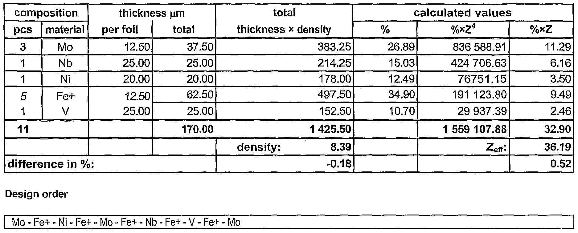
Table 19.
IP./F. type D 160 Medium
The 160 μm lead thickness in mg/cm2 181.60
Calculated thickness of the type 216.19 μm
Constant density of the type 8.40 g/cm3
Effective atomic number of the type 36.00 Zeff

Table 20.
IP./F. type D 200 Medium
The 200 μm lead thickness in mg/cm2 227.00
Calculated thickness of the type 270.00 μm
Constant density of the type 8.40 g/cm3
Effective atomic number of the type 36.00 Zeff

Table 21.
VPJF. type D 250 Medium
The 250 μm lead thickness in mg/cm2 283.75
Calculated thickness of the type 337.80 μm
Constant density of the type 8.40 g/cm3
Effective atomic number of the type 36.00 Zeff

Table 22.
Continuing this series the effective atomic number of all type D Zeff = 36.00 D 320 'Medium filter comes to fruition by overlaying of two pieces D 160 Medium filters 320 μm lead thickness in mg/cm2 363.20 Calculated thickness of the type 432.38 μm
Henceforth:
The D 400 Medium filter comes to fruition by overlaying of two pieces D 200 Medium filters
400 μm lead thickness in mg/cm2 454.00
Calculated thickness of the type 540.47 μm
The D 500 Medium filter comes to fruition by overlaying of two pieces D 250 Medium filters 500 μm lead thickness in mg/cm2 567.50
Calculated thickness of the type 675.59 μm
The D 640 Medium filter comes to fruition by overlaying of four pieces D 160 Medium filters 640 μm lead thickness in mg/cm2 726.40
Calculated thickness of the type 864.76 μm
The D 800 Medium filter comes to fruition by overlaying of four pieces D 200 Medium filters 800 μm lead thickness in mg/cm2 908.00
Calculated thickness of the type 1080.95 μm
The D 1000 Medium filter comes to fruition by overlaying of four pieces D 250 Medium filters 1000 μm lead thickness in mg/cm2 1135.00
Calculated thickness of the type 1351.19 μm
IP./F. type E 100 Medium
The 100 μm lead thickness in mg/cm2 113.50
Calculated thickness of the type 135.12 μm
Constant density of the type 8.40 g/cm3
Effective atomic number of the type 35.00 ZeK

Table 23.
IP./F. type E 125 Medium
The 125 μm lead thickness in mg/cm2 141,87
Calculated thickness of the type 168,90 μm
Constant density of the type 8.40 g/cm3
Effective atomic number of the type 35.00 Zetr

Table 24.
IP./F. type E 160 Medium
The 160 μm lead thickness in mg/cm2 181.60
Calculated thickness of the type 216.19 μm
Constant density of the type 8.40 g/cm3
Effective atomic number of the type 35.00 Zeff

Table 25.
IP./F. type E 200 Medium
The 200 μm lead thickness in mg/cm2 227.00
Calculated thickness of the type 270.24 μm
Constant density of the type 8.40 g/cm3
Effective atomic number of the type 35.00 Zen

Table 26.
IP./F. type E 250 Medium
The 250 μm lead thickness in mg/cm2 283.75 Calculated thickness of the type 337.80 μm Constant density of the type 8.40 g/cm3 Effective atomic number of the type • 35.00 Zeff

Table 27.
Continuing this series the effective atomic number of all type E Zeff = 35.00 and the E 320 Medium filter comes to fruition by overlaying of two pieces El 60 Medium filters 320 μm lead thickness in mg/cm2 363.20 Calculated thickness of the type 432.38 μm
Henceforth:
The E 400 Medium filter comes to fruition by overlaying of two pieces E 200 Medium filters
400 μm lead thickness in mg/cm2 454.00
Calculated thickness of the type 540.47 μm
The E 500 Medium filter comes to fruition by overlaying of two pieces E 250 Medium filters 500 μm lead thickness in mg/cm2 567.50
Calculated thickness of the type 675.59 μm
The E 640 Medium filter comes to fruition by overlaying of four pieces El 60 Medium filters 640 μm lead thickness in mg/cm2 726.40
Calculated thickness of the type 864.76 μm
The E 800 Medium filter comes to fruition by overlaying of four pieces E 200 Medium filters 800 μm lead thickness in mg/cm2 908.00
Calculated thickness of the type 1080.95 μm
The E 1000 Medium filter comes to fruition by overlaying of four pieces E 250 Medium filters 1000 μm lead thickness in mg/cm2 1135.00
Calculated thickness of the type 1351.19 μm
[P./F. type F 80 Soft
The 80 μm lead thickness in mg/cm2 90.80
Calculated thickness of the type 108.09 μm
Constant density of the type 8.40 g/cm3
Effective atomic number of the type 27.60 Zeff

Table 28.
IP./F. type F 100 Soft
The 100 μm lead thickness in mg/cm2 113,50
Calculated thickness of the type 135,12 μm
Constant density of the type 8.40 g/cm3
Effective atomic number of the type 27.60 Zeff

Table 29.
IP./F. type F 125 Soft
The 125 μm lead thickness in mg/cm2 141.87
Calculated thickness of the type 168.90 μm
Constant density of the type 8.40 g/cm3
Effective atomic number of the type 27.60 Zeff

Table 30.
IP./F. type F 160 Soft
The 160 μm lead thickness in mg/cm2 181,60
Calculated thickness of the type 216,19 μm
Constant density of the type 8.40 g/cm3
Effective atomic number of the type 27.60 Zeff

Table 31.
IP./F. type F 200 Soft
The 200 μm lead thickness in mg/cm2 227.00
Calculated thickness of the type 270.24 μm
Constant density of the type 8.40 g/cm3
Effective atomic number of the type 27.60 Zen

Table 32.
IP./F. type F 250 Soft
The 250 μm lead thickness in mg/cm2 283.75
Calculated thickness of the type 337.80 μm
Constant density of the type 8.40 g/cm3
Effective atomic number of the type 27.60 Zen

Table 33.
Continuing this series the effective atomic number of all type F Zeff = 27.60 and the F 320 Soft filter comes to fruition by overlaying of two pieces Fl 60 Sofi filters 320 μm lead thickness in mg/cm2 363.20
Calculated thickness of the type 432.38 μm
Henceforth:
The F 400 Soft filter comes to fruition by overlaying of two pieces F 200 Sofi filters
400 μm lead thickness in mg/cm 454.00 Calculated thickness of the type 540.47 μm
The F 500 Soft filter comes to fruition by overlaying of two pieces F 250 Soft filters
500 μm lead thickness in mg/cm 567.50 Calculated thickness of the type 675.59 μm
The F 640 Soft filter comes to fruition by overlaying of four pieces Fl 60 Soft filters 640 μm lead thickness in mg/cm2 726.40
Calculated thickness of the type 864.76 μm
The F 800 Soft filter comes to fruition by overlaying of four pieces F 200 Soft filters 800 μm lead thickness in mg/cm2 908.00
Calculated thickness of the type 1080.95 μm
The FlOOO Soft filter comes to fruition by overlaying of four pieces F 250 Soft filters
1000 μm lead thickness in mg/cm2 1135.OOCalculated thickness of the type
1351.19 μm
From the point of view of the patent the combination of the different type is allowed, e.g.: : ,,A"-,,D"-,,A", ,,D"-,,F"-,,D", etc. By this solution, the effective atomic number of the new device is changing. It is not necessary that the new device be symmetrically arranged the ,,A"-,,D", ,,D"-,,F", etc. arrangement is also possible. .
The device in the patent itself is not only image purifier/filter but it also affects favourably the contrast (image quality) therefore it is also recommended if there is no considerable radiation in the system or if there is considerable background and/or external radiation.
It should be noted that we constructed types ,,A" ,,C" and ,,D" - 17 pieces up to 400 μm Pb equivalent thickness - according to the ,,recommended product". The efficiency improvement of these devices - compared to the present status of the technique — minimum 25%.
The device in the patent realises the objective of the patent at all points. We do not deal with the incidentally applied plastic foils - mentioned before - because it is the subject of an other potential patent or production know-how.
Claims
Claims of the patent
1. Image purifier/filter device (henceforth: device) for improvement of the quality of image recorded on film used in the X-ray diagnostics and/or detector; first with filtering the scattered radiation - in the second place with improving the contrast and image quality — characterized with that the device consists of 4-400 pieces overlaid rolled metal sheets (metal foils) — made at least two different elements — each of them being 5-50 μm thick; the possible elements are Al, V, Cr, Fe, Ni, Nb, Mo, Ta, W and Pb; where each foil consists of at least in 80% the metals in the examples and/or their alloys; and the metal foils of the device are pieced together such a way that the average density of the devices' metal foils is 8,40 ± 1.6 g/cm3 (favourably 8,40 ± 0.3 g/cm3); and in addition depending on the implemented example its thickness in mg/cm2 is 64-2000; the effective atomic number is in the region between 25 and 75.
2. The device according to the 1st claim characterized that any foil of the device is pieced together from foil stripes and/or matrices.
3. The device according to the 1st claim characterized that more than one device may be made from identical metal.
4. The device according to the 1st claim characterized that the foils are placed on each other so that their rolling directions are perpendicular.
5. The device according to the 1st claim characterized that the foils are secured to each other by gluing.
6. The device according to the 1st claim characterized that the foils are secured to each other by laminating.
7. The device according to the 1st claim characterized that the foils are secured to each other by metallic coupling.
8. The device according to the 1st claim characterized that the foils are secured to each other by vacuum sealing.
9. The device according to the 1st claim characterized that the overlaid foils are fixed together at the edges.
10. The device according to the 1st claim characterized that it comprises in 80% rolled foils where the foils may be coated (metal vaporization, metal evaporating and galvanization).
11. The device according to the 1st and 10th claims characterized that it may be coated by painting and/or typographic and/or photographic way and/or by sintering.
12. The device according to the 1st, 10th and 11th claims characterized that there may be plastic and/or paper layers between the metal foils.
13. The device according to the 1st claim characterized that it is coated with external insulation and/or housing and/or coat.
15. The device according to the 1st, 10th and 11th claims characterized that any of the device's foil is fixed on a support.
16. The device according to the 1st, 10th and 11th claims characterized that the glues, plastics, papers and paints - as separating materials and/or coatings and/or supports and/or housings - mentioned in the 5th, 6th, 7th 10th, 11th, 12th, 13th, 14th, and 15th claims - are not taken into account to the device' average density and/or thickness (in mg/cm2) and/or total thickness up to the Pb equivalent thickness.
Applications Claiming Priority (2)
| Application Number | Priority Date | Filing Date | Title |
|---|---|---|---|
| HU0800182A HUP0800182A2 (en) | 2008-03-21 | 2008-03-21 | Picture cleaner/filter device for scattered x-ray/gamma radiation |
| HUP0800182 | 2008-03-21 |
Publications (1)
| Publication Number | Publication Date |
|---|---|
| WO2009115853A1 true WO2009115853A1 (en) | 2009-09-24 |
Family
ID=89988153
Family Applications (1)
| Application Number | Title | Priority Date | Filing Date |
|---|---|---|---|
| PCT/HU2009/000028 WO2009115853A1 (en) | 2008-03-21 | 2009-03-23 | Device for image purifier/filter scattered x-ray/gamma radiation |
Country Status (2)
| Country | Link |
|---|---|
| HU (1) | HUP0800182A2 (en) |
| WO (1) | WO2009115853A1 (en) |
Citations (3)
| Publication number | Priority date | Publication date | Assignee | Title |
|---|---|---|---|---|
| AU540580B3 (en) * | 1984-09-14 | 1984-11-29 | Intico (S.A.) Pty. Ltd. | Flaw detection |
| EP0220937A2 (en) * | 1984-11-05 | 1987-05-06 | Péter Teleki | Structure for shielding X-ray and gamma radiation |
| WO1990006582A1 (en) * | 1988-11-28 | 1990-06-14 | Teleki Peter | Structure for influencing the effect of x-ray or gamma radiation on a target sensitive to the radiation |
-
2008
- 2008-03-21 HU HU0800182A patent/HUP0800182A2/en unknown
-
2009
- 2009-03-23 WO PCT/HU2009/000028 patent/WO2009115853A1/en active Application Filing
Patent Citations (3)
| Publication number | Priority date | Publication date | Assignee | Title |
|---|---|---|---|---|
| AU540580B3 (en) * | 1984-09-14 | 1984-11-29 | Intico (S.A.) Pty. Ltd. | Flaw detection |
| EP0220937A2 (en) * | 1984-11-05 | 1987-05-06 | Péter Teleki | Structure for shielding X-ray and gamma radiation |
| WO1990006582A1 (en) * | 1988-11-28 | 1990-06-14 | Teleki Peter | Structure for influencing the effect of x-ray or gamma radiation on a target sensitive to the radiation |
Also Published As
| Publication number | Publication date |
|---|---|
| HUP0800182A2 (en) | 2010-01-28 |
| HU0800182D0 (en) | 2008-05-28 |
Similar Documents
| Publication | Publication Date | Title |
|---|---|---|
| EP2102871B1 (en) | Beam filter, particularly for x-rays, that does not change the beam's spectral composition | |
| JP6694890B2 (en) | Scattered ray grid, layer plate and method for manufacturing layer plate | |
| EP0426836B1 (en) | X-ray grid for medical radiography and method of making and using same | |
| CN102782769A (en) | A multi-layer light-weight garment material with low radiation buildup providing scattered-radiation shielding | |
| JP5648965B2 (en) | Apparatus for adjusting spatial intensity distribution of radiation and spatial distribution of energy, and X-ray generator and radiation detector using the adjusting apparatus | |
| KR20020026433A (en) | Anti-scatter grid, method, and apparatus for forming same | |
| US11744536B2 (en) | Monochromatic x-ray imaging systems and methods | |
| JP2015092953A (en) | Radiographic apparatus and radiographic imaging system | |
| US20130287177A1 (en) | Method and apparatus for transmission of fluorescence x-ray radiation using a multilayer x-ray target | |
| CA1250062A (en) | Radiation reduction filter for use in medical diagnosis | |
| JP5208224B2 (en) | Radiography apparatus and radiation imaging system | |
| JP3741613B2 (en) | High energy X-ray imaging apparatus and method | |
| WO2009115853A1 (en) | Device for image purifier/filter scattered x-ray/gamma radiation | |
| JP6763205B2 (en) | Laminated scintillator panel | |
| US5321272A (en) | X-ray beam stop | |
| Rutherford et al. | XXXIV. Spectrum of the β rays excited by γ rays | |
| EP0989566B1 (en) | Radiation intensifying screen, radiation receptor and radiation inspection device therewith | |
| RU2171979C2 (en) | Antidissipating x-ray raster (alternatives) | |
| JP2016026289A (en) | Mo COLLIMATOR AND X-RAY DETECTOR, X-RAY INSPECTION APPARATUS AND CT APPARATUS USING THE SAME | |
| JP2013098168A (en) | Transmission type x-ray tube and reflection type x-ray tube | |
| KR101909939B1 (en) | Filter for reducing low energy x-ray, x-ray tube comprising the filter and x-ray system comprising the filter | |
| JPH03502489A (en) | Structures that influence the effect of X-rays or gamma rays on radiation-sensitive targets | |
| US20080292060A1 (en) | X-ray imaging cassette for use in radiotherapy | |
| KR102034863B1 (en) | Filter for reducing low energy bandwidth x-ray, x-ray tube comprising the filter, and x-ray apparatus comprising the filter | |
| Prieto-Pena et al. | Radiation characterisation and dosimetric measurements of a femtosecond pulsed laser ablation system |
Legal Events
| Date | Code | Title | Description |
|---|---|---|---|
| 121 | Ep: the epo has been informed by wipo that ep was designated in this application |
Ref document number: 09722283 Country of ref document: EP Kind code of ref document: A1 |
|
| NENP | Non-entry into the national phase |
Ref country code: DE |
|
| 122 | Ep: pct application non-entry in european phase |
Ref document number: 09722283 Country of ref document: EP Kind code of ref document: A1 |