WO2009113255A1 - Plasma display device - Google Patents
Plasma display device Download PDFInfo
- Publication number
- WO2009113255A1 WO2009113255A1 PCT/JP2009/000839 JP2009000839W WO2009113255A1 WO 2009113255 A1 WO2009113255 A1 WO 2009113255A1 JP 2009000839 W JP2009000839 W JP 2009000839W WO 2009113255 A1 WO2009113255 A1 WO 2009113255A1
- Authority
- WO
- WIPO (PCT)
- Prior art keywords
- voltage
- electrode
- discharge
- plasma display
- pdp
- Prior art date
Links
Images


Classifications
-
- G—PHYSICS
- G09—EDUCATION; CRYPTOGRAPHY; DISPLAY; ADVERTISING; SEALS
- G09G—ARRANGEMENTS OR CIRCUITS FOR CONTROL OF INDICATING DEVICES USING STATIC MEANS TO PRESENT VARIABLE INFORMATION
- G09G3/00—Control arrangements or circuits, of interest only in connection with visual indicators other than cathode-ray tubes
- G09G3/20—Control arrangements or circuits, of interest only in connection with visual indicators other than cathode-ray tubes for presentation of an assembly of a number of characters, e.g. a page, by composing the assembly by combination of individual elements arranged in a matrix no fixed position being assigned to or needed to be assigned to the individual characters or partial characters
- G09G3/22—Control arrangements or circuits, of interest only in connection with visual indicators other than cathode-ray tubes for presentation of an assembly of a number of characters, e.g. a page, by composing the assembly by combination of individual elements arranged in a matrix no fixed position being assigned to or needed to be assigned to the individual characters or partial characters using controlled light sources
- G09G3/28—Control arrangements or circuits, of interest only in connection with visual indicators other than cathode-ray tubes for presentation of an assembly of a number of characters, e.g. a page, by composing the assembly by combination of individual elements arranged in a matrix no fixed position being assigned to or needed to be assigned to the individual characters or partial characters using controlled light sources using luminous gas-discharge panels, e.g. plasma panels
- G09G3/288—Control arrangements or circuits, of interest only in connection with visual indicators other than cathode-ray tubes for presentation of an assembly of a number of characters, e.g. a page, by composing the assembly by combination of individual elements arranged in a matrix no fixed position being assigned to or needed to be assigned to the individual characters or partial characters using controlled light sources using luminous gas-discharge panels, e.g. plasma panels using AC panels
- G09G3/291—Control arrangements or circuits, of interest only in connection with visual indicators other than cathode-ray tubes for presentation of an assembly of a number of characters, e.g. a page, by composing the assembly by combination of individual elements arranged in a matrix no fixed position being assigned to or needed to be assigned to the individual characters or partial characters using controlled light sources using luminous gas-discharge panels, e.g. plasma panels using AC panels controlling the gas discharge to control a cell condition, e.g. by means of specific pulse shapes
-
- H—ELECTRICITY
- H01—ELECTRIC ELEMENTS
- H01J—ELECTRIC DISCHARGE TUBES OR DISCHARGE LAMPS
- H01J11/00—Gas-filled discharge tubes with alternating current induction of the discharge, e.g. alternating current plasma display panels [AC-PDP]; Gas-filled discharge tubes without any main electrode inside the vessel; Gas-filled discharge tubes with at least one main electrode outside the vessel
- H01J11/10—AC-PDPs with at least one main electrode being out of contact with the plasma
- H01J11/12—AC-PDPs with at least one main electrode being out of contact with the plasma with main electrodes provided on both sides of the discharge space
-
- G—PHYSICS
- G09—EDUCATION; CRYPTOGRAPHY; DISPLAY; ADVERTISING; SEALS
- G09G—ARRANGEMENTS OR CIRCUITS FOR CONTROL OF INDICATING DEVICES USING STATIC MEANS TO PRESENT VARIABLE INFORMATION
- G09G3/00—Control arrangements or circuits, of interest only in connection with visual indicators other than cathode-ray tubes
- G09G3/20—Control arrangements or circuits, of interest only in connection with visual indicators other than cathode-ray tubes for presentation of an assembly of a number of characters, e.g. a page, by composing the assembly by combination of individual elements arranged in a matrix no fixed position being assigned to or needed to be assigned to the individual characters or partial characters
- G09G3/22—Control arrangements or circuits, of interest only in connection with visual indicators other than cathode-ray tubes for presentation of an assembly of a number of characters, e.g. a page, by composing the assembly by combination of individual elements arranged in a matrix no fixed position being assigned to or needed to be assigned to the individual characters or partial characters using controlled light sources
- G09G3/28—Control arrangements or circuits, of interest only in connection with visual indicators other than cathode-ray tubes for presentation of an assembly of a number of characters, e.g. a page, by composing the assembly by combination of individual elements arranged in a matrix no fixed position being assigned to or needed to be assigned to the individual characters or partial characters using controlled light sources using luminous gas-discharge panels, e.g. plasma panels
- G09G3/288—Control arrangements or circuits, of interest only in connection with visual indicators other than cathode-ray tubes for presentation of an assembly of a number of characters, e.g. a page, by composing the assembly by combination of individual elements arranged in a matrix no fixed position being assigned to or needed to be assigned to the individual characters or partial characters using controlled light sources using luminous gas-discharge panels, e.g. plasma panels using AC panels
- G09G3/291—Control arrangements or circuits, of interest only in connection with visual indicators other than cathode-ray tubes for presentation of an assembly of a number of characters, e.g. a page, by composing the assembly by combination of individual elements arranged in a matrix no fixed position being assigned to or needed to be assigned to the individual characters or partial characters using controlled light sources using luminous gas-discharge panels, e.g. plasma panels using AC panels controlling the gas discharge to control a cell condition, e.g. by means of specific pulse shapes
- G09G3/293—Control arrangements or circuits, of interest only in connection with visual indicators other than cathode-ray tubes for presentation of an assembly of a number of characters, e.g. a page, by composing the assembly by combination of individual elements arranged in a matrix no fixed position being assigned to or needed to be assigned to the individual characters or partial characters using controlled light sources using luminous gas-discharge panels, e.g. plasma panels using AC panels controlling the gas discharge to control a cell condition, e.g. by means of specific pulse shapes for address discharge
- G09G3/2932—Addressed by writing selected cells that are in an OFF state
-
- H—ELECTRICITY
- H01—ELECTRIC ELEMENTS
- H01J—ELECTRIC DISCHARGE TUBES OR DISCHARGE LAMPS
- H01J11/00—Gas-filled discharge tubes with alternating current induction of the discharge, e.g. alternating current plasma display panels [AC-PDP]; Gas-filled discharge tubes without any main electrode inside the vessel; Gas-filled discharge tubes with at least one main electrode outside the vessel
- H01J11/20—Constructional details
- H01J11/34—Vessels, containers or parts thereof, e.g. substrates
- H01J11/40—Layers for protecting or enhancing the electron emission, e.g. MgO layers
-
- G—PHYSICS
- G09—EDUCATION; CRYPTOGRAPHY; DISPLAY; ADVERTISING; SEALS
- G09G—ARRANGEMENTS OR CIRCUITS FOR CONTROL OF INDICATING DEVICES USING STATIC MEANS TO PRESENT VARIABLE INFORMATION
- G09G3/00—Control arrangements or circuits, of interest only in connection with visual indicators other than cathode-ray tubes
- G09G3/20—Control arrangements or circuits, of interest only in connection with visual indicators other than cathode-ray tubes for presentation of an assembly of a number of characters, e.g. a page, by composing the assembly by combination of individual elements arranged in a matrix no fixed position being assigned to or needed to be assigned to the individual characters or partial characters
- G09G3/22—Control arrangements or circuits, of interest only in connection with visual indicators other than cathode-ray tubes for presentation of an assembly of a number of characters, e.g. a page, by composing the assembly by combination of individual elements arranged in a matrix no fixed position being assigned to or needed to be assigned to the individual characters or partial characters using controlled light sources
- G09G3/28—Control arrangements or circuits, of interest only in connection with visual indicators other than cathode-ray tubes for presentation of an assembly of a number of characters, e.g. a page, by composing the assembly by combination of individual elements arranged in a matrix no fixed position being assigned to or needed to be assigned to the individual characters or partial characters using controlled light sources using luminous gas-discharge panels, e.g. plasma panels
- G09G3/288—Control arrangements or circuits, of interest only in connection with visual indicators other than cathode-ray tubes for presentation of an assembly of a number of characters, e.g. a page, by composing the assembly by combination of individual elements arranged in a matrix no fixed position being assigned to or needed to be assigned to the individual characters or partial characters using controlled light sources using luminous gas-discharge panels, e.g. plasma panels using AC panels
- G09G3/296—Driving circuits for producing the waveforms applied to the driving electrodes
Definitions
- the present invention relates to a plasma display apparatus using a plasma display panel as a display device.
- Plasma display panels are capable of realizing high definition and large screens, so 65-inch class televisions have been commercialized.
- PDP has been applied to high-definition televisions having more than twice the number of scanning lines as compared with the conventional NTSC system, and PDP containing no lead component is required in consideration of environmental problems.
- the PDP is basically composed of a front plate and a back plate.
- the front plate is a glass substrate made of sodium borosilicate glass by a float method, a display electrode composed of a striped transparent electrode and a bus electrode formed on one main surface of the glass substrate, and a display electrode A dielectric layer that covers and acts as a capacitor, and a protective layer made of magnesium oxide (MgO) formed on the dielectric layer.
- the back plate is a glass substrate, stripe-shaped data electrodes formed on one main surface thereof, a base dielectric layer covering the data electrodes, a partition formed on the base dielectric layer, and a partition It is comprised with the fluorescent substance layer which light-emits each in red, green, and blue formed in between.
- the PDP is held by holding the PDP on the front side of a chassis member made of a metal plate, and arranging a drive circuit block for driving the PDP on the back side of the chassis member. It comprises, and this PDP module is accommodated in a case (refer patent document 1).
- the plasma display device of the present invention includes a plasma display panel and a drive circuit.
- the plasma display panel includes a front plate having a plurality of display electrodes and a back plate having a plurality of data electrodes arranged in a direction intersecting the display electrodes.
- a plurality of discharge cells are formed by disposing the front plate and the back plate so as to form a discharge space therebetween.
- the drive circuit applies a drive voltage to the display electrodes and data electrodes of the plasma display panel.
- Each field is composed of a plurality of subfields, and each subfield includes an address period for selecting a discharge cell to be discharged and a sustain period for performing a sustain discharge in the discharge cell selected in the address period. Have.
- a base film is formed on the dielectric layer covering the display electrodes, and a plurality of crystal particles made of metal oxide are attached to the base film so as to be distributed over the entire surface.
- the drive circuit is configured to apply a voltage having a pulse width of 1 ⁇ s or less to the data electrode during the write period.
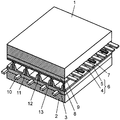
- FIG. 1 is a perspective view showing the structure of a PDP used in a plasma display device according to an embodiment of the present invention.
- FIG. 2 is an electrode array diagram of the PDP.
- FIG. 3 is a block circuit diagram of the plasma display device in accordance with the exemplary embodiment of the present invention.
- FIG. 4 is a drive waveform diagram of the apparatus.
- FIG. 5 is an exploded perspective view showing the overall configuration of the plasma display device according to the embodiment of the present invention.
- FIG. 6 is a plan view of the PDP module portion of the apparatus as viewed from the back side.
- FIG. 7A is a plan view of the PDP of the PDP module as seen from the back side.
- FIG. 7B is a plan view of the PDP of the PDP module as viewed from the front side.
- FIG. 1 is a perspective view showing the structure of a PDP used in a plasma display device according to an embodiment of the present invention.
- FIG. 2 is an electrode array diagram of the PDP.
- FIG. 8 is an enlarged plan view showing a main part of the PDP module.
- FIG. 9 is a cross-sectional view showing the configuration of the front plate of the PDP of the plasma display device in accordance with the exemplary embodiment of the present invention.
- FIG. 10 is an enlarged view for explaining aggregated particles in the protective layer of the front plate.
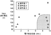
- FIG. 11 is a characteristic diagram showing the examination results of the electron emission performance and the Vscn lighting voltage in the PDP in the experimental results conducted to explain the effects of the embodiment of the present invention.
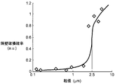
- FIG. 12 is a characteristic diagram showing the results of cathodoluminescence measurement of crystal particles.
- FIG. 13 is a characteristic diagram showing the relationship between the crystal grain size and the electron emission performance.
- FIG. 14 is a characteristic diagram showing the relationship between the grain size of crystal grains and the incidence of partition wall breakage.
- FIG. 15 is a characteristic diagram showing an example of the particle size distribution of crystal particles in the PDP according to the embodiment of the present invention.
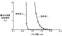
- FIG. 16 is a characteristic diagram showing the relationship between the pulse width of the pulse voltage applied to the data electrode and the address discharge failure probability in the PDP according to the embodiment of the present invention.
- FIG. 1 is a perspective view showing the structure of a PDP in a plasma display apparatus according to an embodiment of the present invention.
- a front plate 1 made of a front glass substrate and a back plate 2 made of a back glass substrate are arranged to face each other.
- the outer periphery of the PDP is hermetically sealed with a sealing material made of glass frit or the like.
- a discharge space 3 formed between the front plate 1 and the back plate 2 is filled with a discharge gas such as Ne and Xe at a pressure of 400 Torr to 600 Torr.
- a pair of strip-shaped display electrodes 6 composed of scanning electrodes 4 and sustaining electrodes 5 and black stripes (light shielding layers) 7 are arranged in a plurality of rows in parallel with each other.
- a dielectric layer 8 that functions as a capacitor is formed on the front glass substrate so as to cover the display electrode 6 and the light shielding layer 7. Further, a protective layer 9 made of magnesium oxide (MgO) or the like is formed on the surface of the dielectric layer 8.
- MgO magnesium oxide
- a plurality of strip-like data electrodes 10 are arranged in parallel to each other in a direction intersecting with the scan electrodes 4 and the sustain electrodes 5 of the front plate 1.
- the data electrode 10 is covered with the base dielectric layer 11.
- a partition wall 12 having a predetermined height is formed on the underlying dielectric layer 11 between the data electrodes 10 to divide the discharge space 3.
- a phosphor layer 13 that emits red, green, and blue light by ultraviolet rays is sequentially applied to the grooves between the barrier ribs 12.
- a discharge cell is formed at a position where the scan electrode 4 and the sustain electrode 5 intersect the data electrode 10, and a discharge cell having red, green, and blue phosphor layers 13 arranged in the direction of the display electrode 6 is a pixel for color display. become.
- FIG. 2 is an electrode array diagram of the PDP.
- scan electrodes SC1 to SCn scan electrode 4 in FIG. 1
- n sustain electrodes SU1 to SUn FIG. 1 extended in the row direction.
- the sustain electrodes 5) are arranged.
- M ⁇ n discharge cells are formed in the discharge space.
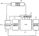
- FIG. 3 is a circuit block diagram of a plasma display device using this PDP.
- the plasma display device includes a PDP 14, an image signal processing circuit 15, a data electrode drive circuit 16, a scan electrode drive circuit 17, a sustain electrode drive circuit 18, a timing generation circuit 19, and a power supply circuit (not shown).
- the image signal processing circuit 15 converts the image signal sig into image data for each subfield.
- the data electrode driving circuit 16 converts the image data for each subfield into signals corresponding to the data electrodes D1 to Dm, and drives the data electrodes D1 to Dm.
- the timing generation circuit 19 generates various timing signals based on the horizontal synchronization signal H and the vertical synchronization signal V, and supplies them to each drive circuit block.
- Scan electrode drive circuit 17 supplies a drive voltage waveform to scan electrodes SC1 to SCn based on the timing signal.
- Sustain electrode drive circuit 18 supplies a drive voltage waveform to sustain electrodes SU1 to SUn based on the timing signal.
- the plasma display device includes the front plate 1 having the plurality of display electrodes 6 and the back plate 2 having the plurality of data electrodes 10 arranged in a direction intersecting the display electrodes 6.
- a driving voltage is applied to the PDP 14 in which a plurality of discharge cells are formed by facing the front plate 1 and the back plate 2 so as to form a discharge space 3 therebetween, and to the display electrode 6 and the data electrode 10 of the PDP 14.
- a scan electrode drive circuit 17 and a sustain electrode drive circuit 18 are provided as drive circuits for this purpose.
- FIG. 4 is a diagram showing drive voltage waveforms applied to the respective electrodes of the PDP.
- one field is composed of a plurality of subfields.
- Each subfield has an initialization period, an address period for selecting a discharge cell to be discharged, and a sustain period in which a sustain discharge is performed in the discharge cells selected in this address period.
- the data electrodes D1 to Dm and the sustain electrodes SU1 to SUn are held at 0 (V). Then, a ramp voltage that gradually rises from voltage Vi1 (V) that is equal to or lower than the discharge start voltage to voltage Vi2 (V) that exceeds the discharge start voltage is applied to scan electrodes SC1 to SCn. Then, the first weak setup discharge is caused in all the discharge cells. As a result, negative wall voltage is stored on scan electrodes SC1 to SCn, and positive wall voltage is stored on sustain electrodes SU1 to SUn and data electrodes D1 to Dm.
- the wall voltage on the electrode refers to a voltage generated by wall charges accumulated on the dielectric layer or the phosphor layer covering the electrode.
- sustain electrodes SU1 to SUn are maintained at positive voltage Vh (V). Then, a ramp voltage that gradually decreases from voltage Vi3 (V) to voltage Vi4 (V) is applied to scan electrodes SC1 to SCn. Then, the second weak initializing discharge is caused in all the discharge cells. As a result, the wall voltage between scan electrodes SC1 to SCn and sustain electrodes SU1 to SUn is weakened, and the wall voltage on data electrodes D1 to Dm is also adjusted to a value suitable for the write operation.
- scan electrodes SC1 to SCn are temporarily held at Vc (V).
- a positive write pulse voltage Vd (V) having a pulse width Td is applied to m).
- Vd ⁇ Va the externally applied voltage
- the voltage at the intersection of the data electrode Dk and the scan electrode SC1 exceeds the discharge start voltage.
- An address discharge occurs between data electrode Dk and scan electrode SC1 and between sustain electrode SU1 and scan electrode SC1. Then, a positive wall voltage is accumulated on scan electrode SC1 of this discharge cell, a negative wall voltage is accumulated on sustain electrode SU1, and a negative wall voltage is also accumulated on data electrode Dk.
- the address operation is performed in which the address discharge is caused in the discharge cells to be displayed in the first row and the wall voltage is accumulated on each electrode.
- the voltage at the intersection of the data electrodes D1 to Dm to which the address pulse voltage Vd (V) is not applied and the scan electrode SC1 does not exceed the discharge start voltage, so that address discharge does not occur.
- the above address operation is sequentially performed until the discharge cell in the nth row, and the address period ends.
- the sustain discharge continues in the discharge cells that have caused the address discharge in the address period by alternately applying the number of sustain pulses corresponding to the luminance weight to the scan electrodes SC1 to SCn and the sustain electrodes SU1 to SUn. Done. Thus, the maintenance operation in the maintenance period is completed.
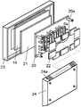
- FIG. 5 shows an example of the overall configuration of a plasma display device incorporating the PDP having the structure described above.
- FIG. 6 shows an example of the arrangement of the drive circuit blocks of the PDP module as viewed from the back side.
- FIGS. 7A and 7B show plan views of the PDP as viewed from the back plate side and the front plate side. Moreover, the principal part of the PDP module seen from the back side is shown in FIG.
- the chassis member 20 as a holding plate also serves as a metal heat sink.
- the PDP 14 is held by adhering the heat dissipation sheet 21 between the PDP 14 and the chassis member 20 with an adhesive or the like.
- a plurality of drive circuit blocks 22 for displaying and driving the PDP 14 are arranged on the rear side of the chassis member 20. These constitute a PDP module.
- the drive circuit board 22 is attached to the pins 20a provided on the chassis member 20 with screws or the like.
- the PDP module having such a structure includes a front protective cover 23 disposed on the front side of the PDP 14 and a metal back cover 24 disposed on the rear side of the chassis member 20.
- the plasma display device is completed by being housed in the body.
- the back cover 24 is provided with a plurality of vent holes 24a for releasing heat generated by the module to the outside.
- FIG. 6 the panel portion of the PDP and the PDP module will be described in detail with reference to FIG. 6, FIG. 7A, 7B, and FIG.
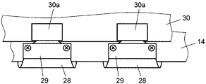
- the PDP 14 has electrode terminal portions 14 a connected to the scanning electrodes 4 and the sustain electrodes 5 constituting the plurality of display electrodes 6 at opposite side ends of the front plate 1. 14b is provided. In addition, an electrode terminal portion 14 c connected to the plurality of data electrodes 10 is provided at a lower end portion which is one end portion of the back plate 2.
- flexible wiring boards 25 as wiring boards for display electrodes connected to the electrode lead-out portions 14 a and 14 b of the scan electrode 4 and the sustain electrode 5 are provided at both side ends of the PDP 14. ing.
- the flexible wiring board 25 is routed to the back side through the outer periphery of the chassis member 20.
- the flexible wiring board 25 is connected to the drive circuit board 26 of the scan electrode drive circuit 17 and the drive circuit board 27 of the sustain electrode drive circuit 18 via connectors.
- a plurality of flexible wiring boards 28 as wiring boards for the data electrodes 10 connected to the electrode lead portions 14 c of the data electrodes 10 are provided at the lower end of the PDP 14. These flexible wiring boards 28 are routed to the back side through the outer periphery of the chassis member 20.
- the flexible wiring board 28 is electrically connected to each of a plurality of data drivers 29 of the data electrode driving circuit 16 for applying a driving voltage to the data electrodes 10.
- the flexible wiring board 28 is electrically connected to the drive circuit board 30 of the data electrode drive circuit 16 disposed at the lower position on the back side of the chassis member 20.
- the data driver 29 is configured by arranging a semiconductor chip on a heat sink.
- the data driver 29 has a structure in which each of the plurality of electrode pads of the semiconductor chip is connected to the wiring pattern of the flexible wiring board 28.
- the drive circuit board 30 is provided with a connector 30 a for connecting the flexible wiring board 28.
- the control circuit board 31 receives image data from the PDP 14 based on a video signal sent from an input signal circuit block 32 having an input terminal portion to which a connection cable for connecting to an external device such as a television tuner is detachably connected. Is converted into an image data signal corresponding to the number of pixels and supplied to the drive circuit board 30 of the data electrode drive circuit 16. Further, the control circuit board 31 generates a discharge control timing signal and supplies it to the drive circuit board 26 of the scan electrode drive circuit 17 and the drive circuit board 27 of the sustain electrode drive circuit 18, respectively, and display drive control such as gradation control. Is to do.
- the control circuit board 31 is disposed substantially at the center of the chassis member 20.
- the power supply block 33 supplies a voltage to each circuit block. Similar to the control circuit board 31, the power supply block 33 is disposed at a substantially central portion of the chassis member 20. A commercial power supply voltage is supplied to the power supply block 33 through a connector to which a power supply cable (not shown) is attached. In addition, a cooling fan (not shown) is disposed at an angle in the vicinity of the drive circuit board. The drive circuit board is cooled by the wind sent from the cooling fan.
- FIG. 9 is a cross-sectional view showing the configuration of the front plate 1 of the PDP 14 in the present invention.
- the front plate 1 is formed by patterning a display electrode 6 including a scan electrode 4 and a sustain electrode 5 and a light shielding layer 7 on a front glass substrate manufactured by a float method or the like.
- Scan electrode 4 and sustain electrode 5 are each composed of transparent electrodes 4a and 5a made of indium tin oxide (ITO), tin oxide (SnO2), and the like, and metal bus electrodes 4b and 5b formed on transparent electrodes 4a and 5a. It is configured.
- the metal bus electrodes 4b and 5b are used for the purpose of imparting conductivity in the longitudinal direction of the transparent electrodes 4a and 5a, respectively, and are formed of a conductive material mainly composed of a silver (Ag) material.
- the dielectric layer 8 includes a first dielectric layer 81 provided on the front glass substrate so as to cover the transparent electrodes 4a and 5a, the metal bus electrodes 4b and 5b, and the light shielding layer 7, and a first dielectric
- the second dielectric layer 82 formed on the layer 81 has at least two layers.
- the protective layer 9 is formed on the second dielectric layer 82.
- the protective layer 9 is composed of a base film 91 formed on the dielectric layer 8 and agglomerated particles 92 attached on the base film 91.
- first dielectric layer 81 and the second dielectric layer 82 constituting the dielectric layer 8 of the front plate 1 will be described in detail.
- the dielectric material of the first dielectric layer 81 is composed of the following material composition. That is, it contains 20% to 40% by weight of bismuth oxide (Bi 2 O 3 ), and 0.5% by weight of at least one selected from calcium oxide (CaO), strontium oxide (SrO), and barium oxide (BaO). -12 wt%, 0.1 wt% to 7 wt% of at least one selected from molybdenum oxide (MoO 3 ), tungsten oxide (WO 3 ), cerium oxide (CeO 2 ) and manganese dioxide (MnO 2 ) It is out.
- bismuth oxide Bi 2 O 3
- BaO barium oxide
- MoO 3 molybdenum oxide
- WO 3 tungsten oxide
- CeO 2 cerium oxide
- MnO 2 manganese dioxide
- molybdenum oxide MoO 3
- tungsten oxide WO 3
- cerium oxide CeO 2
- manganese dioxide MnO 2
- copper oxide CuO
- chromium oxide Cr 2 O 3
- cobalt oxide At least one selected from (Co 2 O 3 ), vanadium oxide (V 2 O 7 ), and antimony oxide (Sb 2 O 3 ) may be contained in an amount of 0.1 wt% to 7 wt%.
- zinc oxide (ZnO) is contained in an amount of 0 to 40% by weight, boron oxide (B 2 O 3 ) in an amount of 0 to 35% by weight, and silicon oxide (SiO 2 ) in an amount of 0 to 4% by weight.
- boron oxide (B 2 O 3 ) in an amount of 0 to 35% by weight
- silicon oxide (SiO 2 ) in an amount of 0 to 4% by weight.
- 15 wt%, aluminum oxide (Al 2 O 3) such as from 0% to 10% by weight, may contain a material composition containing no lead component, there is no particular limitation on the content of these material compositions.
- a dielectric material powder is prepared by pulverizing a dielectric material composed of these composition components with a wet jet mill or a ball mill so that the average particle diameter is 0.5 ⁇ m to 2.5 ⁇ m. Next, 55 wt% to 70 wt% of the dielectric material powder and 30 wt% to 45 wt% of the binder component are well kneaded with three rolls to obtain a first dielectric layer paste for die coating or printing. Make it.
- the binder component is ethyl cellulose, terpineol containing 1% to 20% by weight of acrylic resin, or butyl carbitol acetate.
- the paste if necessary, at least one of dioctyl phthalate, dibutyl phthalate, triphenyl phosphate and tributyl phosphate is added as a plasticizer, and glycerol monooleate and sorbitan sesquioleate as a dispersant.
- at least one of homogenol (a product name of Kao Corporation) and a phosphoric ester of an alkylallyl group may be added to improve printability.
- the front glass substrate is printed by a die coating method or a screen printing method so as to cover the display electrode 6 and dried, and then, a temperature slightly higher than the softening point of the dielectric material is 575 ° C. Bake at ⁇ 590 ° C.
- the dielectric material of the second dielectric layer 82 is composed of the following material composition. That is, bismuth oxide (Bi 2 O 3 ) is contained in an amount of 11 to 20% by weight, and at least one selected from calcium oxide (CaO), strontium oxide (SrO), and barium oxide (BaO) is 1.6. It contains from 0.1% to 7% by weight of at least one selected from molybdenum oxide (MoO 3 ), tungsten oxide (WO 3 ), and cerium oxide (CeO 2 ).
- MoO 3 molybdenum oxide
- tungsten oxide WO 3
- cerium oxide CeO 2
- copper oxide CuO
- chromium oxide Cr 2 O 3
- cobalt oxide Co 2 O 3
- At least one selected from vanadium oxide (V 2 O 7 ), antimony oxide (Sb 2 O 3 ), and manganese oxide (MnO 2 ) may be contained in an amount of 0.1 wt% to 7 wt%.
- zinc oxide (ZnO) is contained in an amount of 0 to 40% by weight, boron oxide (B 2 O 3 ) in an amount of 0 to 35% by weight, and silicon oxide (SiO 2 ) in an amount of 0 to 4% by weight.
- boron oxide (B 2 O 3 ) in an amount of 0 to 35% by weight
- silicon oxide (SiO 2 ) in an amount of 0 to 4% by weight.
- 15 wt%, aluminum oxide (Al 2 O 3) such as from 0% to 10% by weight, may contain a material composition containing no lead component, there is no particular limitation on the content of these material compositions.
- a dielectric material powder is prepared by pulverizing a dielectric material composed of these composition components with a wet jet mill or a ball mill so that the average particle diameter is 0.5 ⁇ m to 2.5 ⁇ m. Next, 55 wt% to 70 wt% of the dielectric material powder and 30 wt% to 45 wt% of the binder component are well kneaded with three rolls to form a second dielectric layer paste for die coating or printing. Make it.
- the binder component is ethyl cellulose, terpineol containing 1% to 20% by weight of acrylic resin, or butyl carbitol acetate.
- dioctyl phthalate, dibutyl phthalate, triphenyl phosphate and tributyl phosphate are added to the paste as needed, and glycerol monooleate, sorbitan sesquioleate, homogenol (Kao Corporation) as a dispersant.
- the printability may be improved by adding a phosphoric ester of an alkyl allyl group or the like.
- this second dielectric layer paste printing is performed on the first dielectric layer 81 by a screen printing method or a die coating method, followed by drying. Thereafter, a temperature slightly higher than the softening point of the dielectric material is 550 ° C. to 590 ° C. Bake at °C.
- the film thickness of the dielectric layer 8 is preferably 41 ⁇ m or less in order to secure the visible light transmittance by combining the first dielectric layer 81 and the second dielectric layer 82.
- the bismuth oxide (Bi 2 O 3 ) is 11% by weight or less in the second dielectric layer 82, coloring is less likely to occur, but bubbles are likely to be generated in the second dielectric layer 82, which is not preferable. On the other hand, if it exceeds 40% by weight, coloring tends to occur, which is not preferable for the purpose of increasing the transmittance.
- the thickness of the dielectric layer 8 is set to 41 ⁇ m or less, the first dielectric layer 81 is set to 5 ⁇ m to 15 ⁇ m, and the second dielectric layer 82 is set to 20 ⁇ m to 36 ⁇ m. Yes.
- the PDP manufactured in this manner has little coloring phenomenon (yellowing) of the front glass substrate even when a silver (Ag) material is used for the display electrode 6, and bubbles are generated in the dielectric layer 8. There is no. Therefore, the dielectric layer 8 excellent in withstand voltage performance can be realized.
- the dielectric layer 8 of the PDP 14 in the embodiment of the present invention suppresses yellowing and bubble generation in the first dielectric layer 81 in contact with the metal bus electrodes 4b and 5b made of silver (Ag) material. .
- the dielectric layer 8 achieves high light transmittance by the second dielectric layer 82 provided on the first dielectric layer 81. As a result, it is possible to realize a PDP having a high transmittance with very few bubbles and yellowing as the entire dielectric layer 8.
- a protective layer 9 is formed as shown in FIG.
- a base film 91 made of MgO containing Al as an impurity is formed on the dielectric layer 8.
- agglomerated particles 92 in which a plurality of MgO crystal particles 92a, which are metal oxides, are agglomerated are dispersed on the base film 91 in a discrete manner.
- the protective layer 9 is configured by adhering the plurality of aggregated particles 92 so as to be distributed almost uniformly over the entire surface.
- the protective layer 9 on the dielectric layer 8 forms a base film 91 on the dielectric layer 8 that covers the display electrode 6, and a plurality of crystal particles 92 a made of metal oxide are formed on the entire surface of the base film 91. You may make it adhere and distribute so that it may be distributed over.
- the agglomerated particles 92 are those in which crystal particles 92a having a predetermined primary particle size are aggregated or necked as shown in FIG. Rather than having a strong binding force as a solid, a plurality of primary particles form an aggregated body due to static electricity or van der Waals force.
- the crystal particles 92a are bonded to such an extent that a part or all of the crystal particles 92a become primary particles by an external stimulus such as ultrasonic waves.
- the crystal particle 92a has a particle size of about 1 ⁇ m, and the crystal particle 92a preferably has a polyhedral shape having seven or more faces such as a tetrahedron and a dodecahedron.
- the primary particle size of the MgO crystal particles 92a can be controlled by the generation conditions of the crystal particles 92a.
- the particle size can be controlled by controlling the calcining temperature and the calcining atmosphere.
- the firing temperature can be selected in the range of about 700 ° C. to 1500 ° C., but the primary particle size can be controlled to about 0.3 to 2 ⁇ m by setting the firing temperature to a relatively high 1000 ° C. or higher. Is possible.
- a phenomenon called aggregation or necking occurs between the plurality of primary particles in the generation process, and the aggregated particles 92 that are combined can be obtained.
- FIG. 11 is a diagram showing experimental results of examining electron emission performance and charge retention performance in order to confirm the effect of the PDP according to the embodiment of the present invention.
- prototype 1 is a PDP in which only a protective layer made of MgO is formed.
- Prototype 2 is a PDP in which a protective layer made of MgO doped with impurities such as Al and Si is formed.
- Prototype 3 according to the present embodiment is a PDP in which a plurality of crystal particles obtained by agglomerating single crystal particles of MgO are attached on a base film of MgO so as to be distributed almost uniformly over the entire surface.
- the cathodoluminescence when the cathodoluminescence was measured with respect to the crystal particles deposited on the base film, it had a characteristic of emission intensity with respect to the wavelength as shown in FIG.
- the emission intensity is displayed as a relative value.
- the electron emission performance is a numerical value indicating that the larger the electron emission performance, the greater the amount of electron emission.
- the initial electron emission amount can be measured by a method of measuring the amount of electron current emitted from the surface by irradiating the surface with ions or an electron beam, it is difficult to evaluate the front surface of the PDP in a non-destructive manner. Accompanied by. Therefore, as described in Japanese Patent Application Laid-Open No. 2007-48733, a numerical value that is a measure of the probability of occurrence of discharge, called statistical delay time, is measured among delay times during discharge. Then, by integrating the reciprocal of the numerical value, a numerical value linearly corresponding to the initial electron emission amount is calculated.
- the delay time at the time of discharge means a discharge delay time in which the discharge is delayed from the rising edge of the pulse. It is considered that the discharge delay is mainly caused by the fact that initial electrons that become a trigger when the discharge is started are not easily released from the surface of the protective layer into the discharge space.
- Vscn lighting voltage a voltage value of a voltage applied to the scan electrode (hereinafter referred to as “Vscn lighting voltage”) necessary for suppressing the charge emission phenomenon when the PDP is prepared is used. . That is, a lower Vscn lighting voltage indicates higher charge retention performance. This is advantageous because it can be driven at a low voltage even in the panel design of the PDP. That is, it is possible to use a component having a small withstand voltage and capacity as a power source and each electrical component of the PDP. In a current product, an element having a withstand voltage of about 150 V is used as a semiconductor switching element such as a MOSFET for sequentially applying a scanning voltage to a panel. Therefore, it is desirable that the Vscn lighting voltage be suppressed to 120 V or less in consideration of fluctuation due to temperature.
- the prototype 3 can have a Vscn lighting voltage of 120 V or less and an electron emission performance of 6 or more in evaluation of the charge retention performance.
- the PDP 14 according to the present invention can have an electron emission performance of 6 or more and a Vscn lighting voltage of 120 V or less as charge retention performance. As a result, even when the number of scanning lines is increased and the cell size is reduced due to higher definition, a sufficient wall voltage can be accumulated in each discharge cell within a predetermined address period. Accordingly, as shown in FIGS. 6, 7A, and 7B, a drive circuit configuration in which a data driver for applying a drive voltage to the data electrode 10 is arranged only on the lower end side can be achieved, and the number of data drivers can be reduced. can do. Therefore, power consumption of the entire apparatus can be reduced, and cost reduction can be realized.
- the particle size of the crystal particles will be described.
- the particle diameter is an average particle diameter, and means a volume cumulative average diameter (D50).
- FIG. 13 shows an experimental result of examining the electron emission performance by changing the particle diameter of MgO crystal particles in the PDP 14 in the present embodiment described with reference to FIG.
- the particle diameter of MgO crystal particles was measured by observing the crystal particles with SEM.
- FIG. 14 is a diagram illustrating a result of an experiment on the relationship between partition wall breakage in the prototype 3 according to the present embodiment, in which the same number of crystal particles having different particle sizes are dispersed per unit area.
- FIG. 15 is a characteristic diagram showing an example of the particle size distribution of crystal particles in the PDP 14 according to the present embodiment.
- the frequency (%) on the vertical axis indicates the ratio (%) of the total amount of crystal particles present in each range by dividing the range of the crystal grain size indicated on the horizontal axis.
- MgO is taken as an example of the protective layer, but the performance required for the substrate is to have high sputter resistance to protect the dielectric from ion bombardment, and not much electron emission performance. May not be expensive.
- a protective layer composed mainly of MgO is very often formed in order to achieve both the electron emission performance above a certain level and the sputtering resistance performance.
- the electron emission performance is mainly controlled by the single crystal particles of the metal oxide, it is not necessary to be MgO at all, and other materials having excellent impact resistance such as Al 2 O 3 can be used. I do not care.
- the pulse width Td of the pulse voltage applied to the data electrode 10 needs to be set to a time during which the address discharge can surely occur.
- the address discharge there is a “discharge delay” in which the discharge is performed with a considerable delay from the rise of the pulse voltage applied to the data electrode 10.
- a predetermined address voltage cannot be accumulated in the discharge cells that should be originally lit, resulting in a lighting failure. Resulting in.
- FIG. 16 shows the pulse width Td of the pulse voltage applied to the data electrode 10 and the failure probability of the address discharge in the address period for the PDP using the prototype 1 and the front panel of the prototype 3 according to the present embodiment.
- FIG. 16 shows the pulse width Td of the pulse voltage applied to the data electrode 10 and the failure probability of the address discharge in the address period for the PDP using the prototype 1 and the front panel of the prototype 3 according to the present embodiment.
- FIG. 16 shows the pulse width Td of the pulse voltage applied to the data electrode 10 and the failure probability of the address discharge in the address period for the PDP using the prototype 1 and the front panel of the prototype 3 according to the present embodiment.
- FIG. 16 shows the pulse width Td of the pulse voltage applied to the data electrode 10 and the failure probability of the address discharge in the address period for the PDP using the prototype 1 and the front panel of the prototype 3 according to the present embodiment.
- FIG. 16 shows the pulse width Td of the pulse voltage applied to the data electrode 10 and the failure probability of the address discharge in the address period for the P
- the time required for the address period can be shortened by reducing the pulse width Td of the pulse voltage applied to the data electrode.
- the sustain period can be lengthened, so that more sustain pulses can be applied and the luminance can be increased.
- the base film 91 is formed on the dielectric layer 8 covering the display electrode 6, and a plurality of crystal particles made of metal oxide are formed on the base film 91.
- 92a is attached so as to be distributed over the entire surface.
- the plasma display device is configured to apply a voltage having a pulse width Td of 1 ⁇ s or less to the data electrode during the writing period.
- the present invention is useful for realizing a plasma display device having high-definition and high-luminance display performance.
Abstract
Description
2 背面板
3 放電空間
4 走査電極
5 維持電極
6 表示電極
7 遮光層
8 誘電体層
9 保護層
10 データ電極
11 下地誘電体層
12 隔壁
13 蛍光体層
14 プラズマディスプレイパネル(PDP)
14a,14b,14c 電極端子部
16 データ電極駆動回路
17 走査電極駆動回路
18 維持電極駆動回路
20 シャーシ部材
21 放熱シート
24 バックカバー
24a 通気孔
25,28 フレキシブル配線板
26,27,30 駆動回路基板
29 データドライバー
31 制御回路基板
33 電源ブロック
91 下地膜
92 凝集粒子
92a 結晶粒子
Td パルス幅 DESCRIPTION OF
14a, 14b, 14c Electrode
図1は本発明の実施の形態によるプラズマディスプレイ装置におけるPDPの構造を示す斜視図である。図1に示すように、PDPは、前面ガラス基板などよりなる前面板1と、背面ガラス基板などよりなる背面板2とが対向して配置されている。PDPの外周部はガラスフリットなどからなる封着材によって気密封着されている。封着されたPDP内部であって、前面板1と背面板2との間に形成された放電空間3には、NeおよびXeなどの放電ガスが400Torr~600Torrの圧力で封入されている。 (Embodiment)
FIG. 1 is a perspective view showing the structure of a PDP in a plasma display apparatus according to an embodiment of the present invention. As shown in FIG. 1, in the PDP, a
Claims (2)
- 複数の表示電極を有する前面板と、前記表示電極に交差する方向に配列した複数のデータ電極を有する背面板と、からなり、かつ前記前面板と前記背面板とを間に放電空間を形成するように対向配置して複数の放電セルを形成したプラズマディスプレイパネルと、
前記プラズマディスプレイパネルの前記表示電極および前記データ電極に駆動電圧を印加するための駆動回路と、を備え、
1フィールドを複数のサブフィールドにより構成するとともに、前記サブフィールドの各々に、放電させる放電セルを選択するための書込み期間と、前記書込み期間で選択された放電セルにおいて維持放電を行う維持期間と、を有し、
前記プラズマディスプレイパネルは、前記表示電極を覆う誘電体層上に下地膜を形成するとともに、前記下地膜に金属酸化物からなる複数個の結晶粒子を全面に亘って分布するように付着させることにより構成し、
前記駆動回路は、前記書込み期間にパルス幅が1μs以下の電圧を前記データ電極に印加するように構成したことを特徴とするプラズマディスプレイ装置。 A front plate having a plurality of display electrodes and a back plate having a plurality of data electrodes arranged in a direction intersecting the display electrodes, and forming a discharge space between the front plate and the back plate A plasma display panel having a plurality of discharge cells arranged opposite to each other,
A driving circuit for applying a driving voltage to the display electrode and the data electrode of the plasma display panel,
One field is composed of a plurality of subfields, and in each of the subfields, an address period for selecting a discharge cell to be discharged, a sustain period for performing a sustain discharge in the discharge cells selected in the address period, Have
In the plasma display panel, a base film is formed on a dielectric layer covering the display electrodes, and a plurality of crystal particles made of a metal oxide are attached to the base film so as to be distributed over the entire surface. Configure
The plasma display apparatus, wherein the driving circuit is configured to apply a voltage having a pulse width of 1 μs or less to the data electrode during the writing period. - 前記結晶粒子は、平均粒径が0.9μm以上2μm以下の範囲にあることを特徴とする請求項1に記載のプラズマディスプレイ装置。 The plasma display apparatus according to claim 1, wherein the crystal particles have an average particle size in a range of 0.9 µm to 2 µm.
Priority Applications (4)
| Application Number | Priority Date | Filing Date | Title |
|---|---|---|---|
| US12/526,652 US20110260632A1 (en) | 2008-03-10 | 2009-02-26 | Plasma display device |
| KR1020097021427A KR101137638B1 (en) | 2008-03-10 | 2009-02-26 | Plasma display device |
| EP09718703A EP2136349A4 (en) | 2008-03-10 | 2009-02-26 | Plasma display device |
| CN2009801014511A CN101903932A (en) | 2008-03-10 | 2009-02-26 | Plasma display device |
Applications Claiming Priority (2)
| Application Number | Priority Date | Filing Date | Title |
|---|---|---|---|
| JP2008-058933 | 2008-03-10 | ||
| JP2008058933A JP2009216845A (en) | 2008-03-10 | 2008-03-10 | Plasma display device |
Publications (1)
| Publication Number | Publication Date |
|---|---|
| WO2009113255A1 true WO2009113255A1 (en) | 2009-09-17 |
Family
ID=41064928
Family Applications (1)
| Application Number | Title | Priority Date | Filing Date |
|---|---|---|---|
| PCT/JP2009/000839 WO2009113255A1 (en) | 2008-03-10 | 2009-02-26 | Plasma display device |
Country Status (6)
| Country | Link |
|---|---|
| US (1) | US20110260632A1 (en) |
| EP (1) | EP2136349A4 (en) |
| JP (1) | JP2009216845A (en) |
| KR (1) | KR101137638B1 (en) |
| CN (1) | CN101903932A (en) |
| WO (1) | WO2009113255A1 (en) |
Families Citing this family (1)
| Publication number | Priority date | Publication date | Assignee | Title |
|---|---|---|---|---|
| CN113821071A (en) * | 2021-08-20 | 2021-12-21 | 锐捷网络股份有限公司 | Dynamic adjustment method and device for equipment output power |
Citations (7)
| Publication number | Priority date | Publication date | Assignee | Title |
|---|---|---|---|---|
| JP2006147417A (en) * | 2004-11-22 | 2006-06-08 | Pioneer Electronic Corp | Plasma display panel and manufacturing method of the same |
| JP2006201363A (en) * | 2005-01-19 | 2006-08-03 | Pioneer Electronic Corp | Plasma display apparatus |
| JP2007048733A (en) | 2005-07-14 | 2007-02-22 | Matsushita Electric Ind Co Ltd | Magnesium oxide raw material and manufacturing method of plasma display panel |
| JP2007121829A (en) | 2005-10-31 | 2007-05-17 | Matsushita Electric Ind Co Ltd | Plasma display device |
| WO2007139184A1 (en) * | 2006-05-31 | 2007-12-06 | Panasonic Corporation | Plasma display panel and method for manufacturing the same |
| JP2008016214A (en) * | 2006-07-03 | 2008-01-24 | Matsushita Electric Ind Co Ltd | Plasma display panel, and its manufacturing method |
| JP2008053012A (en) * | 2006-08-23 | 2008-03-06 | Fujitsu Hitachi Plasma Display Ltd | Method of manufacturing substrate structure for plasma display panel, and plasma display panel |
Family Cites Families (6)
| Publication number | Priority date | Publication date | Assignee | Title |
|---|---|---|---|---|
| US6271811B1 (en) * | 1999-03-12 | 2001-08-07 | Nec Corporation | Method of driving plasma display panel having improved operational margin |
| KR100338519B1 (en) * | 1999-12-04 | 2002-05-30 | 구자홍 | Method of Address Plasma Display Panel |
| JP2007149384A (en) * | 2005-11-24 | 2007-06-14 | Pioneer Electronic Corp | Manufacturing method of plasma display panel and plasma display panel |
| EP1883092A3 (en) * | 2006-07-28 | 2009-08-05 | LG Electronics Inc. | Plasma display panel and method for manufacturing the same |
| US20080157673A1 (en) * | 2006-12-28 | 2008-07-03 | Yusuke Fukui | Plasma display panel and manufacturing method therefor |
| US20080160346A1 (en) * | 2006-12-28 | 2008-07-03 | Masaharu Terauchi | Plasma display panel and manufacturing method therefor |
-
2008
- 2008-03-10 JP JP2008058933A patent/JP2009216845A/en active Pending
-
2009
- 2009-02-26 CN CN2009801014511A patent/CN101903932A/en active Pending
- 2009-02-26 WO PCT/JP2009/000839 patent/WO2009113255A1/en active Application Filing
- 2009-02-26 EP EP09718703A patent/EP2136349A4/en not_active Withdrawn
- 2009-02-26 KR KR1020097021427A patent/KR101137638B1/en not_active IP Right Cessation
- 2009-02-26 US US12/526,652 patent/US20110260632A1/en not_active Abandoned
Patent Citations (7)
| Publication number | Priority date | Publication date | Assignee | Title |
|---|---|---|---|---|
| JP2006147417A (en) * | 2004-11-22 | 2006-06-08 | Pioneer Electronic Corp | Plasma display panel and manufacturing method of the same |
| JP2006201363A (en) * | 2005-01-19 | 2006-08-03 | Pioneer Electronic Corp | Plasma display apparatus |
| JP2007048733A (en) | 2005-07-14 | 2007-02-22 | Matsushita Electric Ind Co Ltd | Magnesium oxide raw material and manufacturing method of plasma display panel |
| JP2007121829A (en) | 2005-10-31 | 2007-05-17 | Matsushita Electric Ind Co Ltd | Plasma display device |
| WO2007139184A1 (en) * | 2006-05-31 | 2007-12-06 | Panasonic Corporation | Plasma display panel and method for manufacturing the same |
| JP2008016214A (en) * | 2006-07-03 | 2008-01-24 | Matsushita Electric Ind Co Ltd | Plasma display panel, and its manufacturing method |
| JP2008053012A (en) * | 2006-08-23 | 2008-03-06 | Fujitsu Hitachi Plasma Display Ltd | Method of manufacturing substrate structure for plasma display panel, and plasma display panel |
Non-Patent Citations (1)
| Title |
|---|
| See also references of EP2136349A4 |
Also Published As
| Publication number | Publication date |
|---|---|
| CN101903932A (en) | 2010-12-01 |
| EP2136349A4 (en) | 2011-04-20 |
| KR101137638B1 (en) | 2012-04-19 |
| US20110260632A1 (en) | 2011-10-27 |
| KR20090122385A (en) | 2009-11-27 |
| EP2136349A1 (en) | 2009-12-23 |
| JP2009216845A (en) | 2009-09-24 |
Similar Documents
| Publication | Publication Date | Title |
|---|---|---|
| JP2009129616A (en) | Plasma display panel | |
| WO2009090855A1 (en) | Plasma display panel | |
| KR101151045B1 (en) | Plasma display panel | |
| JP2009146686A (en) | Plasma display panel | |
| JP2009129619A (en) | Plasma display panel | |
| JP2009129617A (en) | Plasma display panel | |
| JP5272450B2 (en) | Plasma display device | |
| WO2009113255A1 (en) | Plasma display device | |
| JP5194738B2 (en) | Method for manufacturing plasma display panel | |
| JP2009218025A (en) | Plasma display panel | |
| JP5298578B2 (en) | Plasma display panel | |
| JP2009218023A (en) | Plasma display panel | |
| WO2011089680A1 (en) | Method for producing plasma display panel | |
| WO2009110195A1 (en) | Plasma display panel | |
| JP2011150908A (en) | Plasma display panel, and plasma display device | |
| JP5168422B2 (en) | Plasma display panel and plasma display device | |
| WO2011089857A1 (en) | Plasma display panel and plasma display device | |
| WO2011089855A1 (en) | Plasma display panel and plasma display device | |
| WO2011089856A1 (en) | Plasma display panel and plasma display device | |
| WO2009110194A1 (en) | Plasma display panel | |
| WO2009113140A1 (en) | Plasma display panel | |
| JP2011150909A (en) | Plasma display panel and plasma display device | |
| JP2011150907A (en) | Plasma display panel, and plasma display device | |
| JP2011192430A (en) | Plasma display panel | |
| JP2011192431A (en) | Plasma display panel |
Legal Events
| Date | Code | Title | Description |
|---|---|---|---|
| WWE | Wipo information: entry into national phase |
Ref document number: 200980101451.1 Country of ref document: CN |
|
| WWE | Wipo information: entry into national phase |
Ref document number: 12526652 Country of ref document: US |
|
| WWE | Wipo information: entry into national phase |
Ref document number: 2009718703 Country of ref document: EP |
|
| ENP | Entry into the national phase |
Ref document number: 20097021427 Country of ref document: KR Kind code of ref document: A |
|
| 121 | Ep: the epo has been informed by wipo that ep was designated in this application |
Ref document number: 09718703 Country of ref document: EP Kind code of ref document: A1 |
|
| NENP | Non-entry into the national phase |
Ref country code: DE |