WO2009101902A1 - Structure for suppressing vibration - Google Patents
Structure for suppressing vibration Download PDFInfo
- Publication number
- WO2009101902A1 WO2009101902A1 PCT/JP2009/052056 JP2009052056W WO2009101902A1 WO 2009101902 A1 WO2009101902 A1 WO 2009101902A1 JP 2009052056 W JP2009052056 W JP 2009052056W WO 2009101902 A1 WO2009101902 A1 WO 2009101902A1
- Authority
- WO
- WIPO (PCT)
- Prior art keywords
- contact portion
- boundary line
- vibration
- longitudinal direction
- structure according
- Prior art date
Links
Images


Classifications
-
- F—MECHANICAL ENGINEERING; LIGHTING; HEATING; WEAPONS; BLASTING
- F16—ENGINEERING ELEMENTS AND UNITS; GENERAL MEASURES FOR PRODUCING AND MAINTAINING EFFECTIVE FUNCTIONING OF MACHINES OR INSTALLATIONS; THERMAL INSULATION IN GENERAL
- F16F—SPRINGS; SHOCK-ABSORBERS; MEANS FOR DAMPING VIBRATION
- F16F15/00—Suppression of vibrations in systems; Means or arrangements for avoiding or reducing out-of-balance forces, e.g. due to motion
- F16F15/02—Suppression of vibrations of non-rotating, e.g. reciprocating systems; Suppression of vibrations of rotating systems by use of members not moving with the rotating systems
-
- H—ELECTRICITY
- H01—ELECTRIC ELEMENTS
- H01S—DEVICES USING THE PROCESS OF LIGHT AMPLIFICATION BY STIMULATED EMISSION OF RADIATION [LASER] TO AMPLIFY OR GENERATE LIGHT; DEVICES USING STIMULATED EMISSION OF ELECTROMAGNETIC RADIATION IN WAVE RANGES OTHER THAN OPTICAL
- H01S5/00—Semiconductor lasers
- H01S5/02—Structural details or components not essential to laser action
- H01S5/022—Mountings; Housings
- H01S5/023—Mount members, e.g. sub-mount members
- H01S5/02325—Mechanically integrated components on mount members or optical micro-benches
-
- H—ELECTRICITY
- H01—ELECTRIC ELEMENTS
- H01S—DEVICES USING THE PROCESS OF LIGHT AMPLIFICATION BY STIMULATED EMISSION OF RADIATION [LASER] TO AMPLIFY OR GENERATE LIGHT; DEVICES USING STIMULATED EMISSION OF ELECTROMAGNETIC RADIATION IN WAVE RANGES OTHER THAN OPTICAL
- H01S5/00—Semiconductor lasers
- H01S5/06—Arrangements for controlling the laser output parameters, e.g. by operating on the active medium
- H01S5/0607—Arrangements for controlling the laser output parameters, e.g. by operating on the active medium by varying physical parameters other than the potential of the electrodes, e.g. by an electric or magnetic field, mechanical deformation, pressure, light, temperature
- H01S5/0612—Arrangements for controlling the laser output parameters, e.g. by operating on the active medium by varying physical parameters other than the potential of the electrodes, e.g. by an electric or magnetic field, mechanical deformation, pressure, light, temperature controlled by temperature
-
- F—MECHANICAL ENGINEERING; LIGHTING; HEATING; WEAPONS; BLASTING
- F16—ENGINEERING ELEMENTS AND UNITS; GENERAL MEASURES FOR PRODUCING AND MAINTAINING EFFECTIVE FUNCTIONING OF MACHINES OR INSTALLATIONS; THERMAL INSULATION IN GENERAL
- F16F—SPRINGS; SHOCK-ABSORBERS; MEANS FOR DAMPING VIBRATION
- F16F2222/00—Special physical effects, e.g. nature of damping effects
- F16F2222/08—Inertia
-
- H—ELECTRICITY
- H01—ELECTRIC ELEMENTS
- H01S—DEVICES USING THE PROCESS OF LIGHT AMPLIFICATION BY STIMULATED EMISSION OF RADIATION [LASER] TO AMPLIFY OR GENERATE LIGHT; DEVICES USING STIMULATED EMISSION OF ELECTROMAGNETIC RADIATION IN WAVE RANGES OTHER THAN OPTICAL
- H01S5/00—Semiconductor lasers
- H01S5/005—Optical components external to the laser cavity, specially adapted therefor, e.g. for homogenisation or merging of the beams or for manipulating laser pulses, e.g. pulse shaping
- H01S5/0064—Anti-reflection components, e.g. optical isolators
-
- H—ELECTRICITY
- H01—ELECTRIC ELEMENTS
- H01S—DEVICES USING THE PROCESS OF LIGHT AMPLIFICATION BY STIMULATED EMISSION OF RADIATION [LASER] TO AMPLIFY OR GENERATE LIGHT; DEVICES USING STIMULATED EMISSION OF ELECTROMAGNETIC RADIATION IN WAVE RANGES OTHER THAN OPTICAL
- H01S5/00—Semiconductor lasers
- H01S5/02—Structural details or components not essential to laser action
- H01S5/024—Arrangements for thermal management
- H01S5/02407—Active cooling, e.g. the laser temperature is controlled by a thermo-electric cooler or water cooling
- H01S5/02415—Active cooling, e.g. the laser temperature is controlled by a thermo-electric cooler or water cooling by using a thermo-electric cooler [TEC], e.g. Peltier element
-
- H—ELECTRICITY
- H01—ELECTRIC ELEMENTS
- H01S—DEVICES USING THE PROCESS OF LIGHT AMPLIFICATION BY STIMULATED EMISSION OF RADIATION [LASER] TO AMPLIFY OR GENERATE LIGHT; DEVICES USING STIMULATED EMISSION OF ELECTROMAGNETIC RADIATION IN WAVE RANGES OTHER THAN OPTICAL
- H01S5/00—Semiconductor lasers
- H01S5/02—Structural details or components not essential to laser action
- H01S5/024—Arrangements for thermal management
- H01S5/02438—Characterized by cooling of elements other than the laser chip, e.g. an optical element being part of an external cavity or a collimating lens
-
- H—ELECTRICITY
- H01—ELECTRIC ELEMENTS
- H01S—DEVICES USING THE PROCESS OF LIGHT AMPLIFICATION BY STIMULATED EMISSION OF RADIATION [LASER] TO AMPLIFY OR GENERATE LIGHT; DEVICES USING STIMULATED EMISSION OF ELECTROMAGNETIC RADIATION IN WAVE RANGES OTHER THAN OPTICAL
- H01S5/00—Semiconductor lasers
- H01S5/10—Construction or shape of the optical resonator, e.g. extended or external cavity, coupled cavities, bent-guide, varying width, thickness or composition of the active region
- H01S5/1028—Coupling to elements in the cavity, e.g. coupling to waveguides adjacent the active region, e.g. forward coupled [DFC] structures
- H01S5/1032—Coupling to elements comprising an optical axis that is not aligned with the optical axis of the active region
-
- H—ELECTRICITY
- H01—ELECTRIC ELEMENTS
- H01S—DEVICES USING THE PROCESS OF LIGHT AMPLIFICATION BY STIMULATED EMISSION OF RADIATION [LASER] TO AMPLIFY OR GENERATE LIGHT; DEVICES USING STIMULATED EMISSION OF ELECTROMAGNETIC RADIATION IN WAVE RANGES OTHER THAN OPTICAL
- H01S5/00—Semiconductor lasers
- H01S5/10—Construction or shape of the optical resonator, e.g. extended or external cavity, coupled cavities, bent-guide, varying width, thickness or composition of the active region
- H01S5/14—External cavity lasers
- H01S5/141—External cavity lasers using a wavelength selective device, e.g. a grating or etalon
- H01S5/142—External cavity lasers using a wavelength selective device, e.g. a grating or etalon which comprises an additional resonator
Landscapes
- Physics & Mathematics (AREA)
- Engineering & Computer Science (AREA)
- General Engineering & Computer Science (AREA)
- Condensed Matter Physics & Semiconductors (AREA)
- General Physics & Mathematics (AREA)
- Electromagnetism (AREA)
- Optics & Photonics (AREA)
- Acoustics & Sound (AREA)
- Aviation & Aerospace Engineering (AREA)
- Mechanical Engineering (AREA)
- Semiconductor Lasers (AREA)
- Vibration Prevention Devices (AREA)
Abstract
Disclosed is a method for solving such a problem that a component of cantilever structure is brittle to vibration and shock and, especially, such a problem that the optical characteristics of a module for optical communication requiring high reliability vary during operation. In a structure for suppressing vibration of a supporting member (2), a contact part (21) of the supporting member (2) is fixed to a fixing member (8), and a noncontact part (22) formed integrally with the contact part (21) is supported through the contact part (21). The supporting member (2) is rectangular and has a predetermined length in the longitudinal direction and a predetermined length in the width direction. The noncontact part (22) has a free end (23) which can vibrate. The longitudinal length (L1) of the noncontact part from the border line (31) of the contact part and the noncontact part to the free end (23) of the noncontact part is differentiated at a position in the width direction intersecting the longitudinal direction perpendicularly.
Description
本発明は、振動抑制構造に係わり、特に、構成部品に片持ち梁構造を有する光通信用モジュールにおける振動抑制構造に関する。
The present invention relates to a vibration suppression structure, and more particularly to a vibration suppression structure in an optical communication module having a cantilever structure as a component.
近年、光通信システムの高速・大容量化に伴い、幹線系から加入者系までの幅広いユーザーが、光通信用モジュールを内蔵した通信装置を使用している。従って、光通信用モジュールが特殊な部品としてではなく、一般の電子部品と同じように扱われるようになりつつある。このため、多くのユーザーが、光通信用モジュールに対して一般の電子部品と同様に、小型化と低消費電力化を強く求めるようになってきている。
In recent years, with the increase in speed and capacity of optical communication systems, a wide range of users from trunk systems to subscribers use communication devices with built-in optical communication modules. Accordingly, optical communication modules are being handled in the same way as general electronic components, not as special components. For this reason, many users are strongly demanding miniaturization and low power consumption for optical communication modules in the same manner as general electronic components.
これに応えるために、光通信用モジュールでは、その構成部品を必要最低限のサイズで設計されている。また、このために部品同士を必要最小限の面積で接合する場合もあり、片持ち梁構造の部品が現れている。
To meet this requirement, optical communication modules are designed with the minimum required size for their components. For this reason, the parts may be joined together with a necessary minimum area, and a part having a cantilever structure appears.
特に、波長分割多重通信(D-WDM)を始めとする高精度な制御が必要な光通信用モジュールも求められている。このような光通信用モジュールでは、高精度な制御が必要な部位を他の部品と接触させないようにして、他の部品からの応力を受けない構造が提案されている。このような構造では、非接触部を有するため、必然的に片持ち梁構造の部品が設計されることになる。
In particular, optical communication modules that require high-precision control such as wavelength division multiplex communication (D-WDM) are also required. In such an optical communication module, a structure has been proposed in which a portion that requires high-precision control is not brought into contact with other components and is not subjected to stress from other components. In such a structure, since there is a non-contact portion, a part having a cantilever structure is inevitably designed.
しかしながら、一般に片持ち梁構造の部品は振動や衝撃に弱く、特に、高度な信頼性が求められる光通信用モジュールでは、動作中の光学特性に変動が起きる可能性があった。
However, in general, parts with a cantilever structure are vulnerable to vibrations and shocks, and in particular, optical communication modules that require high reliability may cause variations in optical characteristics during operation.
ここで、一様の断面積を持つ片持ち梁構造の部品の固有周波数は、
f=(1/2π)*(1.875/L)2*sqrt(E*I/ρ/A)
で表されることが知られている。(L:片持ち長さ、E:ヤング率、I:断面2次モーメント、ρ:密度、A:断面積)
長さ15mm、幅5mm、高さ2mmの単結晶Siの片持ち梁構造を例に計算すると、
E=130.8GPa、ρ=2330kg/m3であるので、固有周波数f=10.8kHzとなる。 Here, the natural frequency of a cantilever structure part with a uniform cross-sectional area is
f = (1 / 2π) * (1.875 / L) 2 * sqrt (E * I / ρ / A)
It is known that (L: cantilever length, E: Young's modulus, I: sectional moment of inertia, ρ: density, A: sectional area)
For example, a single-crystal Si cantilever structure having a length of 15 mm, a width of 5 mm, and a height of 2 mm is calculated.
Since E = 130.8 GPa and ρ = 2330 kg / m 3 , the natural frequency f = 10.8 kHz.
固有周波数を持つ片持ち梁構造のキャリア基板に、上記周波数の振動を与えると、共振を起こすため振幅が大きくなってしまい、片持ち部分に大きな負荷がかかり、位置ずれや構造破壊が起こる。
∙ When vibration of the above frequency is applied to a carrier substrate having a cantilever structure having a natural frequency, resonance occurs, resulting in an increase in amplitude, and a large load is applied to the cantilever part, resulting in displacement and structural destruction.
なお、下記の特許文献1は、基板には半導体レーザ素子と外部共振器とが固定され、基板のほぼ中央部が熱制御素子に固定され、基板が片持ち梁構造である半導体レーザ安定化装置を開示している。
Patent Document 1 below discloses a semiconductor laser stabilizing device in which a semiconductor laser element and an external resonator are fixed to a substrate, a substantially central portion of the substrate is fixed to a thermal control element, and the substrate has a cantilever structure. Is disclosed.
また、下記の特許文献2は、バランサウェイトが片持ち梁状をなし、固有振動数が可動部材の高次共振周波数とほぼ一致し、信号の位相が逆相となるように設定されているため、可動部材の振動が打ち消される点が記載されている。
Further, in Patent Document 2 below, the balancer weight is cantilevered, the natural frequency is set to substantially coincide with the higher-order resonance frequency of the movable member, and the signal phase is set to be opposite in phase. The point that the vibration of the movable member is canceled is described.
[特許文献1]実開昭62-82761号公報(第4頁第3~19行目)
[特許文献2]国際公開第WO99/10882号パンフレット(第6頁第14行目~第7頁第17行目)
しかしながら、上記したいずれの特許文献も、片持ち梁構造の部品が振動や衝撃に弱く、特に、高度な信頼性が求められる光通信用モジュールの動作中の光学特性が変動するという課題を開示していない。 [Patent Document 1] Japanese Utility Model Publication No. 62-82761 (page 4, lines 3 to 19)
[Patent Document 2] International Publication No. WO99 / 10882 pamphlet (page 6, line 14 to page 7, line 17)
However, any of the above-mentioned patent documents discloses a problem that the cantilever structure part is vulnerable to vibration and impact, and in particular, the optical characteristics during operation of the optical communication module that requires high reliability are changed. Not.
[特許文献2]国際公開第WO99/10882号パンフレット(第6頁第14行目~第7頁第17行目)
しかしながら、上記したいずれの特許文献も、片持ち梁構造の部品が振動や衝撃に弱く、特に、高度な信頼性が求められる光通信用モジュールの動作中の光学特性が変動するという課題を開示していない。 [Patent Document 1] Japanese Utility Model Publication No. 62-82761 (
[Patent Document 2] International Publication No. WO99 / 10882 pamphlet (
However, any of the above-mentioned patent documents discloses a problem that the cantilever structure part is vulnerable to vibration and impact, and in particular, the optical characteristics during operation of the optical communication module that requires high reliability are changed. Not.
本発明は、上記の課題を解決することができる振動抑制構造を提供しようとするものである。
The present invention is intended to provide a vibration suppressing structure that can solve the above-described problems.
本発明の目的の一例は、片持ち梁構造を有する部品において、高精度な制御を行うために、固定部との接触境界面を一様としないことで、その固有振動モードを分散させる。このことにより本発明は、外部からの振動や衝撃に対して共振しにくくすることができ、動作中の特性の変動を抑えることを可能とした新規な振動抑制構造を提供する。
An example of the object of the present invention is to disperse the natural vibration modes of a part having a cantilever structure by making the contact boundary surface with the fixed part not uniform in order to perform high-precision control. Accordingly, the present invention provides a novel vibration suppression structure that can be made difficult to resonate with external vibrations and shocks and that can suppress fluctuations in characteristics during operation.
また、目的の他の例は、動作中の光学特性の変動を抑えることを可能とした片持ち梁構造を有する光通信用モジュールに好適な振動抑制構造を提供することである。
Another example of the object is to provide a vibration suppressing structure suitable for an optical communication module having a cantilever structure that can suppress fluctuations in optical characteristics during operation.
本発明の一の態様は、支持部材の接触部が固定部材に固定され、接触部と一体的に形成された非接触部が接触部を介して支持される支持部材の振動抑制構造である。支持部材は、一定の長手方向の長さと一定の幅方向の長さとを有する矩形をなしている。非接触部は、振動可能な自由端を有している。そして、接触部と非接触部との境界線から非接触部の自由端までの、非接触部の長手方向の長さが、その長手方向に直交する幅方向の位置で異なるようにしてある。
One aspect of the present invention is a vibration suppression structure for a support member in which the contact portion of the support member is fixed to the fixing member, and the non-contact portion formed integrally with the contact portion is supported via the contact portion. The support member has a rectangular shape having a certain length in the longitudinal direction and a certain length in the width direction. The non-contact portion has a free end that can vibrate. The length in the longitudinal direction of the non-contact portion from the boundary line between the contact portion and the non-contact portion to the free end of the non-contact portion is made different at the position in the width direction orthogonal to the longitudinal direction.
本発明の振動抑制構造は、上記のように構成したので、固有振動モードを分散させ、外部からの振動や衝撃に対して共振しにくくなっている。したがって、動作中の特性の変動を抑えると共に、非動作中の破壊モードを低減するという効果が得られる。
Since the vibration suppressing structure of the present invention is configured as described above, the natural vibration mode is dispersed, and the vibration suppressing structure is less likely to resonate with external vibration or impact. Therefore, it is possible to obtain the effects of suppressing fluctuations in characteristics during operation and reducing the destruction mode during non-operation.
特に、光通信用モジュールに本発明を適用した場合、動作中の光学特性の変動を抑えることができる。
In particular, when the present invention is applied to an optical communication module, fluctuations in optical characteristics during operation can be suppressed.
1 波長可変光源モジュール
2 キャリア基板
3 PLC
4 レンズ
5 光アイソレータ
6 リング共振器
7 SOA素子
8 ペルチェ素子
21 接触部
22 非接触部
23 自由端
30 段差
31~34 段差 1 Wavelength variablelight source module 2 Carrier substrate 3 PLC
4Lens 5 Optical isolator 6 Ring resonator 7 SOA element 8 Peltier element 21 Contact part 22 Non-contact part 23 Free end 30 Steps 31 to 34 Steps
2 キャリア基板
3 PLC
4 レンズ
5 光アイソレータ
6 リング共振器
7 SOA素子
8 ペルチェ素子
21 接触部
22 非接触部
23 自由端
30 段差
31~34 段差 1 Wavelength variable
4
次に、本発明を実施するための最良の形態について説明する。
Next, the best mode for carrying out the present invention will be described.
なお、以下の説明においては、PLC(Planar Lightwave Circuit)でリング共振器を構成し、これを外部共振器として利用した波長可変光源モジュールにおいて、片持ち梁構造のキャリア基板で固有振動モードを分散させた構造を例に説明する。しかし、本発明を片持ち梁構造を有する他の電子部品に広く適用することができることは明らかである。
In the following explanation, in a wavelength tunable light source module in which a ring resonator is configured with PLC (Planar Lightwave Circuit) and this is used as an external resonator, the natural vibration mode is dispersed on a carrier substrate having a cantilever structure. The structure will be described as an example. However, it is obvious that the present invention can be widely applied to other electronic components having a cantilever structure.
図1は、本発明を適用した波長可変光源モジュールを示す図であり、図1(a)は上面図、図1(b)は側面図である。
FIG. 1 is a view showing a wavelength tunable light source module to which the present invention is applied, in which FIG. 1 (a) is a top view and FIG. 1 (b) is a side view.
図1において、波長可変光源モジュール1は、キャリア基板2と、キャリア基板2の一方の側に設けた光波回路であるPLC3と、レンズ4と、光アイソレータ5と、PLC3上に設けた波長可変フィルタとしてのリング共振器6と光増幅器としてのSOA素子(Semiconductor Optical Amplifier)7と、温度制御素子としてのペルチェ素子8と、PLC3の温度検出器としてのサーミスタ(図示していない)と、SOA素子7からの光を導く光ファイバ(図示していない)とからなり、ペルチェ素子8がキャリア基板2の他方の側に密着して取り付けられている。
In FIG. 1, a wavelength tunable light source module 1 includes a carrier substrate 2, a PLC 3 that is a lightwave circuit provided on one side of the carrier substrate 2, a lens 4, an optical isolator 5, and a wavelength tunable filter provided on the PLC 3. A ring resonator 6 as an optical amplifier, an SOA (Semiconductor Optical Amplifier) 7 as an optical amplifier, a Peltier element 8 as a temperature control element, a thermistor (not shown) as a temperature detector of the PLC 3, and an SOA element 7 The Peltier element 8 is attached in close contact with the other side of the carrier substrate 2.
PLC3のリング共振器6は小型で量産性に優れる波長フィルタであり、リング共振器6を温度制御素子で温度制御すると可変波長フィルタとして機能する。ここで、PLC3に応力を与えると、その等価屈折率が変わることは周知の事実であり、PLC3への応力によってその共振波長が大きく変動することが知られている。
The ring resonator 6 of the PLC 3 is a wavelength filter that is small and excellent in mass productivity, and functions as a variable wavelength filter when the temperature of the ring resonator 6 is controlled by a temperature control element. Here, it is a well-known fact that the stress applied to the PLC 3 changes its equivalent refractive index, and it is known that the resonance wavelength varies greatly depending on the stress applied to the PLC 3.
PLC波長制御のためにはPLC型波長可変フィルタを定温動作させる必要があるので、PLCをペルチェ素子8の上にハンダ固定して、PLC3上にサーミスタを取り付け、サーミスタで温度を監視しながらペルチェ素子8で加熱または冷却を行う。
Since it is necessary to operate the PLC-type wavelength tunable filter at a constant temperature for controlling the PLC wavelength, the PLC is solder-fixed on the Peltier element 8, a thermistor is mounted on the PLC 3, and the temperature is monitored by the thermistor. Heat or cool at 8.
しかしながら、ペルチェ素子8は熱交換器であるため、環境温度が変化するとペルチェ素子8の2枚の板間の温度差が変わり、ペルチェの反り量が変化する。さらに、環境温度の変化によってパッケージの熱歪の量も変化する。このため、環境温度の変化によってPLC3への応力量が変わり、共振波長も変わってしまう。
However, since the Peltier element 8 is a heat exchanger, when the environmental temperature changes, the temperature difference between the two plates of the Peltier element 8 changes, and the amount of warpage of the Peltier element changes. Furthermore, the amount of thermal strain of the package also changes with changes in environmental temperature. For this reason, the stress amount to the PLC 3 changes due to the change in the environmental temperature, and the resonance wavelength also changes.
このため、高精度な波長精度が要求される波長可変光源モジュールでは、PLC型波長可変フィルタの共振波長を決定しているリング共振器6部分をペルチェ素子8と接触とさせずに浮かした片持ち梁構造にして、ペルチェ素子8の反りの影響と、パッケージの歪がペルチェ素子8を介してリング共振器6に伝わる影響を遮断する必要がある。
For this reason, in a wavelength tunable light source module that requires high-accuracy wavelength accuracy, the ring resonator 6 that determines the resonance wavelength of the PLC type tunable filter is cantilevered without contacting the Peltier element 8. It is necessary to block the influence of the warp of the Peltier element 8 and the effect that the distortion of the package is transmitted to the ring resonator 6 through the Peltier element 8 by using a beam structure.
しかしながら、片持ち梁構造のキャリア基板2では、片持ち梁部分の固有周波数と同じ振動を与えると共振を起こしてしまい、振動や衝撃に弱くなるという問題があった。
However, the carrier substrate 2 having a cantilever structure has a problem in that if the same vibration as the natural frequency of the cantilever portion is applied, resonance occurs and the carrier substrate 2 becomes weak against vibration and impact.
次に、本発明の振動抑制構造について、更に詳細に説明する。
Next, the vibration suppression structure of the present invention will be described in more detail.
本発明のキャリア基板1は、支持部材であるキャリア基板2の接触部21が固定部材であるペルチェ素子8に固定され、接触部21と一体的に形成された非接触部22が接触部21を介して支持されている。そして、キャリア基板2は、接触部21の平面21aと、非接触部22の平面22aとが段差30を形成するように構成され、ペルチェ素子8側からキャリア基板2をみると、接触部21と非接触部22との境界である境界線が形成されている。
In the carrier substrate 1 of the present invention, the contact portion 21 of the carrier substrate 2 as a support member is fixed to the Peltier element 8 as a fixing member, and the non-contact portion 22 formed integrally with the contact portion 21 serves as the contact portion 21. Is supported through. The carrier substrate 2 is configured such that the flat surface 21a of the contact portion 21 and the flat surface 22a of the non-contact portion 22 form a step 30, and when the carrier substrate 2 is viewed from the Peltier element 8 side, A boundary line that is a boundary with the non-contact portion 22 is formed.
又、キャリア基板1は、一定の長手方向の長さLと一定の幅方向の長さWとを有する矩形をなす。非接触部21は、段差30に対向する側に振動可能な自由端23を有する。接触部21と非接触部22との段差30から非接触部22の自由端23までの、非接触部22の長手方向の長さL1が、長手方向に直交する幅方向の位置で異なるように構成されている。
The carrier substrate 1 has a rectangular shape having a certain length L in the longitudinal direction and a certain length W in the width direction. The non-contact portion 21 has a free end 23 that can vibrate on the side facing the step 30. The length L1 in the longitudinal direction of the non-contact portion 22 from the step 30 between the contact portion 21 and the non-contact portion 22 to the free end 23 of the non-contact portion 22 is different at the position in the width direction orthogonal to the longitudinal direction. It is configured.
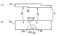
図2は本発明の第1の具体例を示すキャリア基板の図で、図2(a)は側面図、図2(b)は下面図である。これに対し、図6は従来のキャリア基板の図で、図6(a)は側面図、図6(b)は下面図である。
FIG. 2 is a view of a carrier substrate showing a first specific example of the present invention, FIG. 2 (a) is a side view, and FIG. 2 (b) is a bottom view. On the other hand, FIG. 6 is a view of a conventional carrier substrate, FIG. 6 (a) is a side view, and FIG. 6 (b) is a bottom view.
図2のキャリア基板2では、接触部21と非接触部22との段差30、即ち、境界線31が、キャリア基板2の長手方向に対して90度未満の所定の角度αをなすように形成されている。従って、接触部21と非接触部22との境界線31から非接触部22の自由端23までの、非接触部22の長手方向の長さL1が、キャリア基板2の長手方向に直交する幅方向の位置で徐々に変わるように形成されている。
In the carrier substrate 2 of FIG. 2, the step 30 between the contact portion 21 and the non-contact portion 22, that is, the boundary line 31 is formed so as to form a predetermined angle α of less than 90 degrees with respect to the longitudinal direction of the carrier substrate 2. Has been. Therefore, the length L1 in the longitudinal direction of the non-contact portion 22 from the boundary line 31 between the contact portion 21 and the non-contact portion 22 to the free end 23 of the non-contact portion 22 is a width orthogonal to the longitudinal direction of the carrier substrate 2. It is formed so as to gradually change in the direction position.
そして、このように構成することで、キャリア基板2の固有振動モードを分散させ、外部からの振動や衝撃に対して共振しにくくして、動作中の光学特性の変動を抑えている。
And by configuring in this way, the natural vibration mode of the carrier substrate 2 is dispersed to make it difficult to resonate with external vibrations and shocks, thereby suppressing fluctuations in optical characteristics during operation.
なお、境界線31は、梁の長手方向に対して、30~89度が好適である。
The boundary line 31 is preferably 30 to 89 degrees with respect to the longitudinal direction of the beam.
一方、図6に示すように、従来のキャリア基板42では、境界線50が、キャリア基板42の長手方向に対して90度の角度をなすように形成されている。そのため、キャリア基板42の固有振動モードを分散させることができなく、外部からの振動や衝撃に対して共振しやすく、動作中の光学特性が変動する。
On the other hand, as shown in FIG. 6, in the conventional carrier substrate 42, the boundary line 50 is formed so as to form an angle of 90 degrees with respect to the longitudinal direction of the carrier substrate 42. For this reason, the natural vibration mode of the carrier substrate 42 cannot be dispersed, and the carrier substrate 42 is likely to resonate with external vibration or impact, and the optical characteristics during operation vary.
図3は本発明の第2の具体例を示すキャリア基板の図で、図3(a)は側面図、図3(b)は下面図である。
FIG. 3 is a view of a carrier substrate showing a second specific example of the present invention, FIG. 3 (a) is a side view, and FIG. 3 (b) is a bottom view.
図3のキャリア基板では、境界線32が階段状をなし、接触部21と非接触部22との境界線32から非接触部22の自由端23までの、非接触部22の長手方向の長さL1が、キャリア基板2の長手方向に直交する幅方向の位置で段階的に変わるように形成されている。即ち、接触部21と非接触部22との境界線32が、複数の直線31a~31eの組み合わせからなっている。なお、複数の直線31a~31eのそれぞれの交差部分に丸みが付いていてもよい。
In the carrier substrate of FIG. 3, the boundary line 32 has a stepped shape, and the length in the longitudinal direction of the non-contact portion 22 from the boundary line 32 between the contact portion 21 and the non-contact portion 22 to the free end 23 of the non-contact portion 22. The length L1 is formed so as to change stepwise at a position in the width direction orthogonal to the longitudinal direction of the carrier substrate 2. That is, the boundary line 32 between the contact portion 21 and the non-contact portion 22 is a combination of a plurality of straight lines 31a to 31e. Note that each of the plurality of straight lines 31a to 31e may be rounded.
図4は本発明の第3の具体例を示すキャリア基板の図で、図4(a)は側面図、図4(b)は下面図である。
FIG. 4 is a view of a carrier substrate showing a third specific example of the present invention, FIG. 4 (a) is a side view, and FIG. 4 (b) is a bottom view.
図4のキャリア基板では、接触部21と非接触部22との境界線33が、キャリア基板の幅方向に対して左右対称になるように形成されている。又、境界線33の複数の直線は、キャリア基板の長手方向に対して90度未満の所定の角度βをなしている。勿論、複数の直線33a、33bの交差部分に丸みが付いていてもよい。
In the carrier substrate of FIG. 4, the boundary line 33 between the contact portion 21 and the non-contact portion 22 is formed so as to be symmetrical with respect to the width direction of the carrier substrate. The plurality of straight lines of the boundary line 33 form a predetermined angle β of less than 90 degrees with respect to the longitudinal direction of the carrier substrate. Of course, the intersection of the plurality of straight lines 33a and 33b may be rounded.
図5は本発明の第4の具体例を示すキャリア基板の図で、図5(a)は側面図、図5(b)は下面図である。
FIG. 5 is a view of a carrier substrate showing a fourth specific example of the present invention, FIG. 5 (a) is a side view, and FIG. 5 (b) is a bottom view.
図5のキャリア基板では、接触部21と非接触部22との境界線34が、円の一部、楕円の一部、2次以上の高次関数の一部、任意の曲線または複数の直線の2以上の組み合わせで形成したものである。
In the carrier substrate of FIG. 5, the boundary line 34 between the contact portion 21 and the non-contact portion 22 is a part of a circle, a part of an ellipse, a part of a higher-order function of second or higher order, an arbitrary curve, or a plurality of straight lines. These are formed by a combination of two or more.
又、接触部21と非接触部22との境界線34が、曲線になるように形成してもよい。
Further, the boundary line 34 between the contact portion 21 and the non-contact portion 22 may be formed to be a curve.
又、接触部21と非接触部22との境界線34が、一つ以上の直線と一つ以上の曲線との組み合わせでもよい。
Further, the boundary line 34 between the contact portion 21 and the non-contact portion 22 may be a combination of one or more straight lines and one or more curves.
又、この場合も、接触部21と非接触部22との境界線34が、キャリア基板2の幅方向に対して左右対称になるように形成してもよい。
Also in this case, the boundary line 34 between the contact portion 21 and the non-contact portion 22 may be formed to be bilaterally symmetric with respect to the width direction of the carrier substrate 2.
上記実施例では、キャリア基板2に段差を形成するように構成したが、キャリア基板2を面一に形成すると共に、ペルチェ素子8の上面側に段差を設けるように構成しても、上記実施例と同様な効果を得ることができる。
In the above-described embodiment, the carrier substrate 2 is configured to have a step. However, the carrier substrate 2 may be formed to be flush with the Peltier element 8 and may be configured to have a step on the upper surface side. The same effect can be obtained.
以上のように本発明について幾つかの実施例を示して説明したが、本願発明はこれらに限定されるものではなく、その技術思想を逸脱しない範囲で種々変更して実施することが可能であることは言うまでもない。
Although the present invention has been described with reference to several embodiments as described above, the present invention is not limited to these embodiments, and various modifications can be made without departing from the technical concept thereof. Needless to say.
この出願は、2008年2月12日に出願された日本出願特願2008-030740を基礎とする優先権を主張し、その開示の全てをここに取り込む。
This application claims priority based on Japanese Patent Application No. 2008-030740 filed on Feb. 12, 2008, the entire disclosure of which is incorporated herein.
Claims (12)
- 支持部材の接触部が固定部材に固定され、前記接触部と一体的に形成された非接触部が前記接触部を介して支持される支持部材の振動抑制構造であって、
前記非接触部は、振動可能な自由端を有し、
前記接触部と非接触部との境界線から前記非接触部の自由端までの、前記非接触部の長手方向の長さが、前記長手方向に直交する幅方向の位置で異なるように構成された振動抑制構造。 A support member vibration suppression structure in which a contact portion of a support member is fixed to a fixed member, and a non-contact portion formed integrally with the contact portion is supported via the contact portion,
The non-contact portion has a free end capable of vibration,
The length in the longitudinal direction of the non-contact portion from the boundary line between the contact portion and the non-contact portion to the free end of the non-contact portion is configured to be different at a position in the width direction orthogonal to the longitudinal direction. Vibration suppression structure. - 前記支持部材の接触部と非接触部との間に段差が設けられることで、前記境界線が形成される、請求の範囲第1項に記載の振動抑制構造。 The vibration suppressing structure according to claim 1, wherein the boundary line is formed by providing a step between the contact portion and the non-contact portion of the support member.
- 前記境界線が形成され、且つ前記支持部材の非接触部が、前記固定部材に接触しないように、前記固定部材に段差部が設けられている、請求の範囲第1項に記載の振動抑制構造。 The vibration suppressing structure according to claim 1, wherein the fixing member is provided with a step portion so that the boundary line is formed and the non-contact portion of the support member does not contact the fixing member. .
- 前記接触部と非接触部との境界線が、前記支持部材の長手方向に対して直交しない直線をなしている、請求の範囲第1項乃至第3項のいずれかに記載の振動抑制構造。 The vibration suppressing structure according to any one of claims 1 to 3, wherein a boundary line between the contact portion and the non-contact portion forms a straight line that is not orthogonal to the longitudinal direction of the support member.
- 前記接触部と非接触部との境界線から前記非接触部の自由端までの前記非接触部の長手方向の長さが、前記長手方向に直交する幅方向の位置で段階的に変わるように形成されている、請求の範囲第1項乃至第3項のいずれかに記載の振動抑制構造。 The length in the longitudinal direction of the non-contact portion from the boundary line between the contact portion and the non-contact portion to the free end of the non-contact portion is changed stepwise at a position in the width direction orthogonal to the longitudinal direction. The vibration suppressing structure according to any one of claims 1 to 3, wherein the vibration suppressing structure is formed.
- 前記接触部と非接触部との境界線が、複数の直線の組み合わせからなる、請求の範囲第1項乃至第5項のいずれかに記載の振動抑制構造。 The vibration suppression structure according to any one of claims 1 to 5, wherein a boundary line between the contact portion and the non-contact portion is formed of a combination of a plurality of straight lines.
- 前記接触部と非接触部との境界線が、直線と曲線との組み合わせからなる、請求の範囲第1項乃至第3項のいずれかに記載の振動抑制構造。 The vibration suppression structure according to any one of claims 1 to 3, wherein a boundary line between the contact portion and the non-contact portion is formed of a combination of a straight line and a curve.
- 前記接触部と非接触部との境界線が、曲線からなる、請求の範囲第1項乃至第3項のいずれかに記載の振動抑制構造。 The vibration suppression structure according to any one of claims 1 to 3, wherein a boundary line between the contact portion and the non-contact portion is a curved line.
- 前記接触部と非接触部との境界線が、円の一部、楕円の一部、2次以上の高次関数の一部、任意の曲線または複数の直線の2以上の組み合わせで形成されている、請求の範囲第1項乃至第3項のいずれかに記載の振動抑制構造。 A boundary line between the contact part and the non-contact part is formed by a part of a circle, a part of an ellipse, a part of a higher-order function of second order or higher, an arbitrary curve, or a combination of two or more of a plurality of straight lines. The vibration suppressing structure according to any one of claims 1 to 3, wherein:
- 前記接触部と非接触部との境界線が、前記支持部材の幅方向に対して対称になるように形成されている、請求の範囲第1項乃至第9項のいずれかに記載の振動抑制構造。 The vibration suppression according to any one of claims 1 to 9, wherein a boundary line between the contact portion and the non-contact portion is formed to be symmetric with respect to a width direction of the support member. Construction.
- 前記支持部材は、一定の長手方向の長さと一定の幅方向の長さとを有する矩形をなしている、請求の範囲第1項乃至第10項のいずれかに記載の振動抑制構造。 The vibration suppressing structure according to any one of claims 1 to 10, wherein the support member has a rectangular shape having a certain length in the longitudinal direction and a certain length in the width direction.
- 前記支持部材はキャリア基板であり、前記キャリア基板上にPLCが形成され、前記固定部材が熱制御素子である光通信用モジュールである、請求の範囲第1項乃至第11項のいずれかに記載の振動抑制構造。 12. The optical communication module according to claim 1, wherein the support member is a carrier substrate, a PLC is formed on the carrier substrate, and the fixing member is an optical communication module that is a heat control element. Vibration suppression structure.
Applications Claiming Priority (2)
| Application Number | Priority Date | Filing Date | Title |
|---|---|---|---|
| JP2008-030740 | 2008-02-12 | ||
| JP2008030740A JP5320762B2 (en) | 2008-02-12 | 2008-02-12 | Vibration suppression structure |
Publications (1)
| Publication Number | Publication Date |
|---|---|
| WO2009101902A1 true WO2009101902A1 (en) | 2009-08-20 |
Family
ID=40956934
Family Applications (1)
| Application Number | Title | Priority Date | Filing Date |
|---|---|---|---|
| PCT/JP2009/052056 WO2009101902A1 (en) | 2008-02-12 | 2009-02-06 | Structure for suppressing vibration |
Country Status (2)
| Country | Link |
|---|---|
| JP (1) | JP5320762B2 (en) |
| WO (1) | WO2009101902A1 (en) |
Families Citing this family (2)
| Publication number | Priority date | Publication date | Assignee | Title |
|---|---|---|---|---|
| JP5544793B2 (en) * | 2009-09-07 | 2014-07-09 | 富士通株式会社 | Semiconductor optical amplifier module |
| CN113726440A (en) | 2015-07-09 | 2021-11-30 | 日本电气株式会社 | Pluggable optical module and optical communication system |
Citations (10)
| Publication number | Priority date | Publication date | Assignee | Title |
|---|---|---|---|---|
| JPS6282761U (en) * | 1985-11-13 | 1987-05-27 | ||
| JPH05346130A (en) * | 1992-06-10 | 1993-12-27 | Murata Mfg Co Ltd | Vibration absorbing spring |
| JPH06283815A (en) * | 1993-03-30 | 1994-10-07 | Nippon Steel Corp | Solid state laser device |
| WO1999010882A1 (en) * | 1997-08-27 | 1999-03-04 | Nhk Spring Co., Ltd. | Objective actuator |
| JP2000131134A (en) * | 1998-10-29 | 2000-05-12 | Sumitomo Metal Ind Ltd | Resonator array, acoustic sensor and vibration sensor |
| JP2001337250A (en) * | 2000-05-25 | 2001-12-07 | Sumitomo Electric Ind Ltd | Hermetically sealed container for optical semiconductor and optical semiconductor module |
| US20030099274A1 (en) * | 2001-11-28 | 2003-05-29 | Agere Systems Optoelectronics Guardian Corp. | Laser module |
| JP2006245344A (en) * | 2005-03-03 | 2006-09-14 | Nec Corp | Wavelength-variable laser |
| JP2008028309A (en) * | 2006-07-25 | 2008-02-07 | Opnext Japan Inc | Optical transmission module |
| JP2008193003A (en) * | 2007-02-07 | 2008-08-21 | Nec Corp | Optical module |
-
2008
- 2008-02-12 JP JP2008030740A patent/JP5320762B2/en not_active Expired - Fee Related
-
2009
- 2009-02-06 WO PCT/JP2009/052056 patent/WO2009101902A1/en active Application Filing
Patent Citations (10)
| Publication number | Priority date | Publication date | Assignee | Title |
|---|---|---|---|---|
| JPS6282761U (en) * | 1985-11-13 | 1987-05-27 | ||
| JPH05346130A (en) * | 1992-06-10 | 1993-12-27 | Murata Mfg Co Ltd | Vibration absorbing spring |
| JPH06283815A (en) * | 1993-03-30 | 1994-10-07 | Nippon Steel Corp | Solid state laser device |
| WO1999010882A1 (en) * | 1997-08-27 | 1999-03-04 | Nhk Spring Co., Ltd. | Objective actuator |
| JP2000131134A (en) * | 1998-10-29 | 2000-05-12 | Sumitomo Metal Ind Ltd | Resonator array, acoustic sensor and vibration sensor |
| JP2001337250A (en) * | 2000-05-25 | 2001-12-07 | Sumitomo Electric Ind Ltd | Hermetically sealed container for optical semiconductor and optical semiconductor module |
| US20030099274A1 (en) * | 2001-11-28 | 2003-05-29 | Agere Systems Optoelectronics Guardian Corp. | Laser module |
| JP2006245344A (en) * | 2005-03-03 | 2006-09-14 | Nec Corp | Wavelength-variable laser |
| JP2008028309A (en) * | 2006-07-25 | 2008-02-07 | Opnext Japan Inc | Optical transmission module |
| JP2008193003A (en) * | 2007-02-07 | 2008-08-21 | Nec Corp | Optical module |
Also Published As
| Publication number | Publication date |
|---|---|
| JP5320762B2 (en) | 2013-10-23 |
| JP2009194025A (en) | 2009-08-27 |
Similar Documents
| Publication | Publication Date | Title |
|---|---|---|
| JP5050548B2 (en) | Optical module | |
| CN203705693U (en) | Optical module | |
| JP6872329B2 (en) | Optical fiber mounted optical integrated circuit device | |
| US20210364697A1 (en) | Optical module | |
| JP2017032629A (en) | Optical module | |
| JP2009175364A (en) | Optical module | |
| WO2009101902A1 (en) | Structure for suppressing vibration | |
| JP5834461B2 (en) | Semiconductor laser module and manufacturing method thereof | |
| JP7211236B2 (en) | optical connection structure | |
| JP4690646B2 (en) | Optical apparatus and laser module having temperature controller | |
| US11409061B2 (en) | Optical module | |
| JP2008298912A (en) | Optical element and resonance device | |
| JP5266270B2 (en) | Optical parts | |
| JP5366210B2 (en) | Optical waveguide | |
| JP2008197500A (en) | Optical module | |
| JP7028362B1 (en) | Optical module | |
| JP5458155B2 (en) | Optical receiver module | |
| CN102362401A (en) | Semiconductor laser module and suppressing member | |
| JP2010230882A (en) | Light transmission device | |
| JP4604204B2 (en) | Optical module | |
| JP2004085715A (en) | Optical module | |
| JP5182602B2 (en) | Variable dispersion compensator | |
| JP2015022018A (en) | Wavelength selection switch | |
| CN102298171A (en) | Optical waveguide device and manufacturing method of optical waveguide device | |
| JP2001066451A (en) | Optical waveguide module and its manufacture |
Legal Events
| Date | Code | Title | Description |
|---|---|---|---|
| 121 | Ep: the epo has been informed by wipo that ep was designated in this application |
Ref document number: 09710891 Country of ref document: EP Kind code of ref document: A1 |
|
| NENP | Non-entry into the national phase |
Ref country code: DE |
|
| 122 | Ep: pct application non-entry in european phase |
Ref document number: 09710891 Country of ref document: EP Kind code of ref document: A1 |