WO2009087737A1 - Radio communication device - Google Patents
Radio communication device Download PDFInfo
- Publication number
- WO2009087737A1 WO2009087737A1 PCT/JP2008/003976 JP2008003976W WO2009087737A1 WO 2009087737 A1 WO2009087737 A1 WO 2009087737A1 JP 2008003976 W JP2008003976 W JP 2008003976W WO 2009087737 A1 WO2009087737 A1 WO 2009087737A1
- Authority
- WO
- WIPO (PCT)
- Prior art keywords
- antenna
- circuit
- blocking
- frequency
- resonant frequency
- Prior art date
Links
Images


Classifications
-
- H—ELECTRICITY
- H04—ELECTRIC COMMUNICATION TECHNIQUE
- H04B—TRANSMISSION
- H04B1/00—Details of transmission systems, not covered by a single one of groups H04B3/00 - H04B13/00; Details of transmission systems not characterised by the medium used for transmission
- H04B1/02—Transmitters
- H04B1/04—Circuits
- H04B1/0475—Circuits with means for limiting noise, interference or distortion
-
- H—ELECTRICITY
- H01—ELECTRIC ELEMENTS
- H01Q—ANTENNAS, i.e. RADIO AERIALS
- H01Q1/00—Details of, or arrangements associated with, antennas
- H01Q1/12—Supports; Mounting means
- H01Q1/22—Supports; Mounting means by structural association with other equipment or articles
- H01Q1/24—Supports; Mounting means by structural association with other equipment or articles with receiving set
- H01Q1/241—Supports; Mounting means by structural association with other equipment or articles with receiving set used in mobile communications, e.g. GSM
- H01Q1/242—Supports; Mounting means by structural association with other equipment or articles with receiving set used in mobile communications, e.g. GSM specially adapted for hand-held use
- H01Q1/243—Supports; Mounting means by structural association with other equipment or articles with receiving set used in mobile communications, e.g. GSM specially adapted for hand-held use with built-in antennas
-
- H—ELECTRICITY
- H01—ELECTRIC ELEMENTS
- H01Q—ANTENNAS, i.e. RADIO AERIALS
- H01Q21/00—Antenna arrays or systems
- H01Q21/28—Combinations of substantially independent non-interacting antenna units or systems
-
- H—ELECTRICITY
- H01—ELECTRIC ELEMENTS
- H01Q—ANTENNAS, i.e. RADIO AERIALS
- H01Q5/00—Arrangements for simultaneous operation of antennas on two or more different wavebands, e.g. dual-band or multi-band arrangements
- H01Q5/30—Arrangements for providing operation on different wavebands
- H01Q5/307—Individual or coupled radiating elements, each element being fed in an unspecified way
- H01Q5/342—Individual or coupled radiating elements, each element being fed in an unspecified way for different propagation modes
- H01Q5/357—Individual or coupled radiating elements, each element being fed in an unspecified way for different propagation modes using a single feed point
- H01Q5/364—Creating multiple current paths
-
- H—ELECTRICITY
- H03—ELECTRONIC CIRCUITRY
- H03F—AMPLIFIERS
- H03F1/00—Details of amplifiers with only discharge tubes, only semiconductor devices or only unspecified devices as amplifying elements
- H03F1/02—Modifications of amplifiers to raise the efficiency, e.g. gliding Class A stages, use of an auxiliary oscillation
-
- H—ELECTRICITY
- H03—ELECTRONIC CIRCUITRY
- H03F—AMPLIFIERS
- H03F3/00—Amplifiers with only discharge tubes or only semiconductor devices as amplifying elements
- H03F3/20—Power amplifiers, e.g. Class B amplifiers, Class C amplifiers
- H03F3/24—Power amplifiers, e.g. Class B amplifiers, Class C amplifiers of transmitter output stages
-
- H—ELECTRICITY
- H04—ELECTRIC COMMUNICATION TECHNIQUE
- H04B—TRANSMISSION
- H04B1/00—Details of transmission systems, not covered by a single one of groups H04B3/00 - H04B13/00; Details of transmission systems not characterised by the medium used for transmission
- H04B1/02—Transmitters
- H04B1/04—Circuits
- H04B2001/0408—Circuits with power amplifiers
- H04B2001/045—Circuits with power amplifiers with means for improving efficiency
-
- H—ELECTRICITY
- H04—ELECTRIC COMMUNICATION TECHNIQUE
- H04M—TELEPHONIC COMMUNICATION
- H04M1/00—Substation equipment, e.g. for use by subscribers
- H04M1/02—Constructional features of telephone sets
- H04M1/0202—Portable telephone sets, e.g. cordless phones, mobile phones or bar type handsets
- H04M1/0206—Portable telephones comprising a plurality of mechanically joined movable body parts, e.g. hinged housings
- H04M1/0208—Portable telephones comprising a plurality of mechanically joined movable body parts, e.g. hinged housings characterized by the relative motions of the body parts
- H04M1/0214—Foldable telephones, i.e. with body parts pivoting to an open position around an axis parallel to the plane they define in closed position
Definitions
- the switch 17 switches between the case where the matching circuit 16 and the termination circuit 18 are connected and the case where the matching circuit 16 and the wireless unit 19 are connected under the control of the control unit 10.
- the wireless unit 63 wirelessly processes the signal input from the matching circuit 62.
- the wireless unit 66 wirelessly processes the signal input from the matching circuit 65.
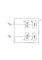
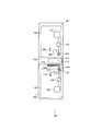
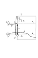
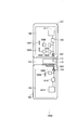
- the first housing 101 has a circuit board 106 inside.
- the hinge portion 103 has a hinge conductive portion 113.
- the circuit board 106 is provided with the power supply unit 107, and is provided with the cutoff circuit 108, the termination circuit 109, the matching circuit 110, and the wireless unit 111.
- the circuit board 106 has a stacked structure.
- one layer forming the laminated structure of the circuit board 106 is a ground layer (not shown), and the ground layer is formed by printing over substantially the entire surface of the circuit board 106.
- the blocking circuit 108, the termination circuit 109, the matching circuit 110, and the wireless unit 111 will be described later.
- the hinge conductive portion 113 is formed of a conductive member, and functions as a rotating shaft when the hinge portion 103 rotates.
- the feeding unit 114 feeds power to the antenna 115.
- the antenna 115 is, for example, an antenna for cellular communication, and is fed from the feeding unit 114.
- the antenna 115 is composed of a long piece portion 115a and a short piece portion 115b extending from one end of the long piece portion 115a in a direction perpendicular to the longitudinal direction of the long piece portion 115a. It has become.
- the antenna 115 is fed by the feeding portion 114 from the tip end of the short piece portion 115 b.
- the circuit board 116 is provided with the power supply unit 114, and is provided with the blocking circuit 117, the termination circuit 118, the matching circuit 119, and the wireless unit 120.
- the circuit board 116 has a laminated structure.
- one layer forming the laminated structure of the circuit board 116 is a ground layer (not shown), and the ground layer is formed by printing over substantially the entire surface of the circuit board 116.
- the blocking circuit 117, the termination circuit 118, the matching circuit 119, and the radio unit 120 will be described later.
- a display unit (not shown) is provided in the first housing 101, and an operation unit (not shown) such as a key switch operated in a call etc. is provided in the second housing 102.
- the power feeding unit 107 feeds power to the ground layer of the circuit board 106 and the hinge conductive unit 113. Further, in the wireless communication device 100, since the long piece portion 115a of the antenna 115 is disposed close to the hinge conductive portion 113, the long piece portion 115a of the antenna 115 and the hinge conductive portion 113 are electrically coupled by electrostatic capacitive coupling. As a result, the hinge conductive portion 113 and the antenna 115 are electrically connected by capacitive coupling. Thus, the wireless communication device 100 configures an antenna by the ground layer of the circuit board 106, the hinge conductive unit 113, the antenna 115, and the ground layer of the circuit board 116.
- the antenna formed by the ground layer of the circuit board 106, the hinge conductive portion 113, the antenna 115, and the ground layer of the circuit board 116 and the antenna 115 are disposed close to each other, whereby the ground layer of the circuit board 106, hinge conductive
- the antenna composed of the portion 113, the antenna 115 and the ground layer of the circuit board 116, and the antenna 115 are affected by each other's amplitude.
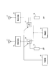
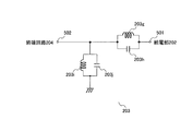
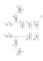
- the matching circuit 205 and the wireless unit 206 constitute signal processing means for processing a signal received by the antenna 201. Further, the matching circuit 211 and the wireless unit 212 constitute a signal processing unit that processes a signal received by the antenna 207.
- the antenna 201 corresponds to the antenna 115 of FIG. 3 and is, for example, an antenna for cellular communication, and the resonance frequency at that time is in the 2 GHz band.
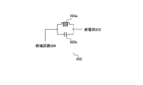
- the feeding unit 202 corresponds to the feeding unit 114 in FIG. 3 and feeds power to the antenna 201 and is electrically connected to the blocking circuit 203 and the matching circuit 205.
- the feed unit 202 indicates the boundary between the wireless unit and the antenna.
- the blocking circuit 203 corresponds to the blocking circuit 117 in FIG. 3 and is connected to the antenna 201 in parallel with the matching circuit 205, and blocks the resonant frequency of the antenna 201.
- the blocking circuit 203 is, for example, an LC parallel resonant circuit, a low pass filter, a high pass filter, or a band pass filter.
- the blocking circuit 203 also blocks, for example, a frequency of 2 GHz band that is a resonant frequency of the antenna 201.
- the detailed configuration of the shutoff circuit 203 will be described later.
- the antenna 207 corresponds to an antenna configured by the ground layer of the circuit board 106 of FIG. 3, the hinge conductive portion 113, the antenna 115, and the ground layer of the circuit board 116.
- the antenna 207 is disposed close to the antenna 201 and is, for example, an antenna for one segment broadcasting of terrestrial digital broadcasting, and the resonance frequency at that time is a 500 MHz band.
- the blocking circuit 209 corresponds to the blocking circuit 108 in FIG. 3 and is connected to the antenna 207 in parallel with the matching circuit 211, and blocks the resonant frequency of the antenna 207.
- the blocking circuit 209 is, for example, an LC parallel resonant circuit, a low pass filter, a high pass filter, or a band pass filter.
- the blocking circuit 209 also blocks, for example, the frequency of the 500 MHz band, which is the resonant frequency of the antenna 207. The detailed configuration of blocking circuit 209 will be described later.
- the blocking circuit 203 is an LC parallel resonant circuit in which the reactance 203a and the capacitor 203b are connected in parallel, and a circuit configuration in which the LC parallel resonant circuit is connected in series between the antenna 201 and the termination circuit 204 is Have. Then, the blocking circuit 203 blocks the resonant frequency of the antenna 201 by this LC parallel resonant circuit, and passes the other frequencies. For example, the blocking circuit 203 blocks frequencies in the 2 GHz band and passes frequencies other than the 2 GHz band.
- the blocking circuit 209 can also be configured the same as the LC parallel resonant circuit of FIG. 5. In this case, the blocking circuit 209 cuts off the resonant frequency of the antenna 207 by this LC parallel resonant circuit, and passes other frequencies. For example, the blocking circuit 209 blocks the frequency of the 500 MHz band and passes frequencies other than the 500 MHz band.
- the blocking circuit 209 can also be configured the same as the band pass filter circuit of FIG. In this case, the cutoff circuit 209 cuts off the resonant frequency of the antenna 207 by this band pass filter circuit, and passes the other frequencies. For example, the blocking circuit 209 passes a frequency of 2 GHz, which is the resonant frequency of the antenna 201, and blocks frequencies other than 2 GHz.
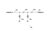
- the termination circuit 210 has a circuit configuration in which a capacitor 210a is connected in series between the blocking circuit 209 and the ground.
- FIG. 11 is a diagram showing an equivalent circuit in the processing sequence of the antenna 207.
- the processing sequence of the antenna 207 is a sequence including the antenna 207, the power feeding unit 208, the blocking circuit 209, the termination circuit 210, the matching circuit 211, and the wireless unit 212.
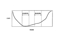
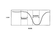
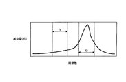
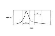
- VSWR is voltage standing wave ratio (Voltage Standing Wave Ratio).
- Voltage Standing Wave Ratio Voltage Standing Wave Ratio
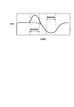
- a standing wave is generated by interference between a traveling wave transmitted from a transmitter to an antenna and a reflected wave.
- VSWR is an index to evaluate antenna performance.
- the current supplied from the feeding unit 202 is attenuated while moving away from the feeding unit 202 and flows through the ground layer of the circuit board, so the amount of current from the feeding unit 202 becomes larger as it is closer to the feeding unit 202. Therefore, as the antenna 207 is closer to the feeding unit 202, the influence from the feeding unit 202 becomes larger. Under such circumstances, the termination unit 210 controls the phase of the current by changing the electrical length of the antenna 207, and makes the amplitude of the antenna 207 different from the amplitude of the antenna 201, thereby preventing deterioration of the antenna characteristics. .
- the electrical length is the distance represented by the wavelength in the medium at a certain frequency.
- the phase indicates in which position of a period a specific place is in a waveform whose period is the electrical length of the wavelength ⁇ at a certain frequency.
- the electrical length and the phase can be expressed by the following equations (1) and (2).
- the antenna 1801 is, for example, an antenna for cellular communication, and is fed from the feeding unit 114. Also, the antenna 1801 has two different resonant frequencies. The details of the configuration of the antenna 1801 will be described later.
- the antenna 1801 also functions as an antenna configured by the ground layer of the circuit board 106, the hinge conductive portion 113, the antenna 1801, and the ground layer of the circuit board 116. Therefore, the antenna formed by the ground layer of the circuit board 106, the hinge conductive portion 113, the antenna 1801, and the ground layer of the circuit board 116 and the antenna 1801 are disposed close to each other, The antenna performance is degraded because the current flows to the other antenna by operation.
- An antenna 2001 corresponds to the antenna 1801 in FIG. 20, and is disposed close to the antenna 207.
- the antenna 2001 is, for example, an antenna for cellular communication, and has two resonant frequencies.
- the antenna 2001 has, for example, resonant frequencies of 800 MHz and 2 GHz.
- the blocking circuit 2011 corresponds to the blocking circuit 1806 in FIG. 20, is connected in series between the blocking circuit 2010 and the termination circuit 2012, and blocks the resonant frequency of the antenna 207.
- the blocking circuit 2011 is, for example, an LC parallel resonant circuit, a low pass filter, a high pass filter, or a band pass filter. Further, the blocking circuit 2011 blocks, for example, a frequency of 470 MHz to 770 MHz, which is a resonant frequency of the antenna 207.
- the configuration of the blocking circuit 2011 is the same as any one of FIGS. 5 to 8, and thus the description thereof is omitted.
- an antenna having two resonance frequencies and an antenna having one resonance frequency are close to each other. Also in this case, deterioration of the antenna characteristics can be prevented.
- the feeding unit 208 feeds power to the antenna 207 and is electrically connected to the blocking circuit 209 and the blocking circuit 2201.
- the blocking circuit 2201 is connected in series between the feeding unit 208 and the matching circuit 211, and blocks the resonant frequency of the antenna 201. In addition, the blocking circuit 2201 increases the VSWR at the resonant frequency of the antenna 201 by increasing the amount of attenuation at the resonant frequency of the antenna 201.
- the blocking circuit 2201 is, for example, an LC parallel resonant circuit.
- proximity is achieved by connecting in series between the antenna and the matching circuit a blocking circuit that blocks the resonant frequency of the adjacent antenna.
- the performance of the antenna can be further improved.
- the blocking circuit and the termination circuit are connected in parallel with the matching circuit to the two antennas in close proximity to each other, but the present invention is not limited to this.
- a blocking circuit and a termination circuit may be connected in parallel with the matching circuit with respect to only one of the two adjacent antennas.
- the wireless communication apparatus is suitable for performing communication using a plurality of closely spaced antennas having different resonance frequencies.
Abstract
Description
図3は、本発明の実施の形態1に係る開いた状態の無線通信装置100の内部の平面図である。 Embodiment 1
FIG. 3 is a plan view of the inside of the
Lは、機械長(実測長)位相p[度]=(L/λ)×1×π (2)ただし、Lは、機械長(実測長)
λは、波長
上記より、(2)式を(1)式に代入することにより、位相pは電気長Leによって一意に決まることがわかる。また、波長λである周波数における位相pは、機械長Lと媒質の特性である速度係数によって決まる。 Here, in the radio wave propagation, the electrical length is the distance represented by the wavelength in the medium at a certain frequency. Further, the phase indicates in which position of a period a specific place is in a waveform whose period is the electrical length of the wavelength λ at a certain frequency. Further, the electrical length and the phase can be expressed by the following equations (1) and (2). Electric length Le [m] = Ve × L (1) where Ve is the velocity coefficient (ratio of electromagnetic wave transmission velocity in vacuum and in medium)
L is the machine length (measured length) phase p [degree] = (L / λ) × 1 × π (2) where L is the machine length (measured length)
From the wavelength described above, it is understood that the phase p is uniquely determined by the electric length Le by substituting the equation (2) into the equation (1). Further, the phase p at the frequency of wavelength λ is determined by the machine length L and the speed coefficient which is the characteristic of the medium.
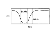
従って、終端部210は、(3)式を用いてアンテナ207の位相Mを制御することにより、アンテナ201の振幅が最大となる場所とアンテナ207の振幅が最小となる場所とが、距離的に近接する位相になるように制御する。因みに、アンテナ207の振幅が最小になるのは、給電部202からの電気長Meがλ/4、(3×λ)/4、(5×λ)/4、(7×λ)/4、・・・、(λ×(2n+1))/4の場合である。 Specifically, the wavelength of the radio wave received by the
Therefore, by controlling the phase M of the
図20は、本発明の実施の形態2に係る開いた状態の無線通信装置1800の内部の平面図である。 Second Embodiment
FIG. 20 is a plan view of the inside of the
図24は、本発明の実施の形態3に係る無線通信装置2200の構成を示すブロック図である。 Third Embodiment
FIG. 24 is a block diagram showing a configuration of
Claims (5)
- 第1アンテナと、
前記第1アンテナに近接して配置される第2アンテナと、
前記第1アンテナで受信した信号を処理する第1信号処理手段と、
前記第1信号処理手段と並列に前記第1アンテナに接続されるとともに、前記第1アンテナの共振周波数を遮断する第1遮断手段と、
前記第1遮断手段の出力側を電気的に終端する第1終端手段と、
前記第1アンテナの共振周波数とは異なる共振周波数を有する前記第2アンテナで受信した信号を処理する第2信号処理手段と、
を具備する無線通信装置。 A first antenna,
A second antenna disposed proximate to the first antenna;
First signal processing means for processing a signal received by the first antenna;
First blocking means connected in parallel to the first signal processing means to the first antenna and blocking the resonant frequency of the first antenna;
First termination means for electrically terminating the output side of the first blocking means;
Second signal processing means for processing a signal received by the second antenna having a resonant frequency different from the resonant frequency of the first antenna;
A wireless communication device comprising - 前記第2信号処理手段と並列に前記第2アンテナに接続されるとともに、前記第2アンテナの共振周波数を遮断する第2遮断手段と、
前記第2遮断手段の出力側を電気的に終端する第2終端手段と、
を具備する請求項1記載の無線通信装置。 Second blocking means connected in parallel to the second signal processing means to the second antenna and blocking the resonant frequency of the second antenna;
Second termination means for electrically terminating the output side of the second blocking means;
The wireless communication device according to claim 1, comprising: - 前記第1アンテナと前記第1信号処理手段の間に直列に接続されるとともに、前記第2アンテナの共振周波数を遮断する第3遮断手段を具備する請求項1記載の無線通信装置。 The wireless communication apparatus according to claim 1, further comprising third blocking means connected in series between the first antenna and the first signal processing means and blocking the resonant frequency of the second antenna.
- 前記第2信号処理手段と並列に前記第2アンテナに接続されるとともに、前記第1アンテナの第1共振周波数を遮断する第2遮断手段と、
前記第2遮断手段の出力側に接続される前記第2アンテナの共振周波数を遮断する第3遮断手段と、
前記第3遮断手段の出力側を終端する第2終端手段と、
前記第2信号処理手段及び前記第2遮断手段と並列に接続されるとともに、前記第1共振周波数と異なる周波数である前記第1アンテナの第2共振周波数を遮断する第4遮断手段と、
前記第4遮断手段の出力側に接続される前記第2アンテナの共振周波数を遮断する第5遮断手段と、
前記第5遮断手段の出力側を終端する第3終端手段と、
を具備する請求項1記載の無線通信装置。 A second blocking means connected to the second antenna in parallel with the second signal processing means and blocking the first resonant frequency of the first antenna;
Third blocking means for blocking the resonant frequency of the second antenna connected to the output side of the second blocking means;
Second termination means for terminating the output side of the third blocking means;
Fourth blocking means connected in parallel with the second signal processing means and the second blocking means and blocking the second resonant frequency of the first antenna that is a frequency different from the first resonant frequency;
Fifth blocking means for blocking the resonant frequency of the second antenna connected to the output side of the fourth blocking means;
Third termination means for terminating the output side of the fifth blocking means;
The wireless communication device according to claim 1, comprising: - 前記第1アンテナと前記第2アンテナの何れか一方がセルラー通信用のアンテナである請求項1記載の無線通信装置。 The wireless communication apparatus according to claim 1, wherein one of the first antenna and the second antenna is an antenna for cellular communication.
Priority Applications (2)
| Application Number | Priority Date | Filing Date | Title |
|---|---|---|---|
| BRPI0822152-9A BRPI0822152A2 (en) | 2008-01-10 | 2008-12-25 | Radio communication device |
| US12/812,451 US20100285836A1 (en) | 2008-01-10 | 2008-12-25 | Radio communication device |
Applications Claiming Priority (2)
| Application Number | Priority Date | Filing Date | Title |
|---|---|---|---|
| JP2008-003186 | 2008-01-10 | ||
| JP2008003186A JP4358886B2 (en) | 2008-01-10 | 2008-01-10 | Wireless communication device |
Publications (1)
| Publication Number | Publication Date |
|---|---|
| WO2009087737A1 true WO2009087737A1 (en) | 2009-07-16 |
Family
ID=40852862
Family Applications (1)
| Application Number | Title | Priority Date | Filing Date |
|---|---|---|---|
| PCT/JP2008/003976 WO2009087737A1 (en) | 2008-01-10 | 2008-12-25 | Radio communication device |
Country Status (4)
| Country | Link |
|---|---|
| US (1) | US20100285836A1 (en) |
| JP (1) | JP4358886B2 (en) |
| BR (1) | BRPI0822152A2 (en) |
| WO (1) | WO2009087737A1 (en) |
Families Citing this family (35)
| Publication number | Priority date | Publication date | Assignee | Title |
|---|---|---|---|---|
| US8744384B2 (en) | 2000-07-20 | 2014-06-03 | Blackberry Limited | Tunable microwave devices with auto-adjusting matching circuit |
| US9406444B2 (en) | 2005-11-14 | 2016-08-02 | Blackberry Limited | Thin film capacitors |
| US7711337B2 (en) | 2006-01-14 | 2010-05-04 | Paratek Microwave, Inc. | Adaptive impedance matching module (AIMM) control architectures |
| US7535312B2 (en) | 2006-11-08 | 2009-05-19 | Paratek Microwave, Inc. | Adaptive impedance matching apparatus, system and method with improved dynamic range |
| US7714676B2 (en) | 2006-11-08 | 2010-05-11 | Paratek Microwave, Inc. | Adaptive impedance matching apparatus, system and method |
| US7917104B2 (en) | 2007-04-23 | 2011-03-29 | Paratek Microwave, Inc. | Techniques for improved adaptive impedance matching |
| US8213886B2 (en) | 2007-05-07 | 2012-07-03 | Paratek Microwave, Inc. | Hybrid techniques for antenna retuning utilizing transmit and receive power information |
| US7991363B2 (en) | 2007-11-14 | 2011-08-02 | Paratek Microwave, Inc. | Tuning matching circuits for transmitter and receiver bands as a function of transmitter metrics |
| US8072285B2 (en) | 2008-09-24 | 2011-12-06 | Paratek Microwave, Inc. | Methods for tuning an adaptive impedance matching network with a look-up table |
| US8472888B2 (en) | 2009-08-25 | 2013-06-25 | Research In Motion Rf, Inc. | Method and apparatus for calibrating a communication device |
| US9026062B2 (en) | 2009-10-10 | 2015-05-05 | Blackberry Limited | Method and apparatus for managing operations of a communication device |
| KR101839425B1 (en) * | 2009-12-07 | 2018-03-16 | 삼성전자 주식회사 | A portable terminal and method for operating antenna thereof |
| US8803631B2 (en) | 2010-03-22 | 2014-08-12 | Blackberry Limited | Method and apparatus for adapting a variable impedance network |
| AU2011242798B2 (en) | 2010-04-20 | 2015-01-15 | Blackberry Limited | Method and apparatus for managing interference in a communication device |
| CN103155423B (en) * | 2010-10-25 | 2014-11-12 | 夏普株式会社 | Wireless communication device and method for controlling wireless communication device |
| US9379454B2 (en) | 2010-11-08 | 2016-06-28 | Blackberry Limited | Method and apparatus for tuning antennas in a communication device |
| US8712340B2 (en) | 2011-02-18 | 2014-04-29 | Blackberry Limited | Method and apparatus for radio antenna frequency tuning |
| US8655286B2 (en) | 2011-02-25 | 2014-02-18 | Blackberry Limited | Method and apparatus for tuning a communication device |
| US8594584B2 (en) | 2011-05-16 | 2013-11-26 | Blackberry Limited | Method and apparatus for tuning a communication device |
| US8626083B2 (en) | 2011-05-16 | 2014-01-07 | Blackberry Limited | Method and apparatus for tuning a communication device |
| EP2740221B1 (en) | 2011-08-05 | 2019-06-26 | BlackBerry Limited | Method and apparatus for band tuning in a communication device |
| US9673867B2 (en) * | 2012-03-14 | 2017-06-06 | Semiconductor Energy Laboratory Co., Ltd. | Power transmission device and power feeding system |
| US8948889B2 (en) | 2012-06-01 | 2015-02-03 | Blackberry Limited | Methods and apparatus for tuning circuit components of a communication device |
| US9853363B2 (en) | 2012-07-06 | 2017-12-26 | Blackberry Limited | Methods and apparatus to control mutual coupling between antennas |
| US9246223B2 (en) | 2012-07-17 | 2016-01-26 | Blackberry Limited | Antenna tuning for multiband operation |
| US9413066B2 (en) | 2012-07-19 | 2016-08-09 | Blackberry Limited | Method and apparatus for beam forming and antenna tuning in a communication device |
| US9350405B2 (en) | 2012-07-19 | 2016-05-24 | Blackberry Limited | Method and apparatus for antenna tuning and power consumption management in a communication device |
| US9362891B2 (en) | 2012-07-26 | 2016-06-07 | Blackberry Limited | Methods and apparatus for tuning a communication device |
| US10404295B2 (en) | 2012-12-21 | 2019-09-03 | Blackberry Limited | Method and apparatus for adjusting the timing of radio antenna tuning |
| US9374113B2 (en) | 2012-12-21 | 2016-06-21 | Blackberry Limited | Method and apparatus for adjusting the timing of radio antenna tuning |
| US9438319B2 (en) | 2014-12-16 | 2016-09-06 | Blackberry Limited | Method and apparatus for antenna selection |
| JP6666067B2 (en) * | 2014-12-25 | 2020-03-13 | 京セラ株式会社 | Mobile terminal |
| TW201630510A (en) * | 2015-02-09 | 2016-08-16 | 鴻海精密工業股份有限公司 | Protect case |
| WO2017091993A1 (en) * | 2015-12-03 | 2017-06-08 | 华为技术有限公司 | Multi-frequency communication antenna and base station |
| CN106450776B (en) * | 2016-09-29 | 2019-06-11 | 宇龙计算机通信科技(深圳)有限公司 | Antenna assembly and mobile terminal |
Citations (5)
| Publication number | Priority date | Publication date | Assignee | Title |
|---|---|---|---|---|
| JPH07202774A (en) * | 1993-12-28 | 1995-08-04 | Toshiba Corp | Radio equipment |
| JP2004096303A (en) * | 2002-08-30 | 2004-03-25 | Kyocera Corp | Control method for gain of antenna structure, antenna structure, and communication apparatus |
| JP2004274445A (en) * | 2003-03-10 | 2004-09-30 | Sony Ericsson Mobilecommunications Japan Inc | Antenna device and radio equipment |
| JP2006042255A (en) * | 2004-07-30 | 2006-02-09 | Matsushita Electric Ind Co Ltd | Wireless communication device |
| JP2007174034A (en) * | 2005-12-20 | 2007-07-05 | Matsushita Electric Ind Co Ltd | Receiver, and electronic equipment using same |
Family Cites Families (6)
| Publication number | Priority date | Publication date | Assignee | Title |
|---|---|---|---|---|
| US4388496A (en) * | 1980-08-11 | 1983-06-14 | Trio Kabushiki Kaisha | FM/AM Stereo receiver |
| DE19704151C1 (en) * | 1997-02-04 | 1998-08-27 | Siemens Ag | Transmit-receive switching arrangement |
| JP3551899B2 (en) * | 2000-06-26 | 2004-08-11 | 株式会社村田製作所 | Resonator, filter, duplexer and communication device |
| TW595131B (en) * | 2003-03-26 | 2004-06-21 | Winbond Electronics Corp | Wireless transmission system and its wireless receiving device |
| US7505790B2 (en) * | 2005-06-07 | 2009-03-17 | Integrated Systems Solution Corp. | Antenna diversity switch of wireless dual-mode co-existence systems |
| JP4643624B2 (en) * | 2007-09-21 | 2011-03-02 | 株式会社東芝 | ANTENNA DEVICE AND ELECTRONIC DEVICE |
-
2008
- 2008-01-10 JP JP2008003186A patent/JP4358886B2/en not_active Expired - Fee Related
- 2008-12-25 US US12/812,451 patent/US20100285836A1/en not_active Abandoned
- 2008-12-25 BR BRPI0822152-9A patent/BRPI0822152A2/en not_active IP Right Cessation
- 2008-12-25 WO PCT/JP2008/003976 patent/WO2009087737A1/en active Application Filing
Patent Citations (5)
| Publication number | Priority date | Publication date | Assignee | Title |
|---|---|---|---|---|
| JPH07202774A (en) * | 1993-12-28 | 1995-08-04 | Toshiba Corp | Radio equipment |
| JP2004096303A (en) * | 2002-08-30 | 2004-03-25 | Kyocera Corp | Control method for gain of antenna structure, antenna structure, and communication apparatus |
| JP2004274445A (en) * | 2003-03-10 | 2004-09-30 | Sony Ericsson Mobilecommunications Japan Inc | Antenna device and radio equipment |
| JP2006042255A (en) * | 2004-07-30 | 2006-02-09 | Matsushita Electric Ind Co Ltd | Wireless communication device |
| JP2007174034A (en) * | 2005-12-20 | 2007-07-05 | Matsushita Electric Ind Co Ltd | Receiver, and electronic equipment using same |
Also Published As
| Publication number | Publication date |
|---|---|
| JP2009165083A (en) | 2009-07-23 |
| US20100285836A1 (en) | 2010-11-11 |
| JP4358886B2 (en) | 2009-11-04 |
| BRPI0822152A2 (en) | 2015-06-23 |
Similar Documents
| Publication | Publication Date | Title |
|---|---|---|
| WO2009087737A1 (en) | Radio communication device | |
| KR100783634B1 (en) | An antenna device and method for transmitting and/or receiving rf waves, and radio communication device comprising the same | |
| JP5412871B2 (en) | Antenna, radiation pattern switching method thereof, and wireless communication apparatus | |
| FI113911B (en) | Method for coupling a signal and antenna structure | |
| EP2950387B1 (en) | Antennas with multiple feed circuits | |
| WO2006062060A1 (en) | Radio antenna device and mobile radio device using the same | |
| EP1484817A1 (en) | Antenna | |
| US10601114B2 (en) | Multi-part radio apparatus | |
| US20080266199A1 (en) | Adjustable antenna and methods | |
| CN1954460A (en) | Multi-band antenna systems including a plurality of separate low-band frequency antennas, wireless terminals and radiotelephones incorporating the same | |
| WO2004049583A1 (en) | Radio communication apparatus | |
| EP1055266A1 (en) | Dual band diversity antenna having parasitic radiating element | |
| WO2006090673A1 (en) | Portable wireless device | |
| US8207898B2 (en) | Antenna unit and communication apparatus | |
| JP4704287B2 (en) | Antenna device and portable radio | |
| KR101448258B1 (en) | Internal antenna capable of frequency tuning | |
| EP1470612A2 (en) | Multi-band sleeve dipole antenna | |
| US20120098712A1 (en) | Portable wireless terminal | |
| JP4441582B2 (en) | Wireless communication device | |
| CN104767026A (en) | Seven-frequency-band covering small mobile communication device antenna | |
| US8847827B2 (en) | Communication apparatus | |
| JP2006042255A (en) | Wireless communication device | |
| JP2008136189A (en) | Foldable mobile wireless apparatus | |
| KR101776261B1 (en) | Metamaterial antenna | |
| JP2010252057A (en) | Mobile wireless device |
Legal Events
| Date | Code | Title | Description |
|---|---|---|---|
| 121 | Ep: the epo has been informed by wipo that ep was designated in this application |
Ref document number: 08870272 Country of ref document: EP Kind code of ref document: A1 |
|
| WWE | Wipo information: entry into national phase |
Ref document number: 12812451 Country of ref document: US |
|
| NENP | Non-entry into the national phase |
Ref country code: DE |
|
| 122 | Ep: pct application non-entry in european phase |
Ref document number: 08870272 Country of ref document: EP Kind code of ref document: A1 |
|
| ENP | Entry into the national phase |
Ref document number: PI0822152 Country of ref document: BR Kind code of ref document: A2 Effective date: 20100712 |