WO2009018581A1 - Copper metallization of through silicon via - Google Patents
Copper metallization of through silicon via Download PDFInfo
- Publication number
- WO2009018581A1 WO2009018581A1 PCT/US2008/072136 US2008072136W WO2009018581A1 WO 2009018581 A1 WO2009018581 A1 WO 2009018581A1 US 2008072136 W US2008072136 W US 2008072136W WO 2009018581 A1 WO2009018581 A1 WO 2009018581A1
- Authority
- WO
- WIPO (PCT)
- Prior art keywords
- copper
- microns
- concentration
- feature
- acid
- Prior art date
Links
- 239000010949 copper Substances 0.000 title claims abstract description 199
- RYGMFSIKBFXOCR-UHFFFAOYSA-N Copper Chemical compound [Cu] RYGMFSIKBFXOCR-UHFFFAOYSA-N 0.000 title claims abstract description 188
- 229910052802 copper Inorganic materials 0.000 title claims abstract description 188
- 229910052710 silicon Inorganic materials 0.000 title claims abstract description 38
- 239000010703 silicon Substances 0.000 title claims abstract description 38
- 238000001465 metallisation Methods 0.000 title description 31
- 230000008021 deposition Effects 0.000 claims abstract description 106
- 239000000203 mixture Substances 0.000 claims abstract description 74
- 238000000034 method Methods 0.000 claims abstract description 51
- JPVYNHNXODAKFH-UHFFFAOYSA-N Cu2+ Chemical compound [Cu+2] JPVYNHNXODAKFH-UHFFFAOYSA-N 0.000 claims abstract description 41
- 229910001431 copper ion Inorganic materials 0.000 claims abstract description 40
- 239000000758 substrate Substances 0.000 claims abstract description 36
- VEXZGXHMUGYJMC-UHFFFAOYSA-M Chloride anion Chemical compound [Cl-] VEXZGXHMUGYJMC-UHFFFAOYSA-M 0.000 claims abstract description 18
- 239000004065 semiconductor Substances 0.000 claims abstract description 16
- 150000002894 organic compounds Chemical class 0.000 claims abstract description 8
- LSNNMFCWUKXFEE-UHFFFAOYSA-M Bisulfite Chemical compound OS([O-])=O LSNNMFCWUKXFEE-UHFFFAOYSA-M 0.000 claims abstract description 4
- 150000007522 mineralic acids Chemical class 0.000 claims abstract 2
- AFVFQIVMOAPDHO-UHFFFAOYSA-N Methanesulfonic acid Chemical compound CS(O)(=O)=O AFVFQIVMOAPDHO-UHFFFAOYSA-N 0.000 claims description 36
- -1 poly(propylene glycol) Polymers 0.000 claims description 29
- 239000002253 acid Substances 0.000 claims description 27
- 150000001875 compounds Chemical class 0.000 claims description 27
- 238000011049 filling Methods 0.000 claims description 25
- BSXVKCJAIJZTAV-UHFFFAOYSA-L copper;methanesulfonate Chemical compound [Cu+2].CS([O-])(=O)=O.CS([O-])(=O)=O BSXVKCJAIJZTAV-UHFFFAOYSA-L 0.000 claims description 21
- KGIGUEBEKRSTEW-UHFFFAOYSA-N 2-vinylpyridine Chemical group C=CC1=CC=CC=N1 KGIGUEBEKRSTEW-UHFFFAOYSA-N 0.000 claims description 18
- 229920000642 polymer Polymers 0.000 claims description 16
- 125000002496 methyl group Chemical group [H]C([H])([H])* 0.000 claims description 15
- 229910052751 metal Inorganic materials 0.000 claims description 14
- 239000002184 metal Substances 0.000 claims description 14
- 229940098779 methanesulfonic acid Drugs 0.000 claims description 14
- 150000002898 organic sulfur compounds Chemical group 0.000 claims description 10
- LMPMFQXUJXPWSL-UHFFFAOYSA-N 3-(3-sulfopropyldisulfanyl)propane-1-sulfonic acid Chemical group OS(=O)(=O)CCCSSCCCS(O)(=O)=O LMPMFQXUJXPWSL-UHFFFAOYSA-N 0.000 claims description 8
- 125000004432 carbon atom Chemical group C* 0.000 claims description 7
- 125000004076 pyridyl group Chemical group 0.000 claims description 7
- 229920001451 polypropylene glycol Polymers 0.000 claims description 6
- 229920001577 copolymer Polymers 0.000 claims description 5
- QGZKDVFQNNGYKY-UHFFFAOYSA-O Ammonium Chemical group [NH4+] QGZKDVFQNNGYKY-UHFFFAOYSA-O 0.000 claims description 4
- 125000002947 alkylene group Chemical group 0.000 claims description 4
- 125000004122 cyclic group Chemical group 0.000 claims description 4
- 239000001257 hydrogen Substances 0.000 claims description 4
- 229910052739 hydrogen Inorganic materials 0.000 claims description 4
- 125000004435 hydrogen atom Chemical group [H]* 0.000 claims description 4
- 230000010287 polarization Effects 0.000 claims description 4
- FIXBBOOKVFTUMJ-UHFFFAOYSA-N 1-(2-aminopropoxy)propan-2-amine Chemical compound CC(N)COCC(C)N FIXBBOOKVFTUMJ-UHFFFAOYSA-N 0.000 claims description 2
- 229910052783 alkali metal Inorganic materials 0.000 claims description 2
- 150000001340 alkali metals Chemical group 0.000 claims description 2
- 150000004945 aromatic hydrocarbons Chemical class 0.000 claims description 2
- 125000002768 hydroxyalkyl group Chemical group 0.000 claims description 2
- 229910052760 oxygen Inorganic materials 0.000 claims description 2
- 229910052717 sulfur Inorganic materials 0.000 claims description 2
- IAYPIBMASNFSPL-UHFFFAOYSA-N Ethylene oxide Chemical compound C1CO1 IAYPIBMASNFSPL-UHFFFAOYSA-N 0.000 claims 1
- BDHFUVZGWQCTTF-UHFFFAOYSA-M sulfonate Chemical compound [O-]S(=O)=O BDHFUVZGWQCTTF-UHFFFAOYSA-M 0.000 claims 1
- 238000000151 deposition Methods 0.000 description 98
- 238000007747 plating Methods 0.000 description 51
- 235000012431 wafers Nutrition 0.000 description 42
- XUIMIQQOPSSXEZ-UHFFFAOYSA-N Silicon Chemical compound [Si] XUIMIQQOPSSXEZ-UHFFFAOYSA-N 0.000 description 34
- 239000000654 additive Substances 0.000 description 24
- QAOWNCQODCNURD-UHFFFAOYSA-N Sulfuric acid Chemical compound OS(O)(=O)=O QAOWNCQODCNURD-UHFFFAOYSA-N 0.000 description 20
- 230000003287 optical effect Effects 0.000 description 18
- 238000012360 testing method Methods 0.000 description 16
- 239000007795 chemical reaction product Substances 0.000 description 15
- JUJWROOIHBZHMG-UHFFFAOYSA-N Pyridine Chemical class C1=CC=NC=C1 JUJWROOIHBZHMG-UHFFFAOYSA-N 0.000 description 12
- 239000000243 solution Substances 0.000 description 12
- 238000002474 experimental method Methods 0.000 description 11
- 230000004044 response Effects 0.000 description 11
- KFDVPJUYSDEJTH-UHFFFAOYSA-N 4-ethenylpyridine Chemical compound C=CC1=CC=NC=C1 KFDVPJUYSDEJTH-UHFFFAOYSA-N 0.000 description 10
- 230000000052 comparative effect Effects 0.000 description 10
- 230000007246 mechanism Effects 0.000 description 8
- ARUVKPQLZAKDPS-UHFFFAOYSA-L copper(II) sulfate Chemical compound [Cu+2].[O-][S+2]([O-])([O-])[O-] ARUVKPQLZAKDPS-UHFFFAOYSA-L 0.000 description 7
- VYPSYNLAJGMNEJ-UHFFFAOYSA-N Silicium dioxide Chemical compound O=[Si]=O VYPSYNLAJGMNEJ-UHFFFAOYSA-N 0.000 description 6
- 230000009467 reduction Effects 0.000 description 6
- 230000000996 additive effect Effects 0.000 description 5
- 229910000365 copper sulfate Inorganic materials 0.000 description 5
- 238000009713 electroplating Methods 0.000 description 5
- 229920002120 photoresistant polymer Polymers 0.000 description 5
- 230000008569 process Effects 0.000 description 5
- XLYOFNOQVPJJNP-UHFFFAOYSA-N water Substances O XLYOFNOQVPJJNP-UHFFFAOYSA-N 0.000 description 5
- 125000003710 aryl alkyl group Chemical group 0.000 description 4
- 230000004888 barrier function Effects 0.000 description 4
- 230000006399 behavior Effects 0.000 description 4
- 230000015572 biosynthetic process Effects 0.000 description 4
- 125000004446 heteroarylalkyl group Chemical group 0.000 description 4
- 239000003999 initiator Substances 0.000 description 4
- 230000000977 initiatory effect Effects 0.000 description 4
- 239000000463 material Substances 0.000 description 4
- 239000000178 monomer Substances 0.000 description 4
- 230000002441 reversible effect Effects 0.000 description 4
- 150000003839 salts Chemical class 0.000 description 4
- 239000011800 void material Substances 0.000 description 4
- OKKJLVBELUTLKV-UHFFFAOYSA-N Methanol Chemical compound OC OKKJLVBELUTLKV-UHFFFAOYSA-N 0.000 description 3
- 238000013019 agitation Methods 0.000 description 3
- 125000001797 benzyl group Chemical group [H]C1=C([H])C([H])=C(C([H])=C1[H])C([H])([H])* 0.000 description 3
- 238000005229 chemical vapour deposition Methods 0.000 description 3
- 229910000366 copper(II) sulfate Inorganic materials 0.000 description 3
- JZCCFEFSEZPSOG-UHFFFAOYSA-L copper(II) sulfate pentahydrate Chemical compound O.O.O.O.O.[Cu+2].[O-]S([O-])(=O)=O JZCCFEFSEZPSOG-UHFFFAOYSA-L 0.000 description 3
- 230000003247 decreasing effect Effects 0.000 description 3
- 230000002999 depolarising effect Effects 0.000 description 3
- 239000003989 dielectric material Substances 0.000 description 3
- VAYGXNSJCAHWJZ-UHFFFAOYSA-N dimethyl sulfate Chemical compound COS(=O)(=O)OC VAYGXNSJCAHWJZ-UHFFFAOYSA-N 0.000 description 3
- 239000008151 electrolyte solution Substances 0.000 description 3
- JZMJDSHXVKJFKW-UHFFFAOYSA-M methyl sulfate(1-) Chemical compound COS([O-])(=O)=O JZMJDSHXVKJFKW-UHFFFAOYSA-M 0.000 description 3
- 238000007254 oxidation reaction Methods 0.000 description 3
- 239000002245 particle Substances 0.000 description 3
- 230000000737 periodic effect Effects 0.000 description 3
- 238000006116 polymerization reaction Methods 0.000 description 3
- UMJSCPRVCHMLSP-UHFFFAOYSA-N pyridine Natural products COC1=CC=CN=C1 UMJSCPRVCHMLSP-UHFFFAOYSA-N 0.000 description 3
- 235000012239 silicon dioxide Nutrition 0.000 description 3
- 239000000377 silicon dioxide Substances 0.000 description 3
- 230000002269 spontaneous effect Effects 0.000 description 3
- 239000000126 substance Substances 0.000 description 3
- GODZNYBQGNSJJN-UHFFFAOYSA-N 1-aminoethane-1,2-diol Chemical compound NC(O)CO GODZNYBQGNSJJN-UHFFFAOYSA-N 0.000 description 2
- MHAJPDPJQMAIIY-UHFFFAOYSA-N Hydrogen peroxide Chemical compound OO MHAJPDPJQMAIIY-UHFFFAOYSA-N 0.000 description 2
- 125000003342 alkenyl group Chemical group 0.000 description 2
- 125000000217 alkyl group Chemical group 0.000 description 2
- 150000001412 amines Chemical group 0.000 description 2
- 229910052799 carbon Inorganic materials 0.000 description 2
- 238000006243 chemical reaction Methods 0.000 description 2
- 229910052681 coesite Inorganic materials 0.000 description 2
- 229910052906 cristobalite Inorganic materials 0.000 description 2
- 238000007872 degassing Methods 0.000 description 2
- 238000009792 diffusion process Methods 0.000 description 2
- 230000000694 effects Effects 0.000 description 2
- 238000005530 etching Methods 0.000 description 2
- 150000004820 halides Chemical class 0.000 description 2
- 230000010354 integration Effects 0.000 description 2
- 239000011159 matrix material Substances 0.000 description 2
- VUQUOGPMUUJORT-UHFFFAOYSA-N methyl 4-methylbenzenesulfonate Chemical compound COS(=O)(=O)C1=CC=C(C)C=C1 VUQUOGPMUUJORT-UHFFFAOYSA-N 0.000 description 2
- 125000001326 naphthylalkyl group Chemical group 0.000 description 2
- 229910052757 nitrogen Inorganic materials 0.000 description 2
- 125000004433 nitrogen atom Chemical group N* 0.000 description 2
- 238000005240 physical vapour deposition Methods 0.000 description 2
- 229920000075 poly(4-vinylpyridine) Polymers 0.000 description 2
- 125000004368 propenyl group Chemical group C(=CC)* 0.000 description 2
- 229910052682 stishovite Inorganic materials 0.000 description 2
- 125000000547 substituted alkyl group Chemical group 0.000 description 2
- JOXIMZWYDAKGHI-UHFFFAOYSA-N toluene-4-sulfonic acid Chemical compound CC1=CC=C(S(O)(=O)=O)C=C1 JOXIMZWYDAKGHI-UHFFFAOYSA-N 0.000 description 2
- 229910052905 tridymite Inorganic materials 0.000 description 2
- FSSPGSAQUIYDCN-UHFFFAOYSA-N 1,3-Propane sultone Chemical compound O=S1(=O)CCCO1 FSSPGSAQUIYDCN-UHFFFAOYSA-N 0.000 description 1
- BIAAQBNMRITRDV-UHFFFAOYSA-N 1-(chloromethoxy)-2-methoxyethane Chemical compound COCCOCCl BIAAQBNMRITRDV-UHFFFAOYSA-N 0.000 description 1
- OSSNTDFYBPYIEC-UHFFFAOYSA-N 1-ethenylimidazole Chemical compound C=CN1C=CN=C1 OSSNTDFYBPYIEC-UHFFFAOYSA-N 0.000 description 1
- SZIFAVKTNFCBPC-UHFFFAOYSA-N 2-chloroethanol Chemical compound OCCCl SZIFAVKTNFCBPC-UHFFFAOYSA-N 0.000 description 1
- VFXXTYGQYWRHJP-UHFFFAOYSA-N 4,4'-azobis(4-cyanopentanoic acid) Chemical compound OC(=O)CCC(C)(C#N)N=NC(C)(CCC(O)=O)C#N VFXXTYGQYWRHJP-UHFFFAOYSA-N 0.000 description 1
- WZIYCIBURCPKAR-UHFFFAOYSA-N 4-(chloromethyl)pyridine Chemical compound ClCC1=CC=NC=C1 WZIYCIBURCPKAR-UHFFFAOYSA-N 0.000 description 1
- HPNLXNXDMUZRCG-UHFFFAOYSA-M 4-ethenyl-1-methylpyridin-1-ium;trifluoromethanesulfonate Chemical compound [O-]S(=O)(=O)C(F)(F)F.C[N+]1=CC=C(C=C)C=C1 HPNLXNXDMUZRCG-UHFFFAOYSA-M 0.000 description 1
- XVMSFILGAMDHEY-UHFFFAOYSA-N 6-(4-aminophenyl)sulfonylpyridin-3-amine Chemical compound C1=CC(N)=CC=C1S(=O)(=O)C1=CC=C(N)C=N1 XVMSFILGAMDHEY-UHFFFAOYSA-N 0.000 description 1
- OSDWBNJEKMUWAV-UHFFFAOYSA-N Allyl chloride Chemical compound ClCC=C OSDWBNJEKMUWAV-UHFFFAOYSA-N 0.000 description 1
- 239000004342 Benzoyl peroxide Substances 0.000 description 1
- OMPJBNCRMGITSC-UHFFFAOYSA-N Benzoylperoxide Chemical compound C=1C=CC=CC=1C(=O)OOC(=O)C1=CC=CC=C1 OMPJBNCRMGITSC-UHFFFAOYSA-N 0.000 description 1
- ZNSMNVMLTJELDZ-UHFFFAOYSA-N Bis(2-chloroethyl)ether Chemical compound ClCCOCCCl ZNSMNVMLTJELDZ-UHFFFAOYSA-N 0.000 description 1
- GAWIXWVDTYZWAW-UHFFFAOYSA-N C[CH]O Chemical group C[CH]O GAWIXWVDTYZWAW-UHFFFAOYSA-N 0.000 description 1
- DGAQECJNVWCQMB-PUAWFVPOSA-M Ilexoside XXIX Chemical compound C[C@@H]1CC[C@@]2(CC[C@@]3(C(=CC[C@H]4[C@]3(CC[C@@H]5[C@@]4(CC[C@@H](C5(C)C)OS(=O)(=O)[O-])C)C)[C@@H]2[C@]1(C)O)C)C(=O)O[C@H]6[C@@H]([C@H]([C@@H]([C@H](O6)CO)O)O)O.[Na+] DGAQECJNVWCQMB-PUAWFVPOSA-M 0.000 description 1
- 208000012868 Overgrowth Diseases 0.000 description 1
- 239000004743 Polypropylene Substances 0.000 description 1
- ZLMJMSJWJFRBEC-UHFFFAOYSA-N Potassium Chemical compound [K] ZLMJMSJWJFRBEC-UHFFFAOYSA-N 0.000 description 1
- KJTLSVCANCCWHF-UHFFFAOYSA-N Ruthenium Chemical compound [Ru] KJTLSVCANCCWHF-UHFFFAOYSA-N 0.000 description 1
- NRTOMJZYCJJWKI-UHFFFAOYSA-N Titanium nitride Chemical compound [Ti]#N NRTOMJZYCJJWKI-UHFFFAOYSA-N 0.000 description 1
- 229910052770 Uranium Inorganic materials 0.000 description 1
- RRJHFUHAKCSNRY-UHFFFAOYSA-L [Cu+2].[O-]P([O-])=O Chemical compound [Cu+2].[O-]P([O-])=O RRJHFUHAKCSNRY-UHFFFAOYSA-L 0.000 description 1
- 229910001413 alkali metal ion Inorganic materials 0.000 description 1
- 239000002168 alkylating agent Substances 0.000 description 1
- 229940100198 alkylating agent Drugs 0.000 description 1
- 239000002585 base Substances 0.000 description 1
- 235000019400 benzoyl peroxide Nutrition 0.000 description 1
- KCXMKQUNVWSEMD-UHFFFAOYSA-N benzyl chloride Chemical compound ClCC1=CC=CC=C1 KCXMKQUNVWSEMD-UHFFFAOYSA-N 0.000 description 1
- 229940073608 benzyl chloride Drugs 0.000 description 1
- 239000008364 bulk solution Substances 0.000 description 1
- 125000004369 butenyl group Chemical group C(=CCC)* 0.000 description 1
- 125000000484 butyl group Chemical group [H]C([*])([H])C([H])([H])C([H])([H])C([H])([H])[H] 0.000 description 1
- 239000006227 byproduct Substances 0.000 description 1
- 150000001768 cations Chemical class 0.000 description 1
- FOCAUTSVDIKZOP-UHFFFAOYSA-M chloroacetate Chemical compound [O-]C(=O)CCl FOCAUTSVDIKZOP-UHFFFAOYSA-M 0.000 description 1
- 229940089960 chloroacetate Drugs 0.000 description 1
- BULLHNJGPPOUOX-UHFFFAOYSA-N chloroacetone Chemical compound CC(=O)CCl BULLHNJGPPOUOX-UHFFFAOYSA-N 0.000 description 1
- 230000002939 deleterious effect Effects 0.000 description 1
- 230000000779 depleting effect Effects 0.000 description 1
- PEVJCYPAFCUXEZ-UHFFFAOYSA-J dicopper;phosphonato phosphate Chemical compound [Cu+2].[Cu+2].[O-]P([O-])(=O)OP([O-])([O-])=O PEVJCYPAFCUXEZ-UHFFFAOYSA-J 0.000 description 1
- 230000005611 electricity Effects 0.000 description 1
- 239000003792 electrolyte Substances 0.000 description 1
- 125000001495 ethyl group Chemical group [H]C([H])([H])C([H])([H])* 0.000 description 1
- 230000006870 function Effects 0.000 description 1
- 230000017525 heat dissipation Effects 0.000 description 1
- 125000004051 hexyl group Chemical group [H]C([H])([H])C([H])([H])C([H])([H])C([H])([H])C([H])([H])C([H])([H])* 0.000 description 1
- 230000003993 interaction Effects 0.000 description 1
- 238000010884 ion-beam technique Methods 0.000 description 1
- 150000002500 ions Chemical class 0.000 description 1
- 238000004519 manufacturing process Methods 0.000 description 1
- 230000015654 memory Effects 0.000 description 1
- 238000002156 mixing Methods 0.000 description 1
- 238000012986 modification Methods 0.000 description 1
- 230000004048 modification Effects 0.000 description 1
- UZZYXUGECOQHPU-UHFFFAOYSA-M n-octyl sulfate Chemical compound CCCCCCCCOS([O-])(=O)=O UZZYXUGECOQHPU-UHFFFAOYSA-M 0.000 description 1
- 125000004923 naphthylmethyl group Chemical group C1(=CC=CC2=CC=CC=C12)C* 0.000 description 1
- 229940067739 octyl sulfate Drugs 0.000 description 1
- 150000007524 organic acids Chemical class 0.000 description 1
- 230000003647 oxidation Effects 0.000 description 1
- 125000004430 oxygen atom Chemical group O* 0.000 description 1
- 230000003071 parasitic effect Effects 0.000 description 1
- 125000001147 pentyl group Chemical group C(CCCC)* 0.000 description 1
- 150000002978 peroxides Chemical class 0.000 description 1
- XCRBXWCUXJNEFX-UHFFFAOYSA-N peroxybenzoic acid Chemical compound OOC(=O)C1=CC=CC=C1 XCRBXWCUXJNEFX-UHFFFAOYSA-N 0.000 description 1
- 238000000206 photolithography Methods 0.000 description 1
- 238000005498 polishing Methods 0.000 description 1
- 229920001155 polypropylene Polymers 0.000 description 1
- 229910052700 potassium Inorganic materials 0.000 description 1
- 239000011591 potassium Substances 0.000 description 1
- 238000002360 preparation method Methods 0.000 description 1
- 238000012545 processing Methods 0.000 description 1
- 239000000047 product Substances 0.000 description 1
- 125000005344 pyridylmethyl group Chemical group [H]C1=C([H])C([H])=C([H])C(=N1)C([H])([H])* 0.000 description 1
- 238000005956 quaternization reaction Methods 0.000 description 1
- 229910052707 ruthenium Inorganic materials 0.000 description 1
- 238000000926 separation method Methods 0.000 description 1
- 150000004760 silicates Chemical class 0.000 description 1
- 229910052709 silver Inorganic materials 0.000 description 1
- 239000004332 silver Substances 0.000 description 1
- 238000004088 simulation Methods 0.000 description 1
- 229910052708 sodium Inorganic materials 0.000 description 1
- 239000011734 sodium Substances 0.000 description 1
- 159000000000 sodium salts Chemical class 0.000 description 1
- 230000003381 solubilizing effect Effects 0.000 description 1
- 239000002904 solvent Substances 0.000 description 1
- 238000004528 spin coating Methods 0.000 description 1
- 125000005017 substituted alkenyl group Chemical group 0.000 description 1
- 150000003460 sulfonic acids Chemical class 0.000 description 1
- UZZYXUGECOQHPU-UHFFFAOYSA-N sulfuric acid monooctyl ester Natural products CCCCCCCCOS(O)(=O)=O UZZYXUGECOQHPU-UHFFFAOYSA-N 0.000 description 1
- 230000001629 suppression Effects 0.000 description 1
- 230000002195 synergetic effect Effects 0.000 description 1
- 229910052715 tantalum Inorganic materials 0.000 description 1
- GUVRBAGPIYLISA-UHFFFAOYSA-N tantalum atom Chemical compound [Ta] GUVRBAGPIYLISA-UHFFFAOYSA-N 0.000 description 1
- MZLGASXMSKOWSE-UHFFFAOYSA-N tantalum nitride Chemical compound [Ta]#N MZLGASXMSKOWSE-UHFFFAOYSA-N 0.000 description 1
- 125000005490 tosylate group Chemical group 0.000 description 1
- 238000012546 transfer Methods 0.000 description 1
- ITMCEJHCFYSIIV-UHFFFAOYSA-M triflate Chemical compound [O-]S(=O)(=O)C(F)(F)F ITMCEJHCFYSIIV-UHFFFAOYSA-M 0.000 description 1
- 125000000391 vinyl group Chemical group [H]C([*])=C([H])[H] 0.000 description 1
- 229920002554 vinyl polymer Polymers 0.000 description 1
- 238000009736 wetting Methods 0.000 description 1
Classifications
-
- H—ELECTRICITY
- H01—ELECTRIC ELEMENTS
- H01L—SEMICONDUCTOR DEVICES NOT COVERED BY CLASS H10
- H01L21/00—Processes or apparatus adapted for the manufacture or treatment of semiconductor or solid state devices or of parts thereof
- H01L21/70—Manufacture or treatment of devices consisting of a plurality of solid state components formed in or on a common substrate or of parts thereof; Manufacture of integrated circuit devices or of parts thereof
- H01L21/71—Manufacture of specific parts of devices defined in group H01L21/70
- H01L21/768—Applying interconnections to be used for carrying current between separate components within a device comprising conductors and dielectrics
- H01L21/76898—Applying interconnections to be used for carrying current between separate components within a device comprising conductors and dielectrics formed through a semiconductor substrate
-
- C—CHEMISTRY; METALLURGY
- C25—ELECTROLYTIC OR ELECTROPHORETIC PROCESSES; APPARATUS THEREFOR
- C25D—PROCESSES FOR THE ELECTROLYTIC OR ELECTROPHORETIC PRODUCTION OF COATINGS; ELECTROFORMING; APPARATUS THEREFOR
- C25D3/00—Electroplating: Baths therefor
- C25D3/02—Electroplating: Baths therefor from solutions
- C25D3/38—Electroplating: Baths therefor from solutions of copper
-
- C—CHEMISTRY; METALLURGY
- C25—ELECTROLYTIC OR ELECTROPHORETIC PROCESSES; APPARATUS THEREFOR
- C25D—PROCESSES FOR THE ELECTROLYTIC OR ELECTROPHORETIC PRODUCTION OF COATINGS; ELECTROFORMING; APPARATUS THEREFOR
- C25D5/00—Electroplating characterised by the process; Pretreatment or after-treatment of workpieces
- C25D5/02—Electroplating of selected surface areas
-
- C—CHEMISTRY; METALLURGY
- C25—ELECTROLYTIC OR ELECTROPHORETIC PROCESSES; APPARATUS THEREFOR
- C25D—PROCESSES FOR THE ELECTROLYTIC OR ELECTROPHORETIC PRODUCTION OF COATINGS; ELECTROFORMING; APPARATUS THEREFOR
- C25D7/00—Electroplating characterised by the article coated
- C25D7/12—Semiconductors
- C25D7/123—Semiconductors first coated with a seed layer or a conductive layer
-
- H—ELECTRICITY
- H01—ELECTRIC ELEMENTS
- H01L—SEMICONDUCTOR DEVICES NOT COVERED BY CLASS H10
- H01L21/00—Processes or apparatus adapted for the manufacture or treatment of semiconductor or solid state devices or of parts thereof
- H01L21/02—Manufacture or treatment of semiconductor devices or of parts thereof
- H01L21/04—Manufacture or treatment of semiconductor devices or of parts thereof the devices having potential barriers, e.g. a PN junction, depletion layer or carrier concentration layer
- H01L21/18—Manufacture or treatment of semiconductor devices or of parts thereof the devices having potential barriers, e.g. a PN junction, depletion layer or carrier concentration layer the devices having semiconductor bodies comprising elements of Group IV of the Periodic Table or AIIIBV compounds with or without impurities, e.g. doping materials
- H01L21/28—Manufacture of electrodes on semiconductor bodies using processes or apparatus not provided for in groups H01L21/20 - H01L21/268
- H01L21/283—Deposition of conductive or insulating materials for electrodes conducting electric current
- H01L21/288—Deposition of conductive or insulating materials for electrodes conducting electric current from a liquid, e.g. electrolytic deposition
- H01L21/2885—Deposition of conductive or insulating materials for electrodes conducting electric current from a liquid, e.g. electrolytic deposition using an external electrical current, i.e. electro-deposition
Definitions
- the present invention generally relates to a method and composition for filling through silicon via with copper metallization.
- An interconnect feature is a feature such as a via or trench formed in a dielectric substrate which is then filled with metal, typically copper, to yield an electrically conductive interconnect. Copper, having better conductivity than any metal except silver, is the metal of choice since copper metallization allows for smaller features and uses less energy to pass electricity.
- damascene processing interconnect features of semiconductor IC devices are metallized using electrolytic copper deposition.
- substrates include patterned silicon wafers and dielectric films such as, for example, SiO2 or low- ⁇ dielectrics.
- Low- ⁇ dielectric materials are desirable since such materials exhibit reduced parasitic capacitance compared to the same thickness of SiO2 dielectric, enabling increased feature density, faster switching speeds, and lower heat dissipation.
- Low- ⁇ dielectric materials can be categorized by type (silicates, fluorosilicates and organo-silicates, organic polymeric etc.) and by deposition technique (CVD; spin-on). Dielectric constant reduction may be achieved by reducing polarizability, by reducing density, or by introducing porosity.
- a patterned semiconductor integrated circuit device substrate for example, a device wafer or die, may comprise both small and large interconnect features.
- a wafer has layers of integrated circuitry, e.g., processors, programmable devices, memory devices, and the like, built in a silicon substrate.
- integrated circuit (IC) devices have been manufactured to contain small diameter vias and sub-micron sized trenches that form electrical connections between layers of interconnect structure. These features have dimensions on the order of about 150 nanometers or less, such as about 90 nanometers, 65 nanometers, or even 45 nanometers.
- Copper damascene metallization relies on superfilling additives, i.e., a combination of additives that are referred to in the art as accelerators, levelers, and suppressors. These additives act in conjunction in a manner that can flawlessly fill copper into the interconnect features (often called “superfilling” or "bottom up” growth). See, for example, Too et al, U.S. Pat. No. 6,776,893 and Commander et al., U.S. Pub. No. 2003/0168343, the disclosures of which are hereby incorporated as if set forth in their entireties.
- superfilling additives i.e., a combination of additives that are referred to in the art as accelerators, levelers, and suppressors. These additives act in conjunction in a manner that can flawlessly fill copper into the interconnect features (often called “superfilling" or "bottom up” growth). See, for example, Too et al, U.S. Pat. No. 6,776,893 and Commander
- a wafer may be constructed to comprise one or more large diameter vias.
- This type of via architecture is known in the art as a "through silicon via” (TSV).
- TSV through silicon via
- through silicon via allows electrical interconnection between 2 or more wafers bonded to each other in a three-dimensional wafer stack.
- the 3D wafer stack may be diced into stacked dies ("chips"), each stacked chip having multiple tiers ("layers") of integrated circuitry.
- chips stacked dies
- layers multiple tiers
- the vias can be characterized as "Via First - Before FEOL", or "Via First - After BEOL".
- the vias are made before wafer/die attachment or bonding.
- the third category of TSV is via last, which means the via is constructed after wafer/die attachment or bonding.
- Through silicon vias are critical components of three-dimensional integrated circuits, and they can be found in RF devices, MEMs, CMOS image sensors, Flash, DRAM, SRAM memories, analog devices, and logic devices.
- the depth of a TSV depends on the via type (via first or via last), and the application. Via depth varies from 20 microns to 500 microns, typically between about 50 microns and about 250 microns. Via openings in TSV have an entry dimension such as a diameter on the order of between about 200nm to about 200 microns, typically between about 25 microns and about 75 microns.
- the typical aspect ratio for a through silicon via is from 0.3: 1 to greater than 20: 1.
- compositions appropriate for damascene metallization i.e., the composition comprises the three component superfilling additives including accelerator, suppressor, and leveler
- current density limited such as about 0.10 A/dm 2 or less to get defect-free fill
- plating durations as long as 20 hours to completely metallize large dimension (e.g., greater than 50 micron diameter openings) through silicon via.
- Arana et al. (U.S. 2007/0001266, Intel Corporation) disclose a method for filling through silicon via by incorporating particles into the copper metallization, the particles having a different coefficient of thermal expansion than the copper matrix.
- the stated purpose is to reduce stress variations between the copper metallization matrix and the silicon possibly caused by the differing bulk CTE of the respective materials.
- the reference does not include actual electrolytic copper plating chemistry, nor does the reference state that their electrolytic plating method incorporating particles in the deposition composition reduces through silicon via fill time.
- Lane et al. (U.S. 7,081,408, Intel Corporation) disclose a method for filling through silicon via features. Although they discuss filling the through silicon via with copper metallization by any suitable process, for example, electrolytic deposition, Lane et al. do not disclose actual electrolytic copper plating chemistry, nor do they disclose the duration necessary to achieve copper filling.
- Copper plating is also known from, e.g., also Eilert (U.S. 7,111,149);
- the present invention is directed to a method for metallizing a through silicon via feature in a semiconductor integrated circuit device substrate, wherein the semiconductor integrated circuit device substrate comprises a front surface, a back surface, and the via feature and wherein the via feature comprises an opening in the front surface of the substrate, a sidewall extending from the front surface of the substrate, and a bottom, the method comprising immersing the semiconductor integrated circuit device substrate into an electrolytic copper deposition composition, wherein the through silicon via feature has an entry dimension between about 200 nm and about 500 microns, and an aspect ratio greater than about 0.3 : 1 , the deposition composition comprising (a) a source of copper ions; (b) an organic sulfonic acid; (c) one or more organic compounds selected from among polarizers and/or depolarizers; and (d) chloride ions; and supplying electrical current to the electrolytic deposition composition to deposit copper metal onto the bottom and sidewall for bottom-up filling to thereby yield a copper filled via feature
- FIG. 1 is a graph demonstrating relative rate enhancement results from present invention compared to prior art with the same through silicon via structures and same plating equipment.
- FIG. 2 is a graph of potential v. time response in a controlled current experiment demonstrating the polarizing effect of a polarizer.
- FIG. 3 is a graph of potential v. time response in a controlled current experiment demonstrating the depolarizing effect of a depolarizer.
- FIG. 4 is a graph of potential v. time response in a controlled current experiment demonstrating the synergistic effect between a polarizer and a depolarizer.
- FIG. 5 is a graph of potential v. time response in a controlled current experiment showing bottom-up fill behavior in a system having just one organic component.
- FIG. 6 is a graph of current-potential response obtained in a cyclic voltammetrical experiment with a fixed scan rate of 50 mV/s.
- FIG. 7 is a flow chart of the through silicon via preparation process.
- FIGS. 8A and 8B are optical photographs of filled TSV features according to a working Example below.
- FIGS. 9A, B, C, and D are optical photographs of filled TSV features according to a working Example below.
- FIGS. 1OA, B, C, and D are optical photographs of filled TSV features according to a working Example below.
- FIGS. 1 IA and 1 IB are optical photographs of filled TSV features according to a working Example below.
- FIGS. 12A and 12B are optical photographs of TSV features filled according to a working Example below.
- FIGS. 13A and 13B are optical photographs of TSV features filled according to a working Example below.
- FIGS. 14A and 14B are optical photographs of TSV features filled according to a working Example below.
- FIGS. 15A and 15B are optical photographs of TSV features filled according to a working Example below.
- FIG. 16 is an optical photograph of a partially filled TSV feature.
- the feature was metallized according to the method described a Comparative Example.
- FIG. 17 is an optical photograph of TSV feature metallized according to the method described in a Comparative Example.
- the present invention is directed to a method for electrolytically depositing copper metal into large size TSV features located in semiconductor integrated circuit device substrates. These features have a depth from less than about 20 to about 750 microns, typically between about 20 and about 500 microns, such as between about 50 and 250 or 300 microns. They have an entry dimension (such as diameter where the entry is round) on the order of between about 200 nm and about 500 microns, typically between about 5 and about 300 microns, such as between about 5 or 10 and about 100 microns, with aspect ratios greater than 0.3: 1, such as between about 0.3: 1 to greater than about 20: 1, such as between about 4: 1 and about 15: 1.
- the method of the present invention achieves defect-free (i.e., void free and seam free) fill at higher current densities than the limited current densities required when using conventional electrolytic deposition chemistries appropriate for damascene metallization, i.e., electrolytic deposition compositions that employ the conventional three component additive system (accelerator, suppressor, and leveler).
- electrolytic deposition compositions that employ the conventional three component additive system (accelerator, suppressor, and leveler).
- the total time to copper metallize a through silicon via i.e., at least about 90% of the volume of the TSV, preferably at least about 99% of the volume, even more preferably complete fill) is greatly reduced by the method of the present invention.
- Figure 1 demonstrates that the fill time for a 90-micron depth with the present invention is about 110 minutes while the fill time for the prior art is greater than 500 minutes. And for about a 135-micron depth, the fill time with the present invention is about 190 minutes compared to 600 minutes for the prior art.
- the electrolytic copper deposition composition of the present invention comprises a source of copper ions, an acid, one or more components that enhances the rate of copper deposition, one or more components that suppress the rate of copper deposition with halide ions such as chloride.
- halide ions such as chloride.
- Conformal plating is characterized by a deposit of equal thickness at all points of a feature and may lead to formation of a seam if is used to fill the via completely. Conformal plating results from relatively equal copper deposition suppression along the side walls and via bottom, resulting in a relatively equal rate of copper deposition on both the sidewalls and the bottom of the through silicon via. Copper growth along the sidewalls converges at some point toward the center of the via, forming a seam. Sub- conformal plating is characterized by overgrowth at the top of the feature and may lead to the formation of a void.
- Sub-conformal plating results when local depletion of copper ion inside the feature causes a concentration overpotential which causes the current to flow preferentially to more accessible locations near the top of and outside the feature. Local depletion of copper ions is thought to occur, in part, due to inadequate mass transfer of copper ions to the bottom of the feature.
- the deposition rate in the bottom should exceed the deposition rate on the side walls.
- the copper deposition rate along of the bottom i.e., bottom up or vertical growth rate
- the copper deposition rate along the sidewalls i.e. lateral or horizontal growth rate
- bottom up TSV filling appears to result from use of polarizers and/or depolarizers to promote a situation where copper deposition potential is less negative in the bottom of the via than it is at the top of the feature at the via opening.
- Polarizers are defined herein as organic molecules that result in a negative shift of the copper deposition potential, as shown in Fig. 2.
- Fig. 2 shows four potential (E) vs. time (t) response curves.
- the top first curve is the E/t response without the polarizer.
- the two lower curves are the E/t responses in the presence of polarizer, C, at concentrations of 2 and 9 ml/L.
- the potentials become more negative in the presence of C than that without C.
- the negative shift of the potential is larger than that of 2 ml/L C.
- This polarizing phenomenon is also called “suppressing” and the molecules that show this behavior may be called “suppressors” or “levelers.”
- Depolarizers are defined herein as molecules that result in a shift in positive direction of the copper deposition potential, as shown in Fig. 3.
- Fig. 3 shows six potential vs time response curves.
- the bottom first curve is the E/t response without the depolarizer, B.
- the five upper curves are the E/t responses in the presence of the depolarizer B, at concentrations of 2, 4, 5.5, 8 and 10 ml/L, respectively.
- the potentials become more positive (less negative in absolute value) in the presence of B than that without B.
- concentrations of B such as 5.5 and 10 ml/L
- the positive shift of the potential is larger than that of 2 ml/L B.
- the experiment is conducted with a rotating disk electrode.
- the current density is kept at 1 A/dm 2 , while the electrode is rotating at different rounds per minute (RPM).
- RPM rounds per minute
- the purpose of rotating the electrode is to provide solution agitation or solution movement or mass transport.
- the copper reduction potential is much less negative (more positive) at 0 RPM than at 1000 RPM, which means that the copper deposition rate is much faster at the via bottom than at the via top (or opening).
- the copper deposition at the via bottom is "accelerated” compared to the copper deposition at the top.
- greater separation between the potential at 0 and 1000 RPM corresponds to a more advantageous bias towards bottom up via filling.
- the via dimension diameter and aspect ratio
- the difference in potential between the bottom and the top via would be different. Therefore, one must select the right organic components (in chemical nature and in numbers) to fulfill defect-free bottom up fill.
- the invention involves use of one or more polarization compounds selected from among polarizers and depolarizers, which one or more polarization compounds promotes a copper deposition potential at the via bottom which is at least about 50 millivolts, for example at least about 100 millivolts, less negative than a copper deposition potential at the via opening.
- a depolarizer that enhances the rate of copper deposition is an organic sulfur compound.
- Organic sulfur compounds currently preferred by the applicants are water soluble organic divalent sulfur compounds.
- the organic sulfur compound has the following general structure
- M is hydrogen, alkali metal, or ammonium as needed to satisfy the valence;
- Rl is an alkylene or cyclic alkylene group of 1 to 8 carbon atoms, an aromatic hydrocarbon or an aliphatic aromatic hydrocarbon of 6 to 12 carbon atoms; and
- R2 is hydrogen, hydroxyalkyl having from 1 to 8 carbon atoms, or MO3SR1 wherein M and Rl are as defined above.
- Preferred organic sulfur compounds of Structure ( 1 ) have the following structure (2):
- M is a counter ion possessing charge sufficient to balance the negative charges on the oxygen atoms.
- M may be, for example, protons, alkali metal ions such as sodium and potassium, or another charge balancing cation such as ammonium or a quaternary amine.
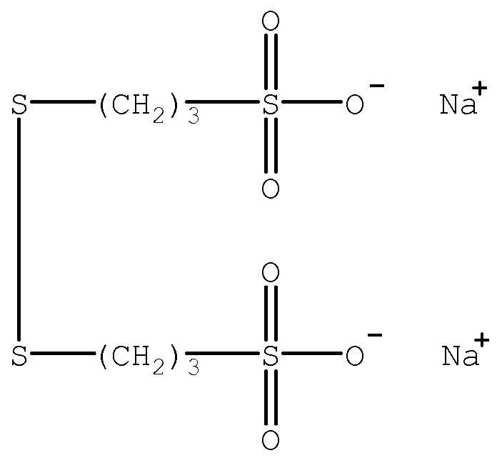
- organic sulfur compound of structure (2) is the sodium salt of 3,3'-dithiobis(l-propanesulfonate), which has the following structure (3):
- organic sulfur compound of structure (2) is 3,3'-dithiobis(l-propanesulfonic acid), which has the following structure (4):
- the organic sulfur compound may be added in a concentration between about 1 PPM and about 2 PPM typically between about 3 PPM and about 100 PPM, such as between about 5 PPM and 50 PPM.
- the organic sulfur compound is 3,3'-dithiobis(l-propanesulfonic acid) added in a concentration of about 20 PPM, which is between about 10 PPM and about 30 PPM.
- the electrolytic copper deposition composition comprises a component that polarizes the potential of copper deposition and yields a slower copper deposition rate near the opening of a through silicon via feature.
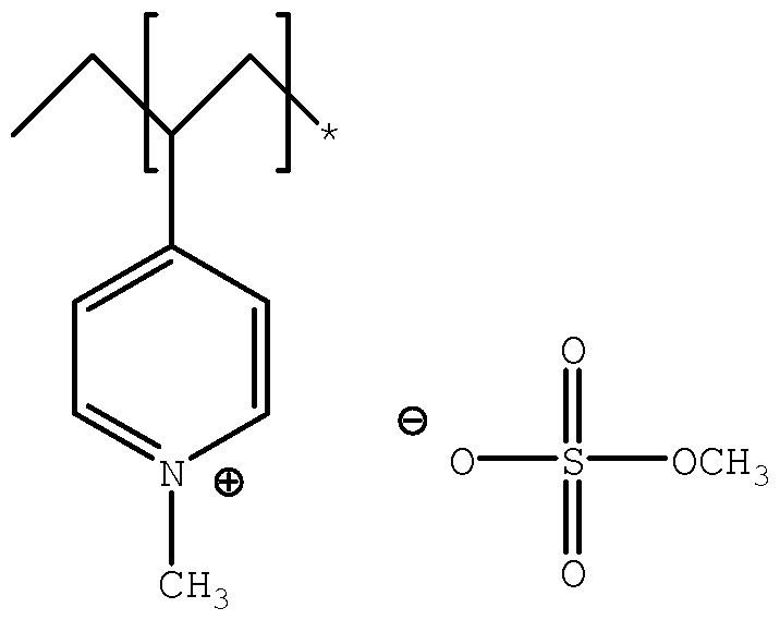
- An exemplary group of compounds observed to have a polarizing effect include vinyl-pyridine based compounds.
- the compound is a pyridinium compound and, in particular, a quaternized pyridinium salt.
- a pyridinium compound is a compound derived from pyridine in which the nitrogen atom of the pyridine is protonated.
- a quaternized pyridinium salt is distinct from pyridine, and quaternized pyridinium salt-based polymers are distinct from pyridine-based polymers, in that the nitrogen atom of the pyridine ring is quaternized in the quaternized pyridinium salt and quaternized pyridinium salt-based polymers.
- the suppressive compounds of the invention include derivatives of a vinyl pyridine, such as derivatives of 2-vinyl pyridine and, in certain preferred embodiments, derivatives of A- vinyl pyridine.
- the suppressive compound polymers of the invention encompass homo- polymers of vinyl pyridine, co-polymers of vinyl pyridine, quaternized salts of vinyl pyridine, and quaternized salts of these homo-polymers and co-polymers.
- Some specific examples of such compounds include, for example, poly(4-vinyl pyridine), the reaction product of poly(4-vinyl pyridine) with dimethyl sulfate, the reaction product of 4-vinyl pyridine with 2-chloroethanol, the reaction product of 4-vinyl pyridine with benzylchloride, the reaction product of 4-vinyl pyridine with allyl chloride, the reaction product of 4-vinyl pyridine with 4-chloromethylpyridine, the reaction product of 4-vinyl pyridine with 1,3 -propane sultone, the reaction product of 4-vinyl pyridine with methyl tosylate, the reaction product of 4-vinyl pyridine with chloroacetone, the reaction product of 4-vinyl pyridine with 2-methoxyethoxymethylchloride, the reaction product of 4-vinyl pyridine with 2-chloroethylether, the reaction product of 2-vinyl pyridine with methyl tosylate, the reaction product of 2-viny
- the molecular weight of the substituted pyridyl polymer compound additives of the invention in one embodiment is on the order of about 160,000 g/mol or less. While some higher molecular weight compounds are difficult to dissolve into the electroplating bath or to maintain in solution, other higher molecular weight compounds are soluble due to the added solubilizing ability of the quaternary nitrogen cation.
- solubility in this context is reference to relative solubility, such as, for example, greater than 60% soluble, or some other minimum solubility that is effective under the circumstances. It is not a reference to absolute solubility.
- the foregoing preference of 160,000 g/mol or less in certain embodiments is not narrowly critical.
- the molecular weight of the substituted pyridyl polymer compound additive is about 150,000 g/mol, or less.
- the molecular weight of the substituted pyridyl polymer compound additive is at least about 500 g/mol.
- the molecular weight of the substituted pyridyl polymer compound additive may be between about 500 g/mol and about 150,000 g/mol, such as about 700 g/mol, about 1000 g/mol, and about 10,000 g/mol.
- the substituted pyridyl polymers selected are soluble in a Cu plating bath, retain their functionality under electrolytic conditions, and do not yield deleterious by-products under electrolytic conditions, at least neither immediately nor shortly thereafter.
- the compound is a reaction product of a vinyl pyridine or poly(vinyl pyridine)
- it is obtained by causing a vinyl pyridine or poly(vinyl pyridine) to react with an alkylating agent selected from among those which yield a product which is soluble, bath compatible, and effective for leveling.
- candidates are selected from among reaction products obtained by causing vinyl pyridine or poly(vinyl pyridine) to react with a compound of the following structure (17):
- Rl is alkyl, alkenyl, aralkyl, heteroarylalkyl, substituted alkyl, substituted alkenyl, substituted aralkyl, or substituted heteroarylalkyl; and L is a leaving group.
- a leaving group is any group that can be displaced from a carbon atom.
- weak bases are good leaving groups.
- Exemplary leaving groups are halides, methyl sulfate, tosylates, and the like.
- Rl is alkyl or substituted alkyl; preferably,
- Rl is substituted or unsubstituted methyl, ethyl, straight, branched or cyclic propyl, butyl, pentyl or hexyl; in one embodiment Rl is methyl, hydroxyethyl, acetylmethyl, chloroethoxyethyl or methoxyethoxymethyl.
- Rl is alkenyl; preferably, Rl is vinyl, propenyl, straight or branched butenyl, straight, branched or cyclic pentenyl or straight, branched, or cyclic hexenyl; in one embodiment Rl is propenyl.
- Rl is aralkyl or substituted aralkyl; preferably, Rl is benzyl or substituted benzyl, naphthylalkyl or substituted naphthylalkyl; in one embodiment Rl is benzyl or naphthylmethyl.
- Rl is heteroarylalkyl or substituted heteroarylalkyl; preferably, Rl is pyridylalkyl; particularly, Rl is pyridylmethyl.
- L is chloride, methyl sulfate (CH 3 SO 4 -), octyl sulfate (CsHi 8 SO 4 -), trifluoromethanesulfonate (CF3SO3-), chloroacetate (CH 2 ClC(O)O-), or tosylate (C 7 H 7 SO 3 -); preferably, L is methyl sulfate, chloride or tosylate.
- Water soluble initiators can be used to prepare polymers of vinyl pyridine, though they are not used in the currently preferred embodiments or in the working examples.
- Exemplary water soluble initiators are peroxides (e.g., hydrogen peroxide, benzoyl peroxide, peroxybenzoic acid, etc.) and the like, and water soluble azo initiators such as 4,4'-Azobis(4-cyanovaleric acid).
- the compound constitutes a component of a mixture of one of the above-described polymers with a quantity of a monomer which is, for example, a monomeric vinyl pyridine derivative compound.
- the mixture is obtained by quaternizing a monomer to yield a quaternized salt which then undergoes spontaneous polymerization.
- the quaternized salt does not completely polymerize; rather, it yields a mixture of the monomer and spontaneously generated polymer.
- 4-vinyl pyridine is quaternized by reaction with dimethyl sulfate, and spontaneous polymerization occurs according to the following reaction scheme (45-65°C):
- the monomer fraction is increased with an increase in amount of methanol used in the quaternization reaction; that is, the degree of spontaneous polymerization is decreased.
- the component that polarizes the copper deposition and renders a slower copper deposition rate near the opening of a via feature may be incorporated into the electroplating bath at concentrations between about 1 ppm and about 200 ppm.
- the component that suppresses the rate of copper deposition near the opening of a via feature may be added to the electrolytic copper deposition composition at concentrations between about 1 and about 40 ppm or higher, preferably between about 2 ppm and about 20 ppm.
- concentration of the component is optimally determined in view of the aspect ratio of the feature to be copper metallized.
- the concentration of the component is preferably near the lower end of the preferred range, such as between about 4.2 ppm and about 8.4 ppm (0.45 micromolar), such as about 5.6 ppm.
- the concentration of the component is preferably near the higher end of the preferred range, such as between about 9.8 ppm and about 14 ppm, such as about 11.2 ppm.
- the leveler concentration is preferably maintained near the lower end of the preferred range to avoid unnecessarily prolonging the fill time.
- Alternative depolarizers applicable for use in this invention include polypropylene glycol amine (PPGA), in particular, poly(propylene glycol)bis(2- aminopropyl ether)(400 g/mol) and low molecular weight polypropylene glycol (PPG). When employed, these are added in a concentration between about 5 ppm and about 60 ppm, typically between about 15 ppm and about 30 ppm.
- PPGA polypropylene glycol amine
- PPG low molecular weight polypropylene glycol
- the electrolytic baths include acid baths including mixed organic acid baths and alkaline baths.
- Exemplary electrolytic copper plating baths include copper fluoroborate, copper pyrophosphate, copper phosphonate, copper sulfate, and other copper metal complexes such as copper methane sulfonate.
- Preferred copper sources include copper sulfate in sulfuric acid solution and copper methane sulfonate in methane sulfonic acid solution.
- the copper source is copper methanesulfonate and the acid is methanesulfonic acid.
- the use of copper methanesulfonate as the copper source allows for greater concentrations of copper ions in the electrolytic copper deposition composition in comparison to other copper ion sources. Accordingly, the source of copper ion may be added to achieve copper ion concentrations greater than about 50 g/L, greater than about 90 g/L, or even greater than about 100 g/L, such as, for example about 110 g/L.
- the copper methane sulfonate is added to achieve a copper ion concentration between about 70 g/L and about 100 g/L.
- the copper concentration is optimally determined in view of the aspect ratio of the feature to be copper metallized.
- the concentration of the copper ion is added and maintained at the higher end of the preferred concentration range, such as between about 90 g/L and about 110 g/L, such as about 110 g/L.
- the concentration of the copper ion may be added and maintained at the lower end of the preferred concentration range, such as between about 80 g/L and about 100 g/L, such as about 90 g/L.
- the concentration of the copper ion is optimally decreased.
- the copper concentration may be increased in embodiments wherein the feature a relatively low aspect ratio.
- methane sulfonic acid and its derivative and other organic sulfonic acids as the electrolyte.
- methane sulfonic acid When methane sulfonic acid is added, its concentration may be between about 1 g/L and about 50 g/L, such as between about 5 g/L and about 25 g/L, such as about 20 g/L.
- Experimental evidence to date indicates that increased acidity advantageously plays a role in the copper metallization process.
- FIG. 6 shows three current-potential curves from cyclic voltammetric experiments, with MSA concentrations of 0, 2 g/L, and 4 g/L. In this experiment, both copper reduction and oxidation information were obtained. It is important to distinguish the anodic current and cathodic current. In plating terminology, when the current is positive (I > 0), it is called anodic current; when the current is negative (I ⁇ 0), it is called cathodic current or reduction current.
- the concentration of copper ion and acid may vary over wide limits; for example, from about 4 to about 70 g/L copper and from about 2 to about 225 g/L sulfuric acid.
- the compounds of the invention are suitable for use in distinct acid/copper concentration ranges, such as high acid/low copper systems, in low acid/high copper systems, and mid acid/high copper systems.
- the copper ion concentration can be on the order of 4 g/L to on the order of 30 g/L; and the acid concentration may be sulfuric acid in an amount of greater than about 100 g/L up to about 225 g/L.
- the copper ion concentration is about 17 g/L where the H 2 SO 4 concentration is about 180 g/L.
- the copper ion concentration can be between about 35 g/L and about 60 g/L, such as between about 38 g/L and about 42 g/L.
- the copper ion concentration can be between about 46 g/L and about 60 g/L, such as between about 48 g/L and about 52 g/L. (35 g/L copper ion corresponds to about 140 g/L CuSO4-5H2O copper sulfate pentahydrate.)
- the acid concentration in these systems is preferably less than about 100 g/L.
- the acid concentration can be between about 5 g/L and about 30 g/L, such as between about 10 g/L and about 15 g/L. In some low acid/high copper, the acid concentration can be between about 50 g/L and about 100 g/L, such as between about 75 g/L to about 85 g/L. In an exemplary low acid/high copper system, the copper ion concentration is about 40 g/L and the H 2 SO 4 concentration is about 10 g/L. In another exemplary low acid/high copper system, the copper ion concentration is about 50 g/L and the H 2 SO 4 concentration is about 80 g/L.
- the copper ion concentration can be on the order of 30 g/L to on the order of 60 g/L; and the acid concentration may be sulfuric acid in an amount of greater than about 50 g/L up to about 100 g/L. In one mid acid/high copper system, the copper ion concentration is about 50 g/L where the H 2 SO 4 concentration is about 80 g/L.
- Chloride ion may also be used in the bath at a level up to about 200 mg/L (about 200 ppm), preferably about 10 mg/L to about 90 mg/L (10 to 90 ppm), such as about 50 gm/L (about 50 ppm). Chloride ion is added in these concentration ranges to enhance the function of other bath additives. In particular, it has been discovered that the addition of chloride ion enhances void-free filling.
- FIG. 7 is a flow chart of the process steps in preparing a wafer-to- wafer stack or chip-to-wafer stack involving through silicon via metallization.
- the wafer substrate i.e., device wafer
- the electrolytic copper deposition solution of the present invention comprises a back surface, a front surface, and vias and through silicon vias, which are prepared by photolithography and etching methods as is conventionally known.
- the front surface refers to the active side of the device wafer substrate.
- vias and through silicon vias have openings that extend from the front surface of the wafer substrate to a depth defined by the length of their sidewalls.
- conventional photoresist material is applied to a cleaned and dried surface of a device wafer by spin coating.
- the photoresist may be soft-baked to remove excess solvent at a temperature between about 6O 0 C and about 100 0 C for about 5 to 30 minutes.
- the photoresist is exposed to ultraviolet light in a manner that defines the pattern of copper metallization.
- Exposed photoresist is then dissolved using a developer solution.
- the wafer and photoresist defining the copper metallization pattern is then hard-baked, typically between about 120 0 C and about 180 0 C for about 20 to 30 minutes.
- the exposed wafer is then etched by means known in the art to define a pattern of vias having sidewalls and bottoms.
- the front surface of the wafer substrate and the sidewalls and the bottoms of the vias are then coated with a barrier layer, which may be titanium nitride, tantalum, tantalum nitride, or ruthenium to inhibit copper diffusion.
- a barrier layer which may be titanium nitride, tantalum, tantalum nitride, or ruthenium to inhibit copper diffusion.
- the barrier layer is typically seeded with a seed layer of copper or other metal to initiate copper superfilling plating thereon.
- a copper seed layer may be applied by chemical vapor deposition (CVD), physical vapor deposition (PVD), or the like.
- CVD chemical vapor deposition
- PVD physical vapor deposition
- the vias having barrier layers and copper seed layers are then plated using the electrolytic copper deposition composition and method of the present invention.
- the wafer surface having TSV features therein may optionally be pretreated to ensure proper wetting of the vias with the Cu filling chemistry.
- An exemplary solution useful for degassing the wafer surface if MICROF AB® PW 1000, available from Enthone Inc. (West Haven, Conn.). After degassing, TSV features located in the wafer is copper metallized using the electrolytic copper deposition composition of the present invention.
- a cathode substrate and anode are electrically connected by wiring and, respectively, to a rectifier (power supply).
- the cathode substrate for direct or pulse current has a net negative charge so that copper ions in the solution are reduced at the cathode substrate forming plated copper metal on the cathode surface.
- An oxidation reaction takes place at the anode. This same oxidation reaction may take place at the cathode if periodic pulse reverse plating is used.
- the cathode and anode may be horizontally or vertically disposed in the tank.
- a pulse current, direct current, reverse periodic current, periodic pulse reverse current, step current or other suitable current may be employed.
- the temperature of the electrolytic solution may be maintained using a heater/cooler whereby electrolytic solution is removed from the holding tank and flows through the heater/cooler and then is recycled to the holding tank.
- the bath temperature is typically about room temperature such as about 20-27 0 C, but may be at elevated temperatures up to about 40 0 C or higher. It is preferred to use an anode to cathode ratio of about 1 : 1, but this may also vary widely from about 1 :4 to 4: 1.
- the process also uses mixing in the electrolytic plating tank which may be supplied by agitation or preferably by the circulating flow of recycle electrolytic solution through the tank.
- the method of the present invention employs a current density profile in which initiation preferably occurs at a relatively low current density and in which the current density is increased after a period of copper deposition. Relatively low current densities may be used initially typically to avoid depleting copper ion locally near the bottom of the feature faster than the copper ion may be replenished.
- Optimal initial current densities and durations are typically determined experimentally and may vary depending upon the aspect ratio of the through silicon via feature. Increasing the initial relatively low current density to a relatively higher final current density may be continuous or according to a stepped profile. For example, in one embodiment, the current density may be stepped from an initiating current density to a second current density and stepped again to a final maximum current density. In one embodiment, there may be more than two current density steps, such as three, four, five, or more current density steps. Overall the current density averages between about 0.3 A/dm 2 and about 3 A/dm 2 .
- An exemplary stepped current density profile according to the method of the present invention may be as follows:
- This may involve one or more than one step, such as a step to 0.6 A/dm 2 , followed by a step to 0.7 A/dm 2 , followed by a step to about 0.8 A/dm 2 , followed by a step to about 0.9 A/dm 2 , followed by a step to about 1.0 A/dm 2 , followed by a step to about 1.1 A/dm 2 , followed by a step to about 1.2 A/dm 2 .
- the increase in current density in each step may be about 0.1 A/dm 2 , about 0.2 A/dm 2 , about 0.3 A/dm 2 , about 0.4 A/dm 2 , or more.
- the wafer surface and exposed copper metallization may be cleaned by chemical mechanical polishing, as is known in the art.
- the wafer may be thinned by conventional etching techniques to expose the bottom layer of copper metallization, thereby achieving through silicon via wherein copper metallization extends from the back surface of the wafer or IC die to the front, active surface of the wafer or die.
- the wafer may be further processed, stacked, and singulated by methods known in the art to achieve a device comprising multiple device levels, each connected electronically using through silicon via.
- An electrolytic copper deposition composition according to the present invention was prepared comprising the following components:
- the vias had an aspect ratio of 2.5: 1 (depth:opening diameter), resulting from an opening having a diameter of 100 microns and a total depth of 250 microns.
- the current density profile was characterized by relatively rapid increases to a maximum current density of 0.60 A/dm 2 .
- test wafer was degassed using MICROFAB® PW 1000
- the anode was a copper anode that was filmed prior to use in a copper methane sulfonate plating bath.
- the power supply supplied an average current density of 0.57 A/dm 2 .
- the current density was supplied according to the following stepped profile:
- FIGS. 8A and 8B are cross sections of the completely filled TSV features. Plating appears to occur according to a bottom-up mechanism since the TSV were void-free and seam-free.
- An electrolytic copper deposition composition according to the present invention was prepared comprising the following components:
- the vias had an aspect ratio of 1.75:1; 2.16: 1; 3: 1; and 5: 1
- the current density profile was characterized by relatively rapid increases to a maximum current density of 1.4 A/dm 2 .
- the test wafer was degassed using MICROFAB® PW 1000 (available from Enthone Inc., West Haven, Conn.) and then immersed in the electrolytic copper deposition composition.
- the anode was a copper anode that was filmed prior to use in a copper methane sulfonate plating bath.
- the power supply supplied an average current density of 0.84 A/dm 2 .
- the current density was supplied according to the following stepped profile:
- FIGS. 9 A, B, C, and D are FIB (Focused Ion Beam) cross sections of the completely filled TSV features. Plating appears to occur according to a bottom-up mechanism since the TSV were void- free and seam-free.
- Electrolytic Copper Deposition using an Electrolytic Copper Deposition Composition of the Present Invention was prepared comprising the following components:
- the vias had an aspect ratio of 3.5: 1; 3.8: 1; 2.5: 1; and 5: 1 (depth: opening diameter), resulting from an opening having the following diameters respectively: 50; 45; 75; 35 microns; and all having a depth of 175 microns.
- the current density profile was characterized by relatively rapid increases to a maximum current density of 1.2 A/dm .
- test wafer was degassed using MICROFAB® PW 1000 (available from Enthone Inc., West Haven, Conn.) and then immersed in the electrolytic copper deposition composition.
- the anode was a copper anode that was filmed prior to use in a copper methane sulfonate plating bath.
- the power supply supplied an average current density of 0.93 A/dm 2 .
- the current density was supplied according to the following stepped profile:
- FIGS. 1OA, B, C, and D are optical cross sections of the completely filled TSV features. Plating appears to occur according to a bottom-up mechanism since the TSV were void-free and seam-free.
- An electrolytic copper deposition composition having a composition:
- An electrolytic copper deposition composition according to the present invention was prepared comprising the following components:
- the vias had an aspect ratio of 3.5: 1; 2.5: 1 (depth: opening diameter), resulting from an opening having the following diameters respectively: 50; 75 microns; and each having a depth of 175 microns.
- the current density profile was characterized by relatively rapid increases to a maximum current density of 1.2 A/dm 2 .
- the test wafer was degassed using MICROFAB® PW 1000 (available from Enthone Inc., West Haven, Conn.) and then immersed in the electrolytic copper deposition composition.
- the anode was a copper anode that was filmed prior to use in a copper methane sulfonate plating bath.
- the power supply supplied an average current density of 0.93 A/dm 2 .
- the current density was supplied according to the following stepped profile:
- FIGS. 1 IA and B are optical cross sections of the completely filled TSV features. Plating appears to occur according to a bottom-up mechanism since the TSV were void-free and seam-free.
- An electrolytic copper deposition composition according to the present invention was prepared comprising the following components:
- Synalox 40-D700 (0.2 g/L) (random EO/PO copolymer available from Dow Chemical; m.w. 5300)
- Example 6 Electrolytic Copper Deposition using an Electrolytic Copper Deposition Composition of the Present Invention
- the electrolytic copper deposition composition of Example 5 was used to deposit copper metallization into a large size via in a test wafer substrate.
- the vias had an opening having a diameter of 50 microns and a total depth of 135 microns.
- the test wafer was degassed using MICROFAB® PW 1000 (available from Enthone Inc., West Haven, Conn.) and then immersed in the electrolytic copper deposition composition of Example 5.
- the anode was a copper anode that was filmed prior to use in a copper methane sulfonate plating bath.
- the power supply supplied an average current density of 0.50 A/dm2.
- the current density was supplied according to the following stepped profile:
- FIGS. 12A and 12B are optical photographs (500X magnification) of filled TSV features. Plating appears to occur according to a bottom-up mechanism since void-free and seam-free copper filled TSV were obtained.
- An electrolytic copper deposition composition according to the present invention was prepared comprising the following components:
- MIROFAB DVF200 C Metal quaternized poly(vinyl-4-pyridine) (4 mL/L).
- Example 7 The electrolytic copper deposition composition of Example 7 was used to deposit copper metallization into a large size via in a test wafer substrate.
- the vias had an opening having a diameter of 50 microns and a total depth of 200 microns.
- test wafer was degassed using MICROFAB® PW 1000 (available from Enthone Inc., West Haven, Conn.) and then immersed in the electrolytic copper deposition composition of Example 7.
- the anode was a copper anode that was filmed prior to use in a copper methane sulfonate plating bath.
- the power supply supplied an average current density of 0.64 A/dm 2 .
- the current density was supplied according to the following stepped profile:
- FIGS. 13A and 13B are optical photographs (500X magnification) of the partially filled TSV features. Plating appears to occur according to a true bottom-up mechanism as indicated by the "U" shaped plating profile.
- Example 9 Electrolytic Copper Deposition using an Electrolytic Copper Deposition Composition of the Present Invention
- the electrolytic copper deposition composition of Example 7 was used to deposit copper metallization into a large size via in a test wafer substrate.
- the vias had an aspect ratio of 3: 1 (depth: opening diameter), resulting from an opening having a diameter of 50 microns and a total depth of 150 microns.
- the current density profile was characterized by relatively rapid increases to a maximum current density of 0.60 A/dm 2 .
- the test wafer was degassed using MICROFAB® PW 1000 (available from Enthone Inc., West Haven, Conn.) and then immersed in the electrolytic copper deposition composition of Example 7.
- the anode was a copper anode that was filmed prior to use in a copper methane sulfonate plating bath.
- the power supply supplied an average current density of 0.58 A/dm 2 .
- the current density was supplied according to the following stepped profile:
- FIGS. 14A and 14B are optical photographs (200X magnification) of the completely filled TSV features. Plating appears to occur according to a bottom-up mechanism since the TSV were void-free and seam- free.
- An electrolytic copper deposition composition having a composition identical to that of Example 7 except for an increase in the concentration of the methyl quaternized poly(vinyl-4-pyridine) to 8 mL/L was used to deposit copper metallization into a large size, high aspect ratio via in a test wafer substrate.
- the vias had an aspect ratio of 4: 1 (depth: opening diameter), resulting from an opening having a diameter of 50 microns and a total depth of 200 microns.
- the current density profile was characterized by relatively rapid increases to a maximum current density of 0.60 A/dm 2 .
- the test wafer was degassed using MICROFAB® PW 1000 (available from Enthone Inc., West Haven, Conn.) and then immersed in the electrolytic copper deposition composition.
- the anode was a copper anode that was filmed prior to use in a copper methane sulfonate plating bath.
- the power supply supplied an average current density of 0.64 A/dm 2 .
- the current density was supplied according to the following stepped profile:
- FIGS. 15A and 15B are optical photographs (200X magnification) of the completely filled TSV features. Plating appears to occur according to a bottom-up mechanism since the TSV were void- free and seam-free.
- An electrolytic copper deposition composition comprising superfilling additives was prepared comprising the following components:
- H 2 SO 4 sulfuric acid, 80 g/L
- chloride ion 50 ppm
- MICROFAB® DVF 100 Additives available from Enthone Inc., West Haven, Conn.
- MICROFAB® DVF 100 A( 10 mL/L) [00193 ] MICROFAB® DVF 100 S (2 mL/L) [00194 ] MICROFAB® DVF 100 L (4 mL/L)
- the electrolytic copper deposition composition of Comparative Example 1 was used to deposit copper metallization into a large size via in a test wafer substrate.
- the via had an opening having a diameter of 50 microns and a total depth of 150 microns.
- the current density was relatively low to ensure good initiation, bottom up filling, and defect- free metallization.
- the test wafer was degassed using MICROFAB® PW 1000 (available from Enthone Inc., West Haven, Conn.) and then immersed in the electrolytic copper deposition composition of Comparative Example 1.
- the anode was a copper anode that was filmed prior to use in a copper sulfate plating bath.
- the power supply supplied a current density of 0.11 A/dm and plating was discontinued after five hours.
- FIG. 16 is an optical photograph (500X magnification) of the partially filled TSV feature. It is apparent from FIG. 16 that 5 hours of plating at this current density was not sufficient to metallize the entire feature. In fact, the feature was only about 33% filled.
- An electrolytic copper deposition composition comprising superfilling additives was prepared comprising the following components:
- MICROFAB® DVF 100 A (6 mL/L)
- MICROFAB® DVF 100 S (2 mL/L)
- MICROFAB® DVF 100 L (3 mL/L).
- the electrolytic copper deposition composition of Comparative Example 3 was used to deposit copper metallization into a large size via in a test wafer substrate.
- the via had an opening having a diameter of 50 microns and a total depth of 150 microns.
- the current density was relatively low to ensure good initiation, bottom up filling, and defect- free metallization.
- the test wafer was degassed using MICROFAB® PW 1000 (available from Enthone Inc., West Haven, Conn.) and then immersed in the electrolytic copper deposition composition of Comparative Example 3.
- the anode was a copper anode that was filmed prior to use in a copper sulfate plating bath.
- the power supply supplied a current density of 0.11 A/dm 2 and plating continued until the feature was completely filled with copper metal.
- FIG. 17 is an optical photograph (500X magnification) of the filled TSV feature. Deposition was characterized by bottom up growth, and the metallization was void-free and defect- free. The plating rate in the vertical direction was very slow however, about 0.27 microns/minute, and although the metallized feature was defect-free, filling the entire feature took 10 hours.
Landscapes
- Engineering & Computer Science (AREA)
- Chemical & Material Sciences (AREA)
- Metallurgy (AREA)
- Chemical Kinetics & Catalysis (AREA)
- Organic Chemistry (AREA)
- Materials Engineering (AREA)
- Electrochemistry (AREA)
- Microelectronics & Electronic Packaging (AREA)
- Condensed Matter Physics & Semiconductors (AREA)
- Power Engineering (AREA)
- General Physics & Mathematics (AREA)
- Computer Hardware Design (AREA)
- Physics & Mathematics (AREA)
- Manufacturing & Machinery (AREA)
- Electrodes Of Semiconductors (AREA)
- Electroplating Methods And Accessories (AREA)
- Electroplating And Plating Baths Therefor (AREA)
- Internal Circuitry In Semiconductor Integrated Circuit Devices (AREA)
Abstract
Description


Claims

Priority Applications (4)
| Application Number | Priority Date | Filing Date | Title |
|---|---|---|---|
| CN2008801097952A CN101855714B (en) | 2007-08-02 | 2008-08-04 | Copper metallization of through silicon via |
| KR1020107004714A KR101529342B1 (en) | 2007-08-02 | 2008-08-04 | Copper metallization of through silicon via |
| EP08797141.2A EP2183769B8 (en) | 2007-08-02 | 2008-08-04 | Copper metallization of through silicon via |
| JP2010519274A JP2010535289A (en) | 2007-08-02 | 2008-08-04 | Copper metal coating on through silicon vias |
Applications Claiming Priority (4)
| Application Number | Priority Date | Filing Date | Title |
|---|---|---|---|
| US95360207P | 2007-08-02 | 2007-08-02 | |
| US60/953,602 | 2007-08-02 | ||
| US5903908P | 2008-06-05 | 2008-06-05 | |
| US61/059,039 | 2008-06-05 |
Publications (1)
| Publication Number | Publication Date |
|---|---|
| WO2009018581A1 true WO2009018581A1 (en) | 2009-02-05 |
Family
ID=40304935
Family Applications (1)
| Application Number | Title | Priority Date | Filing Date |
|---|---|---|---|
| PCT/US2008/072136 WO2009018581A1 (en) | 2007-08-02 | 2008-08-04 | Copper metallization of through silicon via |
Country Status (7)
| Country | Link |
|---|---|
| US (1) | US7670950B2 (en) |
| EP (1) | EP2183769B8 (en) |
| JP (1) | JP2010535289A (en) |
| KR (1) | KR101529342B1 (en) |
| CN (1) | CN101855714B (en) |
| TW (1) | TWI341554B (en) |
| WO (1) | WO2009018581A1 (en) |
Cited By (6)
| Publication number | Priority date | Publication date | Assignee | Title |
|---|---|---|---|---|
| WO2010094998A1 (en) * | 2009-02-17 | 2010-08-26 | Atotech Deutschland Gmbh | Process for electrodeposition of copper chip to chip, chip to wafer and wafer to wafer interconnects in through-silicon vias (tsv) |
| WO2011102276A1 (en) * | 2010-02-22 | 2011-08-25 | Jx日鉱日石金属株式会社 | Aqueous solution of high purity copper sulfonate, and method for producing same |
| WO2011154493A1 (en) | 2010-06-11 | 2011-12-15 | Alchimer | Copper-electroplating composition and process for filling a cavity in a semiconductor substrate using this composition |
| JP2013028821A (en) * | 2010-11-18 | 2013-02-07 | Chiracol Co Ltd | Electrolytic copper plating bath for semiconductor and electrolytic copper plating method |
| EP2668317A1 (en) * | 2011-01-26 | 2013-12-04 | Enthone, Inc. | Process for filling vias in the microelectronics |
| US8884083B2 (en) | 2011-02-21 | 2014-11-11 | E. I. Du Pont De Nemours And Company | Selective catalytical dehydrochlorination of hydrochlorofluorocarbons |
Families Citing this family (49)
| Publication number | Priority date | Publication date | Assignee | Title |
|---|---|---|---|---|
| US7776741B2 (en) | 2008-08-18 | 2010-08-17 | Novellus Systems, Inc. | Process for through silicon via filing |
| US8388824B2 (en) * | 2008-11-26 | 2013-03-05 | Enthone Inc. | Method and composition for electrodeposition of copper in microelectronics with dipyridyl-based levelers |
| US9406561B2 (en) * | 2009-04-20 | 2016-08-02 | International Business Machines Corporation | Three dimensional integrated circuit integration using dielectric bonding first and through via formation last |
| US9677188B2 (en) | 2009-06-17 | 2017-06-13 | Novellus Systems, Inc. | Electrofill vacuum plating cell |
| US9455139B2 (en) | 2009-06-17 | 2016-09-27 | Novellus Systems, Inc. | Methods and apparatus for wetting pretreatment for through resist metal plating |
| US8962085B2 (en) | 2009-06-17 | 2015-02-24 | Novellus Systems, Inc. | Wetting pretreatment for enhanced damascene metal filling |
| US20110042803A1 (en) * | 2009-08-24 | 2011-02-24 | Chen-Fu Chu | Method For Fabricating A Through Interconnect On A Semiconductor Substrate |
| EP2483454A2 (en) | 2009-09-28 | 2012-08-08 | Basf Se | Copper electroplating composition |
| US10472730B2 (en) | 2009-10-12 | 2019-11-12 | Novellus Systems, Inc. | Electrolyte concentration control system for high rate electroplating |
| US9109295B2 (en) | 2009-10-12 | 2015-08-18 | Novellus Systems, Inc. | Electrolyte concentration control system for high rate electroplating |
| KR101302564B1 (en) * | 2009-10-28 | 2013-09-02 | 한국전자통신연구원 | Method of forming a via and method of fabricating chip stack package thereof |
| KR101300587B1 (en) * | 2009-12-09 | 2013-08-28 | 한국전자통신연구원 | Method for forming semiconductor device |
| US9138784B1 (en) | 2009-12-18 | 2015-09-22 | Novellus Systems, Inc. | Deionized water conditioning system and methods |
| US8992757B2 (en) | 2010-05-19 | 2015-03-31 | Novellus Systems, Inc. | Through silicon via filling using an electrolyte with a dual state inhibitor |
| TWI572750B (en) | 2010-05-24 | 2017-03-01 | 安頌股份有限公司 | Copper filling of through silicon vias |
| US20120024713A1 (en) * | 2010-07-29 | 2012-02-02 | Preisser Robert F | Process for electrodeposition of copper chip to chip, chip to wafer and wafer to wafer interconnects in through-silicon vias (tsv) with heated substrate and cooled electrolyte |
| US8404588B2 (en) | 2010-10-06 | 2013-03-26 | Electronics And Telecommunications Research Institute | Method of manufacturing via electrode |
| US9190371B2 (en) | 2010-12-21 | 2015-11-17 | Moon J. Kim | Self-organizing network with chip package having multiple interconnection configurations |
| KR101705734B1 (en) * | 2011-02-18 | 2017-02-14 | 삼성전자주식회사 | Copper electroplating solution and method of copper electroplating using the same |
| EP2518187A1 (en) * | 2011-04-26 | 2012-10-31 | Atotech Deutschland GmbH | Aqueous acidic bath for electrolytic deposition of copper |
| EP2530102A1 (en) | 2011-06-01 | 2012-12-05 | Basf Se | Additive and composition for metal electroplating comprising an additive for bottom-up filling of though silicon vias |
| WO2012164509A1 (en) | 2011-06-01 | 2012-12-06 | Basf Se | Composition for metal electroplating comprising an additive for bottom-up filling of though silicon vias and interconnect features |
| EP2560196A1 (en) | 2011-08-15 | 2013-02-20 | Nederlandse Organisatie voor toegepast -natuurwetenschappelijk onderzoek TNO | Method and system for forming a metallic structure |
| US8383460B1 (en) * | 2011-09-23 | 2013-02-26 | GlobalFoundries, Inc. | Method for fabricating through substrate vias in semiconductor substrate |
| CN102443828B (en) * | 2011-09-23 | 2014-11-19 | 上海华力微电子有限公司 | Method for electro-coppering in through hole of semiconductor silicon chip |
| US20130178063A1 (en) * | 2012-01-11 | 2013-07-11 | United Microelectronics Corp. | Method of manufacturing semiconductor device having silicon through via |
| US9330975B2 (en) | 2012-05-31 | 2016-05-03 | Micron Technology, Inc. | Integrated circuit substrates comprising through-substrate vias and methods of forming through-substrate vias |
| US8563403B1 (en) | 2012-06-27 | 2013-10-22 | International Business Machines Corporation | Three dimensional integrated circuit integration using alignment via/dielectric bonding first and through via formation last |
| CN103839872A (en) * | 2012-11-21 | 2014-06-04 | 中芯国际集成电路制造(上海)有限公司 | Method for manufacturing semiconductor device |
| US9613833B2 (en) | 2013-02-20 | 2017-04-04 | Novellus Systems, Inc. | Methods and apparatus for wetting pretreatment for through resist metal plating |
| CN103290438B (en) * | 2013-06-25 | 2015-12-02 | 深圳市创智成功科技有限公司 | For copper electroplating solution and the electro-plating method of wafer-level packaging |
| CN103361694A (en) * | 2013-08-08 | 2013-10-23 | 上海新阳半导体材料股份有限公司 | Micro-pore electroplated copper filling method for three-dimensional (3D) copper interconnection high aspect ratio through-silicon-via technology |
| CN103397354B (en) * | 2013-08-08 | 2016-10-26 | 上海新阳半导体材料股份有限公司 | A kind of additive in cavity after reducing silicon through hole technology copper facing annealing |
| US9435049B2 (en) | 2013-11-20 | 2016-09-06 | Lam Research Corporation | Alkaline pretreatment for electroplating |
| US9642261B2 (en) * | 2014-01-24 | 2017-05-02 | Zhuhai Advanced Chip Carriers & Electronic Substrate Solutions Technologies Co. Ltd. | Composite electronic structure with partially exposed and protruding copper termination posts |
| US9809891B2 (en) | 2014-06-30 | 2017-11-07 | Rohm And Haas Electronic Materials Llc | Plating method |
| US9481942B2 (en) | 2015-02-03 | 2016-11-01 | Lam Research Corporation | Geometry and process optimization for ultra-high RPM plating |
| US9617648B2 (en) | 2015-03-04 | 2017-04-11 | Lam Research Corporation | Pretreatment of nickel and cobalt liners for electrodeposition of copper into through silicon vias |
| US20160348245A1 (en) * | 2015-05-28 | 2016-12-01 | Macdermid, Incorporated | Method of Pretreatment for Electroless Plating |
| EP3317437B1 (en) | 2015-06-30 | 2023-09-13 | MacDermid Enthone Inc. | Cobalt filling of interconnects in microelectronics |
| US10988852B2 (en) | 2015-10-27 | 2021-04-27 | Rohm And Haas Electronic Materials Llc | Method of electroplating copper into a via on a substrate from an acid copper electroplating bath |
| WO2017090161A1 (en) * | 2015-11-26 | 2017-06-01 | 近藤 和夫 | Acidic copper plating solution, acidic copper plated product, and method for producing semiconductor device |
| US11035048B2 (en) * | 2017-07-05 | 2021-06-15 | Macdermid Enthone Inc. | Cobalt filling of interconnects |
| US10692735B2 (en) | 2017-07-28 | 2020-06-23 | Lam Research Corporation | Electro-oxidative metal removal in through mask interconnect fabrication |
| US10566287B1 (en) | 2018-02-02 | 2020-02-18 | Inphi Corporation | Light engine based on silicon photonics TSV interposer |
| TWI734362B (en) | 2019-01-31 | 2021-07-21 | 美商麥克達米德恩索龍股份有限公司 | Composition and method for fabrication of nickel interconnects |
| US11387191B2 (en) * | 2019-07-18 | 2022-07-12 | Taiwan Semiconductor Manufacturing Company, Ltd. | Integrated circuit package and method |
| JP7358251B2 (en) * | 2020-01-17 | 2023-10-10 | 株式会社荏原製作所 | Plating support system, plating support device, plating support program, and method for determining plating conditions |
| US11165509B1 (en) | 2020-06-05 | 2021-11-02 | Marvell Asia Pte, Ltd. | Method for co-packaging light engine chiplets on switch substrate |
Citations (3)
| Publication number | Priority date | Publication date | Assignee | Title |
|---|---|---|---|---|
| US20040082756A1 (en) * | 2002-06-27 | 2004-04-29 | Recai Sezi | Poly-o-hydroxyamide, polybenzoxazole from the poly-o-hydroxyamide, electronic component including a polybenzoxazole, and processes for producing the same |
| US20050045488A1 (en) * | 2002-03-05 | 2005-03-03 | Enthone Inc. | Copper electrodeposition in microelectronics |
| US20060141784A1 (en) * | 2004-11-12 | 2006-06-29 | Enthone Inc. | Copper electrodeposition in microelectronics |
Family Cites Families (54)
| Publication number | Priority date | Publication date | Assignee | Title |
|---|---|---|---|---|
| IT1046971B (en) * | 1975-03-11 | 1980-09-10 | Oxy Metal Industries Corp | Baths for electrodeposition of copper - contg soluble prod prepd by reacting alkoxylated polyalkylene-imine with alkylating agent |
| US4389505A (en) * | 1981-12-16 | 1983-06-21 | Mobil Oil Corporation | Plasticized polyacrylonitrile, a film thereof and a process for film preparation and plasticization |
| US6113771A (en) * | 1998-04-21 | 2000-09-05 | Applied Materials, Inc. | Electro deposition chemistry |
| US6793796B2 (en) * | 1998-10-26 | 2004-09-21 | Novellus Systems, Inc. | Electroplating process for avoiding defects in metal features of integrated circuit devices |
| US6544399B1 (en) * | 1999-01-11 | 2003-04-08 | Applied Materials, Inc. | Electrodeposition chemistry for filling apertures with reflective metal |
| JP3374130B2 (en) * | 1999-01-21 | 2003-02-04 | アトーテヒ ドイッチュラント ゲゼルシャフト ミット ベシュレンクテル ハフツング | Method for electrolytically forming high-purity copper conductor structures in integrated circuit fabrication |
| KR100665745B1 (en) * | 1999-01-26 | 2007-01-09 | 가부시키가이샤 에바라 세이사꾸쇼 | A method of copper plating and an apparatus therefor |
| US6444110B2 (en) * | 1999-05-17 | 2002-09-03 | Shipley Company, L.L.C. | Electrolytic copper plating method |
| US20040045832A1 (en) * | 1999-10-14 | 2004-03-11 | Nicholas Martyak | Electrolytic copper plating solutions |
| KR100659544B1 (en) * | 1999-11-12 | 2006-12-19 | 에바라 유지라이토 코포레이션 리미티드 | Via-filling process |
| JP2001181889A (en) * | 1999-12-22 | 2001-07-03 | Nippon Macdermid Kk | Bright tin-copper alloy electroplating bath |
| DE10013801A1 (en) * | 2000-03-20 | 2001-10-18 | Reinhardt Gmbh Maschbau | Sheet metal forming machine |
| US6706418B2 (en) * | 2000-07-01 | 2004-03-16 | Shipley Company L.L.C. | Metal alloy compositions and plating methods related thereto |
| US20020112964A1 (en) * | 2000-07-12 | 2002-08-22 | Applied Materials, Inc. | Process window for gap-fill on very high aspect ratio structures using additives in low acid copper baths |
| KR100366631B1 (en) * | 2000-09-27 | 2003-01-09 | 삼성전자 주식회사 | Electrolyte for copper plating comprising polyvinylpyrrolidone and electroplating method for copper wiring of semiconductor devices using the same |
| US6660153B2 (en) * | 2000-10-20 | 2003-12-09 | Shipley Company, L.L.C. | Seed layer repair bath |
| US6776893B1 (en) * | 2000-11-20 | 2004-08-17 | Enthone Inc. | Electroplating chemistry for the CU filling of submicron features of VLSI/ULSI interconnect |
| US6881319B2 (en) * | 2000-12-20 | 2005-04-19 | Shipley Company, L.L.C. | Electrolytic copper plating solution and method for controlling the same |
| US20050081744A1 (en) * | 2003-10-16 | 2005-04-21 | Semitool, Inc. | Electroplating compositions and methods for electroplating |
| US6740221B2 (en) * | 2001-03-15 | 2004-05-25 | Applied Materials Inc. | Method of forming copper interconnects |
| DE60226196T2 (en) * | 2001-05-24 | 2009-05-14 | Shipley Co., L.L.C., Marlborough | Tin-plating |
| US6551487B1 (en) * | 2001-05-31 | 2003-04-22 | Novellus Systems, Inc. | Methods and apparatus for controlled-angle wafer immersion |
| US6747217B1 (en) * | 2001-11-20 | 2004-06-08 | Unisys Corporation | Alternative to through-hole-plating in a printed circuit board |
| US7316772B2 (en) * | 2002-03-05 | 2008-01-08 | Enthone Inc. | Defect reduction in electrodeposited copper for semiconductor applications |
| US6926922B2 (en) * | 2002-04-09 | 2005-08-09 | Shipley Company, L.L.C. | PWB manufacture |
| JP2003328180A (en) * | 2002-05-17 | 2003-11-19 | Denso Corp | Method of filling plating into bottomed hole |
| EP1422320A1 (en) * | 2002-11-21 | 2004-05-26 | Shipley Company, L.L.C. | Copper electroplating bath |
| US7147767B2 (en) * | 2002-12-16 | 2006-12-12 | 3M Innovative Properties Company | Plating solutions for electrochemical or chemical deposition of copper interconnects and methods therefor |
| US20040154926A1 (en) * | 2002-12-24 | 2004-08-12 | Zhi-Wen Sun | Multiple chemistry electrochemical plating method |
| KR20040073974A (en) * | 2003-02-14 | 2004-08-21 | 롬 앤드 하스 일렉트로닉 머트어리얼즈, 엘.엘.씨. | Electroplating composition |
| US7105082B2 (en) * | 2003-02-27 | 2006-09-12 | Novellus Systems, Inc. | Composition and method for electrodeposition of metal on a work piece |
| US6924551B2 (en) * | 2003-05-28 | 2005-08-02 | Intel Corporation | Through silicon via, folded flex microelectronic package |
| US7111149B2 (en) * | 2003-07-07 | 2006-09-19 | Intel Corporation | Method and apparatus for generating a device ID for stacked devices |
| US20050274622A1 (en) * | 2004-06-10 | 2005-12-15 | Zhi-Wen Sun | Plating chemistry and method of single-step electroplating of copper on a barrier metal |
| JP2005033116A (en) * | 2003-07-11 | 2005-02-03 | Sony Corp | Via hole, semiconductor device having via hole, and forming method of same via hole |
| JP4624738B2 (en) * | 2003-08-21 | 2011-02-02 | 株式会社荏原製作所 | Plating equipment |
| US7049170B2 (en) * | 2003-12-17 | 2006-05-23 | Tru-Si Technologies, Inc. | Integrated circuits and packaging substrates with cavities, and attachment methods including insertion of protruding contact pads into cavities |
| CN1918327B (en) * | 2003-12-22 | 2010-08-25 | 恩索恩公司 | Copper electrodeposition in microelectronics |
| JP4540981B2 (en) * | 2003-12-25 | 2010-09-08 | 株式会社荏原製作所 | Plating method |
| US20050199507A1 (en) * | 2004-03-09 | 2005-09-15 | Taiwan Semiconductor Manufacturing Co., Ltd. | Chemical structures and compositions of ECP additives to reduce pit defects |
| US20050211564A1 (en) * | 2004-03-29 | 2005-09-29 | Taiwan Semiconductor Manufacturing Co., Ltd. | Method and composition to enhance wetting of ECP electrolyte to copper seed |
| DE102004029894B3 (en) * | 2004-06-17 | 2005-12-22 | Atotech Deutschland Gmbh | Apparatus and method for the electrolytic treatment of electrically mutually insulated, electrically conductive structures on surfaces of flat material to be treated |
| US7081408B2 (en) * | 2004-10-28 | 2006-07-25 | Intel Corporation | Method of creating a tapered via using a receding mask and resulting structure |
| JP4369348B2 (en) * | 2004-11-08 | 2009-11-18 | 新光電気工業株式会社 | Substrate and manufacturing method thereof |
| US20060264029A1 (en) * | 2005-05-23 | 2006-11-23 | Intel Corporation | Low inductance via structures |
| US7317256B2 (en) * | 2005-06-01 | 2008-01-08 | Intel Corporation | Electronic packaging including die with through silicon via |
| US20060278979A1 (en) * | 2005-06-09 | 2006-12-14 | Intel Corporation | Die stacking recessed pad wafer design |
| US7528006B2 (en) * | 2005-06-30 | 2009-05-05 | Intel Corporation | Integrated circuit die containing particle-filled through-silicon metal vias with reduced thermal expansion |
| US7405671B2 (en) * | 2005-07-01 | 2008-07-29 | Sebescak Andrew J | Power failure alarm |
| TWI328622B (en) * | 2005-09-30 | 2010-08-11 | Rohm & Haas Elect Mat | Leveler compounds |
| US7432592B2 (en) * | 2005-10-13 | 2008-10-07 | Intel Corporation | Integrated micro-channels for 3D through silicon architectures |
| US7410884B2 (en) * | 2005-11-21 | 2008-08-12 | Intel Corporation | 3D integrated circuits using thick metal for backside connections and offset bumps |
| US20070178697A1 (en) * | 2006-02-02 | 2007-08-02 | Enthone Inc. | Copper electrodeposition in microelectronics |
| US7575666B2 (en) * | 2006-04-05 | 2009-08-18 | James Watkowski | Process for electrolytically plating copper |
-
2008
- 2008-08-01 TW TW097129380A patent/TWI341554B/en active
- 2008-08-04 CN CN2008801097952A patent/CN101855714B/en active Active
- 2008-08-04 US US12/185,641 patent/US7670950B2/en active Active
- 2008-08-04 WO PCT/US2008/072136 patent/WO2009018581A1/en active Application Filing
- 2008-08-04 JP JP2010519274A patent/JP2010535289A/en active Pending
- 2008-08-04 KR KR1020107004714A patent/KR101529342B1/en active IP Right Grant
- 2008-08-04 EP EP08797141.2A patent/EP2183769B8/en active Active
Patent Citations (3)
| Publication number | Priority date | Publication date | Assignee | Title |
|---|---|---|---|---|
| US20050045488A1 (en) * | 2002-03-05 | 2005-03-03 | Enthone Inc. | Copper electrodeposition in microelectronics |
| US20040082756A1 (en) * | 2002-06-27 | 2004-04-29 | Recai Sezi | Poly-o-hydroxyamide, polybenzoxazole from the poly-o-hydroxyamide, electronic component including a polybenzoxazole, and processes for producing the same |
| US20060141784A1 (en) * | 2004-11-12 | 2006-06-29 | Enthone Inc. | Copper electrodeposition in microelectronics |
Non-Patent Citations (1)
| Title |
|---|
| See also references of EP2183769A4 * |
Cited By (10)
| Publication number | Priority date | Publication date | Assignee | Title |
|---|---|---|---|---|
| WO2010094998A1 (en) * | 2009-02-17 | 2010-08-26 | Atotech Deutschland Gmbh | Process for electrodeposition of copper chip to chip, chip to wafer and wafer to wafer interconnects in through-silicon vias (tsv) |
| JP2012518084A (en) * | 2009-02-17 | 2012-08-09 | アトテック ドイチェランド ゲーエムベーハー | Process for electrodeposition of chip-to-chip, chip-wafer and wafer-wafer copper interconnects in through-silicon vias (TSV) |
| WO2011102276A1 (en) * | 2010-02-22 | 2011-08-25 | Jx日鉱日石金属株式会社 | Aqueous solution of high purity copper sulfonate, and method for producing same |
| US8333834B2 (en) | 2010-02-22 | 2012-12-18 | Jx Nippon Mining & Metals Corporation | High-purity aqueous copper sulfonate solution and method of producing same |
| JP5384719B2 (en) * | 2010-02-22 | 2014-01-08 | Jx日鉱日石金属株式会社 | High purity copper sulfonate aqueous solution and method for producing the same |
| WO2011154493A1 (en) | 2010-06-11 | 2011-12-15 | Alchimer | Copper-electroplating composition and process for filling a cavity in a semiconductor substrate using this composition |
| JP2013028821A (en) * | 2010-11-18 | 2013-02-07 | Chiracol Co Ltd | Electrolytic copper plating bath for semiconductor and electrolytic copper plating method |
| EP2668317A1 (en) * | 2011-01-26 | 2013-12-04 | Enthone, Inc. | Process for filling vias in the microelectronics |
| EP2668317B1 (en) * | 2011-01-26 | 2017-08-23 | MacDermid Enthone Inc. | Process for filling vias in the microelectronics |
| US8884083B2 (en) | 2011-02-21 | 2014-11-11 | E. I. Du Pont De Nemours And Company | Selective catalytical dehydrochlorination of hydrochlorofluorocarbons |
Also Published As
| Publication number | Publication date |
|---|---|
| JP2010535289A (en) | 2010-11-18 |
| TWI341554B (en) | 2011-05-01 |
| EP2183769A1 (en) | 2010-05-12 |
| CN101855714A (en) | 2010-10-06 |
| KR101529342B1 (en) | 2015-06-19 |
| CN101855714B (en) | 2013-05-08 |
| EP2183769B1 (en) | 2017-07-19 |
| EP2183769A4 (en) | 2015-12-09 |
| KR20100055446A (en) | 2010-05-26 |
| EP2183769B8 (en) | 2017-08-23 |
| US20090035940A1 (en) | 2009-02-05 |
| TW200924036A (en) | 2009-06-01 |
| US7670950B2 (en) | 2010-03-02 |
Similar Documents
| Publication | Publication Date | Title |
|---|---|---|
| US7670950B2 (en) | Copper metallization of through silicon via | |
| EP1810322B1 (en) | Copper electrodeposition in microelectronics | |
| EP2668317B1 (en) | Process for filling vias in the microelectronics | |
| CN101416292B (en) | Copper electrodeposition in microelectronics | |
| US9493884B2 (en) | Copper electrodeposition in microelectronics | |
| US10988852B2 (en) | Method of electroplating copper into a via on a substrate from an acid copper electroplating bath | |
| JP7345586B2 (en) | Copper electrodeposition in microelectronics | |
| US9809891B2 (en) | Plating method | |
| TWI572750B (en) | Copper filling of through silicon vias |
Legal Events
| Date | Code | Title | Description |
|---|---|---|---|
| WWE | Wipo information: entry into national phase |
Ref document number: 200880109795.2 Country of ref document: CN |
|
| 121 | Ep: the epo has been informed by wipo that ep was designated in this application |
Ref document number: 08797141 Country of ref document: EP Kind code of ref document: A1 |
|
| WWE | Wipo information: entry into national phase |
Ref document number: 2010519274 Country of ref document: JP |
|
| NENP | Non-entry into the national phase |
Ref country code: DE |
|
| REEP | Request for entry into the european phase |
Ref document number: 2008797141 Country of ref document: EP |
|
| WWE | Wipo information: entry into national phase |
Ref document number: 2008797141 Country of ref document: EP |
|
| ENP | Entry into the national phase |
Ref document number: 20107004714 Country of ref document: KR Kind code of ref document: A |