WO2008150058A1 - Hardmask composition having antireflective properties and method of patterning material on substrate using the same - Google Patents

Hardmask composition having antireflective properties and method of patterning material on substrate using the same Download PDF

Info

Publication number
WO2008150058A1
WO2008150058A1 PCT/KR2007/007059 KR2007007059W WO2008150058A1 WO 2008150058 A1 WO2008150058 A1 WO 2008150058A1 KR 2007007059 W KR2007007059 W KR 2007007059W WO 2008150058 A1 WO2008150058 A1 WO 2008150058A1
Authority
WO
WIPO (PCT)
Prior art keywords
layer
hardmask
composition according
composition
weight
Prior art date
Legal status (The legal status is an assumption and is not a legal conclusion. Google has not performed a legal analysis and makes no representation as to the accuracy of the status listed.)
Ceased
Application number
PCT/KR2007/007059
Other languages
French (fr)
Inventor
Kyong Ho Yoon
Jong Seob Kim
Dong Seon Uh
Hwan Sung Cheon
Chang Il Oh
Min Soo Kim
Jin Kuk Lee
Current Assignee (The listed assignees may be inaccurate. Google has not performed a legal analysis and makes no representation or warranty as to the accuracy of the list.)
Cheil Industries Inc
Original Assignee
Cheil Industries Inc
Priority date (The priority date is an assumption and is not a legal conclusion. Google has not performed a legal analysis and makes no representation as to the accuracy of the date listed.)
Filing date
Publication date
Application filed by Cheil Industries Inc filed Critical Cheil Industries Inc
Priority to CN200780053206A priority Critical patent/CN101681096A/en
Priority to JP2010511100A priority patent/JP2010529499A/en
Publication of WO2008150058A1 publication Critical patent/WO2008150058A1/en
Anticipated expiration legal-status Critical
Ceased legal-status Critical Current

Links

Classifications

    • GPHYSICS
    • G03PHOTOGRAPHY; CINEMATOGRAPHY; ANALOGOUS TECHNIQUES USING WAVES OTHER THAN OPTICAL WAVES; ELECTROGRAPHY; HOLOGRAPHY
    • G03FPHOTOMECHANICAL PRODUCTION OF TEXTURED OR PATTERNED SURFACES, e.g. FOR PRINTING, FOR PROCESSING OF SEMICONDUCTOR DEVICES; MATERIALS THEREFOR; ORIGINALS THEREFOR; APPARATUS SPECIALLY ADAPTED THEREFOR
    • G03F7/00Photomechanical, e.g. photolithographic, production of textured or patterned surfaces, e.g. printing surfaces; Materials therefor, e.g. comprising photoresists; Apparatus specially adapted therefor
    • G03F7/004Photosensitive materials
    • G03F7/09Photosensitive materials characterised by structural details, e.g. supports, auxiliary layers
    • G03F7/091Photosensitive materials characterised by structural details, e.g. supports, auxiliary layers characterised by antireflection means or light filtering or absorbing means, e.g. anti-halation, contrast enhancement
    • GPHYSICS
    • G03PHOTOGRAPHY; CINEMATOGRAPHY; ANALOGOUS TECHNIQUES USING WAVES OTHER THAN OPTICAL WAVES; ELECTROGRAPHY; HOLOGRAPHY
    • G03FPHOTOMECHANICAL PRODUCTION OF TEXTURED OR PATTERNED SURFACES, e.g. FOR PRINTING, FOR PROCESSING OF SEMICONDUCTOR DEVICES; MATERIALS THEREFOR; ORIGINALS THEREFOR; APPARATUS SPECIALLY ADAPTED THEREFOR
    • G03F7/00Photomechanical, e.g. photolithographic, production of textured or patterned surfaces, e.g. printing surfaces; Materials therefor, e.g. comprising photoresists; Apparatus specially adapted therefor
    • G03F7/004Photosensitive materials
    • GPHYSICS
    • G03PHOTOGRAPHY; CINEMATOGRAPHY; ANALOGOUS TECHNIQUES USING WAVES OTHER THAN OPTICAL WAVES; ELECTROGRAPHY; HOLOGRAPHY
    • G03FPHOTOMECHANICAL PRODUCTION OF TEXTURED OR PATTERNED SURFACES, e.g. FOR PRINTING, FOR PROCESSING OF SEMICONDUCTOR DEVICES; MATERIALS THEREFOR; ORIGINALS THEREFOR; APPARATUS SPECIALLY ADAPTED THEREFOR
    • G03F7/00Photomechanical, e.g. photolithographic, production of textured or patterned surfaces, e.g. printing surfaces; Materials therefor, e.g. comprising photoresists; Apparatus specially adapted therefor
    • G03F7/004Photosensitive materials
    • G03F7/0045Photosensitive materials with organic non-macromolecular light-sensitive compounds not otherwise provided for, e.g. dissolution inhibitors
    • GPHYSICS
    • G03PHOTOGRAPHY; CINEMATOGRAPHY; ANALOGOUS TECHNIQUES USING WAVES OTHER THAN OPTICAL WAVES; ELECTROGRAPHY; HOLOGRAPHY
    • G03FPHOTOMECHANICAL PRODUCTION OF TEXTURED OR PATTERNED SURFACES, e.g. FOR PRINTING, FOR PROCESSING OF SEMICONDUCTOR DEVICES; MATERIALS THEREFOR; ORIGINALS THEREFOR; APPARATUS SPECIALLY ADAPTED THEREFOR
    • G03F7/00Photomechanical, e.g. photolithographic, production of textured or patterned surfaces, e.g. printing surfaces; Materials therefor, e.g. comprising photoresists; Apparatus specially adapted therefor
    • G03F7/004Photosensitive materials
    • G03F7/0047Photosensitive materials characterised by additives for obtaining a metallic or ceramic pattern, e.g. by firing
    • GPHYSICS
    • G03PHOTOGRAPHY; CINEMATOGRAPHY; ANALOGOUS TECHNIQUES USING WAVES OTHER THAN OPTICAL WAVES; ELECTROGRAPHY; HOLOGRAPHY
    • G03FPHOTOMECHANICAL PRODUCTION OF TEXTURED OR PATTERNED SURFACES, e.g. FOR PRINTING, FOR PROCESSING OF SEMICONDUCTOR DEVICES; MATERIALS THEREFOR; ORIGINALS THEREFOR; APPARATUS SPECIALLY ADAPTED THEREFOR
    • G03F7/00Photomechanical, e.g. photolithographic, production of textured or patterned surfaces, e.g. printing surfaces; Materials therefor, e.g. comprising photoresists; Apparatus specially adapted therefor
    • G03F7/004Photosensitive materials
    • G03F7/09Photosensitive materials characterised by structural details, e.g. supports, auxiliary layers
    • G03F7/11Photosensitive materials characterised by structural details, e.g. supports, auxiliary layers having cover layers or intermediate layers, e.g. subbing layers
    • YGENERAL TAGGING OF NEW TECHNOLOGICAL DEVELOPMENTS; GENERAL TAGGING OF CROSS-SECTIONAL TECHNOLOGIES SPANNING OVER SEVERAL SECTIONS OF THE IPC; TECHNICAL SUBJECTS COVERED BY FORMER USPC CROSS-REFERENCE ART COLLECTIONS [XRACs] AND DIGESTS
    • Y10TECHNICAL SUBJECTS COVERED BY FORMER USPC
    • Y10STECHNICAL SUBJECTS COVERED BY FORMER USPC CROSS-REFERENCE ART COLLECTIONS [XRACs] AND DIGESTS
    • Y10S438/00Semiconductor device manufacturing: process
    • Y10S438/942Masking
    • Y10S438/948Radiation resist
    • Y10S438/952Utilizing antireflective layer

Definitions

  • the present invention relates to a hardmask composition haying antirefiective properties suitable for lithography. More specifically, the present invention relates to a hardmask composition comprising one or more aromatic ring-containing polymers with a strong absorption in the short wavelength region (e ⁇ g., 157 nm, 193 nm and 248 nm).
  • Lithography affects the manufacture of microscopic structures from the viewpoint of direct imaging of patterns on particular substrates and production of masks typically used for such imaging.
  • a typical lithographic process involves patternwise exposure of a radiation-sensitive resist to imaging radiation to form a patterned resist layer. Thereafter, an, image is ⁇ developed by bringing the exposed resist layer into contact with a certain substance (typically, an aqueous alkaline developing solution), Then, the substance present in openings of the patterned resist, layer is etched to transfer a pattern to an underlying material. After completion of the transfer, remaining portions of the resist layer are removed.
  • a certain substance typically, an aqueous alkaline developing solution
  • an antireflective coating is used to minimize the reflectivity between an imaging layer, e>g., n radiation-sensitive resist material layer, and an underlying layer. Plowever, since many portions of the imaging layer are removed during etching of ARC after patterning, patterning may be further required in the subsequent etching step.
  • the resist does not provide resistance to the subsequent etching step to an extent sufficient to effectively transfer the desired pattern to a layer underlying the resist.
  • a so-called 'hardmask layer 1 is used as an intermediate layer between the patterned resist layer and the underlying material that can be patterned by transfer from the patterned resist.
  • the hardmask layer must be able to receive the pattern from the patterned resist layer and withstand etching required to transfer the pattern to the underlying material,
  • a hardmask composition that provides superior storage properties and avoids unwanted interactions (e.g ⁇ , acid pollution from a hardmask) with an imaging resist layer would further be desirable,
  • a hardmask composition that has particular optical properties against imaging radiation at shorter wavelengths ⁇ e.g., 157 nm, 193 nm, and 248 nm) would also be desirable.
  • an overlying hardmask layer formed by spin coating may have an isotropic (e.g., bowed) etch profile during dry etching, which makes it difficult to allow the hardmask layer to function as a hardmask of a relatively thick underlying layer.
  • Attempts have been made to prevent the occurrence of isotropic etch profiles, for example, by varying dry etching conditions.
  • device makers suffer from limitations in the operation of mass-production facilities. Under such circumstances, the present inventors have endeavored to prepare a high-density networking polymer with high carbon content in an amorphous structure that can be used to form a hardmask having an anisotropic profile.
  • the present invention has been made in view of the problems of the prior art, and it is one object of the present invention to provide a novel hardmask composition suitable for use in a lithographic process that exhibits high etch selectivity, is sufficiently resistant to multiple etching, and minimizes the reflectivity between a resist and an underlying layer.
  • an antireflective hardmask composition comprising [15] (a) at least one aromatic ring-containing polymer selected from the group consisting of polymers represented by formulae 1, 2 and 3:
  • each R x is selected from
  • R is H or alkyl
  • each R 2 is selected from hydrogen (-H), hydroxyl (-OH), C 1 -Ci 0 alkyl, C 6 -C 10 aryl, allyl and halogen
  • R 3 is selected from
  • R 4 is selected from
  • R 1 , R 2 , R 3 , R 4 , R 5 and n are as defined in Ibrmulae 1 and 2, 1 ⁇ m ⁇ 750, and 2 ⁇ m + n ⁇ 1,500, and
  • the hardmask composition of the present invention may further comprise (c) a cros slinking component.
  • the hardmask composition of the present invention may further comprise (d) an acid or base catalyst
  • the hardmask composition of the present invention may comprise 1 to 20% by weight of the aromatic ring-containing polymer (a), 75 to 98.8% by weight of the organic solvent (b), Ql to 5% by weight of the crosslinMng component (c), and QOOl to Q05% by weight of the acid or base catalyst (d).
  • the aromatic ring-containing polymer preferably has a weight average molecular weight of 1 ,000 to 30,00Q
  • the hardmask composition of the present invention may further comprise a surfactant
  • the crosslinking component may be selected from the group consisting of melamine resins, amino resins, glycoluril compounds, and bisepoxy compounds.
  • the acid catalyst may be selected from the group consisting of _p-toluenesulfonic acid monohydrate, pyridinium p-toluenesulfonate, 2,4,4,6-tetrabromocyclohexadienone, benzoin tosylate, 2-nitrobenzyl tosylate, and alkyl esters of organic sulfonic acids.
  • the method of the present invention comprises the steps of (a) providing a material layer on a substrate, (b) forming an antireflective hardmask layer using the composition on the material layer, (c) forming a radiation-sensitive imaging layer on the antireflective hardmask layer, (d) patternwise exposing the radiation-sensitive imaging layer to radiation to form a pattern of radiation-exposed regions in the imaging layer, (e) selectively removing portions of the radiation-sensitive imaging layer and the antireflective hardmask layer to expose portions of the material layer, and (f) etching the exposed portions of the material layer to pattern the material layer.
  • the method of the present invention may further comprise the step of forming a silicon-containing hardmask layer prior to step (c).
  • the method of the present invention may further comprise the step of forming a bottom antireflective coating (BARQ on the silicon-containing hardmask layer prior to step (c).
  • the present invention provides an antireflective hardmask composition characterized by the presence of one or more aromatic ring-containing polymers with a strong absorption in the short wavelength region (particularly, 248 nm or less).
  • the antireflective hardmask composition comprises (a) at least one aromatic ring-containing polymer having a strong absorption in the short wavelength region (particularly, 248 nm or less), which is selected from the group consisting of polymers represented by formulae 1, 2 and 3:
  • each R 1 is selected from
  • eachR2 is selected from hydrogen (-H), hydroxy! (-OH), C 1 -Ci 0 alkyl, C 6 -Ci 0 aryl, allyl and halogen, R 3 is selected from
  • R 5 is selected from
  • the aromatic ring-containing polymer (a) contains aromatic rings in the skeleton of the polymer. Since the aromatic rings absorb light of short wavelengths (248 nm or less) during lithography, the composition of the present invention can be used to form a hardmask layer that minimizes the reflectivity between a resist and an underlying layer, thus avoiding the formation of an additional antire- flective coating (ARQ.
  • ARQ antire- flective coating
  • the aromatic ring-containing polymer has a number of reactive sites (i.e. hydroxyl (-OH) groups) distributed along the backbone chain of the polymer that reacts with a crosslinking component.
  • hydroxyl groups react with the adjacent hydroxyl groups or the terminal alkoxy (-OCH 3 ) groups of the polymer ('self-crosslinkmg'). This self-crosslinking allows the antireflective hardmask composition of the present invention to be cured by baking without the use of an additional crosslinking component.
  • the curing of the composition according to the present invention may be promoted by crosslinking with a crosslinking component other than the selfcrosslinking. That is, a number of reactive sites (particularly, hydroxyl (-OH) groups) distributed along the backbone of the polymer can be crosslinked with a crosslinking component,
  • the antireflective hardmask composition of the present invention lias solution- and film-forming characteristics, which assist in the formation of a layer by a conventional spin-coating technique.
  • the aromatic ring-containing polymer preferably has a weight average molecular weight of 1,000 to 30,000 Within this range, the aromatic ring-containing polymer is appropriately soluble in the solvent, rendering the hardmask composition suitable for coating.
  • the aromatic ring-containing polymer (a) is preferably present in an amount of 1 to 30 parts by weight, based on 100 parts by weight of the organic solvent (b).
  • the reason why the amount of the aromatic ring-containing polymer used is limited within the range defined above is that a desired coating thickness is not attained, Le. it is difficult to accurately regulate a coating thickness.
  • organic solvent (b) there is no particular limitation on the kind of the organic solvent (b) so long as the aromatic ring-containing polymer (a) can be sufficiently dissolved in the organic solvent (b).
  • suitable organic solvents there may be exemplified propylene glycol monomethyl ether acetate (PGMEA), propylene glycol monomethyl ether (PGME), cyclohexanone (Anone) and ethyl lactate (EL).
  • the hardmask composition of the present invention may further comprise (c) a crosslinking component that is preferably capable of crosslinking the repeating units of the polymer upon heating.
  • the hardmask composition of the present invention may further comprise (d) an acid or base catalyst that preferably serves to catalyze the crosslinking component (c). It is more preferred that the catalyst (d) be thermally activated.
  • Any crosslinking component capable of reacting with the hydroxyl groups of the aromatic ring-containing polymer in a manner that can be catalyzed by the acid or base catalyst may be used without any particular limitation in the hardmask composition of the present invention.
  • suitable crosslinking components for use in the antireflective hardmask composition of the present invention include: etherified amino resins, methylated melamine resins (e.g,, N-methoxymethyl-melamine resins), butylated melamine resins (e.g., N-butoxymethyl-melamine resins), methylated and butylated urea resins (e.g., Cymel U-65 Resin and UFR 80 Resin), glycoluril derivatives (e.g., Powderlink 1174), and 2,6-bis(hydroxymethyl)-/?-cresol.
  • etherified amino resins e.g, methylated melamine resins (e.g, N-methoxymethyl-melamine resins), butylated melamine resins (e.g., N-butoxymethyl-melamine resins), methylated and butylated urea resins (e.g., Cymel U-65 Resin and UFR 80 Resin), glycoluril derivatives (e.
  • the Powderlink 1174 is a compound of Ramula 4:
  • crosslinking component there may be used the bisepoxy compound of formula 5:
  • Exemplary acid catalysts include organic acids, e.g,, p-toluenesulfonic acid monohydrate.
  • a thermal acid generator (TAG) may be used as the acid catalyst.
  • TAG is a compound that generates an acid upon thermal treatment.
  • preferred TAGs include pyridinium p-toluenes ⁇ lfonate, 2,4,4 ,6-tetrabromocyclohexadienol, benzoin tosylate, 2-nitrobenzyl tosylate, and alkyl esters of organic sulfonic acids.
  • the base catalyst may be selected from ammonium hydroxides represented by NH 4
  • the aromatic ring-containing polymer (a) is preferably present in an amount of 1 to 2C% by weight and more preferably 3 to 10% by weight
  • the organic solvent (b) is preferably present in an amount of 75 to 98.8% by weight
  • the crosslinking component (c) is preferably present in an amount of Ql to 5% by weight and more preferably Ql to 3% by weight
  • the acid or base catalyst (d) is preferably present in an amount of QOOl to Q05% by weight and more preferably QOOl to QQ3% by weight.
  • crosslinking component When the content of the crosslinking component is les s than Q 1 % by weight, crosslinking properties may be not exhibited. Meanwhile, when the content of the crosslinking component is greater than 5% by weight, deformation of a pattern profile may be caused and redeposition contamination may occur due to volatile components evolved upon baking.
  • the hardmask composition of the present invention may further comprise at least one additive, such as a surfactant.
  • the present invention also provides a method for patterning an underlying material layer on a substrate by using the hardmask composition.
  • the method of the present invention comprises the steps of (a) providing a material layer on a substrate, (b) forming an antireflective hardmask layer using the composition on the material layer, (c) forming a radiation-sensitive imaging layer on the antireflective hardmask layer, (d) patternwise exposing the radiation-sensitive imaging layer to radiation to form a pattern of radiation-exposed regions in the imaging layer, (e) selectively removing portions of the radiation-sensitive imaging layer and the hardmask layer to expose portions of the material layer, and (f) etching the exposed portions of the material layer to pattern the material layer.
  • the method may further comprise the step of forming a silicon-containing hardmask layer prior to step (c).
  • the method may further comprise the step of forming a bottom antireflective hardmask layer (BARQ on the silicon-containing hardmask layer prior to step (c).
  • the method of the present invention can be carried out in accordance with the following procedure.
  • a material e.g., aluminum or silicon nitride (SN)
  • the material may be an, electrically conductive, semi-conductive, magnetic or insulating material.
  • the hardmask composition of the present invention is spin-coated to a thickness of 500 to 8,000 and baked at 100-30CFC for 10 seconds to 10 minutes to form a hardmask layer.
  • a silicon-containing hardmask composition may be spin-coated to a thickness of 500 to 4,000 on the hardmask layer and baked at 100-3 OCPC for 10 seconds to 10 minutes to form a silicon-containing hardmask layer. If needed, a bottom antireflective coating (BARQ may be formed on the silicon- containing hardmask layer.
  • BARQ bottom antireflective coating
  • a radiation- sensitive image layer is formed on the hardmask layer.
  • Light exposure and development are performed to form a pattern on the imaging layer.
  • Dry etching is performed using a gas mixture, such as CHP 3 /CF 4 , through recessed portions of the patterned imaging layer to transfer the pattern to the silicon-containing hardmask layer.
  • a gas mixture such as BC1 3 /C1 2 , is used to etch the exposed portions of the hardmask layer through the patterned silicon hardmask layer as a mask. As a result, the hardmask layer is patterned.
  • Dry etching is performed using a gas mixture, such as CHF 3 /CF 4 , to pattern the material layer on the substrate. Ashing may be performed to remove the remaining material, leaving the patterned material layer only, for example, the removal of the remaining material can be accomplished using oxygen plasma.
  • the method of the present invention can be applied to the fabrication of a semiconductor integrated circuit device.
  • Each of the sample solutions prepared in Examples 1 to 4 was spin-coated on a silicon wafer and baked at 200 1 C for 60 seconds to form a 4,000A-thick film.
  • Each of the sample solutions prepared in Examples 1 to 4 was spin-coated on a silicon wafer covered with silicon nitride and baked at 200 1 C for 60 seconds to form a 4,000 A-thick film.
  • a silicon antireflective coating was formed on the film and baked at 240C for 60 seconds. Thereafter, an ArF photoresist (PR) was coated to a thickness of 1,XK) on the silicon ARC, baked at 1 ICPC for 60 seconds, exposed to light using an ArF exposure system (ASML, XT: 1400, NA Q93), and developed with an aqueous solution of TMAH (2.38 wt%) to form a 63-nm line and space pattern. The patterns were observed using a field emission scanning electron microscope (FE-SEM). The patterns were measured for exposure latitude (EL) margin as a function of exposure energy and depth of focus (DoF) margin as a function of the distance from a light source. The results are recorded in Table 2.
  • EL exposure latitude
  • DoF depth of focus
  • Each of the silicon ARCs of the patterned specimens was dry- etched using a gas mixture of CHF 3 /CF 4 through a photoresist (PR) as a mask.
  • the hardmaslc was dry-etched using a gas mixture OfO 2 ZN 2 through the silicon ARC as a mask.
  • the silicon nitr ⁇ e was dry-etched using a gas mixture OfCHF 3 ZCF 4 through the hardmask as a mask. O 2 ashing and wet stripping were performed on the remaining portions of the hardmask and the organic material.
  • the antiretlective hardmask composition of the present invention can be used to form a film having a refractive index and an ab- sorbance suitable for use as an antireflective film in the deep UV (DUV) (e.g., ArF (193 nm) and KrF (248 nm)). Therefore, the antireflective hardmask composition of the present invention exhibits -very high etch selectivity for lithography.
  • the antireflective hardmask composition of the present invention is sufficiently resistant to multiple etching, it can be used to form a hardmask having a very good etch profile. Therefore, a good image can be transferred to an underlying layer.
  • Fur- thermore since the antirefiective hardmask composition of the present invention can minimize the reflectivity between a resist and an underlying layer, it can be used to provide a lithographic structure that has better results in terms of pattern profile and margins.
  • the composition of the present invention and the resulting lithographic structure can be used in the fabrication and design of integrated circuit devices.
  • the composition of the present invention can be used in the formation of patterned material layer structures, such as metal wirings, holes for contacts and biases, insulating sections (e.g., damascene trenches (DTs) and shallow trench isolation (STT)), and trenches for capacitor structures.
  • patterned material layer structures such as metal wirings, holes for contacts and biases, insulating sections (e.g., damascene trenches (DTs) and shallow trench isolation (STT)
  • DTs damascene trenches
  • STT shallow trench isolation
  • the present invention is not restricted to any particular lithographic techniques and device structures.

Landscapes

  • Physics & Mathematics (AREA)
  • General Physics & Mathematics (AREA)
  • Engineering & Computer Science (AREA)
  • Architecture (AREA)
  • Structural Engineering (AREA)
  • Chemical & Material Sciences (AREA)
  • Ceramic Engineering (AREA)
  • Spectroscopy & Molecular Physics (AREA)
  • Materials For Photolithography (AREA)
  • Exposure Of Semiconductors, Excluding Electron Or Ion Beam Exposure (AREA)
  • Polyoxymethylene Polymers And Polymers With Carbon-To-Carbon Bonds (AREA)

Abstract

A hardmask composition having antireflective properties is provided. The hardmask composition is suitable for lithography and provides excellent optical properties and mechanical properties. In addition, the hardmask composition can be readily applied by spin-on application techniques. Particularly, the composition is highly resistant to dry etching. Therefore, the composition can be used to provide a multilayer thin film that is capable of being patterned with a high aspect ratio. Further provided is a method for forming a pattern using the composition.

Description

Description
HARDMASK COMPOSITION HAVING ANTIREFLECTIVE
PROPERTIES AND METHOD OF PATTERNING MATERIAL
ON SUBSTRATE USING THE SAME
TechnicaL Field
[1] The present invention relates to a hardmask composition haying antirefiective properties suitable for lithography. More specifically, the present invention relates to a hardmask composition comprising one or more aromatic ring-containing polymers with a strong absorption in the short wavelength region (e~g., 157 nm, 193 nm and 248 nm).
[2]
Background Art
[3] There is a continuous demand to reduce the size of structural shapes in the microelectronics industry and other related industries, including the manufacture of microscopic structures (for example, micromachiαes and magneto-resist heads). In the micfoέlectronics industry, there exists a need to reduce the size of microelectronic devices in order to provMea number of circuits in a given chip size,
[4.] Effective lithographic techniques are essential to achieve a reduction in the size of structural shapes. Lithography affects the manufacture of microscopic structures from the viewpoint of direct imaging of patterns on particular substrates and production of masks typically used for such imaging.
[S] A typical lithographic process involves patternwise exposure of a radiation-sensitive resist to imaging radiation to form a patterned resist layer. Thereafter, an, image is ■developed by bringing the exposed resist layer into contact with a certain substance (typically, an aqueous alkaline developing solution), Then, the substance present in openings of the patterned resist, layer is etched to transfer a pattern to an underlying material. After completion of the transfer, remaining portions of the resist layer are removed.
[6] R>r better resolution in most lithographic processes, an antireflective coating (ARQ is used to minimize the reflectivity between an imaging layer, e>g., n radiation- sensitive resist material layer, and an underlying layer. Plowever, since many portions of the imaging layer are removed during etching of ARC after patterning, patterning may be further required in the subsequent etching step. [7] In other words, in some lithographic imaging processes, the resist does not provide resistance to the subsequent etching step to an extent sufficient to effectively transfer the desired pattern to a layer underlying the resist, In actual applications (for example, in the case where an extremely thin resist layer is required, an underlying material to be etched is thick, a large etching depth is needed, and/br the use of a particular etchant is required depending on the type of an underlying material), a so-called 'hardmask layer1 is used as an intermediate layer between the patterned resist layer and the underlying material that can be patterned by transfer from the patterned resist. The hardmask layer must be able to receive the pattern from the patterned resist layer and withstand etching required to transfer the pattern to the underlying material,
[8]
Disclosure of Invention Technical Problem
[9] Although a number of hardmask materials are known, there is a continuous need for an improved hardmask composition. Snce conventional hardmask materials are difficult to apply to substrates, the use of chemical and physical vapor deposition, special solvents, andfor high-temperature baking may be required. However, these methods not only necessitate the use of expensive equipment or the introduction of advanced techniques but also involve relatively complicated processes, thus incurring considerable production costs of devices. Thus, a hardmask composition that can be applied by spin-coating techniques would be desirable. A hardmask composition that can be selectively etched using an overlying photoresist layer as a mask in an easy manner while being resistant to etching necessary to pattern an underlying metal or silicon compound layer using a hardmask layer as a hardmask, would also be desirable. A hardmask composition that provides superior storage properties and avoids unwanted interactions (e.gΥ, acid pollution from a hardmask) with an imaging resist layer would further be desirable, A hardmask composition that has particular optical properties against imaging radiation at shorter wavelengths {e.g., 157 nm, 193 nm, and 248 nm) would also be desirable.
[10] Numerous technical difficulties remain in patterning relatively thick underlying layers by dry etching, ϊbr example, an overlying hardmask layer formed by spin coating may have an isotropic (e.g., bowed) etch profile during dry etching, which makes it difficult to allow the hardmask layer to function as a hardmask of a relatively thick underlying layer. Attempts have been made to prevent the occurrence of isotropic etch profiles, for example, by varying dry etching conditions. However, device makers suffer from limitations in the operation of mass-production facilities. Under such circumstances, the present inventors have endeavored to prepare a high-density networking polymer with high carbon content in an amorphous structure that can be used to form a hardmask having an anisotropic profile.
[11]
Technical Solution [12] The present invention has been made in view of the problems of the prior art, and it is one object of the present invention to provide a novel hardmask composition suitable for use in a lithographic process that exhibits high etch selectivity, is sufficiently resistant to multiple etching, and minimizes the reflectivity between a resist and an underlying layer.
[13] It is another object of the present invention to provide a method for patterning an underlying material layer on a substrate by using the hardmask composition, [14] In accordance with one aspect of the present invention for accomplishing the above objects, there is provided an antireflective hardmask composition comprising [15] (a) at least one aromatic ring-containing polymer selected from the group consisting of polymers represented by formulae 1, 2 and 3:
Figure imgf000004_0001
[17] wherein each Rx is selected from
Figure imgf000004_0003
Figure imgf000004_0002
Figure imgf000004_0004
[19] (R is H or alkyl), each R2 is selected from hydrogen (-H), hydroxyl (-OH), C1-Ci0 alkyl, C6-C10 aryl, allyl and halogen, R3 is selected from
Figure imgf000005_0001
[211 and 1 < n < 750;
Figure imgf000005_0002
[23] wherein R4 is selected from
Figure imgf000005_0004
Figure imgf000005_0003
Figure imgf000005_0005
[27] and 1 < n < 750; and
Figure imgf000006_0001
[29] wherein R1, R2, R3, R4, R5 and n are as defined in Ibrmulae 1 and 2, 1 < m < 750, and 2 < m + n < 1,500, and
[30] (b) an organic solvent.
[31] The hardmask composition of the present invention may further comprise (c) a cros slinking component.
[32] The hardmask composition of the present invention may further comprise (d) an acid or base catalyst
[33] In this case, the hardmask composition of the present invention may comprise 1 to 20% by weight of the aromatic ring-containing polymer (a), 75 to 98.8% by weight of the organic solvent (b), Ql to 5% by weight of the crosslinMng component (c), and QOOl to Q05% by weight of the acid or base catalyst (d).
[34] The aromatic ring-containing polymer preferably has a weight average molecular weight of 1 ,000 to 30,00Q
[35] The hardmask composition of the present invention may further comprise a surfactant
[36] The crosslinking component may be selected from the group consisting of melamine resins, amino resins, glycoluril compounds, and bisepoxy compounds.
[37] The acid catalyst may be selected from the group consisting of _p-toluenesulfonic acid monohydrate, pyridinium p-toluenesulfonate, 2,4,4,6-tetrabromocyclohexadienone, benzoin tosylate, 2-nitrobenzyl tosylate, and alkyl esters of organic sulfonic acids.
[38] The base catalyst may be selected from ammonium hydroxides represented by NH 4 OH or NR4OH (R = alkyl).
[39] In accordance with another aspect of the present invention, there is provided a method for patterning a material on a substrate by using the hardmask composition.
[40] Specifically, the method of the present invention comprises the steps of (a) providing a material layer on a substrate, (b) forming an antireflective hardmask layer using the composition on the material layer, (c) forming a radiation-sensitive imaging layer on the antireflective hardmask layer, (d) patternwise exposing the radiation-sensitive imaging layer to radiation to form a pattern of radiation-exposed regions in the imaging layer, (e) selectively removing portions of the radiation-sensitive imaging layer and the antireflective hardmask layer to expose portions of the material layer, and (f) etching the exposed portions of the material layer to pattern the material layer.
[41] The method of the present invention may further comprise the step of forming a silicon-containing hardmask layer prior to step (c). [42] The method of the present invention may further comprise the step of forming a bottom antireflective coating (BARQ on the silicon-containing hardmask layer prior to step (c).
[43]
Best Mode for Carrying Out the Invention [44] Exemplary embodiments of the present invention will now be described in greater detail. [45J The present invention provides an antireflective hardmask composition characterized by the presence of one or more aromatic ring-containing polymers with a strong absorption in the short wavelength region (particularly, 248 nm or less).
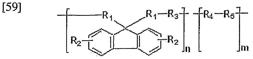
[46] Specifically, the antireflective hardmask composition comprises (a) at least one aromatic ring-containing polymer having a strong absorption in the short wavelength region (particularly, 248 nm or less), which is selected from the group consisting of polymers represented by formulae 1, 2 and 3:
Figure imgf000007_0001
[48] wherein each R1 is selected from
Figure imgf000007_0003
Figure imgf000007_0002
Figure imgf000007_0004
[50] (R is H or alkyl), eachR2 is selected from hydrogen (-H), hydroxy! (-OH), C1-Ci0 alkyl, C6-Ci0 aryl, allyl and halogen, R3 is selected from
Figure imgf000008_0001
[52] and 1 < n< 750;
Figure imgf000008_0002
54 wherein R is selected from
Figure imgf000008_0003
[56] (RisHorallcyl), R5 is selected from
[57]
Figure imgf000008_0004
[58] and 1 < n < 750; and
Figure imgf000008_0005
(3) [60] wherein RJ, R2, R3, R^, R5 and n are as defined in ϊbrmulae 1 and 1, 1 < m < 750, and
2 < m + n < 1,50O3 and
[61] (b) an organic solvent
[62] It is preferred that the aromatic ring-containing polymer (a) contains aromatic rings in the skeleton of the polymer. Since the aromatic rings absorb light of short wavelengths (248 nm or less) during lithography, the composition of the present invention can be used to form a hardmask layer that minimizes the reflectivity between a resist and an underlying layer, thus avoiding the formation of an additional antire- flective coating (ARQ.
[63] It is preferred that the aromatic ring-containing polymer has a number of reactive sites (i.e. hydroxyl (-OH) groups) distributed along the backbone chain of the polymer that reacts with a crosslinking component. At this time, the hydroxyl groups react with the adjacent hydroxyl groups or the terminal alkoxy (-OCH3) groups of the polymer ('self-crosslinkmg'). This self-crosslinking allows the antireflective hardmask composition of the present invention to be cured by baking without the use of an additional crosslinking component.
[64] The curing of the composition according to the present invention may be promoted by crosslinking with a crosslinking component other than the selfcrosslinking. That is, a number of reactive sites (particularly, hydroxyl (-OH) groups) distributed along the backbone of the polymer can be crosslinked with a crosslinking component,
[65] In addition, the antireflective hardmask composition of the present invention lias solution- and film-forming characteristics, which assist in the formation of a layer by a conventional spin-coating technique.
[66] AH the above requirements are met due to the presence of at least one aromatic ring- containing polymer selected from polymer selected from the group consisting of the polymers represented by ϊbrmulae 1, 2 and 3 in the hardmask composition of the present invention.
[67] The aromatic ring-containing polymer preferably has a weight average molecular weight of 1,000 to 30,000 Within this range, the aromatic ring-containing polymer is appropriately soluble in the solvent, rendering the hardmask composition suitable for coating.
[68] The aromatic ring-containing polymer (a) is preferably present in an amount of 1 to 30 parts by weight, based on 100 parts by weight of the organic solvent (b). The reason why the amount of the aromatic ring-containing polymer used is limited within the range defined above is that a desired coating thickness is not attained, Le. it is difficult to accurately regulate a coating thickness.
[69] There is no particular limitation on the kind of the organic solvent (b) so long as the aromatic ring-containing polymer (a) can be sufficiently dissolved in the organic solvent (b). As suitable organic solvents, there may be exemplified propylene glycol monomethyl ether acetate (PGMEA), propylene glycol monomethyl ether (PGME), cyclohexanone (Anone) and ethyl lactate (EL).
[Z)] The hardmask composition of the present invention may further comprise (c) a crosslinking component that is preferably capable of crosslinking the repeating units of the polymer upon heating. The hardmask composition of the present invention may further comprise (d) an acid or base catalyst that preferably serves to catalyze the crosslinking component (c). It is more preferred that the catalyst (d) be thermally activated.
[71] Any crosslinking component capable of reacting with the hydroxyl groups of the aromatic ring-containing polymer in a manner that can be catalyzed by the acid or base catalyst may be used without any particular limitation in the hardmask composition of the present invention.
[72] Specific examples of suitable crosslinking components for use in the antireflective hardmask composition of the present invention include: etherified amino resins, methylated melamine resins (e.g,, N-methoxymethyl-melamine resins), butylated melamine resins (e.g., N-butoxymethyl-melamine resins), methylated and butylated urea resins (e.g., Cymel U-65 Resin and UFR 80 Resin), glycoluril derivatives (e.g., Powderlink 1174), and 2,6-bis(hydroxymethyl)-/?-cresol.
[73] The Powderlink 1174 is a compound of Ramula 4:
Figure imgf000010_0001
[75] As the crosslinking component, there may be used the bisepoxy compound of formula 5:
[77] Exemplary acid catalysts include organic acids, e.g,, p-toluenesulfonic acid monohydrate. In view of storage stability, a thermal acid generator (TAG) may be used as the acid catalyst. TAG is a compound that generates an acid upon thermal treatment. Examples of preferred TAGs include pyridinium p-toluenesύlfonate, 2,4,4 ,6-tetrabromocyclohexadienol, benzoin tosylate, 2-nitrobenzyl tosylate, and alkyl esters of organic sulfonic acids.
[78] The base catalyst may be selected from ammonium hydroxides represented by NH4
OH or NR 4OH (R = alkyl).
[79] Other radiation-sensitive acid catalysts known in the field of resists can also be used so long as they are compatible with the other components of the antireflective composition.
[80] In the hardmask composition of the present invention, the aromatic ring-containing polymer (a) is preferably present in an amount of 1 to 2C% by weight and more preferably 3 to 10% by weight, the organic solvent (b) is preferably present in an amount of 75 to 98.8% by weight, the crosslinking component (c) is preferably present in an amount of Ql to 5% by weight and more preferably Ql to 3% by weight, and the acid or base catalyst (d) is preferably present in an amount of QOOl to Q05% by weight and more preferably QOOl to QQ3% by weight.
[81] When the content of the aromatic ring-containing polymer (a) is outside the range defined above, a desired coating thickness is not attained, Le. it is difficult to accurately regulate a coating thickness.
[82] When th& content of the organic solvent is outside the range defined above, a desired coating thickness is not attained, Le. it is difficult to accurately regulate a coating thickness.
[83] When the content of the crosslinking component is les s than Q 1 % by weight, crosslinking properties may be not exhibited. Meanwhile, when the content of the crosslinking component is greater than 5% by weight, deformation of a pattern profile may be caused and redeposition contamination may occur due to volatile components evolved upon baking.
[84] When the content of the acid or base catalyst is less than QOO 1% by weight, crosslinking properties may be not exhibited. Meanwhile, when the content of the acid or base catalyst exceeds Q05% by weight, the storage stability of the composition may be adversely affected.
[85] The hardmask composition of the present invention may further comprise at least one additive, such as a surfactant.
[86] The present invention also provides a method for patterning an underlying material layer on a substrate by using the hardmask composition. [87] Specifically, the method of the present invention comprises the steps of (a) providing a material layer on a substrate, (b) forming an antireflective hardmask layer using the composition on the material layer, (c) forming a radiation-sensitive imaging layer on the antireflective hardmask layer, (d) patternwise exposing the radiation-sensitive imaging layer to radiation to form a pattern of radiation-exposed regions in the imaging layer, (e) selectively removing portions of the radiation-sensitive imaging layer and the hardmask layer to expose portions of the material layer, and (f) etching the exposed portions of the material layer to pattern the material layer.
[88] The method may further comprise the step of forming a silicon-containing hardmask layer prior to step (c). The method may further comprise the step of forming a bottom antireflective hardmask layer (BARQ on the silicon-containing hardmask layer prior to step (c).
[89] Specifically, the method of the present invention can be carried out in accordance with the following procedure. Erst, a material ( e.g., aluminum or silicon nitride (SN)) to be patterned is applied to a silicon substrate by any technique known in the art, The material may be an, electrically conductive, semi-conductive, magnetic or insulating material. Thereafter, the hardmask composition of the present invention is spin-coated to a thickness of 500 to 8,000 and baked at 100-30CFC for 10 seconds to 10 minutes to form a hardmask layer. Thereafter, a silicon-containing hardmask composition may be spin-coated to a thickness of 500 to 4,000 on the hardmask layer and baked at 100-3 OCPC for 10 seconds to 10 minutes to form a silicon-containing hardmask layer. If needed, a bottom antireflective coating (BARQ may be formed on the silicon- containing hardmask layer.
[90] A radiation- sensitive image layer is formed on the hardmask layer. Light exposure and development are performed to form a pattern on the imaging layer. Dry etching is performed using a gas mixture, such as CHP3/CF4, through recessed portions of the patterned imaging layer to transfer the pattern to the silicon-containing hardmask layer. After the dry etching, a gas mixture, such as BC13/C12, is used to etch the exposed portions of the hardmask layer through the patterned silicon hardmask layer as a mask. As a result, the hardmask layer is patterned.
[91] Dry etching is performed using a gas mixture, such as CHF3/CF4, to pattern the material layer on the substrate. Ashing may be performed to remove the remaining material, leaving the patterned material layer only, for example, the removal of the remaining material can be accomplished using oxygen plasma. The method of the present invention can be applied to the fabrication of a semiconductor integrated circuit device.
[92] Hereinafter, the present invention will be explained in more detail with reference to the following examples. However, these examples are given for the purpose of illustration only and are not intended to limit the scope of the invention.
[93]
Mode for the Invention
[94] [Synthesis Example 1] [95] (Synthesis of terpolymer of 9,9'-bishydroxynaphthylfluorene, 1-naphthol and 9, 10-bismethoxymethylanthracene)
[96] 45Q5g (1.0 mol) of 9,9'-bishydroxynaρhthylfluorene, 144.2g (1.0 mol) of 1-naphthol, 3.1g (Q02 mol) of diethyl sulfate and 350g of propylene glycol monomethyl ether were completely dissolved with stirring in a 3 L three-neck flask equipped with a mechanical agitator and a condenser while maintaining the temperature of the reactor at IGCC. 10 minutes afterthe dissolution, 532.7g of (2.0 mol) of 9,10-bismefhoxymethylanthracene was dropped into the solution, and then the resulting mixture was allowed to react at 12UC for 15 hours. To the reaction mixture was added 2.98g (Q02 mol) of triethanolamine as a neutralizing agent to quench the reaction. After completion of the reaction, a water/methanol mixture was used to remove the acid from the reaction mixture, and methanol was used to remove low- molecular weight compounds containing the oligomers and monomers, yielding the polymer represented by Ibrmula 6 (M w = 10,000, polydspersity = 2.0, n =≤ 10, m = 9).
[98] [99] [Synthesis Example 2] [100] (Synthesis of terpolymer of 9,9'-bishydroxynaphthylfluorene, 1-hydroxypyrene and 1 ,4-bismethoxymethylbenzene)
[101] The procedure of Synthesis Example 1 was repeated except that 218.3g (1 mol) of 1-hydroxypyrene was added instead of 144.2g of 1-naphthol and 332.9g (2 mol) of 1,4-bismethoxymethylbenzene was added instead of 532.7g of (2.0 mol) of 9,10-bismethoxymethylanthracene, yielding the copolymer of Ibrmula 7:
Figure imgf000014_0001
[IGB] The molecular weight and the polydispersity of the copolymer were measured by gel permeation chromatography (GPQ in tetrahydrofuran. As a result, the copolymer was found to have a molecular weight of 11,000 (n = 10, m = 11) and a polydispersity of 2.2.
[104] [105] [Synthesis Example 3] [106] (Synthesis of terpolymer of 9,9'-bishydroxynaphthylfluorene, phenol and formaldehyde)
[107] The procedure of Synthesis Example 1 was repeated except that 94.1g (1,0 mol) of phenol was added instead of 144.2g of 1-naphthol and ffllg (2 mol) of formaldehyde was ailed instead of 532.7g of (2.0 mol) of 9, 10-bismethoxymethylanthracene, yielding the copolymer of Formula 8:
Figure imgf000014_0002
[109] The molecular weight and the polydispersity of the copolymer were measured by gel permeation chromatography (GPQ in tetrahydrofuran. As a result, the copolymer was found to have a.molecular weight of 10,000 (n = 8, m = 8) and a polydispersity of 1.8,
[HO] [111] [Synthesis Example 4] [112] (Synthesis of copolymer of 9,9'-bishydroxynaphthylfluorene and 1,4-bismethoxymethylbenzene and copolymer of 9,9'-bishydroxyphenylfluorene and 1,4-bismethoxymethylbenzene, and preparation of blend of the copolymers)
[113] 45Q5g (1.0 mol) of 9,9'-bishydroxynaphthylfluorene, 3.1g (Q02 mol) of diethyl sulfate and 25Og of propylene glycol "monomethyl ether were completely dissolved with stirring in a 2 L three-neck flask equipped with a mechanical agitator and a condenser while maintaining the temperature of the reactor at 1001C. 10 minutes after the dissolution, 166.4g (1.0 mol) of 1,4-bismethoxymethylbenzene was dropped into the solution, and then the resulting mixture was allowed to react at 12CfC for 24 hours. To the reaction mixture was added 2.98g (Q02 mol) of triethanolamine as a neutralizing agent to quench the reaction. After completion of the reaction, a water/ methanol mixture was used to remove the acid from the reaction mixture, and methanol was used to remove low-molecular weight compounds containing the oligomers and monomers, yielding the polymer represented by Ibrmula 9 (M w = 10,000, polydispersity = 2.3, n = 20).
Figure imgf000015_0001
[115] 393.5g (1.0 mol) of 9,9'-bishydroxyρhenylfluorene, 3.1g (002 mol) of diethyl sulfate and 25Og of propylene glycol monomethyl ether were completely dissolved with stirring in a 2 L three-neck flask equipped with a mechanical agitator and a condenser while maintaining the temperature of the reactor at 1000C. 10 minutes after the dissolution, 166.4g of (1.0 mol) of 1,4-bismethoxymethylbenzene was dropped into the solution, and then the resulting mixture was allowed to react at 12CPCfor 15 hours, To the reaction mixture was added 2,98g (Q02 mol) of triethanolamine as a neutralizing agent to quench the reaction. After completion of the reaction, a water/methanol mixture was used to remove the acid from the reaction mixture, and methanol was used to remove low-molecular weight compounds containing the oligomers and monomers, yielding the polymer represented by Iormula 10 (M w = 10,000, polydispersity = 1.9, n = 22).
Figure imgf000015_0002
[117] [118] The polymers of R>rmulae 9 and 10 were mixed together in a ratio of 9:1 to prepare a blend,
[119] [120] [Examples 1 to 4] [121] Q8g of each of the polymers prepared in Synthesis Examples 1 to 4, Q2g of Powderlink 1174 (Ebrmula 4) as a crosslinker and 2 mg of pyridnium p - toluenesulfonate were dissolved in 9g of propylene glycol mononiethyl ether acetate (PGMEA), and filtered to prepare a sample solution.
[122] Each of the sample solutions prepared in Examples 1 to 4 was spin-coated on a silicon wafer and baked at 2001C for 60 seconds to form a 4,000A-thick film.
[123] The refractive index (n) and extinction coefficient (k) of the films were measured using an ellipsometer (J. A. Woollam). The results are shown in Table 1.
[124] The data of Table 1 show that the films are suitable for use as antireflective firms at 193nm (ArF) and 248 nm (KrF).
[125] TABLE 1
[126]
Optical properties Cl 93 nrrύ Optical properties ("248 nmi
Sarnple used in the formation of film Refractive Extinction Refractive Extinction index (n) coefficient (k) index (n) coefficient (k)
Example 1 1.47 0.65 1.90 0.20
Example 2 1.43 0,30 2.11 0.28
Example 3 1.44 0.71 1.80 0.06
Example 4 1.43 0.69 1.83 0.07
[127] [Examples 5 to 8]
[128] Each of the sample solutions prepared in Examples 1 to 4 was spin-coated on a silicon wafer covered with silicon nitride and baked at 2001C for 60 seconds to form a 4,000 A-thick film.
[129] A silicon antireflective coating (ARQ was formed on the film and baked at 240C for 60 seconds. Thereafter, an ArF photoresist (PR) was coated to a thickness of 1,XK) on the silicon ARC, baked at 1 ICPC for 60 seconds, exposed to light using an ArF exposure system (ASML, XT: 1400, NA Q93), and developed with an aqueous solution of TMAH (2.38 wt%) to form a 63-nm line and space pattern. The patterns were observed using a field emission scanning electron microscope (FE-SEM). The patterns were measured for exposure latitude (EL) margin as a function of exposure energy and depth of focus (DoF) margin as a function of the distance from a light source. The results are recorded in Table 2.
[130] TABLE 2 T/KR2007/007059
16
[131]
Pattern properties
Sample used in the formation of film EL margin DoF margin (μm) Profile (Δ mJ/exρosure energy mJ)
Example 5 4 0.25 Cubic
Example 6 4 0.25 Cubic
Example ? 4 0.25 Cubic
Example S 4 0.25 Cubic
[132] [Examples 9 to 12]
[133] Each of the silicon ARCs of the patterned specimens (Examples 5 to 8) was dry- etched using a gas mixture of CHF3/CF4 through a photoresist (PR) as a mask. The hardmaslc was dry-etched using a gas mixture OfO2ZN2 through the silicon ARC as a mask. Thereafter, the silicon nitrϋe was dry-etched using a gas mixture OfCHF3ZCF4 through the hardmask as a mask. O2 ashing and wet stripping were performed on the remaining portions of the hardmask and the organic material.
[134] Immediately after etching of the hardmask and the silicon nitride, the cross sections of the specimens were observed using an FE-SEM. The results are listed in Table 3.
[135] The etched patterns all showed good profiles without being bowed or tapered. The reason for good etching of the silicon nitride Is believed to be because the hardmasks were sufficiently resistant to the etching gas.
[136] TABLE 3
[137]
Sample used in the Pattern shape after Pattern shape after formation of film etching of hardmask etching of silicon nitride
Example 9 Vertical (Anisotropic) Vertical (Anisotropic)
Example 10 "Vertical (Anisotropic) Vertical (Anisotropic)
Example U Vertical (Anisotropic) Vertical (Anisotropic)
Example 12 Vertical (Anisotropic) Vertical (Anisotropic)
[138] As apparent from the above description, the antiretlective hardmask composition of the present invention can be used to form a film having a refractive index and an ab- sorbance suitable for use as an antireflective film in the deep UV (DUV) (e.g., ArF (193 nm) and KrF (248 nm)). Therefore, the antireflective hardmask composition of the present invention exhibits -very high etch selectivity for lithography. In addition, since the antireflective hardmask composition of the present invention is sufficiently resistant to multiple etching, it can be used to form a hardmask having a very good etch profile. Therefore, a good image can be transferred to an underlying layer. Fur- thermore, since the antirefiective hardmask composition of the present invention can minimize the reflectivity between a resist and an underlying layer, it can be used to provide a lithographic structure that has better results in terms of pattern profile and margins.
[139]
Industrial Applicability
[140] Accordingly, the composition of the present invention and the resulting lithographic structure can be used in the fabrication and design of integrated circuit devices. R>r example, the composition of the present invention can be used in the formation of patterned material layer structures, such as metal wirings, holes for contacts and biases, insulating sections (e.g., damascene trenches (DTs) and shallow trench isolation (STT)), and trenches for capacitor structures. It should be appreciated that the present invention is not restricted to any particular lithographic techniques and device structures.
[141]

Claims

Claims
[1] An antireflective hardmask composition comprising
(a) at least one aromatic ring-containing polymer selected from the group consisting of polymers represented by Rrmulae 1, 2 and 3:
Figure imgf000019_0001
wherein ea
Figure imgf000019_0003
Figure imgf000019_0002
Figure imgf000019_0004
(R is H or alkyl), each R2 is selected from hydrogen (-H), hydroxyl (-OH), C1-Ci0 alkyl, C6-Ci0 ∞yh allyl and halogen, R3 is selected from
Figure imgf000019_0005
and 1 ≤ n < 750;
4-R4-R5H- I In (2) wherein R4 is selected from
Figure imgf000020_0001
(R is H or alkyl), R5 is selected from
Figure imgf000020_0002
and 1 < n < 750; and
Figure imgf000020_0003
wherein R1, R2, R3, R4, Rs and n are as defined in Ibrmulae 1 and 2, 1 <■ m < 750, and2 < m + n < 1,500, and
(b) an organic solvent,
[2] The composition according to claim 1, further comprising (c) a crosslinking component.
[3] The composition according to claim 2, further comprising (d) an acid or base catalyst.
[4] The composition according to claim 3, wherein the composition comprises 1 to
20% by weight of the aromatic ring-containing polymer (a), 75 to 98.8% by weight of the organic solvent Qo), Ql to 5% by weight of the crosslinking component (c), and QOOl to Q05% by weight of the acid or base catalyst (d).
[5] The composition according to claim 1, wherein the aromatic ring-containing polymer has a weight average molecular weight of 1,000 to 30.,00Q
[6] The composition according to claim 1 , further comprising a surfactant.
[7J The composition according to claim 2, wherein the cros slinking component is selected from the group consisting of melamine resins, amino resins, glycoluril compounds, and bisepoxy compounds.
[8] The composition according to claim 33 wherein the acid catalyst is selected from the group consisting of p-toluenesulfonic acid monohydrate, pyridinium p - toluenesulfonate, 2,4,4,6-tetrabromocyclohexadienone, benzoin tosylate, 2-nitrobenzyl tosylate, and alkyl esters of organic sulfonic acids.
[9] The composition according to claim 3, wherein the base catalyst is selected from ammonium hydroxides represented by NH4OH or JSR+OH (R = alkyl).
[10] A method for patterning a material on a substrate, the method comprisingthe steps of (a) providing a material layer on a substrate, (b) forming an antire- flective hardmask layer using the composition according to claim 1 on the material layer, (c) forming a radiation-sensitive imaging layer on the antirefleetive hardmask layer, (d) patternwise exposing the radiation-sensitive imaging layer to radiation to form a pattern of radiation-exposed regions in the imaging layer, (e) selectively removing portions of the radiation-sensitive imaging layer and the antirefleetive hardmask layer to expose portions of the material layer, and (f) etching the exposed portions of the material layer to pattern the material layer.
[11] The method according to claim 10, further comprising the step of forming a silicon-containing hardmask layer prior to step (c).
[12] The method according to claim 11, further comprising the step of forming a bottom antirefleetive coating (BARQ on the silicon-containing hardmask layer prior to step (c).
PCT/KR2007/007059 2007-06-05 2007-12-31 Hardmask composition having antireflective properties and method of patterning material on substrate using the same Ceased WO2008150058A1 (en)

Priority Applications (2)

Application Number Priority Date Filing Date Title
CN200780053206A CN101681096A (en) 2007-06-05 2007-12-31 Hardmask composition having antireflective properties and method of patterning material on substrate using the same
JP2010511100A JP2010529499A (en) 2007-06-05 2007-12-31 Anti-reflective hard mask composition and method for patterning material on a substrate using the same

Applications Claiming Priority (2)

Application Number Priority Date Filing Date Title
KR1020070055243A KR100908601B1 (en) 2007-06-05 2007-06-05 Anti-reflective hard mask composition and patterning method of substrate material using same
KR10-2007-0055243 2007-06-05

Publications (1)

Publication Number Publication Date
WO2008150058A1 true WO2008150058A1 (en) 2008-12-11

Family

ID=40093842

Family Applications (1)

Application Number Title Priority Date Filing Date
PCT/KR2007/007059 Ceased WO2008150058A1 (en) 2007-06-05 2007-12-31 Hardmask composition having antireflective properties and method of patterning material on substrate using the same

Country Status (6)

Country Link
US (2) US7981594B2 (en)
JP (1) JP2010529499A (en)
KR (1) KR100908601B1 (en)
CN (1) CN101681096A (en)
TW (1) TWI380133B (en)
WO (1) WO2008150058A1 (en)

Cited By (6)

* Cited by examiner, † Cited by third party
Publication number Priority date Publication date Assignee Title
US20100021830A1 (en) * 2007-04-02 2010-01-28 Min Soo Kim Aromatic ring-containing polymer, polymer mixture, antireflective hardmask composition, and associated methods
JP2010122656A (en) * 2008-10-20 2010-06-03 Shin-Etsu Chemical Co Ltd Method for forming resist underlayer film, patterning process using the same, and resist underlayer film material
CN102060980A (en) * 2009-11-13 2011-05-18 第一毛织株式会社 Resist underlayer polymer, resist underlayer composition including the same, and method of patterning using the same
CN102566282A (en) * 2010-12-17 2012-07-11 第一毛织株式会社 Hardmask composition, method of forming a pattern, and semiconductor integrated circuit device including the pattern
JP2014515121A (en) * 2011-03-30 2014-06-26 エイゼット・エレクトロニック・マテリアルズ・ユーエスエイ・コーポレイション Anti-reflective coating composition and method thereof
US10394124B2 (en) 2014-11-04 2019-08-27 Nissan Chemical Industries, Ltd. Resist underlayer film-forming composition containing polymer having arylene group

Families Citing this family (78)

* Cited by examiner, † Cited by third party
Publication number Priority date Publication date Assignee Title
US20080292987A1 (en) * 2007-05-22 2008-11-27 Francis Houlihan Antireflective Coating Composition Comprising Fused Aromatic Rings
US8017296B2 (en) 2007-05-22 2011-09-13 Az Electronic Materials Usa Corp. Antireflective coating composition comprising fused aromatic rings
KR100908601B1 (en) * 2007-06-05 2009-07-21 제일모직주식회사 Anti-reflective hard mask composition and patterning method of substrate material using same
US7989144B2 (en) * 2008-04-01 2011-08-02 Az Electronic Materials Usa Corp Antireflective coating composition
US7932018B2 (en) * 2008-05-06 2011-04-26 Az Electronic Materials Usa Corp. Antireflective coating composition
US20100119979A1 (en) * 2008-11-13 2010-05-13 Rahman M Dalil Antireflective Coating Composition Comprising Fused Aromatic Rings
US20100119980A1 (en) * 2008-11-13 2010-05-13 Rahman M Dalil Antireflective Coating Composition Comprising Fused Aromatic Rings
KR101766796B1 (en) * 2008-11-27 2017-08-09 닛산 가가쿠 고교 가부시키 가이샤 Composition for forming resist underlayer film with reduced outgassing
US20100151392A1 (en) * 2008-12-11 2010-06-17 Rahman M Dalil Antireflective coating compositions
WO2010127941A1 (en) 2009-05-07 2010-11-11 Basf Se Resist stripping compositions and methods for manufacturing electrical devices
EP2427803B1 (en) 2009-05-07 2017-12-13 Basf Se Methods for manufacturing electrical devices using resist stripping compositions
JP5836932B2 (en) 2009-05-07 2015-12-24 ビーエーエスエフ ソシエタス・ヨーロピアBasf Se Resist stripping composition and method for manufacturing an electrical device
US20100316949A1 (en) * 2009-06-10 2010-12-16 Rahman M Dalil Spin On Organic Antireflective Coating Composition Comprising Polymer with Fused Aromatic Rings
US8486609B2 (en) * 2009-12-23 2013-07-16 Az Electronic Materials Usa Corp. Antireflective coating composition and process thereof
KR101400182B1 (en) * 2009-12-31 2014-05-27 제일모직 주식회사 Photoresist underlayer composition and method of manufacturing semiconductor device by using the same
KR101344794B1 (en) 2009-12-31 2014-01-16 제일모직주식회사 Aromatic ring-containing polymer for resist underlayer and resist underlayer composition including same
JP5068828B2 (en) * 2010-01-19 2012-11-07 信越化学工業株式会社 Resist underlayer film forming composition, resist underlayer film forming method, and pattern forming method
KR101400183B1 (en) * 2010-07-06 2014-05-30 제일모직 주식회사 Aromatic ring-containing compound for resist underlayer, resist underlayer composition including same, and method of patterning device using same
JP5556773B2 (en) * 2010-09-10 2014-07-23 信越化学工業株式会社 Naphthalene derivative and method for producing the same, resist underlayer film material, resist underlayer film forming method and pattern forming method
KR101432605B1 (en) * 2010-12-16 2014-08-21 제일모직주식회사 Hardmask composition and method of forming patterns and semiconductor integrated circuit device including the patterns
JP5598489B2 (en) * 2011-03-28 2014-10-01 信越化学工業株式会社 Biphenyl derivative, resist underlayer film material, resist underlayer film forming method and pattern forming method
WO2013100375A1 (en) * 2011-12-30 2013-07-04 제일모직 주식회사 Composition for forming a hardmask, method for forming a pattern using same, and semiconductor integrated circuit device comprising the pattern
US9725389B2 (en) 2011-12-30 2017-08-08 Cheil Industries, Inc. Monomer for a hardmask composition, hardmask composition comprising the monomer, and method for forming a pattern using the hardmask composition
KR101413071B1 (en) * 2011-12-30 2014-07-02 제일모직 주식회사 Monomer for hardmask composition and hardmask composition including the monomer and method of forming patterns using the hardmask composition
KR101497132B1 (en) * 2011-12-30 2015-03-02 제일모직 주식회사 Monomer for hardmask composition and hardmask composition including the monomer and method of forming patterns using the hardmask composition
KR101531610B1 (en) 2011-12-30 2015-06-24 제일모직주식회사 Composition for hardmask, method of forming patterns using the same, and semiconductor integrated circuit device including the patterns
KR101413069B1 (en) 2011-12-30 2014-07-02 제일모직 주식회사 Monomer for hardmask composition and hardmask composition including the monomer and method of forming patterns using the hardmask composition
CN104380194B (en) * 2012-04-16 2019-05-31 布鲁尔科技公司 Silicon hardmask layers for guided self-assembly
JP5894106B2 (en) 2012-06-18 2016-03-23 信越化学工業株式会社 Compound for forming resist underlayer film, resist underlayer film material using the same, resist underlayer film forming method, pattern forming method
US8906592B2 (en) 2012-08-01 2014-12-09 Az Electronic Materials (Luxembourg) S.A.R.L. Antireflective coating composition and process thereof
KR101912677B1 (en) * 2012-08-10 2018-10-29 닛산 가가쿠 가부시키가이샤 Composition for forming resist underlayer film
KR101566533B1 (en) * 2012-10-24 2015-11-05 제일모직 주식회사 Hardmask composition and method of forming patterns using the hardmask composition
KR102099712B1 (en) 2013-01-15 2020-04-10 삼성전자주식회사 Method of forming a pattern and method of manufacturing a semiconductor device using the same
KR101682021B1 (en) * 2013-03-20 2016-12-02 제일모직 주식회사 Hardmask composition and method of forming patterns using the hardmask composition
KR102066229B1 (en) 2013-03-26 2020-01-15 주식회사 동진쎄미켐 Under-layer composition of resist and method for forming pattern using the the same
CN105143390B (en) 2013-04-17 2019-08-13 三星Sdi株式会社 Organic membrane chemical mechanical polishing slurry composition and polishing method using same
US9152051B2 (en) * 2013-06-13 2015-10-06 Az Electronics Materials (Luxembourg) S.A.R.L. Antireflective coating composition and process thereof
KR101696197B1 (en) * 2013-06-27 2017-01-13 제일모직 주식회사 Hardmask composition, method of forming patterns using the hardmask composition and semiconductor integrated circuit device including the patterns including the patterns
CN104253024B (en) * 2013-06-27 2017-07-28 第一毛织株式会社 Hard mask compositions, the method using its formation pattern and the conductor integrated circuit device including the pattern
TWI643902B (en) * 2013-07-31 2018-12-11 Skc股份有限公司 Composition having high heat-and chemical-resistance and method for preparing protective thin film using same
KR101521618B1 (en) * 2013-12-30 2015-05-19 에스케이씨 주식회사 Composition for the formation of a protective thin film having high heat resistance and chemical resistance, and method for preparing a protective thin film using same
KR101582462B1 (en) * 2013-08-23 2016-01-06 (주)디엔에프 new polymer and compositions containing it
TWI542614B (en) * 2013-12-12 2016-07-21 羅門哈斯電子材料有限公司 Lower layer of aromatic resin
US9761449B2 (en) 2013-12-30 2017-09-12 Taiwan Semiconductor Manufacturing Company, Ltd. Gap filling materials and methods
KR20150079199A (en) * 2013-12-31 2015-07-08 제일모직주식회사 Hardmask composition, method of forming patterns using the hardmask composition and semiconductor integrated circuit device including the patterns
US10294183B2 (en) * 2014-03-13 2019-05-21 Mitsubishi Gas Chemical Company, Inc. Compound, resin, material for forming underlayer film for lithography, underlayer film for lithography, pattern forming method, and method for purifying the compound or resin
US9362120B2 (en) 2014-03-31 2016-06-07 Taiwan Semiconductor Manufacturing Company, Ltd. Lithography process and composition with de-crosslinkable crosslink material
US9274426B2 (en) * 2014-04-29 2016-03-01 Az Electronic Materials (Luxembourg) S.A.R.L. Antireflective coating compositions and processes thereof
KR101754901B1 (en) 2014-05-16 2017-07-06 제일모직 주식회사 Hardmask composition and method of forming patterns using the hardmask composition
KR101747229B1 (en) 2014-07-15 2017-06-14 삼성에스디아이 주식회사 Hardmask composition and method of forming patterns using the hardmask composition
KR102295525B1 (en) 2015-01-16 2021-08-30 삼성전자 주식회사 Hard mask composition for spin coating
US9908990B2 (en) 2015-04-17 2018-03-06 Samsung Sdi Co., Ltd. Organic layer composition, organic layer, and method of forming patterns
KR101814671B1 (en) * 2015-06-02 2018-01-04 삼성에스디아이 주식회사 Organic layer composition, organic layer, and method of forming patterns
KR102520797B1 (en) 2015-10-15 2023-04-12 삼성전자주식회사 Reflective Photo Mask and Manufacturing Method thereof
KR101926023B1 (en) * 2015-10-23 2018-12-06 삼성에스디아이 주식회사 Method of producimg layer structure, and method of forming patterns
KR101852460B1 (en) 2015-12-16 2018-04-26 삼성에스디아이 주식회사 Polymer, organic layer composition, and method of forming patterns
KR101770749B1 (en) 2016-01-11 2017-08-23 최상준 A Composition of Anti-Reflective Hardmask
KR102702993B1 (en) 2016-11-25 2024-09-04 삼성전자주식회사 Method of forming patterns for semiconductor device
JP7008075B2 (en) * 2016-12-21 2022-01-25 メルク パテント ゲゼルシャフト ミット ベシュレンクテル ハフツング Composition of spin-on material containing metal oxide nanoparticles and organic polymer
KR102383692B1 (en) * 2017-06-30 2022-04-05 동우 화인켐 주식회사 Composition for hard mask
KR102351175B1 (en) * 2017-07-25 2022-01-14 에스케이이노베이션 주식회사 Novel polymer for preparing resist underlayer film, resist underlayer film composition containing the polymer and method for manufacturing semiconductor device using the composition
KR102118874B1 (en) * 2018-05-25 2020-06-04 (주)코이즈 Organic hard mask composition for anti-reflection and method of forming patterns using the composition
KR102244470B1 (en) 2018-07-18 2021-04-23 삼성에스디아이 주식회사 Polymer, organic layer composition and method of forming patterns
KR102197249B1 (en) 2018-11-30 2020-12-31 주식회사 에이치앤에스 reflective protective hard coating composition
KR102109919B1 (en) 2019-01-18 2020-05-12 주식회사 오라스 A composition of anti-reflective hardmask
KR102240213B1 (en) * 2019-04-09 2021-04-14 영창케미칼 주식회사 Spin on carbon hardmask compositions with characteristics of high thickness and patterning method by using the same
KR102448568B1 (en) 2020-01-17 2022-09-27 삼성에스디아이 주식회사 Resist underlayer composition, and method of forming patterns using the composition
KR102252677B1 (en) 2020-09-21 2021-05-14 최상준 A composition of anti-reflective hardmask
KR102246532B1 (en) 2020-10-28 2021-04-29 최상준 A composition of anti-reflective hardmask
KR102350590B1 (en) * 2021-05-17 2022-01-12 영창케미칼 주식회사 Spin on carbon hardmask compositions with low evaporation loss and patterning method by using the same
KR102623450B1 (en) 2021-09-07 2024-01-10 주식회사 켐폴 A composition of anti-reflective hardmask
KR102907251B1 (en) * 2022-05-03 2026-01-02 (주)휴넷플러스 Organic polymer, semiconductor hard mask composition comprising the same, and patterning method using the same
KR102757070B1 (en) 2022-12-27 2025-01-24 주식회사 휴인터내셔널 A composition of anti-reflective hardmask
KR102868662B1 (en) 2023-01-04 2025-10-13 주식회사 켐폴 A composition of anti-reflective hardmask
KR20250067604A (en) 2023-11-08 2025-05-15 주식회사 제이앤씨머트리얼즈 A composition of anti-reflective hardmask
KR20250067614A (en) 2023-11-08 2025-05-15 주식회사 제이앤씨머트리얼즈 A composition of anti-reflective hardmask
KR102894059B1 (en) 2024-03-20 2025-12-02 주식회사 켐폴 New aromatic condensation polymer and resist underlayer composition
KR102882891B1 (en) 2025-02-21 2025-11-07 주식회사 켐폴 Polymer for antireflection and hard mask composition comprising the same

Citations (5)

* Cited by examiner, † Cited by third party
Publication number Priority date Publication date Assignee Title
US20060251990A1 (en) * 2005-05-09 2006-11-09 Uh Dong S Antireflective hardmask composition and methods for using same
KR20060132070A (en) * 2005-06-17 2006-12-21 제일모직주식회사 Antireflective hardmask composition and method for forming patterned material shape on substrate using same
US20070003863A1 (en) * 2005-06-17 2007-01-04 Uh Dong S Antireflective hardmask composition and methods for using same
KR20070002591A (en) * 2005-06-30 2007-01-05 주식회사 하이닉스반도체 Composition for hard mask and pattern formation method using same
KR100713231B1 (en) * 2005-12-26 2007-05-02 제일모직주식회사 Hard mask composition for resist underlayer film and manufacturing method of semiconductor integrated circuit device using same

Family Cites Families (13)

* Cited by examiner, † Cited by third party
Publication number Priority date Publication date Assignee Title
WO2002046507A2 (en) * 2000-12-04 2002-06-13 Ciba Specialty Chemicals Holding Inc. Onium salts and the use therof as latent acids
US7303855B2 (en) * 2003-10-03 2007-12-04 Shin-Etsu Chemical Co., Ltd. Photoresist undercoat-forming material and patterning process
KR100671115B1 (en) * 2005-05-09 2007-01-17 제일모직주식회사 Hard mask composition having antireflection
KR100655064B1 (en) * 2005-05-27 2006-12-06 제일모직주식회사 Hard mask composition having antireflection
KR100665758B1 (en) * 2005-09-15 2007-01-09 제일모직주식회사 Hard mask composition having antireflection
KR100697979B1 (en) * 2005-09-26 2007-03-23 제일모직주식회사 Antireflective Hardmask Composition
JP4421566B2 (en) 2005-12-26 2010-02-24 チェイル インダストリーズ インコーポレイテッド Hard mask composition for photoresist underlayer film and method of manufacturing semiconductor integrated circuit device using the same
WO2007139268A1 (en) * 2006-05-30 2007-12-06 Cheil Industries Inc. Antireflective hardmask composition
KR100816735B1 (en) * 2006-12-20 2008-03-25 제일모직주식회사 Anti-reflective hard mask composition, patterned material shape fabrication method and semiconductor integrated circuit device using same
KR100896451B1 (en) * 2006-12-30 2009-05-14 제일모직주식회사 Highly etch resistant anti-reflective hard mask composition with improved carbon content, method of manufacturing patterned material shape using same
JP5118191B2 (en) 2007-04-02 2013-01-16 チェイル インダストリーズ インコーポレイテッド Anti-reflective hard mask composition and material pattern forming method using the same
KR100908601B1 (en) * 2007-06-05 2009-07-21 제일모직주식회사 Anti-reflective hard mask composition and patterning method of substrate material using same
KR100930673B1 (en) * 2007-12-24 2009-12-09 제일모직주식회사 Method for patterning materials using antireflective hard mask compositions

Patent Citations (5)

* Cited by examiner, † Cited by third party
Publication number Priority date Publication date Assignee Title
US20060251990A1 (en) * 2005-05-09 2006-11-09 Uh Dong S Antireflective hardmask composition and methods for using same
KR20060132070A (en) * 2005-06-17 2006-12-21 제일모직주식회사 Antireflective hardmask composition and method for forming patterned material shape on substrate using same
US20070003863A1 (en) * 2005-06-17 2007-01-04 Uh Dong S Antireflective hardmask composition and methods for using same
KR20070002591A (en) * 2005-06-30 2007-01-05 주식회사 하이닉스반도체 Composition for hard mask and pattern formation method using same
KR100713231B1 (en) * 2005-12-26 2007-05-02 제일모직주식회사 Hard mask composition for resist underlayer film and manufacturing method of semiconductor integrated circuit device using same

Cited By (11)

* Cited by examiner, † Cited by third party
Publication number Priority date Publication date Assignee Title
US20100021830A1 (en) * 2007-04-02 2010-01-28 Min Soo Kim Aromatic ring-containing polymer, polymer mixture, antireflective hardmask composition, and associated methods
US8420289B2 (en) * 2007-04-02 2013-04-16 Cheil Industries, Inc. Aromatic ring-containing polymer, polymer mixture, antireflective hardmask composition, and associated methods
JP2010122656A (en) * 2008-10-20 2010-06-03 Shin-Etsu Chemical Co Ltd Method for forming resist underlayer film, patterning process using the same, and resist underlayer film material
US8450048B2 (en) 2008-10-20 2013-05-28 Shin-Etsu Chemical Co., Ltd. Method for forming resist underlayer film, patterning process using the same, and composition for the resist underlayer film
US8652757B2 (en) 2008-10-20 2014-02-18 Shin-Etsu Chemical Co., Ltd. Method for forming resist underlayer film, patterning process using the same, and composition for the resist underlayer film
CN102060980A (en) * 2009-11-13 2011-05-18 第一毛织株式会社 Resist underlayer polymer, resist underlayer composition including the same, and method of patterning using the same
US9116429B2 (en) 2009-11-13 2015-08-25 Cheil Industries, Inc. Resist underlayer polymer, resist underlayer composition including the same, and method of patterning using the same
CN102566282A (en) * 2010-12-17 2012-07-11 第一毛织株式会社 Hardmask composition, method of forming a pattern, and semiconductor integrated circuit device including the pattern
US8741539B2 (en) 2010-12-17 2014-06-03 Cheil Industries, Inc. Hardmask composition, method of forming a pattern using the same, and semiconductor integrated circuit device including the pattern
JP2014515121A (en) * 2011-03-30 2014-06-26 エイゼット・エレクトロニック・マテリアルズ・ユーエスエイ・コーポレイション Anti-reflective coating composition and method thereof
US10394124B2 (en) 2014-11-04 2019-08-27 Nissan Chemical Industries, Ltd. Resist underlayer film-forming composition containing polymer having arylene group

Also Published As

Publication number Publication date
TWI380133B (en) 2012-12-21
US7981594B2 (en) 2011-07-19
CN101681096A (en) 2010-03-24
US8445187B2 (en) 2013-05-21
US20080305441A1 (en) 2008-12-11
US20110275019A1 (en) 2011-11-10
KR100908601B1 (en) 2009-07-21
TW200906977A (en) 2009-02-16
KR20080107210A (en) 2008-12-10
JP2010529499A (en) 2010-08-26

Similar Documents

Publication Publication Date Title
US7981594B2 (en) Hardmask composition having antirelective properties and method of patterning material on susbstrate using the same
CN102060981B (en) Aromatic ring-containing polymer and hard mask composition containing the polymer
CN101470352B (en) There is the hard mask compositions of antireflective property and adopt the method for said composition patterning materials
JP5118191B2 (en) Anti-reflective hard mask composition and material pattern forming method using the same
KR100896451B1 (en) Highly etch resistant anti-reflective hard mask composition with improved carbon content, method of manufacturing patterned material shape using same
KR100888611B1 (en) Patterning Method of Substrate Material Using Anti-Reflection Hard Mask Composition
KR100950318B1 (en) Aromatic ring-containing polymers, antireflective hardmask compositions comprising the same, and methods of patterning materials using fibers
JP4681047B2 (en) Anti-reflective hard mask composition and method of use thereof
JP4632379B2 (en) Anti-reflective hard mask composition and method for using the same
US20070059635A1 (en) Antireflective hardmask composition and methods for using same
KR100866015B1 (en) Anti-reflective hard mask composition and patterning method of material using same
KR100844019B1 (en) Highly etch resistant anti-reflective hard mask composition with improved carbon content, method of manufacturing patterned material shape using same
WO2007035018A1 (en) Antireflective hardmask composition and methods for using same
WO2008075860A1 (en) High etch resistant hardmask composition having antireflective properties, method for forming patterned material layer using the hardmask composition and semiconductor integrated circuit device produced using the method
WO2007139268A1 (en) Antireflective hardmask composition
KR100826103B1 (en) Antireflective Hardmask Composition
KR100836675B1 (en) Anti-reflective hard mask composition, patterned material shape fabrication method and semiconductor integrated circuit device using same

Legal Events

Date Code Title Description
WWE Wipo information: entry into national phase

Ref document number: 200780053206.9

Country of ref document: CN

121 Ep: the epo has been informed by wipo that ep was designated in this application

Ref document number: 07860834

Country of ref document: EP

Kind code of ref document: A1

WWE Wipo information: entry into national phase

Ref document number: 2010511100

Country of ref document: JP

NENP Non-entry into the national phase

Ref country code: DE

122 Ep: pct application non-entry in european phase

Ref document number: 07860834

Country of ref document: EP

Kind code of ref document: A1