WO2008016270A1 - Photoresist composition and patterning method thereof - Google Patents
Photoresist composition and patterning method thereof Download PDFInfo
- Publication number
- WO2008016270A1 WO2008016270A1 PCT/KR2007/003726 KR2007003726W WO2008016270A1 WO 2008016270 A1 WO2008016270 A1 WO 2008016270A1 KR 2007003726 W KR2007003726 W KR 2007003726W WO 2008016270 A1 WO2008016270 A1 WO 2008016270A1
- Authority
- WO
- WIPO (PCT)
- Prior art keywords
- photoresist composition
- absorbance
- low
- novolac
- based resin
- Prior art date
- Legal status (The legal status is an assumption and is not a legal conclusion. Google has not performed a legal analysis and makes no representation as to the accuracy of the status listed.)
- Ceased
Links
Classifications
-
- G—PHYSICS
- G03—PHOTOGRAPHY; CINEMATOGRAPHY; ANALOGOUS TECHNIQUES USING WAVES OTHER THAN OPTICAL WAVES; ELECTROGRAPHY; HOLOGRAPHY
- G03F—PHOTOMECHANICAL PRODUCTION OF TEXTURED OR PATTERNED SURFACES, e.g. FOR PRINTING, FOR PROCESSING OF SEMICONDUCTOR DEVICES; MATERIALS THEREFOR; ORIGINALS THEREFOR; APPARATUS SPECIALLY ADAPTED THEREFOR
- G03F7/00—Photomechanical, e.g. photolithographic, production of textured or patterned surfaces, e.g. printing surfaces; Materials therefor, e.g. comprising photoresists; Apparatus specially adapted therefor
- G03F7/004—Photosensitive materials
- G03F7/022—Quinonediazides
- G03F7/023—Macromolecular quinonediazides; Macromolecular additives, e.g. binders
- G03F7/0233—Macromolecular quinonediazides; Macromolecular additives, e.g. binders characterised by the polymeric binders or the macromolecular additives other than the macromolecular quinonediazides
- G03F7/0236—Condensation products of carbonyl compounds and phenolic compounds, e.g. novolak resins
-
- G—PHYSICS
- G03—PHOTOGRAPHY; CINEMATOGRAPHY; ANALOGOUS TECHNIQUES USING WAVES OTHER THAN OPTICAL WAVES; ELECTROGRAPHY; HOLOGRAPHY
- G03F—PHOTOMECHANICAL PRODUCTION OF TEXTURED OR PATTERNED SURFACES, e.g. FOR PRINTING, FOR PROCESSING OF SEMICONDUCTOR DEVICES; MATERIALS THEREFOR; ORIGINALS THEREFOR; APPARATUS SPECIALLY ADAPTED THEREFOR
- G03F7/00—Photomechanical, e.g. photolithographic, production of textured or patterned surfaces, e.g. printing surfaces; Materials therefor, e.g. comprising photoresists; Apparatus specially adapted therefor
- G03F7/004—Photosensitive materials
-
- G—PHYSICS
- G03—PHOTOGRAPHY; CINEMATOGRAPHY; ANALOGOUS TECHNIQUES USING WAVES OTHER THAN OPTICAL WAVES; ELECTROGRAPHY; HOLOGRAPHY
- G03F—PHOTOMECHANICAL PRODUCTION OF TEXTURED OR PATTERNED SURFACES, e.g. FOR PRINTING, FOR PROCESSING OF SEMICONDUCTOR DEVICES; MATERIALS THEREFOR; ORIGINALS THEREFOR; APPARATUS SPECIALLY ADAPTED THEREFOR
- G03F7/00—Photomechanical, e.g. photolithographic, production of textured or patterned surfaces, e.g. printing surfaces; Materials therefor, e.g. comprising photoresists; Apparatus specially adapted therefor
- G03F7/004—Photosensitive materials
- G03F7/0045—Photosensitive materials with organic non-macromolecular light-sensitive compounds not otherwise provided for, e.g. dissolution inhibitors
-
- G—PHYSICS
- G03—PHOTOGRAPHY; CINEMATOGRAPHY; ANALOGOUS TECHNIQUES USING WAVES OTHER THAN OPTICAL WAVES; ELECTROGRAPHY; HOLOGRAPHY
- G03F—PHOTOMECHANICAL PRODUCTION OF TEXTURED OR PATTERNED SURFACES, e.g. FOR PRINTING, FOR PROCESSING OF SEMICONDUCTOR DEVICES; MATERIALS THEREFOR; ORIGINALS THEREFOR; APPARATUS SPECIALLY ADAPTED THEREFOR
- G03F7/00—Photomechanical, e.g. photolithographic, production of textured or patterned surfaces, e.g. printing surfaces; Materials therefor, e.g. comprising photoresists; Apparatus specially adapted therefor
- G03F7/004—Photosensitive materials
- G03F7/0047—Photosensitive materials characterised by additives for obtaining a metallic or ceramic pattern, e.g. by firing
Definitions
- the present invention relates to a photoresist composition that is capable of being used to form a fine pattern on a semiconductor and a flat panel display by using a short wavelength of KrF(248 nm) or less and a method of forming a pattern thereof.
- microprocessing is performed during a lithography process using a resist composition while semiconductors are manufactured.
- a resolution may be improved by reducing the wavelength as shown in Rayleigh Equation in respects to a diffraction limit. Therefore, the wavelength of the light source for lithography process that is used to manufacture semiconductors has been reduced in the order of g-line (wavelength 436 nm), i-line (wavelength 365 nm), KrF-excimer laser (wavelength 248 nm), and ArF-excimer laser (wavelength 193 nm).
- a novolac-based resin is the main component of a photoresist composition, which can be used to perform an exposure process by using g-lines (436 nm) and i-lines (365 nm).
- the absorbance is in proportion to a transmission length and a concentration of species absorbing light.
- concentration of species absorbing light is reduced, the total absorbance is reduced and the transmissivity of the photoresist is increased.
- FIG. 1 is a graph illustrating light transmissivity according to a wavelength of a known non-chemically amplified photoresist that contains a novolac-based resin and a photosensitizer.
- the x-axis denotes the wavelength (unit: nm) and the y-axis denotes light transmissivity (unit: %).
- the known non-chemically amplified resist has poor light transmissivity at a short wavelength of 248 nm or less, it is unsuitable for using at a short wavelength of 248 nm or less.
- a chemically amplified photoresist containing a photoacid generator is used for the exposure at a short wavelength of KrF or less.
- the chemically amplified resist contains main components of a PHS polymer and a photoacid generator, and a reaction prohibitor to improve contrast and control solubility.
- chemical amplification means that active species generated by one photon are subjected to chemical chain- reaction to significantly increase the quantum yield.
- the active species that are generated by a single photochemical reaction function as a catalyst to continuously incur chemical reactions such as deprotection and crosslinking.
- the total quantum yield of the above-mentioned reactions is significantly increased as compared to the quantum yield when the catalyst is produced at an early stage.
- the positive type resist for KrF excimer laser photolithography is made of a poly(hydroxystyrene) resin.
- the positive type resist for KrF excimer laser photolithography includes a resin that is protected by a part of phenolic hydroxy groups dissociated by the acid in conjunction with a photoacid generator.
- the groups which are dissociated by the acid form acetal bonds along with oxygen atoms resulting from the phenolic hydroxy groups.
- a resin that includes tetrahydro-2-pyranyl, tetrahydro-2-furyl, or 1-ethoxy ethyl bonded with oxygen atoms is noticed.
- the resin is used in metal and implant processes, there is a problem in that a profile is undesirable because the film is thick and the pattern is formed under a special substrate condition.
- an HF etching process is performed during a semiconductor process.
- the present invention provides a photoresist composition which contains a novolac-based resin A, a photosensitizer B, and a low molecular substance C having low absorbance.
- the low molecular substance having low absorbance has absorbance that is lower than absorbance of the novolac- based resin at one or more wavelengths of 248 nm, 193 nm, and 157 nm, and the photoresist composition is used at the wavelength of 248 nm or less.
- the photoresist composition comprises 100 parts by weight of the novolac-based resin A, 30 to 60 parts by weight of the photosensitizer B, and 10 to 30 parts by weight of the low molecular substance C having low absorbance.
- the low molecular substance C having low absorbance comprises a compound represented by Formula 1 :
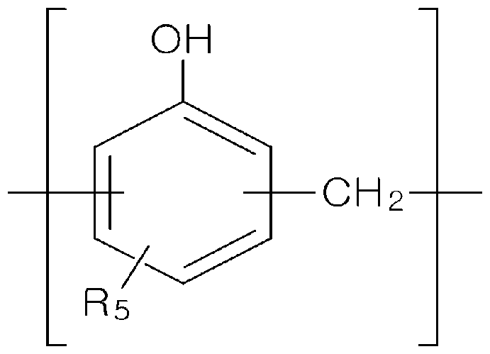
- the photoresist composition further comprises at least one resin D having low absorbance, selected from the group of a novolac-based resin which has low absorbance and at least one of the structural units of Formulae 2 and 3, and
- R is an alkyl or alkoxy group having 1 to 15 carbon atoms, ester, ether, carbonyl, acetal, or alcohol group, and R is hydrogen or an alkyl group having 1 to 5 carbon atoms,
- the photoresist composition comprises the resin D having low absorbance in an amount of 5 to 50 parts by weight based on 100 parts by weight of the base resin.
- the photoresist composition is a non-chemically amplified photoresist.
- the present invention provides a patterning method of a photoresist composition. The method includes applying the photoresist composition; exposing a portion of a photoresist composition layer to light having a main wavelength of 248 nm or less; and removing an exposed portion or a non-exposed portion of the photoresist composition layer.
- the resist composition of the present invention has the desirable physical properties such as sensitivity, resolution, residual film ratio, and coating property and forms a pattern having the desirable profile and depth of focus during a semiconductor process and a flat panel display process using a short wavelength of 248 nm (KrF) or less, even though the resist composition is applied to a non-chemically amplified resist.
- KrF 248 nm
- FIG. 1 is a graph illustrating absorbance of a known novolac-based photoresist composition
- FIGS. 2 and 3 are graphs illustrating light transmissivity at 248 nm and 193 nm in
- FIG. 4A to 4E are SEM pictures illustrating patterns of photoresist compositions of
- FIG. 5 is a graph illustrating sensitivity in Examples according to the present invention. Best Mode for Carrying Out the Invention
- a photoresist composition according to the present invention contains a novolac- based resin, a photosensitizer, and a low molecular substance having low absorbance.
- the low molecular substance having low absorbance has an absorbance that is lower than that of the novolac-based resin at one or more wavelengths of 248 nm, 193 nm, and 157 nm.
- the composition is used at a wavelength of 248 nm or less.
- the resist composition according to the present invention contains the low molecular substance having low absorbance, which has an absorbance that is lower than that of the novolac-based resin at one or more wavelengths of 248 nm, 193 nm, and 157 nm, as an essential component.
- the novolac-based resin A is a base resin of the photoresist in the related art, and a typical novolac based resin may be used in the present invention.
- a phenol compound and aldehyde may be subjected to condensation in the presence of an acid catalyst to produce the novolac- based resin A.
- phenol compound examples include phenol, o-, m-, or p-cresol, 2,3-, 2,5-,
- aldehyde examples include aliphatic aldehydes such as formaldehyde, ace- toaldehyde, propionaldehyde, n-butylaldehyde, isobutylaldehyde, pivalaldehyde, n- hexylaldehyde, and acroleinaldehyde and crotonaldehyde; alicyclic compounds such as cyclohexyaldehyde, cyclopentanealdehyde, furfural and furyl acrolein; aromatic aldehydes such as benzaldehyde, o-, m-, or p-methylbenzaldehyde, p- ethylbenzaldehyde, 2,4-, 2,5-, 3,4-, or 3,5-dimethylbenzaldehyde, o-, m-, or p- hydroxybenzaldehyde, o-,
- Aldehydes may be used alone or as a mixture of two or more species. It is preferable to use formaldehyde that can be easily purchased.
- Examples of acid catalysts that can be used to perform condensation of a phenol compound and aldehyde include inorganic acid such as hydrochloric acid, sulfuric acid, perchloric acid, and phosphoric acid; organic acid such as formic acid, acetic acid, oxalic acid, trichloroacetic acid, and p-toluenesulfonic acid; and divalent metal salts such as zinc acetate, zinc chloride, and manganese acetate.
- inorganic acid such as hydrochloric acid, sulfuric acid, perchloric acid, and phosphoric acid
- organic acid such as formic acid, acetic acid, oxalic acid, trichloroacetic acid, and p-toluenesulfonic acid
- divalent metal salts such as zinc acetate, zinc chloride, and manganese acetate.
- the acid catalysts may be used alone or as a mixture of two or more species.
- the condensation reaction may be performed, for example, at a temperature in the range of 60 to 12O 0 C for 2 to 30 hours, according to a typical process.
- Examples of the photosensitizer B include a photosensitizer that is typically used in the resist field. Particularly, a quinone diazo type radiation-photosensitizer may be used, and examples thereof include diazonaphthoquinone.
- o-quinone diazosulfonic acid ester of a compound having one or more phenolic hydroxyl groups may be used. It is preferable to use 1,2-naphthoquinone diazo-5- or 4-sulfonic acid ester or 1,2-benzoquinone diazo-4- sulfonic acid ester of a polyhydroxy compound having three or more phenolic hydroxyl groups.
- the compounds having the hydroxyl groups and o-quinone diazosulfonic acid halides may be reacted with each other in the presence of a base such as triethylamine to produce the above-mentioned esters.
- o-quinone diazosulfonic acid halides it is preferable to use 1,2-naphthoquinone diazo-5-sulfonic acid chloride.
- the quinone diazo type radiation-photosensitizers may be used alone or as a mixture of one or two agents.
- the amount of photosensitizer B is not limited, but it is preferable that the amount be 30 to 60 parts by weight based on 100 parts by weight of no volac -based resin A.
- the photosensitizer B is contained in the amount of 30 to 60 parts by weight, a developing speed is desirably maintained during exposure, thus forming required patterns.
- the present invention is useful to obtain a non-chemically amplified photoresist that does not contain a photoacid generator by adding the photosensitizer B thereto.
- a photoacid generator by adding the photosensitizer B thereto.
- disadvantages of a chemically amplified photoresist can be avoided.
- the addition of the photoacid generator is not excluded in the present invention.
- Low molecular substance having low absorbance Preferable examples of the low molecular substance C having low absorbance include a compound represented by the following Formula 1.
- R and R are independently hydrogen, hydroxy, or an alkyl group having 1 to 10 carbon atoms, and n is a natural number in the range of 1 to 5.
- n is in the range of 1 to 5, the light transmissivity and sensitivity are increased, thus ensuring desirable patterns. If n is more than 5, the transmissivity is reduced due to absorption of light. Therefore, it is difficult to obtain effects of the low molecular substance C having low absorbance.
- the low molecular substance C having low absorbance is a low molecular compound that has lower absorbance at one or more wavelengths of 248 nm, 193 nm, and 157 nm as compared to the novolac-based resin A. Any low molecular compound may be used in the present invention as long as the compound satisfies the above- mentioned absorbance characteristic.
- the low molecular substance contains oligomers, not polymers.
- the amount of low molecular substance C having low absorbance is not limited, but it is preferable that the amount be 10 to 30 parts by weight based on 100 parts by weight of novolac-based resin A.
- the low molecular substance is contained in the amount of 10 to 30 parts by weight, physical properties of the photoresist are desirable, thus preventing damage to the patterns during development.
- composition of the present invention contains a resin D that has lower absorbance at one or more wavelengths of 248 nm, 193 nm, and 157 nm as compared to the novolac-based resin A, in addition to the low molecular substance C having low absorbance.
- the resin D having low absorbance When the resin D having low absorbance is added to the resist composition, it is preferable to select the resin having low absorbance that can satisfy physical properties required from the resist composition.
- the resin D having low absorbance preferably has a main frame of the polyhydroxystyrene-based resin or novolac-based resin to improve physical properties of the resist.
- the resin D preferably includes a functional group or side branch having desirable transmissivity at a relatively short wavelength.
- the polyhydroxystyrene-based resin that does not have reactivity to the photosensitizer may be used as the polyhydroxystyrene-based resin having low absorbance.
- Examples of the resin D having low absorbance are selected from the group of a novolac-based resin which has low absorbance and at least one of the structural units of Formulae 2 and 3, and a polyhydroxystyrene-based resin which has low absorbance and a structural unit of Formula 4.
- the resist composition may contain at least one of the resins D having low absorbance.
- R is any one of alkyl or alkoxy group having 1 to 15 carbon atoms, ester, ether, carbonyl, acetal, and alcohol group, and R is hydrogen or an alkyl group having 1 to 5 carbon atoms.
- R is an alkyl group having 1 to 5 carbon atoms.
- R is hydrogen or an alkyl group having 1 to 15 carbon atoms.
- R , 3 i any one of alkyl or alkoxy group having 1 to 15 carbon
- the amount of resin D having low absorbance is not limited, but it is preferable that the amount be 5 to 50 parts by weight based on 100 parts by weight of novolac-based resin A.
- the resin D is contained in the amount of 5 to 50 parts by weight, the reactivity between the novolac-based resin and the photosensitizer is desirable, thus preventing damage to patterns during development.
- the weight average molecular weight of resin D having low absorbance is not limited, but it is preferable that the weight average molecular weight be in the range of 3,000 to 20,000 (based on polystyrene), which is obtained by using a gel permeation chromatography (GPC) method.
- GPC gel permeation chromatography
- the weight average molecular weight is in the range of 3,000 to 20,000, the light transmissivity is desirable, accordingly, the resin reacts with a KrF exposure source to form patterns even though A photoresist containing the resin D according to the present invention is a non-chemically amplified resist.
- the low molecular substance C having low absorbance and the resin D having low absorbance may be optionally added to the resist to reduce the concentration of the novolac-based resin A, thus improving the light transmissivity at a wavelength of 248 nm (KrF) or less.
- KrF 248 nm
- micropatterns can be formed at a short wavelength and physical properties of the resist can be desirably satisfied.
- the sensitivity can be improved.
- the photoresist composition according to the present invention may further contain components that are known in the related art.
- the components that are known to be added to the novolac-based photoresist composition may be used in the present invention.
- a solvent may be further contained in order to easily perform coating.
- the photoresist composition according to the present invention is applied on a substrate such as a silicon wafer as a resist solution.
- a substrate such as a silicon wafer as a resist solution.
- the above-mentioned components are dissolved in the solvent to produce the resist solution and the resist solution thusly produced is applied on the substrate.
- Any solvent may be used as long as the solvent can dissolve the components, be dried at a predetermined rate, and be used to form a uniform and smooth coating layer. That is, the typical solvent may be used.
- the solvents include glycol ether esters such as ethyl cellosolve acetate, methyl cellosolve acetate, propylene glycol monomethyl ether acetate, and propylene glycol monoethyl ether acetate; glycol ethers such as ethyl cellosolve, methyl cellosolve, propylene glycol monomethyl ether, and propylene glycol monoethyl ether; esters such as ethyl lactate, butyl acetate, amyl acetate, and ethyl pyruvate; ketones such as 2- heptanone and cyclohexanone; and cyclic esters such as g-butyrolactone.
- the solvents may be used alone or as a mixture of two or more species.
- the photoresist composition according to the present invention contains the resin having low absorbance to increase the light transmissivity at a wavelength of 248 nm by 10 to 35% as compared to the case of when the absorbance is measured by using a UV-Vis spectroscope. Furthermore, even though the resin having low absorbance is added, desirable physical properties of the photoresist composition can be ensured.
- the present invention provides a method of forming a pattern of the photoresist composition.
- the method of forming the pattern of the photoresist composition according to the present invention includes applying the photoresist composition, exposing a portion of the photoresist composition layer to light having a wavelength of 248 nm or less, and removing an exposed portion or a non-exposed portion of the photoresist composition layer.
- the composition is applied on a base substrate (illustrating, but non-limiting examples of the base substrate include glass or a silicon wafer) or the resist composition layer containing solids and subjected to predrying to remove a volatile component such as a solvent, thus forming a flat coating film.
- the thickness of the coating film is not limited, but preferably in the range of 1 to 3 mm.
- the base substrate may be a silicon wafer which is treated with hexamethyldisilazane and includes TiN deposited thereon.
- the process of applying the photoresist is not limited, but may be simply performed by using a spin coater. After the application, drying and then a prebake are performed on a hot plate at 100 0 C for 60 sec.
- a predetermined portion of the coating film is selectively exposed to light emitted from a light source at an exposure wavelength of 248 nm or less by using a mask.
- parallel rays are uniformly radiated on the entire exposed portion and a mask aligner or a stepper is used so as to precisely align the mask with the substrate.
- the type of light source at the exposure wavelength of 248 nm or less is not limited, but may be at least one selected from KrF (248 nm), ArF (193 nm), F (157 nm), and EUV (65 nm).
- the development is performed by using an alkali developing solution.
- the prebake may be performed on the hot plate at 100 0 C for 60 sec before the development, if necessary.
- Various types of alkali solutions known in the related art may be used as the alkali developing solution.
- tetramethylammonium hydroxide and (2-hydroxyethyl)trimethylammonium hydroxide are used in an aqueous solution form.
- a post exposure bake may be performed at a temperature in the range of 150 to 23O 0 C for 10 to 60 min if necessary.
- Examples 1 to 4 and Comparative Examples 1 and 2 Preparation of a photoresist composition
- the compositions were mixed according to the composition ratio described in Table 1 to prepare the photoresist composition.
- Table 1 Table 1
- a-1 m/p cresol novolac-based resin (manufactured by Sumitomo Chemical, Co., Ltd.)
- a-2 polyhydroxystyrene-based resin (manufactured by Sumitomo Chemical, Co., Ltd.)
- b- 1 diazonaphthoquinone type photosensitizer (manufactured by Sumitomo Chemical, Co., Ltd.)
- c-1 1,4-cyclohexanediol (manufactured by Sigma- Aldrich, Corp.)
- d-1 resin having low absorbance, which is represented by Formula 4 and in which
- R is hydrogen
- e- 1 diazo type photoacid generator (manufactured by Wako, Corp.)
- the light transmissivity of the novolac-based photoresist composition of Comparative Example 1 was 14.82% at a wavelength of 193 nm.
- the light transmissivities were 18.1%, 19.35%, 20.9%, and 21.25%. Therefore, it can be seen that the light transmissivity was increased by 149.32%, 206.2%, 276.85%, and 292.78% in Examples 1 to 4 as compared to Comparative Example 1.
- the resulting film was exposed on the hot plate and subjected to post-exposure bake(PEB) at 9O 0 C for 60 sec. Paddle development was performed for 60 sec by using 2.38% tetramethylammonium hydroxide (TMAH) aqueous solution. Subsequently, rinsing was performed by using pure water to form a 0.4 mm line and space (1:1) pattern.
- PEB post-exposure bake
- TMAH tetramethylammonium hydroxide
- Example 1 and Examples according to the above-mentioned procedure. Exposure energy was changed to obtain minimum exposure energy when the pattern was formed on the bottom of the photoresist film, and the sensitivity was then measured. The results are shown in FIG. 5.
- the x-axis denotes the sensitivity (unit: mJ/cm ), and the y-axis denotes Comparative Example 1 and Examples 1 to 4.
- Comparative Example 1 was 200 mJ/cm . However, in the case of the photoresists of
- the patterns were formed on the silicon wafer on which the silicon oxide film was deposited by using the photoresist compositions of Example 4 and Comparative Example 2 according to the above-mentioned procedure.
- the resulting wafer was dipped in BOE etchant (0.5 parts by weight of 50% hydrofluoric acid based on 100 parts by weight of 40% ammonium fluoride) at 23 0 C for 440 sec.
- BOE etchant 0.5 parts by weight of 50% hydrofluoric acid based on 100 parts by weight of 40% ammonium fluoride
Landscapes
- Physics & Mathematics (AREA)
- Spectroscopy & Molecular Physics (AREA)
- General Physics & Mathematics (AREA)
- Chemical & Material Sciences (AREA)
- Engineering & Computer Science (AREA)
- Ceramic Engineering (AREA)
- Materials For Photolithography (AREA)
- Exposure And Positioning Against Photoresist Photosensitive Materials (AREA)
Abstract
Description


Claims



Priority Applications (3)
| Application Number | Priority Date | Filing Date | Title |
|---|---|---|---|
| US12/376,107 US8211614B2 (en) | 2006-08-04 | 2007-08-02 | Photoresist composition and patterning method thereof |
| CN2007800291537A CN101501570B (en) | 2006-08-04 | 2007-08-02 | Photoresist composition and patterning method thereof |
| JP2009522719A JP5057530B2 (en) | 2006-08-04 | 2007-08-02 | Positive photoresist composition and pattern forming method thereof |
Applications Claiming Priority (2)
| Application Number | Priority Date | Filing Date | Title |
|---|---|---|---|
| KR10-2006-0073900 | 2006-08-04 | ||
| KR20060073900 | 2006-08-04 |
Publications (1)
| Publication Number | Publication Date |
|---|---|
| WO2008016270A1 true WO2008016270A1 (en) | 2008-02-07 |
Family
ID=38997406
Family Applications (1)
| Application Number | Title | Priority Date | Filing Date |
|---|---|---|---|
| PCT/KR2007/003726 Ceased WO2008016270A1 (en) | 2006-08-04 | 2007-08-02 | Photoresist composition and patterning method thereof |
Country Status (6)
| Country | Link |
|---|---|
| US (1) | US8211614B2 (en) |
| JP (1) | JP5057530B2 (en) |
| KR (1) | KR101363738B1 (en) |
| CN (1) | CN101501570B (en) |
| TW (1) | TWI416252B (en) |
| WO (1) | WO2008016270A1 (en) |
Families Citing this family (6)
| Publication number | Priority date | Publication date | Assignee | Title |
|---|---|---|---|---|
| JP5708522B2 (en) * | 2011-02-15 | 2015-04-30 | 信越化学工業株式会社 | Resist material and pattern forming method using the same |
| JP5674506B2 (en) * | 2011-02-25 | 2015-02-25 | 東京応化工業株式会社 | Positive resist composition and resist pattern forming method |
| WO2012137838A1 (en) * | 2011-04-08 | 2012-10-11 | 太陽インキ製造株式会社 | Photosensitive composition, hardened coating films therefrom, and printed wiring boards using same |
| JP6284849B2 (en) * | 2013-08-23 | 2018-02-28 | 富士フイルム株式会社 | Laminate |
| WO2016084495A1 (en) * | 2014-11-25 | 2016-06-02 | Dic株式会社 | Novolac type phenol resin, manufacturing method therefor, photosensitive composition, resist material and coating film |
| KR102417180B1 (en) | 2017-09-29 | 2022-07-05 | 삼성전자주식회사 | Photoresist composition for DUV, patterning method, and method of manufacturing semiconductor device |
Citations (5)
| Publication number | Priority date | Publication date | Assignee | Title |
|---|---|---|---|---|
| WO2000034829A1 (en) * | 1998-12-10 | 2000-06-15 | Clariant International Ltd. | Positively photosensitive resin composition |
| JP2004258099A (en) * | 2003-02-24 | 2004-09-16 | Tokyo Ohka Kogyo Co Ltd | Positive photoresist composition and method for forming resist pattern |
| WO2004088424A2 (en) * | 2003-04-01 | 2004-10-14 | Az Electronic Materials Usa Corp. | Photoresist compositions |
| WO2005007719A2 (en) * | 2003-07-16 | 2005-01-27 | Tokyo Ohka Kogyo Co., Ltd. | Positive photoresist composition and method of forming resist pattern |
| JP2005114920A (en) * | 2003-10-06 | 2005-04-28 | Tokyo Ohka Kogyo Co Ltd | Positive photoresist composition for injection nozzle coating method and method for forming resist pattern |
Family Cites Families (21)
| Publication number | Priority date | Publication date | Assignee | Title |
|---|---|---|---|---|
| US4123279A (en) * | 1974-03-25 | 1978-10-31 | Fuji Photo Film Co., Ltd. | Light-sensitive o-quinonediazide containing planographic printing plate |
| JPS616647A (en) * | 1984-06-20 | 1986-01-13 | Konishiroku Photo Ind Co Ltd | Photosensitive composition for postive type photosensitive lighographic printing plafe |
| JPS62251739A (en) * | 1986-04-24 | 1987-11-02 | Fuji Photo Film Co Ltd | Photosensitive composition |
| JPS63163340A (en) * | 1986-12-25 | 1988-07-06 | Matsushita Electric Ind Co Ltd | pattern forming material |
| US5178986A (en) * | 1988-10-17 | 1993-01-12 | Shipley Company Inc. | Positive photoresist composition with naphthoquinonediazidesulfonate of oligomeric phenol |
| JPH05113666A (en) * | 1991-10-21 | 1993-05-07 | Nippon Zeon Co Ltd | Resist composition |
| JPH08179502A (en) | 1994-12-27 | 1996-07-12 | Mitsui Toatsu Chem Inc | Photosensitive resin composition |
| US5932396A (en) * | 1996-10-18 | 1999-08-03 | Tdk Corporation | Method for forming magnetic poles in thin film magnetic heads |
| JPH10254137A (en) * | 1997-03-11 | 1998-09-25 | Nec Corp | Chemical amplification type resist |
| JP3055617B2 (en) * | 1997-08-27 | 2000-06-26 | 日本電気株式会社 | Negative photoresist composition and pattern forming method using the same |
| EP1314552B1 (en) * | 1998-04-06 | 2009-08-05 | FUJIFILM Corporation | Photosensitive resin composition |
| KR20000076585A (en) * | 1999-02-02 | 2000-12-26 | 미우라 아끼라 | Radiation-sensitive resin composition |
| JP4480835B2 (en) | 1999-02-12 | 2010-06-16 | ローム・アンド・ハース・エレクトロニック・マテリアルズ,エル.エル.シー. | Positive radiation sensitive resin composition |
| JP3998901B2 (en) | 1999-08-31 | 2007-10-31 | 東京応化工業株式会社 | Photosensitive substrate, resist pattern forming method using the same, and positive resist composition |
| JP2002296774A (en) * | 2001-03-30 | 2002-10-09 | Fuji Photo Film Co Ltd | Original plate for planographic printing plate |
| JP4152852B2 (en) * | 2003-09-30 | 2008-09-17 | 東京応化工業株式会社 | POSITIVE PHOTORESIST COMPOSITION FOR DISCHARGE NOZZLE TYPE COATING METHOD AND METHOD FOR FORMING RESIST PATTERN |
| US7867687B2 (en) * | 2003-10-15 | 2011-01-11 | Intel Corporation | Methods and compositions for reducing line wide roughness |
| JP4513965B2 (en) * | 2004-03-31 | 2010-07-28 | 日本ゼオン株式会社 | Radiation sensitive resin composition |
| KR20070029731A (en) * | 2004-06-01 | 2007-03-14 | 이 아이 듀폰 디 네모아 앤드 캄파니 | UV-transparent alkanes and their use in vacuum and far ultraviolet applications |
| US7803510B2 (en) * | 2005-08-17 | 2010-09-28 | Fujifilm Electronic Materials U.S.A., Inc. | Positive photosensitive polybenzoxazole precursor compositions |
| JP2007148258A (en) * | 2005-11-30 | 2007-06-14 | Daicel Chem Ind Ltd | Resist composition |
-
2007
- 2007-08-02 WO PCT/KR2007/003726 patent/WO2008016270A1/en not_active Ceased
- 2007-08-02 CN CN2007800291537A patent/CN101501570B/en active Active
- 2007-08-02 JP JP2009522719A patent/JP5057530B2/en active Active
- 2007-08-02 US US12/376,107 patent/US8211614B2/en active Active
- 2007-08-02 KR KR1020070077716A patent/KR101363738B1/en active Active
- 2007-08-03 TW TW096128656A patent/TWI416252B/en active
Patent Citations (5)
| Publication number | Priority date | Publication date | Assignee | Title |
|---|---|---|---|---|
| WO2000034829A1 (en) * | 1998-12-10 | 2000-06-15 | Clariant International Ltd. | Positively photosensitive resin composition |
| JP2004258099A (en) * | 2003-02-24 | 2004-09-16 | Tokyo Ohka Kogyo Co Ltd | Positive photoresist composition and method for forming resist pattern |
| WO2004088424A2 (en) * | 2003-04-01 | 2004-10-14 | Az Electronic Materials Usa Corp. | Photoresist compositions |
| WO2005007719A2 (en) * | 2003-07-16 | 2005-01-27 | Tokyo Ohka Kogyo Co., Ltd. | Positive photoresist composition and method of forming resist pattern |
| JP2005114920A (en) * | 2003-10-06 | 2005-04-28 | Tokyo Ohka Kogyo Co Ltd | Positive photoresist composition for injection nozzle coating method and method for forming resist pattern |
Also Published As
| Publication number | Publication date |
|---|---|
| TW200811596A (en) | 2008-03-01 |
| JP2009545768A (en) | 2009-12-24 |
| JP5057530B2 (en) | 2012-10-24 |
| CN101501570A (en) | 2009-08-05 |
| CN101501570B (en) | 2012-07-25 |
| TWI416252B (en) | 2013-11-21 |
| KR20080012781A (en) | 2008-02-12 |
| US20100203444A1 (en) | 2010-08-12 |
| KR101363738B1 (en) | 2014-02-18 |
| US8211614B2 (en) | 2012-07-03 |
Similar Documents
| Publication | Publication Date | Title |
|---|---|---|
| EP2203783B1 (en) | Thick film resists | |
| JP4359151B2 (en) | Photoresist composition containing acetal and ketal as solvent | |
| US8101333B2 (en) | Method for formation of miniaturized pattern and resist substrate treatment solution for use in the method | |
| WO2013064892A2 (en) | Nanocomposite positive photosensitive composition and use thereof | |
| JP3238465B2 (en) | Pattern forming resist and pattern forming method | |
| US8211614B2 (en) | Photoresist composition and patterning method thereof | |
| US20100028817A1 (en) | Solution for treatment of resist substrate after development processing and method for treatment of resist substrate using the same | |
| EP0919012B1 (en) | Positive photoresist composition containing a 2,4-dinitro-1-naphthol | |
| JP4340932B2 (en) | Negative radiation sensitive resin composition | |
| JP3722538B2 (en) | Positive photoresist composition | |
| KR101316192B1 (en) | Photoresist composition | |
| JP3259263B2 (en) | Negative radiation-sensitive resin composition | |
| JP4759895B2 (en) | Resin for photoresist and photoresist composition | |
| JP4302423B2 (en) | Resin for base material, base material, and multilayer resist pattern forming method | |
| JP2005010487A (en) | Method for forming resist pattern | |
| KR20080012684A (en) | Photoresist composition and pattern formation method thereof | |
| KR20090049423A (en) | Photoresist composition and pattern formation method using the same | |
| JPH10274854A (en) | Method of forming hole pattern using photoresist | |
| JP4067260B2 (en) | Positive photoresist composition | |
| JP3636503B2 (en) | Radiation sensitive resin composition | |
| JP2005010486A (en) | Method for forming resist pattern | |
| JP4759894B2 (en) | Photoresist composition | |
| JPH09166876A (en) | Intermediate film composition and method for forming photosensitive film on substrate using the same | |
| JPH0668625B2 (en) | Developer and method for positive photoresist | |
| KR20110035528A (en) | Positive photoresist composition |
Legal Events
| Date | Code | Title | Description |
|---|---|---|---|
| WWE | Wipo information: entry into national phase |
Ref document number: 200780029153.7 Country of ref document: CN |
|
| 121 | Ep: the epo has been informed by wipo that ep was designated in this application |
Ref document number: 07807935 Country of ref document: EP Kind code of ref document: A1 |
|
| WWE | Wipo information: entry into national phase |
Ref document number: 2009522719 Country of ref document: JP Ref document number: 12376107 Country of ref document: US |
|
| NENP | Non-entry into the national phase |
Ref country code: DE |
|
| NENP | Non-entry into the national phase |
Ref country code: RU |
|
| 122 | Ep: pct application non-entry in european phase |
Ref document number: 07807935 Country of ref document: EP Kind code of ref document: A1 |