WO2007119954A1 - Preparing method for organic thin layer of organic light emitting devices using electrochemical deposition - Google Patents

Preparing method for organic thin layer of organic light emitting devices using electrochemical deposition Download PDF

Info

Publication number
WO2007119954A1
WO2007119954A1 PCT/KR2007/001721 KR2007001721W WO2007119954A1 WO 2007119954 A1 WO2007119954 A1 WO 2007119954A1 KR 2007001721 W KR2007001721 W KR 2007001721W WO 2007119954 A1 WO2007119954 A1 WO 2007119954A1
Authority
WO
WIPO (PCT)
Prior art keywords
organic thin
light emitting
thin layer
emitting device
organic
Prior art date
Legal status (The legal status is an assumption and is not a legal conclusion. Google has not performed a legal analysis and makes no representation as to the accuracy of the status listed.)
Ceased
Application number
PCT/KR2007/001721
Other languages
French (fr)
Inventor
Chan-Seok Park
Chong-Chan Lee
Sang-Ook Kang
Won-Sik Han
Ho-Jin Son
Jong-Hyub Baek
Current Assignee (The listed assignees may be inaccurate. Google has not performed a legal analysis and makes no representation or warranty as to the accuracy of the list.)
Dongjin Semichem Co Ltd
Original Assignee
Dongjin Semichem Co Ltd
Priority date (The priority date is an assumption and is not a legal conclusion. Google has not performed a legal analysis and makes no representation as to the accuracy of the date listed.)
Filing date
Publication date
Application filed by Dongjin Semichem Co Ltd filed Critical Dongjin Semichem Co Ltd
Priority to JP2009505292A priority Critical patent/JP5113153B2/en
Priority to DE112007000924T priority patent/DE112007000924T5/en
Publication of WO2007119954A1 publication Critical patent/WO2007119954A1/en
Anticipated expiration legal-status Critical
Ceased legal-status Critical Current

Links

Classifications

    • CCHEMISTRY; METALLURGY
    • C09DYES; PAINTS; POLISHES; NATURAL RESINS; ADHESIVES; COMPOSITIONS NOT OTHERWISE PROVIDED FOR; APPLICATIONS OF MATERIALS NOT OTHERWISE PROVIDED FOR
    • C09KMATERIALS FOR MISCELLANEOUS APPLICATIONS, NOT PROVIDED FOR ELSEWHERE
    • C09K11/00Luminescent materials, e.g. electroluminescent or chemiluminescent
    • C09K11/06Luminescent materials, e.g. electroluminescent or chemiluminescent containing organic luminescent materials
    • HELECTRICITY
    • H05ELECTRIC TECHNIQUES NOT OTHERWISE PROVIDED FOR
    • H05BELECTRIC HEATING; ELECTRIC LIGHT SOURCES NOT OTHERWISE PROVIDED FOR; CIRCUIT ARRANGEMENTS FOR ELECTRIC LIGHT SOURCES, IN GENERAL
    • H05B33/00Electroluminescent light sources
    • H05B33/12Light sources with substantially two-dimensional [2D] radiating surfaces
    • H05B33/14Light sources with substantially two-dimensional [2D] radiating surfaces characterised by the chemical or physical composition or the arrangement of the electroluminescent material, or by the simultaneous addition of the electroluminescent material in or onto the light source
    • HELECTRICITY
    • H10SEMICONDUCTOR DEVICES; ELECTRIC SOLID-STATE DEVICES NOT OTHERWISE PROVIDED FOR
    • H10KORGANIC ELECTRIC SOLID-STATE DEVICES
    • H10K85/00Organic materials used in the body or electrodes of devices covered by this subclass
    • H10K85/40Organosilicon compounds, e.g. TIPS pentacene
    • HELECTRICITY
    • H10SEMICONDUCTOR DEVICES; ELECTRIC SOLID-STATE DEVICES NOT OTHERWISE PROVIDED FOR
    • H10KORGANIC ELECTRIC SOLID-STATE DEVICES
    • H10K85/00Organic materials used in the body or electrodes of devices covered by this subclass
    • H10K85/60Organic compounds having low molecular weight
    • H10K85/649Aromatic compounds comprising a hetero atom
    • H10K85/657Polycyclic condensed heteroaromatic hydrocarbons
    • H10K85/6572Polycyclic condensed heteroaromatic hydrocarbons comprising only nitrogen in the heteroaromatic polycondensed ring system, e.g. phenanthroline or carbazole
    • CCHEMISTRY; METALLURGY
    • C09DYES; PAINTS; POLISHES; NATURAL RESINS; ADHESIVES; COMPOSITIONS NOT OTHERWISE PROVIDED FOR; APPLICATIONS OF MATERIALS NOT OTHERWISE PROVIDED FOR
    • C09KMATERIALS FOR MISCELLANEOUS APPLICATIONS, NOT PROVIDED FOR ELSEWHERE
    • C09K2211/00Chemical nature of organic luminescent or tenebrescent compounds
    • C09K2211/10Non-macromolecular compounds
    • C09K2211/1003Carbocyclic compounds
    • C09K2211/1007Non-condensed systems
    • CCHEMISTRY; METALLURGY
    • C09DYES; PAINTS; POLISHES; NATURAL RESINS; ADHESIVES; COMPOSITIONS NOT OTHERWISE PROVIDED FOR; APPLICATIONS OF MATERIALS NOT OTHERWISE PROVIDED FOR
    • C09KMATERIALS FOR MISCELLANEOUS APPLICATIONS, NOT PROVIDED FOR ELSEWHERE
    • C09K2211/00Chemical nature of organic luminescent or tenebrescent compounds
    • C09K2211/10Non-macromolecular compounds
    • C09K2211/1003Carbocyclic compounds
    • C09K2211/1011Condensed systems
    • CCHEMISTRY; METALLURGY
    • C09DYES; PAINTS; POLISHES; NATURAL RESINS; ADHESIVES; COMPOSITIONS NOT OTHERWISE PROVIDED FOR; APPLICATIONS OF MATERIALS NOT OTHERWISE PROVIDED FOR
    • C09KMATERIALS FOR MISCELLANEOUS APPLICATIONS, NOT PROVIDED FOR ELSEWHERE
    • C09K2211/00Chemical nature of organic luminescent or tenebrescent compounds
    • C09K2211/10Non-macromolecular compounds
    • C09K2211/1018Heterocyclic compounds
    • C09K2211/1025Heterocyclic compounds characterised by ligands
    • C09K2211/1029Heterocyclic compounds characterised by ligands containing one nitrogen atom as the heteroatom
    • CCHEMISTRY; METALLURGY
    • C09DYES; PAINTS; POLISHES; NATURAL RESINS; ADHESIVES; COMPOSITIONS NOT OTHERWISE PROVIDED FOR; APPLICATIONS OF MATERIALS NOT OTHERWISE PROVIDED FOR
    • C09KMATERIALS FOR MISCELLANEOUS APPLICATIONS, NOT PROVIDED FOR ELSEWHERE
    • C09K2211/00Chemical nature of organic luminescent or tenebrescent compounds
    • C09K2211/10Non-macromolecular compounds
    • C09K2211/1018Heterocyclic compounds
    • C09K2211/1025Heterocyclic compounds characterised by ligands
    • C09K2211/1096Heterocyclic compounds characterised by ligands containing other heteroatoms
    • HELECTRICITY
    • H10SEMICONDUCTOR DEVICES; ELECTRIC SOLID-STATE DEVICES NOT OTHERWISE PROVIDED FOR
    • H10KORGANIC ELECTRIC SOLID-STATE DEVICES
    • H10K71/00Manufacture or treatment specially adapted for the organic devices covered by this subclass
    • H10K71/10Deposition of organic active material
    • H10K71/16Deposition of organic active material using physical vapour deposition [PVD], e.g. vacuum deposition or sputtering
    • HELECTRICITY
    • H10SEMICONDUCTOR DEVICES; ELECTRIC SOLID-STATE DEVICES NOT OTHERWISE PROVIDED FOR
    • H10KORGANIC ELECTRIC SOLID-STATE DEVICES
    • H10K71/00Manufacture or treatment specially adapted for the organic devices covered by this subclass
    • H10K71/40Thermal treatment, e.g. annealing in the presence of a solvent vapour

Definitions

  • the invention relates to a method for preparing an organic thin layer of organic light emitting device using electrochemical deposition and more particularly, to a method for preparing an organic thin layer of organic light emitting device that has simple process by virtue of the use of monomolecular compounds that are easily purchased and prepared, has high productivity, makes it easy to control the thickness of thin layers to be prepared and has excellent adhesion to substrates and further, fundamentally improves erosion that may occur in a firstly-formed organic thin layer during the process of formation of a second organic thin layer especially when two or more organic thin layers are to be prepared in OLED devices and has excellent morphology stability, and an organic light emitting device prepared by the same method.
  • Background Art
  • OLED organic light emitting devices
  • General organic EL devices have a structure of an anode which is formed on the top of a substrate, a light emitting layer in the form of an organic thin film which is formed on the anode, and a cathode formed thereon in sequence. Further, they may have a hole injection layer or hole transport layer between the anode and the light emitting layer, or they may have a electron transport layer or electron injection layer between the light emitting layer and the cathode.
  • the hole injection layer, hole transport layer, electron transport layer and electron injection layer are organic thin layers consisting of organic compounds.
  • Such organic thin layers are formed through vacuum heat deposition, sputtering or spin coating.
  • the vacuum heat deposition or sputtering requires expensive equipments and has low productivity
  • the spin coating involves the problem that when two or more organic thin layers are formed, the previously-formed lower layer is melted by solvents in the process of spin coating of upper layer.
  • the present invention provides a method for preparing an organic thin layer of organic light emitting device comprising one or more organic thin layers between an anode and cathode, characterized in that the organic thin layer is formed by electrochemical deposition of a compound having bis(phenylcarbazol) group in molecule.
  • the compound having bis(phenylcarbazol) group in molecule is represented by formula 1 :
  • the invention provides the organic thin layer of organic light emitting device prepared by the above method. [13] Also, the invention provides an organic light emitting device comprising the organic thin layer prepared by the above method. [14] Also, the invention comprises a display device comprising the above organic light emitting device.
  • the method for preparation of the organic thin layer of organic light emitting device through electrochemical deposition according to the invention has simple process by virtue of the use of monomolecular compounds that are purchased or easily prepared without requiring special equipments, has high productivity, can make it easy to control the thickness of thin layers to be prepared and can fundamentally improve erosion of the pre-formed organic thin layers that occurred in the preparation of two or more organic thin layers by spin coating.
  • the organic thin layers in accordance with the invention have excellent adhesion to substrates, have uniform surface because their thickness can be adjusted at molecular level, and have excellent morphology stability and especially, in case of the organic thin layers formed through consecutive electrochemical deposition of two or more layers, interfaces between layers are even, erosion due to solvents does not occur, adhesion between interfaces is strong and they have fine patterns. Moreover, as they are not melted in most organic solvents, erosion due to solvents can be fundamentally reduced even in case of forming organic thin layers by known spin coating on the organic thin layers in accordance with the invention. Brief Description of the Drawings
  • Fig. 1 is a cyclic voltammonogram showing electrochemical deposition by a compound having bis(phenylcarbazol) group in a molecule according to an embodiment of the present invention.
  • Fig. 2 is a cyclic voltammonogram showing electrochemical deposition by a compound having bis(phenylcarbazol) group in a molecule according to another embodiment of the invention.
  • Fig. 3 is a cyclic voltammonogram showing electrochemical deposition by a compound having bis(phenylcarbazol) group in a molecule according to still another embodiment of the invention.
  • Fig. 4 is a cyclic voltammonogram showing electrochemical deposition by a compound having one phenylcarbazol group in a molecule according to comparative example of the invention.
  • Fig. 5 is a cyclic voltammonogram showing electrochemical deposition by a compound having bis (phenylcarbazol) group in a molecule according to another embodiment of the invention.
  • Fig. 6 is a cyclic voltammonogram showing electrochemical deposition by a compound having bis (phenylcarbazol) group in a molecule according to still another embodiment of the invention.
  • organic thin layers could be formed using electrochemical deposition by compounds having bis(phenylcarbazol) group in molecules as monomolecular compounds having small molecular weight and have thus completed the invention.
  • the present invention is directed to a method for preparing an organic thin layer of organic light emitting device comprising one or more organic thin films between anode and cathode characterized in that the organic thin layer is formed by electrochemical deposition of a compound having bis(phenylcarbazol) group in molecule.
  • the compound is a compound represented by the above formula 1 or one with two phenyl carbazol groups linked directly.
  • the divalent linking group, -X- is not limited to specific ones as long as phenyl carbazol groups can be bound to its both ends, and -SiR R -, -PR -, -NR
  • R to R are each independently a substituted or unsubstituted alkyl group of C -C , substituted or unsubstituted aryl group of C -C , substituted or unsubstituted hetero ring group of C -C , or substituted or unsubstituted heterocyclic ring group of C -C .
  • alkyl group of C -C include methyl, ethyl, propyl, isobutyl, sec-butyl, pentyl, iso-amyl, hexyl and so on, and one or more hydrogen atoms of the alkyl group may be substituted by a halogen atom, hydroxyl group, nitro group, cyano group, amino group, amidino group, hydrazine, hydrozone, carboxyl group or salt thereof, sulfonic acid group or salt thereof, phosphoric acid or salt thereof, indole, azaindole, alkyl group of C -C , alkenyl group of C -C , alkynyl group of C -C , aryl group of C -C , arylalkyl group of C -C , heteroaryl group of C -C , or het- eroarylalkyl group of C -C and of them
  • the unsubstituted aryl group in above refers to a carbocycle aromatic system of C -
  • the aryl includes aromatic radicals such as phenyl, naphthyl and tetrahydronaphthyl and one or more hydrogen atoms of the aryl group may be substituted by the same substituents as enumerated for the alkyl group.
  • the unsubstituted hetero ring group refers to a monovalent monocyclic or bicyclic aromatic organic compound of 6 to 50 ring atoms containing 1, 2 or 3 hetero atoms selected from N, O, P or S and having C as remaining ring atoms.
  • One or more hydrogen atoms of the hetero aryl group may be substituted by the same substituents as enumerated for the alkyl group.
  • the unsubstituted heterocyclic ring group refers to a ring type moiety formed by the fusion of two or more rings constituting the aryl group or hetero ring as defined above and one or more hydrogen atoms of the heterocyclic ring group may be substituted by the same substituents as enumerated for the alkyl group.
  • n is an integer of 1 to 3
  • R is each independently a hydrogen atom or methyl
  • electrochemical deposition refers to a method of forming organic thin layers by putting substrates to be deposited into a reaction vessel where the above compounds forming the organic thin layers which are intended to deposit and electrolytes are dissolved and depositing the compounds intended to deposit onto the substrates to be deposited by application of power.
  • the compounds forming the organic thin layers which are intended to deposit can be chosen among the above described compounds, depending on the organic thin layers to be formed on the substrates to be deposited, and the organic thin layer is one of the organic layers formed between anode and cathode and can be a hole injection layer (HIL), hole transport layer (HTL), emitting layer (EML), hole blocking layer (HBL), electron transport layer (ETL) or electron injection layer (EIL).
  • HIL hole injection layer
  • HTL hole transport layer
  • EML hole blocking layer
  • ETL electron transport layer
  • EIL electron injection layer
  • Any solvents capable of dissolving the electrolytes and the compounds intended to deposit can be used in the above reaction vessel and as specific examples, there are dichloromethane (CH Cl ), tetrahydrofuran (THF), acetonitrile (CH CN), benzonitrile (C H CN), propylene carbonate (1,2-propanediol cycliccarbonate), and toluene (C H
  • the amount of the solvents to be used is preferably 0.01 to 10 mM on the basis of the concentration of the compounds. If the concentration is too thin, there is a possibility that the electrochemical deposition is not performed properly and if it is too thick, problems may happen in connection with the control of the electrochemical deposition film thickness and voltage drop.
  • the electrolytes that can be used in the reaction vessel are dissolved in the above solvents and they are not limited to specific ones as long as they are able to ionize the compounds intended to deposit when power is applied, and as specific examples, there are Me NBF , Et NBF , Pr NBF , Bu NBF , Me NClO , Et NClO , Pr NClO , Bu NClO 4 , Me 4 NPF 6 , Et 4 NPF 6 , Pr 4 NPF 6 , Bu 4 NPF 6 , LiClO 4 , LiBF 4 , LiPF 6 , and LiBOB.
  • the concentration of the supporting electrolytes is preferably 50 mM to 500 mM. If the concentration of the electrolytes is too thin, such problems as voltage drop may happen.
  • any conventional substrates used to form organic thin layers in OLED devices can be used.
  • they can be a substrate with anode formed thereon; or a substrate on which anode and at least one layer from hole injection layer (HIL), hole transport layer (HTL), emitting layer (EML), hole blocking layer (HBL) and electron transport layer (ETL) are deposited in sequence.
  • HIL hole injection layer
  • HTL hole transport layer
  • EML emitting layer
  • HBL hole blocking layer
  • ETL electron transport layer
  • any substrates used in common organic EL devices can be employed as the substrates and it is preferable to use organic substrates or clear plastic substrates with excellent clearness, surface flatness, easy handling and waterproof.
  • ITO indium tin oxide
  • IZO indium zinc oxide
  • SnO tin oxide
  • ZnO zinc oxide
  • the one or more organic layers among the hole injection layer (HIL), hole transport layer (HTL), emitting layer (EML), hole blocking layer (HBL) and electron transport layer (ETL) to be formed on the substrates to be deposited can be formed by known methods or by the electrochemical deposition of the invention.
  • the above organic layers are formed using the electrochemical deposition of the invention.
  • the electrochemical deposition is preferably used to form the organic thin layers in this step.
  • the cathode can be formed by any known methods and for example, the cathode can be formed by vacuum heat deposition of or sputtering metals for the formation of cathode.
  • metals for the formation of cathode there can be used lithium (Li), magnesium (Mg), aluminum (Al), aluminum-lithium (Al-Li), calcium (Ca), magnesium-indium (Mg-In), magnesium- silver (Mg-Ag) and the like.
  • clear substances such as ITO or IZO can be used as cathode.
  • HIL hole injection layer
  • HTL hole transport layer
  • EML emitting layer
  • HBL hole blocking layer
  • ETL electron transport layer
  • EIL electron injection layer
  • the thickness of the organic thin layers formed through the electrochemical deposition in accordance with the present invention can be adjusted by power cycle control, depending on the required level and it is preferably 10 to 1,000 D and more preferably, 20 to 150 D.
  • power is applied preferably using CV (cyclic voltammetry). Voltage is applied in the range of voltage within potential window showing no oxidation-reduction of solvents or electrolytes or electrodes, and when CV is used, although there are slight variations in each compound, voltage is scanned starting from 0.30 V vs S.C.E. up to 1.65(+0.1) V vs S.C.E. at a voltage scan rate of 0.1 V/s and returned to 0.30 V vs S.C.E.
  • CV cyclic voltammetry
  • electrochemical deposition proceeds.
  • the thickness of thin layers of compounds can be adjusted by varying the number of cycles, the concentration of the compounds, voltage scan rate, voltage scan range and so on.
  • washing step or dry step can be further carried out, if required.
  • electrolyte substances that might be present on the organic thin layers, and those used as the solvent component of the reaction vessel are preferably used as the washing solution.
  • the dry step is not limited to specific ones, and any known dry methods that can be carried out after the formation of known organic thin layers of organic light emitting devices can be applied.
  • the concentration of the compound of the above formula can be 0.5 mM and the concentration of the electrolyte can be 0.1 M.
  • the substrate to be deposited can be a glass substrate with ITO as anode deposited thereon, a substrate of the glass substrate-ITO-hole injection layer being laminated in order, or a substrate of the glass substrate-ITO-hole injection layer- hole transport layer being laminated in order.
  • the compound dissolved in the reaction vessel is deposited onto the substrate to be deposited and the thickness to be deposited can be adjusted by the number of cycles of CV (cyclic voltammetry).
  • the substrate deposited with the above compound may be further deposited with one or more organic thin layers such as electron transport layer and electron injection layer, if necessary, after washing and dry and then, cathode is formed on the organic layers through vacuum heat deposition or sputtering, thereby completing an organic light emitting device.
  • the method for preparation of the organic thin layer of organic light emitting device through electrochemical deposition according to the invention has simple process by virtue of the use of monomolecular compounds that are purchased or easily prepared without requiring special equipments, has high productivity, can make it easy to control the thickness of thin layers to be prepared and can fundamentally improve erosion of the pre-formed organic thin layers that occurred in the preparation of two or more organic thin layers by spin coating.
  • the invention provides the organic thin layers of organic light emitting device prepared by the electrochemical deposition and organic light emitting devices comprising the organic thin layers as well.
  • the organic thin layers have excellent adhesion to substrates, have uniform surface because their thickness can be adjusted at molecular level, and have excellent morphology stability and especially, in case of the organic thin layers formed through consecutive electrochemical deposition of two or more layers, interfaces between layers are even, erosion due to solvents does not occur, adhesion between interfaces is strong and they have fine patterns.
  • the organic thin layers in accordance with the invention are not melted in most organic solvents, erosion due to solvents can be fundamentally reduced even in case of forming organic thin layers by known spin coating.
  • BAS 100 electrochemical analyzer was used for the CV experiment.
  • Three-electrode system - glassy carbon as a working electrode, platinum electric wire as a counter electrode and silver electric wire as a reference electrode - was used.
  • Methylene chloride that is neat, distilled and degassed was used as a solvent and 0.1 M tetra-normal-butylammonium hexafluorophosphate was used as an electrolyte.
  • Normal-butyllithium diluted in 1,4-dibromobenzene 2.5 M hexane was purchased from Aldrich Co., Ltd. and used without further purification.
  • Teflon magnetic stir bar 1,4-dibromobenzene (25.184 g, 200 mmol), carbazol (8.36 g, 50 mmol), K CO (13.82 g, 100 mmol), and CuSO (7.98 g, 50 mmol) were put in a 100-mL one-neck flask and stirred at 210 0 C for 16 hours without solvents. After the completion of the reaction, the mixture was diluted with methylenechloride and filtered and then, the filtered solution was washed with distilled water and brine. The thus obtained organic layer was dehydrated using MgSO .
  • Bromophenylcarbazol was converted into an organic lithium compound in tetrahydrofuran (THF) solvent using normal-butyllithium at -78 0 C and then reacted with trichlorosilane, dimethyldichloridesilane, and trichloromethylsilane to synthesize mono-, bis-, tirs-(9-(phenylcarbozol)) (Compound 4-6), respectively with yields of 40-75%.
  • Compound 5 and Compound 6 were separated through silica gel column and Compound 4 could be obtained by re- crystallization using ether without separation with column.
  • the method for preparation of the organic thin layer of organic light emitting device through electrochemical deposition according to the invention has simple process by virtue of the use of monomolecular compounds that are purchased or easily prepared without requiring special equipments, has high productivity, can make it easy to control the thickness of thin layers to be prepared and can fundamentally improve erosion of the pre-formed organic thin layers that occurred in the preparation of two or more organic thin layers by spin coating.
  • the organic thin layers in accordance with the invention have excellent adhesion to substrates, have uniform surface because their thickness can be adjusted at molecular level, and have excellent morphology stability and especially, in case of the organic thin layers formed through consecutive electrochemical deposition of two or more layers, interfaces between layers are even, erosion due to solvents does not occur, adhesion between interfaces is strong and they have fine patterns. Moreover, as they are not melted in most organic solvents, erosion due to solvents can be fundamentally reduced even in case of forming organic thin layers by known spin coating on the organic thin layers in accordance with the invention.

Landscapes

  • Chemical & Material Sciences (AREA)
  • Engineering & Computer Science (AREA)
  • Materials Engineering (AREA)
  • Organic Chemistry (AREA)
  • Physics & Mathematics (AREA)
  • Spectroscopy & Molecular Physics (AREA)
  • Electroluminescent Light Sources (AREA)

Abstract

This invention provides a method for preparing an organic thin layer of organic light emitting device using electrochemical deposition and in particular, there is provided a method for preparing an organic thin layer of organic light emitting device comprising one or more organic thin layers between anode and cathode, characterized in that the organic thin layer is formed by electrochemical deposition of a compound having bis(phenylcarbazol) group in molecule. The method for preparation of the organic thin layers of OLED devices in accordance with the invention has simple process by virtue of the use of monomolecular compounds that are easily purchased and prepared, has high productivity, makes it easy to control the thickness of thin layers to be prepared and has excellent adhesion to substrates and further, fundamentally improves erosion that may occur in a firstly-formed organic thin layer during the process of formation of a second organic thin layer especially when two or more organic thin layers are to be prepared in OLED devices and has excellent morphology stability.

Description

Description
PREPARING METHOD FOR ORGANIC THIN LAYER OF ORGANIC LIGHT EMITTING DEVICES USING ELECTROCHEMICAL DEPOSITION
Technical Field
[1] The invention relates to a method for preparing an organic thin layer of organic light emitting device using electrochemical deposition and more particularly, to a method for preparing an organic thin layer of organic light emitting device that has simple process by virtue of the use of monomolecular compounds that are easily purchased and prepared, has high productivity, makes it easy to control the thickness of thin layers to be prepared and has excellent adhesion to substrates and further, fundamentally improves erosion that may occur in a firstly-formed organic thin layer during the process of formation of a second organic thin layer especially when two or more organic thin layers are to be prepared in OLED devices and has excellent morphology stability, and an organic light emitting device prepared by the same method. Background Art
[2] Recently, in display fields, organic light emitting devices (OLED) have been spotlighted as display devices because they have wide viewing angle as a self light emitting device and excellent contrast as well as fast response time, and when compared with inorganic EL devices, they are excellent in brightness, driving voltage and response rate and polychrome is also available.
[3] General organic EL devices have a structure of an anode which is formed on the top of a substrate, a light emitting layer in the form of an organic thin film which is formed on the anode, and a cathode formed thereon in sequence. Further, they may have a hole injection layer or hole transport layer between the anode and the light emitting layer, or they may have a electron transport layer or electron injection layer between the light emitting layer and the cathode. The hole injection layer, hole transport layer, electron transport layer and electron injection layer are organic thin layers consisting of organic compounds.
[4] Such organic thin layers are formed through vacuum heat deposition, sputtering or spin coating. However, the vacuum heat deposition or sputtering requires expensive equipments and has low productivity, and the spin coating involves the problem that when two or more organic thin layers are formed, the previously-formed lower layer is melted by solvents in the process of spin coating of upper layer. To solve this problem, there have been attempts to form the second layer after heat treatment or photo poly- merization by UV light radiation onto the previously-formed thin layer is performed, but they rendered the process more complicated and productivity also became low. Disclosure of Invention
Technical Problem
[5] In order to solve the problems of the prior arts, it is an object of the invention to provide a method for preparing organic thin layer of OLED device that has simple process by virtue of the use of monomolecular compounds that are easily purchased and prepared, has high productivity, makes it easy to control the thickness of thin layers to be prepared and has excellent adhesion to substrates, and an OLED device comprising the organic thin layer prepared by the same method.
[6] It is another object of the invention to provide a method for preparing organic thin layer of OLED device that fundamentally improves erosion that may occur in a firstly- formed organic thin layer during the process of formation of a second organic thin layer when two or more organic thin layers are to be prepared using monomolecular compounds, has excellent morphology stability and has uniform surface, and an OLED device comprising the organic thin layer prepared by the same method. Technical Solution
[7] To achieve the aforementioned objects, the present invention provides a method for preparing an organic thin layer of organic light emitting device comprising one or more organic thin layers between an anode and cathode, characterized in that the organic thin layer is formed by electrochemical deposition of a compound having bis(phenylcarbazol) group in molecule.
[8] Preferably, the compound having bis(phenylcarbazol) group in molecule is represented by formula 1 :
[9] [formula 1]
[10]
Figure imgf000004_0001
[11] wherein X is a divalent linking group.
[12] Also, the invention provides the organic thin layer of organic light emitting device prepared by the above method. [13] Also, the invention provides an organic light emitting device comprising the organic thin layer prepared by the above method. [14] Also, the invention comprises a display device comprising the above organic light emitting device.
Advantageous Effects
[15] The method for preparation of the organic thin layer of organic light emitting device through electrochemical deposition according to the invention has simple process by virtue of the use of monomolecular compounds that are purchased or easily prepared without requiring special equipments, has high productivity, can make it easy to control the thickness of thin layers to be prepared and can fundamentally improve erosion of the pre-formed organic thin layers that occurred in the preparation of two or more organic thin layers by spin coating.
[16] Furthermore, the organic thin layers in accordance with the invention have excellent adhesion to substrates, have uniform surface because their thickness can be adjusted at molecular level, and have excellent morphology stability and especially, in case of the organic thin layers formed through consecutive electrochemical deposition of two or more layers, interfaces between layers are even, erosion due to solvents does not occur, adhesion between interfaces is strong and they have fine patterns. Moreover, as they are not melted in most organic solvents, erosion due to solvents can be fundamentally reduced even in case of forming organic thin layers by known spin coating on the organic thin layers in accordance with the invention. Brief Description of the Drawings
[17] Fig. 1 is a cyclic voltammonogram showing electrochemical deposition by a compound having bis(phenylcarbazol) group in a molecule according to an embodiment of the present invention.
[18] Fig. 2 is a cyclic voltammonogram showing electrochemical deposition by a compound having bis(phenylcarbazol) group in a molecule according to another embodiment of the invention.
[19] Fig. 3 is a cyclic voltammonogram showing electrochemical deposition by a compound having bis(phenylcarbazol) group in a molecule according to still another embodiment of the invention.
[20] Fig. 4 is a cyclic voltammonogram showing electrochemical deposition by a compound having one phenylcarbazol group in a molecule according to comparative example of the invention.
[21] Fig. 5 is a cyclic voltammonogram showing electrochemical deposition by a compound having bis (phenylcarbazol) group in a molecule according to another embodiment of the invention.
[22] Fig. 6 is a cyclic voltammonogram showing electrochemical deposition by a compound having bis (phenylcarbazol) group in a molecule according to still another embodiment of the invention. Mode for the Invention
[23] This invention is further described in detail.
[24]
[25] The inventors found that during the study about simple and highly-productive methods capable of replacing vacuum heat deposition, sputtering and spin coating requiring expensive equipments or involving low productivity and complicated process in forming organic thin films such as an emitting layer between anode and cathode, organic thin layers could be formed using electrochemical deposition by compounds having bis(phenylcarbazol) group in molecules as monomolecular compounds having small molecular weight and have thus completed the invention.
[26]
[27] The present invention is directed to a method for preparing an organic thin layer of organic light emitting device comprising one or more organic thin films between anode and cathode characterized in that the organic thin layer is formed by electrochemical deposition of a compound having bis(phenylcarbazol) group in molecule.
[28] Preferably, the compound is a compound represented by the above formula 1 or one with two phenyl carbazol groups linked directly.
[29] In the formula 1, the divalent linking group, -X-, is not limited to specific ones as long as phenyl carbazol groups can be bound to its both ends, and -SiR R -, -PR -, -NR
2 3 4
-, -O-, -S-, -CR R - or substituted or unsubstituted aryl group of C -C are preferable and SiR R - is especially preferable. In the above linking groups, R to R are each independently a substituted or unsubstituted alkyl group of C -C , substituted or unsubstituted aryl group of C -C , substituted or unsubstituted hetero ring group of C -C , or substituted or unsubstituted heterocyclic ring group of C -C .
[30] The specific examples of the alkyl group of C -C include methyl, ethyl, propyl, isobutyl, sec-butyl, pentyl, iso-amyl, hexyl and so on, and one or more hydrogen atoms of the alkyl group may be substituted by a halogen atom, hydroxyl group, nitro group, cyano group, amino group, amidino group, hydrazine, hydrozone, carboxyl group or salt thereof, sulfonic acid group or salt thereof, phosphoric acid or salt thereof, indole, azaindole, alkyl group of C -C , alkenyl group of C -C , alkynyl group of C -C , aryl group of C -C , arylalkyl group of C -C , heteroaryl group of C -C , or het- eroarylalkyl group of C -C and of them, two or more may form a saturated or unsaturated ring by binding or fusing with each other.
[31] The unsubstituted aryl group in above refers to a carbocycle aromatic system of C -
6
C containing one or more rings alone or in combination, and the rings can be attached or fused together in a pendant manner. The aryl includes aromatic radicals such as phenyl, naphthyl and tetrahydronaphthyl and one or more hydrogen atoms of the aryl group may be substituted by the same substituents as enumerated for the alkyl group.
[32] The unsubstituted hetero ring group refers to a monovalent monocyclic or bicyclic aromatic organic compound of 6 to 50 ring atoms containing 1, 2 or 3 hetero atoms selected from N, O, P or S and having C as remaining ring atoms. One or more hydrogen atoms of the hetero aryl group may be substituted by the same substituents as enumerated for the alkyl group.
[33] The unsubstituted heterocyclic ring group refers to a ring type moiety formed by the fusion of two or more rings constituting the aryl group or hetero ring as defined above and one or more hydrogen atoms of the heterocyclic ring group may be substituted by the same substituents as enumerated for the alkyl group.
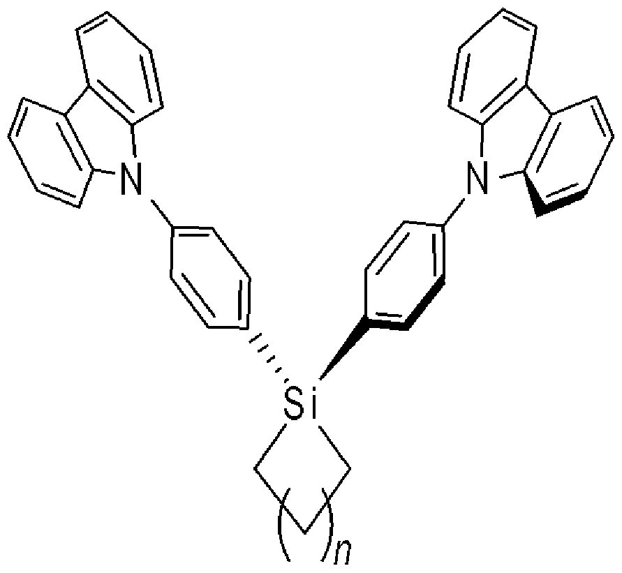
[34] Preferred specific examples of the compound capable for electrochemical deposition in the invention are as followings: [35]
Figure imgf000007_0001
[36]
Figure imgf000007_0002
[37] wherein n is an integer of 1 to 3, [38]
Figure imgf000008_0001
[39] wherein R is each independently a hydrogen atom or methyl, [40]
Figure imgf000008_0002
[41] wherein R is a methyl or phenyl, [42]
Figure imgf000008_0003
[43] wherein R is a methyl or phenyl, [44]
Figure imgf000009_0001
[45] wherein R is a methyl or phenyl, [46]
Figure imgf000009_0002
[47] wherein R is a methyl or phenyl, [48]
Figure imgf000009_0003
[49] wherein R is a methyl or phenyl, [50]
Figure imgf000010_0001
[51] wherein R is a methyl or phenyl, [52]
Figure imgf000010_0002
[53] As used herein, the term electrochemical deposition refers to a method of forming organic thin layers by putting substrates to be deposited into a reaction vessel where the above compounds forming the organic thin layers which are intended to deposit and electrolytes are dissolved and depositing the compounds intended to deposit onto the substrates to be deposited by application of power.
[54] The compounds forming the organic thin layers which are intended to deposit can be chosen among the above described compounds, depending on the organic thin layers to be formed on the substrates to be deposited, and the organic thin layer is one of the organic layers formed between anode and cathode and can be a hole injection layer (HIL), hole transport layer (HTL), emitting layer (EML), hole blocking layer (HBL), electron transport layer (ETL) or electron injection layer (EIL).
[55] Any solvents capable of dissolving the electrolytes and the compounds intended to deposit can be used in the above reaction vessel and as specific examples, there are dichloromethane (CH Cl ), tetrahydrofuran (THF), acetonitrile (CH CN), benzonitrile (C H CN), propylene carbonate (1,2-propanediol cycliccarbonate), and toluene (C H
6 5 6 5
CH ). In the case of forming the organic thin layers having two or more layers, however, it would be advisable to avoid the use of solvents capable of dissolving the compounds of the previously formed organic thin layers. The amount of the solvents to be used is preferably 0.01 to 10 mM on the basis of the concentration of the compounds. If the concentration is too thin, there is a possibility that the electrochemical deposition is not performed properly and if it is too thick, problems may happen in connection with the control of the electrochemical deposition film thickness and voltage drop.
[56] The electrolytes that can be used in the reaction vessel are dissolved in the above solvents and they are not limited to specific ones as long as they are able to ionize the compounds intended to deposit when power is applied, and as specific examples, there are Me NBF , Et NBF , Pr NBF , Bu NBF , Me NClO , Et NClO , Pr NClO , Bu NClO 4 , Me 4 NPF 6 , Et 4 NPF 6 , Pr 4 NPF 6 , Bu 4 NPF 6 , LiClO 4 , LiBF 4 , LiPF 6 , and LiBOB. The concentration of the supporting electrolytes is preferably 50 mM to 500 mM. If the concentration of the electrolytes is too thin, such problems as voltage drop may happen.
[57] As the substrates to be deposited in the invention, any conventional substrates used to form organic thin layers in OLED devices can be used. As specific examples, they can be a substrate with anode formed thereon; or a substrate on which anode and at least one layer from hole injection layer (HIL), hole transport layer (HTL), emitting layer (EML), hole blocking layer (HBL) and electron transport layer (ETL) are deposited in sequence.
[58] Any substrates used in common organic EL devices can be employed as the substrates and it is preferable to use organic substrates or clear plastic substrates with excellent clearness, surface flatness, easy handling and waterproof.
[59] Also, as anode forming materials, there can be used indium tin oxide (ITO), indium zinc oxide (IZO), tin oxide (SnO ), zinc oxide (ZnO), etc. that are clear and have excellent conductivity.
[60] The one or more organic layers among the hole injection layer (HIL), hole transport layer (HTL), emitting layer (EML), hole blocking layer (HBL) and electron transport layer (ETL) to be formed on the substrates to be deposited can be formed by known methods or by the electrochemical deposition of the invention. Preferably, the above organic layers are formed using the electrochemical deposition of the invention.
[61] Thereafter, on the organic thin layer formed by the electrochemical deposition can be further formed one or more organic thin layers through known organic layer formation methods or the electrochemical deposition of the invention and finally, organic light emitting devices are completed by depositing cathode on the formed organic thin layers. Likewise, the electrochemical deposition is preferably used to form the organic thin layers in this step.
[62] Of course, the cathode can be formed by any known methods and for example, the cathode can be formed by vacuum heat deposition of or sputtering metals for the formation of cathode. For the metals for the formation of cathode, there can be used lithium (Li), magnesium (Mg), aluminum (Al), aluminum-lithium (Al-Li), calcium (Ca), magnesium-indium (Mg-In), magnesium- silver (Mg-Ag) and the like. Furthermore, in case of obtaining front light emitting-type organic electroluminescence devices, clear substances such as ITO or IZO can be used as cathode.
[63] If necessary, in the invention, it is possible to further form one or more intermediate layers between the selected layers of the anode, hole injection layer (HIL), hole transport layer (HTL), emitting layer (EML), hole blocking layer (HBL), electron transport layer (ETL), electron injection layer (EIL) and cathode.
[64] The thickness of the organic thin layers formed through the electrochemical deposition in accordance with the present invention can be adjusted by power cycle control, depending on the required level and it is preferably 10 to 1,000 D and more preferably, 20 to 150 D. In the invention, power is applied preferably using CV (cyclic voltammetry). Voltage is applied in the range of voltage within potential window showing no oxidation-reduction of solvents or electrolytes or electrodes, and when CV is used, although there are slight variations in each compound, voltage is scanned starting from 0.30 V vs S.C.E. up to 1.65(+0.1) V vs S.C.E. at a voltage scan rate of 0.1 V/s and returned to 0.30 V vs S.C.E. at the same rate, which thus constitutes 1 cycle and preferably, several cycles are repeated. As the cycles are repeated and as current is increased, electrochemical deposition proceeds. The thickness of thin layers of compounds can be adjusted by varying the number of cycles, the concentration of the compounds, voltage scan rate, voltage scan range and so on. Of course, it is possible to carry out electrochemical deposition through the application of a poten- tiostatic voltage instead of cyclic voltammetry.
[65] Furthermore, after the formation of the organic thin layers through the electrochemical deposition of the present invention, washing step or dry step can be further carried out, if required. Through the washing step can be eliminated electrolyte substances that might be present on the organic thin layers, and those used as the solvent component of the reaction vessel are preferably used as the washing solution. The dry step is not limited to specific ones, and any known dry methods that can be carried out after the formation of known organic thin layers of organic light emitting devices can be applied.
[66] The method for preparing an organic thin layer of organic light emitting device using the electrochemical deposition of the present invention can be explained using the compound shown below (wherein R is methyl)
[67]
Figure imgf000013_0001
[68] First, prepare a reaction vessel where the above compound is dissolved in a solvent, dichlorormethane, together with an electrolyte, Bu NBF . The concentration of the compound of the above formula can be 0.5 mM and the concentration of the electrolyte can be 0.1 M. Thereafter, put a substrate to be deposited into the reaction vessel and then apply power. The substrate to be deposited can be a glass substrate with ITO as anode deposited thereon, a substrate of the glass substrate-ITO-hole injection layer being laminated in order, or a substrate of the glass substrate-ITO-hole injection layer- hole transport layer being laminated in order. Through the application of power, the compound dissolved in the reaction vessel is deposited onto the substrate to be deposited and the thickness to be deposited can be adjusted by the number of cycles of CV (cyclic voltammetry). After deposition, the substrate deposited with the above compound may be further deposited with one or more organic thin layers such as electron transport layer and electron injection layer, if necessary, after washing and dry and then, cathode is formed on the organic layers through vacuum heat deposition or sputtering, thereby completing an organic light emitting device.
[69] The method for preparation of the organic thin layer of organic light emitting device through electrochemical deposition according to the invention has simple process by virtue of the use of monomolecular compounds that are purchased or easily prepared without requiring special equipments, has high productivity, can make it easy to control the thickness of thin layers to be prepared and can fundamentally improve erosion of the pre-formed organic thin layers that occurred in the preparation of two or more organic thin layers by spin coating.
[70] Furthermore, the invention provides the organic thin layers of organic light emitting device prepared by the electrochemical deposition and organic light emitting devices comprising the organic thin layers as well. The organic thin layers have excellent adhesion to substrates, have uniform surface because their thickness can be adjusted at molecular level, and have excellent morphology stability and especially, in case of the organic thin layers formed through consecutive electrochemical deposition of two or more layers, interfaces between layers are even, erosion due to solvents does not occur, adhesion between interfaces is strong and they have fine patterns. Moreover, as the organic thin layers in accordance with the invention are not melted in most organic solvents, erosion due to solvents can be fundamentally reduced even in case of forming organic thin layers by known spin coating.
[71]
[72] For better understanding of the present invention, preferred embodiments follow.
The following examples are intended to merely illustrate the invention without limiting the scope of the invention.
[73]
[74] EXAMPLES
[75] All the works in the examples of the invention were done under nitrogen or argon atmosphere using standard Schlenk technology. Tetrahydrofuran (THF) was distilled using potassium benzophenone immediately before in use. IH and 13C NMRs were determined using Varian mercury 300 of 300.1 and 75.4 MHz. All the chemical shifts of hydrogen and carbon were determined using residual benzene of quenching solvent (99.5% CDCl ) on the basis of tetramethylsilane (Me Si). The element analysis was carried out using CHNS-O EA 1108 analyzer of Carlo Erba Co., Ltd. Fluorescent quantum yield was obtained through dilution methods on the basis of 9,10-diphenylanthracene. For the CV experiment, BAS 100 electrochemical analyzer was used. Three-electrode system - glassy carbon as a working electrode, platinum electric wire as a counter electrode and silver electric wire as a reference electrode - was used. Methylene chloride that is neat, distilled and degassed was used as a solvent and 0.1 M tetra-normal-butylammonium hexafluorophosphate was used as an electrolyte. Normal-butyllithium diluted in 1,4-dibromobenzene 2.5 M hexane was purchased from Aldrich Co., Ltd. and used without further purification.
[76] Synthesis 1
[77] Synthesis of 9,9'-bis(phenylcarbazol) derivatives containing silicon ring
(Compounds a-d)
[78] 9,9'-bis(phenylcarbazol) containing silicon ring (Compounds a-d) were synthesized in accordance with reaction formula 1 below. 1,4-dibromobenzene and carbazol were reacted using Ullmann's reaction to prepare Compound 1, to which normal- butyllithium and silanecyclodichloride were added and then reacted to synthesize 9,9'-bis(phenylcarbazol) derivative compounds a-d. However, in the case of 4-CBP compound a, ring coupling angle was unstable so quadrangular ring shortly became loose. All the 9,9'-bis(phenylcarbazol) derivatives containing silicon ring except for the quadrangle could be separated through columns with yields of 40-50%.
[79] [80] Synthesis of 9-(4-bromophenyl)carbazol (Compound a)
[81] Teflon magnetic stir bar, 1,4-dibromobenzene (25.184 g, 200 mmol), carbazol (8.36 g, 50 mmol), K CO (13.82 g, 100 mmol), and CuSO (7.98 g, 50 mmol) were put in a 100-mL one-neck flask and stirred at 210 0C for 16 hours without solvents. After the completion of the reaction, the mixture was diluted with methylenechloride and filtered and then, the filtered solution was washed with distilled water and brine. The thus obtained organic layer was dehydrated using MgSO .
[82] IH NMR (CDCl ): δ 8.21 (d, 2H), 7.40 (d, 2H), 7.25 (t, 2H), 7.13 (t, 2H), 7.35 (d,
2H), 7.16 (d, 2H) 13C NMR (CDC13): 111.1, 122.5, 125.7, 128.1, 130.2, 133.3
[83]
[84] Synthesis of 9,9'-bis(phenylcarbazole) containing pentagonal silicon ring
(Compound b)
[85] After 9-(4-bromophenyl)carbazole (1) (2.25 g, 12.5 mmol) was diluted in distilled tetrahydrofuran (THF) (10 mL), 2.5 M normal-butyllithium was dropwise added thereto at -78 0C. Stirring was carried out at the same temperature for 30 min and then dichlorocyclopentylsilane (2 mmol) was slowly dropwise added thereto. After the completion of dropwise addition, the reaction temperature was raised to room temperature and the mixture was stirred again for 3 hours. After the elimination of the solvents, the residuals were separated through silica gel column using ethylacetate/ hexane (volume ratio 1:10) as a developer and the yield was 43%.
[86] IH NMR (CDCl3): δ 8.055, 7.753, 7.320, 7.215 (m, 16H, Cz), 7.536, 7.408 (m, 8H,
Ph), 1.839 (m, 4H, CH2), 1.198 (t, 4Η, CH2). 13C NMR (CDCl ): 12.741, 28.158 (C Η2), 110.098, 120.265, 120.538, 123.695, 126.145, 126.555, 135.963, 136.464, 139.05, 140.811 (CH).
[87]
[88] Synthesis of 9,9'-bis(phenylcarbazole) containing silicon ring having pentagonal double bond (Compound c)
[89] This compound was synthesized in accordance with the same method as used for
Compound b above, using dichloropentenylsilane instead of dichlorocyclopentylsilane in synthesis of Compound b and separated with a yield of 47%.
[90] IH NMR (CDCl ): 8.152, 7.877, 7.414, 7.297 (m, 16H, Cz), 7.654, 7.501 (m, 8H,
Ph), 6.145 (m, H, CH2), 2.027 (d, 4Η, CH). 13C NMR (CDCl ): 0.359, 17.361 (CΗ2), 110.038, 120.265, 120.516, 123.672, 126.130, 126.600, 131.229, 134.787, 136.464, 140.743 (CH).
[91]
[92] Synthesis of 9,9'-bis(phenylcarbazole) containing silicon ring having hexagon
(Compound d)
[93] This compound was synthesized in accordance with the same method as used for Compound b above, using dichlorohexylsilane instead of dichlorocyclopentylsilane in synthesis of Compound b and separated with a yield of 50%.
[94] IH NMR (CDCl ): 8.125, 7.805, 7.380, 7.266 (m, 16H, Cz), 7.588, 7.474 (m, 8H, Ph), 1.890 (m, 4H, CH2), 1.614 (m, 2Η, CH2), 1.334 (t, 4Η, CH2). 13C NMR (CDCl ): 12.073, 24.789, 30.305 (CΗ2), 110.159, 120.273, 120.561, 123.710, 126.168, 126.585, 135.902, 136.236, 138.930, 140.81(CH).
[95] [96]
Figure imgf000016_0001
n = 1 ,1a n = 2s,i b n = 3s, ci n =2,dSi
[97] [Reaction formula 1] [98] [99] Synthesis 2 [100] Synthesis of mono-, bis-, tris-(9-phenylcarbazol) (Compounds 4-6), and 9-phenyl carbazol (7).
[101] Mono-, bis-, tris-(9-phenylcarbazol) (Compounds 4-6), and 9-phenyl carbazol (7) were prepared in accordance with reaction formula 2 below. Bromophenylcarbazol was converted into an organic lithium compound in tetrahydrofuran (THF) solvent using normal-butyllithium at -78 0C and then hydrogenated using water to synthesize 9-phenylcarbozol (Compound 7). Bromophenylcarbazol was converted into an organic lithium compound in tetrahydrofuran (THF) solvent using normal-butyllithium at -78 0C and then reacted with trichlorosilane, dimethyldichloridesilane, and trichloromethylsilane to synthesize mono-, bis-, tirs-(9-(phenylcarbozol)) (Compound 4-6), respectively with yields of 40-75%. Compound 5 and Compound 6 were separated through silica gel column and Compound 4 could be obtained by re- crystallization using ether without separation with column.
[102] [103] Synthesis of 9-(4-trimethylsilyl)phenyl)carbozol (Compound 4) [104] This compound was synthesized in accordance with the same method as used for
Compound b above, using trimethylchlorosilane instead of dichlorocyclopentylsilane in synthesis of Compound b and separated with a yield of 75%.
[105] IH NMR (CDCl ): 8.122, 7.719, 7.376, 7.262 (m, 8H, Cz), 7.527, 7.434 (m, 4H,
Ph), 0.348 (s, 9H, CfB), 13C NMR (CDCl ): -0.605 (CH3), 110.136, 120.136, 120.516, 123.619, 126.115, 126.396, 135.045, 138.360, 139.984, 140.955 (CH).
[106]
[107] Synthesis of bis(4-(carbatol-9-yl)phenyl)dimethylsilane (Compound 5)
[108] This compound was synthesized in accordance with the same method as used for
Compound b above, using dichlorodimethylsilane instead of dichlorocyclopentylsilane in synthesis of Compound b and separated with a yield of 60%.
[109] IH NMR (CDCl ): 8.148, 7.829, 7.409, 7.290 (m, 16H, Cz), 7.625, 7.492 (m, 8H,
Ph), 0.734 (s, 6H, CfB), 13C NMR (CDCl ): -1.842 (CH3), 110.068, 120.197, 120.500, 123.626, 126.100, 126.487, 135.879, 137.260, 138.854, 140.796 (CH).
[HO]
[111] Synthesis of 9,9',9"-(4,4',4"-(methylsilanetriyl)tris(4,l-phenyl))tris(carbazol) (Comp ound 6)
[112] This compound was synthesized in accordance with the same method as used for
Compound b above, using trichloromethylsilane instead of dichlorocyclopentylsilane in synthesis of Compound b and separated with a yield of 42%.
[113] IH NMR (CDCl ): 8.141, 7.897, 7.410, 7.288 (m, 24H, Cz), 7.683, 7.534 (m, 12H,
Ph), 1.086 (s, 3H, CfB), 13C NMR (CDC13): -2.600 (CH3), 110.129, 120.394, 120.607, 123.786, 126.214, 126.646, 134.795, 137.055, 193.430, 140.766 (CH).
[114]
[115] Synthesis of 9-phenylcarbazol (Compound 7)
[116] After 9-(4-bromophenyl)carbazole (1) (2.25 g, 12.5 mmol) was diluted in distilled tetrahydrofuran (THF) (10 ml), 2.5 M normal-butyllithium was dropwise added thereto -78 0C. At the same temperature, stirring proceeded for 30 min. and the reaction was terminated using distilled water. The organic layer was extracted using ether and hydrated using MgSO4. After the elimination of solvents, the residue was re- crystallized from the ether phase, affording 13.8 g of a white solid (yield 93%).
[117] IH NMR (CDCl ): 8.27 (d, 2H), 7.51 (d, 2H), 7.33 (t, 2H), 7.23 (t, 2H), 7.18 (d,
2H) 13C NMR (CDCl ): 111.8, 122.9, 125.7, 128.5, 130.8, 133.9
[118]
Figure imgf000018_0001
Figure imgf000018_0002
Figure imgf000018_0003
[119] [Reaction Formula 2] [120] [121] To examine the electrochemical properties and the HOMO and LUMO levels of Compounds b-d and Compounds 4-7 above, CV experiments were performed using Pt working electrode, Pt counter electrode, and Ag/Ag+(0.1M) electrode as reference electrode. CV was carried out with the variation of several measuring speeds by dissolving 0.1 M tetrabutylammoniumtetrafluoroborate (Bu 4 NBF 4 ) as an electrolyte in methylenechloride solvent and blowing nitrogen gas at room temperature. The measured values were examined on the basis of ferrocene. The electrochemical deposition using CV was carried out at a rate of 100 mV/s. First, the electrochemical properties of 9,9-bis(phenylcarbazol) derivatives containing silicon ring were investigated. In the course of analyzing the electrochemical properties, it was found that a certain amount of films were formed on the working electrode. In order to investigate conditions under which electrochemical deposition occurred, 1/2CBP (Compound 7) and Compounds 4, 5 and 6 were synthesized and CBP was purchased from Gracel Co., Ltd. and they were subject to CV tests under the same experimental conditions. The CV pictures of CBP derivatives (Compounds b-d and Compounds 4-7) linked with silicon and CBP are shown in Fig. 1 to Fig. 6.
[122] As seen in Fig. 1 to Fig. 6, the CBP derivatives other than 1/2 CBP all deposited electrochemically. Based on this experiment, it can be verified that at least two 9-phenylcarbazol derivatives are required for electrochemical deposition. Further, it could be verified that all the CBP derivatives linked with silicon have very similar electrochemical properties owing to silicon atom present in their center. Furthermore, as van der waals radius around the center silicon atom became small when electrochemical deposition occurred, and as the number of CBP derivatives to be substituted increased, electrochemical deposition could readily occur and the results are summarized in Table 1.
[123] Table 1
Figure imgf000019_0001
[124] •;*:• Platinum electrode used, the number of layers calculated on the basis of the fact that the monomolecular layer of 9,10-phenanthaquinone(PAQ) is 1.9x10 -10 mol PAQ/ cm
Industrial Applicability
[125] The method for preparation of the organic thin layer of organic light emitting device through electrochemical deposition according to the invention has simple process by virtue of the use of monomolecular compounds that are purchased or easily prepared without requiring special equipments, has high productivity, can make it easy to control the thickness of thin layers to be prepared and can fundamentally improve erosion of the pre-formed organic thin layers that occurred in the preparation of two or more organic thin layers by spin coating. Furthermore, the organic thin layers in accordance with the invention have excellent adhesion to substrates, have uniform surface because their thickness can be adjusted at molecular level, and have excellent morphology stability and especially, in case of the organic thin layers formed through consecutive electrochemical deposition of two or more layers, interfaces between layers are even, erosion due to solvents does not occur, adhesion between interfaces is strong and they have fine patterns. Moreover, as they are not melted in most organic solvents, erosion due to solvents can be fundamentally reduced even in case of forming organic thin layers by known spin coating on the organic thin layers in accordance with the invention.

Claims

Claims
[1] A method for preparing an organic thin layer of organic light emitting device comprising one or more organic thin layers between anode and cathode, characterized in that the organic thin layer is formed by electrochemical deposition of a compound having bis(phenylcarbazol) group in molecule.
[2] The method for preparing the organic thin layer of organic light emitting device according to claim 1, wherein the compound is represented by formula 1: [formula 1]
Figure imgf000021_0001
wherein X is a divalent linking group.
[3] The method for preparing the organic thin layer of organic light emitting device according to claim 2, wherein the linking group is -SiR 2 R 3 -, -PR 4 -, -NR 5 -, -O-, -
S-, -CR 6 R 7 - or a substituted or unsubstituted aryl group of C -C , and R to R
50 are each independently a substituted or unsubstituted alkyl group of C -C , substituted or unsubstituted aryl group of C -C , substituted or unsubstituted
J 6 50 hetero ring group of C -C , or substituted or unsubstituted heterocyclic ring
6 50 g °roup of C 6 -C 50.
[4] The method for preparing the organic thin layer of organic light emitting device according to claim 3, wherein the linking group is -SiR R -, and R to R are each independently a substituted or unsubstituted alkyl group of C -C , substituted or unsubstituted aryl group of C -C , substituted or unsubstituted hetero ring group of C -C , or substituted or unsubstituted heterocyclic ring group of C -C .
6 50 J & & r 6 50
[5] The method for preparing the organic thin layer of organic light emitting device according to claim 1, wherein the compound is selected from the following:
Figure imgf000021_0002
Figure imgf000022_0001
wherein n is an integer of 1 to 3,
Figure imgf000022_0002
wherein R is each independently a hydrogen atom or methyl,
Figure imgf000022_0003
wherein R is a methyl or phenyl,
Figure imgf000023_0001
wherein R is a methyl or phenyl,
Figure imgf000023_0003
wherein R is a methyl or phenyl,
Figure imgf000024_0001
wherein R is a methyl or phenyl,
Figure imgf000024_0002
wherein R is a methyl or phenyl, and
Figure imgf000024_0003
[6] The method for preparing the organic thin layer of organic light emitting device according to claim 1, wherein the organic thin layer is a hole injection layer (HIL), hole transport layer (HTL), emitting layer (EML), hole blocking layer (HBL), electron transport layer (ETL) or electron injection layer (EIL).
[7] The method for preparing the organic thin layer of organic light emitting device according to claim 1, wherein a solvent which is dichloromethane (CH Cl ),
2 tetrahydrofuran (THF), acetonitrile (CH CN) or benzonitrile (C H CN),
3 6 5 propylene carbonate (1,2-propanediol cycliccarbonate), or toluene (C H CH ) is
6 5 3 used in the electrochemical deposition.
[8] The method for preparing the organic thin layer of organic light emitting device according to claim 1, wherein one or more electrolytes selected from the group consisting of Me NBF , Et NBF , Pr NBF , Bu NBF , Me NClO , Et NClO , Pr NClO , Bu NClO , Me NPF , Et NPF , Pr NPF , Bu NPF , LiClO , LiBF , LiPF ,
4 4 4 4 6 4 6 4 6 4 6 4 4 6 and LiBOB are used in the electrochemical deposition. [9] An organic thin layer of organic light emitting device prepared by the method as described in any one of claims 1 to 8. [10] An organic light emitting device comprising at least one organic thin layer between anode and cathode, characterized in that it comprises at least one or ganic thin layer as described in claim 9. [11] The organic light emitting device according to claim 10 wherein the organic light emitting device comprises consecutive two or more organic thin layers as described in claim 9. [12] A display device comprising the organic light emitting device as described in claim 10.
PCT/KR2007/001721 2006-04-14 2007-04-10 Preparing method for organic thin layer of organic light emitting devices using electrochemical deposition Ceased WO2007119954A1 (en)

Priority Applications (2)

Application Number Priority Date Filing Date Title
JP2009505292A JP5113153B2 (en) 2006-04-14 2007-04-10 Method for forming organic thin film layer of organic light emitting device by electrochemical deposition
DE112007000924T DE112007000924T5 (en) 2006-04-14 2007-04-10 Method for producing an organic thin film of organic light-emitting devices by means of electrochemical deposition

Applications Claiming Priority (2)

Application Number Priority Date Filing Date Title
KR1020060034296A KR101299098B1 (en) 2006-04-14 2006-04-14 Preparing method for organic thin layer of organic light emitting devices using electrochemical deposition
KR10-2006-0034296 2006-04-14

Publications (1)

Publication Number Publication Date
WO2007119954A1 true WO2007119954A1 (en) 2007-10-25

Family

ID=38609689

Family Applications (1)

Application Number Title Priority Date Filing Date
PCT/KR2007/001721 Ceased WO2007119954A1 (en) 2006-04-14 2007-04-10 Preparing method for organic thin layer of organic light emitting devices using electrochemical deposition

Country Status (4)

Country Link
JP (1) JP5113153B2 (en)
KR (1) KR101299098B1 (en)
DE (1) DE112007000924T5 (en)
WO (1) WO2007119954A1 (en)

Cited By (1)

* Cited by examiner, † Cited by third party
Publication number Priority date Publication date Assignee Title
CN103881067A (en) * 2012-12-24 2014-06-25 海洋王照明科技股份有限公司 Polymer blue-light main material, and preparation method and application thereof

Families Citing this family (6)

* Cited by examiner, † Cited by third party
Publication number Priority date Publication date Assignee Title
KR101352021B1 (en) * 2006-05-17 2014-01-15 주식회사 동진쎄미켐 Silicon type compound having bisphenylcarbazol in element and method for preparing of organic thin layer of organic light emitting devices using it
DE102012217574A1 (en) * 2012-09-27 2014-03-27 Siemens Aktiengesellschaft Phosphoroxo salts as n-dopants for organic electronics
KR102167045B1 (en) * 2013-12-17 2020-10-19 삼성디스플레이 주식회사 Silane-based compounds and organic light emitting devices comprising the same
KR101612319B1 (en) 2014-08-28 2016-04-15 주식회사 네패스 Cyan Host Compound and Organic emitting Device Employing The Same
KR101775891B1 (en) 2014-12-23 2017-09-12 주식회사 네패스 Nitrogen hetero ring compound and organic emitting device employing the same
CN107275521A (en) * 2017-05-24 2017-10-20 华南理工大学 A kind of preparation method and applications of high-resolution array organic film

Citations (4)

* Cited by examiner, † Cited by third party
Publication number Priority date Publication date Assignee Title
JPH10168443A (en) * 1996-12-17 1998-06-23 Sanyo Shinku Kogyo Kk Phenylcarbazole derivative used for hole or electron transport layer of organic luminescent element
JP2002008860A (en) * 2000-04-18 2002-01-11 Mitsubishi Chemicals Corp Organic electroluminescent device
US6653654B1 (en) * 2002-05-01 2003-11-25 The University Of Hong Kong Electroluminescent materials
EP1480281A2 (en) * 2003-05-22 2004-11-24 Samsung SDI Co., Ltd. Electroluminescent display device

Family Cites Families (3)

* Cited by examiner, † Cited by third party
Publication number Priority date Publication date Assignee Title
JPH0845668A (en) * 1994-07-27 1996-02-16 Casio Comput Co Ltd Method for manufacturing electroluminescent device
JPH0997679A (en) * 1995-09-28 1997-04-08 Casio Comput Co Ltd Method for manufacturing electroluminescent device
KR100522697B1 (en) * 2003-09-22 2005-10-20 삼성에스디아이 주식회사 4,4'-Bis(carbazol-9-yl)-biphenyl based silicone compound and organic electroluminescence display device

Patent Citations (4)

* Cited by examiner, † Cited by third party
Publication number Priority date Publication date Assignee Title
JPH10168443A (en) * 1996-12-17 1998-06-23 Sanyo Shinku Kogyo Kk Phenylcarbazole derivative used for hole or electron transport layer of organic luminescent element
JP2002008860A (en) * 2000-04-18 2002-01-11 Mitsubishi Chemicals Corp Organic electroluminescent device
US6653654B1 (en) * 2002-05-01 2003-11-25 The University Of Hong Kong Electroluminescent materials
EP1480281A2 (en) * 2003-05-22 2004-11-24 Samsung SDI Co., Ltd. Electroluminescent display device

Cited By (1)

* Cited by examiner, † Cited by third party
Publication number Priority date Publication date Assignee Title
CN103881067A (en) * 2012-12-24 2014-06-25 海洋王照明科技股份有限公司 Polymer blue-light main material, and preparation method and application thereof

Also Published As

Publication number Publication date
JP5113153B2 (en) 2013-01-09
KR20070102305A (en) 2007-10-18
DE112007000924T5 (en) 2009-09-03
JP2009533816A (en) 2009-09-17
KR101299098B1 (en) 2013-08-28

Similar Documents

Publication Publication Date Title
JP5281270B2 (en) Iridium complex compound, organic electroluminescence device using the same, and use thereof
KR101434632B1 (en) Arylamine compounds and electronic devices
KR100611885B1 (en) Organometallic compound in which a host compound and a dopant compound are connected, an organic electroluminescent device using the same, and a manufacturing method thereof
WO2007119954A1 (en) Preparing method for organic thin layer of organic light emitting devices using electrochemical deposition
CN107382926B (en) Compound and organic electronic device thereof
JP2013509390A (en) Novel compounds for electronic materials and organic electronic devices using the same
CN105764876A (en) Organic electroluminescent compound and organic electroluminescent device comprising said compound
WO2019143153A1 (en) Novel compound and organic light emitting device using same
KR20110086043A (en) Host Materials for Light Emitting Diodes
EP4230630B1 (en) Novel compound and organic light emitting device comprising the same
JP2023547680A (en) Novel compounds and organic light-emitting devices using them
JPWO2006070817A1 (en) Organic boron π-electron compounds and synthetic intermediates thereof
WO2019093623A1 (en) Novel heterocyclic compound and organic light-emitting diode using same
CN108864195A (en) A kind of metal iridium complex and its organic luminescent device
WO2007132986A1 (en) Silicon type compound having bisphenylcarbazol in molecule and method for preparing organic thin layer of organic light emitting devices using the same
JP7334886B2 (en) Novel compound and organic light-emitting device using the same
CN106939024A (en) A kind of tetradentate ligandses Pt complex compounds of unit based on miscellaneous nitrogen fluorenes for OLED material
KR20190082236A (en) Polymeric charge transport layer and organic electronic device comprising same
CN103261158B (en) N-Cycloalkylalkyltricarbazole
EP4293030A1 (en) Novel compound and organic light-emitting device using same
CN109311922A (en) Iridium complex and organic light-emitting element using same
KR20070111189A (en) Organic thin film formation method of organic light emitting device by electrochemical deposition
EP4279492A1 (en) Novel compound and organic light emitting device comprising same
KR101180159B1 (en) The New Host Materials for Blue Phosphorescent Emitter and Organic Light-Emitting Diodes Using This
KR101386217B1 (en) Calixarene-based compound and an organic light emitting device employing the same

Legal Events

Date Code Title Description
DPE2 Request for preliminary examination filed before expiration of 19th month from priority date (pct application filed from 20040101)
121 Ep: the epo has been informed by wipo that ep was designated in this application

Ref document number: 07745884

Country of ref document: EP

Kind code of ref document: A1

WWE Wipo information: entry into national phase

Ref document number: 2009505292

Country of ref document: JP

WWE Wipo information: entry into national phase

Ref document number: 1120070009241

Country of ref document: DE

122 Ep: pct application non-entry in european phase

Ref document number: 07745884

Country of ref document: EP

Kind code of ref document: A1

RET De translation (de og part 6b)

Ref document number: 112007000924

Country of ref document: DE

Date of ref document: 20090903

Kind code of ref document: P