WO2007011627A1 - Semiconductor device including a strained superlattice layer above a stress layer and associated methods - Google Patents
Semiconductor device including a strained superlattice layer above a stress layer and associated methods Download PDFInfo
- Publication number
- WO2007011627A1 WO2007011627A1 PCT/US2006/027119 US2006027119W WO2007011627A1 WO 2007011627 A1 WO2007011627 A1 WO 2007011627A1 US 2006027119 W US2006027119 W US 2006027119W WO 2007011627 A1 WO2007011627 A1 WO 2007011627A1
- Authority
- WO
- WIPO (PCT)
- Prior art keywords
- semiconductor
- layer
- graded
- semiconductor device
- superlattice
- Prior art date
Links
- 239000004065 semiconductor Substances 0.000 title claims abstract description 216
- 238000000034 method Methods 0.000 title claims description 31
- 239000010410 layer Substances 0.000 claims abstract description 243
- 239000002356 single layer Substances 0.000 claims abstract description 38
- 239000013078 crystal Substances 0.000 claims abstract description 11
- QVGXLLKOCUKJST-UHFFFAOYSA-N atomic oxygen Chemical compound [O] QVGXLLKOCUKJST-UHFFFAOYSA-N 0.000 claims description 18
- 239000001301 oxygen Substances 0.000 claims description 18
- 229910052760 oxygen Inorganic materials 0.000 claims description 18
- 229910000577 Silicon-germanium Inorganic materials 0.000 claims description 14
- LEVVHYCKPQWKOP-UHFFFAOYSA-N [Si].[Ge] Chemical compound [Si].[Ge] LEVVHYCKPQWKOP-UHFFFAOYSA-N 0.000 claims description 14
- 239000002800 charge carrier Substances 0.000 claims description 13
- IJGRMHOSHXDMSA-UHFFFAOYSA-N Atomic nitrogen Chemical compound N#N IJGRMHOSHXDMSA-UHFFFAOYSA-N 0.000 claims description 12
- 230000001939 inductive effect Effects 0.000 claims description 10
- 239000000758 substrate Substances 0.000 claims description 9
- 229910052757 nitrogen Inorganic materials 0.000 claims description 6
- PXGOKWXKJXAPGV-UHFFFAOYSA-N Fluorine Chemical compound FF PXGOKWXKJXAPGV-UHFFFAOYSA-N 0.000 claims description 5
- 229910052731 fluorine Inorganic materials 0.000 claims description 5
- 239000011737 fluorine Substances 0.000 claims description 5
- CSJDCSCTVDEHRN-UHFFFAOYSA-N methane;molecular oxygen Chemical compound C.O=O CSJDCSCTVDEHRN-UHFFFAOYSA-N 0.000 claims description 5
- XUIMIQQOPSSXEZ-UHFFFAOYSA-N Silicon Chemical compound [Si] XUIMIQQOPSSXEZ-UHFFFAOYSA-N 0.000 description 44
- 239000000463 material Substances 0.000 description 41
- 229910052710 silicon Inorganic materials 0.000 description 41
- 239000010703 silicon Substances 0.000 description 41
- 230000037230 mobility Effects 0.000 description 21
- 230000004888 barrier function Effects 0.000 description 6
- 230000000051 modifying effect Effects 0.000 description 6
- 229910052581 Si3N4 Inorganic materials 0.000 description 5
- 238000000151 deposition Methods 0.000 description 5
- 230000008021 deposition Effects 0.000 description 5
- HQVNEWCFYHHQES-UHFFFAOYSA-N silicon nitride Chemical compound N12[Si]34N5[Si]62N3[Si]51N64 HQVNEWCFYHHQES-UHFFFAOYSA-N 0.000 description 5
- VYPSYNLAJGMNEJ-UHFFFAOYSA-N Silicium dioxide Chemical compound O=[Si]=O VYPSYNLAJGMNEJ-UHFFFAOYSA-N 0.000 description 4
- 230000008901 benefit Effects 0.000 description 4
- 239000012212 insulator Substances 0.000 description 4
- 239000000203 mixture Substances 0.000 description 4
- 238000003775 Density Functional Theory Methods 0.000 description 3
- 230000007547 defect Effects 0.000 description 3
- 238000010586 diagram Methods 0.000 description 3
- 239000002019 doping agent Substances 0.000 description 3
- 238000009413 insulation Methods 0.000 description 3
- 238000012545 processing Methods 0.000 description 3
- OKTJSMMVPCPJKN-UHFFFAOYSA-N Carbon Chemical compound [C] OKTJSMMVPCPJKN-UHFFFAOYSA-N 0.000 description 2
- OBNDGIHQAIXEAO-UHFFFAOYSA-N [O].[Si] Chemical compound [O].[Si] OBNDGIHQAIXEAO-UHFFFAOYSA-N 0.000 description 2
- 125000004429 atom Chemical group 0.000 description 2
- 238000004364 calculation method Methods 0.000 description 2
- 229910052799 carbon Inorganic materials 0.000 description 2
- 229910052681 coesite Inorganic materials 0.000 description 2
- 150000001875 compounds Chemical class 0.000 description 2
- 229910052906 cristobalite Inorganic materials 0.000 description 2
- 238000013461 design Methods 0.000 description 2
- 239000003989 dielectric material Substances 0.000 description 2
- 230000006872 improvement Effects 0.000 description 2
- 238000004518 low pressure chemical vapour deposition Methods 0.000 description 2
- 238000004519 manufacturing process Methods 0.000 description 2
- 238000012986 modification Methods 0.000 description 2
- 230000004048 modification Effects 0.000 description 2
- 239000002052 molecular layer Substances 0.000 description 2
- 230000003287 optical effect Effects 0.000 description 2
- 230000005693 optoelectronics Effects 0.000 description 2
- 238000000623 plasma-assisted chemical vapour deposition Methods 0.000 description 2
- 230000008569 process Effects 0.000 description 2
- 238000000926 separation method Methods 0.000 description 2
- 239000000377 silicon dioxide Substances 0.000 description 2
- LIVNPJMFVYWSIS-UHFFFAOYSA-N silicon monoxide Chemical class [Si-]#[O+] LIVNPJMFVYWSIS-UHFFFAOYSA-N 0.000 description 2
- 229910052682 stishovite Inorganic materials 0.000 description 2
- 229910052905 tridymite Inorganic materials 0.000 description 2
- 241001496863 Candelaria Species 0.000 description 1
- 206010010144 Completed suicide Diseases 0.000 description 1
- UFHFLCQGNIYNRP-UHFFFAOYSA-N Hydrogen Chemical compound [H][H] UFHFLCQGNIYNRP-UHFFFAOYSA-N 0.000 description 1
- 229910000676 Si alloy Inorganic materials 0.000 description 1
- 229910008310 Si—Ge Inorganic materials 0.000 description 1
- 239000002099 adlayer Substances 0.000 description 1
- 229910045601 alloy Inorganic materials 0.000 description 1
- 239000000956 alloy Substances 0.000 description 1
- 238000000137 annealing Methods 0.000 description 1
- 229910052787 antimony Inorganic materials 0.000 description 1
- WATWJIUSRGPENY-UHFFFAOYSA-N antimony atom Chemical compound [Sb] WATWJIUSRGPENY-UHFFFAOYSA-N 0.000 description 1
- 229910052785 arsenic Inorganic materials 0.000 description 1
- RQNWIZPPADIBDY-UHFFFAOYSA-N arsenic atom Chemical compound [As] RQNWIZPPADIBDY-UHFFFAOYSA-N 0.000 description 1
- 238000000231 atomic layer deposition Methods 0.000 description 1
- 230000009286 beneficial effect Effects 0.000 description 1
- 230000000903 blocking effect Effects 0.000 description 1
- 230000015556 catabolic process Effects 0.000 description 1
- 238000012937 correction Methods 0.000 description 1
- 235000021438 curry Nutrition 0.000 description 1
- 238000006731 degradation reaction Methods 0.000 description 1
- 238000009826 distribution Methods 0.000 description 1
- 230000000694 effects Effects 0.000 description 1
- 230000005684 electric field Effects 0.000 description 1
- 238000005516 engineering process Methods 0.000 description 1
- 230000002708 enhancing effect Effects 0.000 description 1
- 238000005530 etching Methods 0.000 description 1
- 229910052732 germanium Inorganic materials 0.000 description 1
- GNPVGFCGXDBREM-UHFFFAOYSA-N germanium atom Chemical compound [Ge] GNPVGFCGXDBREM-UHFFFAOYSA-N 0.000 description 1
- BHEPBYXIRTUNPN-UHFFFAOYSA-N hydridophosphorus(.) (triplet) Chemical compound [PH] BHEPBYXIRTUNPN-UHFFFAOYSA-N 0.000 description 1
- 239000001257 hydrogen Substances 0.000 description 1
- 229910052739 hydrogen Inorganic materials 0.000 description 1
- 238000002513 implantation Methods 0.000 description 1
- 238000007734 materials engineering Methods 0.000 description 1
- 239000011159 matrix material Substances 0.000 description 1
- 229910052751 metal Inorganic materials 0.000 description 1
- 239000002184 metal Substances 0.000 description 1
- 239000002086 nanomaterial Substances 0.000 description 1
- 150000004767 nitrides Chemical class 0.000 description 1
- 125000004430 oxygen atom Chemical group O* 0.000 description 1
- 230000035699 permeability Effects 0.000 description 1
- 238000012552 review Methods 0.000 description 1
- 229910052814 silicon oxide Inorganic materials 0.000 description 1
- 125000006850 spacer group Chemical group 0.000 description 1
- 241000894007 species Species 0.000 description 1
- 239000000126 substance Substances 0.000 description 1
- 230000007704 transition Effects 0.000 description 1
- 230000005641 tunneling Effects 0.000 description 1
- 230000005428 wave function Effects 0.000 description 1
Classifications
-
- H—ELECTRICITY
- H01—ELECTRIC ELEMENTS
- H01L—SEMICONDUCTOR DEVICES NOT COVERED BY CLASS H10
- H01L29/00—Semiconductor devices specially adapted for rectifying, amplifying, oscillating or switching and having potential barriers; Capacitors or resistors having potential barriers, e.g. a PN-junction depletion layer or carrier concentration layer; Details of semiconductor bodies or of electrodes thereof ; Multistep manufacturing processes therefor
- H01L29/02—Semiconductor bodies ; Multistep manufacturing processes therefor
- H01L29/06—Semiconductor bodies ; Multistep manufacturing processes therefor characterised by their shape; characterised by the shapes, relative sizes, or dispositions of the semiconductor regions ; characterised by the concentration or distribution of impurities within semiconductor regions
- H01L29/10—Semiconductor bodies ; Multistep manufacturing processes therefor characterised by their shape; characterised by the shapes, relative sizes, or dispositions of the semiconductor regions ; characterised by the concentration or distribution of impurities within semiconductor regions with semiconductor regions connected to an electrode not carrying current to be rectified, amplified or switched and such electrode being part of a semiconductor device which comprises three or more electrodes
- H01L29/107—Substrate region of field-effect devices
- H01L29/1075—Substrate region of field-effect devices of field-effect transistors
- H01L29/1079—Substrate region of field-effect devices of field-effect transistors with insulated gate
- H01L29/1083—Substrate region of field-effect devices of field-effect transistors with insulated gate with an inactive supplementary region, e.g. for preventing punch-through, improving capacity effect or leakage current
-
- B—PERFORMING OPERATIONS; TRANSPORTING
- B82—NANOTECHNOLOGY
- B82Y—SPECIFIC USES OR APPLICATIONS OF NANOSTRUCTURES; MEASUREMENT OR ANALYSIS OF NANOSTRUCTURES; MANUFACTURE OR TREATMENT OF NANOSTRUCTURES
- B82Y10/00—Nanotechnology for information processing, storage or transmission, e.g. quantum computing or single electron logic
-
- H—ELECTRICITY
- H01—ELECTRIC ELEMENTS
- H01L—SEMICONDUCTOR DEVICES NOT COVERED BY CLASS H10
- H01L29/00—Semiconductor devices specially adapted for rectifying, amplifying, oscillating or switching and having potential barriers; Capacitors or resistors having potential barriers, e.g. a PN-junction depletion layer or carrier concentration layer; Details of semiconductor bodies or of electrodes thereof ; Multistep manufacturing processes therefor
- H01L29/02—Semiconductor bodies ; Multistep manufacturing processes therefor
- H01L29/06—Semiconductor bodies ; Multistep manufacturing processes therefor characterised by their shape; characterised by the shapes, relative sizes, or dispositions of the semiconductor regions ; characterised by the concentration or distribution of impurities within semiconductor regions
- H01L29/10—Semiconductor bodies ; Multistep manufacturing processes therefor characterised by their shape; characterised by the shapes, relative sizes, or dispositions of the semiconductor regions ; characterised by the concentration or distribution of impurities within semiconductor regions with semiconductor regions connected to an electrode not carrying current to be rectified, amplified or switched and such electrode being part of a semiconductor device which comprises three or more electrodes
- H01L29/1025—Channel region of field-effect devices
- H01L29/1029—Channel region of field-effect devices of field-effect transistors
- H01L29/1033—Channel region of field-effect devices of field-effect transistors with insulated gate, e.g. characterised by the length, the width, the geometric contour or the doping structure
- H01L29/1054—Channel region of field-effect devices of field-effect transistors with insulated gate, e.g. characterised by the length, the width, the geometric contour or the doping structure with a variation of the composition, e.g. channel with strained layer for increasing the mobility
-
- H—ELECTRICITY
- H01—ELECTRIC ELEMENTS
- H01L—SEMICONDUCTOR DEVICES NOT COVERED BY CLASS H10
- H01L29/00—Semiconductor devices specially adapted for rectifying, amplifying, oscillating or switching and having potential barriers; Capacitors or resistors having potential barriers, e.g. a PN-junction depletion layer or carrier concentration layer; Details of semiconductor bodies or of electrodes thereof ; Multistep manufacturing processes therefor
- H01L29/02—Semiconductor bodies ; Multistep manufacturing processes therefor
- H01L29/12—Semiconductor bodies ; Multistep manufacturing processes therefor characterised by the materials of which they are formed
- H01L29/15—Structures with periodic or quasi periodic potential variation, e.g. multiple quantum wells, superlattices
- H01L29/151—Compositional structures
-
- H—ELECTRICITY
- H01—ELECTRIC ELEMENTS
- H01L—SEMICONDUCTOR DEVICES NOT COVERED BY CLASS H10
- H01L29/00—Semiconductor devices specially adapted for rectifying, amplifying, oscillating or switching and having potential barriers; Capacitors or resistors having potential barriers, e.g. a PN-junction depletion layer or carrier concentration layer; Details of semiconductor bodies or of electrodes thereof ; Multistep manufacturing processes therefor
- H01L29/66—Types of semiconductor device ; Multistep manufacturing processes therefor
- H01L29/68—Types of semiconductor device ; Multistep manufacturing processes therefor controllable by only the electric current supplied, or only the electric potential applied, to an electrode which does not carry the current to be rectified, amplified or switched
- H01L29/76—Unipolar devices, e.g. field effect transistors
- H01L29/772—Field effect transistors
- H01L29/78—Field effect transistors with field effect produced by an insulated gate
- H01L29/7833—Field effect transistors with field effect produced by an insulated gate with lightly doped drain or source extension, e.g. LDD MOSFET's; DDD MOSFET's
-
- H—ELECTRICITY
- H01—ELECTRIC ELEMENTS
- H01L—SEMICONDUCTOR DEVICES NOT COVERED BY CLASS H10
- H01L21/00—Processes or apparatus adapted for the manufacture or treatment of semiconductor or solid state devices or of parts thereof
- H01L21/70—Manufacture or treatment of devices consisting of a plurality of solid state components formed in or on a common substrate or of parts thereof; Manufacture of integrated circuit devices or of parts thereof
- H01L21/77—Manufacture or treatment of devices consisting of a plurality of solid state components or integrated circuits formed in, or on, a common substrate
- H01L21/78—Manufacture or treatment of devices consisting of a plurality of solid state components or integrated circuits formed in, or on, a common substrate with subsequent division of the substrate into plural individual devices
- H01L21/82—Manufacture or treatment of devices consisting of a plurality of solid state components or integrated circuits formed in, or on, a common substrate with subsequent division of the substrate into plural individual devices to produce devices, e.g. integrated circuits, each consisting of a plurality of components
- H01L21/822—Manufacture or treatment of devices consisting of a plurality of solid state components or integrated circuits formed in, or on, a common substrate with subsequent division of the substrate into plural individual devices to produce devices, e.g. integrated circuits, each consisting of a plurality of components the substrate being a semiconductor, using silicon technology
- H01L21/8232—Field-effect technology
- H01L21/8234—MIS technology, i.e. integration processes of field effect transistors of the conductor-insulator-semiconductor type
- H01L21/8238—Complementary field-effect transistors, e.g. CMOS
- H01L21/823807—Complementary field-effect transistors, e.g. CMOS with a particular manufacturing method of the channel structures, e.g. channel implants, halo or pocket implants, or channel materials
Definitions
- the present invention relates to the field of semiconductors, and, more particularly, to semiconductors having enhanced properties based upon energy band engineering and associated methods.
- 6,472,685 B2 to Takagi discloses a semiconductor device including a silicon and carbon layer sandwiched between silicon layers so that the conduction band and valence band of the second silicon layer receive a tensile strain. Electrons having a smaller effective mass, and which have been induced by an electric field applied to the gate electrode, are confined in the second silicon layer, thus, an n-channel MOSFET is asserted to have a higher mobility.
- U.S. Patent No. 4,937,204 to Ishibashi et al discloses a superlattice in which a plurality of layers, less than eight monolayers, and containing a fraction or a binary compound semiconductor layers, are alternately and epitaxially grown.
- U.S. Patent No. 5,357,119 to Wang et al discloses a Si-Ge short period superlattice with higher mobility achieved by reducing alloy scattering in the superlattice.
- U.S. Patent No. 5,683,934 to Candelaria discloses an enhanced mobility MOSFET including a channel layer comprising an alloy of silicon and a second material substitutional ⁇ present in the silicon lattice at a percentage that places the channel layer under tensile stress.
- U.S. Patent No. 5,216,262 to Tsu discloses a quantum well structure comprising two barrier regions and a thin epitaxially grown semiconductor layer sandwiched between the barriers. Each barrier region consists of alternate layers of SiO 2 /Si with a thickness generally in a range of two to six monolayers. A much thicker section of silicon is sandwiched between the barriers.
- An article entitled "Phenomena in silicon nanostructure devices" also to Tsu and published online September 6, 2000 by Applied Physics and Materials Science & Processing, pp. 391-402 discloses a semiconductor-atomic superlattice (SAS) of silicon and oxygen. The Si/O superlattice is disclosed as useful in a silicon quantum and light-emitting devices.
- SAS semiconductor-atomic superlattice
- a green electromuminescence diode structure was constructed and tested. Current flow in the diode structure is vertical, that is, perpendicular to the layers of the SAS.
- the disclosed SAS may include semiconductor layers separated by adsorbed species such as oxygen atoms, and CO molecules. The silicon growth beyond the adsorbed monolayer of oxygen is described as epitaxial with a fairly low defect density.
- One SAS structure included a 1.1 nm thick silicon portion that is about -eight atomic layers of silicon, and another structure had twice this thickness of silicon.
- the application discloses that material parameters, for example, the location of band minima, effective mass, etc., can be tailored to yield new aperiodic materials with desirable band-structure characteristics.
- Other parameters such as electrical conductivity, thermal conductivity and dielectric permittivity or magnetic permeability are disclosed as also possible to be designed into the material.
- a semiconductor device which may include a stress layer and a strained superlattice layer above the stress layer and comprising a plurality of stacked groups of layers. More particularly, each group of layers of the strained superlattice layer may include a plurality of stacked base semiconductor monolayers defining a base semiconductor portion, and at least one non-semiconductor monolayer constrained within a crystal lattice of adjacent base semiconductor portions.
- the stress layer may be a graded semiconductor layer, for example.
- the graded semiconductor layer may be graded in a vertical direction, and the strained superlattice may be vertically stacked on the graded semiconductor layer.
- the semiconductor device may further include a substantially ungraded semiconductor layer positioned between the graded semiconductor layer and the strained superlattice layer.
- the stress layer may include graded silicon germanium.
- the stress layer may also include a plurality of strain inducing pillars arranged in side-by-side relation.
- An insulating layer may also be positioned between the stress layer and the strained superlattice layer.
- the semiconductor device may further include regions for causing transport of charge carriers through the strained superlattice layer in a parallel direction relative to the stacked groups of layers .
- a semiconductor substrate may be adjacent the stress layer on a side thereof opposite the strained superlattice layer.
- the strained superlattice layer may have a compressive or tensile strain.
- the strained superlattice layer may also have a common energy band structure therein.
- each base semiconductor portion may include a base semiconductor selected from the group consisting of Group IV semiconductors, Group III-V semiconductors, and Group II- VI semiconductors. More particularly, each base semiconductor portion may include silicon.
- each non-semiconductor monolayer may include a non- semiconductor selected from the group consisting of oxygen, nitrogen, fluorine, and carbon-oxygen.
- Adjacent base semiconductor portions of the strained superlattice layer may be chemically bound together.
- each non-semiconductor monolayer may be a single monolayer thick, and each base semiconductor portion may be less than eight monolayers thick.
- the strained superlattice layer may further include a substantially direct energy bandgap.
- the strained superlattice layer may also include a base semiconductor cap layer on an uppermost group of layers. In some embodiments, all of the base semiconductor portions may be a same number of monolayers thick. Alternatively, at least some of the base semiconductor portions may be a different number of monolayers thick.
- a method aspect of the invention is directed to making a semiconductor device . The method may include forming a stress layer, and forming a strained superlattice layer above the stress layer and comprising a plurality of stacked groups of layers.
- FIG. 1 is a schematic cross-sectional view of a semiconductor device in accordance with the present invention including a stress layer and a strained superlattice above the stress layer.
- FIG. 2 is a greatly enlarged schematic cross- sectional view of the superlattice as shown in FIG. 1.
- FIG. 3 is a perspective schematic atomic diagram of a portion of the superlattice shown in FIG. 1.
- FIG. 4 is a greatly enlarged schematic cross- sectional view of another embodiment of a superlattice that may be used in the device of FIG. 1.
- FIG. 5A is a graph of the calculated band structure from the gamma point (G) for both bulk silicon as in the prior art, and for the 4/1 Si/0 superlattice as shown in FIGS. 1-3.
- FIG. 5B is a graph of the calculated band structure from the Z point for both bulk silicon as in the prior art, and for the 4/1 Si/O superlattice as shown in FIGS. 1-3.
- FIG. 5C is a graph of the calculated band structure from both the gamma and Z points for both bulk silicon as in the prior art, and for the 5/1/3/1 Si/O superlattice as shown in FIG. 4.
- FIGS. 6 and 7 are schematic cross-sectional views of alternative embodiments of the semiconductor device of FIG. 1.
- FIG. 8 is a schematic cross-sectional view of another semiconductor device embodiment in accordance with the present invention including a superlattice between a pair of spaced apart stress regions.
- FIG. 9 is a schematic cross-sectional view of yet another semiconductor device embodiment in accordance with the present invention including a superlattice and a stress layer above the superlattice.
- FIG. 10 is a schematic cross-sectional view of a MOSFET including a non-semiconductor monolayer in accordance with the present invention.
- FIG. 11 is a simulated plot of density at the interface versus depth for the non-semiconductor monolayer of FIG. 10.
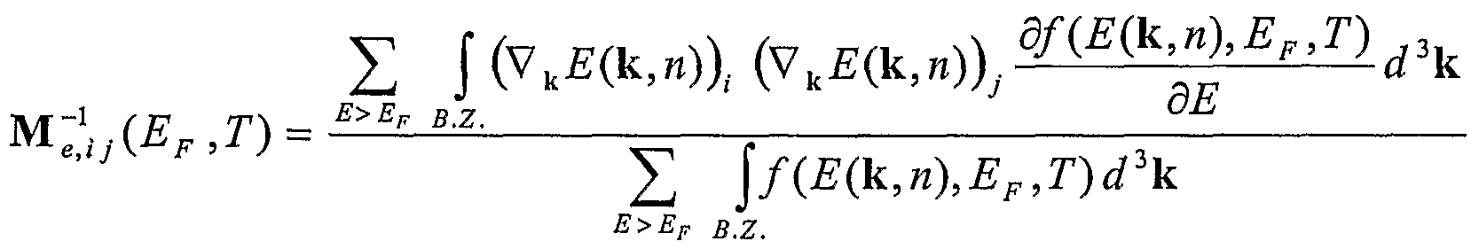
- the present invention relates to controlling the properties of semiconductor materials at the atomic or molecular level to achieve improved performance within semiconductor devices. Further, the invention relates to the identification, creation, and use of improved materials for use in the conduction paths of semiconductor devices. [0032] Applicants theorize, without wishing to be bound thereto, that certain superlattices as described herein reduce the effective mass of charge carriers and that this thereby leads to higher charge carrier mobility. Effective mass is described with various definitions in the literature. As a measure of the improvement in effective mass Applicants use a
- r " is the Fermi-Dirac distribution
- ⁇ F is the Fermi energy
- T is the temperature
- E(k,n) is the energy of an electron in the state corresponding to wave vector k and the n th energy band
- the indices i and j refer to Cartesian coordinates x, y and z
- the integrals are taken over the Brillouin zone (B. Z.)
- the summations are taken over bands with energies above and below the Fermi energy for electrons and holes respectively.
- Applicants' definition of the conductivity reciprocal effective mass tensor is such that a tensorial component of the conductivity of the material is greater for greater values of the corresponding component of the conductivity reciprocal effective mass tensor.
- the superlattices described herein set the values of the conductivity reciprocal effective mass tensor so as to enhance the conductive properties of the material, such as typically for a preferred direction of charge carrier transport .
- the inverse of the appropriate tensor element is referred to as the conductivity effective mass.
- the conductivity effective mass for electrons/holes as described above and calculated in the direction of intended carrier transport is used to distinguish improved materials.
- a strained superlattice 25 material for a channel region in a MOSFET device A planar MOSFET 20 including the strained superlattice 25 in accordance with the invention is now first described with reference to FIG. 1.
- the materials identified herein could be used in many different types of semiconductor devices, such as discrete devices and/or integrated circuits.
- another application in which the strained superlattice 25 may be used is in FINFETs, as further described in U.S. Application Serial No. 11/426,969, which is assigned to the present Assignee and is hereby incorporated herein in its entirety by reference.
- the illustrated MOSFET 20 includes a substrate 21, a stress layer 26 on the substrate, semiconductor regions 27, 28 on the stress layer, and the strained superlattice layer 25 is on the stress layer between the semiconductor regions.
- the stress layer 26 may be a graded semiconductor layer, such as a graded silicon germanium layer.
- the semiconductor regions 26, 27 may be silicon or silicon germanium regions, for example.
- the semiconductor regions 26, 27 are illustratively implanted with a dopant to provide source and drain regions 22, 23 of the MOSFET 20, as will be appreciated by those skilled in the art.
- the lattice spacing of the superlattice layer 25 would ordinarily be smaller than that of a silicon germanium stress layer 26.
- the stress layer 26 in this example induces a tensile strain in the superlattice layer 25, which may be used to provide further mobility enhancement in N-channel FETs, for example.
- the compositions of the superlattice layer 25 and stress layer 26 may be chosen so that the superlattice would otherwise have a larger lattice spacing than the stress layer. This would advantageously induce compressive strain in the superlattice layer 25 that may advantageously provide further mobility enhancement of the superlattice in P- channel FET devices, for example.
- the stress layer is a graded semiconductor layer graded in a vertical direction
- the strained superlattice 25 is vertically stacked on the graded semiconductor layer.
- the MOSFET 20' further includes a substantially ungraded semiconductor layer 42' positioned between the graded semiconductor layer 26' and a strained superlattice layer 425' . That is, the substantially ungraded semiconductor layer 42' has a substantially consistent composition of semiconductor material (e.g., silicon germanium) throughout from top to bottom and provides a buffer between the stress layer 26' and the superlattice layer 425' . More particularly, the substantially ungraded semiconductor layer 42' may have substantially the same composition as the semiconductor material at the top of the stress layer 42'.
- Source/drain suicide layers 30, 31 and source/drain contacts 32, 33 illustratively overlie the source/drain regions 22, 23, as will be appreciated by those skilled in the art.
- a gate 35 illustratively includes a gate insulating layer 37 adjacent the channel provided by the strained superlattice layer 25, and a gate electrode layer 36 on the gate insulating layer. Sidewall spacers 40, 41 are also provided in the illustrated MOSFET 20.
- the semiconductor device such as the illustrated MOSFET 20 enjoys a higher charge carrier mobility based upon the lower conductivity effective mass than would otherwise be present.
- the superlattice 25 may further have a substantially direct energy bandgap that may be particularly advantageous for opto-electronic devices, for example, such as those set forth in the co-pending application entitled INTEGRATED CIRCUIT COMPRISING AN ACTIVE OPTICAL DEVICE HAVING AN ENERGY BAND ENGINEERED SUPERLATTICE, U.S. Patent Application Serial No. 10/936,903, which is assigned to the present Assignee and is hereby incorporated herein in its entirety by reference .
- the source/drain regions 22, 23 and gate 35 of the MOSFET 20 may be considered as regions for causing the transport of charge carriers through the strained superlattice layer 25 in a parallel direction relative to the layers of the stacked groups 45a-45n, as will be discussed further below. That is, the channel of the device is defined within the superlattice 25. Other such regions are also contemplated by the present invention.
- the superlattice 25 may advantageously act as an interface for the gate dielectric layer 37.
- the channel region may be defined in the lower portion of the superlattice 25 (although some of the channel may also be defined in the semiconductor material below the superlattice) , while the upper portion thereof insulates the channel from the dielectric layer 37.
- the channel may be defined solely in the stress layer 26, and the strained superlattice layer 25 may be included merely as an insulation/interface layer.
- the superlattice 25 as a dielectric interface layer may be particularly appropriate where relatively high-K gate dielectric materials are used.
- the superlattice 25 may advantageously provide reduced scattering and, thus, enhanced mobility with respect to prior art insulation layers (e.g., silicon oxides) typically used for high-K dielectric interfaces.
- use of the superlattice 25 as an insulator for applications with high-K dielectrics may result in smaller overall thicknesses, and thus improved device capacitance. This is because the superlattice 25 may be formed in relatively small thicknesses yet still provide desired insulating properties, as discussed further in co-pending U.S. Application Serial No.
- the materials or structures are in the form of a superlattice 25 whose structure is controlled at the atomic or molecular level and may be formed using known techniques of atomic or molecular layer deposition.
- the superlattice 25 includes a plurality of layer groups 45a- 45n arranged in stacked relation, as perhaps best understood with specific reference to the schematic cross-sectional view of FIG. 2. Moreover, an intermediate annealing process as described in co-pending U.S. Application Serial No. 11/136,834, which is assigned to the present Assignee and is hereby incorporated herein in its entirety by reference, may also be used to advantageously reduce defects and provide smother layer surfaces during fabrication.
- Each group of layers 45a-45n of the superlattice 25 illustratively includes a plurality of stacked base semiconductor monolayers 46 defining a respective base semiconductor portion 46a-46n and an energy band-modifying layer 50 thereon.
- the energy band- modifying layers 50 are indicated by stippling in FIG. 2 for clarity of explanation.
- the energy-band modifying layer 50 illustratively comprises one non-semiconductor monolayer constrained within a crystal lattice of adjacent base semiconductor portions. That is, opposing base semiconductor monolayers 46 in adjacent groups of layers 45a-45n are chemically bound together. For example, in the case of silicon monolayers 46, some of the silicon atoms in the upper or top semiconductor monolayer of the group of monolayers 46a will be covalently bonded with silicon atoms in the lower or bottom monolayer of the group 46b, as seen in FIG. 3. This allows the crystal lattice to continue through the groups of layers despite the presence of the non-semiconductor monolayer (s) (e.g., oxygen monolayer (s) ) .
- s non-semiconductor monolayer
- more than one such monolayer may be possible.
- reference herein to a non-semiconductor or semiconductor monolayer means that the material used for the monolayer would be a non-semiconductor or semiconductor if formed in bulk. That is, a single monolayer of a material, such as semiconductor, may not necessarily exhibit the same properties that it would if formed in bulk or in a relatively thick layer, as will be appreciated by those skilled in the art .
- the superlattice 25 may further have a substantially direct energy bandgap that may be particularly advantageous for opto-electronic devices, for example, as described in further detail below.
- a substantially direct energy bandgap that may be particularly advantageous for opto-electronic devices, for example, as described in further detail below.
- all of the above- described properties of the superlattice 25 need not be utilized in every application.
- the superlattice 25 may only be used for its dopant blocking/insulation properties or its enhanced mobility, or it may be used for both in other applications, as will be appreciated by those skilled in the art .
- more than one non- semiconductor monolayer may be present in the energy band modifying layer 50.
- the number of non- semiconductor monolayers in the energy band-modifying layer 50 may preferably be less than about five monolayers to thereby provide the desired energy band- modifying properties.
- the superlattice 25 also illustratively includes a cap layer 52 on an upper layer group 45n.
- the cap layer 52 may comprise a plurality of base semiconductor monolayers 46.
- the cap layer 52 may have between 2 to 100 monolayers of the base semiconductor, and, more preferably between 10 to 50 monolayers.
- Each base semiconductor portion 46a-46n may comprise a base semiconductor selected from the group consisting of Group IV semiconductors, Group III-V semiconductors, and Group II-VI semiconductors.
- Group IV semiconductors also includes Group IV-IV semiconductors as will be appreciated by those skilled in the art. More particularly, the base semiconductor may comprise at least one of silicon and germanium, for example.
- Each energy band-modifying layer 50 may comprise a non-semiconductor selected from the group consisting of oxygen, nitrogen, fluorine, and carbon- oxygen, for example.
- the non-semiconductor is also desirably thermally stable through deposition of a next layer to thereby facilitate manufacturing.
- the non-semiconductor may be another inorganic or organic element or compound that is compatible with the given semiconductor processing as will be appreciated by those skilled in the art .
- the term monolayer is meant to include a single atomic layer and also a single molecular layer.
- the energy band- modifying layer 50 provided by a single monolayer is also meant to include a monolayer wherein not all of the possible sites are occupied, as noted above.
- a 4/1 repeating structure is illustrated for silicon as the base semiconductor material, and oxygen as the energy band-modifying material. Only half of the possible sites for oxygen are occupied.
- this one half occupation would not necessarily be the case, as will be appreciated by those skilled in the art . Indeed it can be seen even in this schematic diagram, that individual atoms of oxygen in a given monolayer are not precisely aligned along a flat plane as will also be appreciated by those of skill in the art of atomic deposition.
- a preferred occupation range is from about one-eighth to one-half of the possible oxygen sites being full, although other numbers may be used in certain embodiments.
- the number of silicon monolayers should desirably be seven or less so that the energy band of the superlattice is common or relatively uniform throughout to achieve the desired advantages.
- more than seven silicon layers may be used in some embodiments.
- the 4/1 repeating structure shown in FIGS. 2 and 3, for Si/0 has been modeled to indicate an enhanced mobility for electrons and holes in the X direction.
- the calculated conductivity effective mass for electrons is 0.26 and for the 4/1 SiO superlattice in the X direction it is 0.12 resulting in a ratio of 0.46.
- the calculation for holes yields values of 0.36 for bulk silicon and 0.16 for the 4/1 Si/0 superlattice resulting in a ratio of 0.44.
- other devices may benefit from a more uniform increase in mobility in any direction parallel to the groups of layers. It may also be beneficial to have an increased mobility for both electrons or holes, or just one of these types of charge carriers as will be appreciated by those skilled in the art.
- the lower conductivity effective mass for the 4/1 Si/0 embodiment of the superlattice 25 may be less than two-thirds the conductivity effective mass than would otherwise occur, and this applies for both electrons and holes.
- the superlattice 25 may further comprise at least one type of conductivity dopant therein as will also be appreciated by those skilled in the art. It may be especially appropriate to dope at least a portion of the superlattice 25 if the superlattice is to provide some or all of the channel .
- the superlattice 25 or portions thereof may also remain substantially undoped in some embodiments, as described further in U.S. Application Serial No. 11/136,757, which is assigned to the present Assignee and is hereby incorporated herein in its entirety by reference .
- FIG. 4 another embodiment of a superlattice 25' in accordance with the invention having different properties is now described.
- a repeating pattern of 3/1/5/1 is illustrated. More particularly, the lowest base semiconductor portion 46a' has three monolayers, and the second lowest base semiconductor portion 46b' has five monolayers. This pattern repeats throughout the superlattice 25' .
- the energy band-modifying layers 50' may each include a single monolayer.
- the enhancement of charge carrier mobility is independent of orientation in the plane of the layers.
- all of the base semiconductor portions of a superlattice may be a same number of monolayers thick. In other embodiments, at least some of the base semiconductor portions may be a different number of monolayers thick. In still other embodiments, all of the base semiconductor portions may be a different number of monolayers thick.
- DFT Density Functional Theory
- FIG. 5A shows the calculated band structure from the gamma point (G) for both bulk silicon (represented by continuous lines) and for the 4/1 Si/O superlattice 25 as shown in FIGS. 1-3 (represented by- dotted lines) .
- the directions refer to the unit cell of the 4/1 Si/0 structure and not to the conventional unit cell of Si, although the (001) direction in the figure does correspond to the (001) direction of the conventional unit cell of Si, and, hence, shows the expected location of the Si conduction band minimum.
- the (100) and (010) directions in the figure correspond to the (110) and (-110) directions of the conventional Si unit cell.
- the bands of Si on the figure are folded to represent them on the appropriate reciprocal lattice directions for the 4/1 Si/O structure.
- the conduction band minimum for the 4/1 Si/O structure is located at the gamma point in contrast to bulk silicon (Si) , whereas the valence band minimum occurs at the edge of the Brillouin zone in the (001) direction which we refer to as the Z point.
- the greater curvature of the conduction band minimum for the 4/1 Si/O structure compared to the curvature of the conduction band minimum for Si owing to the band splitting due to the perturbation introduced by the additional oxygen layer.
- FIG. 5B shows the calculated band structure from the Z point for both bulk silicon (continuous lines) and for the 4/1 Si/O superlattice 25 (dotted lines) . This figure illustrates the enhanced curvature of the valence band in the (100) direction.
- FIG. 5C shows the calculated band structure from the both the gamma and Z point for both bulk silicon (continuous lines) and for the 5/1/3/1 Si/0 structure of the superlattice 25' of FIG. 4 (dotted lines) . Due to the symmetry of the 5/1/3/1 Si/0 structure, the calculated band structures in the (100) and (010) directions are equivalent. Thus the conductivity effective mass and mobility are expected to be isotropic in the plane parallel to the layers, i.e. perpendicular to the (001) stacking direction. Note that in the 5/1/3/1 Si/0 example the conduction band minimum and the valence band maximum are both at or close to the Z point.
- MOSFETs 120, 220, and 320 each including a strained superlattice layer are now described.
- the various layers and regions that are similar to those discussed above with reference to FIG. 1 are represented by increments of one hundred (e.g., the substrates 121, 221, and 321 shown in FIGS. 7- 9, respectively, are similar to the substrate 21) .
- the stress layer is provided by a plurality of spaced apart strain inducing pillars 144 arranged in side-by-side relation on the backside (i.e., bottom) of the substrate 121.
- the pillars 144 may include plasma enhanced chemical vapor deposition (PECVD) silicon nitride (SiN) , metal, or other materials which become compressed upon or after being deposited in trenches etched in the backside of the substrate 121.
- PECVD plasma enhanced chemical vapor deposition
- SiN silicon nitride
- the pillars may include a thermally formed SiN material or low pressure chemical vapor deposition (LPCVD) SiN material, for example.
- LPCVD low pressure chemical vapor deposition
- an insulating layer 143 (shown with stippling for clarity of illustration) , such as an SiO 2 layer, may also be positioned between the stress layer 125 and the strained superlattice layer to provide a semiconductor-on-insulator embodiment, as shown, although the insulating layer need not be used in all embodiments.
- Further details on forming a superlattice structure as set forth above on a semiconductor-on-insulator substrate are provided in co-pending U.S. Application Serial No. 11/381,835, which is assigned to the present Assignee and is hereby incorporated herein in its entirety by reference.
- semiconductor-on-insulator implementations may be used in other embodiments discussed herein as well.
- the regions 327, 328 define a pair of spaced apart stress regions for inducing strain in the superlattice layer 125 positioned therebetween. More particularly, one or both of the stress regions may include a material that induces a desired strain on the superlattice layer 225. Using the above-noted example, for a silicon-oxygen superlattice layer 225 one or both of the regions 327, 328 may include silicon germanium.
- the silicon germanium induced a tensile strain when positioned below the superlattice layer 25, when positioned on one or both sides of the superlattice layer 225 the silicon germanium has the opposite effect and compresses the superlattice.
- silicon germanium in the stress regions 227, 228 would be advantageous for P-channel implementations because it induces compressive strain.
- a tensile strain could advantageously be induced in the superlattice layer 225 for N-channel devices by properly selecting the composition of the superlattice and the stress regions 227, 228, as discussed above.
- the spaced apart stress regions 227, 228 need not include the same materials. That is, strain may be induced as one stress region "pushes" or "pulls" against the other which serves as an anchor .
- the pair of stress regions 227, 228 are doped to provide the source and drain regions 222, 223.
- the stress regions 227, 228 illustratively include canted surfaces or facets 245, 246 adjacent opposing portions of the strained superlattice.
- the canted surfaces 245, 246 may result from the etching process used to pattern the superlattice 225 so that the stress inducing material can be deposited adjacent thereto.
- the surfaces 245, 246 need not be canted in all embodiments. Further details on making strained channel devices with strain-inducing source and drain regions are disclosed in U.S. Patent No. 6,495,402 to Yu et al. and U.S. Patent Publication No.
- the MOSFET 320 illustratively includes a stress layer 347 above the strained superlattice layer 325.
- the stress layer may be a SiN layer deposited over the source, drain, and gate regions of the MOSFET 320 that induces a strain in the underlying semiconductor material, including the superlattice layer 325.
- a tensile or compressive nitride material may be used depending upon the type of strain desired in the superlattice layer 325.
- the superlattice layer 325 may "memorize" the strain induced from the overlying stress layer 347, and the stress layer may thereafter be removed, as will be appreciated by those skilled in the art. Further details on creating strain in semiconductor regions using overlying stress layers may be found in U.S. Patent Publication Nos . 2005/0145894 to Chau et al . and 2005/0247926 to Sun et al . , both of which are hereby incorporated herein in their entireties by reference.
- a first method aspect in accordance with the invention for making a semiconductor device, such as the MOSFET 20, is now described.
- the method includes forming a stress layer 26, and forming a strained superlattice layer 25 above the stress layer.
- Another method aspect is for making a semiconductor device, such as the MOSFET 220, which includes forming a superlattice layer 225, and forming at least one pair of spaced apart stress regions 227, 228 on opposing sides of the superlattice layer to induce a strain therein.
- Still another method aspect is for making a semiconductor device, such as the MOSFET 320, which includes forming a superlattice layer 325, and forming a stress layer 347 above the strained superlattice layer to induce a strain therein.
- the strained layer need not always be a superlattice 25. Rather, the strained layer may simply • include a plurality of base semiconductor portions 46a- 46n, and one or more non-semiconductor monolayers 50 constrained within a crystal lattice of adjacent base semiconductor portions (i.e., the adjacent base semiconductor portions are chemically bound together, as described above) .
- the base semiconductor portions 46a-46n need not include a plurality of semiconductor monolayers, i.e., each semiconductor portion could include a single layer or a plurality of monolayers, for example.
- a MOSFET 80 illustratively including a non- semiconductor monolayer 81 is schematically shown in FIG. 10 wherein the semiconductor monolayers are in the portions 82a, 82b respectively below and above the non- semiconductor monolayer.
- the gate dielectric 83 is illustratively above the channel 85, and the gate electrode 84 is above the gate dielectric.
- the region between the lower portion of the gate dielectric 83 and the upper portion of the channel 85 define an interface 86.
- the source and drain (not shown) would be positioned laterally adjacent the channel 85, as will be appreciated by those skilled in the art .
- the depth of the monolayer of non-semiconductor material 81 from the interface 86 may be selected based upon the MOSFET design, as will be appreciated by those skilled in the art. For example, a depth of about 4-100 monolayers, and more preferably a depth of about 4-30 monolayers, may be selected for a typical MOSFET 86 for an oxygen layer in a silicon channel.
- the at least one monolayer of non-semiconductor material may include one or more monolayers that are not fully populated in all of the available sites as described above.
- the non-semiconductor may be selected from the group consisting of oxygen, nitrogen, fluorine, and carbon-oxygen, for example.
- the at least one monolayer of non-semiconductor material 81 may be deposited using atomic layer deposition techniques, for example, as also described above and as will be appreciated by those skilled in the art. Other deposition and/or implantation methods may also be used to form the channel 85 to include the at least one non- semiconductor material layer 81 within the crystal lattice of adjacent semiconductor layers 82a, 82b.
- a simulated plot 90 of density at the interface versus depth of an oxygen layer in Angstroms is shown in FIG. 11.
- repeating groups of the superlattice need not be used, yet the at least one non-semiconductor monolayer 81 may still provide enhancement to mobility.
Landscapes
- Engineering & Computer Science (AREA)
- Microelectronics & Electronic Packaging (AREA)
- Power Engineering (AREA)
- Physics & Mathematics (AREA)
- Ceramic Engineering (AREA)
- Condensed Matter Physics & Semiconductors (AREA)
- General Physics & Mathematics (AREA)
- Computer Hardware Design (AREA)
- Nanotechnology (AREA)
- Chemical & Material Sciences (AREA)
- Theoretical Computer Science (AREA)
- Crystallography & Structural Chemistry (AREA)
- Mathematical Physics (AREA)
- Insulated Gate Type Field-Effect Transistor (AREA)
- Thin Film Transistor (AREA)
- Recrystallisation Techniques (AREA)
Abstract
Description

Claims
Priority Applications (4)
| Application Number | Priority Date | Filing Date | Title |
|---|---|---|---|
| CA002612118A CA2612118A1 (en) | 2005-07-15 | 2006-07-14 | Semiconductor device including a strained superlattice layer above a stress layer and associated methods |
| AU2006270323A AU2006270323A1 (en) | 2005-07-15 | 2006-07-14 | Semiconductor device including a strained superlattice layer above a stress layer and associated methods |
| JP2008521585A JP2009500870A (en) | 2005-07-15 | 2006-07-14 | Semiconductor device including strained superlattice layer on stress layer and method for manufacturing the same |
| EP06787073A EP1905090A1 (en) | 2005-07-15 | 2006-07-14 | Semiconductor device including a strained superlattice layer above a stress layer and associated methods |
Applications Claiming Priority (6)
| Application Number | Priority Date | Filing Date | Title |
|---|---|---|---|
| US69994905P | 2005-07-15 | 2005-07-15 | |
| US60/699,949 | 2005-07-15 | ||
| US11/457,256 US7612366B2 (en) | 2003-06-26 | 2006-07-13 | Semiconductor device including a strained superlattice layer above a stress layer |
| US11/457,256 | 2006-07-13 | ||
| US11/457,263 | 2006-07-13 | ||
| US11/457,263 US20070010040A1 (en) | 2003-06-26 | 2006-07-13 | Method for Making a Semiconductor Device Including a Strained Superlattice Layer Above a Stress Layer |
Publications (1)
| Publication Number | Publication Date |
|---|---|
| WO2007011627A1 true WO2007011627A1 (en) | 2007-01-25 |
Family
ID=37074163
Family Applications (1)
| Application Number | Title | Priority Date | Filing Date |
|---|---|---|---|
| PCT/US2006/027119 WO2007011627A1 (en) | 2005-07-15 | 2006-07-14 | Semiconductor device including a strained superlattice layer above a stress layer and associated methods |
Country Status (6)
| Country | Link |
|---|---|
| EP (1) | EP1905090A1 (en) |
| JP (1) | JP2009500870A (en) |
| AU (1) | AU2006270323A1 (en) |
| CA (1) | CA2612118A1 (en) |
| TW (1) | TW200709410A (en) |
| WO (1) | WO2007011627A1 (en) |
Citations (6)
| Publication number | Priority date | Publication date | Assignee | Title |
|---|---|---|---|---|
| US6600170B1 (en) * | 2001-12-17 | 2003-07-29 | Advanced Micro Devices, Inc. | CMOS with strained silicon channel NMOS and silicon germanium channel PMOS |
| WO2004010485A2 (en) * | 2002-07-15 | 2004-01-29 | Infineon Technologies Ag | Semiconductor element with stress-carrying semiconductor layer and corresponding production method |
| US20040026765A1 (en) * | 2002-06-07 | 2004-02-12 | Amberwave Systems Corporation | Semiconductor devices having strained dual channel layers |
| WO2004038778A1 (en) * | 2002-10-22 | 2004-05-06 | Amberwave Systems Corporation | Gate material for semiconductor device fabrication |
| US20040266045A1 (en) * | 2003-06-26 | 2004-12-30 | Rj Mears Llc. | Method for making semiconductor device including band-engineered superlattice |
| US20050124170A1 (en) * | 2003-12-05 | 2005-06-09 | Advanced Micro Devices, Inc. | Strained semiconductor substrate and processes therefor |
-
2006
- 2006-07-14 TW TW095125960A patent/TW200709410A/en unknown
- 2006-07-14 JP JP2008521585A patent/JP2009500870A/en active Pending
- 2006-07-14 CA CA002612118A patent/CA2612118A1/en not_active Abandoned
- 2006-07-14 AU AU2006270323A patent/AU2006270323A1/en not_active Abandoned
- 2006-07-14 EP EP06787073A patent/EP1905090A1/en not_active Withdrawn
- 2006-07-14 WO PCT/US2006/027119 patent/WO2007011627A1/en active Application Filing
Patent Citations (7)
| Publication number | Priority date | Publication date | Assignee | Title |
|---|---|---|---|---|
| US6600170B1 (en) * | 2001-12-17 | 2003-07-29 | Advanced Micro Devices, Inc. | CMOS with strained silicon channel NMOS and silicon germanium channel PMOS |
| US20040026765A1 (en) * | 2002-06-07 | 2004-02-12 | Amberwave Systems Corporation | Semiconductor devices having strained dual channel layers |
| WO2004010485A2 (en) * | 2002-07-15 | 2004-01-29 | Infineon Technologies Ag | Semiconductor element with stress-carrying semiconductor layer and corresponding production method |
| WO2004038778A1 (en) * | 2002-10-22 | 2004-05-06 | Amberwave Systems Corporation | Gate material for semiconductor device fabrication |
| US20040266045A1 (en) * | 2003-06-26 | 2004-12-30 | Rj Mears Llc. | Method for making semiconductor device including band-engineered superlattice |
| WO2005013371A2 (en) * | 2003-06-26 | 2005-02-10 | Rj Mears, Llc | Semiconductor device including band-engineered superlattice |
| US20050124170A1 (en) * | 2003-12-05 | 2005-06-09 | Advanced Micro Devices, Inc. | Strained semiconductor substrate and processes therefor |
Also Published As
| Publication number | Publication date |
|---|---|
| AU2006270323A1 (en) | 2007-01-25 |
| TW200709410A (en) | 2007-03-01 |
| EP1905090A1 (en) | 2008-04-02 |
| CA2612118A1 (en) | 2007-01-25 |
| JP2009500870A (en) | 2009-01-08 |
Similar Documents
| Publication | Publication Date | Title |
|---|---|---|
| US7612366B2 (en) | Semiconductor device including a strained superlattice layer above a stress layer | |
| US7531828B2 (en) | Semiconductor device including a strained superlattice between at least one pair of spaced apart stress regions | |
| US7598515B2 (en) | Semiconductor device including a strained superlattice and overlying stress layer and related methods | |
| US20070012910A1 (en) | Semiconductor Device Including a Channel with a Non-Semiconductor Layer Monolayer | |
| US20070020833A1 (en) | Method for Making a Semiconductor Device Including a Channel with a Non-Semiconductor Layer Monolayer | |
| EP3218937B1 (en) | Method of manufacturing a semiconductor device including a superlattice and replacement metal gate structure | |
| US7491587B2 (en) | Method for making a semiconductor device having a semiconductor-on-insulator (SOI) configuration and including a superlattice on a thin semiconductor layer | |
| US20070020860A1 (en) | Method for Making Semiconductor Device Including a Strained Superlattice and Overlying Stress Layer and Related Methods | |
| US20070015344A1 (en) | Method for Making a Semiconductor Device Including a Strained Superlattice Between at Least One Pair of Spaced Apart Stress Regions | |
| US20070010040A1 (en) | Method for Making a Semiconductor Device Including a Strained Superlattice Layer Above a Stress Layer | |
| US20070063186A1 (en) | Method for making a semiconductor device including a front side strained superlattice layer and a back side stress layer | |
| WO2015077580A1 (en) | Semiconductor devices including superlattice depletion layer stack and related methods | |
| WO2007098138A2 (en) | Semiconductor device comprising a lattice matching layer and associated methods | |
| US20070063185A1 (en) | Semiconductor device including a front side strained superlattice layer and a back side stress layer | |
| WO2008091974A1 (en) | Semiconductor device with a vertical mosfet including a superlattice and related methods | |
| EP1949421A2 (en) | Method for making a semiconductor device including band-engineered superlattice using intermediate annealing | |
| US20060289049A1 (en) | Semiconductor Device Having a Semiconductor-on-Insulator (SOI) Configuration and Including a Superlattice on a Thin Semiconductor Layer | |
| US20210020749A1 (en) | Semiconductor devices including hyper-abrupt junction region including spaced-apart superlattices and related methods | |
| EP1905093A1 (en) | Semiconductor device including a channel with a non-semiconductor monolayer and associated methods | |
| EP1920466A1 (en) | Semiconductor device having a semiconductor-on-insulator (soi) configuration and including a superlattice on a thin semiconductor layer and associated methods | |
| EP1905092A1 (en) | Semiconductor device including a strained superlattice between at least one pair of spaced apart stress regions and associated methods | |
| WO2007011627A1 (en) | Semiconductor device including a strained superlattice layer above a stress layer and associated methods | |
| EP1905091A1 (en) | Semiconductor device including a strained superlattice and overlying stress layer and related methods | |
| CN114258594A (en) | Semiconductor device having a hyperabrupt junction region including a superlattice and related methods | |
| CN114270535A (en) | Varactor having a hyperabrupt junction region including a superlattice and related methods |
Legal Events
| Date | Code | Title | Description |
|---|---|---|---|
| WWE | Wipo information: entry into national phase |
Ref document number: 200680025682.5 Country of ref document: CN |
|
| 121 | Ep: the epo has been informed by wipo that ep was designated in this application | ||
| ENP | Entry into the national phase |
Ref document number: 2612118 Country of ref document: CA |
|
| WWE | Wipo information: entry into national phase |
Ref document number: 2006787073 Country of ref document: EP |
|
| ENP | Entry into the national phase |
Ref document number: 2008521585 Country of ref document: JP Kind code of ref document: A |
|
| NENP | Non-entry into the national phase |
Ref country code: DE |
|
| WWE | Wipo information: entry into national phase |
Ref document number: 2006270323 Country of ref document: AU |
|
| ENP | Entry into the national phase |
Ref document number: 2006270323 Country of ref document: AU Date of ref document: 20060714 Kind code of ref document: A |