WO2006135136A1 - Antireflective hardmask composition and methods for using same - Google Patents
Antireflective hardmask composition and methods for using same Download PDFInfo
- Publication number
- WO2006135136A1 WO2006135136A1 PCT/KR2005/003945 KR2005003945W WO2006135136A1 WO 2006135136 A1 WO2006135136 A1 WO 2006135136A1 KR 2005003945 W KR2005003945 W KR 2005003945W WO 2006135136 A1 WO2006135136 A1 WO 2006135136A1
- Authority
- WO
- WIPO (PCT)
- Prior art keywords
- composition
- group
- layer
- combination
- polymer
- Prior art date
- Legal status (The legal status is an assumption and is not a legal conclusion. Google has not performed a legal analysis and makes no representation as to the accuracy of the status listed.)
- Ceased
Links
Classifications
-
- G—PHYSICS
- G03—PHOTOGRAPHY; CINEMATOGRAPHY; ANALOGOUS TECHNIQUES USING WAVES OTHER THAN OPTICAL WAVES; ELECTROGRAPHY; HOLOGRAPHY
- G03F—PHOTOMECHANICAL PRODUCTION OF TEXTURED OR PATTERNED SURFACES, e.g. FOR PRINTING, FOR PROCESSING OF SEMICONDUCTOR DEVICES; MATERIALS THEREFOR; ORIGINALS THEREFOR; APPARATUS SPECIALLY ADAPTED THEREFOR
- G03F7/00—Photomechanical, e.g. photolithographic, production of textured or patterned surfaces, e.g. printing surfaces; Materials therefor, e.g. comprising photoresists; Apparatus specially adapted therefor
- G03F7/004—Photosensitive materials
- G03F7/09—Photosensitive materials characterised by structural details, e.g. supports, auxiliary layers
- G03F7/11—Photosensitive materials characterised by structural details, e.g. supports, auxiliary layers having cover layers or intermediate layers, e.g. subbing layers
-
- G—PHYSICS
- G03—PHOTOGRAPHY; CINEMATOGRAPHY; ANALOGOUS TECHNIQUES USING WAVES OTHER THAN OPTICAL WAVES; ELECTROGRAPHY; HOLOGRAPHY
- G03F—PHOTOMECHANICAL PRODUCTION OF TEXTURED OR PATTERNED SURFACES, e.g. FOR PRINTING, FOR PROCESSING OF SEMICONDUCTOR DEVICES; MATERIALS THEREFOR; ORIGINALS THEREFOR; APPARATUS SPECIALLY ADAPTED THEREFOR
- G03F7/00—Photomechanical, e.g. photolithographic, production of textured or patterned surfaces, e.g. printing surfaces; Materials therefor, e.g. comprising photoresists; Apparatus specially adapted therefor
- G03F7/004—Photosensitive materials
- G03F7/09—Photosensitive materials characterised by structural details, e.g. supports, auxiliary layers
- G03F7/091—Photosensitive materials characterised by structural details, e.g. supports, auxiliary layers characterised by antireflection means or light filtering or absorbing means, e.g. anti-halation, contrast enhancement
-
- G—PHYSICS
- G03—PHOTOGRAPHY; CINEMATOGRAPHY; ANALOGOUS TECHNIQUES USING WAVES OTHER THAN OPTICAL WAVES; ELECTROGRAPHY; HOLOGRAPHY
- G03F—PHOTOMECHANICAL PRODUCTION OF TEXTURED OR PATTERNED SURFACES, e.g. FOR PRINTING, FOR PROCESSING OF SEMICONDUCTOR DEVICES; MATERIALS THEREFOR; ORIGINALS THEREFOR; APPARATUS SPECIALLY ADAPTED THEREFOR
- G03F7/00—Photomechanical, e.g. photolithographic, production of textured or patterned surfaces, e.g. printing surfaces; Materials therefor, e.g. comprising photoresists; Apparatus specially adapted therefor
-
- G—PHYSICS
- G03—PHOTOGRAPHY; CINEMATOGRAPHY; ANALOGOUS TECHNIQUES USING WAVES OTHER THAN OPTICAL WAVES; ELECTROGRAPHY; HOLOGRAPHY
- G03F—PHOTOMECHANICAL PRODUCTION OF TEXTURED OR PATTERNED SURFACES, e.g. FOR PRINTING, FOR PROCESSING OF SEMICONDUCTOR DEVICES; MATERIALS THEREFOR; ORIGINALS THEREFOR; APPARATUS SPECIALLY ADAPTED THEREFOR
- G03F7/00—Photomechanical, e.g. photolithographic, production of textured or patterned surfaces, e.g. printing surfaces; Materials therefor, e.g. comprising photoresists; Apparatus specially adapted therefor
- G03F7/004—Photosensitive materials
- G03F7/038—Macromolecular compounds which are rendered insoluble or differentially wettable
- G03F7/0387—Polyamides or polyimides
-
- Y—GENERAL TAGGING OF NEW TECHNOLOGICAL DEVELOPMENTS; GENERAL TAGGING OF CROSS-SECTIONAL TECHNOLOGIES SPANNING OVER SEVERAL SECTIONS OF THE IPC; TECHNICAL SUBJECTS COVERED BY FORMER USPC CROSS-REFERENCE ART COLLECTIONS [XRACs] AND DIGESTS
- Y10—TECHNICAL SUBJECTS COVERED BY FORMER USPC
- Y10S—TECHNICAL SUBJECTS COVERED BY FORMER USPC CROSS-REFERENCE ART COLLECTIONS [XRACs] AND DIGESTS
- Y10S430/00—Radiation imagery chemistry: process, composition, or product thereof
- Y10S430/1053—Imaging affecting physical property or radiation sensitive material, or producing nonplanar or printing surface - process, composition, or product: radiation sensitive composition or product or process of making binder containing
- Y10S430/1055—Radiation sensitive composition or product or process of making
- Y10S430/114—Initiator containing
- Y10S430/115—Cationic or anionic
Definitions
- the present invention relates to hardmask compositions having antireflective properties useful in lithographic processes, and more particularly to hardmask compositions including polymers having strong absorbance in the short wavelength region (e.g., 157, 193 and 248 nm) of the electromagnetic spectrum.
- short wavelength region e.g., 157, 193 and 248 nm
- Typical lithographic processes involve pattern-wise exposure of a photosensitive resist to radiation in order to form a patterned resist layer. Thereafter, the resulting image may be developed by contacting the exposed resist layer with a suitable developing substance (e.g. an aqueous alkaline developing solution) to remove certain portions of the resist pattern. The material underlying the resist may then be etched through the openings in the resist to transfer a pattern to an underlying substrate. After the pattern is transferred, the remaining portions of the resist may then be removed.
- a suitable developing substance e.g. an aqueous alkaline developing solution
- an antireflective coating may be used to minimize the reflectivity between an imaging layer, such as a photosensitive resist, and an underlying layer.
- an imaging layer such as a photosensitive resist
- the resist does not provide sufficient etch resistance to effectively transfer the desired pattern to a layer underlying the resist. Therefore, a so-called hardmask layer may be applied as an intermediate layer between the patterned resist layer and the underlying material to be patterned. The hardmask layer receives the pattern from the patterned resist layer and should be able to withstand the etching processes needed to transfer the pattern to the underlying material.
- hardmask materials are known, there is a need for improved hardmask compositions. Since conventional hardmask materials are often difficult to apply to substrates, the use of chemical and physical vapor deposition, special solvents, and/or high-temperature baking may be required. A hardmask composition that may be applied by spin-coating techniques, and which does not require high-temperature baking, would be desirable. A hardmask composition that can be easily etched selective to the overlying photoresist, while being resistant to the etch process needed to pattern the underlying layer, would also be desirable. A hardmask composition that provides superior storage properties and avoids unwanted interactions with an imaging resist layer would further be desirable. A hardmask composition that is particularly resistant to radiation at shorter wavelengths, such as 157, 193, and 247 nm, would also be desirable.
- the present invention has been made in view of the above problems of the prior art, and it is one object of the present invention to provide novel hardmask compositions suitable for use in lithographic processes.
- antireflective hardmask compositions include:
- A is a bivalent radical selected from the group consisting of carbonyl, oxy, alkylene, fluoroalkylene, phenyldioxy, and any combination thereof;
- R and R are each independently a bivalent radical selected from the group consisting of an alkylene, an arylene, and any combination thereof; and
- x, y, and z are 0 or integers, wherein y + z > 0 and x > 0;
- the second polymer may include the following monomelic unit: [20]
- R and R may be hydrogen or methyl
- R and R may each independently be hydrogen, a crosslinking functionality, a chromophore, or any combination thereof; R may be an alkylene, a phenyldialkylene, hydroxyphenylalkylene, or any combination thereof; and n is an integer.
- methods of forming a patterned material layer on a substrate include [25] (a) forming an antireflective hardmask layer on a material layer, wherein the hardmask layer includes a composition of an embodiment of the invention;
- Fig. 1 is a flow chart illustrating a fabrication and design procedure of an integrated circuit device using a hardmask composition of the present invention.
- first, second, third etc. may be used herein to describe various elements, components, regions, layers and/or sections, these elements, components, regions, layers and/or sections should not be limited by these terms. These terms are only used to distinguish one element, component, region, layer or section from another region, layer or section. Thus, a first element, component, region, layer or section discussed below could be termed a second element, component, region, layer or section without departing from the teachings of the present invention.
- oxy refers to an -O- bivalent radical.
- alkyl and alkylene refer to a monovalent or bivalent (respectively) straight, branched, or cyclic hydrocarbon radical having from 1 to 12 carbon atoms.
- the alkyl(ene) may be a "lower alkyl(ene)" wherein the alkyl(ene) group has 1 to 4 hydrocarbons.
- lower alkyl may include methyl, ethyl, propyl, isopropyl, butyl, and iso-butyl
- lower alkylene may include methylene (-CH 2 -), ethylene (-CH 2 CH 2 -), propylene (-CH 2 CH 2 CH 2 -), isopropylene (-CH(CH 3 ) 2 -), butylene (-CH CH CH CH*-), iso-butylene (-C(CH ) CH -) and the like.
- fluoroalkylene refers to an alkylene, as defined above, wherein one or more of the hydrogen atoms is substituted with a fluoro group.
- lower fluoroalkylene refers to a "lower alkylene” group, as defined above, wherein one or more hydrogen atoms is substituted with a fluoro group.
- Exemplary lower fluoralkylene groups may include difluoromethylene and bis(trifluoromethyl)methylene,
- phenyldialkylene refers to a bivalent radical of the formula R -Ph-R -, wherein R and R are each independently alkylene groups, as defined herein, and Ph is a bivalent phenylene radical (-C H -).
- the alkylene groups may be attached at any
- phenylene 6 4 position on the phenylene ring, and the ring may be further substituted, for example, with an alkyl or a hydroxyl (-OH) group.
- exemplary phenyldialkylene groups may include benzene- 1,4-dimethyl, benzene- 1,4-diethyl, and the like.
- hydroxyphenylalkylene refers to a hydroxyphenyl-substituted alkylene, as defined herein.
- exemplary hydroxyphenylalkylene groups include hydroxyphenyl- methylene (-CH(Ph-OH)-), hydroxyphenylethylene (-CH CH(Ph-OH)-), and the like.
- the hydroxyl group may be attached at any position of the phenyl ring.
- aryl and arylene refer to a monovalent or bivalent (respectively) aromatic radical, which may optionally include 1 to 3 additional rings (e.g. cycloalkyl) fused thereto.
- the aryl(ene) rings may optionally be substituted, for example, with methyl, phenyl, or hydroxyl groups.
- Exemplary aryl(ene) groups may include:
- R and R are each independently hydrogen or methyl, and wherein R , R ,
- phenyldioxy refers to a bivalent radical of the formula 0-Ph-O-, wherein Ph is a bivalent phenylene radical (-C H -). The oxy groups may be attached at
- any position on the phenylene ring, and the ring may be further substituted, for example, with an alkyl or a hydroxyl group.
- crosslinking component refers to a compound, polymer, or the like, that may react with crosslinking functionalities of polymer(s) of the invention, in order to crosslink the polymer(s).
- the crosslinks may be formed between one type of polymer, or they may be formed between different types of polymer chains.
- Exemplary crosslinking components may include etherified amino resins, such as methylated melamine resins and butylated melamine resins (e.g. N-methoxymethyl or N- butoxymethyl melamine resins (available at Cytec Industries, Inc.)); etherified amino resins, such as methylated urea resins and butylated urea resins (e.g.
- Cymel U-65 and UFR 80 methylated/butylated glycoluril compounds (e.g. Powderlink 1174 (Cytec Industries, Inc.)); the compounds described in Canadian Patent No. 1,204,547, which is incorporated herein by reference; 2,6-bis(hydroxymethyl)-p-cresol; the compounds described in Japanese Patent Laid-Open No. 1-293339 and bis-epoxy compounds.
- methylated/butylated glycoluril compounds e.g. Powderlink 1174 (Cytec Industries, Inc.)
- the compounds described in Canadian Patent No. 1,204,547 which is incorporated herein by reference
- 2,6-bis(hydroxymethyl)-p-cresol the compounds described in Japanese Patent Laid-Open No. 1-293339 and bis-epoxy compounds.
- the term "acid catalyst” refers to any known acid catalyst,and may be, in some embodiments, a common organic acid, such as p-toluenesulfonic acid monohydrate.
- the acid catalyst may be an acid generator, whereby an acid is produced by under certain conditions.
- the acid catalyst may be a thermal acid generator (TAG) whereby an acid is generated upon thermal treatment.
- TAGs may include pyridine p-toluenesulfonic acid, 2,4,4,6-tetrabromocyclohexadienol, benzoin tosylate, 2-nitrobenzyl tosylate, and other alkyl esters of organic sulfonic acids.
- a photoacid generator may be used as the acid catalyst, whereby an acid is produced upon irradiation with a particular radiation source.
- PAGs may include those described in U.S. Patent Nos. 5,886,102 and 5,939,236, which are both incorporated herein by reference.
- crosslinking functionality refers to a functional group of a polymer of an embodiment of the invention that is capable of reacting with the crosslinking component to crosslink the polymer(s).
- exemplary crosslinking functionalities may include hydroxyl and epoxide groups.
- chromophore refers to any suitable chromophore.
- exemplary chromophores include phenyl, chrysenyl, pyrenyl, fluoranthrenyl, anthronyl, ben- zophenonyl, thioxanthonyl, anthracenyl, and anthracenyl derivatives that act as chromophores.
- exemplary anthracenyl derivatives may include 9-anthracenyl methanol.
- the chromophore contains no nitrogen, and, in other embodiments, the only nitrogen present is in the form of a deactivated amino nitrogen, such as a phenol thiazine.
- any combination thereof refers to an embodiment where two or more of the recited components are present.
- any combination thereof is used in reference to a listing of possible components, for example, acid catalysts, it is meant that two ore more of the recited acid catalysts may be used in combination.
- functional groups it is meant to include embodiments where both of the functional groups are independently present, if applicable, and also to include embodiments where the functional groups are used in combination.
- a listing of "oxy, fluoroalkylene, phenyldioxy, and any combination thereof refers to any suitable combination of the substituents, including alkylphenyldioxy (e.g. -CH CH -0-Ph-O-), fluoroalkyleneoxy (e.g. -CF CF -CH O-), and the like.
- antireflective hardmask compositions include
- A is a bivalent radical selected from the group consisting of carbonyl, oxy, alkylene, fluoroalkylene, phenyldioxy, and any combination thereof;
- R and R are each independently a bivalent radical selected from the group consisting of an alkylene, an arylene, and any combination thereof; and
- x, y, and z are 0 or integers, wherein y + z > 0 and x > 0;
- the monomeric units of the first polymer may be present in any proportion, wherein, in some embodiments, the polymer may be entirely composed of one of the two monomeric units described, while in other embodiments, the polymer may be a mixture of the two monomeric units. Further, the polymer may include other monomeric units in any proportion.
- the monomeric units may be present in any order, and their order, including in combination with other monomeric units, may be random, uniform, or in any other degree of order.
- x is an integer in a range of about 0-5, and the sum of y and z is greater than or equal to 1 and less than about 1000.
- one or more of the carboxylic acid groups of the first polymer is cyclized with the ortho-amide to form a dicarboxamide.
- [68] may, under some conditions, cyclize with the ortho-amide to form the mono- or di- carboxamide.
- the dicarboxamide is depicted below: [69]
- [72] may, under some conditions, cyclize with the ortho-amide to form the mono- or dicarboxamide.
- the dicarboxamide is depicted below: [73]
- any proportion of the polymer may contain the cyclized monomer units.
- none of the carboxylic acid groups may be cyclized with the ortho- amide, while in other embodiments, some of the carboxylic acid groups may be cyclized with the ortho-amide, and in other embodiments, many or all of the carboxylic acid groups may be cyclized with the ortho-amide.
- R and/or R may be a bivalent radical having the formula: [77]
- R and R may be hydrogen or methyl.
- R and R each may independently be alkylene, arylene, or any combination thereof, and in some embodiments, the alkylene and arylene groups comprise from 1 to 20 carbon atoms.
- the hardmask layer may not be formed to a desired thickness, and etching of the underlying layer may not be effectively acheived. However, when the polymer mixture is present in an amount exceeding about 20% by weight, etching of the hardmask layer using an upper photoresist may not be effectively conducted.
- the crosslinking component is present in an amount less than about 0.1% by weight, the hardmask layer may be damaged by an upperphotoresist solution. However, if the crosslinking component is present in an amount greater than about 5% by weight, the hardmask layer may show undesirable footing in the profile of the photoresist and/or etching of the underlying layer may be not be effectively conducted.
- the hardmask layer may be damaged by an upper photoresist solution.
- that acid catalyst is present in an amount of more than about 0.03% by weight, undesirable undercut of the profile may occur.
- the hardmask composition includes about 1 to about
- the remaining weight percent of the composition includes a solvent, in some embodiments an organic solvent, and/or a surfactant.
- the hardmask composition includes about 3-10% by weight of the polymer mixture, about 0.1-3% by weight of the crosslinking component, and about 0.001-0.03% by weight of the acid catalyst.
- the remaining weight percent of the composition includes a solvent, in some embodiments an organic solvent, and/or a surfactant.
- Exemplary solvents may include propylene glycol, monomethyl ether acetate, and other solvents commonly used with resists.
- the crosslinking component may be a melamine resin, an amino resin, a glycoluril compound, a bis-epoxy compound, or any combination thereof.
- the acid catalyst may catalyze the crosslinking of the crosslinking component with the crosslinking functionality of a polymer of an embodiment of the invention.
- the acid catalyst may be p-toluenesulfonic acid monohydrate, pyrididium p-toluenesulfonate, 2,4,4,6-tetrabromocyclohexadienone, an alkyl ester of an organic sulfonic acid, or any combination thereof.
- the alkyl ester of an organic sulfonic acid may be benzoin tosylate, 2-nitrobenzyl tosylate, or any combination thereof.
- the second polymer includes the following monomeric unit: [87]
- R and R may be hydrogen or methyl
- R and R may each independently be hydrogen, a crosslinking functionality, a
- R may be an alkylene, a phenyldialkylene, hydroxyphenylalkylene, or any combination thereof; and n is an integer.
- n is in a range of about 1 to about 190.
- the first and second polymer in some embodiments, are mixed at a ratio of about 1:99 to about 99:1. The mixing ratio may be varied according to the characteristics of the polymer composition.
- R may be methylene, benzene- 1,4-dimethyl, and hydrox- yphenylmethylene.
- the chromophore moiety is a functional group that may include phenyl, chrysenyl, pyrenyl, fluoranthrenyl, anthronyl, benzophenonyl, thioxanthonyl, anthracenyl, anthracenyl derivatives, or any combination thereof.
- the second polymer has a weight average molecular weight in a range of about 500 to about 30,000 grams per mol.
- methods of forming a patterned material layer on a substrate include [97] (a) forming an antireflective hardmask layer on a material layer, wherein the hardmask layer includes a composition of an embodiment of the invention; [98] (b) forming a radiation-sensitive imaging layer on the antireflective layer;
- the method can be carried out in accordance with the following procedure.
- a material to be patterned e.g., an aluminum or silicon nitride
- a hardmask composition according to an embodiment of the present invention may then be spin-coated onto the material.
- the composition is spin- coated to a thickness in a range of about 500 to about 4000 A.
- the hardmask composition may then be baked, for example, at a temperature in the range of about 100 to about 300 0 C, for a time in a range of about 10 seconds to about 10 minutes, to form a hardmask layer.
- a radiation-sensitive imaging layer may then be formed on the hardmask layer.
- the imaging layer may then be developed by exposing portions of the resist to radiation in order to form a pattern on the imaging layer.
- the imaging layer and the antireflective hardmask layer may then be selectively removed to expose portions of the material layer. Etching may then be performed. In some embodiments, dry etching is performed using a gas, for example, a CHF /CF mixture. After the formation of a patterned material layer, the remaining portions of the resist may be removed using a common photoresist stripper.
- hardmask compositions of the present invention and the resulting lithographic structures may be used in the fabrication and design of integrated circuit devices in semiconductor manufacture.
- the compositions and methods of embodiments of the present invention may be used, for example, in the formation of patterned material structures, such as metal wirings, holes for contacts and biases, insulating sections (e.g. damascene trenches and shallow trench isolation), and trenches for capacitor structures.
- patterned material structures such as metal wirings, holes for contacts and biases, insulating sections (e.g. damascene trenches and shallow trench isolation), and trenches for capacitor structures.
- MAK methyl amine ketone
- sample solution [117] 0.7Og of Compound 1, O.lOg of Compound 2, 0.2g of a crosslinking agent (Powderlink 1174), and 2 mg of pyridinium p-toluenesulfonate were dissolved in 9g of PGMEA, and filtered to prepare a sample solution.
- a crosslinking agent Powderlink 1174
- sample solution [126] 0.7Og of Compound 1, O.lOg of Compound 3, 0.2g of a crosslinking agent (Powderlink 1174), and 2mg of pyridinium p-toluenesulfonate were dissolved in 9g of PGMEA, and filtered to prepare a sample solution.
- a crosslinking agent Powderlink 1174
- Each of the sample solutions prepared in Examples 1 and 2 and Comparative Example 1 was spin-coated on an aluminum-coated silicon wafer and baked at 200 0 C for 60 seconds to form a 1,500 A thick film.
- a photoresist for KrF was coated on the film, baked at 110°C for 60 seconds, light-exposed using an exposure system manufactured by ASML (XT: 1400, NA 0.93), and developed with tetramethylammonium hydroxide (TMAH) (2.38 wt% aqueous solution).
- TMAH tetramethylammonium hydroxide
- a 90-nm line and space pattern was observed using an FE-SEM, and the obtained results are shown in Table 2 below.
- Exposure latitude (EL) margin according to the changes in exposure energy and depth of focus (DoF) margin according to the changes in the distance from a light source were measured, and recorded.
- compositions of the present invention may provide hardmask layers having excellent optical properties, superior mechanical properties, and high etch selectivity.
- the compositions may be easily applied by spin-coating techniques.
- the compositions may possess superior storage life and contain few or no acid pollutants.
Landscapes
- Physics & Mathematics (AREA)
- General Physics & Mathematics (AREA)
- Engineering & Computer Science (AREA)
- Architecture (AREA)
- Structural Engineering (AREA)
- Spectroscopy & Molecular Physics (AREA)
- Materials For Photolithography (AREA)
- Exposure Of Semiconductors, Excluding Electron Or Ion Beam Exposure (AREA)
- Compositions Of Macromolecular Compounds (AREA)
- Macromolecular Compounds Obtained By Forming Nitrogen-Containing Linkages In General (AREA)
Abstract
Hardmask compositions having antireflective properties useful in lithographic processes, methods of using the same, and semiconductor devices fabricated by such methods, are provided. Antireflective hardmask compositions of the invention include: (a) a polymer mixture including a first polymer that includes one or more of the following monomeric units described in this specification and a second polymer including an aryl group; (b) a crosslinking component; and (c) an acid catalyst.
Description
Description
ANTIREFLECTIVE HARDMASK COMPOSITION AND METHODS FOR USING SAME
Technical Field
[1] The present invention relates to hardmask compositions having antireflective properties useful in lithographic processes, and more particularly to hardmask compositions including polymers having strong absorbance in the short wavelength region (e.g., 157, 193 and 248 nm) of the electromagnetic spectrum.
[2]
Background Art
[3] Due to the continuous demand for smaller microelectronic devices, there exists a need to reduce the size of structural shapes in microelectronics and other related industries. Toward this end, effective lithographic techniques are essential to achieve a reduction in the size of microelectronic structures.
[4] Typical lithographic processes involve pattern-wise exposure of a photosensitive resist to radiation in order to form a patterned resist layer. Thereafter, the resulting image may be developed by contacting the exposed resist layer with a suitable developing substance (e.g. an aqueous alkaline developing solution) to remove certain portions of the resist pattern. The material underlying the resist may then be etched through the openings in the resist to transfer a pattern to an underlying substrate. After the pattern is transferred, the remaining portions of the resist may then be removed.
[5] For better resolution in lithography, an antireflective coating (ARC) may be used to minimize the reflectivity between an imaging layer, such as a photosensitive resist, and an underlying layer. However, in some lithographic imaging processes, the resist does not provide sufficient etch resistance to effectively transfer the desired pattern to a layer underlying the resist. Therefore, a so-called hardmask layer may be applied as an intermediate layer between the patterned resist layer and the underlying material to be patterned. The hardmask layer receives the pattern from the patterned resist layer and should be able to withstand the etching processes needed to transfer the pattern to the underlying material.
[6] Although a number of hardmask materials are known, there is a need for improved hardmask compositions. Since conventional hardmask materials are often difficult to apply to substrates, the use of chemical and physical vapor deposition, special solvents, and/or high-temperature baking may be required. A hardmask composition that may be applied by spin-coating techniques, and which does not require high-temperature baking, would be desirable. A hardmask composition that can be easily etched
selective to the overlying photoresist, while being resistant to the etch process needed to pattern the underlying layer, would also be desirable. A hardmask composition that provides superior storage properties and avoids unwanted interactions with an imaging resist layer would further be desirable. A hardmask composition that is particularly resistant to radiation at shorter wavelengths, such as 157, 193, and 247 nm, would also be desirable.
[7]
Disclosure of Invention Technical Problem
[8] Therefore, the present invention has been made in view of the above problems of the prior art, and it is one object of the present invention to provide novel hardmask compositions suitable for use in lithographic processes.
[9] It is another object of the present invention to provide methods for forming a patterned material layer on a substrate using the hardmask composition. [10]
Technical Solution
[H] In some embodiments of the present invention, antireflective hardmask compositions include:
[12] (a) a polymer mixture including [13] a first polymer that includes one or more of the following monomeric units [14]

[15] wherein A is a bivalent radical selected from the group consisting of carbonyl, oxy, alkylene, fluoroalkylene, phenyldioxy, and any combination thereof; R and R are each independently a bivalent radical selected from the group consisting of an alkylene, an arylene, and any combination thereof; and x, y, and z are 0 or integers, wherein y + z > 0 and x > 0; and
[16] a second polymer including an aryl group; [17] (b) a crosslinking component; and [18] (c) an acid catalyst.
[19] In some embodiments of the present invention, the second polymer may include the following monomelic unit: [20]

[21] wherein [22] R and R may be hydrogen or methyl;
5 6 [23] R and R may each independently be hydrogen, a crosslinking functionality, a chromophore, or any combination thereof; R may be an alkylene, a phenyldialkylene, hydroxyphenylalkylene, or any combination thereof; and n is an integer.
[24] In some embodiments of the present invention, methods of forming a patterned material layer on a substrate include [25] (a) forming an antireflective hardmask layer on a material layer, wherein the hardmask layer includes a composition of an embodiment of the invention;
[26] (b) forming a radiation-sensitive imaging layer on the antireflective layer; [27] (c) exposing the imaging layer to radiation; [28] (d) developing the imaging layer and the antireflective layer to expose portions of the material layer; and
[29] (e) etching the exposed portions of the material layer. [30] In some embodiments of the invention, a semiconductor integrated circuit fabricated according to a method of the invention is provided.
[31]
Brief Description of the Drawings [32] The above and other objects, features and other advantages of the present invention will be more clearly understood from the following detailed description taken in conjunction with the accompanying drawing, in which:
[33] Fig. 1 is a flow chart illustrating a fabrication and design procedure of an integrated circuit device using a hardmask composition of the present invention. [34]
Best Mode for Carrying Out the Invention
[35] The invention is described more fully hereinafter. This invention may, however, be embodied in many different forms and should not be construed as limited to the embodiments set forth herein. Rather, these embodiments are provided so that this
disclosure will be thorough and complete, and will fully convey the scope of the invention to those skilled in the art.
[36] It will be understood that when an element or layer is referred to as being "on," another element or layer, it can be directly on, connected to, or coupled to the other element or layer, or intervening elements or layers may be present. In contrast, when an element is referred to as being "directly on," "directly connected to," or "directly coupled to" another element or layer, there are no intervening elements or layers present. Like numbers refer to like elements throughout. As used herein, the term "and/ or" includes any and all combinations of one or more of the associated listed items.
[37] It will be understood that, although the terms first, second, third etc. may be used herein to describe various elements, components, regions, layers and/or sections, these elements, components, regions, layers and/or sections should not be limited by these terms. These terms are only used to distinguish one element, component, region, layer or section from another region, layer or section. Thus, a first element, component, region, layer or section discussed below could be termed a second element, component, region, layer or section without departing from the teachings of the present invention.
[38] The terminology used herein is for the purpose of describing particular embodiments only and is not intended to be limiting of the invention. As used herein, the singular forms "a", "an," and "the" are intended to include the plural forms as well, unless the context clearly indicates otherwise. It will be further understood that the terms "comprises" and/or "comprising," when used in this specification, specify the presence of stated features, integers, steps, operations, elements, and/or components, but do not preclude the presence or addition of one or more other features, integers, steps, operations, elements, components, and/or groups thereof.
[39] Unless otherwise defined, all terms (including technical and scientific terms) used herein have the same meaning as commonly understood by one of ordinary skill in the art to which this invention belongs. It will be furtherunderstood that terms, such as those defined in commonly used dictionaries, should be interpreted as having a meaning that is consistent with their meaning in the context of the relevant art and will not be interpreted in an idealized or overly formal sense unless expressly so defined herein.
[40] As used herein:
[41] The term "carbonyl" refers to a -C(=O)- bivalent radical.
[42] The term "oxy" refers to an -O- bivalent radical.
[43] The terms "alkyl" and "alkylene" refer to a monovalent or bivalent (respectively) straight, branched, or cyclic hydrocarbon radical having from 1 to 12 carbon atoms. In some embodiments, the alkyl(ene) may be a "lower alkyl(ene)" wherein the alkyl(ene)
group has 1 to 4 hydrocarbons. For example, lower alkyl may include methyl, ethyl, propyl, isopropyl, butyl, and iso-butyl, while lower alkylene may include methylene (-CH2-), ethylene (-CH2CH2-), propylene (-CH2CH2CH2-), isopropylene (-CH(CH3)2-), butylene (-CH CH CH CH*-), iso-butylene (-C(CH ) CH -) and the like.
[44] The term "fluoroalkylene" refers to an alkylene, as defined above, wherein one or more of the hydrogen atoms is substituted with a fluoro group. The term "lower fluoroalkylene" refers to a "lower alkylene" group, as defined above, wherein one or more hydrogen atoms is substituted with a fluoro group. Exemplary lower fluoralkylene groups may include difluoromethylene and bis(trifluoromethyl)methylene,
[45] The term "phenyldialkylene" refers to a bivalent radical of the formula R -Ph-R -, wherein R and R are each independently alkylene groups, as defined herein, and Ph is a bivalent phenylene radical (-C H -). The alkylene groups may be attached at any
6 4 position on the phenylene ring, and the ring may be further substituted, for example, with an alkyl or a hydroxyl (-OH) group. Exemplary phenyldialkylene groups may include benzene- 1,4-dimethyl, benzene- 1,4-diethyl, and the like.
[46] The term "hydroxyphenylalkylene" refers to a hydroxyphenyl-substituted alkylene, as defined herein. Exemplary hydroxyphenylalkylene groups include hydroxyphenyl- methylene (-CH(Ph-OH)-), hydroxyphenylethylene (-CH CH(Ph-OH)-), and the like. The hydroxyl group may be attached at any position of the phenyl ring.
[47] The terms "aryl" and "arylene" refer to a monovalent or bivalent (respectively) aromatic radical, which may optionally include 1 to 3 additional rings (e.g. cycloalkyl) fused thereto. The aryl(ene) rings may optionally be substituted, for example, with methyl, phenyl, or hydroxyl groups. Exemplary aryl(ene) groups may include:
[48]

[49] wherein R and R are each independently hydrogen or methyl, and wherein R , R ,
3 4 3 4 and the phenylene linkages may be at any position on the phenyl rings. [50] The term "phenyldioxy" refers to a bivalent radical of the formula 0-Ph-O-, wherein Ph is a bivalent phenylene radical (-C H -). The oxy groups may be attached at
6 4 any position on the phenylene ring, and the ring may be further substituted, for example, with an alkyl or a hydroxyl group.
[51] The term "crosslinking component" refers to a compound, polymer, or the like, that may react with crosslinking functionalities of polymer(s) of the invention, in order to
crosslink the polymer(s). The crosslinks may be formed between one type of polymer, or they may be formed between different types of polymer chains. Exemplary crosslinking components may include etherified amino resins, such as methylated melamine resins and butylated melamine resins (e.g. N-methoxymethyl or N- butoxymethyl melamine resins (available at Cytec Industries, Inc.)); etherified amino resins, such as methylated urea resins and butylated urea resins (e.g. Cymel U-65 and UFR 80); methylated/butylated glycoluril compounds (e.g. Powderlink 1174 (Cytec Industries, Inc.)); the compounds described in Canadian Patent No. 1,204,547, which is incorporated herein by reference; 2,6-bis(hydroxymethyl)-p-cresol; the compounds described in Japanese Patent Laid-Open No. 1-293339 and bis-epoxy compounds.
[52] The term "acid catalyst" refers to any known acid catalyst,and may be, in some embodiments, a common organic acid, such as p-toluenesulfonic acid monohydrate. In addition, in some embodiments, the acid catalyst may be an acid generator, whereby an acid is produced by under certain conditions. For example, the acid catalyst may be a thermal acid generator (TAG) whereby an acid is generated upon thermal treatment. Exemplary TAGs may include pyridine p-toluenesulfonic acid, 2,4,4,6-tetrabromocyclohexadienol, benzoin tosylate, 2-nitrobenzyl tosylate, and other alkyl esters of organic sulfonic acids. In some embodiments, a photoacid generator (PAG) may be used as the acid catalyst, whereby an acid is produced upon irradiation with a particular radiation source. Exemplary PAGs may include those described in U.S. Patent Nos. 5,886,102 and 5,939,236, which are both incorporated herein by reference.
[53] The term "crosslinking functionality" refers to a functional group of a polymer of an embodiment of the invention that is capable of reacting with the crosslinking component to crosslink the polymer(s). Exemplary crosslinking functionalities may include hydroxyl and epoxide groups.
[54] The term "chromophore" refers to any suitable chromophore. Exemplary chromophores include phenyl, chrysenyl, pyrenyl, fluoranthrenyl, anthronyl, ben- zophenonyl, thioxanthonyl, anthracenyl, and anthracenyl derivatives that act as chromophores. Exemplary anthracenyl derivatives may include 9-anthracenyl methanol. In some embodiments, the chromophore contains no nitrogen, and, in other embodiments, the only nitrogen present is in the form of a deactivated amino nitrogen, such as a phenol thiazine.
[55] The phrase "any combination thereof refers to an embodiment where two or more of the recited components are present. When the term "any combination thereof is used in reference to a listing of possible components, for example, acid catalysts, it is meant that two ore more of the recited acid catalysts may be used in combination. Further, when the phrase is used in describing a listing of functional groups, it is meant
to include embodiments where both of the functional groups are independently present, if applicable, and also to include embodiments where the functional groups are used in combination. For example, a listing of "oxy, fluoroalkylene, phenyldioxy, and any combination thereof refers to any suitable combination of the substituents, including alkylphenyldioxy (e.g. -CH CH -0-Ph-O-), fluoroalkyleneoxy (e.g. -CF CF -CH O-), and the like.
[56] In some embodiments of the present invention, antireflective hardmask compositions include
[57] (a) a polymer mixture including
[58] a first polymer that includes one or more of the following monomeric units
[59]

[60] wherein A is a bivalent radical selected from the group consisting of carbonyl, oxy, alkylene, fluoroalkylene, phenyldioxy, and any combination thereof; R and R are each independently a bivalent radical selected from the group consisting of an alkylene, an arylene, and any combination thereof; and x, y, and z are 0 or integers, wherein y + z > 0 and x > 0; and
[61] a second polymer including an aryl group;
[62] (b) a crosslinking component; and
[63] (c) an acid catalyst.
[64] The monomeric units of the first polymer may be present in any proportion, wherein, in some embodiments, the polymer may be entirely composed of one of the two monomeric units described, while in other embodiments, the polymer may be a mixture of the two monomeric units. Further, the polymer may include other monomeric units in any proportion. The monomeric units may be present in any order, and their order, including in combination with other monomeric units, may be random, uniform, or in any other degree of order.
[65] In some embodiments, x is an integer in a range of about 0-5, and the sum of y and z is greater than or equal to 1 and less than about 1000.
[66] In some embodiments, one or more of the carboxylic acid groups of the first polymer is cyclized with the ortho-amide to form a dicarboxamide. For example, the carboxylic acid groups of the monomeric unit
[67]

[68] may, under some conditions, cyclize with the ortho-amide to form the mono- or di- carboxamide. For illustration, the dicarboxamide is depicted below: [69]

[70] As another example, the carboxylic acid groups of the monomelic unit [71]

[72] may, under some conditions, cyclize with the ortho-amide to form the mono- or dicarboxamide. For illustration, the dicarboxamide is depicted below: [73]

[74] Any proportion of the polymer may contain the cyclized monomer units. In some embodiments, none of the carboxylic acid groups may be cyclized with the ortho- amide, while in other embodiments, some of the carboxylic acid groups may be cyclized with the ortho-amide, and in other embodiments, many or all of the carboxylic acid groups may be cyclized with the ortho-amide.
[75] In some embodiments, A may be carbonyl, oxy, methylene, bis(trifluoromethyl)methylene, or phenyldioxy, and x = 0 or 1.
[76] In some embodiments, R and/or R may be a bivalent radical having the formula: [77]

[78] wherein R and R may be hydrogen or methyl.
[79] In some embodiments, R and R each may independently be alkylene, arylene, or any combination thereof, and in some embodiments, the alkylene and arylene groups comprise from 1 to 20 carbon atoms.
[80] If the polymer mixture is present in an amount less than about 1 % by weight, the hardmask layer may not be formed to a desired thickness, and etching of the underlying layer may not be effectively acheived. However, when the polymer mixture is present in an amount exceeding about 20% by weight, etching of the hardmask layer using an upper photoresist may not be effectively conducted. When the crosslinking component is present in an amount less than about 0.1% by weight, the hardmask layer may be damaged by an upperphotoresist solution. However, if the crosslinking component is present in an amount greater than about 5% by weight, the hardmask layer may show undesirable footing in the profile of the photoresist and/or etching of the underlying layer may be not be effectively conducted. When the acid catalyst is present in an amount less than about 0.001% by weight, the hardmask layer may be damaged by an upper photoresist solution. However, if that acid catalyst is present in an amount of more than about 0.03% by weight, undesirable undercut of the profile may occur.
[81] Thus, in some embodiments, the hardmask composition includes about 1 to about
20% by weight of the polymer mixture; about 0.1 to about 5% by weight of the crosslinking component; and about 0.001 to about 0.05% by weight of the acid catalyst. The remaining weight percent of the composition includes a solvent, in some embodiments an organic solvent, and/or a surfactant.
[82] In some embodiments, the hardmask composition includes about 3-10% by weight of the polymer mixture, about 0.1-3% by weight of the crosslinking component, and about 0.001-0.03% by weight of the acid catalyst. The remaining weight percent of the composition includes a solvent, in some embodiments an organic solvent, and/or a surfactant.
[83] Exemplary solvents may include propylene glycol, monomethyl ether acetate, and other solvents commonly used with resists.
[84] In some embodiments, the crosslinking component may be a melamine resin, an amino resin, a glycoluril compound, a bis-epoxy compound, or any combination
thereof.
[85] The acid catalyst may catalyze the crosslinking of the crosslinking component with the crosslinking functionality of a polymer of an embodiment of the invention. In some embodiments, the acid catalyst may be p-toluenesulfonic acid monohydrate, pyrididium p-toluenesulfonate, 2,4,4,6-tetrabromocyclohexadienone, an alkyl ester of an organic sulfonic acid, or any combination thereof. In some embodiments, the alkyl ester of an organic sulfonic acid may be benzoin tosylate, 2-nitrobenzyl tosylate, or any combination thereof.
[86] In some embodiments of the present invention, the second polymer includes the following monomeric unit: [87]
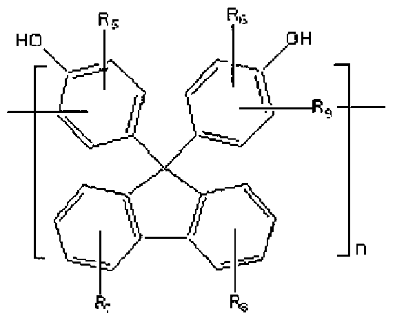
[88] wherein [89] R and R may be hydrogen or methyl;
5 6 [90] R and R may each independently be hydrogen, a crosslinking functionality, a
7 8 chromophore, or any combination thereof; R may be an alkylene, a phenyldialkylene, hydroxyphenylalkylene, or any combination thereof; and n is an integer.
[91] In some embodiments, n is in a range of about 1 to about 190. [92] The first and second polymer, in some embodiments, are mixed at a ratio of about 1:99 to about 99:1. The mixing ratio may be varied according to the characteristics of the polymer composition.
[93] In some embodiments, R may be methylene, benzene- 1,4-dimethyl, and hydrox- yphenylmethylene. [94] In some embodiments, the chromophore moiety is a functional group that may include phenyl, chrysenyl, pyrenyl, fluoranthrenyl, anthronyl, benzophenonyl, thioxanthonyl, anthracenyl, anthracenyl derivatives, or any combination thereof.
[95] In some embodiments, the second polymer has a weight average molecular weight in a range of about 500 to about 30,000 grams per mol. [96] In some embodiments of the present invention, methods of forming a patterned material layer on a substrate include [97] (a) forming an antireflective hardmask layer on a material layer, wherein the hardmask layer includes a composition of an embodiment of the invention;
[98] (b) forming a radiation-sensitive imaging layer on the antireflective layer;
[99] (c) exposing the imaging layer to radiation;
[100] (d) developing the imaging layer and the antireflective layer to expose portions of the material layer; and
[101] (e) etching the exposed portions of the material layer.
[102] In some embodiments of the invention, the method can be carried out in accordance with the following procedure. First, a material to be patterned (e.g., an aluminum or silicon nitride) may be formed onto a silicon substrate by any technique known in the art. A hardmask composition according to an embodiment of the present invention may then be spin-coated onto the material. In some embodiments, the composition is spin- coated to a thickness in a range of about 500 to about 4000 A. The hardmask composition may then be baked, for example, at a temperature in the range of about 100 to about 3000C, for a time in a range of about 10 seconds to about 10 minutes, to form a hardmask layer. A radiation-sensitive imaging layer may then be formed on the hardmask layer. The imaging layer may then be developed by exposing portions of the resist to radiation in order to form a pattern on the imaging layer. The imaging layer and the antireflective hardmask layer may then be selectively removed to expose portions of the material layer. Etching may then be performed. In some embodiments, dry etching is performed using a gas, for example, a CHF /CF mixture. After the formation of a patterned material layer, the remaining portions of the resist may be removed using a common photoresist stripper.
[103] Accordingly, hardmask compositions of the present invention and the resulting lithographic structures may be used in the fabrication and design of integrated circuit devices in semiconductor manufacture. The compositions and methods of embodiments of the present invention may be used, for example, in the formation of patterned material structures, such as metal wirings, holes for contacts and biases, insulating sections (e.g. damascene trenches and shallow trench isolation), and trenches for capacitor structures. Thus, in some embodiments of the invention, a semiconductor integrated circuit fabricated according to a method of the invention is provided.
[104]
Mode for the Invention
[105] The present invention will now be described in more detail with reference to the following examples. However, these examples are given for the purpose of illustration and are not to be construed as limiting the scope of the invention.
[106]
[107] Example 1
[108] Synthesis of Compound 1 [109]

[HO] A solution of 28.03g (0.08 moles) of 4,4'-(9-fluorenylidene)diphenol and 0.3g of p- toluenesulfonic acid in 20Og of γ-butyrolactone was charged into a one-liter four-neck flask equipped with a mechanical agitator, a condenser, a 300 ml dropping funnel and a nitrogen feed tube. The flask was heated in an stirred oil bath while it was purged with nitrogen. When the internal temperature of the reaction solution reached 1000C, 5.27 g (0.065 moles) of a 37 wt% aqueous formaldehyde solution was slowly added dropwise to the flask for 30 minutes using the dropping funnel. The reaction mixture was allowed to react for 12 hours. After completion of the reaction, the reaction flask was sufficiently cooled to room temperature. The concentration of the reaction solution was adjusted to 20 wt% by using methyl amine ketone (MAK). The solution was washed with water three times using a 3L separatory funnel, and concentrated using an evaporator. Thereafter, the concentrate was diluted with MAK and methanol to obtain a 15 wt% solution in MAK/methanol (4/1 (w/w)). The solution thus obtained was transferred to a 3L separatory funnel, and then n-heptane was added thereto to remove low molecular weight compounds containing the monomer, yielding the desired phenol resin (Mw = 4000, n = 10-11).
[111] [112] Synthesis of Compound 2 [113]

[114] 35.539g of hexafluoroisopropylidene bisphthalic dianhydride (6-FDA) was added to a solution 27.596g of 9,9-bis(4-aminophenyl)fluorene(BAFL) in 78g of N- methyl-2-pyrrolidone (NMP), and dissolved with stirring for 10 minutes. The solution was diluted with 487.6g of NMP. The dilution was stirred at room temperature for 12 hours, affording the desired product (Mn = 140K, Mw = 200K).
[115] [116] Preparation of sample solution
[117] 0.7Og of Compound 1, O.lOg of Compound 2, 0.2g of a crosslinking agent (Powderlink 1174), and 2 mg of pyridinium p-toluenesulfonate were dissolved in 9g of PGMEA, and filtered to prepare a sample solution.
[118] [119] Example 2 [120] Synthesis of Compound 3 [121]

[122] (m:n = 7:3) [123] After 22.21g of 6-FDA was added to a solution of 17.42g of BAFL in 354.9g of NMP, the resulting mixture was allowed to react with stirring for 12 hours. To the reaction mixture were added 11.8g of pyridine and 15.24g of acetic anhydride, followed by heating to 900C for one hour. NMP was further added to the reaction mixture. Pyridine, acetic anhydride, and NMP were removed by distillation to afford the desired product as a solution (Mn = 135K, Mw = 180K).
[124] [125] Preparation of sample solution [126] 0.7Og of Compound 1, O.lOg of Compound 3, 0.2g of a crosslinking agent (Powderlink 1174), and 2mg of pyridinium p-toluenesulfonate were dissolved in 9g of PGMEA, and filtered to prepare a sample solution.
[127] [128] Comparative Example 1 [129] 0.8Og of the polymer of Compound 1, 0.2Og of an oligomeric crosslinking agent (Powderlink 1174) consisting of the repeating unit shown below, and 2mg of pyridinium p-toluenesulfonate were dissolved in 9g of propyleneglycolmo- noethylacetate (PGMEA), and filtered to prepare a sample solution.
[130] [131]

[135] Each of the sample solutions prepared in Examples 1 and 2 and Comparative Example 1 was spin-coated on a silicon wafer and baked at 200°C for 60 seconds to form a 1,500 A thick film. The refractive index (n) and extinction coefficient (k) of the film were measured using an ellipsometer (J. A. Woollam). The results are shown in Table 1.
[136] Table 1

[137] [138] Comparison of 90-nm line and space pattern after application to aluminum-coated silicon wafer
[139] Each of the sample solutions prepared in Examples 1 and 2 and Comparative Example 1 was spin-coated on an aluminum-coated silicon wafer and baked at 2000C for 60 seconds to form a 1,500 A thick film. A photoresist for KrF was coated on the film, baked at 110°C for 60 seconds, light-exposed using an exposure system manufactured by ASML (XT: 1400, NA 0.93), and developed with tetramethylammonium hydroxide (TMAH) (2.38 wt% aqueous solution). A 90-nm line and space pattern was observed using an FE-SEM, and the obtained results are shown in Table 2 below. Exposure latitude (EL) margin according to the changes in exposure energy and depth of focus (DoF) margin according to the changes in the distance from a light source were measured, and recorded.
[140] Table 2
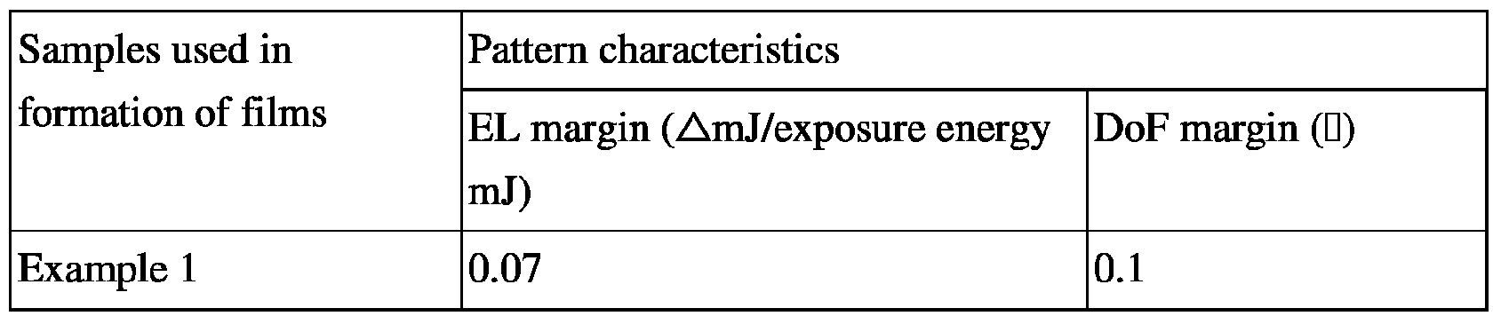

[141] [142] The patterned specimens were dry-etched using a mixed gas of CHF /CF , and
3 4 further dry-etched using a mixed gas of BCl /Cl . Finally, all remaining organic materials were removed using O , and a cross section of the specimens was observed using an FE SEM. The results are shown in Table 3.
[143] Table 3

[144] [145] The specimens were dry-etched using a mixed gas of CHF /CF , and the thickness
3 A difference before and after the dry etching was measured. The results are shown in Table 4.
[146] Table 4

[147] [148] Comparison of 80-nm line and space pattern after application to SiN-coated silicon wafer
[149] Each of the sample solutions prepared in Examples 1 and 2 and Comparative Example 1 was spin-coated onto a silicon nitride (SiN)-coated silicon wafer and baked at 2000C for 60 seconds to form a 1,500 A thick film. A photoresist for ArF was coated on the film, baked at 1100C for 60 seconds, light-exposed using an ArF exposure system (ASML1250 (FN70 5.0 active, NA 0.82), and developed with TMAH (2.38 wt% aqueous solution). An 80-nm line and space pattern was observed using an FE- SEM, and the obtained results are shown in Table 5 below. Exposure latitude (EL) margin according to the changes in exposure energy and depth of focus (DoF) margin according to the changes in the distance from a light source were measured and recorded.
[150] Table 5

[151] The patterned specimens were dry-etched using a mixed gas of CHF /CF , and
3 4 further dry-etched using a mixed gas of CHF /CF with different mixing ratios. Finally,
3 4 all remaining organic materials were removed using O , and the cross section of the specimens was observed using an FE SEM. The results are shown in Table 6.
[152] Table 6

[153]
Industrial Applicability [154] As apparent from the above description, compositions of the present invention may provide hardmask layers having excellent optical properties, superior mechanical properties, and high etch selectivity. In addition, in some embodiments, the compositions may be easily applied by spin-coating techniques. Furthermore, in some embodiments, the compositions may possess superior storage life and contain few or no acid pollutants.
[155] Although the particular embodiments of the present invention have been disclosed for illustrative purposes, those skilled in the art will appreciate that various modifications, additions and substitutions are possible, without departing from the scope and spirit of the invention as disclosed in the accompanying claims.
[156] [157]
Claims
Claims
[1] An antireflective hardmask composition, comprising:
(a) a polymer mixture comprising a first polymer comprising one or more of the following monomeric units

(b) a crosslinking component; and
(c) an acid catalyst.
[2] The composition of Claim 1, wherein x is from 0-5 and 1 < y + z < 1000. [3] The composition of Claim 1, wherein one or more of the carboxylic acid groups of the first polymer is cyclized with the ortho-amide to form a dicarboxamide.
[4] The composition of Claim 1, wherein A is a bivalent radical selected from the group consisting of carbonyl, oxy, methylene, bis(trifluoromethyl)methylene, and phenyldioxy, and x = 0 or 1.
[5] The composition of Claim 1, wherein R and/or R is a bivalent radical of the formula:

3 4
[6] The composition of Claim 1, wherein R and R are each independently a bivalent radical selected from the group consisting of alkylene, arylene, and any combination thereof, wherein said alkylene and said arylene comprise from 1 to
20 carbon atoms.
[7] The composition of Claim 1, comprising about 1 to about 20% by weight of the polymer mixture; about 0.1 to about 5% by weight of the crosslinking component; and about 0.001 to about 0.05% by weight of the acid catalyst.
[8] The composition of Claim 1, further comprising a solvent. [9] The composition of Claim 1, further comprising a surfactant. [10] The composition of Claim 1, wherein the crosslinking component is selected from the group consisting of a melamine resin, an amino resin, a glycoluril compound, a bisepoxy compound, and any combination thereof.
[H] The composition of Claim 1, wherein the acid catalyst is selected from the group consisting of p-toluenesulfonic acid monohydrate, pyrididium p- toluenesulfonate, 2,4,4,6-tetrabromocyclohexadienone, an alkyl ester of an organic sulfonic acid, and any combination thereof.
[12] The composition of Claim 11, wherein the alkyl ester of an organic sulfonic acid is selected from the group consisting of benzoin tosylate, 2-nitrobenzyl tosylate, and any combination thereof.
[13] The composition of Claim 1, wherein the second polymer comprises the monomelic unit

R and R are each independently hydrogen or methyl;
5 6
R and R are each independently selected from the group consisting of
7 o hydrogen, a crosslinking functionality, a chromophore, and any combination thereof; R is selected from the group consisting of an alkylene, a phenyl- dialkylene, hydroxyphenylalkylene, and any combination thereof; and n is an integer.
[14] The composition of Claim 13, wherein x is from 0-5, 1 < y + z < 1000, and n is from 1 to 190. [15] The composition of Claim 13, wherein one or more of the carboxylic acid groups of the first polymer is cyclized with the ortho-amide to form a dicarboxamide. [16] The composition of Claim 13, wherein A is a bivalent radical selected from the group consisting of carbonyl, oxy, methylene, bis(trifluoromethyl)methylene,
phenyldioxyl, and any combination thereof, and x = 0 or 1.
[17] TThhee ccoommjposition of Claim 13, wherein R and/or R is a bivalent radical of the formula:

3 4
[18] The composition of Claim 13, wherein R and R are each independently a bivalent radical selected from the group consisting of alkylene, arylene, and any combination thereof, wherein said alkylene and said arylene comprise from 1 to 20 carbon atoms.
[ 19] The composition of Claim 13, comprising about 1 to about 20% by weight of the polymer mixture; about 0.1 to about 5% by weight of the crosslinking component; and about 0.001 to about 0.05% by weight of the acid catalyst.
[20] The composition of Claim 13, further comprising a solvent.
[21] The composition of Claim 13, further comprising a surfactant.
[22] The composition of Claim 13, wherein the crosslinking component is selected from the group consisting of a melamine resin, an amino resin, a glycoluril compound, a bisepoxy compound, and any combination thereof.
[23] The composition of Claim 13, wherein the acid catalyst is selected from the group consisting of p-toluenesulfonic acid monohydrate, pyrididium p- toluenesulfonate, 2,4,4,6-tetrabromocyclohexadienone, an alkyl ester of an organic sulfonic acid, and any combination thereof.
[24] The composition of Claim 23, wherein the alkyl ester of an organic sulfonic acid is selected from the group consisting of benzoin tosylate, 2-nitrobenzyl tosylate, and any combination thereof.
[25] The composition of Claim 13, wherein R is a bivalent radical selected from the group consisting of methylene, benzene- 1,4-dimethyl, and hydroxyphenyl- methylene.
[26] The composition of Claim 13, wherein the chromophore moiety is a functional group selected from the group consisting of phenyl, chrysenyl, pyrenyl, fluo- ranthrenyl, anthronyl, benzophenonyl, thioxanthonyl, anthracenyl, anthracenyl derivative, and any combination thereof.
[27] The composition of Claim 13, wherein the second polymer has a weight average
molecular weight of from about 500 to about 30,000 grams per mol. [28] A method of forming a patterned material layer on a substrate, comprising
(a) forming an antireflective hardmask layer on a material layer, wherein said hardmask layer comprises the composition according to Claim 1;
(b) forming a radiation-sensitive imaging layer on the antireflective layer;
(c) exposing the imaging layer to radiation;
(d) developing the imaging layer and the antireflective layer to expose portions of the material layer; and
(e) etching the exposed portions of the material layer.
[29] A semiconductor integrated circuit fabricated using the method of Claim 28.
[30] A method of forming a patterned material layer on a substrate, comprising
(a) forming an antireflective hardmask layer on a material layer, wherein said hardmask layer comprises the composition according to Claim 13;
(b) forming a radiation-sensitive imaging layer on the antireflective layer;
(c) exposing the imaging layer to radiation;
(d) developing the imaging layer and the antireflective layer to expose portions of the material layer; and
(e) etching the exposed portions of the material layer.
[31] A semiconductor integrated circuit fabricated using the method of Claim 30.
Priority Applications (2)
| Application Number | Priority Date | Filing Date | Title |
|---|---|---|---|
| JP2008516737A JP4632379B2 (en) | 2005-06-17 | 2005-11-22 | Anti-reflective hard mask composition and method for using the same |
| CN2005800500800A CN101198907B (en) | 2005-06-17 | 2005-11-22 | Antireflective hardmask composition and methods for using same |
Applications Claiming Priority (2)
| Application Number | Priority Date | Filing Date | Title |
|---|---|---|---|
| KR1020050052169A KR100662542B1 (en) | 2005-06-17 | 2005-06-17 | Antireflective hardmask composition and method for forming patterned material shape on substrate using same |
| KR10-2005-0052169 | 2005-06-17 |
Publications (1)
| Publication Number | Publication Date |
|---|---|
| WO2006135136A1 true WO2006135136A1 (en) | 2006-12-21 |
Family
ID=37532467
Family Applications (1)
| Application Number | Title | Priority Date | Filing Date |
|---|---|---|---|
| PCT/KR2005/003945 Ceased WO2006135136A1 (en) | 2005-06-17 | 2005-11-22 | Antireflective hardmask composition and methods for using same |
Country Status (6)
| Country | Link |
|---|---|
| US (1) | US7632622B2 (en) |
| JP (1) | JP4632379B2 (en) |
| KR (1) | KR100662542B1 (en) |
| CN (1) | CN101198907B (en) |
| TW (1) | TWI295748B (en) |
| WO (1) | WO2006135136A1 (en) |
Cited By (2)
| Publication number | Priority date | Publication date | Assignee | Title |
|---|---|---|---|---|
| JP2010122297A (en) * | 2008-11-17 | 2010-06-03 | Mitsubishi Gas Chemical Co Inc | Underlayer film forming composition for lithography |
| CN104335079A (en) * | 2012-06-29 | 2015-02-04 | 国际商业机器公司 | Developable bottom antireflective coating composition and pattern forming method using thereof |
Families Citing this family (23)
| Publication number | Priority date | Publication date | Assignee | Title |
|---|---|---|---|---|
| US7829638B2 (en) * | 2005-05-09 | 2010-11-09 | Cheil Industries, Inc. | Antireflective hardmask composition and methods for using same |
| KR100655064B1 (en) * | 2005-05-27 | 2006-12-06 | 제일모직주식회사 | Hard mask composition having antireflection |
| KR100665758B1 (en) * | 2005-09-15 | 2007-01-09 | 제일모직주식회사 | Hard mask composition having antireflection |
| KR100697979B1 (en) * | 2005-09-26 | 2007-03-23 | 제일모직주식회사 | Antireflective Hardmask Composition |
| KR100782437B1 (en) * | 2005-12-30 | 2007-12-05 | 제일모직주식회사 | Liquid crystal aligning agent |
| KR100819162B1 (en) * | 2007-04-24 | 2008-04-03 | 제일모직주식회사 | Hard mask composition having anti-reflection property and patterning method of material using same |
| KR100908601B1 (en) | 2007-06-05 | 2009-07-21 | 제일모직주식회사 | Anti-reflective hard mask composition and patterning method of substrate material using same |
| KR101344794B1 (en) | 2009-12-31 | 2014-01-16 | 제일모직주식회사 | Aromatic ring-containing polymer for resist underlayer and resist underlayer composition including same |
| JP2013137334A (en) * | 2010-04-21 | 2013-07-11 | Nissan Chem Ind Ltd | Resist underlayer film-forming composition for lithography comprising resin containing polyimide structure |
| US8906590B2 (en) | 2011-03-30 | 2014-12-09 | Az Electronic Materials Usa Corp. | Antireflective coating composition and process thereof |
| JP5894106B2 (en) | 2012-06-18 | 2016-03-23 | 信越化学工業株式会社 | Compound for forming resist underlayer film, resist underlayer film material using the same, resist underlayer film forming method, pattern forming method |
| US8906592B2 (en) | 2012-08-01 | 2014-12-09 | Az Electronic Materials (Luxembourg) S.A.R.L. | Antireflective coating composition and process thereof |
| KR101599958B1 (en) * | 2012-12-26 | 2016-03-04 | 제일모직 주식회사 | Hardmask composition and method of forming patterns using the hardmask composition |
| US9152051B2 (en) | 2013-06-13 | 2015-10-06 | Az Electronics Materials (Luxembourg) S.A.R.L. | Antireflective coating composition and process thereof |
| WO2015026194A1 (en) * | 2013-08-23 | 2015-02-26 | (주)디엔에프 | Novel polymer and composition containing same |
| KR101582462B1 (en) * | 2013-08-23 | 2016-01-06 | (주)디엔에프 | new polymer and compositions containing it |
| KR101788093B1 (en) | 2014-03-19 | 2017-10-19 | 제일모직 주식회사 | Monomer for hardmask composition and hardmask composition including the monomer and method of forming patterns using the hardmask composition |
| KR101754901B1 (en) | 2014-05-16 | 2017-07-06 | 제일모직 주식회사 | Hardmask composition and method of forming patterns using the hardmask composition |
| JP6711104B2 (en) * | 2015-04-24 | 2020-06-17 | Jsr株式会社 | Resist underlayer film forming method and pattern forming method |
| KR102697981B1 (en) * | 2018-01-23 | 2024-08-23 | 제이에스알 가부시끼가이샤 | Composition for forming a resist underlayer film, resist underlayer film and method for forming the same, and method for manufacturing a patterned substrate |
| KR102513862B1 (en) * | 2018-06-01 | 2023-03-23 | 최상준 | A composition of anti-reflective hardmask |
| KR102244470B1 (en) | 2018-07-18 | 2021-04-23 | 삼성에스디아이 주식회사 | Polymer, organic layer composition and method of forming patterns |
| WO2026083948A1 (en) * | 2024-10-16 | 2026-04-23 | Jsr株式会社 | Composition for forming nitrogen-containing film and method for manufacturing semiconductor substrate |
Citations (4)
| Publication number | Priority date | Publication date | Assignee | Title |
|---|---|---|---|---|
| JP2002148791A (en) * | 2000-11-09 | 2002-05-22 | Tokyo Ohka Kogyo Co Ltd | Composition for forming antireflection film |
| US6503692B2 (en) * | 2000-06-23 | 2003-01-07 | International Business Machines Corporation | Antireflective silicon-containing compositions as hardmask layer |
| EP1378796A1 (en) * | 2001-04-10 | 2004-01-07 | Nissan Chemical Industries, Ltd. | Composition for forming antireflection film for lithography |
| JP2004341479A (en) * | 2002-12-02 | 2004-12-02 | Tokyo Ohka Kogyo Co Ltd | Composition for forming antireflection film and ladder type silicone copolymer used therefor |
Family Cites Families (30)
| Publication number | Priority date | Publication date | Assignee | Title |
|---|---|---|---|---|
| EP0058638B1 (en) | 1981-02-13 | 1985-08-28 | Ciba-Geigy Ag | Curable compositions containing an acid-curable resin, and process for curing them |
| JPS5940641A (en) * | 1982-08-31 | 1984-03-06 | Toshiba Corp | Negative type photoresist composition used for high resolution image |
| JPH01293339A (en) | 1988-05-23 | 1989-11-27 | Tosoh Corp | Photoresist composition |
| DE69128187T2 (en) * | 1990-09-28 | 1998-03-26 | Toshiba Kawasaki Kk | Photosensitive resin composition for producing a polyimide film pattern and method for producing a polyimide film pattern |
| US6165697A (en) * | 1991-11-15 | 2000-12-26 | Shipley Company, L.L.C. | Antihalation compositions |
| JP3332100B2 (en) * | 1992-03-24 | 2002-10-07 | 株式会社東芝 | Pattern formation method |
| JP3117103B2 (en) | 1992-06-23 | 2000-12-11 | 日産化学工業株式会社 | New vertical alignment agent |
| JP3212162B2 (en) | 1992-10-22 | 2001-09-25 | 日産化学工業株式会社 | Diaminobenzene derivative, polyimide and liquid crystal alignment film |
| JP3206401B2 (en) | 1995-11-20 | 2001-09-10 | ジェイエスアール株式会社 | Liquid crystal alignment agent and liquid crystal display device |
| US5886102A (en) | 1996-06-11 | 1999-03-23 | Shipley Company, L.L.C. | Antireflective coating compositions |
| US5939236A (en) | 1997-02-07 | 1999-08-17 | Shipley Company, L.L.C. | Antireflective coating compositions comprising photoacid generators |
| JPH1184391A (en) | 1997-09-04 | 1999-03-26 | Nissan Chem Ind Ltd | Liquid crystal orientation treating agent |
| US6890448B2 (en) * | 1999-06-11 | 2005-05-10 | Shipley Company, L.L.C. | Antireflective hard mask compositions |
| JP3676958B2 (en) * | 1999-12-28 | 2005-07-27 | 株式会社日立製作所 | Manufacturing method of semiconductor integrated circuit device |
| US6599675B2 (en) * | 2000-04-28 | 2003-07-29 | Mitsui Chemicals, Inc. | Polyimides and polyamic acids |
| JP4404330B2 (en) * | 2001-01-09 | 2010-01-27 | 東京応化工業株式会社 | Photopolymerizable composition and method for producing color filter using the composition |
| JP4799740B2 (en) * | 2001-01-17 | 2011-10-26 | 日東電工株式会社 | Resin composition for printed circuit board, substrate for wired circuit board, and wired circuit board |
| US6844131B2 (en) * | 2002-01-09 | 2005-01-18 | Clariant Finance (Bvi) Limited | Positive-working photoimageable bottom antireflective coating |
| US7070914B2 (en) * | 2002-01-09 | 2006-07-04 | Az Electronic Materials Usa Corp. | Process for producing an image using a first minimum bottom antireflective coating composition |
| JP4380178B2 (en) * | 2002-03-28 | 2009-12-09 | 日立化成デュポンマイクロシステムズ株式会社 | Positive photosensitive resin composition, pattern manufacturing method, and electronic component |
| JP2003295430A (en) * | 2002-03-29 | 2003-10-15 | Kyocera Chemical Corp | Photosensitive resin composition and positive pattern forming method |
| JP3994270B2 (en) * | 2002-06-25 | 2007-10-17 | 日産化学工業株式会社 | Method for forming antireflection film |
| JP4355943B2 (en) * | 2003-10-03 | 2009-11-04 | 信越化学工業株式会社 | Photoresist underlayer film forming material and pattern forming method |
| US7303855B2 (en) * | 2003-10-03 | 2007-12-04 | Shin-Etsu Chemical Co., Ltd. | Photoresist undercoat-forming material and patterning process |
| US20050255410A1 (en) * | 2004-04-29 | 2005-11-17 | Guerrero Douglas J | Anti-reflective coatings using vinyl ether crosslinkers |
| US7829638B2 (en) | 2005-05-09 | 2010-11-09 | Cheil Industries, Inc. | Antireflective hardmask composition and methods for using same |
| KR100655064B1 (en) | 2005-05-27 | 2006-12-06 | 제일모직주식회사 | Hard mask composition having antireflection |
| KR100665758B1 (en) | 2005-09-15 | 2007-01-09 | 제일모직주식회사 | Hard mask composition having antireflection |
| KR100697979B1 (en) | 2005-09-26 | 2007-03-23 | 제일모직주식회사 | Antireflective Hardmask Composition |
| KR100782437B1 (en) | 2005-12-30 | 2007-12-05 | 제일모직주식회사 | Liquid crystal aligning agent |
-
2005
- 2005-06-17 KR KR1020050052169A patent/KR100662542B1/en not_active Expired - Lifetime
- 2005-11-22 JP JP2008516737A patent/JP4632379B2/en not_active Expired - Lifetime
- 2005-11-22 WO PCT/KR2005/003945 patent/WO2006135136A1/en not_active Ceased
- 2005-11-22 CN CN2005800500800A patent/CN101198907B/en not_active Expired - Lifetime
- 2005-11-25 TW TW094141501A patent/TWI295748B/en not_active IP Right Cessation
- 2005-12-12 US US11/301,049 patent/US7632622B2/en active Active
Patent Citations (4)
| Publication number | Priority date | Publication date | Assignee | Title |
|---|---|---|---|---|
| US6503692B2 (en) * | 2000-06-23 | 2003-01-07 | International Business Machines Corporation | Antireflective silicon-containing compositions as hardmask layer |
| JP2002148791A (en) * | 2000-11-09 | 2002-05-22 | Tokyo Ohka Kogyo Co Ltd | Composition for forming antireflection film |
| EP1378796A1 (en) * | 2001-04-10 | 2004-01-07 | Nissan Chemical Industries, Ltd. | Composition for forming antireflection film for lithography |
| JP2004341479A (en) * | 2002-12-02 | 2004-12-02 | Tokyo Ohka Kogyo Co Ltd | Composition for forming antireflection film and ladder type silicone copolymer used therefor |
Cited By (3)
| Publication number | Priority date | Publication date | Assignee | Title |
|---|---|---|---|---|
| JP2010122297A (en) * | 2008-11-17 | 2010-06-03 | Mitsubishi Gas Chemical Co Inc | Underlayer film forming composition for lithography |
| CN104335079A (en) * | 2012-06-29 | 2015-02-04 | 国际商业机器公司 | Developable bottom antireflective coating composition and pattern forming method using thereof |
| CN104335079B (en) * | 2012-06-29 | 2016-01-13 | 国际商业机器公司 | Can be developed bottom antireflective coating composition and use its pattern formation method |
Also Published As
| Publication number | Publication date |
|---|---|
| US20070003863A1 (en) | 2007-01-04 |
| KR100662542B1 (en) | 2006-12-28 |
| CN101198907A (en) | 2008-06-11 |
| TWI295748B (en) | 2008-04-11 |
| JP2008547045A (en) | 2008-12-25 |
| CN101198907B (en) | 2011-08-31 |
| KR20060132069A (en) | 2006-12-21 |
| TW200700923A (en) | 2007-01-01 |
| US7632622B2 (en) | 2009-12-15 |
| JP4632379B2 (en) | 2011-02-16 |
Similar Documents
| Publication | Publication Date | Title |
|---|---|---|
| US7632622B2 (en) | Antireflective hardmask composition and methods for using same | |
| US7829638B2 (en) | Antireflective hardmask composition and methods for using same | |
| US7378217B2 (en) | Antireflective hardmask composition and methods for using same | |
| JP4681047B2 (en) | Anti-reflective hard mask composition and method of use thereof | |
| US7655386B2 (en) | Polymer having antireflective properties, hardmask composition including the same, process for forming a patterned material layer, and associated device | |
| US8153349B2 (en) | Polymer composition, hardmask composition having antireflective properties, and associated methods | |
| KR101414278B1 (en) | Polymer for under-layer of resist, polymer composition, under-layer composition of resist, of patterning device using same | |
| US8420289B2 (en) | Aromatic ring-containing polymer, polymer mixture, antireflective hardmask composition, and associated methods | |
| US7862990B2 (en) | Polymer having antireflective properties and high carbon content, hardmask composition including the same, and process for forming a patterned material layer | |
| US7981594B2 (en) | Hardmask composition having antirelective properties and method of patterning material on susbstrate using the same | |
| WO2008082236A1 (en) | Polymer having antireflective properties, hardmask composition including the same, and process for forming a patterned material layer | |
| KR101174086B1 (en) | Polymer, polymer composition, under-layer composition of resist, and patterning method of materials using the same | |
| US7405029B2 (en) | Antireflective hardmask composition and methods for using same | |
| US9170494B2 (en) | Antireflective compositions and methods of using same | |
| KR20100080147A (en) | Polymer, polymer composition, under-layer composition of resist, and patterning method of materials using the same | |
| WO2007139268A1 (en) | Antireflective hardmask composition | |
| KR100671117B1 (en) | Hard mask composition having antireflection | |
| KR100671114B1 (en) | Hard mask composition having antireflection | |
| KR20100078851A (en) | Polymer, polymer composition, under-layer composition of resist, and patterning method of materials using the same |
Legal Events
| Date | Code | Title | Description |
|---|---|---|---|
| WWE | Wipo information: entry into national phase |
Ref document number: 200580050080.0 Country of ref document: CN |
|
| 121 | Ep: the epo has been informed by wipo that ep was designated in this application | ||
| ENP | Entry into the national phase |
Ref document number: 2008516737 Country of ref document: JP Kind code of ref document: A |
|
| NENP | Non-entry into the national phase |
Ref country code: DE |
|
| 122 | Ep: pct application non-entry in european phase |
Ref document number: 05820688 Country of ref document: EP Kind code of ref document: A1 |