WO2006094645A1 - Monomers, oligomers and polymers comprising thiophene and selenophene - Google Patents
Monomers, oligomers and polymers comprising thiophene and selenophene Download PDFInfo
- Publication number
- WO2006094645A1 WO2006094645A1 PCT/EP2006/001664 EP2006001664W WO2006094645A1 WO 2006094645 A1 WO2006094645 A1 WO 2006094645A1 EP 2006001664 W EP2006001664 W EP 2006001664W WO 2006094645 A1 WO2006094645 A1 WO 2006094645A1
- Authority
- WO
- WIPO (PCT)
- Prior art keywords
- compounds
- polymerisable
- alkyl
- independently
- polymer
- Prior art date
Links
- 0 Cc1c(C)[s]c(Br)c1* Chemical compound Cc1c(C)[s]c(Br)c1* 0.000 description 2
Classifications
-
- C—CHEMISTRY; METALLURGY
- C08—ORGANIC MACROMOLECULAR COMPOUNDS; THEIR PREPARATION OR CHEMICAL WORKING-UP; COMPOSITIONS BASED THEREON
- C08G—MACROMOLECULAR COMPOUNDS OBTAINED OTHERWISE THAN BY REACTIONS ONLY INVOLVING UNSATURATED CARBON-TO-CARBON BONDS
- C08G79/00—Macromolecular compounds obtained by reactions forming a linkage containing atoms other than silicon, sulfur, nitrogen, oxygen, and carbon with or without the latter elements in the main chain of the macromolecule
-
- H—ELECTRICITY
- H01—ELECTRIC ELEMENTS
- H01B—CABLES; CONDUCTORS; INSULATORS; SELECTION OF MATERIALS FOR THEIR CONDUCTIVE, INSULATING OR DIELECTRIC PROPERTIES
- H01B1/00—Conductors or conductive bodies characterised by the conductive materials; Selection of materials as conductors
- H01B1/06—Conductors or conductive bodies characterised by the conductive materials; Selection of materials as conductors mainly consisting of other non-metallic substances
- H01B1/12—Conductors or conductive bodies characterised by the conductive materials; Selection of materials as conductors mainly consisting of other non-metallic substances organic substances
- H01B1/124—Intrinsically conductive polymers
- H01B1/127—Intrinsically conductive polymers comprising five-membered aromatic rings in the main chain, e.g. polypyrroles, polythiophenes
-
- C—CHEMISTRY; METALLURGY
- C07—ORGANIC CHEMISTRY
- C07D—HETEROCYCLIC COMPOUNDS
- C07D421/00—Heterocyclic compounds containing two or more hetero rings, at least one ring having selenium, tellurium, or halogen atoms as ring hetero atoms
- C07D421/14—Heterocyclic compounds containing two or more hetero rings, at least one ring having selenium, tellurium, or halogen atoms as ring hetero atoms containing three or more hetero rings
-
- C—CHEMISTRY; METALLURGY
- C08—ORGANIC MACROMOLECULAR COMPOUNDS; THEIR PREPARATION OR CHEMICAL WORKING-UP; COMPOSITIONS BASED THEREON
- C08G—MACROMOLECULAR COMPOUNDS OBTAINED OTHERWISE THAN BY REACTIONS ONLY INVOLVING UNSATURATED CARBON-TO-CARBON BONDS
- C08G61/00—Macromolecular compounds obtained by reactions forming a carbon-to-carbon link in the main chain of the macromolecule
- C08G61/12—Macromolecular compounds containing atoms other than carbon in the main chain of the macromolecule
- C08G61/122—Macromolecular compounds containing atoms other than carbon in the main chain of the macromolecule derived from five- or six-membered heterocyclic compounds, other than imides
- C08G61/123—Macromolecular compounds containing atoms other than carbon in the main chain of the macromolecule derived from five- or six-membered heterocyclic compounds, other than imides derived from five-membered heterocyclic compounds
- C08G61/126—Macromolecular compounds containing atoms other than carbon in the main chain of the macromolecule derived from five- or six-membered heterocyclic compounds, other than imides derived from five-membered heterocyclic compounds with a five-membered ring containing one sulfur atom in the ring
-
- C—CHEMISTRY; METALLURGY
- C08—ORGANIC MACROMOLECULAR COMPOUNDS; THEIR PREPARATION OR CHEMICAL WORKING-UP; COMPOSITIONS BASED THEREON
- C08G—MACROMOLECULAR COMPOUNDS OBTAINED OTHERWISE THAN BY REACTIONS ONLY INVOLVING UNSATURATED CARBON-TO-CARBON BONDS
- C08G75/00—Macromolecular compounds obtained by reactions forming a linkage containing sulfur with or without nitrogen, oxygen, or carbon in the main chain of the macromolecule
- C08G75/02—Polythioethers
- C08G75/06—Polythioethers from cyclic thioethers
-
- C—CHEMISTRY; METALLURGY
- C09—DYES; PAINTS; POLISHES; NATURAL RESINS; ADHESIVES; COMPOSITIONS NOT OTHERWISE PROVIDED FOR; APPLICATIONS OF MATERIALS NOT OTHERWISE PROVIDED FOR
- C09K—MATERIALS FOR MISCELLANEOUS APPLICATIONS, NOT PROVIDED FOR ELSEWHERE
- C09K11/00—Luminescent, e.g. electroluminescent, chemiluminescent materials
- C09K11/06—Luminescent, e.g. electroluminescent, chemiluminescent materials containing organic luminescent materials
-
- C—CHEMISTRY; METALLURGY
- C09—DYES; PAINTS; POLISHES; NATURAL RESINS; ADHESIVES; COMPOSITIONS NOT OTHERWISE PROVIDED FOR; APPLICATIONS OF MATERIALS NOT OTHERWISE PROVIDED FOR
- C09K—MATERIALS FOR MISCELLANEOUS APPLICATIONS, NOT PROVIDED FOR ELSEWHERE
- C09K19/00—Liquid crystal materials
- C09K19/04—Liquid crystal materials characterised by the chemical structure of the liquid crystal components, e.g. by a specific unit
- C09K19/06—Non-steroidal liquid crystal compounds
- C09K19/34—Non-steroidal liquid crystal compounds containing at least one heterocyclic ring
- C09K19/3491—Non-steroidal liquid crystal compounds containing at least one heterocyclic ring having sulfur as hetero atom
-
- C—CHEMISTRY; METALLURGY
- C09—DYES; PAINTS; POLISHES; NATURAL RESINS; ADHESIVES; COMPOSITIONS NOT OTHERWISE PROVIDED FOR; APPLICATIONS OF MATERIALS NOT OTHERWISE PROVIDED FOR
- C09K—MATERIALS FOR MISCELLANEOUS APPLICATIONS, NOT PROVIDED FOR ELSEWHERE
- C09K19/00—Liquid crystal materials
- C09K19/04—Liquid crystal materials characterised by the chemical structure of the liquid crystal components, e.g. by a specific unit
- C09K19/38—Polymers
- C09K19/3804—Polymers with mesogenic groups in the main chain
-
- C—CHEMISTRY; METALLURGY
- C09—DYES; PAINTS; POLISHES; NATURAL RESINS; ADHESIVES; COMPOSITIONS NOT OTHERWISE PROVIDED FOR; APPLICATIONS OF MATERIALS NOT OTHERWISE PROVIDED FOR
- C09K—MATERIALS FOR MISCELLANEOUS APPLICATIONS, NOT PROVIDED FOR ELSEWHERE
- C09K19/00—Liquid crystal materials
- C09K19/04—Liquid crystal materials characterised by the chemical structure of the liquid crystal components, e.g. by a specific unit
- C09K19/40—Liquid crystal materials characterised by the chemical structure of the liquid crystal components, e.g. by a specific unit containing elements other than carbon, hydrogen, halogen, oxygen, nitrogen or sulfur, e.g. silicon, metals
-
- H—ELECTRICITY
- H01—ELECTRIC ELEMENTS
- H01B—CABLES; CONDUCTORS; INSULATORS; SELECTION OF MATERIALS FOR THEIR CONDUCTIVE, INSULATING OR DIELECTRIC PROPERTIES
- H01B1/00—Conductors or conductive bodies characterised by the conductive materials; Selection of materials as conductors
- H01B1/06—Conductors or conductive bodies characterised by the conductive materials; Selection of materials as conductors mainly consisting of other non-metallic substances
- H01B1/12—Conductors or conductive bodies characterised by the conductive materials; Selection of materials as conductors mainly consisting of other non-metallic substances organic substances
-
- H—ELECTRICITY
- H05—ELECTRIC TECHNIQUES NOT OTHERWISE PROVIDED FOR
- H05B—ELECTRIC HEATING; ELECTRIC LIGHT SOURCES NOT OTHERWISE PROVIDED FOR; CIRCUIT ARRANGEMENTS FOR ELECTRIC LIGHT SOURCES, IN GENERAL
- H05B33/00—Electroluminescent light sources
- H05B33/12—Light sources with substantially two-dimensional radiating surfaces
- H05B33/14—Light sources with substantially two-dimensional radiating surfaces characterised by the chemical or physical composition or the arrangement of the electroluminescent material, or by the simultaneous addition of the electroluminescent material in or onto the light source
-
- H—ELECTRICITY
- H10—SEMICONDUCTOR DEVICES; ELECTRIC SOLID-STATE DEVICES NOT OTHERWISE PROVIDED FOR
- H10K—ORGANIC ELECTRIC SOLID-STATE DEVICES
- H10K85/00—Organic materials used in the body or electrodes of devices covered by this subclass
- H10K85/10—Organic polymers or oligomers
- H10K85/111—Organic polymers or oligomers comprising aromatic, heteroaromatic, or aryl chains, e.g. polyaniline, polyphenylene or polyphenylene vinylene
- H10K85/113—Heteroaromatic compounds comprising sulfur or selene, e.g. polythiophene
-
- C—CHEMISTRY; METALLURGY
- C09—DYES; PAINTS; POLISHES; NATURAL RESINS; ADHESIVES; COMPOSITIONS NOT OTHERWISE PROVIDED FOR; APPLICATIONS OF MATERIALS NOT OTHERWISE PROVIDED FOR
- C09K—MATERIALS FOR MISCELLANEOUS APPLICATIONS, NOT PROVIDED FOR ELSEWHERE
- C09K2211/00—Chemical nature of organic luminescent or tenebrescent compounds
- C09K2211/14—Macromolecular compounds
- C09K2211/1441—Heterocyclic
- C09K2211/1483—Heterocyclic containing nitrogen and sulfur as heteroatoms
-
- C—CHEMISTRY; METALLURGY
- C09—DYES; PAINTS; POLISHES; NATURAL RESINS; ADHESIVES; COMPOSITIONS NOT OTHERWISE PROVIDED FOR; APPLICATIONS OF MATERIALS NOT OTHERWISE PROVIDED FOR
- C09K—MATERIALS FOR MISCELLANEOUS APPLICATIONS, NOT PROVIDED FOR ELSEWHERE
- C09K2211/00—Chemical nature of organic luminescent or tenebrescent compounds
- C09K2211/14—Macromolecular compounds
- C09K2211/1441—Heterocyclic
- C09K2211/1491—Heterocyclic containing other combinations of heteroatoms
-
- C—CHEMISTRY; METALLURGY
- C09—DYES; PAINTS; POLISHES; NATURAL RESINS; ADHESIVES; COMPOSITIONS NOT OTHERWISE PROVIDED FOR; APPLICATIONS OF MATERIALS NOT OTHERWISE PROVIDED FOR
- C09K—MATERIALS FOR MISCELLANEOUS APPLICATIONS, NOT PROVIDED FOR ELSEWHERE
- C09K2323/00—Functional layers of liquid crystal optical display excluding electroactive liquid crystal layer characterised by chemical composition
-
- Y—GENERAL TAGGING OF NEW TECHNOLOGICAL DEVELOPMENTS; GENERAL TAGGING OF CROSS-SECTIONAL TECHNOLOGIES SPANNING OVER SEVERAL SECTIONS OF THE IPC; TECHNICAL SUBJECTS COVERED BY FORMER USPC CROSS-REFERENCE ART COLLECTIONS [XRACs] AND DIGESTS
- Y02—TECHNOLOGIES OR APPLICATIONS FOR MITIGATION OR ADAPTATION AGAINST CLIMATE CHANGE
- Y02E—REDUCTION OF GREENHOUSE GAS [GHG] EMISSIONS, RELATED TO ENERGY GENERATION, TRANSMISSION OR DISTRIBUTION
- Y02E10/00—Energy generation through renewable energy sources
- Y02E10/50—Photovoltaic [PV] energy
- Y02E10/549—Organic PV cells
Definitions
- the invention relates to novel mono-, oligo- and polymeric compounds comprising thiophene and selenophene.
- the invention further relates to their use as semiconductors or charge transport materials, in optical, electro-optical or electronic devices.
- the invention further relates to optical, electro-optical or electronic devices comprising the novel compounds.
- Organic materials have recently shown promise as the active layer in organic based thin film transistors and organic field effect transistors [see H. E. Katz, Z. Bao and S. L. Gilat, >Acc. Chem. Res., 2001 , 34, 5, 359]. Such devices have potential applications in smart cards, security tags and the switching element in flat panel displays. Organic materials are envisaged to have substantial cost advantages over their silicon analogues if they can be deposited from solution, as this enables a fast, large-area fabrication route.
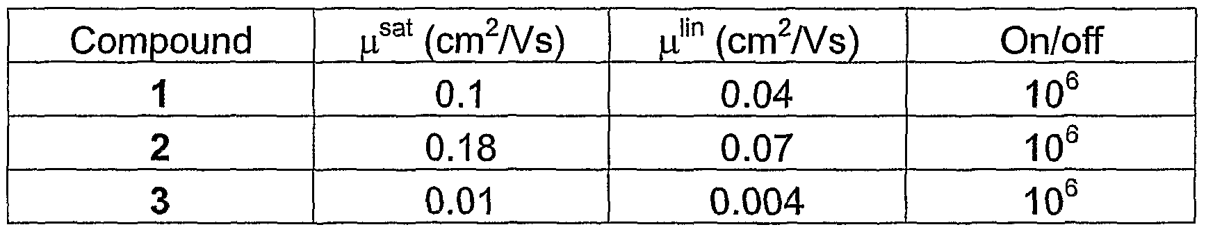
- the performance of the device is principally based upon the charge carrier mobility of the semi-conducting material and the current on/off ratio, so the ideal semiconductor should have a low conductivity in the off state, combined with a high charge carrier mobility (> 1 x 10 '3 cm 2 V "1 s '1 ).
- the semi-conducting material is relatively stable to oxidation i.e. it has a high ionization potential, as oxidation leads to reduced device performance.
- a high regioregularity leads to improved packing and optimised microstructure, leading to improved charge carrier mobility [see H. Sirringhaus et al., Science, 1998, 280, 1741-1744; H. Sirringhaus et al., Nature, 1999, 401, 685-688; and H. Sirringhaus, et al., Synthetic Metals, 2000, 111-112, 129-132].
- poly(3-alkylthiophenes) show improved solubility and are able to be solution processed to fabricate large area films.
- po!y(3-alkylthiophenes) have relatively low ionisation potentials and are susceptible to doping in air.
- EP-A-1 439 590 discloses mono-, oligo- and poly-bis(thienyl) arylenes, but does not disclose compounds of the present invention.
- S. Tierney, M. Heeney and I. McCulloch, Synth Met, 148(2), 195- 198, (2005) discloses poly-bis(3-octyl-thiophen-2-yl) selenophene, but does not disclose compounds of the present invention.
- the invention relates to monomeric, oligomeric or polymeric compounds comprising one or more selenophene-2,5-diyl groups and one or more thiophene 2,5-diyl groups, each being optionally substituted in 3- and/or 4-position, with the proviso that homopolymers of 2,5-bis(3-octyl-thiophen-2-yl)selenophene are excluded.
- the invention further relates to a the use of the compounds of formula I as semiconducting, charge transport or light-emitting materials.
- the invention further relates to a semiconducting, electroluminescent or charge transport material, component or device comprising at least one compound of formula I.
- the invention further relates to the use of compounds of formula I as charge-transport, semiconducting, electrically conducting, photoconducting or light-emitting material in optical, electrooptical or electronic components or devices, organic field effect transistors (OFET), integrated circuitry (IC), thin film transistors (TFT), flat panel displays, radio frequency identification (RFID) tags, electroluminescent or photoluminescent devices or components, organic light emitting diodes (OLED), backlights of displays, photovoltaic or sensor devices, charge injection layers, Schottky diodes, planarising layers, antistatic films, conducting substrates or patterns, electrode materials in batteries, photoconductors, electrophotographic applications, electrophotographic recording, organic memory devices, alignment layers, cosmetic or pharmaceutical compositions, biosensors, biochips, or for detecting and discriminating DNA sequences.
- OFET organic field effect transistors
- IC integrated circuitry
- TFT thin film transistors
- RFID radio frequency identification
- OLED organic light emitting diodes
- backlights of displays photovolt
- the invention further relates to an optical, electrooptical or electronic device, FET, integrated circuit (IC), TFT, OLED or alignment layer comprising a compound, semiconducting or charge transport material, component or device according to the invention.
- the invention further relates to a TFT or TFT array for flat panel displays, radio frequency identification (RFID) tag, - A -
- RFID radio frequency identification
- electroluminescent display or backlight comprising a compound, semiconducting or charge transport material, component or device or a FET, IC, TFT or OLED according to the invention.
- the invention further relates to a security marking or device comprising a FET or an RFID tag according to the invention.
- Figure 1 shows the transfer characteristics of a polymer according to Example 1 in a transistor device.
- the polymers according to the present invention can be homopolymers, i.e. having identical recurring units, or copolymers having different recurring units. Particularly preferred are homopolymers of having identical recurring units.
- the compounds of the present invention are advantageous because they exhibit higher charge carrier mobilities compared to the analogous all-thiophene systems.
- the increased atomic radius of selenium (103 pm (picometre) over sulfur (88 pm) enhances molecular overlaps between polymer chains, and facilitates the charge hopping process.
- the inclusion of selenophene results in a red-shift of the maximum absorbance wavelength over the all-thiophene systems.
- the compounds according to the invention are especially useful as charge transport or semiconductor materials.
- Introduction of alkyl side chains into the thiophene and/or selenophene group further improves solubility and solution processibility especially for the polymers.
- the regioregularity in the polymers of the present invention is preferably at least 90%, in particular 95% or more, very preferably 98% or more, most preferably from 99 to 100%.
- Regioregular polymers are advantageous as they show strong interchain pi-pi-stacking interactions and a high degree of crystallinity, making them effective charge transport materials with high carrier mobilities.
- mono-, oligo- and polymers that are mesogenic or liquid crystalline, in particular polymers forming calamitic phases, and polymerisable monomers comprising one or more groups P-Sp- and forming calamitic phases.
- the monomeric, oligomeric and polymeric compounds are preferably selected of formula I
- X 1 and X 2 are independently of each other H, F, Cl or CN,
- P is a polymerisable group
- P* is a group that can be converted to or substituted by a polymerisable group P
- Sp is a spacer group or a single bond
- a, b, c and d are independently of each other 0, 1 , 2 or 3, with a + c > 1 and b + d > 1 ,
- n is an integer > 1,
- R 1"6 , a, b, c , d and n have the meanings of formula I,
- R 7 and R 8 independently of each other have one of the meanings of R 1 or denote -Sn(R°) 3 , -B(OR 1 XOR"), -CH 2 CI 1 -CHO, -
- R' and R" are independently of each other H or alkyl with 1 to 12
- - n is an integer from 2 to 5000, preferably from 10 to 5000, very preferably from 100 to 1000,
- the molecular weight (Mw) is from 5000 to 300,000 , in particular from 20,000 to 100,000, - n is i ,
- - R 1 and R 2 are different from H, - R 1 and R 2 are identical,
- R 1 and R 2 are selected from CrC 2 o-alkyl, C 1 -C 2 ( T aIkOXy, C 2 -C 20 - alkenyl, C 2 -C 20 -alkynyl, CrC 20 -thioalkyl, C r C 2 o-silyl, C r C 20 -ester, C r C 20 -amino, C r C 2 o-fluoroalkyl, and optionally substituted aryl or heteroaryl, very preferably C r C 20 -alkyl or CrC ⁇ -fluoroalkyl,
- R 1 and R 2 are selected from C 9 -C 2 o-alkyl, C 9 -C 20 -alkoxy, C 9 -C 20 - alkenyl, C 9 -C 20 -aIkynyl, C 9 -C 20 -thioalkyl, C 9 -C 20 -SiIyI, C 9 -C 2 o-ester, C 9 -C 20 -amino, C 9 -C 20 -fluoroalkyl, and optionally substituted aryl or
- R 1 , R 2 , R 5 and R 6 are H
- R 3 and R 4 are selected from CrC 20 -alkyl, C r C 20 -alkoxy, C 2 -C 20 - alkenyl, C 2 -C 20 -alkynyl, Ci-C 20 -thioa!kyl, C 1 -C 20 -SiIyI, CrC 20 -ester, CrC ⁇ -amino, CrC 20 -fluoroalkyl, and optionally substituted aryl or heteroaryl, very preferably CrC 20 -alkyl or C-i-C ⁇ -fluoroalkyl, on
- R 3 and R 4 are selected from C 9 -C 20 -alkyl, C 9 -C 20 -alkoxy, C 9 -C 20 - alkenyl, C 9 -C 20 -alkynyl, C 9 -C 20 -thioalkyl, C 9 -C 20 -SiIyI, C 9 -C 20 -ester, Cg-C 20 -amino, C 9 -C 20 -fluoroalkyl, and optionally substituted aryl or heteroaryl, very preferably C 9 -C 20 -alkyl or C 9 -C 20 -fluoroalkyl, most preferably Ci O -C 2o -alkyl or C 10 -C 20 -fluoroalkyl,
- R 1 , R 2 , R 3 and R 4 are H
- R 5 and R 6 are identical, 0 - R 5 is H and R 6 is different from H,
- R 6 is H and R 5 is different from H
- R 5 and/or R 6 are selected from CrC 20 -alkyl, CrC 20 -alkoxy, C 2 - C 20 -alkenyl, C 2 -C 20 -alkynyl, C r C 20 -thioalkyl, CrC 20 -SiIyI, C 1 -C 20 - ester, CrC 2 o-amino, CrC 20 -fluoroalkyl, and optionally substituted aryl or heteroaryl, very preferably C r C 20 -alkyl or C 1 -C 20 - fluoroalkyl, - R 5 and/or R 6 are selected from C 9 -C 2 o-alkyl, C 9 -C 2 o-alkoxy, C 9 - C 2 o-alkenyl, C 8 -C 2 o-alkynyl, C 9 -C 2 o-thioalkyl, C 9 -C 2O -SiIyI, C 9
- - P * is -OH or -0-Si-R 0 R 00 R 000 , preferably wherein R 0 , R 00 and R 000 are identical or different groups selected from aryl or C- ⁇ - 12 -alkyl, preferably C-
- R 1 , R 2 , R 3 , R 4 , R 5 and R 6 is P-Sp-,
- R 7 and R 8 are P-Sp- or P * -Sp-.
- R 1'8 and n have the meanings of formula 11 ,
- n has the meaning of formula I and R has one of the meanings of R 1 in formula I different from H.
- R 1'8 is aryl or heteroaryl, it is preferably a mono-, bi- or tricyclic aromatic or heteroaromatic group with up to 25 C atoms, wherein the rings can be fused.
- Heteroaromatic groups contain at least one hetero ring atom preferably selected from N, O and S.
- the aromatic or heteroaromatic groups are optionally substituted with one or more groups L.
- aryl and heteroaryl groups are phenyl, fluorinated phenyl, pyridine, pyrimidine, biphenyl, naphthalene, optionally fluorinated or alkylated or fluoroalkylated benzo[1 ,2-b:4,5- b'Jdithiophene, optionally fluorinated or alkylated or fluoroalkylated thieno[3,2-b]thiophene, optionally fluorinated or alkylated or fluoroalkylated 2,2-dithiophene, thiazole and oxazole, all of which are unsubstituted, mono- or polysubstituted with L as defined above.
- R 1"8 is an alkyl or alkoxy radical, i.e. where the terminal CH 2 group is replaced by -O-, this may be straight-chain or branched. It is preferably straight-chain, has 2 to 8 carbon atoms and accordingly is preferably ethyl, propyl, butyl, pentyl, hexyl, heptyl, octyl, ethoxy, propoxy, butoxy, pentoxy, hexyloxy, heptoxy, or octoxy, furthermore methyl, nonyl, decyl, undecyl, dodecyl, tridecyl, tetradecyl, pentadecyl, nonoxy, decoxy, undecoxy, dodecoxy, tridecoxy or tetradecoxy, for example.
- Fluoroalkyl or fluorinated alkyl or alkoxy is preferably straight chain (O)CjF 2J+I , wherein i is an integer from 1 to 20, in particular from 1 to 15, very preferably (O)CF 3 , (O)C 2 F 5 , (O)C 3 F 7 , (O)C 4 F 9 , (O)C 5 F 11 , (O)C 6 F 13 , (O)C 7 F 15 or (O)C 8 F 17 , most preferably (O)C 6 F 13 .
- Halogen is preferably F, Br or Cl.
- Hetero atoms are preferably selected from N, O and S.
- the polymerisable group P is a group that is capable of participating in a polymerisation reaction, like radicalic or ionic chain polymerisation, polyaddition or polycondensation, or capable of being grafted, for example by condensation or addition, to a polymer backbone in a polymeranaloguous reaction.
- a polymerisation reaction like radicalic or ionic chain polymerisation, polyaddition or polycondensation, or capable of being grafted, for example by condensation or addition, to a polymer backbone in a polymeranaloguous reaction.
- polymerisable groups for chain polymerisation reactions like radicalic, cationic or anionic polymerisation.
- Very preferred are polymerisable groups comprising a C-C double or triple bond, and polymerisable groups capable of polymerisation by a ring-opening reaction, like oxetanes or epoxides.
- Oxetanes produce less shrinkage upon polymerisation (cross-linking), which results in less stress development within films, leading to higher retention of ordering and fewer defects.
- Oxetane cross-linking also requires cationic initiator, which unlike free radical initiator is inert to oxygen.
- spacer group Sp all groups can be used that are known for this purpose to the skilled in the art.
- the spacer group Sp is preferably of formula Sp'-X, such that P-Sp- is P-Sp'-X- and P*-Sp- is P*-Sp'-X-, wherein
- OCO-CH CH- or a single bond
- R 0 , R 00 , X 1 and X 2 have one of the meanings given above.
- Typical groups Sp 1 are, for example, -(CH 2 ) P -, -(CH 2 CH 2 O) q -CH 2 CH 2 -, - CH 2 CH 2 -S-CH 2 CH 2 - or -CH 2 CH 2 -NH-CH 2 CH 2 - or -(SiR°R 00 -O) p -, with p being an integer from 2 to 12, q being an integer from 1 to 3 and R 0 and R 00 having the meanings given above.
- Preferred groups Sp 1 are ethylene, propylene, butylene, pentylene, hexylene, heptylene, octylene, nonylene, decylene, undecylene, dodecylene, octadecylene, ethyleneoxyethylene, methyleneoxybutylene, ethylene-thioethylene, ethylene-N-methyl- iminoethylene, 1-methylalkylene, ethenylene, propenylene and butenylene for example.
- each of the groups P or P * and the spacer groups Sp can be identical or different.
- P*-Sp- Another preferred embodiment relates to compounds comprising one or more groups P*-Sp-, wherein P* is a group that can be converted to or substituted by a polymerisable group P as defined above.
- P* is a group that is less reactive than P, for example towards spontaneous polymerisation.
- These compounds can be used for example as intermediates in the synthesis of polymerisable compounds of formula I having one or more groups P, or as a precursor material for polymerisable compounds which are too reactive to be stored or transported for longer periods of time.
- the group P * is preferably chosen such that it can easily be transformed into or substituted by a group P by known methods. For example, it can be a protected form of group P.
- P * are for example -OH or silyl groups like -0-Si-R 0 R 00 R 000 , for example -O- Si(CHs) 3 , -O-Si-(isopropyl) 3 , -O-Si-(phenyl) 3 , -O-Si-(CH 3 ) 2 (phenyl), - O-Si(CH 3 ) 2 (tert-butyl) or the like, which can be reacted e.g. into polymerisable (meth)acrylate end groups.
- SCLCPs obtained from the inventive compounds or mixtures by polymerisation or copolymerisation have a backbone that is formed by the polymerisable group P.
- the mono-, oligo- and polymers of the present invention can be synthesized according to or in analogy to methods that are known or described in the examples
- a further aspect of the invention relates to both the oxidised and reduced form of the compounds and materials according to this invention. Either loss or gain of electrons results in formation of a highly delocalised ionic form, which is of high conductivity. This can occur on exposure to common dopants. Suitable dopants and methods of doping are known to those skilled in the art, e.g. from EP 0 528 662, US 5,198,153 or WO 96/21659.
- the doping process typically implies treatment of the semiconductor material with an oxidating or reducing agent in a redox reaction to form delocalised ionic centres in the material, with the corresponding counterions derived from the applied dopants.
- Suitable doping methods comprise for example exposure to a doping vapor in the atmospheric pressure or at a reduced pressure, electrochemical doping in a solution containing a dopant, bringing a dopant into contact with the semiconductor material to be thermally diffused, and ion-implantantion of the dopant into the semiconductor material.
- suitable dopants are for example halogens (e.g., I 2 , Cl 2 , Br 2 , ICI, ICI 3 , IBr and IF), Lewis acids (e.g., PF 5 , AsF 5 , SbF 5 , BF 3 , BCI 3 , SbCI 5 , BBr 3 and SO 3 ), protonic acids, organic acids, or amino acids (e.g., HF, HCI, HNO 3 , H 2 SO 4 , HCIO 4 , FSO 3 H and CISO 3 H), transition metal compounds (e.g., FeCI 3 , FeOCI, Fe(CIO 4 ) 3l Fe(4-CH 3 C 6 H 4 SO 3 ) 3 , TiCI 4 , ZrCI 4 , HfCI 4 , NbF 5 , NbCI 5 , TaCI 5 , MoF 5 , MoCI 5 , WF 5 , WCI 6 , UF 6 and Ln
- halogens
- examples of dopants are cations (e.g., H + , Li + , Na + , K + , Rb + and Cs + ), alkali metals (e.g., Li, Na, K, Rb, and Cs), alkaline-earth metals (e.g., Ca, Sr, and Ba), O 2 , XeOF 4 , (NO 2 + ) (SbF 6 " ), (NO 2 + ) (SbCI 6 " ), (NO 2 + ) (BF 4 " ), AgCIO 4 , H 2 IrCI 6 , La(NO 3 ) 3 ⁇ 6H 2 O, FSO 2 OOSO 2 F, Eu, acetylcholine, R 4 N + , (R is an alkyl group), R 4 P + (R is an alkyl group), R 6 As + (R is an alkyl group), and R 3 S + (R is an alkyl group).
- dopants are cations (e.g.
- the conducting form of the compounds and materials of the present invention can be used as an organic "metal" in applications, for example, but not limited to, charge injection layers and ITO planarising layers in organic light emitting diode applications, films for flat panel displays and touch screens, antistatic films, printed conductive substrates, patterns or tracts in electronic applications such as printed circuit boards and condensers.
- a preferred embodiment of the present invention relates to mono-, oligo- and polymers of formula I and 11 and their preferred subformulae that are mesogenic or liquid crystalline, and very preferably comprise one or more polymerisable groups.
- Very preferred materials of this type are monomers and oligomers of formula I or 11 and their preferred subformulae wherein n is an integer from 1 to 15 and R 7 and/or R 8 denote P-Sp-.
- These materials are particularly useful as semiconductors or charge transport materials, as they can be aligned into uniform highly ordered orientation in their liquid crystal phase by known techniques, thus exhibiting a higher degree of order that leads to particularly high charge carrier mobility.
- the highly ordered liquid crystal state can be fixed by in situ polymerisation or crosslinking via the groups P to yield polymer films with high charge carrier mobility and high thermal, mechanical and chemical stability.
- the liquid crystal material preferably comprises one or more mono- or oligomers of formula 11 and its preferred subformulae wherein one or both of R 7 and R 8 denote P-Sp-.
- the polymer is preferably made from a liquid crystal material comprising one or more mono- or oligomers of formula 11 and its preferred subformulae wherein one of R 7 and R 8 denotes P- Sp-.
- another aspect of the invention relates to a polymerisable liquid crystal material comprising one or more mono-, oligo- or polymers of the present invention as described above and below comprising at least one polymerisable group, and optionally comprising one or more further polymerisable compounds, wherein at least one of the polymerisable mono-, oligo- and polymers of the present invention and/or the further polymerisable compounds is mesogenic or liquid crystalline.
- liquid crystal materials having a nematic and/or smectic phase.
- smectic materials are especially preferred.
- OLED applications nematic or smectic materials are especially preferred.
- SA smectic A phases, furthermore highly ordered smectic phases like the S B , S E , S G and S F phase.
- Another aspect of the present invention relates to an anisotropic polymer film with charge transport properties obtainable from a polymerisable liquid crystal material as defined above that is aligned in its liquid crystal phase into macroscopically uniform orientation and polymerised or crosslinked to fix the oriented state.
- polymerisation is carried out as in-situ polymerisation of a coated layer of the material, preferably during fabrication of the electronic or optical device comprising the inventive semiconductor material.
- these are preferably aligned in their liquid crystal state into homeotropic orientation prior to polymerisation, where the conjugated pi-electron systems are orthogonal to the direction of charge transport. This ensures that the intermolecular distances are minimised and hence then energy required to transport charge between molecules is minimised.
- the molecules are then polymerised or crosslinked to fix the uniform orientation of the liquid crystal state. Alignment and curing are carried out in the liquid crystal phase or mesophase of the material. This technique is known in the art and is generally described for example in DJ. Broer, et al., Angew. Makromol. Chem. 183, (1990), 45-66
- Alignment of the liquid crystal material can be achieved for example by treatment of the substrate onto which the material is coated, by shearing the material during or after coating, by application of a magnetic or electric field to the coated material, or by the addition of surface-active compounds to the liquid crystal material.
- Reviews of alignment techniques are given for example by I. Sage in "Thermotropic Liquid Crystals", edited by G. W. Gray, John Wiley & Sons, 1987, pages 75-77, and by T. Uchida and H. Seki in "Liquid Crystals - Applications and Uses Vol. 3", edited by B. Bahadur,
- Actinic radiation means irradiation with light, like UV light, IR light or visible light, irradiation with X-rays or gamma rays or irradiation with high energy particles, such as ions or electrons.
- Preferably polymerisation is carried out by UV irradiation at a non-absorbing wavelength.
- a source for actinic radiation for example a single UV lamp or a set of UV lamps can be used. When using a high lamp power the curing time can be reduced.
- Another possible source for actinic radiation is a laser, like e.g. a UV laser, an IR laser or a visible laser.
- Polymerisation is preferably carried out in the presence of an initiator absorbing at the wavelength of the actinic radiation.
- an initiator absorbing at the wavelength of the actinic radiation.
- a photoinitiator can be used that decomposes under UV irradiation to produce free radicals or ions that start the polymerisation reaction.
- a radical photoinitiator is used
- curing polymerisable materials with vinyl, epoxide and oxetane groups preferably a cationic photoinitiator is used.
- a polymerisation initiator that decomposes when heated to produce free radicals or ions that start the polymerisation.
- a photoinitiator for radical polymerisation for example the commercially available lrgacure 651, lrgacure 184, Darocure 1173 or Darocure 4205 (all from Ciba Geigy AG) can be used, whereas in case of cationic photopolymerisation the commercially available UVI 6974 (Union Carbide) can be used.
- the polymerisable material can additionally comprise one or more other suitable components such as, for example, catalysts, sensitizers, stabilizers, inhibitors, chain-transfer agents, co-reacting monomers, surface-active compounds, lubricating agents, wetting agents, dispersing agents, hydrophobing agents, adhesive agents, flow improvers, defoaming agents, deaerators, diluents, reactive diluents, auxiliaries, colourants, dyes or pigments.
- suitable components such as, for example, catalysts, sensitizers, stabilizers, inhibitors, chain-transfer agents, co-reacting monomers, surface-active compounds, lubricating agents, wetting agents, dispersing agents, hydrophobing agents, adhesive agents, flow improvers, defoaming agents, deaerators, diluents, reactive diluents, auxiliaries, colourants, dyes or pigments.
- Mono-, oligo- and polymers comprising one or more groups P-Sp- can also be copolymerised with polymerisable mesogenic compounds to induce or enhance liquid crystal phase behaviour.
- Polymerisable mesogenic compounds that are suitable as comonomers are known in prior art and disclosed for example in WO 93/22397; EP 0,261 ,712; DE 195,04,224; WO 95/22586 and WO 97/00600.
- SCLCP liquid crystal side chain polymer
- SCLCPs obtained from one or more monomers of formula 11 and its preferred subformulae wherein one or both, preferably one, of R 7 and R 8 are a polymerisable or reactive group, or from a polymerisable mixture comprising one or more of said monomers.
- Another aspect of the invention relates to an SCLCP obtained from one or more monomers of formula 11 and its preferred subformulae wherein one or both of R 7 and R 8 are a polymerisable group, or from a polymerisable liquid crystal mixture as defined above, by copolymerisation or polymeranaloguous reaction together with one or more additional mesogenic or non-mesogenic comonomers.
- SCLCPs Side chain liquid crystal polymers or copolymers
- the semiconducting component in which the semiconducting component is located as a pendant group, separated from a flexible backbone by an aliphatic spacer group, offer the possibility to obtain a highly ordered lamellar like morphology.
- This structure consists of closely packed conjugated aromatic mesogens, in which very close (typically ⁇ 4 A) pi-pi stacking can occur. This stacking allows intermolecular charge transport to occur more easily, leading to high charge carrier mobilities.
- SCLCPs are advantageous for specific applications as they can be readily synthesized before processing and then e.g. be processed from solution in an organic solvent. If SCLCPs are used in solutions, they can orient spontaneously when coated onto an appropriate surface and when at their mesophase temperature, which can result in large area, highly ordered domains.
- SCLCPs can be prepared from the polymerisable compounds or mixtures according to the invention by the methods described above, or by conventional polymerisation techniques which are known to those skilled in the art, including for example radicalic, anionic or cationic chain polymerisation, polyaddition or polycondensation. Polymerisation can be carried out for example as polymerisation in solution, without the need of coating and prior alignment, or polymerisation in situ. It is also possible to form SCLCPs by grafting compounds according to the invention with a suitable reactive group, or mixtures thereof, to presynthesized isotropic or anisotropic polymer backbones in a polymeranaloguous reaction.
- compounds with a terminal hydroxy group can be attached to polymer backbones with lateral carboxylic acid or ester groups, compounds with terminal isocyanate groups can be added to backbones with free hydroxy groups, compounds with terminal vinyl or vinyloxy groups can be added, e.g., to polysiloxane backbones with Si-H groups. It is also possible to form SCLCPs by copolymerisation or polymeranaloguous reaction from the inventive compounds together with conventional mesogenic or non mesogenic comonomers. Suitable comonomers are known to those skilled in the art.
- Typical mesogenic comonomers are for example those mentioned in WO 93/22397, EP 0 261 712, DE 195 04 224, WO 95/22586, WO 97/00600 and GB 2 351 734.
- Typical non mesogenic comonomers are for example alkyl acrylates or alkyl methacrylates with alkyl groups of 1 to 20 C atoms, like methyl acrylate or methyl methacrylate.
- the mono-, oligo- and polymers of the present invention are useful as optical, electronic and semiconductor materials, in particular as charge transport materials in field effect transistors (FETs), e.g., as components of integrated circuitry, ID tags or TFT applications.
- FETs field effect transistors
- OLEDs in electroluminescent display applications or as backlight of, e.g., liquid crystal displays, as photovoltaics or sensor materials, for electrophotographic recording, and for other semiconductor applications.
- oligomers and polymers according to the invention show advantageous solubility properties which allow production processes using solutions of these compounds.
- films, including layers and coatings may be generated by low cost production techniques, e.g., spin coating.
- Suitable solvents or solvent mixtures comprise alkanes and/ or aromatics, especially their fluorinated derivatives.
- the materials of the present invention are useful as optical, electronic and semiconductor materials, in particular as charge transport materials in field effect transistors (FETs), as photovoltaics or sensor materials, for electrophotographic recording, and for other semiconductor applications.
- FETs field effect transistors
- Such FETs where an organic semiconductive material is arranged as a film between a gate- dielectric and a drain and a source electrode, are generally known, e.g., from US 5,892,244, WO 00/79617, US 5,998,804, and from the references cited in the background and prior art chapter and listed below. Due to the advantages, like low cost production using the solubility properties of the compounds according to the invention and thus the processibility of large surfaces, preferred applications of these FETs are such as integrated circuitry, TFT-displays and security applications.
- field effect transistors and other devices with semiconductive materials may be used for ID tags or security markings to authenticate and prevent counterfeiting of documents of value like banknotes, credit cards or ID cards, national ID documents, licenses or any product with monetry value, like stamps, tickets, shares, cheques etc..
- the mono-, oligo- and polymers according to the invention may be used in organic light emitting devices or diodes (OLEDs), e.g., in display applications or as backlight of e.g. liquid crystal displays.
- OLEDs organic light emitting devices or diodes
- Common OLEDs are realized using multilayer structures.
- An emission layer is generally sandwiched between one or more electron-transport and/ or hole-transport layers.
- By applying an electric voltage electrons and holes as charge carriers move towards the emission layer where their recombination leads to the excitation and hence luminescence of the lumophor units contained in the emission layer.
- the inventive compounds, materials and films may be employed in one or more of the charge transport layers and/ or in the emission layer, corresponding to their electrical and/ or optical properties.
- the compounds, materials and films according to the invention show electroluminescent properties themselves or comprise electroluminescent groups or compounds.
- the selection, characterization as well as the processing of suitable monomeric, oligomeric and polymeric compounds or materials for the use in OLEDs is generally known by a person skilled in the art, see, e.g., Meerholz, Synthetic Materials, 111-112, 2000, 31-34, Alcala, J. Appl. Phys., 88, 2000, 7124-7128 and the literature cited therein.
- inventive compounds, materials or films especially those which show photoluminescent properties, may be employed as materials of light sources, e.g., of display devices such as described in EP 0 889 350 A1 or by C. Weder et al., Science, 279, 1998, 835-837.
- the inventive compounds, materials or films can be used alone or together with other materials in or as alignment layers in LCD or OLED devices, as described for example in US 2003/0021913.
- the use of charge transport compounds according to the present invention can increase the electrical conductivity of the alignment layer. When used in an LCD, this increased electrical conductivity can reduce adverse residual dc effects in the switchable LCD cell and suppress image sticking or, for example in ferroelectric LCDs, reduce the residual charge produced by the switching of the spontaneous polarisation charge of the ferroelectric LCs. When used in an OLED device comprising a light emitting material provided onto the alignment layer, this increased electrical conductivity can enhance the electroluminescence of the light emitting material.
- the compounds or materials according to the present invention having mesogenic or liquid crystalline properties can form oriented anisotropic films as described above, which are especially useful as alignment layers to induce or enhance alignment in a liquid crystal medium provided onto said anisotropic film.
- the materials according to the present invention may also be combined with photoisomerisable compounds and/or chromophores for use in or as photoalignment layers, as described in US 2003/0021913.
- the materials and polymers according to the present invention can be employed as chemical sensors or materials for detecting and discriminating DNA sequences.
- Such uses are described for example in L. Chen, D. W. McBranch, H. Wang, R. Helgeson, F. Wudl and D. G. Whitten, Proc. Natl. Acad. Sci. U.S.A. 1999, 96, 12287; D. Wang, X. Gong, P. S. Heeger, F. Rininsland, G. C. Bazan and A. J. Heeger, Proc. Natl. Acad. Sci. U.S.A.
- the compounds and materials according to the present invention can also be used in cosmetic or pharmaceutical compositions, for example in cosmetic compositions for hair treatment as disclosed in EP 1 498 112 A2.
- Polymer 1 is prepared as described below:
- 4,4'-Bis(decyl)-2,2'-bithiophene is prepared in analogy to the published procedure (see M. Zagorska and B. Kharivier Polymer, 1990, 31 , p1379).
- To a solution of 4,4'-bis(decyl)-2,2'-bithiophene (6.60 g, 14.8 mmol) in chloroform (100 ml) and glacial acetic acid (100 ml) at 5 0 C in the dark is added N-bromosuccinimde (5.40 g, 30 mmol) portionwise over 1 h.
- the resulting solution is warmed to 2O 0 C and stirred for a further 16h.
- a 20 ml glass vial is charged with a stirrer bar, 5,5'-dibromo-4,4'- bis(decyl)-2,2'-bithiophene (604.6 mg, 1 mmol), 2,5-bis- trimethylstannylselenophene (456.6 mg, 1 mmol), tris(dibenzylideneacetone)dipalladium (0) (18.3 mg, 0.02 mmol, 4 mol % Pd), tri(o-tolyl)phosphine (24.4 mg, 0.08 mmol, 8 mol %) and chlorobenzene (15 ml).
- the glass vial is purged with nitrogen and securely sealed.
- the glass vial is placed into a microwave reactor (Emrys Creator, Personal Chemistry Ltd) and heated sequentially to 140 0 C for 1 min, then 160 0 C for 1 min and finally to 185°C for 20 min. After cooling to RT, the reaction mixture is precipitated into a mixture of methanol (150 ml_) and 37% hydrochloric acid (15 ml_), and stirred for 14 h. The polymer is filtered, washed with methanol, and dried under vacuum. The polymer is washed (via Soxhlet extraction) with methanol ((6 h), acetone (24 h) and hexane (24 h).
- Polymer 2 is prepared as described below:
- 4,4'-Bis(dodecyl)-2,2'-bithiophene is prepared in analogy to the published procedure (see M. Zagorska and B. Khariophene, 1990, 31 , p1379).
- a 20 ml glass vial is charged with a stirrer bar, 5,5' ⁇ dibromo-4,4'- bis(dodecyl)-2,2'-bithiophene (660.7 mg, 1 mmol), 2,5-bis- trimethylstannylselenophene (466.6 mg, 1 mmol), tris(dibenzylideneacetone)dipalladium (0) (18.3 mg, 0.02 mmol, 4 mol % Pd), tri(o-tolyl)phosphine (24.4 mg, 0.08 mmol, 8 mol %) and chlorobenzene (15 ml).
- the glass vial is purged with nitrogen and securely sealed.
- the glass vial is placed into a microwave reactor (Emrys Creator, Personal Chemistry Ltd) and heated sequentially to 140 0 C for 1 min, then 160°C for 1 min and finally to 18O 0 C for 15 min. After cooling to RT, the reaction mixture is precipitated into a mixture of methanol (150 mL) and 37% hydrochloric acid (15 ml_), and stirred for 14 h. The polymer is filtered, washed with methanol, and dried under vacuum. The polymer is washed (via Soxhlet extraction) with methanol (6 h), acetone (24 h) and hexane (24 h).
- Polymer 3 is prepared as described below:
- 3-Hexylselenophene is prepared according to the published procedure (C. Mahatsekake et al, Phosphorus, Sulfur and Silicon, 1990, 47, 35-41 ; 1.0 g, 4.64 mmol).
- the reaction is stirred at 25°C for a further 16 h, and quenched by the addition of 5% HCI (50 ml).
- the organics were extracted with ethyl acetate (3 x 50 ml).
- the combined organics were washed with 5% HCI (2 x 50 ml), water (50 ml) and saturated sodium chloride (50 ml), dried (Na 2 SO 4 ⁇ , filtered and concentrated under reduced pressure.
- the resulting oil is further purified by column chromatography over silica (eluant: petrol 40- 6O 0 C).
- the first fraction contained 3-hexylselenophene and the second fraction contained the product.
- a 10 ml glass vial is charged with a stirrer bar, 5,5'-dibromo-4,4'- bis(hexyl)-2,2'-biselenophene (300 mg, 0.512 mmol), 2,5-bis- trimethylstannylthiophene (209.7 mg, 0.512 mmol), tris(dibenzylideneacetone)dipalladium (0) (9.37 mg, 0.01 mmol, 4 mol % Pd), tri(o-tolyl)phosphine (12.46 mg, 0.04 mmol, 8 mol %) and chlorobenzene (5 ml).
- the glass vial is purged with nitrogen and securely sealed.
- the glass vial is placed into a microwave reactor (Emrys Creator, Personal Chemistry Ltd) and heated sequentially to 140°C for 1 min, then 16O 0 C for 1 min and finally to 180°C for 15 min. After cooling to RT, the reaction mixture is precipitated into a mixture of methanol (50 mL) and 37% hydrochloric acid (5 ml_), and stirred for 14 h. The polymer is filtered, washed (via Soxhlet extraction) with methanol (6 h), acetone (24 h) and isohexane (24 h). The resulting polymer is dissolved in hot chloroform and precipitated into methanol to afford the product (210 mg).
- a microwave reactor Emrys Creator, Personal Chemistry Ltd
- Polymer 4 is prepared as described below:
- a 10 ml glass vial is charged with a stirrer bar, 5,5'-dibromo-4,4'- bis(hexyl) ⁇ 2,2'-biselenophene (300 mg, 0.512 mmol), 5,5'-bis- trimethylstannyl-[2,2']bithiophenyl (251.7 mg, 0.512 mmol), tris(dibenzylideneacetone)dipalladium (0) (9.37 mg, 0.01 mmol, 4 mol % Pd), tri(o-tolyl)phosphine (12.46 mg, 0.04 mmol, 8 mol %) and chlorobenzene (6 ml).
- the glass vial is purged with nitrogen and securely sealed.
- the glass vial is placed into a microwave reactor (Emrys Creator, Personal Chemistry Ltd) and heated sequentially to 14O 0 C for 1 min, then 160°C for 1 min and finally to 190°C for 15 min. After cooling to RT, the reaction mixture is precipitated into a mixture of methanol (50 mL) and 37% hydrochloric acid (5 ml_), and stirred for 14 h. The polymer is filtered, washed (via Soxhlet extraction) with methanol (6 h), acetone (16 h) and isohexane (16 h). The resulting polymer is dissolved in hot chloroform and precipitated into methanol to afford the product (230 mg).
- a microwave reactor Emrys Creator, Personal Chemistry Ltd
- Polymer 5 is prepared as described below:
- a 10 ml glass vial is charged with a stirrer bar, 2,5-dibromo-3,4,- didecylthiophene (100 mg, 0.19 mmol), 2,5-bis- trimethylstannylselenophene (87.2 mg, 0.191 mmol), tris(dibenzylideneacetone)dipalladium (0) (3.5 mg, 0.004 mmol, 4 mol % Pd), tri(o-tolyl)phosphine (4.65 mg, 0.016 mmol, 8 mol %) and chlorobenzene (3 ml).
- the glass vial is purged with nitrogen and securely sealed.
- the glass vial is placed into a microwave reactor (Emrys Creator, Personal Chemistry Ltd) and heated sequentially to 140 0 C for 2 min, then 160°C for 2 min and finally to 180°C for 15 min. After cooling to RT, the reaction mixture is precipitated into a mixture of methanol (75 mL) and 37% hydrochloric acid (25 mL), and stirred for 1.5 h. The polymer is filtered, washed (via Soxhlet extraction) with acetone (4 h). The resulting polymer is extracted with chloroform and concentrated under reduced pressure to afford the product (60 mg). GPC (Chlorobenzene, 60 0 C) Mn (4,700 g/mol), Mw (7,000 g/mol).
- Thin-film organic field-effect transistors are fabricated on highly doped silicon substrates with thermally grown silicon oxide (SiO 2 ) insulating layer, where the substrate served as a common gate electrode. Transistor source-drain gold electrodes are photolithographically defined on the SiO 2 layer.
- FET substrates Prior to organic semiconductor deposition, FET substrates are treated with a silylating agent hexamethyldisilazane (HMDS) or octyltrichlorosilane (OTS).
- HMDS hexamethyldisilazane
- OTS octyltrichlorosilane
- Thin semiconductor films are then deposited by spin-coating polymer solutions in chloroform, xylene, chlorobenzene or dichlorobenzene (0.4-1.0 wt%) on FET substrates.
- the electrical characterization of the transistor devices is carried out under ambient atmosphere using computer controlled Agilent 4155C Semiconductor Parameter Analyser
- Transistor characteristics are measured on films prepared by spin coating. The films are heated to 100 0 C for 10 min under nitrogen to remove residual solvent, and then cooled to room temperature to measure the transistor characteristics.
- Figure 1 shows the current (I) - voltage (V) transfer characteristics of example 1 in a transistor device with 10 micron channel length and 20,000 micron channel width.
- the transistor gate voltage (V 9 ) is varied between 40 and -60 volts for two different setting of Source - Drain voltage (V sd ).
Abstract
Description


Claims


Priority Applications (4)
| Application Number | Priority Date | Filing Date | Title |
|---|---|---|---|
| CN2006800078508A CN101160338B (en) | 2005-03-11 | 2006-02-23 | Monomers, oligomers and polymers comprising thiophene and selenophene |
| EP06723093A EP1856178A1 (en) | 2005-03-11 | 2006-02-23 | Monomers, oligomers and polymers comprising thiophene and selenophene |
| JP2008500072A JP2008536811A (en) | 2005-03-11 | 2006-02-23 | Monomers, oligomers and polymers containing thiophene and selenophene |
| US11/908,150 US20080303000A1 (en) | 2005-03-11 | 2006-02-23 | Monomers, Oligomers and Polymers Comprising Thiophene and Selenophene |
Applications Claiming Priority (6)
| Application Number | Priority Date | Filing Date | Title |
|---|---|---|---|
| EP05005348 | 2005-03-11 | ||
| EP05005348.7 | 2005-03-11 | ||
| EP05005467 | 2005-03-14 | ||
| EP05005467.5 | 2005-03-14 | ||
| US66149005P | 2005-03-15 | 2005-03-15 | |
| US60/661,490 | 2005-03-15 |
Publications (1)
| Publication Number | Publication Date |
|---|---|
| WO2006094645A1 true WO2006094645A1 (en) | 2006-09-14 |
Family
ID=39307947
Family Applications (1)
| Application Number | Title | Priority Date | Filing Date |
|---|---|---|---|
| PCT/EP2006/001664 WO2006094645A1 (en) | 2005-03-11 | 2006-02-23 | Monomers, oligomers and polymers comprising thiophene and selenophene |
Country Status (7)
| Country | Link |
|---|---|
| US (2) | US20080303000A1 (en) |
| EP (1) | EP1856178A1 (en) |
| JP (1) | JP2008536811A (en) |
| KR (1) | KR20070112791A (en) |
| CN (1) | CN101160338B (en) |
| TW (1) | TW200640896A (en) |
| WO (1) | WO2006094645A1 (en) |
Cited By (8)
| Publication number | Priority date | Publication date | Assignee | Title |
|---|---|---|---|---|
| EP1754736A1 (en) * | 2005-08-16 | 2007-02-21 | Merck Patent GmbH | Process for the polymerisation of thiophene or selenophene derivatives |
| DE102008036807A1 (en) | 2007-09-06 | 2009-03-12 | Merck Patent Gmbh | 2,5-selenophene derivatives and 2,5-tellurophane derivatives |
| DE102009018149A1 (en) | 2008-05-07 | 2009-11-12 | Merck Patent Gmbh | Liquid crystal medium comprises selenophene compounds useful in LCD addressing an active matrix, e.g. twisted nematic-, in-plane switching-, fringe field switching-, and optically compensated bend- display |
| WO2010139782A1 (en) * | 2009-06-05 | 2010-12-09 | Heliatek Gmbh | Light-absorbing organic component |
| WO2011067192A2 (en) | 2009-12-02 | 2011-06-09 | Basf Se | Dithienobenzo-thieno[3,2-b]thiophene-copolymer and its use as high performance solution processable semiconducting polymer |
| WO2012162794A1 (en) * | 2011-06-02 | 2012-12-06 | The Governing Council Of The University Of Toronto | Conjugated copolymers useful in electronics |
| US8501902B2 (en) | 2005-08-16 | 2013-08-06 | Merck Patent Gmbh | Process for the polymerisation of thiophene or selenophene compounds |
| US8598304B2 (en) | 2008-07-02 | 2013-12-03 | Basf Se | Poly(5,5′bis(thiophen-2-yl)-benzo[2,1-b;3,4-b′]dithiophene) and its use as high performance solution processable semiconducting polymer |
Families Citing this family (17)
| Publication number | Priority date | Publication date | Assignee | Title |
|---|---|---|---|---|
| WO2006010431A1 (en) * | 2004-07-28 | 2006-02-02 | Merck Patent Gmbh | Transflective lcd comprising a patterned retardation film |
| JP2007257898A (en) * | 2006-03-20 | 2007-10-04 | Seiko Epson Corp | Manufacturing methods for light-emitting device and electronic apparatus |
| JP2011517701A (en) * | 2007-09-10 | 2011-06-16 | エダ リサーチ アンド ディベロップメント カンパニー,リミティド | Selenophene and selenophene polymers, their preparation, and uses thereof |
| JP5539361B2 (en) * | 2008-09-17 | 2014-07-02 | 三星ディスプレイ株式會社 | Alignment substance, alignment film, liquid crystal display device and method for manufacturing the same |
| US8927971B2 (en) * | 2009-04-06 | 2015-01-06 | University Of Kentucky Research Foundation | Semiconducting compounds and devices incorporating same |
| CN102574991B (en) * | 2009-08-28 | 2014-04-23 | 新加坡科技研究局 | Polymeric semiconductors, devices, and related methods |
| CN102884061A (en) * | 2010-02-10 | 2013-01-16 | 乔治亚州技术研究公司 | Method of making coupled heteroaryl compounds via rearrangement of halogenated heteroaromatics followed by oxidative coupling |
| US8895693B2 (en) | 2010-06-25 | 2014-11-25 | Samsung Electronics Co., Ltd. | Electron-donating polymers and organic solar cells including the same |
| CN102558168B (en) * | 2010-12-23 | 2014-07-23 | 海洋王照明科技股份有限公司 | Organic semiconductor material and preparation method and application thereof |
| CN102557857B (en) * | 2010-12-23 | 2014-07-23 | 海洋王照明科技股份有限公司 | Organic semiconductor material, and preparation method and application of organic semiconductor material |
| CN102653678B (en) * | 2011-03-03 | 2014-11-05 | 海洋王照明科技股份有限公司 | Conduction cavity type electroluminescent material and preparation method and application thereof |
| KR101853395B1 (en) | 2011-05-23 | 2018-04-30 | 삼성전자주식회사 | Electron donating polymer and solar cell including the same |
| KR101777326B1 (en) | 2011-10-05 | 2017-09-12 | 삼성전자주식회사 | Electron donating polymer and organic solar cell including the same |
| JP5937382B2 (en) * | 2012-03-06 | 2016-06-22 | 国立大学法人東京工業大学 | Organic heteropolymer for organic semiconductor and semiconductor device using the same |
| WO2015108360A1 (en) * | 2014-01-17 | 2015-07-23 | 경상대학교산학협력단 | Asymmetric heterocycle-vinylene-heterocyclic-based diketopyrrolopyrrole polymer, organic electronic device adopting same, and monomer for preparing same |
| KR101722578B1 (en) | 2014-02-11 | 2017-04-03 | 사빅 글로벌 테크놀러지스 비.브이. | Compounds containing electron rich and electron deficient regions and their use in organic electronic applications |
| WO2016187265A1 (en) * | 2015-05-19 | 2016-11-24 | Northwestern University | Dopant-free polymeric hole-transporting for perovskite solar cell |
Citations (6)
| Publication number | Priority date | Publication date | Assignee | Title |
|---|---|---|---|---|
| WO1988000954A1 (en) * | 1986-08-07 | 1988-02-11 | Allied Corporation | Neutral and electrically conductive poly(heterocyclic vinylenes) and processes for preparing same |
| JPH07325329A (en) * | 1994-06-01 | 1995-12-12 | Mitsubishi Electric Corp | Organic superlattice material, its production and element using that material |
| JPH08220574A (en) * | 1995-02-16 | 1996-08-30 | Nippon Telegr & Teleph Corp <Ntt> | Nonlinear optical material and nonlinear optical device |
| EP1279689A2 (en) * | 2001-07-25 | 2003-01-29 | MERCK PATENT GmbH | Mono-, Oligo and Poly-3-(1,1-difluoroalkyl)thiophenes and their use as charge transport materials |
| EP1439590A2 (en) * | 2002-12-04 | 2004-07-21 | MERCK PATENT GmbH | Mono-, oligo- and poly-bis(thienyl) arylenes and their use as charge transport materials |
| US20060040909A1 (en) * | 2004-08-23 | 2006-02-23 | Development Center For Biotechnology | Selenophene compounds |
Family Cites Families (7)
| Publication number | Priority date | Publication date | Assignee | Title |
|---|---|---|---|---|
| JPH07104326A (en) * | 1993-10-01 | 1995-04-21 | Nippon Telegr & Teleph Corp <Ntt> | Nonlinear optical material and nonlinear optical device using the same |
| JP3994441B2 (en) * | 1995-01-09 | 2007-10-17 | 松下電器産業株式会社 | Field effect transistor |
| ES2205240T3 (en) * | 1996-06-03 | 2004-05-01 | Purdue Research Foundation | ANTI-TUMORAL AGENCIES OF SELENOPHENES. |
| EP0902043A3 (en) * | 1997-09-10 | 1999-08-11 | Basf Aktiengesellschaft | Polyselenophenes, process for their preparation, and their use |
| TWI245795B (en) * | 2001-08-17 | 2005-12-21 | Merck Patent Gmbh | Mono-, oligo- and polyalkylidenefluorenes and their use as charge transport materials |
| DE60236912D1 (en) * | 2001-09-29 | 2010-08-19 | Merck Patent Gmbh | Mono-, oligo- and polymers of benzo (b) thiophene and 2,2'-bisbenzothiophene and their use as charge transport material |
| CN101343352B (en) * | 2002-06-20 | 2011-08-17 | 华南理工大学 | Polymer containing selenium heterocyclic compound and application in preparing luminescent material |
-
2006
- 2006-02-23 JP JP2008500072A patent/JP2008536811A/en active Pending
- 2006-02-23 US US11/908,150 patent/US20080303000A1/en not_active Abandoned
- 2006-02-23 CN CN2006800078508A patent/CN101160338B/en not_active Expired - Fee Related
- 2006-02-23 KR KR1020077020849A patent/KR20070112791A/en not_active Application Discontinuation
- 2006-02-23 EP EP06723093A patent/EP1856178A1/en not_active Withdrawn
- 2006-02-23 WO PCT/EP2006/001664 patent/WO2006094645A1/en active Application Filing
- 2006-03-10 TW TW095108221A patent/TW200640896A/en unknown
- 2006-03-13 US US11/373,491 patent/US7470377B2/en not_active Expired - Fee Related
Patent Citations (6)
| Publication number | Priority date | Publication date | Assignee | Title |
|---|---|---|---|---|
| WO1988000954A1 (en) * | 1986-08-07 | 1988-02-11 | Allied Corporation | Neutral and electrically conductive poly(heterocyclic vinylenes) and processes for preparing same |
| JPH07325329A (en) * | 1994-06-01 | 1995-12-12 | Mitsubishi Electric Corp | Organic superlattice material, its production and element using that material |
| JPH08220574A (en) * | 1995-02-16 | 1996-08-30 | Nippon Telegr & Teleph Corp <Ntt> | Nonlinear optical material and nonlinear optical device |
| EP1279689A2 (en) * | 2001-07-25 | 2003-01-29 | MERCK PATENT GmbH | Mono-, Oligo and Poly-3-(1,1-difluoroalkyl)thiophenes and their use as charge transport materials |
| EP1439590A2 (en) * | 2002-12-04 | 2004-07-21 | MERCK PATENT GmbH | Mono-, oligo- and poly-bis(thienyl) arylenes and their use as charge transport materials |
| US20060040909A1 (en) * | 2004-08-23 | 2006-02-23 | Development Center For Biotechnology | Selenophene compounds |
Non-Patent Citations (13)
| Title |
|---|
| CROUCH, DAVID J. ET AL: "Thiophene and Selenophene Copolymers Incorporating Fluorinated Phenylene Units in the Main Chain: Synthesis, Characterization, and Application in Organic Field-Effect Transistors", CHEMISTRY OF MATERIALS , 17(26), 6567-6578 CODEN: CMATEX; ISSN: 0897-4756, 2005, XP002379643 * |
| DATABASE CAPLUS [online] CHEMICAL ABSTRACTS SERVICE, COLUMBUS, OHIO, US; NAKAYAMA, JUZO ET AL: "Tetra-2-thienyl- and tetrakis(5,2'-bithiophen-2-yl)thiophenes and selenophenes", XP002379652, retrieved from STN Database accession no. 1992:651168 * |
| DATABASE CAPLUS [online] CHEMICAL ABSTRACTS SERVICE, COLUMBUS, OHIO, US; VAN KEUREN, EDWARD ET AL: "Structure/property relations in the linear and third order nonlinear optical properties of substituted oligothiophenes", XP002379650, retrieved from STN Database accession no. 2002:12559 * |
| DATABASE CAPLUS [online] CHEMICAL ABSTRACTS SERVICE, COLUMBUS, OHIO, US; ZUG, INES ET AL: "Preparation and characterization of several new N-disubstituted 2-aminoselenophene derivatives", XP002379651, retrieved from STN Database accession no. 2002:439813 * |
| HETEROCYCLES , 34(8), 1487-90 CODEN: HTCYAM; ISSN: 0385-5414, 1992 * |
| MCLC S&T, SECTION B: NONLINEAR OPTICS , 28(1-2), 61-76 CODEN: MCLOEB; ISSN: 1058-7268, 2001 * |
| PATENT ABSTRACTS OF JAPAN vol. 1996, no. 04 30 April 1996 (1996-04-30) * |
| PATENT ABSTRACTS OF JAPAN vol. 1996, no. 12 26 December 1996 (1996-12-26) * |
| SHABANA R ET AL: "SYNTHESIS OF MIXED OLIGOMERIC HETEROARYLENES CONTAINING UNSUBSTITUTED FURAN, THIOPHENE AND SELENOPHENE RINGS; THEIR UV SPECTRA AND OXIDATION POTENTIALS", PHOSPHORUS, SULFUR AND SILICON AND THE RELATED ELEMENTS, GORDON AND BREACH SCIENCE PUBLISHERS, AMSTERDAM, GB, vol. 48, no. 1-4, 1990, pages 239 - 244, XP001037878, ISSN: 1042-6507 * |
| TIERNEY, STEVE ET AL: "Microwave - assisted synthesis of polythiophenes via the Stille coupling", SYNTHETIC METALS , 148(2), 195-198 CODEN: SYMEDZ; ISSN: 0379-6779, 2004, XP002379644 * |
| VAN KEUREN EDWARD ET AL: "Wavelength dependence of the third-order nonlinear optical properties of a polythiophene/selenophene derivative film", APPLIED PHYSICS LETTERS, AIP, AMERICAN INSTITUTE OF PHYSICS, MELVILLE, NY, US, vol. 75, no. 21, 22 November 1999 (1999-11-22), pages 3312 - 3314, XP012024103, ISSN: 0003-6951 * |
| ZEITSCHRIFT FUER NATURFORSCHUNG, B: CHEMICAL SCIENCES , 57(4), 420-426 CODEN: ZNBSEN; ISSN: 0932-0776, 2002 * |
| ZIMMER H ET AL: "SYNTHESIS OF MIXED OLIGOMERIC HETEROARYLENES CONTAINING FURAN, THIOPHENE, AND SELENOPHENE RINGS; THEIR UV SPECTRA AND OXIDATION POTENTIALS", PHOSPHORUS, SULFUR AND SILICON AND THE RELATED ELEMENTS, GORDON AND BREACH SCIENCE PUBLISHERS, AMSTERDAM, GB, vol. 42, no. 3/4, 1989, pages 171 - 176, XP001037877, ISSN: 1042-6507 * |
Cited By (10)
| Publication number | Priority date | Publication date | Assignee | Title |
|---|---|---|---|---|
| EP1754736A1 (en) * | 2005-08-16 | 2007-02-21 | Merck Patent GmbH | Process for the polymerisation of thiophene or selenophene derivatives |
| US8501902B2 (en) | 2005-08-16 | 2013-08-06 | Merck Patent Gmbh | Process for the polymerisation of thiophene or selenophene compounds |
| DE102008036807A1 (en) | 2007-09-06 | 2009-03-12 | Merck Patent Gmbh | 2,5-selenophene derivatives and 2,5-tellurophane derivatives |
| US8304036B2 (en) | 2007-09-06 | 2012-11-06 | Merck Patent Gesellschaft Mit Beschrankter Haftung | 2, 5-selenophene derivatives and 2, 5-tellurophene derivatives |
| DE102009018149A1 (en) | 2008-05-07 | 2009-11-12 | Merck Patent Gmbh | Liquid crystal medium comprises selenophene compounds useful in LCD addressing an active matrix, e.g. twisted nematic-, in-plane switching-, fringe field switching-, and optically compensated bend- display |
| US8598304B2 (en) | 2008-07-02 | 2013-12-03 | Basf Se | Poly(5,5′bis(thiophen-2-yl)-benzo[2,1-b;3,4-b′]dithiophene) and its use as high performance solution processable semiconducting polymer |
| WO2010139782A1 (en) * | 2009-06-05 | 2010-12-09 | Heliatek Gmbh | Light-absorbing organic component |
| WO2011067192A2 (en) | 2009-12-02 | 2011-06-09 | Basf Se | Dithienobenzo-thieno[3,2-b]thiophene-copolymer and its use as high performance solution processable semiconducting polymer |
| US8389670B2 (en) | 2009-12-02 | 2013-03-05 | Basf Se | Dithienobenzo-thieno[3,2-B]thiophene-copolymer and its use as high performance solution processable semiconducting polymer |
| WO2012162794A1 (en) * | 2011-06-02 | 2012-12-06 | The Governing Council Of The University Of Toronto | Conjugated copolymers useful in electronics |
Also Published As
| Publication number | Publication date |
|---|---|
| JP2008536811A (en) | 2008-09-11 |
| US7470377B2 (en) | 2008-12-30 |
| CN101160338B (en) | 2011-10-05 |
| US20080303000A1 (en) | 2008-12-11 |
| CN101160338A (en) | 2008-04-09 |
| KR20070112791A (en) | 2007-11-27 |
| EP1856178A1 (en) | 2007-11-21 |
| US20060249712A1 (en) | 2006-11-09 |
| TW200640896A (en) | 2006-12-01 |
Similar Documents
| Publication | Publication Date | Title |
|---|---|---|
| US7470377B2 (en) | Monomers, oligomers and polymers comprising thiophene and selenophene | |
| EP1510535B1 (en) | Mono-, Oligo- and Polythieno(2,3-b)thiophenes | |
| US7524922B2 (en) | Poly(benzodithiophenes) | |
| US6676857B2 (en) | Mono-, oligo- and poly-4-fluorothiophenes and their use as charge transport materials | |
| US7244809B2 (en) | Mono-, oligo- and polymers comprising dithienothiophene and aryl groups | |
| US8114316B2 (en) | Monomers, oligomers and polymers of thieno[2,3-b]thiophene | |
| EP1891077A1 (en) | Monomers , oligomers and polymers of thieno (3, 4-d) thiazole | |
| EP1279689B1 (en) | Mono-, Oligo and Poly-3-(1,1-difluoroalkyl)thiophenes and their use as charge transport materials | |
| EP1951787B1 (en) | Regioregular polyselenophenes | |
| EP1477504A1 (en) | Mono-, oligo- and polymers comprising dithienotiophene and aryl groups | |
| EP1524286B1 (en) | Poly(benzodithiophenes) | |
| EP1300430B1 (en) | Mono-, oligo- and polymers of benzo(b)thiophene and 2,2'-bisbenzo(b)thiophene and their use as charge transport materials | |
| EP1398336B1 (en) | Mono-, Oligo- and Poly(3-alkynylthiophenes) and their Use as Charge Transport Materials | |
| EP1279690A1 (en) | Mono-oligo- and poly-3-substituted-4-fluorothiophenes and their use as charge transport materials | |
| EP1439590A2 (en) | Mono-, oligo- and poly-bis(thienyl) arylenes and their use as charge transport materials | |
| WO2005080369A2 (en) | Reactive mesogenic charge transport compounds containing at least two thiophene groups | |
| EP1275652A2 (en) | Mono-, oligo- and polydithienopyridines and their use as charge transport materials |
Legal Events
| Date | Code | Title | Description |
|---|---|---|---|
| 121 | Ep: the epo has been informed by wipo that ep was designated in this application | ||
| WWE | Wipo information: entry into national phase |
Ref document number: 2006723093 Country of ref document: EP |
|
| WWE | Wipo information: entry into national phase |
Ref document number: 2008500072 Country of ref document: JP Ref document number: 200680007850.8 Country of ref document: CN Ref document number: 1020077020849 Country of ref document: KR |
|
| NENP | Non-entry into the national phase |
Ref country code: DE |
|
| NENP | Non-entry into the national phase |
Ref country code: RU |
|
| WWW | Wipo information: withdrawn in national office |
Ref document number: RU |
|
| WWP | Wipo information: published in national office |
Ref document number: 2006723093 Country of ref document: EP |
|
| WWE | Wipo information: entry into national phase |
Ref document number: 11908150 Country of ref document: US |